EP0814142A2 - Liquid crystal device and liquid crystal apparatus - Google Patents
Liquid crystal device and liquid crystal apparatus Download PDFInfo
- Publication number
- EP0814142A2 EP0814142A2 EP97304210A EP97304210A EP0814142A2 EP 0814142 A2 EP0814142 A2 EP 0814142A2 EP 97304210 A EP97304210 A EP 97304210A EP 97304210 A EP97304210 A EP 97304210A EP 0814142 A2 EP0814142 A2 EP 0814142A2
- Authority
- EP
- European Patent Office
- Prior art keywords
- electrode
- electrodes
- liquid crystal
- light
- principal
- Prior art date
- Legal status (The legal status is an assumption and is not a legal conclusion. Google has not performed a legal analysis and makes no representation as to the accuracy of the status listed.)
- Withdrawn
Links
- 0 *(C=C*1)C2=C1*C=C*2 Chemical compound *(C=C*1)C2=C1*C=C*2 0.000 description 12
- ADPYSZNUBWNLDH-UHFFFAOYSA-N CC1C=CC(C)CC1 Chemical compound CC1C=CC(C)CC1 ADPYSZNUBWNLDH-UHFFFAOYSA-N 0.000 description 1
- KSZVOXHGCKKOLL-UHFFFAOYSA-N Cc(cc1)ccc1C#C Chemical compound Cc(cc1)ccc1C#C KSZVOXHGCKKOLL-UHFFFAOYSA-N 0.000 description 1
Images


Classifications
-
- G—PHYSICS
- G02—OPTICS
- G02F—OPTICAL DEVICES OR ARRANGEMENTS FOR THE CONTROL OF LIGHT BY MODIFICATION OF THE OPTICAL PROPERTIES OF THE MEDIA OF THE ELEMENTS INVOLVED THEREIN; NON-LINEAR OPTICS; FREQUENCY-CHANGING OF LIGHT; OPTICAL LOGIC ELEMENTS; OPTICAL ANALOGUE/DIGITAL CONVERTERS
- G02F1/00—Devices or arrangements for the control of the intensity, colour, phase, polarisation or direction of light arriving from an independent light source, e.g. switching, gating or modulating; Non-linear optics
- G02F1/01—Devices or arrangements for the control of the intensity, colour, phase, polarisation or direction of light arriving from an independent light source, e.g. switching, gating or modulating; Non-linear optics for the control of the intensity, phase, polarisation or colour
- G02F1/13—Devices or arrangements for the control of the intensity, colour, phase, polarisation or direction of light arriving from an independent light source, e.g. switching, gating or modulating; Non-linear optics for the control of the intensity, phase, polarisation or colour based on liquid crystals, e.g. single liquid crystal display cells
- G02F1/133—Constructional arrangements; Operation of liquid crystal cells; Circuit arrangements
- G02F1/1333—Constructional arrangements; Manufacturing methods
- G02F1/1343—Electrodes
- G02F1/134309—Electrodes characterised by their geometrical arrangement
- G02F1/134336—Matrix
-
- C—CHEMISTRY; METALLURGY
- C09—DYES; PAINTS; POLISHES; NATURAL RESINS; ADHESIVES; COMPOSITIONS NOT OTHERWISE PROVIDED FOR; APPLICATIONS OF MATERIALS NOT OTHERWISE PROVIDED FOR
- C09K—MATERIALS FOR MISCELLANEOUS APPLICATIONS, NOT PROVIDED FOR ELSEWHERE
- C09K19/00—Liquid crystal materials
- C09K19/02—Liquid crystal materials characterised by optical, electrical or physical properties of the components, in general
- C09K19/0225—Ferroelectric
-
- C—CHEMISTRY; METALLURGY
- C09—DYES; PAINTS; POLISHES; NATURAL RESINS; ADHESIVES; COMPOSITIONS NOT OTHERWISE PROVIDED FOR; APPLICATIONS OF MATERIALS NOT OTHERWISE PROVIDED FOR
- C09K—MATERIALS FOR MISCELLANEOUS APPLICATIONS, NOT PROVIDED FOR ELSEWHERE
- C09K19/00—Liquid crystal materials
- C09K19/04—Liquid crystal materials characterised by the chemical structure of the liquid crystal components, e.g. by a specific unit
-
- C—CHEMISTRY; METALLURGY
- C09—DYES; PAINTS; POLISHES; NATURAL RESINS; ADHESIVES; COMPOSITIONS NOT OTHERWISE PROVIDED FOR; APPLICATIONS OF MATERIALS NOT OTHERWISE PROVIDED FOR
- C09K—MATERIALS FOR MISCELLANEOUS APPLICATIONS, NOT PROVIDED FOR ELSEWHERE
- C09K2323/00—Functional layers of liquid crystal optical display excluding electroactive liquid crystal layer characterised by chemical composition
-
- G—PHYSICS
- G02—OPTICS
- G02F—OPTICAL DEVICES OR ARRANGEMENTS FOR THE CONTROL OF LIGHT BY MODIFICATION OF THE OPTICAL PROPERTIES OF THE MEDIA OF THE ELEMENTS INVOLVED THEREIN; NON-LINEAR OPTICS; FREQUENCY-CHANGING OF LIGHT; OPTICAL LOGIC ELEMENTS; OPTICAL ANALOGUE/DIGITAL CONVERTERS
- G02F1/00—Devices or arrangements for the control of the intensity, colour, phase, polarisation or direction of light arriving from an independent light source, e.g. switching, gating or modulating; Non-linear optics
- G02F1/01—Devices or arrangements for the control of the intensity, colour, phase, polarisation or direction of light arriving from an independent light source, e.g. switching, gating or modulating; Non-linear optics for the control of the intensity, phase, polarisation or colour
- G02F1/13—Devices or arrangements for the control of the intensity, colour, phase, polarisation or direction of light arriving from an independent light source, e.g. switching, gating or modulating; Non-linear optics for the control of the intensity, phase, polarisation or colour based on liquid crystals, e.g. single liquid crystal display cells
- G02F1/133—Constructional arrangements; Operation of liquid crystal cells; Circuit arrangements
- G02F1/1333—Constructional arrangements; Manufacturing methods
- G02F1/133357—Planarisation layers
-
- G—PHYSICS
- G02—OPTICS
- G02F—OPTICAL DEVICES OR ARRANGEMENTS FOR THE CONTROL OF LIGHT BY MODIFICATION OF THE OPTICAL PROPERTIES OF THE MEDIA OF THE ELEMENTS INVOLVED THEREIN; NON-LINEAR OPTICS; FREQUENCY-CHANGING OF LIGHT; OPTICAL LOGIC ELEMENTS; OPTICAL ANALOGUE/DIGITAL CONVERTERS
- G02F1/00—Devices or arrangements for the control of the intensity, colour, phase, polarisation or direction of light arriving from an independent light source, e.g. switching, gating or modulating; Non-linear optics
- G02F1/01—Devices or arrangements for the control of the intensity, colour, phase, polarisation or direction of light arriving from an independent light source, e.g. switching, gating or modulating; Non-linear optics for the control of the intensity, phase, polarisation or colour
- G02F1/13—Devices or arrangements for the control of the intensity, colour, phase, polarisation or direction of light arriving from an independent light source, e.g. switching, gating or modulating; Non-linear optics for the control of the intensity, phase, polarisation or colour based on liquid crystals, e.g. single liquid crystal display cells
- G02F1/133—Constructional arrangements; Operation of liquid crystal cells; Circuit arrangements
- G02F1/1333—Constructional arrangements; Manufacturing methods
- G02F1/1335—Structural association of cells with optical devices, e.g. polarisers or reflectors
- G02F1/133509—Filters, e.g. light shielding masks
- G02F1/133512—Light shielding layers, e.g. black matrix
-
- G—PHYSICS
- G02—OPTICS
- G02F—OPTICAL DEVICES OR ARRANGEMENTS FOR THE CONTROL OF LIGHT BY MODIFICATION OF THE OPTICAL PROPERTIES OF THE MEDIA OF THE ELEMENTS INVOLVED THEREIN; NON-LINEAR OPTICS; FREQUENCY-CHANGING OF LIGHT; OPTICAL LOGIC ELEMENTS; OPTICAL ANALOGUE/DIGITAL CONVERTERS
- G02F1/00—Devices or arrangements for the control of the intensity, colour, phase, polarisation or direction of light arriving from an independent light source, e.g. switching, gating or modulating; Non-linear optics
- G02F1/01—Devices or arrangements for the control of the intensity, colour, phase, polarisation or direction of light arriving from an independent light source, e.g. switching, gating or modulating; Non-linear optics for the control of the intensity, phase, polarisation or colour
- G02F1/13—Devices or arrangements for the control of the intensity, colour, phase, polarisation or direction of light arriving from an independent light source, e.g. switching, gating or modulating; Non-linear optics for the control of the intensity, phase, polarisation or colour based on liquid crystals, e.g. single liquid crystal display cells
- G02F1/133—Constructional arrangements; Operation of liquid crystal cells; Circuit arrangements
- G02F1/1333—Constructional arrangements; Manufacturing methods
- G02F1/1335—Structural association of cells with optical devices, e.g. polarisers or reflectors
- G02F1/133509—Filters, e.g. light shielding masks
- G02F1/133514—Colour filters
-
- G—PHYSICS
- G02—OPTICS
- G02F—OPTICAL DEVICES OR ARRANGEMENTS FOR THE CONTROL OF LIGHT BY MODIFICATION OF THE OPTICAL PROPERTIES OF THE MEDIA OF THE ELEMENTS INVOLVED THEREIN; NON-LINEAR OPTICS; FREQUENCY-CHANGING OF LIGHT; OPTICAL LOGIC ELEMENTS; OPTICAL ANALOGUE/DIGITAL CONVERTERS
- G02F1/00—Devices or arrangements for the control of the intensity, colour, phase, polarisation or direction of light arriving from an independent light source, e.g. switching, gating or modulating; Non-linear optics
- G02F1/01—Devices or arrangements for the control of the intensity, colour, phase, polarisation or direction of light arriving from an independent light source, e.g. switching, gating or modulating; Non-linear optics for the control of the intensity, phase, polarisation or colour
- G02F1/13—Devices or arrangements for the control of the intensity, colour, phase, polarisation or direction of light arriving from an independent light source, e.g. switching, gating or modulating; Non-linear optics for the control of the intensity, phase, polarisation or colour based on liquid crystals, e.g. single liquid crystal display cells
- G02F1/133—Constructional arrangements; Operation of liquid crystal cells; Circuit arrangements
- G02F1/1333—Constructional arrangements; Manufacturing methods
- G02F1/1343—Electrodes
- G02F1/13439—Electrodes characterised by their electrical, optical, physical properties; materials therefor; method of making
-
- G—PHYSICS
- G02—OPTICS
- G02F—OPTICAL DEVICES OR ARRANGEMENTS FOR THE CONTROL OF LIGHT BY MODIFICATION OF THE OPTICAL PROPERTIES OF THE MEDIA OF THE ELEMENTS INVOLVED THEREIN; NON-LINEAR OPTICS; FREQUENCY-CHANGING OF LIGHT; OPTICAL LOGIC ELEMENTS; OPTICAL ANALOGUE/DIGITAL CONVERTERS
- G02F1/00—Devices or arrangements for the control of the intensity, colour, phase, polarisation or direction of light arriving from an independent light source, e.g. switching, gating or modulating; Non-linear optics
- G02F1/01—Devices or arrangements for the control of the intensity, colour, phase, polarisation or direction of light arriving from an independent light source, e.g. switching, gating or modulating; Non-linear optics for the control of the intensity, phase, polarisation or colour
- G02F1/13—Devices or arrangements for the control of the intensity, colour, phase, polarisation or direction of light arriving from an independent light source, e.g. switching, gating or modulating; Non-linear optics for the control of the intensity, phase, polarisation or colour based on liquid crystals, e.g. single liquid crystal display cells
- G02F1/137—Devices or arrangements for the control of the intensity, colour, phase, polarisation or direction of light arriving from an independent light source, e.g. switching, gating or modulating; Non-linear optics for the control of the intensity, phase, polarisation or colour based on liquid crystals, e.g. single liquid crystal display cells characterised by the electro-optical or magneto-optical effect, e.g. field-induced phase transition, orientation effect, guest-host interaction or dynamic scattering
- G02F1/139—Devices or arrangements for the control of the intensity, colour, phase, polarisation or direction of light arriving from an independent light source, e.g. switching, gating or modulating; Non-linear optics for the control of the intensity, phase, polarisation or colour based on liquid crystals, e.g. single liquid crystal display cells characterised by the electro-optical or magneto-optical effect, e.g. field-induced phase transition, orientation effect, guest-host interaction or dynamic scattering based on orientation effects in which the liquid crystal remains transparent
- G02F1/141—Devices or arrangements for the control of the intensity, colour, phase, polarisation or direction of light arriving from an independent light source, e.g. switching, gating or modulating; Non-linear optics for the control of the intensity, phase, polarisation or colour based on liquid crystals, e.g. single liquid crystal display cells characterised by the electro-optical or magneto-optical effect, e.g. field-induced phase transition, orientation effect, guest-host interaction or dynamic scattering based on orientation effects in which the liquid crystal remains transparent using ferroelectric liquid crystals
Definitions
- the present invention relates to a liquid crystal device used as, e.g., terminal displays for computers, various flat panel displays for word processors, typewriters and television receivers, view finders for video cameras, light valves for projectors, and light valves for liquid crystal printers.
- the present invention also relates to a liquid crystal apparatus using the liquid crystal device.
- the most popular and extensively used display may be CRTs (cathode ray tubes) which have been widely used for displaying motion (moving) pictures of television and video tape recorders or as monitor displays for personal computers.
- CRT cathode ray tubes
- the CRT is accompanied with difficulties such that the recognizability of a static image is lowered due to flickering and scanning fringes caused by an insufficient resolution, and the fluorescent member is deteriorated due to burning.
- electromagnetic wave emitted from CRTs can adversely affect human bodies and health of VDT (video display terminal) operators.
- VDT video display terminal
- the CRT structurally has a large rearward space behind the display surface, so that the space economization in offices and at home may be obstructed thereby.
- liquid crystal device including a type using a twisted nematic (TN) liquid crystal as disclosed by M. Schadt and W. Helfrich, "Applied Physics Letters", Vol. 18, No. 4 (February 17, 1971), pp. 127 - 128.
- TN twisted nematic
- the liquid crystal device using a TN-liquid crystal includes a simple matrix-type liquid crystal device which is advantageous from a viewpoint of production cost.
- This type of liquid crystal device is however accompanied with a problem that it is liable to cause crosstalk when driven in a multiplex manner by using an electrode matrix of a high pixel density, and therefore the number of pixels is restricted.
- a TFT-type liquid crystal device In contrast with such a simple matrix-type liquid crystal device, a TFT-type liquid crystal device has been developed in recent years, wherein each pixel is provided with and driven with a TFT (thin film transistor).
- TFT thin film transistor
- the ferroelectric liquid crystal generally has chiral smectic C phase (SmC*) or H phase (SmH*) in a specific temperature range and, in the phase, shows a property of assuming either one of a first optically stable state and a second optically stable state in response to an electric field applied thereto and maintaining such a state in the absence of an electric field, namely bistability, and also have a very quick response speed because it causes inversion switching based on its spontaneous polarization.
- the ferroelectric liquid crystal develops bistable states showing a memory characteristic and further has an excellent viewing angle characteristic. Accordingly, the ferroelectric liquid crystal is considered to be suitable for constituting a display device or a light valve of a high speed, a high resolution and a large area.
- Such a chiral smectic liquid crystal is accompanied with problems, such as the occurrence of zigzag-shaped alignment defects and twisting of liquid crystal molecules between a pair of substrates (called “splay alignment") leading to a lowering in contrast (as described in, e.g., "Structures and Properties of Ferroelectric Liquid Crystals” authored by Atsuo Fukuda and Hideo Takezoe; Corona Sha Publishing Co. Ltd., (1990)).
- the defects are considered to be attributable to a layer structure of a chiral smectic liquid crystal including two types of chevron structures between a pair of substrates.
- a known method of solving the above problem is to provide the liquid crystal molecules with a pretilt angle, thereby uniformizing the chevron layer structure in one direction so that the twisting state (splay alignment state) of liquid crystal molecules between the pair of substrate is made more unstable than a uniform alignment state in respect of elastic energy.
- Another method is to form a liquid crystal layer structure not of the bent chevron structure but of a bookshelf structure wherein smectic layers are little inclined but aligned generally in parallel or a structure close thereto, thereby removing the zigzag defects and realizing the uniform alignment to provide a high contrast (as disclosed in, e.g., "Future Liquid Crystal Display and Its Materials” edited by Atsuo Fukuda; K.K. C.M.C., (1992)).
- a naphthalene-based liquid crystal material is used in a method of realizing a bookshelf layer structure. In this case, however, the resultant tilt angle is on the order of 10 deg. and is much smaller than 22.5 deg.
- Another method is to apply an external electric field to a liquid crystal device containing a liquid crystal in a chevron structure to induce a bookshelf structure, but the resultant structure is rather unstable against an external stimulation, such as a temperature fluctuation.
- liquid crystal material providing a bookshelf structure or a structure close thereto
- a mesomorphic compound having a perfluoroalkyl ether terminal chain U.S. Patent No. 5,262,082
- a liquid crystal composition containing such a mesomorphic compound Marc D. Raddiffe et al., The 4th International Ferroelectric Liquid Crystal Conference, p-46 (1993)
- an external field such as an electric field.
- liquid crystal material does not generally assume cholesteric phase, thus being liable to fail in providing a sufficiently good alignment state.
- a liquid crystal device comprises a pair of electrode plats each including a substrate and at least an electrode formed thereon, and a liquid crystal disposed between the electrode plates.
- the electrode generally comprises transparent electrodes of, e.g., ITO (indium tin oxide). Such transparent electrodes are required to have a high transmittance of light and a low (electrical) resistivity. If the light transmittance of the transparent electrodes, etc. is low, a resultant contrast is undesirably lowered since the liquid crystal device is used as, e.g., displays or optical shutters by controlling the light transmittance.
- the liquid crystal device may be considered as an electrical circuit providing a capacitive load since the device is used by applying an electric field to a liquid crystal disposed between a pair of electrode plates. Accordingly, a problem of voltage waveform deformation (distortion) due to electrical signal delay with respect to the transparent electrodes cannot be neglected.
- a surface-stabilized ferroelectric liquid crystal device such as a chiral smectic liquid crystal device, having a small cell thickness of 1 - 3 ⁇ m, which is 1/3 - 1/5 of that of the conventional TN-type liquid crystal device, has encountered a problem of a larger voltage waveform deformation even when the SSFLCD employs electrode plates identical to those of the TN-type liquid crystal device.
- an object of the present invention is to provide a liquid crystal device using a liquid crystal composition capable of stably showing a layer structure of a bookshelf structure or a structure, having a small layer inclination angle, closer to the bookshelf structure, and capable of providing improved properties such as excellent alignment characteristic, high contrast, high resolution, high brightness, high reliability, and good display characteristic for motion pictures, based on realization of a low-resistance electrode and a flattened boundary between a liquid crystal layer and an electrode plate at the same time.
- Another object of the present invention is to provide a liquid crystal apparatus using the liquid crystal device.
- a liquid crystal device comprising: a pair of electrode plates and a liquid crystal composition disposed between the electrode plates,
- a liquid crystal device comprising: a pair of first and second electrode plates and a liquid crystal composition disposed between the electrode plates,
- a liquid crystal device comprising: a pair of first and second electrode plates and a liquid crystal composition disposed between the electrode plates,
- the present invention further provides liquid crystal apparatus including the above-mentioned liquid crystal devices, respectively.
- Figure 1 is a schematic sectional view of an embodiment of the liquid crystal device according to the present invention.
- Figures 2A - 2E are schematic sectional views for illustrating an embodiment of a process for producing an electrode plate used in the liquid crystal device of the present invention.
- Figures 3A - 3E are schematic sectional views for illustrating another embodiment of a process for producing an electrode plate used in the liquid crystal device of the present invention.
- Figure 4 is a block diagram showing a display apparatus comprising the liquid crystal device of the present invention and a graphic controller.
- Figure 5 is a time chart of image data communication showing time correlation between signal transfer and driving with respect to a liquid crystal display apparatus and a graphic controller.
- Figure 6 is an illustration of a display pattern obtained by an actual drive using the time-serial waveforms shown in Figure 8B.
- Figure 7 is a plan view of an electrode matrix.
- Figure 8A shows an embodiment of unit driving waveforms and Figure 8B is time-serial waveforms comprising a succession of such unit waveforms.
- Figure 9 is a V-T characteristic chart showing a change in transmittance under application of different drive voltages.
- Figure 10 is a schematic sectional view of an embodiment of an electrode plate used in the liquid crystal device of the present invention.
- Figure 1 shows an embodiment of the liquid crystal device according to the present invention.
- the liquid crystal device includes a pair of electrode plates and a liquid crystal composition 2 disposed between the electrode plates.
- Each electrode plate principally comprises: a light-transmissive substrate 1a (or 1b); a plurality of patterned auxiliary electrodes 3a (or 3b) disposed on the substrate 1a (or 1b) with spacings; an insulating layer 4a (not shown) (or 4b) disposed so as to fill the spacings between the auxiliary electrodes 3a (or 3b); a plurality of principal electrodes 5a (or 5b) disposed on the auxiliary electrodes 3a (or 3b) and the insulating layer 4a (or 4b) so as to be electrically connected with associated auxiliary electrodes, respectively; and an alignment control layer 7a (or 7b) disposed so as to cover the principal electrodes 5a (or 5b).
- one of the electrode plates further comprises a masking (light-interrupting) member 6 disposed between the substrate 1b and the auxiliary electrodes 3b.
- the masking member 6 may also be disposed between the substrate la and the auxiliary electrodes 3a of the other electrode plate, as desired. In the present invention, it is possible to omit the masking member 6.
- the electrode plates described above are spaced by spacer beads 8 together with the liquid crystal composition layer 2, thus providing a predetermined cell gap.
- a periphery of the liquid crystal composition layer 2 is sealed by a sealing member (not shown) together with the pair of electrode plates.
- the substrate la side corresponds to a light-inputting side (where a backlight device is disposed in the case of a display device) and the substrate 1b side corresponds to a light-outputting side (a viewer side in the case of a display device).
- the light-transmissive substrate 1a (1b) may comprise any sheet or plate of glass or plastic generally used as a substrate for a liquid crystal device if it has a sufficient light-transmissive property and smooth surface.
- the glass sheet (plate) may preferably be used in view of its excellent light-transmissive property, a processability for providing a smooth surface, and a strength. Examples of such a glass sheet may include a ca. 0.7 - 1.1 mm thick sheet of a blue plate glass which has been double side-polished to improve parallelism.
- the auxiliary electrodes 3a (3b) may comprise an appropriate low-resistance material and may preferably be formed in a thickness of at least 0.3 pm.
- the auxiliary electrodes 3a directly formed on the light-transmissive substrate la may preferably comprise a material excellent in adhesiveness with the substrate 1a.
- Examples of the material for the auxiliary electrodes 3a (3b) may include a metallic material or a resin containing electroconductive fine particles dispersed therein.
- the metallic material may include aluminum, chromium, molybdenum, tantalum, nickel, copper and alloys of these metals (such as molybdenum-tantalum alloy and aluminum-silicon-copper alloy).
- the auxiliary electrodes 3a (3b) may be formed in an appropriate thickness (height) depending on properties of the material used (particularly, electrical resistance (resistivity) and film-forming properties). In a preferred embodiment, the auxiliary electrodes 3a (3b) may have a thickness of 0.3 - 3 ⁇ m. Further, the auxiliary electrodes 3a (3b) may preferably have an electrical resistance lower than that of the principal electrodes 7a (7b) and may be formed in plural layers comprising different materials.
- the insulating layer 4a (4b) may suitably comprise a polymeric material showing a high transmittance (of light).
- a polymeric material showing a high transmittance (of light) may include a ultraviolet (UV)-curable resin (a resin cured by irradiation with UV light), a thermosetting resin, a room temperature setting (curing) resin, a reactive-type curing resin consisting of two liquid components, and other polymeric materials free from a resinous component.
- UV-curable resin may preferably be used in view of its excellent molding properties.
- the UV-curable resin may generally comprise a resin composition of acrylate-type or epoxy-type including a UV-curable monomer or oligomer and a photopolymerization initiator.
- a resin composition may preferably possesses resistances to heat, chemicals and washing(s) in view of production steps, such as a step of forming transparent (principal) electrodes and a step of baking an alignment film.
- the resin composition may, e.g., include one comprising a reactive oligomer, as a main component, into which a heat-resistant molecular structure is introduced and one improved in crosslink density by using a polycyclic monomer.
- the insulating layer 4a (4b) may preferably have a refractive index substantially identical to that of the light-transmissive substrate 1a (1b) in order to minimize reflection and refraction at the boundary therebetween. More specifically, the difference in refractive index between the insulating layer 4a (4b) and the substrate 1a (1b) may preferably be within ⁇ 0.1, more preferably be within ⁇ 0.05.
- a distance between the surface of the auxiliary electrodes 3a (3b) may be equal to or larger than a distance between the surface of the insulating layer 4a (4b) and the surface of the substrate 1a (1b) (i.e., a thickness of the insulating layer 4a (4b)).
- the auxiliary electrodes 3a (directly formed on the substrate la as shown in Figure 1) may preferably have a thickness not smaller than that of the insulating layer 4a (not shown), whereby it is possible to readily effect an electrical connection between the principal electrodes 5a and the auxiliary electrodes 3a.
- the difference between the above-mentioned distances may preferably be controlled to be at most 200 nm.
- the surface of the insulating layer 4a (4b) may preferably be substantially flat or even.
- such a insulating layer 4a (4b) may preferably have a surface unevenness of within ⁇ 30 nm.
- the principal electrodes 5a (5b) may preferably comprise transparent electrodes of, e.g., indium oxide, tin oxide or indium tin oxide (ITO).
- the principal electrodes 5a (5b) and the associated auxiliary electrodes 3a (3b) together constitute a plurality of electrodes for the associated electrode plate.
- the masking (light-interrupting) member 6 may comprise a metallic compound (e.g., metal or metal oxide) and a resin, showing a low transmittance of light.
- the masking member 6 may preferably be optically black in view of prevention of reflection. In the case of using an electroconductive masking member 6, it is possible to more effectively minimize the voltage waveform distortion described above through an electrical connection with the associated auxiliary electrodes 3b.
- the alignment control layer 7a (7b) may comprise films of an organic material and an inorganic material.
- organic material may include: polyimide, polypyrrole, polyvinyl alcohol, polyamide-imide, polyester-imide, polyparaxylylene, polyester, polycarbonate, polyvinyl acetal, polyvinyl chloride, polyamide, polystyrene, polyaniline, celllosic resin, acrylic resin and melamine resin.
- the inorganic film may, e.g., be an SiO film formed by an oblique vapor deposition method or a film of polysiloxane.
- At least one of the alignment control layers 7a and 7b may preferably be subjected to a uniaxial aligning treatment, such as rubbing.
- a combination of the alignment control layers 7a and 7b comprises a uniaxial aligning-treated film of, e.g., nylon or polyimide and a layer of, e.g., silane coupling agent, polyimide or polysiloxane, which has not been subjected to a uniaxial aligning treatment.
- the alignment control layer 7a (7b) may be formed in two-layer structure the surface of which contacting the liquid crystal composition 2 has been subjected to the uniaxial aligning treatment.
- a polyimide film formed by applying a polyamic acid (polyimide precursor) solution and hot-baking the applied (coating) layer may preferably be used since the polyimide film is readily formed and shows a high alignment control ability.
- Such a polyimide may preferably have a molecular structure excellent in rigidity (or stiffness), linearity and crystallinity so as to readily align liquid crystal molecules (of the liquid crystal composition 2).
- the alignment control layer 7a (7b) may preferably comprise a film of polyimide represented by the following formula as a recurring unit. in which
- polyimide of the above formula examples include those having the following recurring units shown below.
- the present invention it is possible to form a 20 - 300 nm thick insulating film, for short-circuit prevention, of Ta 2 O 5 , SiO 2 or TiO 2 between the alignment control layer 7a (7b) and the principal electrodes 5a (5b).
- the liquid crystal composition (the composition 2 shown in Figure 1) used in the present invention may desirably contain a fluorine-containing mesomorphic compound which preferably has a structure including a fluorocarbon terminal portion and a hydrocarbon terminal portion connected by a central core and has smectic phase or latent smectic phase.
- latent smectic phase refers to a property of a compound concerned that the compound alone does not exhibit smectic phase but can be a component compatibly contained in smectic phase of a liquid crystal composition.
- the fluorocarbon terminal portion may preferably be:
- the central core may preferably comprise a benzene ring and a pyrimidine ring.
- the fluorine-containing mesomorphic compound represented by the formula (I) may be synthesized through processes similar to those descried in JP-A (Kokai) 2-142753 and U.S. Patent No. 5,082,587. Specific examples of such a mesomorphic compound of the formula (I) may include those (Example Compound Nos. I-1 to I-103) shown below.
- the fluorine-containing mesomorphic compound represented by the formula (II) may be synthesized through processes similar to those descried in JP-A (Kohyo) 7-506368 and WO93/22396. Specific examples of such a mesomorphic compound of the formula (II) may include those (Example Compound Nos. II-1 to II-45) shown below.
- the liquid crystal composition according to the present invention may preferably contain at least one species of an optically active compound having an asymmetrical carbon atom (as a chiral dopant), thus being formulated as a chiral smectic liquid crystal composition.
- the resultant liquid crystal device may suitably be used since the device provides more advantageous effects as described hereinbelow.
- the liquid crystal composition used in the present invention may further contain other compounds and additives, such as another mesomorphic compound, an antioxidant, an ultraviolet ray-absorbing agent, a dye and a pigment, as desired.
- Figures 2A - 2E shows a series of steps generally involved in a process for producing the (upper) electrode plate including the light-transmissive substrate la shown in Figure 1
- Figures 3A - 3F shows a series of steps generally involved in a process for producing the (lower) electrode plate including the light-transmissive substrate 1b.
- a plurality of metal electrodes (as auxiliary electrodes) 3a are formed on a light-transmissive substrate (e.g., glass substrate) 1a by forming a metal layer thereon, followed by patterning of the metal layer.
- a light-transmissive substrate e.g., glass substrate
- the metal layer can be formed by a known film-forming process, such as vacuum vapor deposition, electron beam deposition, ion plating, chemical vapor deposition (CVD) or sputtering, depending on the metal species used.
- the patterning of the metal layer can also be performed by, e.g., etching or photolithographic process, depending on the metal species used and/or a production process adopted.
- the surface (wiring surface) of the substrate la on which the metal electrodes 3a are disposed may preferably be treated with, e.g., a silane coupling agent so as to enhance an adhesiveness with an insulating layer 4a formed in a later step.
- a predetermined amount of a polymeric material (uncured) 10 was placed by using a constant volume-supplying device (not shown), such as a dispenser, a roller coater or a spinner coater ( Figure 2B).
- a smooth or smoothing mold substrate (hereinafter called “smooth plate”) 9 is gradually superposed so as not to generate air bubbles therebetween, thus filling the polymeric material 10 constituting an insulating layer 4a at spacings between the metal electrodes 3a ( Figure 2C) (hereinafter, the structure as shown in Figure 2C is referred to as a "laminated structure").
- the laminated structure is set within a press (not shown) and pressed thereby, thus removing an excessive polymeric material from the surface of the metal electrodes 3a, whereby the spacings between the metal electrodes 3a are completely filled with the polymeric material 10.
- the smooth plate 9 used in the above step may comprise any material if the resultant plate has a smooth surface and a property of being not deformed by pressure and optionally has a light-transmissive property in the case of using, e.g., UV light for curing the polymeric material 10.
- a surface-polished glass plate may preferably be used as the smooth plate 9.
- the press may be any one if it can uniformly extend the polymeric material 10 so as to fill the spacings between the metal electrodes 3a. Examples of such a press may include one using a hydraulic or air cylinder, a liquid pressure press and a roller press.
- the UV-curable resin can be cured by using a light source providing an output (energy) sufficient to completely cure the UV-curable resin.
- a light source providing an output (energy) sufficient to completely cure the UV-curable resin.
- the light source may include a high- (or low-)pressure mercury-vapor lamp and a xenon lamp.
- a plurality of transparent electrodes 5a are formed on the metal electrodes 3a and the insulating layer 4 in a similar manner as in the metal electrodes 3a so as to being electrically connected with the associated metal electrodes 3a, respectively, at at least a part of each transparent electrode 5a ( Figure 2E).
- the lower electrode plate including the light-transmissive substrate (e.g., glass substrate) 1b as shown in Figure 1 is prepared through the steps shown in Figures 3A - 3F in the same manner as in the above-described upper electrode plate ( Figures 2A - 2E) except that a masking (light-interrupting) member 6 is first formed on the light-transmissive substrate 1b as shown in Figure 3A.
- a masking (light-interrupting) member 6 is first formed on the light-transmissive substrate 1b as shown in Figure 3A.
- the masking member 6 can also be formed in the same manner as in the metal electrodes 3a described above so that the masking member 6 has at least a portion corresponding to each spacing between adjacent transparent electrodes 5b formed in a later step as shown in Figure 3F.
- Each of the thus-prepared (upper and lower) electrode plates is coated with an alignment control layer 7a (or 7b), after being coated with an insulating film as desired, by a known coating method, such as a spin coating, a roller coating or printing.
- spacer beads 8 as shown in Figure 1 are dispersed, and the electrodes plates are applied to each other with a prescribed spacing defined by the spacer beads 8 and a sealing member (not shown) disposed at the periphery of the electrode plates. Thereafter, the spacing between the electrode plates is filled with the above-mentioned liquid crystal composition (the composition 2 as shown in Figure 1), thus preparing a liquid crystal composition according to the present invention.
- the principal electrodes 5a and 5b of the upper and lower electrode plates are disposed in a matrix form (i.e., so as to intersect with each other at right angles).
- the above-prepared liquid crystal device is disposed between a pair of polarizers (not shown) arranged in cross nicols.
- a backlight device (not shown) is disposed behind the light-transmissive substrate 1a so that the masking member 6 is located closer to the viewer side.
- the liquid crystal device according to the present invention is used as a display element (medium), for various liquid crystal apparatus, one embodiment of which is described below.
- a liquid crystal display apparatus of the present invention which uses the liquid crystal device according to the present invention as a display panel portion.
- a (chiral smectic) liquid crystal display apparatus 101 includes a graphic controller 102, a display panel 103, a scanning line drive circuit 104, a data line drive circuit 105, a decoder 106, a scanning signal generator 107, a shift resistor 108, a line memory 109, a data signal generator 110, a drive control circuit 111, a graphic central processing unit (GCPU) 112, a host central processing unit (host CPU) 113, and an image data storage memory (video-RAM or VRAM) 114.
- GCPU graphic central processing unit
- host CPU host central processing unit
- VRAM image data storage memory
- Image data are generated in the graphic controller 102 in an apparatus body and transferred to a display panel 103 by signal transfer means.
- the graphic controller 102 principally comprises the GCPU 112 and the VRAM 114 and is in charge of management and communication of image data between the host CPU 113 and the liquid crystal display apparatus 101.
- a light source (not shown) is disposed at the back of the display panel 103.
- the liquid crystal display apparatus of the present invention employs the above-described liquid crystal device showing a good switching characteristic as a display panel (medium), so that the display apparatus exhibits excellent drive characteristics and reliability and provides high-definition and large-area display images at high speed.
- the liquid crystal device according to the present invention may be driven by driving methods as disclosed in, e.g., JP-A 59-193426, JP-A 59-193427, JP-A 60-156046 and JP-A 60-156047.
- Figures 8A and 8B are waveform diagrams showing an example set of driving waveforms used in such a driving method.
- Figure 7 is a plan view showing an electrode matrix used in a (chiral smectic) liquid crystal panel (device) 131 of a simple matrix-type.
- the liquid crystal panel 131 shown in Figure 7. includes scanning electrodes 132 (S 1 , S 2 , S 3 , ... S m ) and data electrodes 133 (I 1 , I 2 , I 3 , ... I n ) intersecting each other so as to constitute a pixel at each intersection together with a (chiral smectic) liquid crystal disposed between the scanning electrodes 132 and data electrodes 133.
- S S is shown a selection scanning signal waveform applied to a selected scanning line
- S N is shown a non-selection scanning signal waveform applied to a non-selected scanning line
- I S is shown a selection data signal waveform (providing a black (dark) display state) applied to a selected data line
- I N is shown a non-selection data signal waveform (providing a white (bright) display state) applied to a non-selected data line.
- FIG. 8B shows a time-serial waveform used for providing a display state as shown in Figure 6.
- a minimum duration (application time) ⁇ t of a single polarity voltage applied to a pixel on a selected scanning line corresponds to the period of a writing phase t 2 , and the period of a one-line clearing phase t 1 is set to 2 ⁇ t.
- V S , V I and ⁇ t in the driving waveforms shown in Figures 8A and 8B are determined depending on switching characteristics of a liquid crystal material used.
- Figure 9 shows a V - T characteristic, i.e., a change in transmittance T when a driving voltage denoted by (V S +V I ) is changed while a bias ratio (as mentioned hereinbelow) is kept constant.
- the voltage V 1 may be referred to as a threshold voltage in actual drive and the voltage V 3 may be referred to as a crosstalk voltage. More specifically, as shown in Figure 8A, a voltage V 1 denotes a voltage value causing switching by applying a voltage signal V B 2 and a voltage V 3 denotes a voltage value causing switching by applying a voltage signal V B 1 . Further, a voltage V 2 denotes a voltage value required for clearing the previous state by applying a voltage signal V R .
- the crosstalk voltage V 3 generally exists in actual matrix drive of a (chiral smectic) liquid crystal device.
- M2(V) (V 3 -V 1 )/(V 3 +V 1 ) can be used as a factor of a voltage range of
- the voltage margin parameter M2(V) largely depends on the switching characteristics of a liquid crystal material used and the device structure, and it is needless to say that a liquid crystal material providing a large M2(V) is very advantageous for matrix drive.
- the directions (signs) of two different data signals it is possible to control display state so that selected pixels are appropriately written in two states of "black” and “white” and non-selected pixels can retain the written “black” and “white” states at a certain temperature.
- the above-described voltage and duration margin parameters M2(V) and M2( ⁇ t) vary depending on and are intrinsic to a liquid crystal material used and a cell structure employed. Further, the M2(V) and M2( ⁇ t) also fluctuate according to a change in environmental temperature, so that optimum driving conditions should be required for an actual display apparatus in view of a liquid crystal material used, a cell (device) structure and an environmental temperature.
- a liquid crystal device has a cell structure identical to that described in the above-described embodiment (based on Figures 1 - 3) except that the lower electrode plate including the substrate 1b (shown in Figure 1 and Figures 3A - 3F) is charged to an electrode plate shown in Figure 10 including a color filter, thus constituting a color liquid crystal (display) device.
- the (lower) electrode plate includes: a light-transmissive substrate 1; a masking member 6 disposed on the substrate 1, a color filter comprising color filter segments 21R, 21G and 21B of red (R), green (G) and blue (B), disposed on the substrate 1 and separated from each other by the masking member 6; a flattening (or protective) layer 22 disposed so as to cover the color filter segments 21R, 21G and 21B; a plurality of auxiliary electrodes 3 disposed with spacing therebetween on the flattening layer 22; a plurality of principal electrodes 5 disposed on the flattening layer 22 so as to substantially fill the spacings between the auxiliary electrodes 3 (but leave a gap between each principal electrode and adjacent auxiliary electrode) while contacting and covering the top surface of the associated auxiliary electrodes 3; and an alignment control layer 7 disposed so as to cover the principal electrode 5.
- the above electrode plate may preferably be disposed at a viewer (light-outputting) side in view of prevention of color mixing and include a plurality of data electrodes (comprising the principal and auxiliary electrodes 5 and 3) to which a data signal is applied.
- the upper electrode plate including the substrate la includes a plurality of scanning electrodes (comprising the principal and auxiliary electrodes 5a and 3a) to which a scanning signal is applied.
- the color filter (21R, 21G, 21B) is located closer to the viewer side as mentioned above. This is because it is possible to adopt a conventional step for forming a color filter to allow a lot of latitude in cell structure design and it is also possible to provide a larger opening (light-transmission) region by disposing the color filter on the substrate provided with the data electrodes in the liquid crystal device of a simple matrix-type. In the case where the liquid crystal device is not used for displaying color images, it is possible to omit the color filter segments 21R, 21G and 21B and the flattening layer 22.
- the auxiliary electrodes 3 may be disposed on the principal electrodes 5 or may be omitted, as desired.
- the auxiliary electrodes 3 may preferably be made thin, e.g., in a thickness of at most 0.3 ⁇ m, so as not to provide the alignment control layer 7 with a larger unevenness which adversely affects an alignment state of liquid crystal molecules.
- the uniaxial aligning treatment may preferably be performed to the alignment control layer 7a of the upper electrode plate as shown in Figure 1. This is because the alignment of liquid crystal molecules is largely affected by the alignment control layer which has been subjected to the uniaxial aligning treatment, so that the surface of the alignment control layer may preferably be well flattened.
- the uniaxial aligning treatment may preferably be performed in a direction nonparallel with a longitudinal direction of the electrodes in view of prevention of an occurrence of alignment defects.
- the direction of the uniaxial aligning treatment may preferably form an angle of at most 30 degrees with respect to the longitudinal direction of the electrode and may particularly desirably be aligned with the longitudinal direction of the electrodes.
- the masking member 6, principal electrodes 5, auxiliary electrodes 3 and alignment control layer 7 shown in Figure 10 may comprise materials identical to those described above, respectively.
- the color filter may be any color filter of, e.g., a pigment-dispersion type or a dye-type, and may be formed by various methods, such as a photolithography, a wet-coating (or printing) method, an ink jet method, and a sublimation method, depending on the material used.
- the flattening layer 22 may comprise an organic material or an inorganic material, as desired.
- the flattening layer 22 may preferably be formed by wet coating so as not to damage the color filter.
- one electrode plate including the substrate 1a provided with the scanning electrodes as shown in Figure 1 and the other electrode plate including the substrate 1 provided with the data electrodes as shown in Figure 10 are used in combination to provide a liquid crystal device according to the present invention.
- the scanning electrodes having a larger resistivity cause a larger voltage waveform distortion but the data electrodes having a larger resistivity do not cause so larger voltage waveform distortion. More specifically, when the resistivity of the data electrodes is 40 times that of the scanning electrodes, the data and scanning electrodes have a substantially identical influence on the voltage waveform distortion.
- the inversion current presumably generated at the time of applying a voltage larger than a threshold voltage to the liquid crystal composition.
- a selected pixel is supplied with such a voltage (over the threshold voltage)
- the voltage is generally applied to all the pixels in alignment with the selected pixel on the identical scanning line (electrode).
- pixels other than the selected pixel on the identical data line (electrode) are generally not supplied with the above voltage.
- all the portions of the liquid crystal composition with respect to the pixels on the scanning line contribute to the generation of the inversion current but only a portion of the liquid crystal composition with respect to the selected pixel on the data line contributes to the generation of the inversion current.
- the distortion (or delay) of voltage waveform is presumed to be largely affected by a charge in resistivity of the scanning electrodes.
- a liquid crystal display device including a pair of electrode plates was prepared in the following manner.
- a 80 nm-thick masking member of Cr was formed on a double side-polished blue plate glass (300x310x1.1 mm) by sputtering, followed by patterning through a photolithographic process including an etching step to form a glass substrate provided with the masking member including elongated portions in a width of 30 ⁇ m at a pitch of 320 ⁇ m as shown in Figure 3A.
- a 2 ⁇ m-thick layer of Al was formed by sputtering and patterned in a width of 18 ⁇ m at a pitch of 320 ⁇ m by a photolithographic process including an etching step to form a plurality of auxiliary electrodes as shown in Figure 3B.
- a coupling treatment liquid comprising 1 wt. part of a silane coupling agent ("A-174", mfd. by Nippon Unicar K.K.) and 40 wt. parts of ethyl alcohol was applied by spin coating, followed by heat-treatment in an oven at 100 °C for 20 min.
- a smooth plate double side-polished blue plate glass; 300x310 mm
- a smooth plate double side-polished blue plate glass; 300x310 mm
- the glass substrate and the smooth plate were pressed in a 1 ton roller press under a pressure of 700 kg at a feed rate of 30 cm/min.
- the laminate of the glass substrate and the smooth plate after taking out from the roller press, was irradiated with UV rays for 2 min. by using a UV ray irradiation apparatus including four 100 W-high pressure mercury vapor lamps to curve the UV-curable resin (Figure 3D).
- a 150 nm-thick ITO film was formed by sputtering, followed by patterning of the ITO film so as to be electrically connected to associated auxiliary electrodes through a photolithographic-etching process to form a plurality of principal (transparent) electrodes each having a width of 300 ⁇ m and a pitch of 320 ⁇ m.
- the thus prepared electrode plate was provided with the masking member arranged so as to interrupt light passing through spacings between the principal electrodes.
- the other electrode plate was prepared in the same manner as in the first electrode plate except that the masking member was not formed as shown in Figures 2A - 2E.
- the other electrode plate (including no masking member) was coated with a 0.8 wt. %-solution of a polyimide precursor having a recurring unit represented by the formula shown below, followed by pre-drying at 80 °C for 5 min. and hot baking at 200 °C for 1 hour to form a 6 nm-thick alignment control layer, which was then subjected to rubbing treatment with a nylon cloth to effect a uniaxial aligning treatment.
- a backlight device was disposed, thus preparing a liquid crystal display device to be viewed from the side of the electrode plate including the masking member.
- the thus prepared liquid crystal display device provided a uniform alignment of the liquid crystal composition A due to a reduced unevenness at the boundaries between the electrode plates and the liquid crystal composition A and showed a decreased voltage waveform distortion. Further, the device could effect uniform switching when driven and also could effect display without malfunction even at the time of high-speed switching. In addition, a portion corresponding to the spacing between the principal electrodes was covered with the masking member to completely prevent leakage of light from a non-switching region, thus allowing a high quality display providing a contrast of at least 100.
- a liquid crystal display device was prepared in the same manner as in Example 1 except that the liquid crystal composition A was changed to a liquid crystal composition B shown below.
- Sx denotes a smectic phase (unidentified); Sc denotes a smectic C phase; S A denotes a smectic A phase; and Iso denotes an isotropic phase.
- the liquid crystal display device similarly as in Example 1, provided a uniform alignment and could effect high quality display without malfunction at the time of high-speed switching. Further, the device provided a contrast of at least 100.
- a liquid crystal display device was prepared in the following manner.
- One electrical plate was prepared in the same manner as in the electrode plate including no masking member (as shown in Figures 2A - 2E) in Example 1.
- the other electrode plate as shown in Figure 10 was prepared as follows.
- a 20 ⁇ m-thick layer of Mo-Ta was formed by sputtering and patterned through a photolithographic-etching to form a glass substrate coated with a masking member including elongated portions each having a width of 18 ⁇ m.
- a photosensitive resin solution containing a green pigment dispersed therein was applied by spin coating and pre-dried at 80 °C, followed by spin coating and pre-dried at 80 °C, followed by exposure to light, development and hot backing at 250 °C to form 1.3 ⁇ m-thick stripe-shaped color filter segments of green in a width of 95 ⁇ m.
- a photosensitive resin solution containing a red pigment and a photosensitive resin solution containing blue pigment were successively used for forming red color filter segments and blue color filter segments, respectively.
- the resultant color filter included color filter segments of green, red and blue each having a width of 95 ⁇ m at a spacing therebetween of 8 ⁇ m.
- the photosensitive resin solution for red comprised a 10 %-solution of a photosensitive resin in N-methyl-2-pyrrolidone ("PA-1000", mfd.
- a 3 ⁇ m-thick flattening layer was formed by applying and baking an acrylic resin ("LC-2040", mfd. by Sanyo Kasei Kogyo K.K.).
- auxiliary electrodes including three layers of Ta-Mo (30 nm)/Al-Si-Cu (150 nm)/Ta-Mo (50 nm) were formed by sputtering and patterning.
- auxiliary electrodes and the flattening layer 70 nm-thick principal (transparent) electrodes of ITO were formed by sputtering and patterned by a photolithographic-etching process in a stripe shape including alternating 47 ⁇ m-wide elongated electrodes and 30 ⁇ m-wide elongated electrodes each with a spacing of 8 pm.
- the resultant liquid crystal display device provided similar effects as in Example 1.
- liquid crystal device providing an excellent alignment state of liquid crystal molecule while minimizing the voltage waveform distortion based on a specific combination of a liquid crystal composition containing the fluorine-containing mesomorphic compound of the formula (I) stably providing a bookshelf structure or a layer structure close thereto and an electrode plate including auxiliary electrodes embedded with an insulating resin.
- the resultant liquid crystal device is also excellent in contrast, resolution and brightness and is capable of effecting a good motion-picture display in a large picture area.
- liquid crystal device When the liquid crystal device was used in combination with, e.g., a driving means and a backlight device, it is possible to provide a liquid crystal (display) apparatus excellent in display characteristics.
Abstract
Description
- The present invention relates to a liquid crystal device used as, e.g., terminal displays for computers, various flat panel displays for word processors, typewriters and television receivers, view finders for video cameras, light valves for projectors, and light valves for liquid crystal printers. The present invention also relates to a liquid crystal apparatus using the liquid crystal device.
- The most popular and extensively used display may be CRTs (cathode ray tubes) which have been widely used for displaying motion (moving) pictures of television and video tape recorders or as monitor displays for personal computers. Based on the operation characteristic, the CRT is accompanied with difficulties such that the recognizability of a static image is lowered due to flickering and scanning fringes caused by an insufficient resolution, and the fluorescent member is deteriorated due to burning. Further, it has been recently found that electromagnetic wave emitted from CRTs can adversely affect human bodies and health of VDT (video display terminal) operators. Further, the CRT structurally has a large rearward space behind the display surface, so that the space economization in offices and at home may be obstructed thereby.
- As a type of device solving such problems of the CRT, there has been known a liquid crystal device, including a type using a twisted nematic (TN) liquid crystal as disclosed by M. Schadt and W. Helfrich, "Applied Physics Letters", Vol. 18, No. 4 (February 17, 1971), pp. 127 - 128.
- The liquid crystal device using a TN-liquid crystal includes a simple matrix-type liquid crystal device which is advantageous from a viewpoint of production cost. This type of liquid crystal device is however accompanied with a problem that it is liable to cause crosstalk when driven in a multiplex manner by using an electrode matrix of a high pixel density, and therefore the number of pixels is restricted.
- In contrast with such a simple matrix-type liquid crystal device, a TFT-type liquid crystal device has been developed in recent years, wherein each pixel is provided with and driven with a TFT (thin film transistor). As a result, the problems of crosstalk and response speed can be solved but, on the other hand, a larger area device of the type poses an extreme difficulty in industrial production thereof without inferior pixels. Further, even if such production is possible, the production cost can be increased enormously.
- For providing improvements to the above-mentioned difficulties of the conventional types of liquid crystal devices, a liquid crystal device of the type which controls transmission of light in combination with a polarizing device by utilizing a refractive index anisotropy of ferroelectric (or chiral smectic) liquid crystal molecules, has been proposed by Clark and Lagerwall (Japanese Laid-Open Patent Application (JP-A) 56-107216, U.S. Patent No. 4,367,924). The ferroelectric liquid crystal generally has chiral smectic C phase (SmC*) or H phase (SmH*) in a specific temperature range and, in the phase, shows a property of assuming either one of a first optically stable state and a second optically stable state in response to an electric field applied thereto and maintaining such a state in the absence of an electric field, namely bistability, and also have a very quick response speed because it causes inversion switching based on its spontaneous polarization. Thus, the ferroelectric liquid crystal develops bistable states showing a memory characteristic and further has an excellent viewing angle characteristic. Accordingly, the ferroelectric liquid crystal is considered to be suitable for constituting a display device or a light valve of a high speed, a high resolution and a large area. Further, an antiferroelectric liquid crystal device using a chiral smectic liquid crystal showing three stable states has been proposed recently by Chandani, Takezoe, et al (Japanese Journal of Applied Physics, Vol. 27 (1988), pp. L729-L732).
- Such a chiral smectic liquid crystal is accompanied with problems, such as the occurrence of zigzag-shaped alignment defects and twisting of liquid crystal molecules between a pair of substrates (called "splay alignment") leading to a lowering in contrast (as described in, e.g., "Structures and Properties of Ferroelectric Liquid Crystals" authored by Atsuo Fukuda and Hideo Takezoe; Corona Sha Publishing Co. Ltd., (1990)). The defects are considered to be attributable to a layer structure of a chiral smectic liquid crystal including two types of chevron structures between a pair of substrates.
- A known method of solving the above problem is to provide the liquid crystal molecules with a pretilt angle, thereby uniformizing the chevron layer structure in one direction so that the twisting state (splay alignment state) of liquid crystal molecules between the pair of substrate is made more unstable than a uniform alignment state in respect of elastic energy.
- Another method is to form a liquid crystal layer structure not of the bent chevron structure but of a bookshelf structure wherein smectic layers are little inclined but aligned generally in parallel or a structure close thereto, thereby removing the zigzag defects and realizing the uniform alignment to provide a high contrast (as disclosed in, e.g., "Future Liquid Crystal Display and Its Materials" edited by Atsuo Fukuda; K.K. C.M.C., (1992)). In a method of realizing a bookshelf layer structure, a naphthalene-based liquid crystal material is used. In this case, however, the resultant tilt angle is on the order of 10 deg. and is much smaller than 22.5 deg. which theoretically provides a maximum transmittance, so that the device can exhibit only a low transmittance. Another method is to apply an external electric field to a liquid crystal device containing a liquid crystal in a chevron structure to induce a bookshelf structure, but the resultant structure is rather unstable against an external stimulation, such as a temperature fluctuation.
- As a liquid crystal material providing a bookshelf structure or a structure close thereto, a mesomorphic compound having a perfluoroalkyl ether terminal chain (U.S. Patent No. 5,262,082), a liquid crystal composition containing such a mesomorphic compound (Marc D. Raddiffe et al., The 4th International Ferroelectric Liquid Crystal Conference, p-46 (1993)), etc., have been proposed. By using such a liquid crystal material, it is possible to provide a bookshelf structure or a similar structure having a small layer inclination angle with an optimum tilt angle without using an external field, such as an electric field.
- However, such a liquid crystal material does not generally assume cholesteric phase, thus being liable to fail in providing a sufficiently good alignment state.
- A liquid crystal device comprises a pair of electrode plats each including a substrate and at least an electrode formed thereon, and a liquid crystal disposed between the electrode plates. The electrode generally comprises transparent electrodes of, e.g., ITO (indium tin oxide). Such transparent electrodes are required to have a high transmittance of light and a low (electrical) resistivity. If the light transmittance of the transparent electrodes, etc. is low, a resultant contrast is undesirably lowered since the liquid crystal device is used as, e.g., displays or optical shutters by controlling the light transmittance. In addition the liquid crystal device may be considered as an electrical circuit providing a capacitive load since the device is used by applying an electric field to a liquid crystal disposed between a pair of electrode plates.
Accordingly, a problem of voltage waveform deformation (distortion) due to electrical signal delay with respect to the transparent electrodes cannot be neglected. - However, the transparent electrodes of ITO generally have a fairly high resistivity (sheet resistance = 20 - 400 ohm; volume resistivity = 200x10-8 - 4000x10-8 ohm.m) when compared with a metallic material (e.g., volume resistance of Al = ca. 3x10⁻⁸ ohm.m).
- In order to reduce the resistivity, it may be possible to increase the thickness of the transparent electrodes, but the formation of such thick transparent electrodes is not practicable due to a lowering in light transmittance. As a result, such transparent electrodes having a high resistivity have caused a problem of voltage waveform deformation due to electrical signal delay along with increases in size and resolution of an effective optical modulation region (or display region) of the liquid crystal device. Particularly, a surface-stabilized ferroelectric liquid crystal device (SSFLCD), such as a chiral smectic liquid crystal device, having a small cell thickness of 1 - 3 µm, which is 1/3 - 1/5 of that of the conventional TN-type liquid crystal device, has encountered a problem of a larger voltage waveform deformation even when the SSFLCD employs electrode plates identical to those of the TN-type liquid crystal device.
- In order to solve the above-mentioned problems, it has been practiced to form metal electrodes of Cr (volume resistivity = ca. 15x10-8 ohm.m) or Mo (volume resistivity = ca. 6x10⁻⁸ ohm.m) along associated transparent electrodes of ITO, respectively (as disclosed in Japanese Patent Publications (JP-B) 6-19497).
- However, the above practice (the formation of metal electrodes) have still left such problems that the thickness of the resultant metal electrodes cannot be made large since the cell thickness (or the thickness of a liquid crystal layer) is limited and that a boundary between an electrode plate and a liquid crystal becomes uneven due to the formation of the metal electrodes thereby to cause alignment defects. These problems become more noticeable in the chiral smectic liquid crystal device having a clear smectic layer structure. Particularly, a liquid crystal device using a liquid crystal composition containing a fluorine-containing liquid crystal (mesomorphic) compound assuming no cholesteric phase is liable to fail to effect satisfactory optical modulation due to an occurrence of alignment defects. Further when such a liquid crystal composition is used for displaying motion pictures, the metal electrodes have not been readily made thick to the extent that display failure due to the voltage waveform distortion can be remedied.
- In view of the above mentioned problems, an object of the present invention is to provide a liquid crystal device using a liquid crystal composition capable of stably showing a layer structure of a bookshelf structure or a structure, having a small layer inclination angle, closer to the bookshelf structure, and capable of providing improved properties such as excellent alignment characteristic, high contrast, high resolution, high brightness, high reliability, and good display characteristic for motion pictures, based on realization of a low-resistance electrode and a flattened boundary between a liquid crystal layer and an electrode plate at the same time.
- Another object of the present invention is to provide a liquid crystal apparatus using the liquid crystal device.
- According to the present invention, there is provided a liquid crystal device, comprising: a pair of electrode plates and a liquid crystal composition disposed between the electrode plates,
- wherein at least one of the electrode plates comprises a light-transmissive substrate, a plurality of electrodes including principal electrodes and auxiliary electrodes supported on the light-transmissive substrate, and an insulating layer; each auxiliary electrode being disposed between an associated principal electrode and the light-transmissive substrate so as to be electrically connected with at least a part of the associated principal electrode, and the auxiliary electrodes being disposed with spacings therebetween which are filled with the insulating layer, and
- the liquid crystal composition comprises at least one species of a fluorine-containing mesomorphic compound comprising a fluorocarbon terminal portion and a hydrocarbon terminal portion, the terminal portions being connected with a central core, and having smectic mesophase or latent smectic mesophase.
- According to another aspect of the present invention, there is provided a liquid crystal device, comprising: a pair of first and second electrode plates and a liquid crystal composition disposed between the electrode plates,
- wherein the first electrode plates comprises a light-transmissive substrate, a plurality of electrodes including principal electrodes and auxiliary electrodes supported on the light-transmissive substrate, and an insulating layer; each auxiliary electrode being disposed between an associated principal electrode and the light-transmissive substrate so as to be electrically connected with at least a part of the associated principal electrode, and the auxiliary electrodes being disposed with spacings therebetween which are filled with the insulating layer, and
- the second electrode plate comprises a light-transmissive substrate and a plurality of electrodes including principal electrodes and auxiliary electrodes disposed on the light-transmissive substrate, each auxiliary electrode being disposed between an associated principal electrode and the light-transmissive substrate so as to be electrically connected with at least a part of the associated principal electrode, and each principal electrode contacting the light-transmissive substrate at a spacing between an associated auxiliary electrode and an adjacent auxiliary electrode.
- According to a further aspect of the present invention, there is provided a liquid crystal device, comprising: a pair of first and second electrode plates and a liquid crystal composition disposed between the electrode plates,
- wherein the first electrode plates comprises a light-transmissive substrate, a plurality of electrodes including principal electrodes and auxiliary electrodes supported on the light-transmissive substrate, and an insulating layer; each auxiliary electrode being disposed between an associated principal electrode and the light-transmissive substrate so as to be electrically connected with at least a part of the associated principal electrode, and the auxiliary electrodes being disposed with spacings therebetween which are filled with the insulating layer, and
- the second electrode plate comprises a light-transmissive substrate, a color filter disposed on the light-transmissive substrate, a flattening layer disposed on the color filter, and a plurality of electrodes including principal electrodes and auxiliary electrodes disposed on the flattening layer; each auxiliary electrode being disposed between an associated principal electrode and the flattening layer so as to be electrically connected with at least a part of the associated principal electrode, and each principal electrode contacting the flattening layer at a spacing between an associated auxiliary electrode and an adjacent auxiliary electrode.
- The present invention further provides liquid crystal apparatus including the above-mentioned liquid crystal devices, respectively.
- These and other objects, features and advantages of the present invention will become more apparent upon a consideration of the following description of the preferred embodiments of the present invention taken in conjunction with the accompanying drawings.
- Figure 1 is a schematic sectional view of an embodiment of the liquid crystal device according to the present invention.
- Figures 2A - 2E are schematic sectional views for illustrating an embodiment of a process for producing an electrode plate used in the liquid crystal device of the present invention.
- Figures 3A - 3E are schematic sectional views for illustrating another embodiment of a process for producing an electrode plate used in the liquid crystal device of the present invention.
- Figure 4 is a block diagram showing a display apparatus comprising the liquid crystal device of the present invention and a graphic controller.
- Figure 5 is a time chart of image data communication showing time correlation between signal transfer and driving with respect to a liquid crystal display apparatus and a graphic controller.
- Figure 6 is an illustration of a display pattern obtained by an actual drive using the time-serial waveforms shown in Figure 8B.
- Figure 7 is a plan view of an electrode matrix.
- Figure 8A shows an embodiment of unit driving waveforms and Figure 8B is time-serial waveforms comprising a succession of such unit waveforms.
- Figure 9 is a V-T characteristic chart showing a change in transmittance under application of different drive voltages.
- Figure 10 is a schematic sectional view of an embodiment of an electrode plate used in the liquid crystal device of the present invention.
- Hereinbelow, the present invention will be described specifically with reference to the drawings.
- Figure 1 shows an embodiment of the liquid crystal device according to the present invention.
- Referring to Figure 1, the liquid crystal device includes a pair of electrode plates and a
liquid crystal composition 2 disposed between the electrode plates. - Each electrode plate principally comprises: a light-
transmissive substrate 1a (or 1b); a plurality of patternedauxiliary electrodes 3a (or 3b) disposed on thesubstrate 1a (or 1b) with spacings; an insulatinglayer 4a (not shown) (or 4b) disposed so as to fill the spacings between theauxiliary electrodes 3a (or 3b); a plurality ofprincipal electrodes 5a (or 5b) disposed on theauxiliary electrodes 3a (or 3b) and the insulatinglayer 4a (or 4b) so as to be electrically connected with associated auxiliary electrodes, respectively; and analignment control layer 7a (or 7b) disposed so as to cover theprincipal electrodes 5a (or 5b). - In this embodiment, one of the electrode plates (lower electrode plates shown in Figure 1) further comprises a masking (light-interrupting)
member 6 disposed between thesubstrate 1b and theauxiliary electrodes 3b. The maskingmember 6 may also be disposed between the substrate la and theauxiliary electrodes 3a of the other electrode plate, as desired. In the present invention, it is possible to omit the maskingmember 6. - The electrode plates described above are spaced by
spacer beads 8 together with the liquidcrystal composition layer 2, thus providing a predetermined cell gap. A periphery of the liquidcrystal composition layer 2 is sealed by a sealing member (not shown) together with the pair of electrode plates. - In this embodiment, the substrate la side corresponds to a light-inputting side (where a backlight device is disposed in the case of a display device) and the
substrate 1b side corresponds to a light-outputting side (a viewer side in the case of a display device). - The light-
transmissive substrate 1a (1b) may comprise any sheet or plate of glass or plastic generally used as a substrate for a liquid crystal device if it has a sufficient light-transmissive property and smooth surface. Specifically, the glass sheet (plate) may preferably be used in view of its excellent light-transmissive property, a processability for providing a smooth surface, and a strength. Examples of such a glass sheet may include a ca. 0.7 - 1.1 mm thick sheet of a blue plate glass which has been double side-polished to improve parallelism. - The
auxiliary electrodes 3a (3b) may comprise an appropriate low-resistance material and may preferably be formed in a thickness of at least 0.3 pm. In this embodiment, theauxiliary electrodes 3a directly formed on the light-transmissive substrate la may preferably comprise a material excellent in adhesiveness with thesubstrate 1a. - Examples of the material for the
auxiliary electrodes 3a (3b) may include a metallic material or a resin containing electroconductive fine particles dispersed therein. The metallic material may include aluminum, chromium, molybdenum, tantalum, nickel, copper and alloys of these metals (such as molybdenum-tantalum alloy and aluminum-silicon-copper alloy). Theauxiliary electrodes 3a (3b) may be formed in an appropriate thickness (height) depending on properties of the material used (particularly, electrical resistance (resistivity) and film-forming properties). In a preferred embodiment, theauxiliary electrodes 3a (3b) may have a thickness of 0.3 - 3 µm. Further, theauxiliary electrodes 3a (3b) may preferably have an electrical resistance lower than that of theprincipal electrodes 7a (7b) and may be formed in plural layers comprising different materials. - The insulating
layer 4a (4b) may suitably comprise a polymeric material showing a high transmittance (of light). Examples of such a material may include a ultraviolet (UV)-curable resin (a resin cured by irradiation with UV light), a thermosetting resin, a room temperature setting (curing) resin, a reactive-type curing resin consisting of two liquid components, and other polymeric materials free from a resinous component. Of these materials, the UV-curable resin may preferably be used in view of its excellent molding properties. - The UV-curable resin may generally comprise a resin composition of acrylate-type or epoxy-type including a UV-curable monomer or oligomer and a photopolymerization initiator. Such a resin composition may preferably possesses resistances to heat, chemicals and washing(s) in view of production steps, such as a step of forming transparent (principal) electrodes and a step of baking an alignment film. More specifically, the resin composition may, e.g., include one comprising a reactive oligomer, as a main component, into which a heat-resistant molecular structure is introduced and one improved in crosslink density by using a polycyclic monomer.
- The insulating
layer 4a (4b) may preferably have a refractive index substantially identical to that of the light-transmissive substrate 1a (1b) in order to minimize reflection and refraction at the boundary therebetween. More specifically, the difference in refractive index between the insulatinglayer 4a (4b) and thesubstrate 1a (1b) may preferably be within ±0.1, more preferably be within ±0.05. - In this embodiment, a distance between the surface of the
auxiliary electrodes 3a (3b) (i.e., the boundary between theauxiliary electrodes 3a (3b) and theprincipal electrodes 5a (5b)) may be equal to or larger than a distance between the surface of the insulatinglayer 4a (4b) and the surface of thesubstrate 1a (1b) (i.e., a thickness of the insulatinglayer 4a (4b)). For example, theauxiliary electrodes 3a (directly formed on the substrate la as shown in Figure 1) may preferably have a thickness not smaller than that of the insulatinglayer 4a (not shown), whereby it is possible to readily effect an electrical connection between theprincipal electrodes 5a and theauxiliary electrodes 3a. - In order to ensure a surface flatness (or smoothness) of the electrode plate used, the difference between the above-mentioned distances may preferably be controlled to be at most 200 nm. Further, the surface of the insulating
layer 4a (4b) may preferably be substantially flat or even. Specifically, such ainsulating layer 4a (4b) may preferably have a surface unevenness of within ±30 nm. - The
principal electrodes 5a (5b) may preferably comprise transparent electrodes of, e.g., indium oxide, tin oxide or indium tin oxide (ITO). The transparent electrodes of ITO (indium:tin = 85:15 - 97:3) may more preferably be employed as theprincipal electrodes 5a (5b). In the present invention, theprincipal electrodes 5a (5b) and the associatedauxiliary electrodes 3a (3b) together constitute a plurality of electrodes for the associated electrode plate. - The masking (light-interrupting)
member 6 may comprise a metallic compound (e.g., metal or metal oxide) and a resin, showing a low transmittance of light. The maskingmember 6 may preferably be optically black in view of prevention of reflection. In the case of using anelectroconductive masking member 6, it is possible to more effectively minimize the voltage waveform distortion described above through an electrical connection with the associatedauxiliary electrodes 3b. - The
alignment control layer 7a (7b) may comprise films of an organic material and an inorganic material. Examples of such an organic material may include: polyimide, polypyrrole, polyvinyl alcohol, polyamide-imide, polyester-imide, polyparaxylylene, polyester, polycarbonate, polyvinyl acetal, polyvinyl chloride, polyamide, polystyrene, polyaniline, celllosic resin, acrylic resin and melamine resin. The inorganic film may, e.g., be an SiO film formed by an oblique vapor deposition method or a film of polysiloxane. - At least one of the
alignment control layers alignment control layers alignment control layer 7a (7b) may be formed in two-layer structure the surface of which contacting theliquid crystal composition 2 has been subjected to the uniaxial aligning treatment. - In the present invention, as the material for the uniaxial aligning-treated (particularly rubbing-treated)
alignment control layer 7a (7b), a polyimide film formed by applying a polyamic acid (polyimide precursor) solution and hot-baking the applied (coating) layer may preferably be used since the polyimide film is readily formed and shows a high alignment control ability. - Such a polyimide may preferably have a molecular structure excellent in rigidity (or stiffness), linearity and crystallinity so as to readily align liquid crystal molecules (of the liquid crystal composition 2).
- More specifically, the
alignment control layer 7a (7b) may preferably comprise a film of polyimide represented by the following formula as a recurring unit.
- K is

- L11 and L12 independently denote

- M11 is a single bond or -O-; and
- a is 0, 1 or 2.
- Specific examples of the polyimide of the above formula include those having the following recurring units shown below.


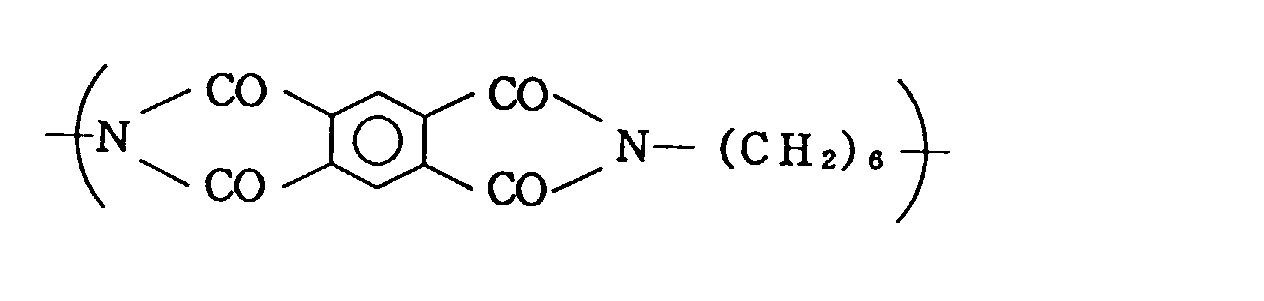

- In the present invention, it is possible to form a 20 - 300 nm thick insulating film, for short-circuit prevention, of Ta2O5, SiO2 or TiO2 between the
alignment control layer 7a (7b) and theprincipal electrodes 5a (5b). - The liquid crystal composition (the
composition 2 shown in Figure 1) used in the present invention may desirably contain a fluorine-containing mesomorphic compound which preferably has a structure including a fluorocarbon terminal portion and a hydrocarbon terminal portion connected by a central core and has smectic phase or latent smectic phase. The term "latent smectic phase" refers to a property of a compound concerned that the compound alone does not exhibit smectic phase but can be a component compatibly contained in smectic phase of a liquid crystal composition. - In a preferred class of the fluorine-containing mesomorphic compound, the fluorocarbon terminal portion may preferably be:
- a group represented by the formula -D1-CxaF2xa-X, where xa is 1 - 20; X is -H or -F; -D1- is -CO-O-(CH2)ra-, -O-(CH2)ra-, -(CH2)ra-, -O- SO2-, -SO2-, -SO2-(CH2)ra-, -O-(CH2)ra-O-(CH2)rb-, -(CH2)ra-N(CpaH2pa+1)-SO2- or -(CH2)ra-N(CpaH2pa+1)- CO-; where ra and rb are independently 1 - 20; and pa is 0 - 4; or
- a group represented by -D2-(CxbF2xb-O)za- CyaF2ya+1, wherein xb is 1 - 10 independently for each (CxbF2xb-O); ya is 1 - 10; za is 1 - 10; -D2- is -CO-O-CrcH2rc, -O-CrcH2rc- -CrcH2rc-, -O-(CsaH2sa- O)ta-CrdH2rd- -O-SO2-, -SO2-, -SO2-CrcH2rc-,-CrcH2rc-N(CpbH2pb+1)-SO2- -CrcH2rc-N(CpbH2pb+1)-CO-, or a covalent bond, where rc and rd are independently 1 - 20; sa is independently 1- 10 for each (CsaH2sa-O); ta is 1 - 6; and pb is 0 - 4.
- In the fluorine-containing mesomorphic used in the present invention, the mesomorphic compound may preferably have a central core comprising at least two rings independently selected from aromatic ring, heteroaromatic ring, cycloaliphatic ring, or substituted aromatic ring, substituted heteroaromatic ring, and substituted cycloaliphatic ring, which may be connected one with another by a covalent bond or by groups selected from -COO-, -COS-, -HC=N-, -COSe-. Rings may be fused or non-fused. Heteroatoms within the heteroaromatic ring comprise at least one atom selected from N, O or S. Non-adjacent methylene groups in cycloaliphatic rings may be substituted by O atom. The central core may preferably comprise a benzene ring and a pyrimidine ring.
- It is particularly preferred to use a fluorine-containing mesomorphic compound of the following general formula (I) or (II):

- wherein A1, A2 and A3 are each independently


- ga, ha and ia are independently an integer of 0 - 3 with the proviso that the sum of ga+ha+ia be at least 2;
- L1 and L2 are each independently a covalent bond, -CO-O-, -O-CO-, -COS-, -S-CO-, -CO-Se-, -Se-CO-, -CO-Te-, -Te-CO-, -CH2CH2-, -CH=CH-, -C≡C-, -CH=N-, -N=CH-, -CH2-O-, -O-CH2-, -CO- or -O-;
- X1, Y1 and Z1 are each a substituent of A1, A2 and A3, respectively, and each X1, Y1 and Z1 are independently -H, -Cl, -F, -Br, -I, -OH, -OCH3, -CH3, -CN or -NO2;
- each ja, ma and na are independently an integer of 0 - 4;
- J1 is -CO-O-(CHz)ra-, -O-(CH2)ra-, -(CH2)ra-, -O-SO2-, -SO2-, -SO2-(CH2)ra-, -O-(CH2)ra-O-(CH2)rb-, -(CH2)ra-N(CpaH2pa+1)-SO2- or -(CH2)ra-N(CpaH2pa+1)- CO-; where ra and rb are independently 1 - 20, and pa is 0 - 4;
- R1 is -O-CqaH2qa-O-CqbH2qb+1, -CqaH2qa-O- CqbH2qb+1, -CqaH2qa-R3, -O-CqaH21qa-R3, -CO-O-CqaH2qa- R3, or -O-CO-CqaH2qa-R3 which may be either straight chain or branched; where R3 is -O-CO-CqbH2qb+1, -CO-O- CqbH2qb+1, -H, -Cl, -F, -CF3, -NO2 or -CN; and qa and qb are independently 1 - 20;
- R2 is CxaF2xa-X, where X is -H or -F, xa is an integer of 1 - 20.

- wherein A4, A5 and A6 are each independently


- gb, hb and ib are each independently an integer of 0 - 3 with the proviso that the sum of gb+hb+ib be at least 2;
- each L3 and L4 are independently a covalent bond, -CO-O-, -O-CO-, -CO-S-, -S-CO-, -CO-Se-, -Se-CO-, -CO-Te-, -Te-CO-, -(CH2CH2)ka- (ka is 1 - 4), -CH=CH-, -C≡C-, -CH=N-, -N=CH-, -CH2-O-, -O-CH2-, -CO- or -O-;
- X2, Y2 and Z2 are each a substituent of A4, A5 and A6, respectively, and each X2, Y2 and Z2 are independently -H, -Cl, -F, -Br, -I, -OH, -OCH3, -CH3, -CF3, -O-CF3, -CN or -NO2; each jb, mb and nb are independently an integer of 0 - 4;
- J2 is -CO-O-CrcH2rc-, -O-CrcH2rc-, -CrcH2rc-, -O-(CsaH2sa-O)ta-CrdH2rd-, -O-SO2-, -SO2-, -SO2- CrcH2rc-, -CrcH2rc-N(CpbH2pb+1)-SO2- or -CrcH2rc- N(CpbH2pb+1)-CO-; rc and rd are independently 1 - 20; sa is independently 1 - 10 for each (CsaH2sa-O), ta is 1 - 6; pb is 0 - 4;
- R4 is -O-(CqcH2qc-O)wa-CqdH2qd+1, -(CqcH2qc-O)wa-CqdH2qd+1, -CqcH2qc-R6, -O-CqcH2qc-R6, -CO-O- CqcH2qc-R6, or O-CO-CqcH2qc-R6 which may be either straight chain or branched; R6 is -O-CO-CqdH2qd+1; -CO-O-CqdH2qd+1, -Cl, -F, -CF3, -NO2, -CN or -H; qc and qd are independently an integer of 1 - 20; wa is an integer of 1 - 10;
- R5 is (CxbF2xb-O)za-CyaF2ya+1, wherein xb is independently 1 - 10 for each (CxbF2xb-O); ya is 1 - 10; and za is 1 - 10.
- The fluorine-containing mesomorphic compound represented by the formula (I) may be synthesized through processes similar to those descried in JP-A (Kokai) 2-142753 and U.S. Patent No. 5,082,587. Specific examples of such a mesomorphic compound of the formula (I) may include those (Example Compound Nos. I-1 to I-103) shown below.


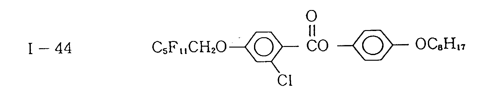


- The fluorine-containing mesomorphic compound represented by the formula (II) may be synthesized through processes similar to those descried in JP-A (Kohyo) 7-506368 and WO93/22396. Specific examples of such a mesomorphic compound of the formula (II) may include those (Example Compound Nos. II-1 to II-45) shown below.


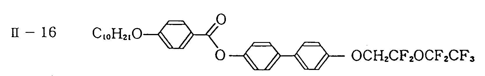


- In addition to at least one species of the above-mentioned mesomorphic compound of the formula (I), the liquid crystal composition according to the present invention may preferably contain at least one species of an optically active compound having an asymmetrical carbon atom (as a chiral dopant), thus being formulated as a chiral smectic liquid crystal composition.
- Particularly, when such a chiral smectic liquid crystal composition shows a larger spontaneous polarization of at least 10 nC/cm2, the resultant liquid crystal device (or apparatus) may suitably be used since the device provides more advantageous effects as described hereinbelow.
- The liquid crystal composition used in the present invention may further contain other compounds and additives, such as another mesomorphic compound, an antioxidant, an ultraviolet ray-absorbing agent, a dye and a pigment, as desired.
- Hereinbelow, an embodiment of a process for producing the liquid crystal device according to the present invention as shown in Figure 1 will be described with reference to Figures 2A - 2E and Figures 3A - 3F.
- Figures 2A - 2E shows a series of steps generally involved in a process for producing the (upper) electrode plate including the light-transmissive substrate la shown in Figure 1, and Figures 3A - 3F shows a series of steps generally involved in a process for producing the (lower) electrode plate including the light-
transmissive substrate 1b. - Referring to Figure 2A, a plurality of metal electrodes (as auxiliary electrodes) 3a are formed on a light-transmissive substrate (e.g., glass substrate) 1a by forming a metal layer thereon, followed by patterning of the metal layer.
- More specifically, the metal layer can be formed by a known film-forming process, such as vacuum vapor deposition, electron beam deposition, ion plating, chemical vapor deposition (CVD) or sputtering, depending on the metal species used. Further, the patterning of the metal layer can also be performed by, e.g., etching or photolithographic process, depending on the metal species used and/or a production process adopted.
- The surface (wiring surface) of the substrate la on which the
metal electrodes 3a are disposed may preferably be treated with, e.g., a silane coupling agent so as to enhance an adhesiveness with an insulatinglayer 4a formed in a later step. - On the (wiring) surface of the
substrate 1a, a predetermined amount of a polymeric material (uncured) 10 was placed by using a constant volume-supplying device (not shown), such as a dispenser, a roller coater or a spinner coater (Figure 2B). - Thereafter, on the surface of the substrate la provided with the
metal electrodes 3a and thepolymeric material 10, a smooth or smoothing mold substrate (hereinafter called "smooth plate") 9 is gradually superposed so as not to generate air bubbles therebetween, thus filling thepolymeric material 10 constituting an insulatinglayer 4a at spacings between themetal electrodes 3a (Figure 2C) (hereinafter, the structure as shown in Figure 2C is referred to as a "laminated structure"). - Then, the laminated structure is set within a press (not shown) and pressed thereby, thus removing an excessive polymeric material from the surface of the
metal electrodes 3a, whereby the spacings between themetal electrodes 3a are completely filled with thepolymeric material 10. - The
smooth plate 9 used in the above step may comprise any material if the resultant plate has a smooth surface and a property of being not deformed by pressure and optionally has a light-transmissive property in the case of using, e.g., UV light for curing thepolymeric material 10. In the present invention, a surface-polished glass plate may preferably be used as thesmooth plate 9. The press may be any one if it can uniformly extend thepolymeric material 10 so as to fill the spacings between themetal electrodes 3a. Examples of such a press may include one using a hydraulic or air cylinder, a liquid pressure press and a roller press. In the step of pressing the laminated structure, it is also possible to heat the laminated structure by using, e.g., an electric heater or heated fluid, whereby the viscosity of thepolymeric material 10 is effectively decreased to enhance a smooth extension thereof under pressure application. - When a UV-curable resin is used as the
polymeric material 10, the UV-curable resin can be cured by using a light source providing an output (energy) sufficient to completely cure the UV-curable resin. Examples of the light source may include a high- (or low-)pressure mercury-vapor lamp and a xenon lamp. - Then, the
smooth plate 9 is removed from the laminated structure by using a peeling device (not shown) (Figure 2D). - Thereafter, a plurality of
transparent electrodes 5a (as principal electrodes) are formed on themetal electrodes 3a and the insulating layer 4 in a similar manner as in themetal electrodes 3a so as to being electrically connected with the associatedmetal electrodes 3a, respectively, at at least a part of eachtransparent electrode 5a (Figure 2E). - On the other hand, the lower electrode plate including the light-transmissive substrate (e.g., glass substrate) 1b as shown in Figure 1 is prepared through the steps shown in Figures 3A - 3F in the same manner as in the above-described upper electrode plate (Figures 2A - 2E) except that a masking (light-interrupting)
member 6 is first formed on the light-transmissive substrate 1b as shown in Figure 3A. - The masking
member 6 can also be formed in the same manner as in themetal electrodes 3a described above so that the maskingmember 6 has at least a portion corresponding to each spacing between adjacenttransparent electrodes 5b formed in a later step as shown in Figure 3F. - Each of the thus-prepared (upper and lower) electrode plates is coated with an
alignment control layer 7a (or 7b), after being coated with an insulating film as desired, by a known coating method, such as a spin coating, a roller coating or printing. - On one or both of the thus-treated electrode plates,
spacer beads 8 as shown in Figure 1 are dispersed, and the electrodes plates are applied to each other with a prescribed spacing defined by thespacer beads 8 and a sealing member (not shown) disposed at the periphery of the electrode plates. Thereafter, the spacing between the electrode plates is filled with the above-mentioned liquid crystal composition (thecomposition 2 as shown in Figure 1), thus preparing a liquid crystal composition according to the present invention. - In the above embodiment, the
principal electrodes - The above-prepared liquid crystal device is disposed between a pair of polarizers (not shown) arranged in cross nicols.
- In the case where the liquid crystal device of the present invention is used as a display device, a backlight device (not shown) is disposed behind the light-
transmissive substrate 1a so that the maskingmember 6 is located closer to the viewer side. - The liquid crystal device according to the present invention is used as a display element (medium), for various liquid crystal apparatus, one embodiment of which is described below.
- Based on an arrangement appearing hereinbelow and data format comprising image data accompanied with scanning line address data and by adopting communication synchronization using a SYNC signal as shown in Figures 4 and 5, there is provided a liquid crystal display apparatus of the present invention which uses the liquid crystal device according to the present invention as a display panel portion.
- Referring to Figure 4, a (chiral smectic) liquid
crystal display apparatus 101 includes agraphic controller 102, adisplay panel 103, a scanningline drive circuit 104, a dataline drive circuit 105, adecoder 106, ascanning signal generator 107, ashift resistor 108, a line memory 109, adata signal generator 110, a drive control circuit 111, a graphic central processing unit (GCPU) 112, a host central processing unit (host CPU) 113, and an image data storage memory (video-RAM or VRAM) 114. - Image data are generated in the
graphic controller 102 in an apparatus body and transferred to adisplay panel 103 by signal transfer means. Thegraphic controller 102 principally comprises theGCPU 112 and theVRAM 114 and is in charge of management and communication of image data between thehost CPU 113 and the liquidcrystal display apparatus 101. A light source (not shown) is disposed at the back of thedisplay panel 103. - The liquid crystal display apparatus of the present invention employs the above-described liquid crystal device showing a good switching characteristic as a display panel (medium), so that the display apparatus exhibits excellent drive characteristics and reliability and provides high-definition and large-area display images at high speed.
- The liquid crystal device according to the present invention may be driven by driving methods as disclosed in, e.g., JP-A 59-193426, JP-A 59-193427, JP-A 60-156046 and JP-A 60-156047.
- Figures 8A and 8B are waveform diagrams showing an example set of driving waveforms used in such a driving method. Figure 7 is a plan view showing an electrode matrix used in a (chiral smectic) liquid crystal panel (device) 131 of a simple matrix-type. The
liquid crystal panel 131 shown in Figure 7. includes scanning electrodes 132 (S1, S2, S3, ... Sm) and data electrodes 133 (I1, I2, I3, ... In) intersecting each other so as to constitute a pixel at each intersection together with a (chiral smectic) liquid crystal disposed between the scanningelectrodes 132 anddata electrodes 133. - Referring to Figure 8A, at SS is shown a selection scanning signal waveform applied to a selected scanning line, at SN is shown a non-selection scanning signal waveform applied to a non-selected scanning line, at IS is shown a selection data signal waveform (providing a black (dark) display state) applied to a selected data line, and at IN is shown a non-selection data signal waveform (providing a white (bright) display state) applied to a non-selected data line. Further, at IS - SS and IN - SS in the figure are shown voltage waveforms applied to pixels on a selected scanning line, whereby a pixel supplied with the voltage IS - SS assumes a black display state and a pixel supplied with the voltage IN - SS assumes a white display state. Figure 8B shows a time-serial waveform used for providing a display state as shown in Figure 6.
- In the driving embodiment shown in Figures 8A and 8B, a minimum duration (application time) Δt of a single polarity voltage applied to a pixel on a selected scanning line corresponds to the period of a writing phase t2, and the period of a one-line clearing phase t1 is set to 2Δt.
- The parameters VS, VI and Δt in the driving waveforms shown in Figures 8A and 8B are determined depending on switching characteristics of a liquid crystal material used.
- Figure 9 shows a V - T characteristic, i.e., a change in transmittance T when a driving voltage denoted by (VS+VI) is changed while a bias ratio (as mentioned hereinbelow) is kept constant. In this embodiment, the parameters are fixed at constant values of Δt = 50 µs and a bias ratio VI/(VI+VS) = 1/3. On the right side of Figure 9 is shown a result when the voltage (IN-SS) shown in Figure 8A is applied to a pixel concerned, and on the left side of Figure 9 is shown a result when the voltage (IS-SS) is applied to a pixel concerned, respectively while increasing the voltage (VS+VI)· On both sides of the ordinate, the absolute value of the voltage (VS+VI) is separately indicated. At (IN-SS) and (IS-SS), a previous (display) state is cleared by applying a voltage VR and a subsequent (display) state is determined by voltages VB 1 and VB 2, respectively. Referring to Figure 9, a relationship of V2 < V1 < V3 holds. The voltage V1 may be referred to as a threshold voltage in actual drive and the voltage V3 may be referred to as a crosstalk voltage. More specifically, as shown in Figure 8A, a voltage V1 denotes a voltage value causing switching by applying a voltage signal VB 2 and a voltage V3 denotes a voltage value causing switching by applying a voltage signal VB 1. Further, a voltage V2 denotes a voltage value required for clearing the previous state by applying a voltage signal VR. The crosstalk voltage V3 generally exists in actual matrix drive of a (chiral smectic) liquid crystal device. In an actual drive, M2(V) = (V3-V1)/(V3+V1) can be used as a factor of a voltage range of |VS+VI| allowing a matrix drive and may be referred to as a voltage margin parameter, which is preferably large enough. It is of course possible to increase the value of V3 by increasing the bias ratio (i.e., by causing the bias ratio to approach a unity). However, a large bias ratio corresponds to a large amplitude of a data signal and leads to an increase in flickering and a lower contrast, thus being undesirable in respect of image quality. According to our study, a bias ratio of about 1/3 - 1/4 was practical. On the other hand, when the bias ratio is fixed, the voltage margin parameter M2(V) largely depends on the switching characteristics of a liquid crystal material used and the device structure, and it is needless to say that a liquid crystal material providing a large M2(V) is very advantageous for matrix drive.
- Further, it is possible to drive the liquid crystal device by changing a voltage application time (duration) Δt while keeping the driving voltage (VI+VS) so as to provide a certain (constant) value. In this case, the drive characteristic of the liquid crystal device can also be evaluated in terms of a duration margin parameter (voltage application time margin parameter) M2(ΔT) = (Δt2-Δt1)/(Δt2+Δt1) wherein Δt1 denotes a threshold duration and Δt2 denotes a crosstalk duration.
- As described above, by appropriately changing the directions (signs) of two different data signals, it is possible to control display state so that selected pixels are appropriately written in two states of "black" and "white" and non-selected pixels can retain the written "black" and "white" states at a certain temperature. The above-described voltage and duration margin parameters M2(V) and M2(Δt) vary depending on and are intrinsic to a liquid crystal material used and a cell structure employed. Further, the M2(V) and M2(Δt) also fluctuate according to a change in environmental temperature, so that optimum driving conditions should be required for an actual display apparatus in view of a liquid crystal material used, a cell (device) structure and an environmental temperature.
- Next, another embodiment of the liquid crystal device of the present invention with reference to Figure 10 in combination with Figure 1.
- In this embodiment, a liquid crystal device has a cell structure identical to that described in the above-described embodiment (based on Figures 1 - 3) except that the lower electrode plate including the
substrate 1b (shown in Figure 1 and Figures 3A - 3F) is charged to an electrode plate shown in Figure 10 including a color filter, thus constituting a color liquid crystal (display) device. - Referring to Figure 10, the (lower) electrode plate includes: a light-
transmissive substrate 1; a maskingmember 6 disposed on thesubstrate 1, a color filter comprisingcolor filter segments 21R, 21G and 21B of red (R), green (G) and blue (B), disposed on thesubstrate 1 and separated from each other by the maskingmember 6; a flattening (or protective)layer 22 disposed so as to cover thecolor filter segments 21R, 21G and 21B; a plurality ofauxiliary electrodes 3 disposed with spacing therebetween on theflattening layer 22; a plurality ofprincipal electrodes 5 disposed on theflattening layer 22 so as to substantially fill the spacings between the auxiliary electrodes 3 (but leave a gap between each principal electrode and adjacent auxiliary electrode) while contacting and covering the top surface of the associatedauxiliary electrodes 3; and an alignment control layer 7 disposed so as to cover theprincipal electrode 5. - The above electrode plate (including the color filter) may preferably be disposed at a viewer (light-outputting) side in view of prevention of color mixing and include a plurality of data electrodes (comprising the principal and
auxiliary electrodes 5 and 3) to which a data signal is applied. On the other hand, the upper electrode plate including the substrate la (shown in Figure 1) includes a plurality of scanning electrodes (comprising the principal andauxiliary electrodes - In this embodiment, the color filter (21R, 21G, 21B) is located closer to the viewer side as mentioned above. This is because it is possible to adopt a conventional step for forming a color filter to allow a lot of latitude in cell structure design and it is also possible to provide a larger opening (light-transmission) region by disposing the color filter on the substrate provided with the data electrodes in the liquid crystal device of a simple matrix-type. In the case where the liquid crystal device is not used for displaying color images, it is possible to omit the
color filter segments 21R, 21G and 21B and theflattening layer 22. - In this embodiment, the
auxiliary electrodes 3 may be disposed on theprincipal electrodes 5 or may be omitted, as desired. - The
auxiliary electrodes 3 may preferably be made thin, e.g., in a thickness of at most 0.3 µm, so as not to provide the alignment control layer 7 with a larger unevenness which adversely affects an alignment state of liquid crystal molecules. - Further, in the case where only one of the
alignment control layers 7 and 7a is subjected to a uniaxial aligning (e.g., rubbing) treatment, the uniaxial aligning treatment may preferably be performed to thealignment control layer 7a of the upper electrode plate as shown in Figure 1. This is because the alignment of liquid crystal molecules is largely affected by the alignment control layer which has been subjected to the uniaxial aligning treatment, so that the surface of the alignment control layer may preferably be well flattened. - The uniaxial aligning treatment may preferably be performed in a direction nonparallel with a longitudinal direction of the electrodes in view of prevention of an occurrence of alignment defects. In a preferred embodiment, the direction of the uniaxial aligning treatment may preferably form an angle of at most 30 degrees with respect to the longitudinal direction of the electrode and may particularly desirably be aligned with the longitudinal direction of the electrodes.
- The masking
member 6,principal electrodes 5,auxiliary electrodes 3 and alignment control layer 7 shown in Figure 10 may comprise materials identical to those described above, respectively. - The color filter (
segments 21R, 21G and 21B) may be any color filter of, e.g., a pigment-dispersion type or a dye-type, and may be formed by various methods, such as a photolithography, a wet-coating (or printing) method, an ink jet method, and a sublimation method, depending on the material used. - The
flattening layer 22 may comprise an organic material or an inorganic material, as desired. Theflattening layer 22 may preferably be formed by wet coating so as not to damage the color filter. - As described above, in this embodiment, one electrode plate including the
substrate 1a provided with the scanning electrodes as shown in Figure 1 and the other electrode plate including thesubstrate 1 provided with the data electrodes as shown in Figure 10 are used in combination to provide a liquid crystal device according to the present invention. - In preparation of the electrode plate shown in Figure 10, the formation of the insulating layer disposed between the auxiliary electrode is unnecessary, thus reducing the production cost.
- According to our simulation, it has been formed that the scanning electrodes having a larger resistivity (electric resistance) cause a larger voltage waveform distortion but the data electrodes having a larger resistivity do not cause so larger voltage waveform distortion. More specifically, when the resistivity of the data electrodes is 40 times that of the scanning electrodes, the data and scanning electrodes have a substantially identical influence on the voltage waveform distortion.
- From the results of such a simulation, we assume that the voltage waveform distortion is attributable to an inversion current passing through the electrodes when a voltage in excess of a threshold voltage is applied to the liquid crystal layer. It is also assumed that the magnitude of such an inversion current is directly proportional to that of a spontaneous polarization of the liquid crystal composition used. Accordingly, as the liquid crystal composition has a larger spontaneous polarization, the voltage waveform distortion becomes larger, thus requiring a lowered resistivity of the electrodes employed.
- The inversion current presumably generated at the time of applying a voltage larger than a threshold voltage to the liquid crystal composition. When a selected pixel is supplied with such a voltage (over the threshold voltage), the voltage is generally applied to all the pixels in alignment with the selected pixel on the identical scanning line (electrode). At this time, pixels other than the selected pixel on the identical data line (electrode) are generally not supplied with the above voltage. In other words, all the portions of the liquid crystal composition with respect to the pixels on the scanning line contribute to the generation of the inversion current but only a portion of the liquid crystal composition with respect to the selected pixel on the data line contributes to the generation of the inversion current.
- From the above consideration, the distortion (or delay) of voltage waveform is presumed to be largely affected by a charge in resistivity of the scanning electrodes.
- Hereinbelow, the present invention will be described more specifically based on Examples. It is however to be understood that the present invention is not restricted to these Examples.
- A liquid crystal display device including a pair of electrode plates was prepared in the following manner.
- A 80 nm-thick masking member of Cr was formed on a double side-polished blue plate glass (300x310x1.1 mm) by sputtering, followed by patterning through a photolithographic process including an etching step to form a glass substrate provided with the masking member including elongated portions in a width of 30 µm at a pitch of 320 µm as shown in Figure 3A.
- On the glass substrate having thereon the masking member, a 2 µm-thick layer of Al was formed by sputtering and patterned in a width of 18 µm at a pitch of 320 µm by a photolithographic process including an etching step to form a plurality of auxiliary electrodes as shown in Figure 3B.
- On the surface (where the auxiliary electrodes are formed) of the glass substrate, a coupling treatment liquid comprising 1 wt. part of a silane coupling agent ("A-174", mfd. by Nippon Unicar K.K.) and 40 wt. parts of ethyl alcohol was applied by spin coating, followed by heat-treatment in an oven at 100 °C for 20 min.
- On the thus-treated surface of the glass substrate, an acrylic UV-curable resin comprising a mixture of pentaerythritol triacrylate/neopentyl glycol diacrylate/1-hydroxycyclohexyl phenyl ketone (= 50/50/2 by weight) was placed dropwise by using a dispenser as shown in Figure 3C.
- Further thereon, a smooth plate (double side-polished blue plate glass; 300x310 mm) was gradually superposed so as not to generate air bubbles therebetween. Thereafter, the glass substrate and the smooth plate were pressed in a 1 ton roller press under a pressure of 700 kg at a feed rate of 30 cm/min. The laminate of the glass substrate and the smooth plate, after taking out from the roller press, was irradiated with UV rays for 2 min. by using a UV ray irradiation apparatus including four 100 W-high pressure mercury vapor lamps to curve the UV-curable resin (Figure 3D).
- Then, the smooth plate was removed from the glass substrate by using a releasing tool (Figure 3E).
- On the auxiliary electrodes and the UV-cured resin formed on the glass substrate, a 150 nm-thick ITO film was formed by sputtering, followed by patterning of the ITO film so as to be electrically connected to associated auxiliary electrodes through a photolithographic-etching process to form a plurality of principal (transparent) electrodes each having a width of 300 µm and a pitch of 320 µm.
- The thus prepared electrode plate was provided with the masking member arranged so as to interrupt light passing through spacings between the principal electrodes.
- The other electrode plate was prepared in the same manner as in the first electrode plate except that the masking member was not formed as shown in Figures 2A - 2E.
- Then, the electrode plate (including the masking member) was coated with a mixture of a ladder-type polysiloxane containing SnOx fine particles (particle size = 100 Å) dispersed therein and ethanol (solid content = 10 wt. %) by spin coating, followed by pre-drying at 80 °c for 5 min. and hot baking at 200 °C for 1 hour to form a 2000 Å-thick layer.
- The other electrode plate (including no masking member) was coated with a 0.8 wt. %-solution of a polyimide precursor having a recurring unit represented by the formula shown below, followed by pre-drying at 80 °C for 5 min. and hot baking at 200 °C for 1 hour to form a 6 nm-thick alignment control layer, which was then subjected to rubbing treatment with a nylon cloth to effect a uniaxial aligning treatment.

- After silica beads (average particle size = 2 pm) were dispersed on one of the electrode plates, the electrode plates were applied to each other with a sealing member so that the electrodes of one electrode plate and those of the other electrode plate were arranged in a matrix form to form a blank cell, which was then filled with a liquid crystal composition A (Composition A) shown below in its isotropic liquid state, followed by cooling to room temperature at a rate of 1 °C/min. to prepare a liquid crystal device as shown in Figure 1.


- Then, a pair of polarizers were applied (bonded) to both sides of the liquid crystal device so as to provide a cross nicol relationship.
- Behind the liquid crystal device (on the side closer to the electrode plate including no masking member), a backlight device was disposed, thus preparing a liquid crystal display device to be viewed from the side of the electrode plate including the masking member.
- The thus prepared liquid crystal display device provided a uniform alignment of the liquid crystal composition A due to a reduced unevenness at the boundaries between the electrode plates and the liquid crystal composition A and showed a decreased voltage waveform distortion. Further, the device could effect uniform switching when driven and also could effect display without malfunction even at the time of high-speed switching. In addition, a portion corresponding to the spacing between the principal electrodes was covered with the masking member to completely prevent leakage of light from a non-switching region, thus allowing a high quality display providing a contrast of at least 100.
- A liquid crystal display device was prepared in the same manner as in Example 1 except that the liquid crystal composition A was changed to a liquid crystal composition B shown below.


- In the above phase transition series, Sx denotes a smectic phase (unidentified); Sc denotes a smectic C phase; SA denotes a smectic A phase; and Iso denotes an isotropic phase.
- The liquid crystal display device, similarly as in Example 1, provided a uniform alignment and could effect high quality display without malfunction at the time of high-speed switching. Further, the device provided a contrast of at least 100.
- A liquid crystal display device was prepared in the following manner.
- One electrical plate was prepared in the same manner as in the electrode plate including no masking member (as shown in Figures 2A - 2E) in Example 1.
- The other electrode plate as shown in Figure 10 was prepared as follows.
- On a double side-polished blue plate glass (300x310x1.1 mm), a 20 µm-thick layer of Mo-Ta was formed by sputtering and patterned through a photolithographic-etching to form a glass substrate coated with a masking member including elongated portions each having a width of 18 µm.
- On the glass substrate, a photosensitive resin solution containing a green pigment dispersed therein was applied by spin coating and pre-dried at 80 °C, followed by spin coating and pre-dried at 80 °C, followed by exposure to light, development and hot backing at 250 °C to form 1.3 µm-thick stripe-shaped color filter segments of green in a width of 95 µm. Similarly, a photosensitive resin solution containing a red pigment and a photosensitive resin solution containing blue pigment were successively used for forming red color filter segments and blue color filter segments, respectively. The resultant color filter included color filter segments of green, red and blue each having a width of 95 µm at a spacing therebetween of 8 µm.
- In this step, the photosensitive resin solution for green comprised a 10 %-solution of a photosensitive resin in N-methyl-2-pyrrolidone ("PA-1000", mfd. by Ube Kosan K.K.) and a green pigment ("Lionol Green GYK" (C.I. No. 74265), mfd. by Toyo Inki Seizo K.K.) dispersed therein in a ratio of pigment:resin = 1:2. The photosensitive resin solution for red comprised a 10 %-solution of a photosensitive resin in N-methyl-2-pyrrolidone ("PA-1000", mfd. by Ube Kosan K.K.) and a red pigment ("Irgagin Red BRT" (C.I. No. 71127), mfd. by Ciba-Geigy Corp.) dispersed therein in a ratio of pigment:resin = 1:2. The photosensitive resin solution for blue comprised a 10 %-solution of a photosensitive resin in N-methyl-2-pyrrolidone ("PA-1000", mfd. by Ube Kosan K.K.) and a blue pigment ("Heliogen Blue L7080" (C.I. No. 74160), mfd. by BASF Co.) dispersed therein in a ratio of pigment:resin = 1:2.
- On the color filter, a 3 µm-thick flattening layer was formed by applying and baking an acrylic resin ("LC-2040", mfd. by Sanyo Kasei Kogyo K.K.).
- Thereafter, on the flattening layer, 8 µm-wide auxiliary electrodes including three layers of Ta-Mo (30 nm)/Al-Si-Cu (150 nm)/Ta-Mo (50 nm) were formed by sputtering and patterning.
- On the auxiliary electrodes and the flattening layer, 70 nm-thick principal (transparent) electrodes of ITO were formed by sputtering and patterned by a photolithographic-etching process in a stripe shape including alternating 47 µm-wide elongated electrodes and 30 µm-wide elongated electrodes each with a spacing of 8 pm.
- Then, on the principal electrodes, a mixture of a ladder-type polysiloxane containing SnOx fine particles (particle size = 100 Å) dispersed therein and ethanol (solid content = 10 wt. %) was applied by spin coating, followed by pre-drying at 80 °C for 5 min. and hot baking at 200 °C for 1 hour to form a 2000 Å-thick alignment control layer, thus preparing an electrode plate.
- The thus-prepared pair of electrode plates were used for preparing a liquid crystal display device in the same manner as in Example 1.
- The resultant liquid crystal display device provided similar effects as in Example 1.
- As described hereinabove, according to the present invention, it is possible to realize a liquid crystal device providing an excellent alignment state of liquid crystal molecule while minimizing the voltage waveform distortion based on a specific combination of a liquid crystal composition containing the fluorine-containing mesomorphic compound of the formula (I) stably providing a bookshelf structure or a layer structure close thereto and an electrode plate including auxiliary electrodes embedded with an insulating resin. The resultant liquid crystal device is also excellent in contrast, resolution and brightness and is capable of effecting a good motion-picture display in a large picture area.
- When the liquid crystal device was used in combination with, e.g., a driving means and a backlight device, it is possible to provide a liquid crystal (display) apparatus excellent in display characteristics.
Claims (40)
- A liquid crystal device, comprising: a pair of electrode plates and a liquid crystal composition disposed between the electrode plates,wherein at least one of the electrode plates comprises a light-transmissive substrate, a plurality of electrodes including principal electrodes and auxiliary electrodes supported on the light-transmissive substrate, and an insulating layer; each auxiliary electrode being disposed between an associated principal electrode and the light-transmissive substrate so as to be electrically connected with at least a part of the associated principal electrode, and the auxiliary electrodes being disposed with spacings therebetween which are filled with the insulating layer, andthe liquid crystal composition comprises at least one species of a fluorine-containing mesomorphic compound comprising a fluorocarbon terminal portion and a hydrocarbon terminal portion, the terminal portions being connected with a central core, and having smectic mesophase or latent smectic mesophase.
- A device according to Claim 1, wherein the insulating layer comprises a polymeric material.
- A device according to Claim 2, wherein the polymeric material comprises a ultraviolet-cured resin.
- A device according to any preceding claim, wherein each of the electrode plates is provided with an alignment control layer.
- A device according to Claim 4, wherein the alignment control layer provided to one electrode plate is subjected to a uniaxial aligning treatment and the alignment control layer provided to the other electrode plate is not subjected to a uniaxial aligning treatment.
- A device according to Claim 5, wherein the alignment control layer to be subjected to the uniaxial aligning treatment comprises a polyimide film.
- A device according to any preceding claim, wherein the surface of the auxiliary electrodes and the surface of the light-transmissive substrate provided a distance therebetween larger than a distance between the surface of the insulating layer and the light-transmissive substrate.
- A device according to any preceding claim, wherein the principal electrodes comprises transparent electrodes.
- A device according to any preceding claims, wherein at least one of the electrode plates further comprises a masking member including a plurality of masking portions disposed on the light-transmissive substrate, each masking portion being disposed so as to correspond to a spacing between associated adjacent principal electrodes.
- A device according to Claim 9, wherein the masking member is electroconductive and each masking portion is electrically connected with an associated auxiliary electrode.
- A device according to any preceding claim, wherein said fluorocarbon terminal portion in the fluorine-containing mesomorphic compound is represented by the formula -D1-CxaF2xa-X, where xa is 1 - 20; X is -H or -F; -D1- is -CO-O-(CH2)ra-, -O-(CH2)ra-, -(CH2)ra-, -O-SO2-, -SO2-, -SO2-(CH2)ra-, -O-(CH2)ra-O-(CH2)rb-, -(CH2)ra-N(CpaH2pa+1)-SO2- or -(CH2)ra-N(CpaH2pa+1)- CO- where ra and rb are independently 1 - 20; and pa is 0 - 4.
- A device according to any of Claims 1-10, wherein said fluorocarbon terminal portion in the fluorine-containing mesomorphic compound is represented by the formula -D2-(CxbF2xb-O)za-CyaF2ya+1, where xb is independently 1 - 10 for each (CxbF2xb-O); ya is 1 - 10; za is 1 - 10; -D2- is -CO-O-CrcH2rc, -O-CrcH2rc-, -CrcH2rc-, -O-(CsaH2sa-O)ta-CrdH2rd-, -O-SO2-, -SO2-, -SO2-CrcH2rc-, -CrcH2rc-N(CpbH2p+1)-SO2-, -CrcH2rc- N(CpbH2pb+1)-CO-, or a covalent bond where rc and rd are independently 1 - 20; sa is independently 1 - 10 for each (CsaH2sa-O); ta is 1 - 6; and pb is 0 - 4.
- A device according to any of Claims 1-10, wherein said fluorine-containing mesomorphic compound is represented by the following general formula (I):
 wherein A1, A2 and A3 are each independently
 ga, ha and ia are independently an integer of 0 - 3 with the proviso that the sum of ga+ha+ia be at least 2;L1 and L2 are independently a covalent bond, -CO-O-, -O-CO-, -COS-, -S-CO-, -CO-Se-, -Se-CO-, -CO-Te-, -Te-CO-, -CH2CH2-, -CH=CH-, -C≡C-, -CH=N-, -N=CH-, -CH2-O-, -O-CH2-, -CO- or -O-;X1, Y1 and Z1 are each a substituent of A1, A2 and A3, respectively, and each X1, Y1 and Z1 are independently -H, -Cl, -F, -Br, -I, -OH, -OCH3, -CH3, -CN or -NO2;each ja, ma and na are independently an integer of 0 - 4;J1 is -CO-O-(CH2)ra-, -O-(CH2)ra-, -(CH2)ra-, -O-SO2-, -SO2-, -SO2-(CH2)ra-, -O-(CH2)ra-O-(CH2)rb-, -(CH2)ra-N(CpaH2pa+1)-SO2- or -(CH2)ra-N(CpaH2pa+1)- CO- where ra and rb are independently 1 - 20, and pa is 0 - 4;R1 is -O-CqaH2qa-O-CqbH2qb+1, -CqaH2qa-O-CqbH2qb+1, -CqaH2qa-R3, -O-CqaH2qa-R3, -CO-O-CqaH2qa-R3, or -O-CO-CqaH2qa-R3 which may be either straight chain or branched where R3 is -O-CO-CqbH2qb+1, -CO-O-CqbH2qb+1, -H, -Cl, -F, -CF3, -NO2 or -CN; and qa and qb are independently 1 - 20; andR2 is CxaF2xa-X, wherein X is -H or -F, xa is an integer of 1 - 20.
 - A device according to any of claims 1-10, wherein said fluorine-containing mesomorphic compound is represented by the general formula (II):

 where A4, A5 and A6 are each independently denote
 gb, hb and ib are each independently an integer of 0 - 3 with the proviso that the sum of gb+hb+ib be at least 2;each L3 and L4 are independently a single bond, -CO-O-, -O-CO-, -CO-S-, -S-CO-, -CO-Se-, -Se-CO-, -CO-Te-, -Te-CO-, -(CH2CH2)ka- (ka is 1 - 4), -CH=CH-, -C≡C-, -CH=N-, -N=CH-, -CH2-O-, -O-CH2-, -CO- or -O-;X2, Y2 and Z2 are each a substituent of A4, A5 and A6, respectively, and each X2, Y2 and Z2 are independently -H, -Cl, -F, -Br, -I, -OH, -OCH3, -CH3, -CF3, -O-CF3, -CN or -NO2; each jb, mb and nb are independently an integer of 0 - 4;J2 is -CO-O-CrcH2rc-, -O-CrcH2rc-, -CrcH2rc-, -O-(CsaH2sa-O)ta-CrdH2rd-, -O-SO2-, -SO2-, -SO2- CrcH2rc-, -CrcH2rc-N(CpbH2pb+1)-SO2- or -CrcH2rc-N(CpbH2pb+1)-CO- where rc and rd are independently 1 - 20; sa is independently 1 - 10 for each (CsaH2sa-O), ta is 1 - 6; pb is 0 - 4;R4 is -O-(CqcH2qc-O)wa-CqdH2qd+1, -(CqcH2qc-O)wa-CqdH2qd+1, -CqcH2qc-R6, -O-CqcH2qc-R6, -CO-O- CqcH2qc-R6, or O-CO-CqcH2qc-R6 which may be either straight chain or branched where R6 is -O-CO-CqdH2qd+1; -CO-O-CqdH2qd+1, -Cl, -F, -CF3, -NO2, -CN or -H; qc and qd are independently 1 - 20; wa is 1 - 10; andR5 is (CxbF2xb-O)za-CyaF2ya+1, where xb is independently 1 - 10 for each (CxbF2xb-O); ya is 1 - 10; and za is 1 - 10.
 - A liquid crystal apparatus, including a liquid crystal device according to any one of Claims 1 - 14 and means for driving the liquid crystal device.
- A liquid crystal device, comprising: a pair of first and second electrode plates and a liquid crystal composition disposed between the electrode plates,wherein the first electrode plates comprises a light-transmissive substrate, a plurality of electrodes including principal electrodes and auxiliary electrodes supported on the light-transmissive substrate, and an insulating layer; each auxiliary electrode being disposed between an associated principal electrode and the light-transmissive substrate so as to be electrically connected with at least a part of the associated principal electrode, and the auxiliary electrodes being disposed with spacings therebetween which are filled with the insulating layer, andthe second electrode plate comprises a light-transmissive substrate and a plurality of electrodes including principal electrodes and auxiliary electrodes disposed on the light-transmissive substrate, each auxiliary electrode being disposed between an associated principal electrode and the light-transmissive substrate so as to be electrically connected with at least a part of the associated principal electrode, and each principal electrode contacting the light-transmissive substrate at a spacing between an associated auxiliary electrode and an adjacent auxiliary electrode.
- A device according to Claim 16, wherein each of the first and second electrode plates is provided with an alignment control layer, only the alignment control layer provided to the first electrode plate being subjected to a uniaxial aligning treatment.
- A device according to Claim 16 or 17, wherein the liquid crystal composition comprises at least one species of a fluorine-containing mesomorphic compound comprising a fluorocarbon terminal portion and a hydrocarbon terminal portion, the terminal portions being connected with a central core, and having smectic mesophase or latent smectic mesophase.
- A device according to Claim 16, 17 or 18, wherein the insulating layer comprises a polymeric material.
- A device according to Claim 17, wherein the alignment control layer to be subjected to a uniaxial aligning treatment comprises a polyimide film.
- A device according to any of Claims 16-20, wherein the principal electrodes comprises transparent electrodes.
- A device according to any of Claims 16-21, wherein the light-transmissive substrate of the first electrode plate or the second electrode plate is provided with a masking member.
- A liquid crystal apparatus including a liquid crystal device according to any of Claims 16-22 and means for driving the liquid crystal device.
- An apparatus according to Claim 23, wherein the plurality of electrodes of the first electrode plate are supplied with a scanning signal and those of the second electrode plate are supplied with a data signal.
- A liquid crystal device, comprising: a pair of first and second electrode plates and a liquid crystal composition disposed between the electrode plates,wherein the first electrode plates comprises a light-transmissive substrate, a plurality of electrodes including principal electrodes and auxiliary electrodes supported on the light-transmissive substrate, and an insulating layer; each auxiliary electrode being disposed between an associated principal electrode and the light-transmissive substrate so as to be electrically connected with at least a part of the associated principal electrode, and the auxiliary electrodes being disposed with spacings therebetween which are filled with the insulating layer, andthe second electrode plate comprises a light-transmissive substrate, a color filter disposed on the light-transmissive substrate, a flattening layer disposed on the color filter, and a plurality of electrodes including principal electrodes and auxiliary electrodes disposed on the flattening layer; each auxiliary electrode being disposed between an associated principal electrode and the flattening layer so as to be electrically connected with at least a part of the associated principal electrode, and each principal electrode contacting the flattening layer at a spacing between an associated auxiliary electrode and an adjacent auxiliary electrode.
- A device according to Claim 25, wherein each of the first and second electrode plates is provided with an alignment control layer, only the alignment control layer provided to the first electrode plate being subjected to a uniaxial aligning treatment.
- A device according to Claim 25 or 26, wherein the liquid crystal composition comprises at least one species of a fluorine-containing mesomorphic compound comprising a fluorocarbon terminal portion and a hydrocarbon terminal portion, the terminal portions being connected with a central core, and having smectic mesophase or latent smectic mesophase.
- A device according to Claim 25, 26 or 27, wherein the insulating layer comprises a polymeric material.
- A device according to Claim 26, wherein the alignment control layer to be subjected to a uniaxial aligning treatment comprises a polyimide film.
- A device according to any of Claims 25-29, wherein the principal electrodes comprises transparent electrodes.
- A device according to any of Claims 25-30, wherein the light-transmissive substrate of the first electrode plate or the second electrode plate is provided with a masking member.
- A liquid crystal apparatus including a liquid crystal device according to any of Claims 25-31, a backlight device disposed outside the first electrode plate and means for driving the liquid crystal device.
- An apparatus according to Claim 32, wherein the plurality of electrodes of the first electrode plate are supplied with a scanning signal and those of the second electrode plate are supplied with a data signal.
- An electrode plate for a liquid crystal device comprising a light transmissive substrate and electrodes on the substrate spaced apart at a pitch defining a pixel dimension, wherein each electrode comprises an auxiliary electrode of relatively low resistance material and which is smaller than the pixel and a principal electrode of relatively high resistance material and whose size corresponds to that of the pixel, the principal electrode being connected to the auxiliary electrode in a region where they overlap.
- The plate of Claim 34, wherein the auxiliary electrode comprises a metal or a resin having electroconductive fine particles dispersed therein.
- The plate of Claim 34 or 35, wherein the auxiliary electrodes are of thickness 0.3-3µm.
- The plate of any of Claims 34-36, wherein the principal electrodes comprise a transparent oxide.
- The plate of Claim 37, wherein the principal electrodes comprise indium oxide, tin oxide or indium tin oxide.
- A method for forming an electrode plate for a liquid crystal device which comprises:(a) forming on a light transmissive substrate auxiliary electrodes of relatively low resistance material, the auxiliary electrodes being spaced apart at a pitch defining a pixel dimension and the auxiliary electrodes being smaller than the pixel dimension;(b) coating the substrate with a UV-curable resin;(c) pressing a smooth plate against the coated substrate and curing the resin;(d) removing the smooth plate to give a flat surface at which the auxiliary electrodes appear, separated by cured resin; and(e) depositing principal electrodes of relatively higher resistance material whose size corresponds to that of the pixels, the principal electrodes being connected to the auxiliary electrodes in regions where they overlap.
- The method of Claim 39, comprising the further step of coating the plate with a layer of polymeric material.
Priority Applications (1)
| Application Number | Priority Date | Filing Date | Title |
|---|---|---|---|
| EP00204626A EP1088877A3 (en) | 1996-06-17 | 1997-06-16 | Liquid crystal device and liquid crystal apparatus |
Applications Claiming Priority (4)
| Application Number | Priority Date | Filing Date | Title |
|---|---|---|---|
| JP15550396 | 1996-06-17 | ||
| JP155503/96 | 1996-06-17 | ||
| JP9153664A JPH1068923A (en) | 1996-06-17 | 1997-06-11 | Liquid crystal element and liquid crystal device using that |
| JP153664/97 | 1997-06-11 |
Related Child Applications (1)
| Application Number | Title | Priority Date | Filing Date |
|---|---|---|---|
| EP00204626A Division EP1088877A3 (en) | 1996-06-17 | 1997-06-16 | Liquid crystal device and liquid crystal apparatus |
Publications (2)
| Publication Number | Publication Date |
|---|---|
| EP0814142A2 true EP0814142A2 (en) | 1997-12-29 |
| EP0814142A3 EP0814142A3 (en) | 1998-12-16 |
Family
ID=26482218
Family Applications (2)
| Application Number | Title | Priority Date | Filing Date |
|---|---|---|---|
| EP00204626A Withdrawn EP1088877A3 (en) | 1996-06-17 | 1997-06-16 | Liquid crystal device and liquid crystal apparatus |
| EP97304210A Withdrawn EP0814142A3 (en) | 1996-06-17 | 1997-06-16 | Liquid crystal device and liquid crystal apparatus |
Family Applications Before (1)
| Application Number | Title | Priority Date | Filing Date |
|---|---|---|---|
| EP00204626A Withdrawn EP1088877A3 (en) | 1996-06-17 | 1997-06-16 | Liquid crystal device and liquid crystal apparatus |
Country Status (3)
| Country | Link |
|---|---|
| US (1) | US6252641B1 (en) |
| EP (2) | EP1088877A3 (en) |
| JP (1) | JPH1068923A (en) |
Cited By (21)
| Publication number | Priority date | Publication date | Assignee | Title |
|---|---|---|---|---|
| GB2337843A (en) * | 1998-05-30 | 1999-12-01 | Lg Electronics Inc | Liquid crystal display device with auxiliary electrode |
| US6356335B1 (en) | 1998-11-11 | 2002-03-12 | Lg. Phillips Lcd Co., Ltd. | Multi-domain liquid crystal display device |
| US6449025B2 (en) | 1998-07-23 | 2002-09-10 | Lg. Philips Lcd Co., Ltd. | Multi-domain liquid crystal display device having field affecting electrode |
| US6462798B1 (en) | 1999-03-09 | 2002-10-08 | Lg. Philips Lcd Co., Ltd. | Multi-domain liquid crystal display device |
| US6525794B1 (en) | 1998-10-19 | 2003-02-25 | Lg. Philips Lcd Co., Ltd. | Multi-domain liquid crystal display device having a dielectric frame controlling alignment of the liquid crystal molecules |
| US6633357B2 (en) | 2000-06-27 | 2003-10-14 | Lg. Philips Lcd Co., Ltd. | Multi-domain liquid crystal display device and method of fabricating the same |
| US6639641B1 (en) | 1999-11-25 | 2003-10-28 | Lg.Philips Lcd Co., Ltd. | Multi-domain liquid crystal display device |
| US6654090B1 (en) | 1998-09-18 | 2003-11-25 | Lg. Philips Lcd Co., Ltd. | Multi-domain liquid crystal display device and method of manufacturing thereof |
| US6671022B1 (en) | 1999-07-31 | 2003-12-30 | Lg.Philips Lcd Co., Ltd. | Multi-domain liquid crystal display device |
| US6680769B1 (en) | 1999-02-08 | 2004-01-20 | Lg.Philips Lcd Co., Ltd. | Multi-domain liquid crystal display device |
| US6750933B1 (en) | 1998-08-06 | 2004-06-15 | Lg.Phillips Lcd Co., Ltd. | Liquid-crystal display and the method of its fabrication |
| US6750935B2 (en) | 1998-12-11 | 2004-06-15 | Lg.Philips Lcd Co., Ltd. | Multi-domain liquid crystal display device |
| US6757040B1 (en) | 1999-05-07 | 2004-06-29 | Lg. Philips Lcd Co., Ltd. | Multi-domain liquid crystal display |
| US6774966B1 (en) | 1997-06-10 | 2004-08-10 | Lg.Philips Lcd Co., Ltd. | Liquid crystal display with wide viewing angle and method for making it |
| SG105534A1 (en) * | 2001-03-07 | 2004-08-27 | Bayer Ag | Multilayered arrangement for electro-optical devices |
| US6788374B2 (en) | 2000-06-27 | 2004-09-07 | Lg. Philips Lcd Co., Ltd. | Multi-domain liquid crystal display device and method for fabricating the same |
| US6791647B1 (en) | 1999-02-24 | 2004-09-14 | Lg Philips Lcd Co., Ltd. | Multi-domain liquid crystal display device |
| US6900869B1 (en) | 1998-11-25 | 2005-05-31 | Lg. Philips Lcd Co., Ltd. | Multi-domain liquid crystal display device with particular dielectric structures |
| US7072017B1 (en) | 2000-06-29 | 2006-07-04 | Lg. Philips Lcd Co., Ltd. | Multi-domain liquid crystal display device having a common-auxiliary electrode and dielectric structures |
| EP3300468A4 (en) * | 2016-01-04 | 2018-06-20 | LG Chem, Ltd. | Method of manufacturing circuit board |
| CN110730289A (en) * | 2019-10-30 | 2020-01-24 | 维沃移动通信有限公司 | Camera module, control method thereof and electronic equipment |
Families Citing this family (8)
| Publication number | Priority date | Publication date | Assignee | Title |
|---|---|---|---|---|
| JP3559719B2 (en) | 1998-01-13 | 2004-09-02 | キヤノン株式会社 | Plasma address type liquid crystal display |
| JP2002201473A (en) | 2000-10-25 | 2002-07-19 | Canon Inc | Smectic polymer liquid crystal and its manufacturing method, liquid crystal device using the same |
| JP2002343570A (en) * | 2001-05-15 | 2002-11-29 | Canon Inc | Conductive liquid crystal element and organic electroluminescence element |
| US7000322B2 (en) * | 2003-08-08 | 2006-02-21 | Ideal Industries, Inc. | Blade assembly |
| GB2412224B (en) * | 2004-03-20 | 2008-03-26 | Hewlett Packard Development Co | Colour display device and method of manufacture |
| KR101107700B1 (en) * | 2005-02-28 | 2012-01-25 | 엘지디스플레이 주식회사 | Method for fabricating pattern of metal line and method for fabricating liquid crystal display device using the same |
| WO2007069636A1 (en) * | 2005-12-14 | 2007-06-21 | Rohm Co., Ltd. | Liquid crystal display device |
| CN108239546B (en) * | 2016-12-23 | 2022-04-05 | 江苏和成显示科技有限公司 | Liquid crystal display device having a plurality of pixel electrodes |
Citations (11)
| Publication number | Priority date | Publication date | Assignee | Title |
|---|---|---|---|---|
| US4712874A (en) * | 1985-12-25 | 1987-12-15 | Canon Kabushiki Kaisha | Ferroelectric liquid crystal device having color filters on row or column electrodes |
| EP0255236A2 (en) * | 1986-06-30 | 1988-02-03 | Minnesota Mining And Manufacturing Company | Fluorine-containing chiral smectic liquid crystals |
| US4728176A (en) * | 1985-10-17 | 1988-03-01 | Canon Kabushiki Kaisha | Ferroelectric liquid crystal device with metallic auxiliary electrodes provided adjacent to the transparent electrodes |
| EP0360521A2 (en) * | 1988-09-23 | 1990-03-28 | Minnesota Mining And Manufacturing Company | Achiral fluorine-containing liquid crystals |
| JPH02165121A (en) * | 1988-12-19 | 1990-06-26 | Seiko Epson Corp | Liquid crystal electrooptical element |
| JPH0455823A (en) * | 1990-06-25 | 1992-02-24 | Matsushita Electric Ind Co Ltd | Liquid crystal display panel and production of low-resistance electrode substrate |
| EP0473168A2 (en) * | 1990-08-30 | 1992-03-04 | Canon Kabushiki Kaisha | Liquid crystal device |
| JPH04280227A (en) * | 1991-03-07 | 1992-10-06 | Fuji Photo Film Co Ltd | Manufacture of liquid crystal display element |
| WO1993022396A1 (en) * | 1992-04-28 | 1993-11-11 | Minnesota Mining And Manufacturing Company | Liquid crystal compounds having perfluoroether terminal portions |
| US5282068A (en) * | 1990-11-08 | 1994-01-25 | Canon Kabushiki Kaisha | Liquid crystal display with opaque insulating layer and metal layer at and wider than inter-electrode gap and method of manufacturing |
| EP0646636A1 (en) * | 1993-09-30 | 1995-04-05 | Minnesota Mining And Manufacturing Company | Liquid crystal compounds having a fluoroether terminal portion |
Family Cites Families (10)
| Publication number | Priority date | Publication date | Assignee | Title |
|---|---|---|---|---|
| US4367924A (en) | 1980-01-08 | 1983-01-11 | Clark Noel A | Chiral smectic C or H liquid crystal electro-optical device |
| JPS59193427A (en) | 1983-04-19 | 1984-11-02 | Canon Inc | Driving method of optical modulating element |
| JPS59193426A (en) | 1983-04-19 | 1984-11-02 | Canon Inc | Driving method of optical modulating element |
| JPS60156046A (en) | 1984-01-23 | 1985-08-16 | Canon Inc | Driving method of optical modulating element |
| JPS60156047A (en) | 1984-01-23 | 1985-08-16 | Canon Inc | Driving method of optical modulating element |
| US5212575A (en) * | 1988-08-30 | 1993-05-18 | Canon Kabushiki Kaisha | Functional substrate for controlling pixels |
| JPH0473168A (en) | 1990-07-13 | 1992-03-09 | Victor Co Of Japan Ltd | Image formation device |
| JPH07113838B2 (en) | 1991-12-20 | 1995-12-06 | 松下電器産業株式会社 | Speech recognition method |
| DE69521458T2 (en) | 1994-07-26 | 2001-11-08 | Canon Kk | Liquid crystal composition, device, apparatus and display method using them |
| US6154265A (en) * | 1996-06-18 | 2000-11-28 | Canon Kabushiki Kaisha | Liquid crystal device and production process thereof |
-
1997
- 1997-06-11 JP JP9153664A patent/JPH1068923A/en not_active Withdrawn
- 1997-06-16 EP EP00204626A patent/EP1088877A3/en not_active Withdrawn
- 1997-06-16 EP EP97304210A patent/EP0814142A3/en not_active Withdrawn
- 1997-06-17 US US08/874,458 patent/US6252641B1/en not_active Expired - Fee Related
Patent Citations (11)
| Publication number | Priority date | Publication date | Assignee | Title |
|---|---|---|---|---|
| US4728176A (en) * | 1985-10-17 | 1988-03-01 | Canon Kabushiki Kaisha | Ferroelectric liquid crystal device with metallic auxiliary electrodes provided adjacent to the transparent electrodes |
| US4712874A (en) * | 1985-12-25 | 1987-12-15 | Canon Kabushiki Kaisha | Ferroelectric liquid crystal device having color filters on row or column electrodes |
| EP0255236A2 (en) * | 1986-06-30 | 1988-02-03 | Minnesota Mining And Manufacturing Company | Fluorine-containing chiral smectic liquid crystals |
| EP0360521A2 (en) * | 1988-09-23 | 1990-03-28 | Minnesota Mining And Manufacturing Company | Achiral fluorine-containing liquid crystals |
| JPH02165121A (en) * | 1988-12-19 | 1990-06-26 | Seiko Epson Corp | Liquid crystal electrooptical element |
| JPH0455823A (en) * | 1990-06-25 | 1992-02-24 | Matsushita Electric Ind Co Ltd | Liquid crystal display panel and production of low-resistance electrode substrate |
| EP0473168A2 (en) * | 1990-08-30 | 1992-03-04 | Canon Kabushiki Kaisha | Liquid crystal device |
| US5282068A (en) * | 1990-11-08 | 1994-01-25 | Canon Kabushiki Kaisha | Liquid crystal display with opaque insulating layer and metal layer at and wider than inter-electrode gap and method of manufacturing |
| JPH04280227A (en) * | 1991-03-07 | 1992-10-06 | Fuji Photo Film Co Ltd | Manufacture of liquid crystal display element |
| WO1993022396A1 (en) * | 1992-04-28 | 1993-11-11 | Minnesota Mining And Manufacturing Company | Liquid crystal compounds having perfluoroether terminal portions |
| EP0646636A1 (en) * | 1993-09-30 | 1995-04-05 | Minnesota Mining And Manufacturing Company | Liquid crystal compounds having a fluoroether terminal portion |
Non-Patent Citations (3)
| Title |
|---|
| PATENT ABSTRACTS OF JAPAN vol. 014, no. 422 (P-1104), 12 September 1990 -& JP 02 165121 A (SEIKO EPSON CORP), 26 June 1990 * |
| PATENT ABSTRACTS OF JAPAN vol. 016, no. 247 (P-1365), 5 June 1992 -& JP 04 055823 A (MATSUSHITA ELECTRIC IND CO LTD), 24 February 1992 * |
| PATENT ABSTRACTS OF JAPAN vol. 017, no. 076 (P-1487), 16 February 1993 & JP 04 280227 A (FUJI PHOTO FILM CO LTD), 6 October 1992 * |
Cited By (39)
| Publication number | Priority date | Publication date | Assignee | Title |
|---|---|---|---|---|
| US7440065B2 (en) | 1997-06-10 | 2008-10-21 | Lg Display Co., Ltd. | Liquid crystal display with wide viewing angle and method for making it |
| US7826020B2 (en) | 1997-06-10 | 2010-11-02 | Lg Display Co., Ltd. | Liquid crystal display with wide viewing angle and method for making it |
| US6774966B1 (en) | 1997-06-10 | 2004-08-10 | Lg.Philips Lcd Co., Ltd. | Liquid crystal display with wide viewing angle and method for making it |
| US8035785B2 (en) | 1997-06-10 | 2011-10-11 | Lg Display Co., Ltd. | Liquid crystal display with wide viewing angle and method for making it |
| US7133111B2 (en) | 1997-06-10 | 2006-11-07 | Lg.Philips Lcd Co., Ltd. | Liquid crystal display with wide viewing angle and method for making it |
| GB2337843A (en) * | 1998-05-30 | 1999-12-01 | Lg Electronics Inc | Liquid crystal display device with auxiliary electrode |
| US6335776B1 (en) | 1998-05-30 | 2002-01-01 | Lg. Philips Lcd Co., Ltd. | Multi-domain liquid crystal display device having an auxiliary electrode formed on the same layer as the pixel electrode |
| FR2801408A1 (en) * | 1998-05-30 | 2001-05-25 | Lg Electronics Inc | MULTI-DOMAIN LIQUID CRYSTAL DISPLAY DEVICE |
| GB2337843B (en) * | 1998-05-30 | 2001-04-25 | Lg Electronics Inc | A multi-domain liquid crystal display device |
| US6449025B2 (en) | 1998-07-23 | 2002-09-10 | Lg. Philips Lcd Co., Ltd. | Multi-domain liquid crystal display device having field affecting electrode |
| US6665035B2 (en) | 1998-07-23 | 2003-12-16 | Lg.Philips Lcd Co., Ltd. | Method for assembling a multi-domain liquid crystal display device having field affecting electrode |
| US7304704B2 (en) | 1998-08-06 | 2007-12-04 | Lg.Philips Lcd Co., Ltd. | Liquid-crystal display and the method of its fabrication |
| US7697097B2 (en) | 1998-08-06 | 2010-04-13 | Lg Display Co., Ltd. | Liquid-crystal display and method of its fabrication |
| US6750933B1 (en) | 1998-08-06 | 2004-06-15 | Lg.Phillips Lcd Co., Ltd. | Liquid-crystal display and the method of its fabrication |
| US6654090B1 (en) | 1998-09-18 | 2003-11-25 | Lg. Philips Lcd Co., Ltd. | Multi-domain liquid crystal display device and method of manufacturing thereof |
| US6525794B1 (en) | 1998-10-19 | 2003-02-25 | Lg. Philips Lcd Co., Ltd. | Multi-domain liquid crystal display device having a dielectric frame controlling alignment of the liquid crystal molecules |
| US6356335B1 (en) | 1998-11-11 | 2002-03-12 | Lg. Phillips Lcd Co., Ltd. | Multi-domain liquid crystal display device |
| US6900869B1 (en) | 1998-11-25 | 2005-05-31 | Lg. Philips Lcd Co., Ltd. | Multi-domain liquid crystal display device with particular dielectric structures |
| US7009672B2 (en) | 1998-12-11 | 2006-03-07 | Lg.Philips Lcd Co., Ltd. | Multi-domain liquid crystal display device |
| US7173680B2 (en) | 1998-12-11 | 2007-02-06 | L.G.Philips Lcd Co., Ltd | Multi-domain liquid crystal display device |
| US6750935B2 (en) | 1998-12-11 | 2004-06-15 | Lg.Philips Lcd Co., Ltd. | Multi-domain liquid crystal display device |
| US6680769B1 (en) | 1999-02-08 | 2004-01-20 | Lg.Philips Lcd Co., Ltd. | Multi-domain liquid crystal display device |
| US6940574B2 (en) | 1999-02-08 | 2005-09-06 | Lg. Philips Lcd Co., Ltd. | Multi-domain liquid crystal display device |
| US6791647B1 (en) | 1999-02-24 | 2004-09-14 | Lg Philips Lcd Co., Ltd. | Multi-domain liquid crystal display device |
| US6992742B2 (en) | 1999-03-09 | 2006-01-31 | Lg.Philips Lcd Co., Ltd. | Multi-domain liquid crystal display device having pixel electrodes with electric field inducing windows |
| US6462798B1 (en) | 1999-03-09 | 2002-10-08 | Lg. Philips Lcd Co., Ltd. | Multi-domain liquid crystal display device |
| US6757040B1 (en) | 1999-05-07 | 2004-06-29 | Lg. Philips Lcd Co., Ltd. | Multi-domain liquid crystal display |
| US7079211B2 (en) | 1999-05-07 | 2006-07-18 | Lg.Philips Lcd Co., Ltd. | Multi-domain liquid crystal display compromising field induction windows having patterns different from each other in at least two of the pixel regions |
| US6671022B1 (en) | 1999-07-31 | 2003-12-30 | Lg.Philips Lcd Co., Ltd. | Multi-domain liquid crystal display device |
| US6639641B1 (en) | 1999-11-25 | 2003-10-28 | Lg.Philips Lcd Co., Ltd. | Multi-domain liquid crystal display device |
| US6788374B2 (en) | 2000-06-27 | 2004-09-07 | Lg. Philips Lcd Co., Ltd. | Multi-domain liquid crystal display device and method for fabricating the same |
| US6633357B2 (en) | 2000-06-27 | 2003-10-14 | Lg. Philips Lcd Co., Ltd. | Multi-domain liquid crystal display device and method of fabricating the same |
| US7072017B1 (en) | 2000-06-29 | 2006-07-04 | Lg. Philips Lcd Co., Ltd. | Multi-domain liquid crystal display device having a common-auxiliary electrode and dielectric structures |
| US6940626B2 (en) | 2001-03-07 | 2005-09-06 | Bayer Aktiengesellschaft | Multilayered arrangement for electro-optical device |
| SG105534A1 (en) * | 2001-03-07 | 2004-08-27 | Bayer Ag | Multilayered arrangement for electro-optical devices |
| EP3300468A4 (en) * | 2016-01-04 | 2018-06-20 | LG Chem, Ltd. | Method of manufacturing circuit board |
| US10606175B2 (en) | 2016-01-04 | 2020-03-31 | Lg Chem, Ltd. | Method of manufacturing circuit board |
| CN110730289A (en) * | 2019-10-30 | 2020-01-24 | 维沃移动通信有限公司 | Camera module, control method thereof and electronic equipment |
| WO2021083139A1 (en) * | 2019-10-30 | 2021-05-06 | 维沃移动通信有限公司 | Camera module, control method therefor, and electronic device |
Also Published As
| Publication number | Publication date |
|---|---|
| EP0814142A3 (en) | 1998-12-16 |
| EP1088877A2 (en) | 2001-04-04 |
| US6252641B1 (en) | 2001-06-26 |
| EP1088877A3 (en) | 2001-04-11 |
| JPH1068923A (en) | 1998-03-10 |
Similar Documents
| Publication | Publication Date | Title |
|---|---|---|
| US6252641B1 (en) | Liquid crystal device and liquid crystal apparatus | |
| US8009266B2 (en) | Process for producing liquid crystal display | |
| US5686019A (en) | Liquid crystal device and liquid crystal apparatus | |
| JP5402999B2 (en) | Liquid crystal display element | |
| US5858273A (en) | Liquid crystal device | |
| AU656497B2 (en) | Liquid crystal device | |
| US6154265A (en) | Liquid crystal device and production process thereof | |
| US7402332B2 (en) | Liquid crystal display | |
| US6801292B2 (en) | Liquid crystal composition, device and apparatus | |
| EP0740185A2 (en) | Liquid crystal device, image display apparatus and image forming apparatus | |
| US6139927A (en) | Liquid crystal device | |
| KR100228052B1 (en) | Lcd element | |
| US6603528B1 (en) | Liquid crystal device | |
| JP4131296B2 (en) | Nematic liquid crystal composition and liquid crystal display device using the same | |
| JP4839959B2 (en) | Liquid crystal display element | |
| JP4003091B2 (en) | Nematic liquid crystal composition and liquid crystal display device using the same | |
| US6001276A (en) | Liquid crystal device | |
| JP4888049B2 (en) | Liquid crystal display element | |
| JP3168399B2 (en) | Liquid crystal element and liquid crystal device | |
| KR100206446B1 (en) | Lc device and lc apparatus | |
| US5573703A (en) | Ferroelectric liquid crystal device and liquid crystal apparatus using it | |
| JP4088705B2 (en) | Liquid crystal display element | |
| JP3427905B2 (en) | Liquid crystal device | |
| JPH11160712A (en) | Liquid crystal element | |
| JP2002003847A (en) | Liquid crystal element and liquid crystal device |
Legal Events
| Date | Code | Title | Description |
|---|---|---|---|
| PUAI | Public reference made under article 153(3) epc to a published international application that has entered the european phase |
Free format text: ORIGINAL CODE: 0009012 |
|
| AK | Designated contracting states |
Kind code of ref document: A2 Designated state(s): DE FR GB IT NL |
|
| AX | Request for extension of the european patent |
Free format text: AL;LT;LV;RO;SI |
|
| PUAL | Search report despatched |
Free format text: ORIGINAL CODE: 0009013 |
|
| AK | Designated contracting states |
Kind code of ref document: A3 Designated state(s): AT BE CH DE DK ES FI FR GB GR IE IT LI LU MC NL PT SE |
|
| AX | Request for extension of the european patent |
Free format text: AL;LT;LV;RO;SI |
|
| 17P | Request for examination filed |
Effective date: 19990430 |
|
| AKX | Designation fees paid |
Free format text: DE FR GB IT NL |
|
| 17Q | First examination report despatched |
Effective date: 19991103 |
|
| STAA | Information on the status of an ep patent application or granted ep patent |
Free format text: STATUS: THE APPLICATION IS DEEMED TO BE WITHDRAWN |
|
| 18D | Application deemed to be withdrawn |
Effective date: 20001020 |