EP0840276A2 - Window processing in an on screen display system - Google Patents
Window processing in an on screen display system Download PDFInfo
- Publication number
- EP0840276A2 EP0840276A2 EP97119122A EP97119122A EP0840276A2 EP 0840276 A2 EP0840276 A2 EP 0840276A2 EP 97119122 A EP97119122 A EP 97119122A EP 97119122 A EP97119122 A EP 97119122A EP 0840276 A2 EP0840276 A2 EP 0840276A2
- Authority
- EP
- European Patent Office
- Prior art keywords
- pixel
- window
- display
- bit
- osd
- Prior art date
- Legal status (The legal status is an assumption and is not a legal conclusion. Google has not performed a legal analysis and makes no representation as to the accuracy of the status listed.)
- Granted
Links
Images


Classifications
-
- H—ELECTRICITY
- H04—ELECTRIC COMMUNICATION TECHNIQUE
- H04N—PICTORIAL COMMUNICATION, e.g. TELEVISION
- H04N21/00—Selective content distribution, e.g. interactive television or video on demand [VOD]
- H04N21/40—Client devices specifically adapted for the reception of or interaction with content, e.g. set-top-box [STB]; Operations thereof
- H04N21/41—Structure of client; Structure of client peripherals
- H04N21/426—Internal components of the client ; Characteristics thereof
- H04N21/42653—Internal components of the client ; Characteristics thereof for processing graphics
-
- H—ELECTRICITY
- H04—ELECTRIC COMMUNICATION TECHNIQUE
- H04N—PICTORIAL COMMUNICATION, e.g. TELEVISION
- H04N5/00—Details of television systems
- H04N5/44—Receiver circuitry for the reception of television signals according to analogue transmission standards
- H04N5/445—Receiver circuitry for the reception of television signals according to analogue transmission standards for displaying additional information
-
- G—PHYSICS
- G09—EDUCATION; CRYPTOGRAPHY; DISPLAY; ADVERTISING; SEALS
- G09G—ARRANGEMENTS OR CIRCUITS FOR CONTROL OF INDICATING DEVICES USING STATIC MEANS TO PRESENT VARIABLE INFORMATION
- G09G5/00—Control arrangements or circuits for visual indicators common to cathode-ray tube indicators and other visual indicators
- G09G5/14—Display of multiple viewports
-
- G—PHYSICS
- G09—EDUCATION; CRYPTOGRAPHY; DISPLAY; ADVERTISING; SEALS
- G09G—ARRANGEMENTS OR CIRCUITS FOR CONTROL OF INDICATING DEVICES USING STATIC MEANS TO PRESENT VARIABLE INFORMATION
- G09G5/00—Control arrangements or circuits for visual indicators common to cathode-ray tube indicators and other visual indicators
- G09G5/36—Control arrangements or circuits for visual indicators common to cathode-ray tube indicators and other visual indicators characterised by the display of a graphic pattern, e.g. using an all-points-addressable [APA] memory
- G09G5/39—Control of the bit-mapped memory
- G09G5/395—Arrangements specially adapted for transferring the contents of the bit-mapped memory to the screen
-
- H—ELECTRICITY
- H04—ELECTRIC COMMUNICATION TECHNIQUE
- H04N—PICTORIAL COMMUNICATION, e.g. TELEVISION
- H04N19/00—Methods or arrangements for coding, decoding, compressing or decompressing digital video signals
- H04N19/42—Methods or arrangements for coding, decoding, compressing or decompressing digital video signals characterised by implementation details or hardware specially adapted for video compression or decompression, e.g. dedicated software implementation
-
- H—ELECTRICITY
- H04—ELECTRIC COMMUNICATION TECHNIQUE
- H04N—PICTORIAL COMMUNICATION, e.g. TELEVISION
- H04N19/00—Methods or arrangements for coding, decoding, compressing or decompressing digital video signals
- H04N19/60—Methods or arrangements for coding, decoding, compressing or decompressing digital video signals using transform coding
- H04N19/61—Methods or arrangements for coding, decoding, compressing or decompressing digital video signals using transform coding in combination with predictive coding
-
- H—ELECTRICITY
- H04—ELECTRIC COMMUNICATION TECHNIQUE
- H04N—PICTORIAL COMMUNICATION, e.g. TELEVISION
- H04N21/00—Selective content distribution, e.g. interactive television or video on demand [VOD]
- H04N21/40—Client devices specifically adapted for the reception of or interaction with content, e.g. set-top-box [STB]; Operations thereof
- H04N21/41—Structure of client; Structure of client peripherals
- H04N21/426—Internal components of the client ; Characteristics thereof
- H04N21/42607—Internal components of the client ; Characteristics thereof for processing the incoming bitstream
- H04N21/42615—Internal components of the client ; Characteristics thereof for processing the incoming bitstream involving specific demultiplexing arrangements
-
- H—ELECTRICITY
- H04—ELECTRIC COMMUNICATION TECHNIQUE
- H04N—PICTORIAL COMMUNICATION, e.g. TELEVISION
- H04N21/00—Selective content distribution, e.g. interactive television or video on demand [VOD]
- H04N21/40—Client devices specifically adapted for the reception of or interaction with content, e.g. set-top-box [STB]; Operations thereof
- H04N21/41—Structure of client; Structure of client peripherals
- H04N21/426—Internal components of the client ; Characteristics thereof
- H04N21/42607—Internal components of the client ; Characteristics thereof for processing the incoming bitstream
- H04N21/42623—Internal components of the client ; Characteristics thereof for processing the incoming bitstream involving specific decryption arrangements
-
- H—ELECTRICITY
- H04—ELECTRIC COMMUNICATION TECHNIQUE
- H04N—PICTORIAL COMMUNICATION, e.g. TELEVISION
- H04N21/00—Selective content distribution, e.g. interactive television or video on demand [VOD]
- H04N21/40—Client devices specifically adapted for the reception of or interaction with content, e.g. set-top-box [STB]; Operations thereof
- H04N21/43—Processing of content or additional data, e.g. demultiplexing additional data from a digital video stream; Elementary client operations, e.g. monitoring of home network or synchronising decoder's clock; Client middleware
- H04N21/431—Generation of visual interfaces for content selection or interaction; Content or additional data rendering
-
- H—ELECTRICITY
- H04—ELECTRIC COMMUNICATION TECHNIQUE
- H04N—PICTORIAL COMMUNICATION, e.g. TELEVISION
- H04N21/00—Selective content distribution, e.g. interactive television or video on demand [VOD]
- H04N21/40—Client devices specifically adapted for the reception of or interaction with content, e.g. set-top-box [STB]; Operations thereof
- H04N21/43—Processing of content or additional data, e.g. demultiplexing additional data from a digital video stream; Elementary client operations, e.g. monitoring of home network or synchronising decoder's clock; Client middleware
- H04N21/434—Disassembling of a multiplex stream, e.g. demultiplexing audio and video streams, extraction of additional data from a video stream; Remultiplexing of multiplex streams; Extraction or processing of SI; Disassembling of packetised elementary stream
-
- H—ELECTRICITY
- H04—ELECTRIC COMMUNICATION TECHNIQUE
- H04N—PICTORIAL COMMUNICATION, e.g. TELEVISION
- H04N21/00—Selective content distribution, e.g. interactive television or video on demand [VOD]
- H04N21/40—Client devices specifically adapted for the reception of or interaction with content, e.g. set-top-box [STB]; Operations thereof
- H04N21/43—Processing of content or additional data, e.g. demultiplexing additional data from a digital video stream; Elementary client operations, e.g. monitoring of home network or synchronising decoder's clock; Client middleware
- H04N21/439—Processing of audio elementary streams
-
- H—ELECTRICITY
- H04—ELECTRIC COMMUNICATION TECHNIQUE
- H04N—PICTORIAL COMMUNICATION, e.g. TELEVISION
- H04N21/00—Selective content distribution, e.g. interactive television or video on demand [VOD]
- H04N21/40—Client devices specifically adapted for the reception of or interaction with content, e.g. set-top-box [STB]; Operations thereof
- H04N21/43—Processing of content or additional data, e.g. demultiplexing additional data from a digital video stream; Elementary client operations, e.g. monitoring of home network or synchronising decoder's clock; Client middleware
- H04N21/44—Processing of video elementary streams, e.g. splicing a video clip retrieved from local storage with an incoming video stream, rendering scenes according to MPEG-4 scene graphs
-
- H—ELECTRICITY
- H04—ELECTRIC COMMUNICATION TECHNIQUE
- H04N—PICTORIAL COMMUNICATION, e.g. TELEVISION
- H04N21/00—Selective content distribution, e.g. interactive television or video on demand [VOD]
- H04N21/40—Client devices specifically adapted for the reception of or interaction with content, e.g. set-top-box [STB]; Operations thereof
- H04N21/43—Processing of content or additional data, e.g. demultiplexing additional data from a digital video stream; Elementary client operations, e.g. monitoring of home network or synchronising decoder's clock; Client middleware
- H04N21/443—OS processes, e.g. booting an STB, implementing a Java virtual machine in an STB or power management in an STB
-
- G—PHYSICS
- G09—EDUCATION; CRYPTOGRAPHY; DISPLAY; ADVERTISING; SEALS
- G09G—ARRANGEMENTS OR CIRCUITS FOR CONTROL OF INDICATING DEVICES USING STATIC MEANS TO PRESENT VARIABLE INFORMATION
- G09G2340/00—Aspects of display data processing
- G09G2340/04—Changes in size, position or resolution of an image
-
- G—PHYSICS
- G09—EDUCATION; CRYPTOGRAPHY; DISPLAY; ADVERTISING; SEALS
- G09G—ARRANGEMENTS OR CIRCUITS FOR CONTROL OF INDICATING DEVICES USING STATIC MEANS TO PRESENT VARIABLE INFORMATION
- G09G2340/00—Aspects of display data processing
- G09G2340/12—Overlay of images, i.e. displayed pixel being the result of switching between the corresponding input pixels
- G09G2340/125—Overlay of images, i.e. displayed pixel being the result of switching between the corresponding input pixels wherein one of the images is motion video
-
- G—PHYSICS
- G09—EDUCATION; CRYPTOGRAPHY; DISPLAY; ADVERTISING; SEALS
- G09G—ARRANGEMENTS OR CIRCUITS FOR CONTROL OF INDICATING DEVICES USING STATIC MEANS TO PRESENT VARIABLE INFORMATION
- G09G2360/00—Aspects of the architecture of display systems
- G09G2360/02—Graphics controller able to handle multiple formats, e.g. input or output formats
Definitions
- This invention relates to an on-screen display system with variable resolution.
- the OSD co-processor of the present invention provides for OSD systems that overcome these and other shortcomings of existing OSD systems.
- the present invention provides an OSD co-processor that allows for an OSD system having simultaneous display on a display screen of combinations of bit-map, graphic, still video picture, motion video picture or background.
- a frame memory containing a page to be displayed is preferably located in an external memory, which is preferably SDRAM.
- the OSD co-processor includes a display controller, a FIFO, an attribute memory, a window controller, a decoder, and line and pixel counters; the co-processor may also include an address calculator.
- a display controller reads the frame memory block by block and transfers the data to a FIFO. For each pixel, the decoder reads the bits required to display the current pixel from the FIFO; the number of bits per pixel may vary during the display depending upon the mode.
- a pixel selector and its controller select the bits of data from the FIFO to form the current pixel.
- the present invention provides an OSD co-processor for an OSD system.
- Figure 1 depicts one such OSD system.
- Figure 1 shows the global flow for decoding and displaying an OSD picture.
- the PSO buffer contains the coded picture, for example: Teletext data to be displayed within an OSD picture.
- the ARM CPU decodes (1) the Teletext data and builds (2) the OSD picture using a Bitblt hardware accelerator.
- the OSD controller reads (3) the OSD buffer and generates the OSD video that is mixed with MPEG video (4).
- a bit-map window with 2 colors may be displayed simultaneously on the screen: A bit-map window with 2 colors, a still video picture, a 256 colors graphic window, a decimated motion video picture and a Logo in true color.
- the OSD co-processor minimizes the memory required to display service information.
- the OSD uses a new hardware windowing technique to mix different modes of display such as: bit map with variable resolution, graphics, still video picture and decimated motion video.
- Figure 2 depicts the various modes of display supported by the OSD coprocessor of the present invention.
- the OSD co-processor supports:
- the resolution of the chroma is divided by two horizontally and vertically. Each pixel has a luminance component Y and a chrominance component Cr and Cb for 4 pixels. This mode is used by the MPEG video decoder to the size of the memory required to store a video motion picture. Each pixel requires 12-bit.
- the chroma interpolator generates the 4:2:2 output format.
- Table 1 shows the number of bytes required to store a full screen picture 720 pixels x 576 lines in different display modes for an OSD system that does not allow mixing of several modes of display in real time on the same screen.
- the full screen must be 256 colors even if a part of the screen requires only 2 colors.
- the OSD coprocessor of the present invention can display several modes described above simultaneously on the same screen.
- Each part of the screen with different display mode uses a windows fully programmable in size, in position and priority level.
- the windows can be overlapped without limitations.
- the characteristic of each window is defined by a set of attributes stored into a SRAM. Those attributes are used to calculate the memory address in real time during display and to control the hardware display system.
- Figure 3 shows typical OSD pictures.
- the left screen is composed of 5 OSD windows with different characteristics displayed on a full screen background color:
- This OSD picture requires 110Kbytes memory. Without the OSD coprocessor the memory could be up to 1.24Meg bytes.
- the right screen shows an other picture composed of 2 OSD windows displayed over full screen motion video:
- the memory size is 93Kbytes with OSD coprocessor compare to 207Kbytes without OSD coprocessor.
- each window has its own display attributes i.e. display mode, resolution.
- the new display picture is created by the CPU by coping sequentially with each segment of the window 1 and 2 in such way that the OSD display controller reads the frame memory sequentially and display line by line from the left upper corner to the right lower corner.
- the display area that does not contain any OSD data, as background color or motion video are not described into the frame memory.
- each line he controller changes synchronously the attribute in order to display the window with the corresponding mode.
- the number of bits to display a pixel of the window 1 and 2 can be different.
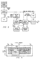
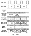
- FIG. 5 The block diagram of the OSD coprocessor is shown figure 5:
- Line counter The pixel and line counter receives the pixel clock, generate X, Y that represent the pixel position on the screen and synchronization signals Hsyn and Vsync to control the screen display.
- Windows Controller contains the positions X and Y of each windows to be displayed on the screen. The controller compares X, Y position, and indicates to the display controller each window transition and window number.
- Display controller For each new window transition the display controller read the new attribute from the attribute memory. It generates an address for the display memory and load the Fifo with a new block of data. It generate the attribute for the current window to the Decoder.
- Decoder For each pixel the decoder extracts from the Fifo the number of bits corresponding to the current pixel to be displayed. It transform data bit in pixel.
- Each hardware window has the following attributes:
- window position any even pixel horizontal position on screen; windows with decimated video have to start from an even numbered video line also
- window size from 2 to 720 pixel wide (even values only) and 1 to 576 lines
- bitmap resolution 1, 2, 4, and 8 bits per pixel
- the figure 6 shows an example of display of two overlapped windows.
- the window 2 on back is a bit map with 16 colors per pixel. Each pixel require 4-bits into the frame memory to define the code of the color.
- the window 1 on top is a bit map with 2 colors per pixel. Each pixel require 1-bits into the frame memory to define the code of the color.
- the position and dimension of the windows 1 is given by the attributes X_10, X_11, Y_10, Y_11. Horizontally the number of pixel is: X_11 - X_10. Vertically the number of lines is: Y_11 - Y_10: Same for window 2 with X_20, X_21, Y_20 and Y_21.
- the display controller access sequentially the display memory (figure 7) from the first word containing the pixel X_20, X_21 to the last word containing the pixel X_11, Y_11. Details of the line 20 is shown figure 7.
- the line begin with pixels of the window 2, window 1 start in X-10, Pa is the last pixel of window 2 with 4-bit per pixel, Pb is the first pixel of window 1 and use 1-bit per pixel. Window 1 end on Pc and window 1 restart in Pd until pixel position X_21.
- the same word contain pixels of window 1 and 2.
- the window controller detect the transition between Pa and Pb and control the data processing algorithm after Fifo access.
- the pixel selector and multiplex is the input of the decoder block shown figure 5. It receive the outputs of the Fifo and the windows attributes and control signals from the display controller.
- the basic function is to transform data stored into the frame memory in pixel.
- Pixel_Mux[7:0] is the address of the CLUT (Color Look Up Table). For graphic or still video picture the output is one color component.
- Pixel_Mux[7:0] output is produced by bits coming from the Fifo and bits from attribute memory.
- the first stage select one of the five bytes F[31:24], F23:16], F[15:8], F[7:0] and F[6:0] delayed by one clock sample.
- the second stage is a half barrel shifter that allows to shift right a 15-bit input data by 0 to 7 position.
- the output of the barrel shifter position the LSB of the code of the pixel to be displayed in Bs[0].
- the pixel counter provide the control signals for the multiplexor and barrel shifter.
- Table 2a shows the effect of the control Mux_S[1:0] on the bytes selection and 2b the output of the barrel shifter in function of Bs_S[2:0].
- the table 2c combine the table 2a and 2b and shows the bits of the Fifo selected at the output of the barrel shifter in function of the 5_bit pixel counter.
- Bp[3:0] 0000: The current window is empty and contain 0_bit per pixel or color component.
- Pm[7:0] is equal to Base[7:0] stored into the attribute register. In bit-map mode the Base[7:0] select one of the 256 colors of the CLUT as a background color.
- Bp[3:0] 0001:
- the current window contain 1_bit per pixel or color component.
- Pm[7:0] is equal to Base[7:1] concatenated with Bs[0] from the barrel shifter.
- the Base[7:1] is the base address of a set of 2_colors of the 256 colors CLUT.
- Bp[3:0] 0011:
- the current window contain 2_bit per pixel or color component.
- Pm[7:0] is equal to Base[7:2] concatenated with Bs[1:0] from the barrel shifter.
- the Base[7:2] is the base address of a set of 4_colors of the 256 colors CLUT.
- Bp[3:0] 0111:
- the current window contain 4_bit per pixel or color component.
- Pm[7:0] is equal to Base[7:4] concatenated with Bs[3:0] from the barrel shifter.
- the Base[7:4] is the base address of a set of 16_colors of the 256 colors CLUT.
- Bp[3:0] 1111:
- the current window contain 8_bit per pixel or color component.
- Pm[7:0] is equal to Bs[7:0] from the barrel shifter.
- bit-map mode the 256 colors CLUT are used.
- Each address clock signal generated by the pixel counter a new 32-bit word F[31:0] is sent to the pixel selector.
- the attribute memory contain the attributes of the windows to be displayed during the current frame.
- the attributes that control the pixel selector and multiplex are:
- Display mode bit-map, graphic, still video or empty.
- Number of bit per pixel or color component 0, 1, 2, 4 or 8 bits.
- the attribute register contain the attribute of the current window.
- the attribute clock transfers the content of attribute memory to the register when the window change.
- the window controller is composed of a content addressable memory CAM, flip flop and priority encoder.
- the CAM contain the attributes of position and size of the windows to be displayed on the current frame.
- the figure 9 shows a 32 words CAM. Each window require 4 words that indicate horizontally the coordinates of the first and last pixel and vertically the coordinates of the first and last line.
- a 32_words CAM support 8 windows.
- the CAM compare the value of the pixel and line counters respectively X and Y.
- Y counter match a value Yn0
- Y counter match a value Yn1 the corresponding window end vertically, RS flip-flop Wn_Y is reset.
- Wn_Y and Wn_X are combined to indicate that the X, Y counter is into an active window.
- the indices "n” indicate the window number.
- the priority encoder indicate the display order on the screen.
- Outputs of priority encoder are hit and OSD_W, Hit generates the attribute clock and OSD_W the memory attribute address corresponding to the active window.
- the details of the CAM cell is shown figure 10.
- the cell contain 2 parts, a 6 Transistors RAM cell and a 4 transistors comparator.
- the CPU load the content of the CAM with the attributes of position of the windows, memory mode is selected. During the display the associative mode is selected.
- the line counter Y and pixel counter X are compared to the content of all Yn and Xn of the CAM. When X or Y is equal to one or several values the corresponding Match lines are active to set or reset a flip-flop.
- the figures 11, 12 and 13 correspond to the generation of the display and frame memory represented figures 6 and 7.
- the pixel Px of the window 1 is selected into the 32_bit word "m".
- the pixel counter is decrement by one each access.
- Pixel selector put Px at the output Bs[0].
- the current window attribute select 1_bit per pixel.
- the pixel multiplex selects Base[7:1] and concatenate with Px to form the output Pixel_Mux[7:0].
- Pixel_Mux[7:0] select 2 colors of the CLUT.
- Base[7:1] is the base address of the CLUT.
- Figure 12 shows the generation of a pixel Px for the window 2 that use 4_bits per pixel in bit-map mode.
- Pixel selector put Px at the output Bs[3:0].
- the pixel multiplex selects Base[7:4] and concatenate with Bs[3:0] to form the output Pixel_Mux[7:0] that select one of the 16 colors of the CLUT.
- Base[7:4] is the base address of the CLUT. 16 CLUT of 16 colors can be selected with the window attributes.
- Figure 13 shows a specific case of the window 2 where Pn+1 has its 2 msb bits into the word m+1 and 2 lsb into m+2.
- Word m+2 is currently selected at the output of the fifo and the 7 lsb bits of word m+1 are maintained into the 7_bit register F-1[6:0].
- Pixel selector take F-1[1:0] concatenated with F[31:30] to generate Bs[3:0].
- the corresponding timing is shown figure 14b.
- Pn+1 pixel counter equal 30.
- the barrel shifter output generate F-1[5:0] concatenated with F[31:30].
- the current fifo address is word m+2 and the Pixel_Mux output is Base[7:4] & F-1[1:0] & F[31:30].
- Pixel Pn+2 the pixel counter is decrement by 4, the pixel selector select the next 4_bits of word m+2.
- the window 1 is on top of window 2.
- the CAM of the window controller is loaded with window 1 attributes position on top of window 2.
- the window displayed on top has the lower indices.
- Pixel Pa is last pixel for this portion of window 2 into the frame memory, the next bits contain the code of color of window 1, the first bit is Pb.
- window controller that generate the attribute clock to change the current display attribute stored in a register (see timing figure 14a).
- the frame memory In bit-map mode the frame memory contain the code of the color, 1,2,4 or 8 bits per color depending of the attributes.
- the code of the color concatenated with the CLUT color base attribute select a color from the CLUT.
- the CLUT contain 3 color components, one component for Luma and two components for Chroma.
- the mode When the picture is empty the mode is bit-map with 0_bit per pixel. This mode is used to generate a window with a background color or a decimated motion video picture coming from the MPEG video decoder.
- the pixel selector allows to mix by hardware different mode of display.
- the objective of this disclosure is to protect the pixel selector and multiplex hardware, its control, the window controller, window attribute generation and the flow of data from the frame memory to the Pixel_Mux output in the different display modes for different resolution.
- the frame memory contain a description of the current displayed picture. The description is done sequentially starting from the first upper left corner of a window "n" to the last lower right corner of a window "m". Only the active windows need to be described, not the full screen, background color or motion video.
- the description is done pixel per pixel, the number of bit to describe one pixel can vary for each window.
- Each transition of window is indicated by the attributes of position stored into the CAM.
- the window controller select the attribute of the corresponding window in real time during display.
- the pixel selector select the number of bits corresponding to the current pixel to be displayed.
- the complementary bits to form the 8_bit pixel output are obtained by concatenation of selected data bits from the frame and window attribute from the attribute memory.
- the mode When the picture is empty the mode is bit-map with 0_bit per pixel. This mode is used to generate a window with a background color or a decimated motion video picture coming from the MPEG video decoder.
Abstract
Description
- This invention relates to an on-screen display system with variable resolution.
- Current OSD systems may employ multiple central processing units (CPUs) in order to successfully deal with and handle high speed digital bit streams, such as those associated with a digital television set-top box. Each such CPU requires at least its own working memory space. These systems are expensive and may require expensive high speed memories.
- The OSD co-processor of the present invention provides for OSD systems that overcome these and other shortcomings of existing OSD systems.
- The present invention provides an OSD co-processor that allows for an OSD system having simultaneous display on a display screen of combinations of bit-map, graphic, still video picture, motion video picture or background. A frame memory containing a page to be displayed is preferably located in an external memory, which is preferably SDRAM. The OSD co-processor includes a display controller, a FIFO, an attribute memory, a window controller, a decoder, and line and pixel counters; the co-processor may also include an address calculator. A display controller reads the frame memory block by block and transfers the data to a FIFO. For each pixel, the decoder reads the bits required to display the current pixel from the FIFO; the number of bits per pixel may vary during the display depending upon the mode. A pixel selector and its controller select the bits of data from the FIFO to form the current pixel.
- The present invention will now be further described, by way of example, with reference to the example with reference to the accompanying drawings in which:
- Figure 1 depicts a high level architectural diagram of an audio/video decoding system employing an OSD co-processor of the present for to displaying an OSD picture;
- Figure 2 depicts display modes of an OSD co-processor of the present invention and their associated memory requirements;
- Figure 3 depicts two representative OSD pictures generated by an OSD co-processor of the present invention;
- Figure 4 depicts how a CPU builds windows in a portion of its memory and the windows are used to build a frame in a frame memory which is displayed by an OSD co-processor of the present invention on a screen display;
- Figure 5 depicts a high level architectural block diagram of an OSD co-processor of the present invention and selected interconnections;
- Figure 6 depicts two windows having different color schemes that illustrate how an OSD co-processor of the present invention displays two overlapped windows;
- Figure 7 depicts how a portion of the windows of Figure 6 are stored in a frame memory;
- Figure 8 depicts in more detail selected portions of the blocks of Figure 5;
- Figure 9 depicts a portion of a window controller of the present invention;
- Figure 10 depicts portions of a memory cell and memory logic utilized in a window controller of the OSD co-processor of the present invention;
- Figures 11-13 depict the generation, assembly and display of portions of windows depicted in Figures 6 and 7;
- Figure 14a depicts representative window transition timings, such as those for Figures 6 and 7; and
- Figure 14b depicts representative pixel selection and multiplexer timings for Figure 13.
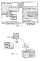
- The present invention provides an OSD co-processor for an OSD system. Figure 1 depicts one such OSD system.
- Figure 1 shows the global flow for decoding and displaying an OSD picture. The PSO buffer contains the coded picture, for example: Teletext data to be displayed within an OSD picture. The ARM CPU decodes (1) the Teletext data and builds (2) the OSD picture using a Bitblt hardware accelerator. The OSD controller reads (3) the OSD buffer and generates the OSD video that is mixed with MPEG video (4).
- Different modes may be displayed simultaneously on the screen: A bit-map window with 2 colors, a still video picture, a 256 colors graphic window, a decimated motion video picture and a Logo in true color. The OSD co-processor minimizes the memory required to display service information. The OSD uses a new hardware windowing technique to mix different modes of display such as: bit map with variable resolution, graphics, still video picture and decimated motion video.
- Figure 2 depicts the various modes of display supported by the OSD coprocessor of the present invention.
- More particularly, the OSD co-processor supports:
- 1) In a bit map the frame buffer contains the code of the color of each pixel to be displayed. The number of bits per pixel defines the number of the colors that can be displayed on screen. Two colors require 1-bit per pixel and 256 colors require 8-bits per pixel. This mode is used to display graphics and text. The code of the color addresses the Color Look Up Table (CLUT) that contains the three color components with 8-bits each.
- 2) Graphic plane, 4:4:4 mode, uses 8_bits per pixel for each color component R,G,B or Y,Cr,Cb. Each pixel requires 24-bits (16 million colors per pixel).
- 3) With the 4:2:2 mode the resolution of the chroma is divided horizontally by two. Each pixel has a luminance component Y and alternately a chrominance component Cr or Cb. This mode is used for video still or motion picture. Each pixel requires 16-bit.
- With the 4:2:0 mode the resolution of the chroma is divided by two horizontally and vertically. Each pixel has a luminance component Y and a chrominance component Cr and Cb for 4 pixels. This mode is used by the MPEG video decoder to the size of the memory required to store a video motion picture. Each pixel requires 12-bit. The chroma interpolator generates the 4:2:2 output format.
- Table 1 shows the number of bytes required to store a
full screen picture 720 pixels x 576 lines in different display modes for an OSD system that does not allow mixing of several modes of display in real time on the same screen. When one part of the screen requires 256 colors, the full screen must be 256 colors even if a part of the screen requires only 2 colors.
- However, the OSD coprocessor of the present invention can display several modes described above simultaneously on the same screen. Each part of the screen with different display mode uses a windows fully programmable in size, in position and priority level. The windows can be overlapped without limitations. The characteristic of each window is defined by a set of attributes stored into a SRAM. Those attributes are used to calculate the memory address in real time during display and to control the hardware display system.
-
Window size Number of bytes Window size Number of bytes 90 x 72 4:4:4 19 440 540 x 504 2-bit/pixel 68 040 360 x 288 1-bit/pixel 12 960 360 x 144 4-bit/pixel 25 920 360 x 144 4-bit/ pixel 25920 180 x 144 4:2:2 51840 720 x 576 Background 0 Total 110160 Total 93 960 720 x 576 Full screen 4:4:4 1 244 160 720 x 576 Full screen 4-bit/pixel 207 360 - Figure 3 shows typical OSD pictures. The left screen is composed of 5 OSD windows with different characteristics displayed on a full screen background color:
- a bit-map window 360 pixels by 288 lines with two colors that requires 1-bit per pixel,
- a bit-map window 360 pixels by 144 lines with 16 colors that requires 4-bit per pixel,
- a graphic window 90 pixels by 72 lines with 16 million colors that requires 24-bit per pixel,
- a still video picture window 180 pixels by 144 lines in 4:2:2 format using 24-bit per pixel,
- an MPEG motion video window 180 pixels by 144 lines in 4:2:0 format. The window size and position is generated by the OSD system. The MPEG video decoder generates the content of the window by decimation of the full screen picture.
- This OSD picture requires 110Kbytes memory. Without the OSD coprocessor the memory could be up to 1.24Meg bytes.
- The right screen shows an other picture composed of 2 OSD windows displayed over full screen motion video:
- a bit-map window 540 pixels by 504 lines with two colors that requires 1-bit per pixel. The background color is blended over motion video; and
- a bit-map window 360 pixels by 144 lines with 16 colors that requires 4-bit per pixel.
- The memory size is 93Kbytes with OSD coprocessor compare to 207Kbytes without OSD coprocessor.
- In frame mode (figure 4) CPU and frame uses different memory area. The CPU build the windows separately into the CPU memory, each windows has its own display attributes i.e. display mode, resolution. The new display picture is created by the CPU by coping sequentially with each segment of the
window window - The block diagram of the OSD coprocessor is shown figure 5:
- Line counter: The pixel and line counter receives the pixel clock, generate X, Y that represent the pixel position on the screen and synchronization signals Hsyn and Vsync to control the screen display.
- Windows Controller: contains the positions X and Y of each windows to be displayed on the screen. The controller compares X, Y position, and indicates to the display controller each window transition and window number.
- Address Calculator: Not used in frame mode.
- Display controller: For each new window transition the display controller read the new attribute from the attribute memory. It generates an address for the display memory and load the Fifo with a new block of data. It generate the attribute for the current window to the Decoder.
- Decoder: For each pixel the decoder extracts from the Fifo the number of bits corresponding to the current pixel to be displayed. It transform data bit in pixel.
- Display modes: empty window for decimated video. Bitmap, YCrCb 4:4:4 graphics component, YCrCb 4:2:2 CCIR 601 component and background color.
- Supports blending of bitmap, YCrCb 4:4:4, or YCrCb 4:2:2 with motion video and with an empty window
- Supports window mode and color mode blending
- Provides a programmable 256 entries Color Look Up table
- Outputs motion video for mixture with OSD in a programmable 422 or 444 digital component format
- Provides motion video or mixture with OSD to the on-chip NTSC/PAL encoder
- Each hardware window has the following attributes:
- window position: any even pixel horizontal position on screen; windows with decimated video have to start from an even numbered video line also
- window size: from 2 to 720 pixel wide (even values only) and 1 to 576 lines
- window base address
- data format: bitmap, YCrCb 4:4:4, YCrCb 4:2:2, and empty
- bitmap resolution: 1, 2, 4, and 8 bits per pixel
- full or half resolution for bitmap and YCrCb 4:4:4 windows
- bitmap color palette base address
- blend enable flag
- 4 or 16 levels of blending
- transparency enable flag for YCrCb 4:4:4 and YCrCb 4:2:2
- output channel control
- The figure 6 shows an example of display of two overlapped windows. The
window 2 on back is a bit map with 16 colors per pixel. Each pixel require 4-bits into the frame memory to define the code of the color. Thewindow 1 on top is a bit map with 2 colors per pixel. Each pixel require 1-bits into the frame memory to define the code of the color. The position and dimension of thewindows 1 is given by the attributes X_10, X_11, Y_10, Y_11. Horizontally the number of pixel is: X_11 - X_10. Vertically the number of lines is: Y_11 - Y_10: Same forwindow 2 with X_20, X_21, Y_20 and Y_21. - The display controller access sequentially the display memory (figure 7) from the first word containing the pixel X_20, X_21 to the last word containing the pixel X_11, Y_11. Details of the line 20 is shown figure 7. The line begin with pixels of the
window 2,window 1 start in X-10, Pa is the last pixel ofwindow 2 with 4-bit per pixel, Pb is the first pixel ofwindow 1 and use 1-bit per pixel.Window 1 end on Pc andwindow 1 restart in Pd until pixel position X_21. - The same word contain pixels of
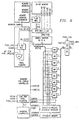
window - The pixel selector and multiplex is the input of the decoder block shown figure 5. It receive the outputs of the Fifo and the windows attributes and control signals from the display controller. The basic function is to transform data stored into the frame memory in pixel. In case of bit map display (figure 8) the output, Pixel_Mux[7:0] is the address of the CLUT (Color Look Up Table). For graphic or still video picture the output is one color component. Pixel_Mux[7:0] output is produced by bits coming from the Fifo and bits from attribute memory.
- Receive 32-bit data from the Fifo outputs F[31:0]. The first stage select one of the five bytes F[31:24], F23:16], F[15:8], F[7:0] and F[6:0] delayed by one clock sample. The second stage is a half barrel shifter that allows to shift right a 15-bit input data by 0 to 7 position. The output of the barrel shifter position the LSB of the code of the pixel to be displayed in Bs[0]. The pixel counter provide the control signals for the multiplexor and barrel shifter. Table 2a shows the effect of the control Mux_S[1:0] on the bytes selection and 2b the output of the barrel shifter in function of Bs_S[2:0]. The table 2c combine the table 2a and 2b and shows the bits of the Fifo selected at the output of the barrel shifter in function of the 5_bit pixel counter.
- Receive data Bs[7:0] from the barrel shifter and Base[7:0] from the attribute register. It is controlled by, 4 control bits coming from the attribute register, Cursor and default signals from display controller as shown table 2d.

- Default: When active Pm[7:0] is equal to the 8-bit default color provided by the general control register of the display controller. No data is read from the Fifo.
- Cursor: When active Pm[7:0] is equal to the 8-bit cursor color provided by the general control register of the display controller. No data is read from the Fifo.
- Bp[3:0]=0000: The current window is empty and contain 0_bit per pixel or color component. Pm[7:0] is equal to Base[7:0] stored into the attribute register. In bit-map mode the Base[7:0] select one of the 256 colors of the CLUT as a background color.
- Bp[3:0]=0001: The current window contain 1_bit per pixel or color component. Pm[7:0] is equal to Base[7:1] concatenated with Bs[0] from the barrel shifter. In bit-map mode the Base[7:1] is the base address of a set of 2_colors of the 256 colors CLUT.
- Bp[3:0]=0011: The current window contain 2_bit per pixel or color component. Pm[7:0] is equal to Base[7:2] concatenated with Bs[1:0] from the barrel shifter. In bit-map mode the Base[7:2] is the base address of a set of 4_colors of the 256 colors CLUT.
- Bp[3:0]=0111: The current window contain 4_bit per pixel or color component. Pm[7:0] is equal to Base[7:4] concatenated with Bs[3:0] from the barrel shifter. In bit-map mode the Base[7:4] is the base address of a set of 16_colors of the 256 colors CLUT.
- Bp[3:0]=1111: The current window contain 8_bit per pixel or color component. Pm[7:0] is equal to Bs[7:0] from the barrel shifter. In bit-map mode the 256 colors CLUT are used.
- Provide the control for the pixel selector Mux_S[1:0] concatenated with Bs_S[2:0]. Each beginning of frame the pixel counter is reset. It is decremented by 0, 1, 2, 4 or 8 depending of the current window attribute. Address clock signal is generated when the counter cross zero.
- It generate the read address for the Fifo. Each address clock signal generated by the pixel counter a new 32-bit word F[31:0] is sent to the pixel selector.
- The attribute memory contain the attributes of the windows to be displayed during the current frame. The attributes that control the pixel selector and multiplex are:
- Display mode: bit-map, graphic, still video or empty.
- Number of bit per pixel or color component: 0, 1, 2, 4 or 8 bits.
- The bit-map CLUT base address.
- The attribute register contain the attribute of the current window. The attribute clock transfers the content of attribute memory to the register when the window change.
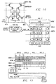
- The window controller is composed of a content addressable memory CAM, flip flop and priority encoder. The CAM contain the attributes of position and size of the windows to be displayed on the current frame. The figure 9 shows a 32 words CAM. Each window require 4 words that indicate horizontally the coordinates of the first and last pixel and vertically the coordinates of the first and last line. A
32_words CAM support 8 windows. - The CAM compare the value of the pixel and line counters respectively X and Y. When Y counter match a value Yn0, a new window start vertically, the corresponding RS flip-flop is set Wn_Y=1. When Y counter match a value Yn1, the corresponding window end vertically, RS flip-flop Wn_Y is reset. The process is the same horizontally. Wn_Y and Wn_X are combined to indicate that the X, Y counter is into an active window. The indices "n" indicate the window number. Several windows can be overlapped, the priority encoder indicate the display order on the screen. The indices "n=0" correspond to the cursor that must be always on top. Outputs of priority encoder are hit and OSD_W, Hit generates the attribute clock and OSD_W the memory attribute address corresponding to the active window.
- The details of the CAM cell is shown figure 10. The cell contain 2 parts, a 6 Transistors RAM cell and a 4 transistors comparator. The CPU load the content of the CAM with the attributes of position of the windows, memory mode is selected. During the display the associative mode is selected. The line counter Y and pixel counter X are compared to the content of all Yn and Xn of the CAM. When X or Y is equal to one or several values the corresponding Match lines are active to set or reset a flip-flop.
- The figures 11, 12 and 13 correspond to the generation of the display and frame memory represented figures 6 and 7.
- Figure 11, the pixel Px of the
window 1 is selected into the 32_bit word "m". The pixel counter is decrement by one each access. Pixel selector put Px at the output Bs[0]. The current window attribute select 1_bit per pixel. The pixel multiplex selects Base[7:1] and concatenate with Px to form the output Pixel_Mux[7:0]. In bit-map mode Pixel_Mux[7:0] select 2 colors of the CLUT. Base[7:1] is the base address of the CLUT. - Figure 12 shows the generation of a pixel Px for the
window 2 that use 4_bits per pixel in bit-map mode. Pixel selector put Px at the output Bs[3:0]. The pixel multiplex selects Base[7:4] and concatenate with Bs[3:0] to form the output Pixel_Mux[7:0] that select one of the 16 colors of the CLUT. Base[7:4] is the base address of the CLUT. 16 CLUT of 16 colors can be selected with the window attributes. - Figure 13 shows a specific case of the
window 2 where Pn+1 has its 2 msb bits into the word m+1 and 2 lsb into m+2. Word m+2 is currently selected at the output of the fifo and the 7 lsb bits of word m+1 are maintained into the 7_bit register F-1[6:0]. Pixel selector take F-1[1:0] concatenated with F[31:30] to generate Bs[3:0]. The corresponding timing is shown figure 14b. At Pn+1 pixel counter equal 30. The barrel shifter output generate F-1[5:0] concatenated with F[31:30]. The current fifo address is word m+2 and the Pixel_Mux output is Base[7:4] & F-1[1:0] & F[31:30]. Pixel Pn+2 the pixel counter is decrement by 4, the pixel selector select the next 4_bits of word m+2. - Figure 6 the
window 1 is on top ofwindow 2. The CAM of the window controller is loaded withwindow 1 attributes position on top ofwindow 2. The window displayed on top has the lower indices. Pixel Pa is last pixel for this portion ofwindow 2 into the frame memory, the next bits contain the code of color ofwindow 1, the first bit is Pb. During thesame line window 1 end in Pc andwindow 2 restart in Pd. Each of this window transitions are detected by the window controller that generate the attribute clock to change the current display attribute stored in a register (see timing figure 14a). For Pa-1 and Pa the Pixel counter is decrement by 4 each pixel and after attribute clock Bp[3:0]=1 (figure 8) decrement the counter by 1 each pixel. - In bit-map mode the frame memory contain the code of the color, 1,2,4 or 8 bits per color depending of the attributes. The code of the color concatenated with the CLUT color base attribute select a color from the CLUT. The CLUT contain 3 color components, one component for Luma and two components for Chroma.
- When the current window is graphic, the CLUT is not used. Each pixel there is 3 access identical to the bit-map mode to extract the 3 colors components from the frame memory. There is 3 access during a pixel.
- In still video picture the CLUT is not used. Still video reduce Chroma bandwidth. Each pixel there is 2 access identical to the bit-map mode to extract one Luma components and chroma component Cr or Cb alternately each pixel from the frame memory.
- When the picture is empty the mode is bit-map with 0_bit per pixel. This mode is used to generate a window with a background color or a decimated motion video picture coming from the MPEG video decoder.
- The pixel selector allows to mix by hardware different mode of display. The objective of this disclosure is to protect the pixel selector and multiplex hardware, its control, the window controller, window attribute generation and the flow of data from the frame memory to the Pixel_Mux output in the different display modes for different resolution.
- The frame memory contain a description of the current displayed picture. The description is done sequentially starting from the first upper left corner of a window "n" to the last lower right corner of a window "m". Only the active windows need to be described, not the full screen, background color or motion video.
- The description is done pixel per pixel, the number of bit to describe one pixel can vary for each window.
- Each transition of window is indicated by the attributes of position stored into the CAM. The window controller select the attribute of the corresponding window in real time during display.
- The pixel selector select the number of bits corresponding to the current pixel to be displayed.
- The complementary bits to form the 8_bit pixel output are obtained by concatenation of selected data bits from the frame and window attribute from the attribute memory.
- When the current window is bit-map Pixel_Mux output select a color of the CLUT. The CLUT contain the 3 colors component.
- When the current window is graphic, the CLUT is not used. Each pixel there is 3 access identical to the bit-map mode to extract the 3 colors components from the frame memory.
- In still video picture the CLUT is not used. Each pixel there is 2 access identical to the bit-map mode to extract the 2 colors components from the frame memory. Luma is extracted each pixel and chroma component Cr and Cb alternately each pixel.
- When the picture is empty the mode is bit-map with 0_bit per pixel. This mode is used to generate a window with a background color or a decimated motion video picture coming from the MPEG video decoder.
Claims (2)
- An on-screen display co-processor, comprising:a FIFO;a decoder coupled to said FIFO;a display controller coupled to said FIFO and decoder;a window controller coupled to said display controller;line and pixel counters coupled to said windows controller; andan attribute memory coupled to said display controller.
- A window controller, comprising:a content addressable memory for storing data corresponding to window position and size and for comparing pixel and line counter data with such data,at least one flip-flop coupled to said memory for indicating whether a window is active or not active, anda priority encoder coupled to said flip-flop for selecting the display order of any active windows.
Applications Claiming Priority (2)
| Application Number | Priority Date | Filing Date | Title |
|---|---|---|---|
| US3010796P | 1996-11-01 | 1996-11-01 | |
| US30107P | 1996-11-01 |
Publications (3)
| Publication Number | Publication Date |
|---|---|
| EP0840276A2 true EP0840276A2 (en) | 1998-05-06 |
| EP0840276A3 EP0840276A3 (en) | 1999-06-23 |
| EP0840276B1 EP0840276B1 (en) | 2002-10-16 |
Family
ID=21852549
Family Applications (1)
| Application Number | Title | Priority Date | Filing Date |
|---|---|---|---|
| EP97119122A Expired - Lifetime EP0840276B1 (en) | 1996-11-01 | 1997-11-03 | Window processing in an on screen display system |
Country Status (4)
| Country | Link |
|---|---|
| EP (1) | EP0840276B1 (en) |
| JP (1) | JPH10187126A (en) |
| KR (1) | KR19980042031A (en) |
| DE (1) | DE69716376T2 (en) |
Cited By (13)
| Publication number | Priority date | Publication date | Assignee | Title |
|---|---|---|---|---|
| EP1145218A2 (en) * | 1998-11-09 | 2001-10-17 | Broadcom Corporation | Display system for blending graphics and video data |
| US6661426B1 (en) | 1999-09-25 | 2003-12-09 | Koninklijke Philips Electronics N.V. | User interface generation |
| US6768774B1 (en) | 1998-11-09 | 2004-07-27 | Broadcom Corporation | Video and graphics system with video scaling |
| US6781601B2 (en) | 1999-11-09 | 2004-08-24 | Broadcom Corporation | Transport processor |
| US6798420B1 (en) | 1998-11-09 | 2004-09-28 | Broadcom Corporation | Video and graphics system with a single-port RAM |
| WO2005015912A2 (en) * | 2003-08-08 | 2005-02-17 | Maven Networks, Inc. | System and method of integrating video content with interactive elements |
| US7659900B2 (en) | 1998-11-09 | 2010-02-09 | Broadcom Corporation | Video and graphics system with parallel processing of graphics windows |
| US7667710B2 (en) | 2003-04-25 | 2010-02-23 | Broadcom Corporation | Graphics display system with line buffer control scheme |
| US7667715B2 (en) | 1999-11-09 | 2010-02-23 | Broadcom Corporation | Video, audio and graphics decode, composite and display system |
| US7848430B2 (en) | 1999-11-09 | 2010-12-07 | Broadcom Corporation | Video and graphics system with an MPEG video decoder for concurrent multi-row decoding |
| US8063916B2 (en) * | 2003-10-22 | 2011-11-22 | Broadcom Corporation | Graphics layer reduction for video composition |
| US8913667B2 (en) | 1999-11-09 | 2014-12-16 | Broadcom Corporation | Video decoding system having a programmable variable-length decoder |
| CN106534939A (en) * | 2016-10-09 | 2017-03-22 | 北京金山安全软件有限公司 | Multi-video preview method and device and electronic equipment |
Families Citing this family (7)
| Publication number | Priority date | Publication date | Assignee | Title |
|---|---|---|---|---|
| US6661422B1 (en) | 1998-11-09 | 2003-12-09 | Broadcom Corporation | Video and graphics system with MPEG specific data transfer commands |
| US6573905B1 (en) | 1999-11-09 | 2003-06-03 | Broadcom Corporation | Video and graphics system with parallel processing of graphics windows |
| US7982740B2 (en) | 1998-11-09 | 2011-07-19 | Broadcom Corporation | Low resolution graphics mode support using window descriptors |
| US6538656B1 (en) | 1999-11-09 | 2003-03-25 | Broadcom Corporation | Video and graphics system with a data transport processor |
| JP4843872B2 (en) | 2001-07-03 | 2011-12-21 | 船井電機株式会社 | Television receiver |
| JP4169340B2 (en) * | 2002-11-25 | 2008-10-22 | カシオ計算機株式会社 | Output signal generation circuit for display panel, digital camera, and output signal generation method for display panel |
| KR100597406B1 (en) | 2004-06-29 | 2006-07-06 | 삼성전자주식회사 | Settop box which is inputted for animation in On Screen Display and method thereof |
Citations (10)
| Publication number | Priority date | Publication date | Assignee | Title |
|---|---|---|---|---|
| WO1986005910A1 (en) * | 1985-04-03 | 1986-10-09 | British Telecommunications Public Limited Company | Video display apparatus |
| EP0276884A1 (en) * | 1987-01-27 | 1988-08-03 | Philips Composants | Device for synthesizing images |
| EP0280582A2 (en) * | 1987-02-27 | 1988-08-31 | Axiom Innovation Limited | Improvements in computer graphics systems |
| EP0384419A2 (en) * | 1989-02-24 | 1990-08-29 | International Business Machines Corporation | Color-television window for a video-display unit |
| WO1991018353A1 (en) * | 1990-05-14 | 1991-11-28 | Chips And Technologies, Inc. | Display list processor for terminal controller |
| EP0601647A1 (en) * | 1992-12-11 | 1994-06-15 | Koninklijke Philips Electronics N.V. | System for combining multiple-format multiple-source video signals |
| EP0615223A1 (en) * | 1993-03-10 | 1994-09-14 | AT&T Corp. | Method and apparatus for the coding and display of overlapping windows with transparency |
| EP0724249A1 (en) * | 1995-01-30 | 1996-07-31 | International Business Machines Corporation | Method for identifying video pixel data format in a mixed format data stream |
| US5604514A (en) * | 1994-01-03 | 1997-02-18 | International Business Machines Corporation | Personal computer with combined graphics/image display system having pixel mode frame buffer interpretation |
| WO1997016788A1 (en) * | 1995-11-03 | 1997-05-09 | Sierra Semiconductor Corporation | Split video architecture for personal computers |
-
1997
- 1997-11-01 KR KR1019970057602A patent/KR19980042031A/en not_active Application Discontinuation
- 1997-11-03 EP EP97119122A patent/EP0840276B1/en not_active Expired - Lifetime
- 1997-11-03 DE DE69716376T patent/DE69716376T2/en not_active Expired - Lifetime
- 1997-11-04 JP JP9339255A patent/JPH10187126A/en active Pending
Patent Citations (10)
| Publication number | Priority date | Publication date | Assignee | Title |
|---|---|---|---|---|
| WO1986005910A1 (en) * | 1985-04-03 | 1986-10-09 | British Telecommunications Public Limited Company | Video display apparatus |
| EP0276884A1 (en) * | 1987-01-27 | 1988-08-03 | Philips Composants | Device for synthesizing images |
| EP0280582A2 (en) * | 1987-02-27 | 1988-08-31 | Axiom Innovation Limited | Improvements in computer graphics systems |
| EP0384419A2 (en) * | 1989-02-24 | 1990-08-29 | International Business Machines Corporation | Color-television window for a video-display unit |
| WO1991018353A1 (en) * | 1990-05-14 | 1991-11-28 | Chips And Technologies, Inc. | Display list processor for terminal controller |
| EP0601647A1 (en) * | 1992-12-11 | 1994-06-15 | Koninklijke Philips Electronics N.V. | System for combining multiple-format multiple-source video signals |
| EP0615223A1 (en) * | 1993-03-10 | 1994-09-14 | AT&T Corp. | Method and apparatus for the coding and display of overlapping windows with transparency |
| US5604514A (en) * | 1994-01-03 | 1997-02-18 | International Business Machines Corporation | Personal computer with combined graphics/image display system having pixel mode frame buffer interpretation |
| EP0724249A1 (en) * | 1995-01-30 | 1996-07-31 | International Business Machines Corporation | Method for identifying video pixel data format in a mixed format data stream |
| WO1997016788A1 (en) * | 1995-11-03 | 1997-05-09 | Sierra Semiconductor Corporation | Split video architecture for personal computers |
Cited By (32)
| Publication number | Priority date | Publication date | Assignee | Title |
|---|---|---|---|---|
| US8390635B2 (en) | 1998-11-09 | 2013-03-05 | Broadcom Corporation | Graphics accelerator |
| US7991049B2 (en) | 1998-11-09 | 2011-08-02 | Broadcom Corporation | Video and graphics system with video scaling |
| EP1365385A3 (en) * | 1998-11-09 | 2008-07-30 | Broadcom Corporation | Graphics display system with processing of graphics layers, alpha blending and composition with video data |
| US6721837B2 (en) | 1998-11-09 | 2004-04-13 | Broadcom Corporation | Graphics display system with unified memory architecture |
| US6731295B1 (en) | 1998-11-09 | 2004-05-04 | Broadcom Corporation | Graphics display system with window descriptors |
| US6738072B1 (en) | 1998-11-09 | 2004-05-18 | Broadcom Corporation | Graphics display system with anti-flutter filtering and vertical scaling feature |
| US7659900B2 (en) | 1998-11-09 | 2010-02-09 | Broadcom Corporation | Video and graphics system with parallel processing of graphics windows |
| US6744472B1 (en) | 1998-11-09 | 2004-06-01 | Broadcom Corporation | Graphics display system with video synchronization feature |
| US6768774B1 (en) | 1998-11-09 | 2004-07-27 | Broadcom Corporation | Video and graphics system with video scaling |
| US9575665B2 (en) | 1998-11-09 | 2017-02-21 | Broadcom Corporation | Graphics display system with unified memory architecture |
| US6798420B1 (en) | 1998-11-09 | 2004-09-28 | Broadcom Corporation | Video and graphics system with a single-port RAM |
| US6819330B2 (en) | 1998-11-09 | 2004-11-16 | Broadcom Corporation | Graphics display System with color look-up table loading mechanism |
| US9077997B2 (en) | 1998-11-09 | 2015-07-07 | Broadcom Corporation | Graphics display system with unified memory architecture |
| US8493415B2 (en) | 1998-11-09 | 2013-07-23 | Broadcom Corporation | Graphics display system with video scaler |
| EP1145218A2 (en) * | 1998-11-09 | 2001-10-17 | Broadcom Corporation | Display system for blending graphics and video data |
| EP1365385A2 (en) * | 1998-11-09 | 2003-11-26 | Broadcom Corporation | Graphics display system with processing of graphics layers, alpha blending and composition with video data |
| EP1145218B1 (en) * | 1998-11-09 | 2004-05-19 | Broadcom Corporation | Display system for blending graphics and video data |
| US7920151B2 (en) | 1998-11-09 | 2011-04-05 | Broadcom Corporation | Graphics display system with video scaler |
| US7746354B2 (en) | 1998-11-09 | 2010-06-29 | Broadcom Corporation | Graphics display system with anti-aliased text and graphics feature |
| US7911483B1 (en) | 1998-11-09 | 2011-03-22 | Broadcom Corporation | Graphics display system with window soft horizontal scrolling mechanism |
| US6661426B1 (en) | 1999-09-25 | 2003-12-09 | Koninklijke Philips Electronics N.V. | User interface generation |
| US7848430B2 (en) | 1999-11-09 | 2010-12-07 | Broadcom Corporation | Video and graphics system with an MPEG video decoder for concurrent multi-row decoding |
| US7667715B2 (en) | 1999-11-09 | 2010-02-23 | Broadcom Corporation | Video, audio and graphics decode, composite and display system |
| US8913667B2 (en) | 1999-11-09 | 2014-12-16 | Broadcom Corporation | Video decoding system having a programmable variable-length decoder |
| US6781601B2 (en) | 1999-11-09 | 2004-08-24 | Broadcom Corporation | Transport processor |
| US9668011B2 (en) | 2001-02-05 | 2017-05-30 | Avago Technologies General Ip (Singapore) Pte. Ltd. | Single chip set-top box system |
| US7667710B2 (en) | 2003-04-25 | 2010-02-23 | Broadcom Corporation | Graphics display system with line buffer control scheme |
| WO2005015912A3 (en) * | 2003-08-08 | 2005-09-09 | Maven Networks Inc | System and method of integrating video content with interactive elements |
| WO2005015912A2 (en) * | 2003-08-08 | 2005-02-17 | Maven Networks, Inc. | System and method of integrating video content with interactive elements |
| US8063916B2 (en) * | 2003-10-22 | 2011-11-22 | Broadcom Corporation | Graphics layer reduction for video composition |
| CN106534939A (en) * | 2016-10-09 | 2017-03-22 | 北京金山安全软件有限公司 | Multi-video preview method and device and electronic equipment |
| CN106534939B (en) * | 2016-10-09 | 2019-07-05 | 北京金山安全软件有限公司 | Multi-video preview method and device and electronic equipment |
Also Published As
| Publication number | Publication date |
|---|---|
| EP0840276B1 (en) | 2002-10-16 |
| DE69716376T2 (en) | 2003-06-05 |
| DE69716376D1 (en) | 2002-11-21 |
| JPH10187126A (en) | 1998-07-14 |
| KR19980042031A (en) | 1998-08-17 |
| EP0840276A3 (en) | 1999-06-23 |
Similar Documents
| Publication | Publication Date | Title |
|---|---|---|
| US6452641B1 (en) | Method and apparatus for providing and on-screen display with variable resolution capability | |
| EP0840276B1 (en) | Window processing in an on screen display system | |
| EP0840277A2 (en) | Window processing in an on screen display system | |
| JP3818662B2 (en) | Image processing system having a single frame buffer | |
| US5227863A (en) | Programmable digital video processing system | |
| US5625379A (en) | Video processing apparatus systems and methods | |
| US6466220B1 (en) | Graphics engine architecture | |
| US5896140A (en) | Method and apparatus for simultaneously displaying graphics and video data on a computer display | |
| US5517612A (en) | Device for scaling real-time image frames in multi-media workstations | |
| US5808630A (en) | Split video architecture for personal computers | |
| US8199154B2 (en) | Low resolution graphics mode support using window descriptors | |
| US5557302A (en) | Method and apparatus for displaying video data on a computer display | |
| JPH06303423A (en) | Coupling system for composite mode-composite signal source picture signal | |
| EP0840505A2 (en) | System to multiplex and blend graphics OSD and motion video pictures for digital television | |
| US6424342B1 (en) | Decompressing and compositing graphical image data | |
| US5010406A (en) | Apparatus for receiving character multiplex broadcasting | |
| US7164431B1 (en) | System and method for mixing graphics and text in an on-screen display application | |
| EP0951694B1 (en) | Method and apparatus for using interpolation line buffers as pixel look up tables | |
| US7893943B1 (en) | Systems and methods for converting a pixel rate of an incoming digital image frame | |
| JP3542690B2 (en) | Video graphics equipment for television | |
| GB2267202A (en) | Multiple buffer processing architecture for integrated display of video and graphics with independent color depth | |
| US6118494A (en) | Apparatus and method for generating on-screen-display messages using true color mode | |
| US7227584B2 (en) | Video signal processing system | |
| JP3014935B2 (en) | Interlaced scanning on-screen display circuit | |
| JPH0213990A (en) | Graphic memory apparatus |
Legal Events
| Date | Code | Title | Description |
|---|---|---|---|
| PUAI | Public reference made under article 153(3) epc to a published international application that has entered the european phase |
Free format text: ORIGINAL CODE: 0009012 |
|
| AK | Designated contracting states |
Kind code of ref document: A2 Designated state(s): DE FR GB IT NL |
|
| PUAL | Search report despatched |
Free format text: ORIGINAL CODE: 0009013 |
|
| AK | Designated contracting states |
Kind code of ref document: A3 Designated state(s): AT BE CH DE DK ES FI FR GB GR IE IT LI LU MC NL PT SE |
|
| 17P | Request for examination filed |
Effective date: 19991223 |
|
| AKX | Designation fees paid |
Free format text: DE FR GB IT NL |
|
| 17Q | First examination report despatched |
Effective date: 20000313 |
|
| GRAG | Despatch of communication of intention to grant |
Free format text: ORIGINAL CODE: EPIDOS AGRA |
|
| GRAG | Despatch of communication of intention to grant |
Free format text: ORIGINAL CODE: EPIDOS AGRA |
|
| GRAH | Despatch of communication of intention to grant a patent |
Free format text: ORIGINAL CODE: EPIDOS IGRA |
|
| GRAH | Despatch of communication of intention to grant a patent |
Free format text: ORIGINAL CODE: EPIDOS IGRA |
|
| GRAA | (expected) grant |
Free format text: ORIGINAL CODE: 0009210 |
|
| AK | Designated contracting states |
Kind code of ref document: B1 Designated state(s): DE FR GB IT NL |
|
| PG25 | Lapsed in a contracting state [announced via postgrant information from national office to epo] |
Ref country code: NL Free format text: LAPSE BECAUSE OF FAILURE TO SUBMIT A TRANSLATION OF THE DESCRIPTION OR TO PAY THE FEE WITHIN THE PRESCRIBED TIME-LIMIT Effective date: 20021016 Ref country code: IT Free format text: LAPSE BECAUSE OF FAILURE TO SUBMIT A TRANSLATION OF THE DESCRIPTION OR TO PAY THE FEE WITHIN THE PRESCRIBED TIME-LIMIT;WARNING: LAPSES OF ITALIAN PATENTS WITH EFFECTIVE DATE BEFORE 2007 MAY HAVE OCCURRED AT ANY TIME BEFORE 2007. THE CORRECT EFFECTIVE DATE MAY BE DIFFERENT FROM THE ONE RECORDED. Effective date: 20021016 |
|
| REG | Reference to a national code |
Ref country code: GB Ref legal event code: FG4D |
|
| REF | Corresponds to: |
Ref document number: 69716376 Country of ref document: DE Date of ref document: 20021121 |
|
| NLV1 | Nl: lapsed or annulled due to failure to fulfill the requirements of art. 29p and 29m of the patents act | ||
| ET | Fr: translation filed | ||
| PLBE | No opposition filed within time limit |
Free format text: ORIGINAL CODE: 0009261 |
|
| STAA | Information on the status of an ep patent application or granted ep patent |
Free format text: STATUS: NO OPPOSITION FILED WITHIN TIME LIMIT |
|
| 26N | No opposition filed |
Effective date: 20030717 |
|
| PGFP | Annual fee paid to national office [announced via postgrant information from national office to epo] |
Ref country code: DE Payment date: 20121130 Year of fee payment: 16 Ref country code: FR Payment date: 20121113 Year of fee payment: 16 |
|
| PGFP | Annual fee paid to national office [announced via postgrant information from national office to epo] |
Ref country code: GB Payment date: 20121025 Year of fee payment: 16 |
|
| GBPC | Gb: european patent ceased through non-payment of renewal fee |
Effective date: 20131103 |
|
| REG | Reference to a national code |
Ref country code: FR Ref legal event code: ST Effective date: 20140731 |
|
| REG | Reference to a national code |
Ref country code: DE Ref legal event code: R119 Ref document number: 69716376 Country of ref document: DE Effective date: 20140603 |
|
| PG25 | Lapsed in a contracting state [announced via postgrant information from national office to epo] |
Ref country code: DE Free format text: LAPSE BECAUSE OF NON-PAYMENT OF DUE FEES Effective date: 20140603 |
|
| PG25 | Lapsed in a contracting state [announced via postgrant information from national office to epo] |
Ref country code: FR Free format text: LAPSE BECAUSE OF NON-PAYMENT OF DUE FEES Effective date: 20131202 Ref country code: GB Free format text: LAPSE BECAUSE OF NON-PAYMENT OF DUE FEES Effective date: 20131103 |