EP0861017A2 - Photodetector of liquid crystal display and luminance control device using the same - Google Patents
Photodetector of liquid crystal display and luminance control device using the same Download PDFInfo
- Publication number
- EP0861017A2 EP0861017A2 EP98300672A EP98300672A EP0861017A2 EP 0861017 A2 EP0861017 A2 EP 0861017A2 EP 98300672 A EP98300672 A EP 98300672A EP 98300672 A EP98300672 A EP 98300672A EP 0861017 A2 EP0861017 A2 EP 0861017A2
- Authority
- EP
- European Patent Office
- Prior art keywords
- luminance
- liquid crystal
- light
- crystal display
- backlight
- Prior art date
- Legal status (The legal status is an assumption and is not a legal conclusion. Google has not performed a legal analysis and makes no representation as to the accuracy of the status listed.)
- Granted
Links
- 239000004973 liquid crystal related substance Substances 0.000 title claims abstract description 54
- 238000009792 diffusion process Methods 0.000 claims abstract description 6
- 230000005684 electric field Effects 0.000 claims description 6
- 238000000034 method Methods 0.000 claims description 4
- 230000005855 radiation Effects 0.000 claims description 4
- FPWNLURCHDRMHC-UHFFFAOYSA-N 4-chlorobiphenyl Chemical compound C1=CC(Cl)=CC=C1C1=CC=CC=C1 FPWNLURCHDRMHC-UHFFFAOYSA-N 0.000 description 6
- 230000000903 blocking effect Effects 0.000 description 5
- 230000035945 sensitivity Effects 0.000 description 5
- 238000001514 detection method Methods 0.000 description 3
- XOMKZKJEJBZBJJ-UHFFFAOYSA-N 1,2-dichloro-3-phenylbenzene Chemical compound ClC1=CC=CC(C=2C=CC=CC=2)=C1Cl XOMKZKJEJBZBJJ-UHFFFAOYSA-N 0.000 description 2
- 230000015556 catabolic process Effects 0.000 description 2
- 238000006731 degradation reaction Methods 0.000 description 2
- 238000010586 diagram Methods 0.000 description 2
- 230000000694 effects Effects 0.000 description 2
- XAGFODPZIPBFFR-UHFFFAOYSA-N aluminium Chemical compound [Al] XAGFODPZIPBFFR-UHFFFAOYSA-N 0.000 description 1
- 229910052782 aluminium Inorganic materials 0.000 description 1
- 230000008859 change Effects 0.000 description 1
- 230000003247 decreasing effect Effects 0.000 description 1
- 230000007613 environmental effect Effects 0.000 description 1
- 230000004048 modification Effects 0.000 description 1
- 238000012986 modification Methods 0.000 description 1
- 238000012544 monitoring process Methods 0.000 description 1
- 230000008569 process Effects 0.000 description 1
- 230000009467 reduction Effects 0.000 description 1
Images


Classifications
-
- G—PHYSICS
- G09—EDUCATION; CRYPTOGRAPHY; DISPLAY; ADVERTISING; SEALS
- G09G—ARRANGEMENTS OR CIRCUITS FOR CONTROL OF INDICATING DEVICES USING STATIC MEANS TO PRESENT VARIABLE INFORMATION
- G09G3/00—Control arrangements or circuits, of interest only in connection with visual indicators other than cathode-ray tubes
- G09G3/20—Control arrangements or circuits, of interest only in connection with visual indicators other than cathode-ray tubes for presentation of an assembly of a number of characters, e.g. a page, by composing the assembly by combination of individual elements arranged in a matrix no fixed position being assigned to or needed to be assigned to the individual characters or partial characters
- G09G3/34—Control arrangements or circuits, of interest only in connection with visual indicators other than cathode-ray tubes for presentation of an assembly of a number of characters, e.g. a page, by composing the assembly by combination of individual elements arranged in a matrix no fixed position being assigned to or needed to be assigned to the individual characters or partial characters by control of light from an independent source
- G09G3/3406—Control of illumination source
-
- G—PHYSICS
- G02—OPTICS
- G02F—OPTICAL DEVICES OR ARRANGEMENTS FOR THE CONTROL OF LIGHT BY MODIFICATION OF THE OPTICAL PROPERTIES OF THE MEDIA OF THE ELEMENTS INVOLVED THEREIN; NON-LINEAR OPTICS; FREQUENCY-CHANGING OF LIGHT; OPTICAL LOGIC ELEMENTS; OPTICAL ANALOGUE/DIGITAL CONVERTERS
- G02F1/00—Devices or arrangements for the control of the intensity, colour, phase, polarisation or direction of light arriving from an independent light source, e.g. switching, gating or modulating; Non-linear optics
- G02F1/01—Devices or arrangements for the control of the intensity, colour, phase, polarisation or direction of light arriving from an independent light source, e.g. switching, gating or modulating; Non-linear optics for the control of the intensity, phase, polarisation or colour
- G02F1/13—Devices or arrangements for the control of the intensity, colour, phase, polarisation or direction of light arriving from an independent light source, e.g. switching, gating or modulating; Non-linear optics for the control of the intensity, phase, polarisation or colour based on liquid crystals, e.g. single liquid crystal display cells
- G02F1/133—Constructional arrangements; Operation of liquid crystal cells; Circuit arrangements
- G02F1/1333—Constructional arrangements; Manufacturing methods
- G02F1/1335—Structural association of cells with optical devices, e.g. polarisers or reflectors
- G02F1/1336—Illuminating devices
-
- G—PHYSICS
- G09—EDUCATION; CRYPTOGRAPHY; DISPLAY; ADVERTISING; SEALS
- G09G—ARRANGEMENTS OR CIRCUITS FOR CONTROL OF INDICATING DEVICES USING STATIC MEANS TO PRESENT VARIABLE INFORMATION
- G09G3/00—Control arrangements or circuits, of interest only in connection with visual indicators other than cathode-ray tubes
- G09G3/20—Control arrangements or circuits, of interest only in connection with visual indicators other than cathode-ray tubes for presentation of an assembly of a number of characters, e.g. a page, by composing the assembly by combination of individual elements arranged in a matrix no fixed position being assigned to or needed to be assigned to the individual characters or partial characters
- G09G3/34—Control arrangements or circuits, of interest only in connection with visual indicators other than cathode-ray tubes for presentation of an assembly of a number of characters, e.g. a page, by composing the assembly by combination of individual elements arranged in a matrix no fixed position being assigned to or needed to be assigned to the individual characters or partial characters by control of light from an independent source
- G09G3/36—Control arrangements or circuits, of interest only in connection with visual indicators other than cathode-ray tubes for presentation of an assembly of a number of characters, e.g. a page, by composing the assembly by combination of individual elements arranged in a matrix no fixed position being assigned to or needed to be assigned to the individual characters or partial characters by control of light from an independent source using liquid crystals
- G09G3/3611—Control of matrices with row and column drivers
-
- H—ELECTRICITY
- H05—ELECTRIC TECHNIQUES NOT OTHERWISE PROVIDED FOR
- H05B—ELECTRIC HEATING; ELECTRIC LIGHT SOURCES NOT OTHERWISE PROVIDED FOR; CIRCUIT ARRANGEMENTS FOR ELECTRIC LIGHT SOURCES, IN GENERAL
- H05B41/00—Circuit arrangements or apparatus for igniting or operating discharge lamps
- H05B41/14—Circuit arrangements
- H05B41/36—Controlling
- H05B41/38—Controlling the intensity of light
- H05B41/39—Controlling the intensity of light continuously
- H05B41/392—Controlling the intensity of light continuously using semiconductor devices, e.g. thyristor
- H05B41/3921—Controlling the intensity of light continuously using semiconductor devices, e.g. thyristor with possibility of light intensity variations
- H05B41/3922—Controlling the intensity of light continuously using semiconductor devices, e.g. thyristor with possibility of light intensity variations and measurement of the incident light
-
- G—PHYSICS
- G02—OPTICS
- G02F—OPTICAL DEVICES OR ARRANGEMENTS FOR THE CONTROL OF LIGHT BY MODIFICATION OF THE OPTICAL PROPERTIES OF THE MEDIA OF THE ELEMENTS INVOLVED THEREIN; NON-LINEAR OPTICS; FREQUENCY-CHANGING OF LIGHT; OPTICAL LOGIC ELEMENTS; OPTICAL ANALOGUE/DIGITAL CONVERTERS
- G02F2201/00—Constructional arrangements not provided for in groups G02F1/00 - G02F7/00
- G02F2201/58—Arrangements comprising a monitoring photodetector
-
- G—PHYSICS
- G09—EDUCATION; CRYPTOGRAPHY; DISPLAY; ADVERTISING; SEALS
- G09G—ARRANGEMENTS OR CIRCUITS FOR CONTROL OF INDICATING DEVICES USING STATIC MEANS TO PRESENT VARIABLE INFORMATION
- G09G2320/00—Control of display operating conditions
- G09G2320/04—Maintaining the quality of display appearance
- G09G2320/041—Temperature compensation
-
- G—PHYSICS
- G09—EDUCATION; CRYPTOGRAPHY; DISPLAY; ADVERTISING; SEALS
- G09G—ARRANGEMENTS OR CIRCUITS FOR CONTROL OF INDICATING DEVICES USING STATIC MEANS TO PRESENT VARIABLE INFORMATION
- G09G2320/00—Control of display operating conditions
- G09G2320/06—Adjustment of display parameters
- G09G2320/0606—Manual adjustment
-
- G—PHYSICS
- G09—EDUCATION; CRYPTOGRAPHY; DISPLAY; ADVERTISING; SEALS
- G09G—ARRANGEMENTS OR CIRCUITS FOR CONTROL OF INDICATING DEVICES USING STATIC MEANS TO PRESENT VARIABLE INFORMATION
- G09G2320/00—Control of display operating conditions
- G09G2320/06—Adjustment of display parameters
- G09G2320/0626—Adjustment of display parameters for control of overall brightness
-
- G—PHYSICS
- G09—EDUCATION; CRYPTOGRAPHY; DISPLAY; ADVERTISING; SEALS
- G09G—ARRANGEMENTS OR CIRCUITS FOR CONTROL OF INDICATING DEVICES USING STATIC MEANS TO PRESENT VARIABLE INFORMATION
- G09G2360/00—Aspects of the architecture of display systems
- G09G2360/14—Detecting light within display terminals, e.g. using a single or a plurality of photosensors
- G09G2360/145—Detecting light within display terminals, e.g. using a single or a plurality of photosensors the light originating from the display screen
-
- H—ELECTRICITY
- H01—ELECTRIC ELEMENTS
- H01L—SEMICONDUCTOR DEVICES NOT COVERED BY CLASS H10
- H01L31/00—Semiconductor devices sensitive to infrared radiation, light, electromagnetic radiation of shorter wavelength or corpuscular radiation and specially adapted either for the conversion of the energy of such radiation into electrical energy or for the control of electrical energy by such radiation; Processes or apparatus specially adapted for the manufacture or treatment thereof or of parts thereof; Details thereof
- H01L31/12—Semiconductor devices sensitive to infrared radiation, light, electromagnetic radiation of shorter wavelength or corpuscular radiation and specially adapted either for the conversion of the energy of such radiation into electrical energy or for the control of electrical energy by such radiation; Processes or apparatus specially adapted for the manufacture or treatment thereof or of parts thereof; Details thereof structurally associated with, e.g. formed in or on a common substrate with, one or more electric light sources, e.g. electroluminescent light sources, and electrically or optically coupled thereto
- H01L31/125—Composite devices with photosensitive elements and electroluminescent elements within one single body
Definitions
- the present invention relates to a photodetector of a liquid crystal display apparatus, and more particularly to a luminance control device using the same. More particularly, the present invention relates to a photodetector that detects the quantity of light from the backlight of a liquid crystal display apparatus, and a luminance control device using this photodetector for controlling luminance of the backlight.
- a light source called a backlight is provided in the liquid crystal display to illuminate the surface plane from the rear.
- a cold cathode fluorescent tube for example, is used as the light source.
- the backlight can have the brightness adjusted arbitrarily by a user. However, the contrast may be degraded due to change in the brightness of the ambient light.
- a display device for maintaining an appropriate display state is disclosed in Japanese Patent Laying-Open No. 60-26990, for example. According to this display device, the light of a light source is directly detected by a light sensor. Also, the provision of a light blocking film to improve the detection performance of only the light source is disclosed.
- Japanese Patent Laying-Open No. 62-125329 discloses a transmissive type liquid crystal display including a back photodetector device for detecting indirectly the light of a lamp through a transparent plate. A light blocking layer is formed around the detector device to block off ambient light.
- liquid crystal display units are commercially available from manufacturers in the form of a unitary element in which a liquid crystal panel, a backlight, a light directing plate, and a reflector sheet are provided integrally.
- the provision of a light sensor therein will require a particular modification, which results in an increase in cost.
- the light sensor In the case where the light sensor is to be provided between the liquid crystal panel and the backlight, the light sensor must be located at a corner location that does not interfere with the liquid crystal panel. There is a disadvantage in that the occupying area is increased and the detection accuracy is degraded.
- the quantity of light from a backlight is reduced over long periods of usage.
- the end of the backlight is set as the time when the luminance has become lower than 50% of the initial value. Since it is difficult for a general user to determine this value, a detecting device that notifies a user is disclosed in, for example, Japanese Patent Laying-Open No. 5-13178. According to this device, the quantity of the light from the backlight is detected by a light quantity sensor and amplified. An alarm is sounded to notify the user when the level becomes lower than 50% of its initial value.
- a cold cathode fluorescent tube used as the backlight shows a variation in brightness as an initial characteristic. Light is not emitted continuously at the same luminance. As a result of this characteristic, it is difficult to accurately detect when the luminance drops below 50% for each of the backlights.
- a phototransistor, a photodiode, and the like are used as the quantity light sensor. As the quantity light sensor per se has some deviation, a reduction of 50% in luminance is difficult to be accurately detected.
- a main object of the present invention is to provide a photodetector of a liquid crystal display that can detect light leaking from a reflector sheet of the liquid crystal display.
- Another object of the present invention is to provide a luminance control device of a liquid crystal display backlight that can cancel the influence caused by variations in the luminance of the backlight and in the sensitivity of the sensor itself and thus allow accurate detection of luminance degradation.
- a photodetector for detecting light from the backlight of a liquid crystal display includes a light sensor provided at the rear of the liquid crystal display for detecting light leaking from the backlight.
- liquid crystal display including a liquid crystal panel, a backlight, a light directing plate, a reflector sheet, and the like which are formed integrally can be easily equipped with a photodetector and the cost can be reduced.
- the liquid crystal display has a liquid crystal panel, a diffusion sheet, a light collective sheet, a light directing plate, and a reflector sheet which are arranged as a unit.
- a fluorescent tube for backlight is provided at the end of the light directing plate.
- the light sensor is provided at the reflector sheet side to detect light leaking out from the reflector sheet.
- a cushion member is provided to direct only the light leaking from the reflector sheet to the light sensor.
- the light sensor is attached to a printed circuit board (PCB).
- a sense antenna for detecting the electric field radiation from the liquid crystal display is provided at the periphery of the light sensor.
- a luminance control device controls the luminance of a backlight for illuminating a liquid crystal display.
- the quantity of light when the backlight is lit at the maximum luminance is detected by a photodetector.
- the luminance of the backlight is controlled using the previously detected quantity of light as a reference, to achieve the luminance level set by the luminance setting device.
- control is provided so that the influence due to variations in the luminance of the backlight and in the sensitivity of the sensor itself is canceled to obtain an accurate luminance.
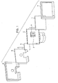
- Fig. 1 is an exploded perspective view of a liquid crystal display according to an embodiment of the present invention.
- Fig. 2 is an exploded perspective view of the liquid crystal module and photodetector of Fig. 1.
- Fig. 3 is a schematic block diagram of a control circuit which detects light from a backlight with a light sensor, shown in Figs. 1 and 2, to control the quantity of light.
- Fig. 4 is a flow chart for describing a specific operation of an embodiment of the present invention.
- Fig. 5 shows luminance variation characteristics of a cold cathode fluorescent tube employed in an embodiment of the present invention.
- a base 2 is provided at the rear of a liquid crystal module 1.
- a light sensor attached to a printed circuit board (PCB) 3 is fixed to a center location of base 2.
- the light sensor detects light from the backlight leaking out from the rear of liquid crystal module 1.
- a doughnut-shaped cushion 4 for blocking light is provided between liquid crystal module 1 and sensor PCB 3 so that the light sensor detects only the light from the backlight.
- a printed circuit board (PCB) 5 of a controller is provided at the rear of base 2.
- An aluminum blocking plate 6 is provided at the rear of PCB 5.
- Liquid crystal module 1, base 2, sensor PCB 3, doughnut-shaped cushion 4, PCB 5, and blocking plate 6 are formed integrally by a front cover 7 and a back cover 8. Although cushion 4 closely adheres to liquid crystal module 1 in order to block light, the pressure is such that no display unevenness will occur on LCD panel 11 due to the cushion effect.
- Fig. 2 is an exploded perspective view of the liquid crystal module and the photodetector shown in Fig. 1.
- liquid crystal module 1 includes an LCD panel 11, a diffusion sheet 12, a light collective sheet 13, a fluorescent tube 14, a light directing plate 15, and a reflector sheet 16.
- Fluorescent tube 14 is provided at both ends of light directing plate 15. The light from fluorescent tube 14 is directed onto LCD panel 11 by light directing plate 15, and the entire surface of LCD panel 11 is illuminated by light collective sheet 13 and diffusion sheet 12.
- Reflector sheet 16 is provided at the rear of light directing plate 15. Most of the light directed from light directing plate 15 is guided towards light collective sheet 13. However, a portion of light leaks from reflector sheet 16. This leakage light is detected by light sensor 10 attached to sensor PCB 3 via cushion 4. Sensor PCB 3 is attached to base 2 of Fig. 1 by a PCB attachment 9.
- a sense antenna 20 is provided around light sensor 10 on sensor PCB 3.
- Sense antenna 20 detects the electric field component leaking out from liquid crystal module 1. Unnecessary electric field radiation can be canceled for example, by applying an opposite polarity voltage of the detected electric field to an antenna (not shown) provided around liquid crystal module 1. The number of components can be reduced by attaching light sensor 10 and sense antenna 20 to sensor PCB 3. As a result, the cost can be reduced.
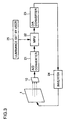
- Fig. 3 is a block diagram of a control circuit for controlling the luminance of the backlight.
- the detected output from light sensor 10 is provided to an A/D converter 21 to be converted into a digital signal.
- the digital signal is provided to a MPU 22.
- MPU 22 computes a luminance control signal so that fluorescent tube 14 emits light at the luminance level set by a user with a setting device 25.
- the output luminance control signal is converted into an analog signal by a D/A converter 23 to be provided to an inverter 24.
- Inverter 24 drives fluorescent tube 14 of liquid crystal module 1 according to the provided analog signal.
- the optimum display state can be maintained by MPU 22 providing a luminance control signal that attains the luminance set by the user through setting device 25 while monitoring the detected output of light sensor 10.
- light sensor 10 provided at the rear of liquid crystal module 1 detects light leaking from fluorescent tube 14 serving as a backlight. Therefore, a photodetector can be easily attached to a liquid crystal display including LCD panel 11, the backlight, light directing plate 15, reflector sheet 16 and the like, which are formed integrally. Accordingly, the cost can be reduced.
- Fig. 4 is a flow chart for describing the operation of a luminance control device according to another embodiment of the present invention.
- Fig. 5 shows the luminance variation characteristics of a cold cathode fluorescent tube.
- MPU 22 sets the maximum luminance of the backlight.
- This maximum luminance setting is implemented at the time of shipment, at the time of exchanging fluorescent tube 14 of Fig. 2, or at the time of exchanging light sensor 10.
- This setting is effected to absorb the difference in luminance for each set caused by variation in fluorescent tube 14 and by the sensitivity variation of light sensor 10. More specifically, fluorescent tube 14 is made to emit light at the maximum luminance of 100% and aged.
- MPU 22 stores the output of light sensor 10 that is converted into a digital signal by A/D converter 21. The stored value is the maximum luminance value (Ymax) of the set.
- MPU 22 controls the luminance of the backlight. This luminance control is repeated periodically in the general usage state after the above-described maximum luminance is set. More specifically, at step SP2, MPU 22 reads out the output of light sensor 10 that is converted into a digital signal by A/D converter 21. This is the current backlight luminance value (Y).
- the user luminance set value (UY) is read.
- This luminance set value (UY) can be set arbitrarily by a user by operation of a switch that is attached to the set. This value represents the desired usage in % with respect to the maximum luminance.
- MPU 22 computes the target luminance sensor value (YX) according to the maximum luminance Ymax and the user luminance set value (UY).
- step SP5 the luminance sensor value Y is compared with the target sensor value YX. When the compared values match, the process ends. Otherwise, control proceeds to step SP6. A predetermined value is added to (or subtracted from) the luminance control output value so that the luminance sensor value (Y) detected by light sensor 10 approximates the target luminance sensor value (YX).
- the computed luminance control output value is provided to D/A converter 23 at step SP7.
- the luminance control output value is converted into an analog signal by D/A converter 23. Therefore, when the luminance set value is set as 50%, for example, the backlight can emit substantially constant quantity of light even when the environmental conditions such as ambient temperature differ, as shown in Fig. 5.
- the screen luminance that varies set by set can be provided effectively 100%.
- Luminance control can be provided regardless of variation in the sensitivity of the light sensor 10.
- a stable light adjusted ratio (the ratio of the maximum luminance to the minimum luminance) can be ensured. It is also possible to identify the decreasing rate of the luminance due to degradation of fluorescent tube 14 by storing the initial maximum luminance. This value can be used as a reference for the time to exchange fluorescent tube 14.
- the quantity of light when the backlight is lit at the maximum luminance is detected and the backlight is controlled using the detected quantity of light as a reference, so that the luminance set by the user can be obtained.
- the effect of variations in the luminance of the backlight and in the sensitivity of the sensor itself can be canceled to provide accurate luminance.
Abstract
Description
Claims (11)
- A photodetector for detecting light from a backlight of a liquid crystal display, comprising a light sensor (10) provided at the rear of said liquid crystal display for detecting light leaking from said backlight.
- The photodetector of a liquid crystal display according to claim 1, wherein said liquid crystal display includes a liquid crystal panel (11), a diffusion sheet (12), a light collective sheet (13), a light directing plate (15), and a reflector sheet (16), which are arranged as a unit element,
wherein a fluorescent tube (14) for backlight is provided at an end of said light directing plate, and
wherein said light sensor (10) is provided at said reflector sheet side to detect light leaking from said reflector sheet. - The photodetector of a liquid crystal display according to claim 2, further comprising a cushion member (4) for directing only the light leaking from said reflector sheet to said light sensor.
- The photodetector of a liquid crystal display according to claim 3, wherein said light sensor is attached to a printed circuit board, and wherein a sense antenna (20) is provided around said light sensor for detecting electric field radiation from said liquid crystal display.
- A luminance control device for controlling luminance of a backlight (14) for illuminating a liquid crystal display (1), said luminance control device comprising:a photodetector (10) for detecting a quantity of light when said backlight is lit at a maximum luminance,luminance setting means (25) for setting a desired luminance by a user, andcontrol means (22) for controlling luminance of said backlight using a detected output of said photodetector when said backlight is lit at the maximum luminance as a reference so that the luminance set by said luminance setting means is achieved.
- The luminance control device of a liquid crystal display according to claim 5, wherein said liquid crystal display includes a liquid crystal panel (11), a diffusion sheet (12), a light collective sheet (13), a light directing plate (15) and a reflector sheet (16), which are arranged as a unit, wherein a fluorescent tube (14) for backlight is provided at an end of said light directing plate, and
wherein said light sensor (10) is provided at said reflector sheet side to detect light leaking from said reflector sheet. - The luminance control device of a liquid crystal display according to claim 6, further comprising a cushion member (4) for directing only the light leaking from said reflector sheet to said light sensor.
- The luminance control device of a liquid crystal display according to claim 7, wherein said photodetector is provided at the rear of said liquid crystal display.
- The luminance control device of a liquid crystal display according to claim 7, wherein said light sensor is attached to a printed circuit board, and wherein a sense antenna (20) is provided around said light sensor for detecting electric field radiation from said liquid crystal display.
- A method of controlling a luminance output by a backlight of a flat panel display, said method comprising;a) allowing a user to select a luminance setting, said setting being proportional to a predetermined constant luminance value for said backlight;b) measuring a luminance currently output by said backlight using a photodetector; andc) adjusting the luminance output by the backlight to equal said user-defined setting.
- A method according to claim 10, wherein said constant luminance value is a value previously measured for said backlight using said photodetector.
Applications Claiming Priority (6)
| Application Number | Priority Date | Filing Date | Title |
|---|---|---|---|
| JP2044297 | 1997-02-03 | ||
| JP20443/97 | 1997-02-03 | ||
| JP02044397A JP3171808B2 (en) | 1997-02-03 | 1997-02-03 | Liquid crystal display photodetector |
| JP02044297A JP3193315B2 (en) | 1997-02-03 | 1997-02-03 | Backlight brightness control device for liquid crystal display |
| JP2044397 | 1997-02-03 | ||
| JP20442/97 | 1997-02-03 |
Publications (3)
| Publication Number | Publication Date |
|---|---|
| EP0861017A2 true EP0861017A2 (en) | 1998-08-26 |
| EP0861017A3 EP0861017A3 (en) | 2001-11-21 |
| EP0861017B1 EP0861017B1 (en) | 2007-06-27 |
Family
ID=26357402
Family Applications (1)
| Application Number | Title | Priority Date | Filing Date |
|---|---|---|---|
| EP98300672A Expired - Lifetime EP0861017B1 (en) | 1997-02-03 | 1998-01-30 | Photodetector of liquid crystal display and luminance control therefor |
Country Status (3)
| Country | Link |
|---|---|
| US (1) | US6188380B1 (en) |
| EP (1) | EP0861017B1 (en) |
| DE (1) | DE69837976T2 (en) |
Cited By (10)
| Publication number | Priority date | Publication date | Assignee | Title |
|---|---|---|---|---|
| WO2000041378A1 (en) * | 1998-12-31 | 2000-07-13 | Nokia Mobile Phones Limited | Backlight for a portable device |
| WO2004104976A1 (en) * | 2003-05-22 | 2004-12-02 | Siemens Aktiengesellschaft | Arrangement comprising a panel pertaining to a flat screen |
| EP1713055A1 (en) * | 2003-11-19 | 2006-10-18 | Eizo Nanao Corporation | Luminance adjustment method, liquid crystal display device, and computer program |
| CN100369099C (en) * | 2002-11-12 | 2008-02-13 | 三星电子株式会社 | Liquid crystal display dvice and its driving method |
| CN100373442C (en) * | 2002-11-12 | 2008-03-05 | 三星电子株式会社 | Liquid crystal display and driving method thereof |
| US7492028B2 (en) | 2005-02-18 | 2009-02-17 | Semiconductor Energy Laboratory Co., Ltd. | Photoelectric conversion device and manufacturing method of the same, and a semiconductor device |
| US7772667B2 (en) | 2005-05-20 | 2010-08-10 | Semiconductor Energy Laboratory Co., Ltd. | Photoelectric conversion device and semiconductor device |
| CN102467884A (en) * | 2010-11-17 | 2012-05-23 | Lg电子株式会社 | Display device |
| US8610659B2 (en) | 2008-05-12 | 2013-12-17 | Blackberry Limited | Method and apparatus for automatic brightness adjustment on a display of a mobile electronic device |
| EP2960712A4 (en) * | 2013-02-25 | 2016-05-18 | Eizo Corp | Light sensor attachment structure of image display device |
Families Citing this family (35)
| Publication number | Priority date | Publication date | Assignee | Title |
|---|---|---|---|---|
| US6207842B1 (en) * | 1997-10-09 | 2001-03-27 | Mars Incorporated | Process for preparing procyanidin(4-6 or 4-8) oligomers and their derivatives |
| US6747638B2 (en) * | 2000-01-31 | 2004-06-08 | Semiconductor Energy Laboratory Co., Ltd. | Adhesion type area sensor and display device having adhesion type area sensor |
| TW518882B (en) * | 2000-03-27 | 2003-01-21 | Hitachi Ltd | Liquid crystal display device for displaying video data |
| US7030551B2 (en) | 2000-08-10 | 2006-04-18 | Semiconductor Energy Laboratory Co., Ltd. | Area sensor and display apparatus provided with an area sensor |
| JP2002072998A (en) * | 2000-08-25 | 2002-03-12 | Internatl Business Mach Corp <Ibm> | Luminance controller, luminance adjusting system, computer system, liquid crystal display device, luminance control method, computer program and storage medium |
| DE10057696A1 (en) * | 2000-11-21 | 2002-05-16 | Siemens Ag | LCD display with background lighting provided by a controlled light source |
| US6747290B2 (en) | 2000-12-12 | 2004-06-08 | Semiconductor Energy Laboratory Co., Ltd. | Information device |
| US6825828B2 (en) * | 2001-02-23 | 2004-11-30 | General Digital Corporation | Backlit LCD monitor |
| KR100392460B1 (en) * | 2001-05-21 | 2003-07-23 | 삼성전자주식회사 | Lcd monitor |
| US20030227435A1 (en) * | 2002-06-06 | 2003-12-11 | Chang-Fa Hsieh | Method for adjusting and detecting brightness of liquid crystal displays |
| US7609360B2 (en) * | 2002-06-17 | 2009-10-27 | Fujifilm Corporation | Image display device |
| US6734926B2 (en) * | 2002-09-13 | 2004-05-11 | Chi Mei Optoelectronics Corporation | Display apparatus with a reduced thickness |
| KR100712334B1 (en) * | 2002-09-30 | 2007-05-02 | 엘지전자 주식회사 | Method for controling a brightness level of LCD |
| JP3715616B2 (en) * | 2002-11-20 | 2005-11-09 | Necディスプレイソリューションズ株式会社 | Liquid crystal display device and common voltage setting method of the device |
| US20040233153A1 (en) * | 2003-05-22 | 2004-11-25 | Heber Robinson | Communication device with automatic display and lighting activation and method therefore |
| WO2005008320A1 (en) * | 2003-06-04 | 2005-01-27 | Seongju Lee | Inverter for eefl and backligth |
| CN100419534C (en) * | 2003-12-08 | 2008-09-17 | 索尼株式会社 | Liquid crystal display and backlight adjusting method |
| US7755593B2 (en) * | 2004-02-20 | 2010-07-13 | Sharp Kabushiki Kaisha | Display device, method of controlling same, computer program for controlling same, and computer program storage medium |
| US7342256B2 (en) * | 2004-07-16 | 2008-03-11 | Semiconductor Energy Laboratory Co., Ltd. | Display device mounted with read function and electric appliance |
| JP4550638B2 (en) * | 2005-03-22 | 2010-09-22 | シャープ株式会社 | Surface illumination device and liquid crystal display device including the same |
| KR100950518B1 (en) | 2005-07-18 | 2010-03-30 | 이노베이티브 솔루션즈 앤드 서포트 인코포레이티드 | Aircraft Flat Panel Display System |
| JP4633035B2 (en) | 2006-11-07 | 2011-02-16 | Necディスプレイソリューションズ株式会社 | Liquid crystal display device and liquid crystal display device control method |
| JP2008181109A (en) * | 2006-12-27 | 2008-08-07 | Semiconductor Energy Lab Co Ltd | Liquid crystal display device and electronic equipment using the same |
| US8514165B2 (en) * | 2006-12-28 | 2013-08-20 | Semiconductor Energy Laboratory Co., Ltd. | Semiconductor device |
| TW200840998A (en) * | 2007-04-14 | 2008-10-16 | Benq Corp | Display apparatus and brightness adjustment method thereof |
| KR20080101680A (en) | 2007-05-18 | 2008-11-21 | 가부시키가이샤 한도오따이 에네루기 켄큐쇼 | Liquid crystal display device, electronic device, and driving methods thereof |
| TW200907926A (en) * | 2007-08-06 | 2009-02-16 | Au Optronics Corp | Liquid crystal display and the backlight indicating apparathus and method thereof |
| TWI389091B (en) * | 2007-11-15 | 2013-03-11 | Young Lighting Technology Corp | Integrated driving board and liquid crystal display module having the same |
| US20090251400A1 (en) * | 2008-04-02 | 2009-10-08 | Hisense Beiging Electric Co., Ltd. | Lcd display method |
| JP4809453B2 (en) | 2009-04-15 | 2011-11-09 | 株式会社ナナオ | Display device, display system, and correction method |
| TWI547845B (en) * | 2009-07-02 | 2016-09-01 | 半導體能源研究所股份有限公司 | Touch panel and driving method thereof |
| JP5542409B2 (en) * | 2009-10-27 | 2014-07-09 | 三菱電機株式会社 | Multi-screen display device |
| JP2014232239A (en) * | 2013-05-30 | 2014-12-11 | Eizo株式会社 | Photosensor attachment structure of image display device |
| US9250692B2 (en) | 2013-09-10 | 2016-02-02 | Nvidia Corporation | Power-efficient personalization of a computing environment of a data processing device with respect to a user thereof |
| JP2015197607A (en) * | 2014-04-01 | 2015-11-09 | キヤノン株式会社 | Display device and control method of the same |
Citations (9)
| Publication number | Priority date | Publication date | Assignee | Title |
|---|---|---|---|---|
| JPS6026990A (en) * | 1983-07-25 | 1985-02-09 | キヤノン株式会社 | Display unit |
| US4760389A (en) * | 1985-11-27 | 1988-07-26 | Hosiden Electronics Co. Ltd. | Transmitting type display device |
| US5175637A (en) * | 1990-04-05 | 1992-12-29 | Raychem Corporation | Displays having improved contrast |
| JPH0513178A (en) * | 1991-07-02 | 1993-01-22 | Mitsubishi Electric Corp | Back-light for liquid crystal display device and liquid crystal display deivce |
| US5193201A (en) * | 1990-04-23 | 1993-03-09 | Tymes Laroy | System for converting a received modulated light into both power for the system and image data displayed by the system |
| JPH0611690A (en) * | 1992-06-26 | 1994-01-21 | Rohm Co Ltd | Liquid crystal display device |
| JPH06331962A (en) * | 1993-05-21 | 1994-12-02 | Keibunshiya:Kk | Liquid crystal display device |
| US5416385A (en) * | 1993-09-02 | 1995-05-16 | Rockwell International Corp. | Means for compact spatial optical integration |
| WO1995020180A1 (en) * | 1994-01-25 | 1995-07-27 | Fergason James L | Display system and method |
Family Cites Families (6)
| Publication number | Priority date | Publication date | Assignee | Title |
|---|---|---|---|---|
| JPH05127602A (en) | 1991-11-06 | 1993-05-25 | Matsushita Electric Ind Co Ltd | Illuminator |
| JPH05241512A (en) | 1992-02-28 | 1993-09-21 | Matsushita Electric Works Ltd | Display device |
| US5796451A (en) * | 1993-10-23 | 1998-08-18 | Samsung Display Devices Co., Ltd. | Liquid crystal cell with an external color filter |
| JP2830972B2 (en) * | 1995-03-06 | 1998-12-02 | 株式会社日立製作所 | Liquid crystal display |
| US5818553A (en) * | 1995-04-10 | 1998-10-06 | Norand Corporation | Contrast control for a backlit LCD |
| US5786801A (en) * | 1996-09-06 | 1998-07-28 | Sony Corporation | Back light control apparatus and method for a flat display system |
-
1998
- 1998-01-29 US US09/015,719 patent/US6188380B1/en not_active Expired - Lifetime
- 1998-01-30 DE DE69837976T patent/DE69837976T2/en not_active Expired - Lifetime
- 1998-01-30 EP EP98300672A patent/EP0861017B1/en not_active Expired - Lifetime
Patent Citations (9)
| Publication number | Priority date | Publication date | Assignee | Title |
|---|---|---|---|---|
| JPS6026990A (en) * | 1983-07-25 | 1985-02-09 | キヤノン株式会社 | Display unit |
| US4760389A (en) * | 1985-11-27 | 1988-07-26 | Hosiden Electronics Co. Ltd. | Transmitting type display device |
| US5175637A (en) * | 1990-04-05 | 1992-12-29 | Raychem Corporation | Displays having improved contrast |
| US5193201A (en) * | 1990-04-23 | 1993-03-09 | Tymes Laroy | System for converting a received modulated light into both power for the system and image data displayed by the system |
| JPH0513178A (en) * | 1991-07-02 | 1993-01-22 | Mitsubishi Electric Corp | Back-light for liquid crystal display device and liquid crystal display deivce |
| JPH0611690A (en) * | 1992-06-26 | 1994-01-21 | Rohm Co Ltd | Liquid crystal display device |
| JPH06331962A (en) * | 1993-05-21 | 1994-12-02 | Keibunshiya:Kk | Liquid crystal display device |
| US5416385A (en) * | 1993-09-02 | 1995-05-16 | Rockwell International Corp. | Means for compact spatial optical integration |
| WO1995020180A1 (en) * | 1994-01-25 | 1995-07-27 | Fergason James L | Display system and method |
Non-Patent Citations (3)
| Title |
|---|
| PATENT ABSTRACTS OF JAPAN vol. 017, no. 272 (E-1371), 26 May 1993 (1993-05-26) -& JP 05 013178 A (MITSUBISHI ELECTRIC CORP), 22 January 1993 (1993-01-22) * |
| PATENT ABSTRACTS OF JAPAN vol. 018, no. 211 (P-1726), 14 April 1994 (1994-04-14) -& JP 06 011690 A (ROHM CO LTD), 21 January 1994 (1994-01-21) * |
| PATENT ABSTRACTS OF JAPAN vol. 1995, no. 03, 28 April 1995 (1995-04-28) -& JP 06 331962 A (KEIBUNSHIYA:KK), 2 December 1994 (1994-12-02) * |
Cited By (17)
| Publication number | Priority date | Publication date | Assignee | Title |
|---|---|---|---|---|
| WO2000041378A1 (en) * | 1998-12-31 | 2000-07-13 | Nokia Mobile Phones Limited | Backlight for a portable device |
| CN100369099C (en) * | 2002-11-12 | 2008-02-13 | 三星电子株式会社 | Liquid crystal display dvice and its driving method |
| CN100373442C (en) * | 2002-11-12 | 2008-03-05 | 三星电子株式会社 | Liquid crystal display and driving method thereof |
| US7796113B2 (en) | 2003-05-22 | 2010-09-14 | Eizo Gmbh | Arrangement having a flat screen panel illuminated with a back light that compensates for changes in luminance of the panel |
| WO2004104976A1 (en) * | 2003-05-22 | 2004-12-02 | Siemens Aktiengesellschaft | Arrangement comprising a panel pertaining to a flat screen |
| US7952555B2 (en) | 2003-11-19 | 2011-05-31 | Eizo Nanao Corporation | Luminance control method, liquid crystal display device and computer program |
| EP1713055A4 (en) * | 2003-11-19 | 2009-04-22 | Eizo Nanao Corp | Luminance adjustment method, liquid crystal display device, and computer program |
| EP1713055A1 (en) * | 2003-11-19 | 2006-10-18 | Eizo Nanao Corporation | Luminance adjustment method, liquid crystal display device, and computer program |
| US7492028B2 (en) | 2005-02-18 | 2009-02-17 | Semiconductor Energy Laboratory Co., Ltd. | Photoelectric conversion device and manufacturing method of the same, and a semiconductor device |
| US7936037B2 (en) | 2005-02-18 | 2011-05-03 | Semiconductor Energy Laboratory Co., Ltd. | Photoelectric conversion device and manufacturing method of the same, and a semiconductor device |
| US7772667B2 (en) | 2005-05-20 | 2010-08-10 | Semiconductor Energy Laboratory Co., Ltd. | Photoelectric conversion device and semiconductor device |
| US8138004B2 (en) | 2005-05-20 | 2012-03-20 | Semiconductor Energy Laboratory Co., Ltd. | Photoelectric conversion device, manufacturing method thereof and semiconductor device |
| US8207591B2 (en) | 2005-05-20 | 2012-06-26 | Semiconductor Energy Laboratory Co., Ltd. | Photoelectric conversion device |
| US8610659B2 (en) | 2008-05-12 | 2013-12-17 | Blackberry Limited | Method and apparatus for automatic brightness adjustment on a display of a mobile electronic device |
| CN102467884A (en) * | 2010-11-17 | 2012-05-23 | Lg电子株式会社 | Display device |
| US8982039B2 (en) | 2010-11-17 | 2015-03-17 | Lg Electronics Inc. | Display device having luminance detecting optical sensor |
| EP2960712A4 (en) * | 2013-02-25 | 2016-05-18 | Eizo Corp | Light sensor attachment structure of image display device |
Also Published As
| Publication number | Publication date |
|---|---|
| US6188380B1 (en) | 2001-02-13 |
| EP0861017B1 (en) | 2007-06-27 |
| DE69837976T2 (en) | 2008-02-28 |
| EP0861017A3 (en) | 2001-11-21 |
| DE69837976D1 (en) | 2007-08-09 |
Similar Documents
| Publication | Publication Date | Title |
|---|---|---|
| EP0861017B1 (en) | Photodetector of liquid crystal display and luminance control therefor | |
| US6255784B1 (en) | Photopic brightness controller for fluorescent backlights | |
| US7717601B2 (en) | Systems and methods for compensating brightness uniformity of backlit image displays | |
| US20100060172A1 (en) | Hollow Planar Illuminating Apparatus | |
| JP5367883B2 (en) | Illumination device and display device including the same | |
| US9074929B2 (en) | Image display apparatus having a light guide unit refracting incident light from a screen to a sensor | |
| KR20070017695A (en) | Display device and driving method thereof | |
| US20110001728A1 (en) | Pointing device and display device using the same | |
| JP3193315B2 (en) | Backlight brightness control device for liquid crystal display | |
| JP2007214053A (en) | Light source module, light source system, and liquid crystal display device | |
| US9113511B2 (en) | Ambient light calibration for energy efficiency in display systems | |
| JP2006323311A (en) | Display apparatus | |
| JP3171808B2 (en) | Liquid crystal display photodetector | |
| US20120019494A1 (en) | Alignment factor for ambient lighting calibration | |
| US20040075045A1 (en) | Display | |
| KR20100008845A (en) | Apparatus and method for controlling back-light brightness | |
| JP2012014060A (en) | Liquid crystal display device and method for controlling backlight of the liquid crystal display device | |
| JP2000294026A (en) | Backlight device | |
| JPH1020277A (en) | Liquid crystal display device | |
| US10255842B2 (en) | Displaying system having a function of sensing displaying properties | |
| JP2003078838A (en) | Optical sensor and display device provided with the same | |
| JP2010191286A (en) | Liquid crystal display | |
| JPH1195215A (en) | Liquid crystal display device | |
| JP4769969B2 (en) | Image display device | |
| JP3036474B2 (en) | Backlight device |
Legal Events
| Date | Code | Title | Description |
|---|---|---|---|
| PUAI | Public reference made under article 153(3) epc to a published international application that has entered the european phase |
Free format text: ORIGINAL CODE: 0009012 |
|
| AK | Designated contracting states |
Kind code of ref document: A2 Designated state(s): AT BE CH DE DK ES FI FR GB GR IE IT LI LU MC NL PT SE Kind code of ref document: A2 Designated state(s): CH DE FI FR GB IT LI NL SE |
|
| AX | Request for extension of the european patent |
Free format text: AL;LT;LV;MK;RO;SI |
|
| PUAL | Search report despatched |
Free format text: ORIGINAL CODE: 0009013 |
|
| AK | Designated contracting states |
Kind code of ref document: A3 Designated state(s): AT BE CH DE DK ES FI FR GB GR IE IT LI LU MC NL PT SE |
|
| AX | Request for extension of the european patent |
Free format text: AL;LT;LV;MK;RO;SI |
|
| RIC1 | Information provided on ipc code assigned before grant |
Free format text: 7H 05B 41/392 A, 7G 02F 1/1335 B |
|
| 17P | Request for examination filed |
Effective date: 20011212 |
|
| AKX | Designation fees paid |
Free format text: CH DE FI FR GB IT LI NL SE |
|
| 17Q | First examination report despatched |
Effective date: 20020812 |
|
| GRAP | Despatch of communication of intention to grant a patent |
Free format text: ORIGINAL CODE: EPIDOSNIGR1 |
|
| RTI1 | Title (correction) |
Free format text: PHOTODETECTOR OF LIQUID CRYSTAL DISPLAY AND LUMINANCE CONTROL THEREFOR |
|
| GRAS | Grant fee paid |
Free format text: ORIGINAL CODE: EPIDOSNIGR3 |
|
| GRAA | (expected) grant |
Free format text: ORIGINAL CODE: 0009210 |
|
| RAP1 | Party data changed (applicant data changed or rights of an application transferred) |
Owner name: EIZO NANAO CORPORATION |
|
| AK | Designated contracting states |
Kind code of ref document: B1 Designated state(s): CH DE FI FR GB IT LI NL SE |
|
| REG | Reference to a national code |
Ref country code: GB Ref legal event code: FG4D |
|
| REG | Reference to a national code |
Ref country code: CH Ref legal event code: EP |
|
| REF | Corresponds to: |
Ref document number: 69837976 Country of ref document: DE Date of ref document: 20070809 Kind code of ref document: P |
|
| REG | Reference to a national code |
Ref country code: CH Ref legal event code: NV Representative=s name: FREI PATENTANWALTSBUERO |
|
| REG | Reference to a national code |
Ref country code: SE Ref legal event code: TRGR |
|
| ET | Fr: translation filed | ||
| PLBE | No opposition filed within time limit |
Free format text: ORIGINAL CODE: 0009261 |
|
| STAA | Information on the status of an ep patent application or granted ep patent |
Free format text: STATUS: NO OPPOSITION FILED WITHIN TIME LIMIT |
|
| 26N | No opposition filed |
Effective date: 20080328 |
|
| PGFP | Annual fee paid to national office [announced via postgrant information from national office to epo] |
Ref country code: FI Payment date: 20100114 Year of fee payment: 13 |
|
| PG25 | Lapsed in a contracting state [announced via postgrant information from national office to epo] |
Ref country code: FI Free format text: LAPSE BECAUSE OF NON-PAYMENT OF DUE FEES Effective date: 20110130 |
|
| REG | Reference to a national code |
Ref country code: CH Ref legal event code: PFA Owner name: EIZO CORPORATION, JP Free format text: FORMER OWNER: EIZO NANAO CORPORATION, JP Ref country code: CH Ref legal event code: NV Representative=s name: P&TS SA, CH |
|
| REG | Reference to a national code |
Ref country code: NL Ref legal event code: TD Effective date: 20150807 Ref country code: DE Ref legal event code: R082 Ref document number: 69837976 Country of ref document: DE Representative=s name: ISARPATENT - PATENTANWAELTE- UND RECHTSANWAELT, DE Ref country code: DE Ref legal event code: R082 Ref document number: 69837976 Country of ref document: DE Representative=s name: ISARPATENT PATENTANWAELTE BEHNISCH, BARTH, CHA, DE Ref country code: DE Ref legal event code: R081 Ref document number: 69837976 Country of ref document: DE Owner name: EIZO CORPORATION, JP Free format text: FORMER OWNER: EIZO NANAO CORP., MATTO, ISHIKAWA, JP |
|
| REG | Reference to a national code |
Ref country code: FR Ref legal event code: CD Owner name: EIZO CORPORATION, JP Effective date: 20150917 Ref country code: FR Ref legal event code: CA Effective date: 20150917 |
|
| REG | Reference to a national code |
Ref country code: FR Ref legal event code: PLFP Year of fee payment: 19 |
|
| REG | Reference to a national code |
Ref country code: FR Ref legal event code: PLFP Year of fee payment: 20 |
|
| PGFP | Annual fee paid to national office [announced via postgrant information from national office to epo] |
Ref country code: NL Payment date: 20161212 Year of fee payment: 20 |
|
| PGFP | Annual fee paid to national office [announced via postgrant information from national office to epo] |
Ref country code: FR Payment date: 20161215 Year of fee payment: 20 |
|
| PGFP | Annual fee paid to national office [announced via postgrant information from national office to epo] |
Ref country code: SE Payment date: 20170111 Year of fee payment: 20 Ref country code: CH Payment date: 20170112 Year of fee payment: 20 Ref country code: DE Payment date: 20170125 Year of fee payment: 20 |
|
| PGFP | Annual fee paid to national office [announced via postgrant information from national office to epo] |
Ref country code: GB Payment date: 20170125 Year of fee payment: 20 |
|
| PGFP | Annual fee paid to national office [announced via postgrant information from national office to epo] |
Ref country code: IT Payment date: 20170123 Year of fee payment: 20 |
|
| REG | Reference to a national code |
Ref country code: DE Ref legal event code: R071 Ref document number: 69837976 Country of ref document: DE |
|
| REG | Reference to a national code |
Ref country code: NL Ref legal event code: MK Effective date: 20180129 |
|
| REG | Reference to a national code |
Ref country code: CH Ref legal event code: PL |
|
| REG | Reference to a national code |
Ref country code: GB Ref legal event code: PE20 Expiry date: 20180129 |
|
| REG | Reference to a national code |
Ref country code: SE Ref legal event code: EUG |
|
| PG25 | Lapsed in a contracting state [announced via postgrant information from national office to epo] |
Ref country code: GB Free format text: LAPSE BECAUSE OF EXPIRATION OF PROTECTION Effective date: 20180129 |