The present invention relates to electrostatic chucks useful for
holding substrates during processing.
Electrostatic chucks are used to hold semiconductor substrates,
such as silicon wafers, in a process chamber. A typical electrostatic chuck
comprises an electrode covered by a dielectric layer. In monopolar chucks,
an attractive electrostatic force is generated when the electrode of the chuck
is electrically biased by a voltage and an electrically charged plasma in the
chamber induces electrostatic charge in the substrate. A bipolar chuck
comprises bipolar electrodes that are electrically biased relative to one
another to generate the electrostatic attractive force.
The electrostatic attractive force generated by electrostatic
chucks can also be of different types. As schematically illustrated in Figure
1a, a chuck 10a having a dielectric layer 11 with a high electrical resistance
results in coulombic electrostatic forces where opposing electrostatic charges
accumulate in the substrate 12 and in the electrode 13 of the chuck. The
coulombic electrostatic force is described by the equation:
F = 12 ε0εr V t A
where ε0 and εr are the dielectric constant of vacuum and relative dielectric
constant of the dielectric layer 11, respectively, V is the voltage applied to
the electrode 13, A is the area of the electrode, and t is the thickness of the
dielectric layer.
With reference to Figure 1b, Johnsen-Rahbek electrostatic
attraction forces occur in the chuck 10b when an air-gap or interface 14
between a low resistance or leaky dielectric layer 15 and the substrate 12,
has an interfacial contact resistance much greater than the resistance of the
dielectric layer 15, i.e., when the resistance of the dielectric layer 15 is
typically from about 1011 to about 1014 Ω/cm. Free electrostatic charge drifts
through the dielectric layer 15 in the applied electric field, and accumulates
at the interface of the dielectric layer 15 and the substrate 12. The charge
accumulated at the interface generates a potential drop represented by the
equation:
F = 12 ε0 V δ A
where δ denotes the contact resistance of the interface 14 between the
substrate 12 and the low resistance dielectric layer 15. The Johnsen-Rahbek
electrostatic attractive force is typically higher than that provided by
coulombic forces, because polarization in the dielectric layer 15, and free
charges accumulated at the interface 14 combine to enhance electrostatic
force. This provides a stronger electrostatic force that more securely holds
the substrate 12 onto the chuck and also improves thermal transfer rates at
the interface. Also, the lower voltages used in these chucks reduce the
possibility of charge-up damage to active devices on the substrate 12.
The dielectric layers 11, 15 covering the electrode 13 of these
chucks typically comprise a thin polymer film, such as polyimide, adhered to
the electrode, as for example disclosed in U.S. Patent No. 08/381,786,
entitled "Electrostatic Chuck with Conformal Insulator Film," filed on January
31, 1995, to Shamouilian, et al., which is incorporated herein by reference.
However, the substrate held on the chuck often breaks or chips to form
fragments having sharp edges that puncture the polymer film and expose the
electrode. Exposure of the electrode at even a single pinhole in the dielectric
layer can cause arcing between the electrode and plasma, and require
replacement of the entire chuck. Polymers also have a limited lifetime in
erosive process environments, such as processes using oxygen-containing
gases and plasmas. Also, polymers or adhesives used to bond the polymer
films to the chuck often cannot operate at elevated temperatures exceeding
1000°C.
Polycrystalline ceramics have also been used to form the
dielectric layer to provide increased puncture resistance and higher
temperature performance, as for example, described in U.S. Patent No.
5,280,156 to Niori; U.S. Patent No. 4,480,284; Watanabe, et al., in
"Relationship between Electrical Resistivity and Electrostatic Force of
Alumina Electrostatic Chuck," Jpn. J. Appl. Phys., Vol. 32, Part 1, No. 2,
(1993); or "Resistivity and Microstructure of Alumina Ceramics Added with
TiO2 Fired in Reducing Atmosphere," J. of the Am. Cer. Soc. of Japan Intl.
Ed., Vol. 101, No. 10, pp. 1107-1114 (July 1993); all of which are
incorporated herein by reference. The ceramic dielectric layers typically
comprise a low conductivity polycrystalline ceramic, such as a mixture of
Al2O3 and TiO2, or BaTiO3. However, polycrystalline ceramics such as Al2O3
doped with TiO2 often have an electrical resistance that changes with
temperature, and can exhibit low or insufficient electrical resistance at high
temperatures. Also, polycrystalline ceramics comprise small grains or
crystals that typically have a diameter of 0.1 to 50 microns, and have grain
boundaries containing a mixture of glassy materials that hold the grains
together. When such ceramic layers are exposed to erosive environments,
such as a fluorine containing plasmas, the plasma etches away the grain
boundary regions causing the ceramic grains to loosen and flake off during
processing of the substrate. Abrasion of the substrate against the chuck can
also cause ceramic grains to flake off the chuck. These particulate ceramic
grains contaminate the substrate and/or process chamber and reduce the
yields of integrated circuit chips from the substrate.
Dielectric layers comprising a thin wafer of monocrystalline
ceramic that is made of a few, relatively large, ceramic crystals have also
been used to cover the electrode. For example, U.S. Patent Application No.
5,413,360 to Atari, et al., describes an electrostatic chuck consisting of a
monocrystalline ceramic wafer covering an electrode on a dielectric plate.
Atari teaches that a bonding agent, or a high temperature joining method, is
used to join the monocrystalline ceramic wafer to the electrode of the chuck.
In another example, U.S. Patent No. 5,535,090 to Sherman, filed March 3,
1994, discloses an electrostatic chuck comprising small segments of
monocrystalline ceramic wafers adhered to the surface of an electrode using
a high temperature vacuum braze with a suitable brazing alloy. For example,
a platinum layer can be sputtered onto the monocrystalline ceramic layer and
a platinum paste used to adhere the monocrystalline ceramic layer to the
metal electrode.
One problem with such chucks arises from their structure,
which typically comprises a single relatively thin monocrystalline ceramic
wafer bonded to the metal electrode with a layer of bonding material
therebetween, and supported by a metal or dielectric plate made from
another material. During the bonding process or during use of the chuck in
an erosive process environment, the thermal expansion mismatch between
the monocrystalline ceramic wafer and the electrode can result in failure of
the bond. Also, the bonding material is typically a metal based material that
thermally or chemically degrades during use of the chuck in reactive
processes, causing failure of the chuck and movement or misalignment of the
substrate during processing. The thin monocrystalline ceramic wafer and
electrode can also separate from the supporting dielectric or metal plate at
high temperatures due to stresses arising from the thermal expansion
coefficient mismatches. Another problem arises because grooves, channels,
and other hollow spaces which are used to hold coolant or to supply helium
gas to the interface below the substrate, are difficult to form in the brittle,
hard, and thin monocrystalline ceramic layers. During the series of
machining or drilling steps that are used to form these hollow shapes, the
brittle layers often crack or chip resulting in loss of the chuck. It is also
difficult to precisely machine fine holes or grooves in the monocrystalline
ceramic wafer.
Yet another problem with such conventional chucks arises from
the method of fabrication of the monocrystalline ceramic wafers. In one
method, the Czochralski-type method, large crystals of monocrystalline
ceramic are drawn from molten alumina using a seeding crystal mounted on a
die. The drawn out material cools and solidifies to form a column of large
and oriented crystals. Thereafter, the column is sliced to form
monocrystalline ceramic wafers. Another method commonly known as the
EFG process (edge-defined, film fed, growth process) is taught for example,
by U.S. Patent Nos. 3,701,636 and 3,915,662 to La Bella, et al., both of
which are incorporated herein by reference. In these methods, a single
crystal of monocrystalline ceramic is drawn from molten alumina, using a die
such as an annular ring contacting the molten alumina in a capillary tube.
The molten alumina rises in the tube via capillary forces and the die provides
a seeding surface from which the monocrystalline ceramic crystal is grown.
However, the size of the monocrystalline ceramic crystal grown by these
methods is restricted by the dimensions of the size of the die opening,
preventing growth of large monocrystalline ceramic crystals need for large
diameter chucks. The fabrication methods can also produce crystals having
relatively small grains and with facet defects. Also, the drawn out crystal
can twist and turn during the drawing out process to provide a disoriented
and faceted crystalline structure.
It is desirable to have a chuck made of monocrystalline ceramic
that exhibits reduced thermal expansion mismatch, low rates of erosion in
plasma environments, and reduced particulate generation during use in
semiconductor processing. It is also desirable for the monocrystalline
ceramic used in the chuck to provide stable and reliable electrical properties
at high operating temperatures, preferably exceeding about 1000°C. It is
further desirable to have predefined shapes of grooves, slots and channels
for holding cooling fluid or helium gas in the body of the chuck to regulate
the temperatures of the substrate and chuck.
An electrostatic chuck of the present invention comprises
monocrystalline ceramic material that exhibits reduced erosion, is resistant to
particle generation, and provides reliable and stable electrical properties at
high operating temperatures. The electrostatic chuck preferably comprises a
monocrystalline ceramic monolith having a receiving surface for receiving a
substrate. An electrode is embedded in the monocrystalline ceramic
monolith for generating an electrostatic force for electrostatically holding the
substrate. An electrical connector extending through the monolith is used to
supply a voltage to operate the electrode. Preferably, the monocrystalline
ceramic comprises large crystals having a diameter of about 0.5 to about
10 cm, which are substantially oriented to one another in a single
crystallographic direction. The electrode of the chuck comprises a pattern of
lattice defects induced in the ceramic plates, a pattern of dopant in the
ceramic plates, or an electrode made of conducting metal. The
monocrystalline ceramic chuck can be operated at elevated temperatures
with little or no contamination of the substrate.
Another preferred version of the electrostatic chuck comprises a
monocrystalline ceramic layer covering a mesh electrode on an underlying
dielectric layer. The monocrystalline ceramic comprises large crystals that
are substantially oriented to one another, and that have integral bonding
interconnects that extend through apertures in the mesh electrode to bond
directly to the underlying dielectric layer. Preferably, the monocrystalline
ceramic layer is bonded directly to the underlying dielectric layer substantially
without any adhesive layer. More preferably, one or more of the
monocrystalline ceramic layer and underlying dielectric layer, are made from
single crystal of sapphire.
Yet another version of the electrostatic chuck, useful for
regulating the temperature of a substrate, comprises a dielectric member
having an electrode embedded therein and a receiving surface for receiving
the substrate. The dielectric member comprises a fluid conduit for circulating
heat transfer fluid in the chuck. Preferably, the fluid conduit comprises first
passageways at a distance D1 from the receiving surface, and second
passageways at a distance D2 from the receiving surface, the distance D1
being greater than the distance D2. Preferable, the first passageways are
adjacent to a fluid inlet that supplies heat transfer fluid to the conduit and the
second passageways are adjacent to a fluid outlet that removes the heat
transfer fluid. The distance D1 is sufficiently greater than the distance D2 to
compensate for a rise in temperature or cooling of the heat transfer fluid as it
circulates through the chuck. In one version, the fluid conduit comprises a
rectangular cross-section having a central axis that is at an angle to the
receiving surface. In another version, the fluid conduits comprise a helical
conduit rising toward the receiving surface from the fluid inlet to the fluid
outlet. In yet another version, circumferential inner and outer edges, the
inner edge being at a distance DIN from the receiving surface, and the outer
edge being at a distance DOT from the receiving surface, the difference
between the distance DIN and the distance DOT selected to maintain a
substantially uniform rate of thermal transfer across the receiving surface of
the chuck.
The electrostatic chuck can be fabricated by a variety of
methods, including bonding a plurality of monocrystalline ceramic plates to
one another to form a unitary monolithic structure, or directional solidification
of molten ceramic, or moving a capillary tube method to seed a
monocrystalline layer over an electrode. The first method uses a plurality of
monocrystalline ceramic plates, such as sapphire, and forms an electrode on
one or more of the monocrystalline ceramic plates. The monocrystalline
ceramic plates are bonded to one another to form a monolithic structure
having the electrode embedded therein. The monocrystalline ceramic plates
can be bonded to one another by applying a bonding compound comprising
aluminum oxide to the monocrystalline ceramic plates and heat treating the
bonding compound. Preferably, the bonding compound comprises an
eutectic mixture of aluminum oxide and eutectic component, the eutectic
mixture having an melting temperature of less than about 2000°C.
In another preferred method of forming the electrostatic chuck, ceramic
material is melted in a mold to form molten ceramic, the mold having an
internal shape of an electrostatic chuck. One or more of electrode forms,
channel forms, and conduit forms are held in the molten ceramic, and a
seeding crystal is maintained in contact with the molten ceramic. The
molten ceramic is directionally cooled to form monocrystalline ceramic
comprising large crystals substantially oriented to one another, and having
the electrode, channel forms, or conduit forms embedded therein. One or
more of the electrode, channel, or conduit shaping forms in the
monocrystalline ceramic are then suitably treated, for example, in an
oxidation heat treatment or wet chemical etching process, to form a
monocrystalline ceramic monolith having an electrode, and channels or
conduits for holding heat transfer fluid or gas, respectively. The method
provides an intermediate product comprising a unitary monolithic
monocrystalline ceramic having embedded therein one or more chemically
erodible forms that are shaped to form channels and conduits.
In another preferred method of forming the electrostatic chuck, a ceramic
material is melted in a melt reservoir to form a molten ceramic. A capillary
tube is positioned in the melt reservoir, the capillary tube comprising an inlet
in the molten ceramic of the melt reservoir, and an outlet adjacent to a
workpiece surface (such as a mesh electrode held on a dielectric layer). The
outlet comprises a leading edge having a seeding surface and a first height,
and a trailing edge having a second height smaller than the first height. The
outlet of the capillary tube is moved across the workpiece surface so that the
leading edge of the capillary tube moves ahead of the trailing edge, to
deposit a molten ceramic layer on the workpiece surface. The molten
ceramic material is drawn through the capillary tube and seeded by a seeding
crystal on the seeding surface of the leading edge. The molten ceramic layer
has a thickness, t, substantially controlled by the difference in first and
second heights. Upon cooling, the seeded molten ceramic layer forms a
monocrystalline ceramic layer comprising large crystals substantially oriented
to one another. Preferably, the capillary tube and the workpiece surface are
continuously heated during deposition of the monocrystalline ceramic layer.
These features, aspects, and advantages of the present
invention will become better understood with regard to the following
description, appended claims, and accompanying drawings which illustrate
examples of the invention, where:
The present invention relates to an electrostatic chuck 20
comprising a unitary structure of a monocrystalline ceramic monolith 25
which comprises relatively large ceramic crystals 30 that are oriented to one
another in a single crystallographic direction, as schematically represented in
Figure 2a. The electrostatic chuck 20 of monocrystalline ceramic material
comprises a receiving surface 35 for receiving a substrate 40, and one or
more electrodes 45 embedded therein and below the receiving surface. As
shown in Figure 2a, the electrostatic chuck 20 electrostatically holds the
substrate 40 to the receiving surface 35 upon application of a voltage to the
electrode 45 via an electrical connector 50 that extends through the
monolithic structure 25.
The monocrystalline ceramic monolith 25 provides a unitary
block of a chemically homogeneous composition that has several advantages
in integrated circuit fabrication. The term "monocrystalline" which
commonly refers to a single crystal material, is used here to denotes material
that comprises a few (typically 10 or fewer) large ceramic crystals 30 that
are oriented in the same crystallographic direction, i.e., that have
crystallographic planes with miller indices that are aligned to one another.
The large crystals 30 of the monocrystalline ceramic typically have an
average diameter of about 0.5 to about 10 cm, and more typically from 1 to
5 cm. In contrast, conventional polycrystalline ceramic materials have small
grains or crystals with diameters on the order of 0.1 micron to 50 micron,
which is smaller by a factor of at least about 105 to about 107. The large
ceramic crystals 30 in the monolithic structure 25 are oriented in
substantially the same single crystallographic direction, and provide exposed
surfaces having little or no impurity or glassy grain boundary regions that can
erode rapidly in erosive halogen-containing environments as in small grains
and crystals. The continuously homogeneous and uniform crystallographic
structure of the receiving surface 35 of the monolith 25 exhibits reduced
erosion or particulate generation in erosive environments and provides a
relatively constant electrical resistance that does not change at higher
temperatures, unlike the receiving surfaces of polycrystalline ceramic chucks.
The highly oriented crystals of the monocrystalline ceramic
monolith 25 have a resistivity sufficiently high to electrically insulate the
electrode 45. The resistivity of the monolith 25 is preferably from about
1 x 10⁸ to about 1 x l020 Ω/cm, and more preferably from about 1 x 10¹¹ to
about 1 x 10¹³ Ω/cm; and is tailored to provide a resistance suitable for
forming either a coulombic electrostatic chuck (high resistance) or Johnsen-Rahbek
electrostatic chuck (low resistance). The monolith 25 reduces
particle generation during processing, provides excellent erosion resistance in
erosive halogen-containing plasma environments, and exhibits consistent
electrical resistance values at high temperatures, due to the presence of the
large ceramic crystals. Suitable monocrystalline ceramic materials include
monocrystalline Al2O3, AIN, BaTiO3, BeO, BN, CaO, LaB6, MgO, MoSi2, Si3N4,
SiO2, Ta2O5, TiB2, TiN, TiO2, TiSi2 VB2, W2B3, WSi2, ZrB2, or ZrO2.
Preferably, the ceramic monolith 25 comprises monocrystalline sapphire
which is a single crystal form of alumina that exhibits excellent chemical and
erosion resistance in erosive environments, particularly halogen plasma
environments. Monocrystalline sapphire also has a very high melting
temperature that allows high temperature use at temperatures exceeding
1000°C and often even exceeding 2000°C. The ceramic monolith 25 can
also be mixed with suitable dopants to provide the desired electrical
properties such as resistivity and dielectric breakdown strength. For
example, whereas pure sapphire has a resistivity on the order of 1 x 10¹⁴
Ω/cm, sapphire can be mixed with 1 to 3 wt% TiO2 to provide a lower
resistivity on the order of 1 x 10¹¹ to 1 x 10¹³ Ω/cm, which is more suitable
for use in Johnsen-Rahbek-type electrostatic chucks.
The electrode 45 of the electrostatic chuck 20 comprises one
of a pattern of dopant material, a pattern of lattice defects, or a metal
structure embedded in the ceramic monolith 25. Suitable metal electrodes
45 can be made from copper, nickel, chromium, aluminum, molybdenum, and
combinations thereof. In a preferred version, the electrode 45 comprises a
refractory metal having a melting point of at least about 2200°C to facilitate
fabrication of the electrostatic chuck 20, the thickness of the electrode being
from about 1 µm to about 100 µm, and more typically from 1 µm to 50 µm.
For a substrate 40 having a diameter of 200 to 300 mm (6 to 8 inches), the
electrode 45 typically covers a total area of about 7,000 to about 70,000 sq.
mm. Preferably, the electrode 45 comprises small apertures that are sized
(i) sufficiently small to allow the electrode to generate a uniform electrostatic
field for holding the substrate 40 upon application of a voltage thereto, and
(ii) sufficiently large to allow the monocrystalline ceramic monolith 25 to
form a strong and cohesive structure joined by interconnects extending
through the apertures. Electrical connectors 50 that are used to electrically
connect the electrode 45 to a chucking voltage supply 55, comprise an
electrical lead 60 that extends through the ceramic monolith 25 and an
electrical contact 65 at the end of the lead. Typically, the length of the
electrical lead 60 is from about 10 mm to about 50 mm, and the width of the
electrical lead is from about 0.2 mm to about 10 mm.
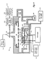
With reference to Figure 3, operation of the electrostatic chuck
20 of the present invention having a monopolar electrode 45 will be
described in the context of holding semiconductor substrates in a plasma
process chamber 70. The process chamber 70 illustrated in Figure 3
represents a CENTURA 5200 oxide etch chamber commercially available
from Applied Materials Inc., Santa Clara, California, as described in
commonly assigned U.S. Patent Application No. 07/941,507, filed on
September 8, 1992, which is incorporated herein by reference. The process
chamber 70 typically includes a process gas supply 75 for introducing
process gas into the process chamber via a gas distributor 80, and a
throttled exhaust 85 for exhausting gaseous byproducts from the process
chamber. A plasma is formed from the process gas using a plasma generator
that couples an electric field into the process chamber 70. The plasma
generator can comprise an inductor coil 90 capable of forming an inductive
electric field in the process chamber 70 when powered by a coil power
supply 95. Alternatively, the process chamber 70 can include process
electrodes 100, 105 that are used to generate a capacitive electric field in
the process chamber 70 when powered by a process electrode power supply
110. The process electrodes 100 can be the same electrode as the electrode
45 in the chuck 20 (not shown) or a separate electrode below the
electrostatic chuck as shown in Figure 3. The capacitive electric field formed
by the electrodes 100, 105 is perpendicular to the plane of the substrate 40
and accelerates inductively formed plasma species toward the substrate 40.
The frequency of the voltage applied to the process electrodes 100, 105,
and/or the inductor coil 90 is in the RF range, typically from about 50 kHz to
about 60 MHZ, and more typically about 13.56 MHZ. The power of the RF
voltage applied to the coil 90 or process electrodes 100, 105 is typically
from about 100 to about 5000 Watts. A combination of both inductor coils
90 and process electrodes 100, 105 is preferred to provide control of both
the plasma density and the plasma energy of the plasma ions.
In operation the process chamber 70 is evacuated and
maintained at a subatmospheric pressure and a robot arm (not shown)
transports a substrate 40 from a load-lock transfer chamber (also at
subatmospheric pressure) through a slit valve and into the process chamber
70. The robot arm places the substrate 40 on the tips of lift fingers (not
shown) that are elevated by the pneumatic lift mechanism to extend about 2
to 5 centimeters above the receiving surface 35 of the electrostatic chuck
20. The pneumatic mechanism lowers the substrate 40 onto the receiving
surface 35, and the electrode 45 of the electrostatic chuck 20 is electrically
biased with respect to the substrate by the chuck voltage supply 55. The
voltage applied to the monopolar electrode 45 shown in Figure 3 causes
electrostatic charge to accumulate in the electrode or in the monocrystalline
ceramic material covering the electrode. The plasma in the process chamber
70 provides electrically charged species having opposing polarity which
accumulate in the substrate 40. The accumulated opposing electrostatic
charges result in an attractive electrostatic force that electrostatically holds
the substrate 40 to the electrostatic chuck 20. On completion of processing,
the substrate 40 is electrically decoupled or dechucked from the electrostatic
chuck 20 by dissipating the residual electrical charges holding the substrate
onto the electrostatic chuck after the voltage to the electrode 45 is turned
off. The pneumatic lifting apparatus then raises the lift pins which lift the
substrate 40 to allow the substrate to be removed by the robotic arm.
Typically, the chucking voltage supply 55 is turned off, and the chucking
electrode 45 is connected to ground to remove any accumulated charge.
The substrate 40 can be electrically grounded by contacting it with a
grounded conductor or by forming a plasma at a reduced power level to
provide an electrically conductive path from the substrate to grounded walls
of the process chamber 70.
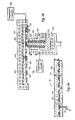
Another example of a process chamber 70 that can use the
present electrostatic chuck 20, as illustrated in Figure 4, comprises an RPS
process chamber, also commercially available from Applied Materials. In this
process chamber 70, the plasma is generated using a microwave generator
assembly 115 comprising a microwave applicator 120, a microwave tuning
assembly 125, and a magnetron microwave generator 130. A suitable
microwave applicator 120 comprises a microwave waveguide positioned in a
remote chamber in a flow path of the process gas as described in Applied
Materials U.S. Patent Application No. 08/499,984, by Herchen, et al.,
entitled "MICROWAVE PLASMA BASED APPLICATOR," filed on July 10,
1995, which is incorporated herein by reference. The electrostatic chuck 20
illustrated in this process chamber 70 comprises bipolar electrodes 45a, 45b
that includes at least two substantially coplanar electrodes that generate
substantially equivalent electrostatic clamping forces. The bipolar electrodes
45a, 45b can form opposing semicircles, or inner and outer rings of
electrodes with electrical isolation voids therebetween. The bipolar
electrodes 45a, 45b are operated by application of a differential electrical
potential to the electrodes that induces opposing electrostatic charges in the
substrate 40 to electrostatically hold the substrate to the electrostatic chuck
20.
In a preferred embodiment, a heat transfer gas supply 135
provides heat transfer gas to the receiving surface 35 of the electrostatic
chuck 20 to control the temperature of the substrate 40. In this version, the
ceramic monolith 25 comprises a gas channel 140 for holding heat transfer
gas in the electrostatic chuck 20, a gas feed 145 for providing heat transfer
gas to the gas channel, and gas vents 150 extending from the channel to the
receiving surface 35 for providing heat transfer gas to the receiving surface
35 below the substrate 40. During operation, the heat transfer gas flows
through the gas feed 145, into the gas channel 140, and out the gas vents
150, exiting below the receiving surface 35. The substrate 40 covers and
seals the gas vents 150 on the receiving surface 35 to reduce leakage of
heat transfer gas from below the substrate 40. The heat transfer gas
provides efficient heat transfer rates between the substrate 40 and the
electrostatic chuck 20 to maintain the substrate at constant temperatures.
Typically, the heat transfer gas is an inert gas such as helium or argon
supplied at a pressure of from about 5 to about 30 Torr.
In another aspect of the present invention, illustrated
schematically in Figure 4, a fluid system is used to regulate the temperature
of the electrostatic chuck 20 and the substrate 40. It should be noted that
the fluid system can be used in any support for holding the substrate 40, and
should not be limited to use in electrostatic chucks 20 comprising
monocrystalline ceramic material, which are used only to provide illustrative
examples of this aspect of the present invention. The fluid system comprises
(i) a fluid conduit 160 for holding or circulating heat transfer fluid below the
receiving surface 35 of the electrostatic chuck 20, (ii) a fluid inlet 165 for
supplying heat transfer fluid to the conduit 160, and (iii) a fluid outlet 170 for
removing or exhausting the heat transfer fluid from the electrostatic chuck
20. Preferably, the fluid conduit 160 is embedded in the electrostatic chuck
20 to provide more control over the temperature of the electrostatic chuck
20, particularly when the electrostatic chuck is made of ceramic material
having a low thermal conductance, such as aluminum oxide or sapphire.
During operation, a fluid supply 175 supplies cooled or heated fluid to the
fluid inlet 165 of the fluid conduit 160. The fluid is pumped into the fluid
inlet 165 circulates through the fluid conduit 160 to heat or cool the
electrostatic chuck 20 (depending on the difference in temperature between
the fluid and the electrostatic chuck), and flows out from the fluid outlet
170. By virtue of being inside the electrostatic chuck 20, the fluid conduit
160 provides lower temperature adjustment response times and higher heat
transfer rates than conventional fluid systems in which a fluid is used to
control the temperature of a separate metal base below the electrostatic
chuck, where there are more thermal impedances between the heat sink of
the base and the substrate.
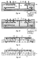
As illustrated in Figure 5a, preferably, the fluid conduit 160 in
the body of the electrostatic chuck 20 comprises first passageways 180 at a
first distance D1 from the receiving surface 35 and second passageways 185
at a second distance D2 from the receiving surface. The difference ΔD
between the distances D1 and D2 is selected to provide a uniform heat
transfer rate from the receiving surface 35 to the conduit 160, even though
the fluid is being heated or cooled by the electrostatic chuck 20 as it travels
through the electrostatic chuck. The distance D1 is sufficiently greater or
smaller than the distance D2 to compensate for the change in temperature of
the fluid as it flows through the electrostatic chuck 20. In other words, the
distance D1 is sufficiently greater or smaller than the distance D2 to
compensate for any difference in temperature ΔT of the fluid that would
otherwise cause dissimilar rates of heat transfer from different portions of
the receiving surface 35. In one embodiment, shown in Figure 5a, first
passageways 180 are positioned adjacent to the fluid inlet 165, while second
passageways 185 are positioned adjacent to the fluid outlet 170 closer to
the receiving surface 35. This arrangement compensates for the large
difference in temperature ΔT between the receiving surface 35 and the fluid
entering the body of the chuck 20 than the temperature difference between
the receiving surface 35 and fluid exiting the chuck 20. To maintain
substantially uniform temperatures at the receiving surface of the chuck 20,
the fluid inlet 165 is positioned further away from the receiving surface 35
than the fluid outlet 170. For example, one arrangement shown in Figure 5a
comprises a fluid conduit 160 that is shaped as a helical conduit that rises
toward the receiving surface 35 as it proceeds from the fluid inlet 165 to the
fluid outlet 170, with the distance D1 being sufficiently greater than the
distance D2 to provide uniform rates of thermal transfer across the receiving
surface 35.
The fluid conduit 160 with the first and second passageways
180, 185 provides more precise control of the temperature of the substrate
40 by compensating for variations in heat generation or heat conductance
across the electrostatic chuck 20, which is a particular problem for ceramic
chucks that contain different materials or internal structures, such as
electrodes, channels and conduits which have different thermal impedances.
The first and second passageways 180, 185 can comprise any suitable
structure for forming a continuous conduit 160 through the electrostatic
chuck 20, as apparent to one of ordinary skill in the art, that will provide the
desired differential or uniformity in temperatures across the receiving surface
35. For example, the fluid conduit 160 can include discrete segments having
polyhedra or rectangular shaped cross-sections below the receiving surface
35, segments that are positioned at an acute or obtuse angle relative to the
receiving surface, or a continuous conduit which ascends helically from a
perimetric portion to a central portion of the electrostatic chuck 20, or vice-versa.
In another embodiment of the chuck 20, the temperature profile
across the substrate 40 held on the receiving surface 35 is further controlled
by controlling the difference between the distance DIN which is the distance
between the receiving surface 35 and the radially inner portion of the fluid
conduit 160, and the distance DOT which is the distance between the
receiving surface 35 and the radially outer or perimetric portion of the fluid
conduit. The difference in the distances DIN and DOT is selected based on the
difference in equilibrium temperatures at the receiving surface 35, and can be
used to design a fluid conduit 160 in conjunction with the distances D1 and
D2, or independently. For example, Figure 5b shows a conduit where both
the distances DIN and DOT and the distances D1 and D2 were tailored to
achieve a uniform temperature across the receiving surface 35 and the
substrate 40. Figures 5c and 5e illustrate additional fluid conduits 160
comprising an outer circumferential diameter DOT at the perimeter of the
electrostatic chuck 20 that is closer to the receiving surface 35 than an inner
circumferential diameter DIN near the center of the electrostatic chuck. This
arrangement of the fluid conduit 160 provides increased heat transfer from
the peripheral portion of the electrostatic chuck 20, and is useful when the
peripheral portion operates at hotter steady state or equilibrium temperatures
than the central portion, so that the cooling fluid can cool the peripheral
portion at higher cooling rates than the center. Alternatively, when the
central portion of the electrostatic chuck 20 is hotter than the peripheral
portion, the fluid conduit 160 has the shape shown in Figure 5d, where the
inner circumferential diameter DIN near the center of the electrostatic chuck is
closer to the receiving surface 35 than the outer circumferential diameter
DOT, and the distance DIN is less than the distance DOT.
In one preferred embodiment, the fluid conduit 160 comprises
an annular ring that extends circumferentially through the electrostatic chuck
20 and has a rectangular cross-section with a central axis inclined to the
plane of the receiving surface 35, as shown in Figures 5b through 5d. The
angular orientation of the annular ring relative to the receiving surface 35 is
selected to maintain a substantially uniform temperature across the receiving
surface 35 from the perimeter to the center. The annular ring has an inner
circumferential edge at a distance DIN from the receiving surface 35, and an
outer circumferential edge at a distance DOT from the receiving surface 35.
In another version shown in Figure 5e, the fluid conduit 160 comprises one
or more passages having a circular cross-section that form an ascending
spiral about a central vertical axis of the electrostatic chuck 20. Other
equivalent fluid conduit structures and configurations, as apparent to one of
ordinary skill in the art, are also within the scope of the present invention.
One method of fabricating the electrostatic chuck 20 comprises
a melt forming and seeding process that produces a unitary structure of large
crystals 30 with an electrode 45 embedded therein. The melt process uses
an apparatus comprising a heated mold 200 for melting a ceramic material
for forming a molten ceramic, as shown in Figure 6a. The sidewalls of the
heated mold 200 are heated by a conventional heater 205, extending
through or wrapped around the mold. The mold 200 is preferably fabricated
from a material that uniformly wets the molten ceramic material, and,
because the molten ceramic should not be contaminated by dissolution of
mold material, is chemically stable with a high melting point. For fabricating
electrostatic chucks 20 composed of sapphire, the mold 200 is preferably
made of a material such as molybdenum, which has a melting point of
2617°C, uniformly wets molten alumina, and has a low reactivity and high
chemical compatibility with molten alumina. Cooling tubes (not shown)
containing a heat transfer fluid, such as water or helium gas, can also be
provided around the mold to provide a controlled source of heat dissipation.
One or more chemically degradable forms 210a-d which are
shaped to form the gas channel 140, gas feed 145, gas vents 150, and fluid
conduit 160 in the electrostatic chuck 20. The chemically degradable forms
210a-d and the electrode 45 or bipolar electrodes 45a, 45b of the
electrostatic chuck 20 are held suspended in the molten ceramic material by
fine alumina fibers or supported by alumina blocks.
During solidification of the molten ceramic in the mold 200, a
seeding crystal 215 is contacted against the surface of the molten ceramic to
seed or nucleate growth of a monocrystalline ceramic in the molten ceramic
material. The seeding crystal 215 typically comprises a crystal that has the
same composition as the molten ceramic material. Because the seeding
crystal 215 has an oriented crystallographic structure it serves as a seeding
or nucleating surface that initiates growth of a monocrystalline ceramic
structure. The surface of the molten ceramic is then slowly cooled while the
sidewalls and bottom of the mold 200 are continuously heated by the heater
205. This allows the molten ceramic to directionally solidify and grow
outwardly from the seeding crystal 215, to form a monocrystalline structure
that is conformal and confined to the internal shape of the mold 200. The
temperature of the mold 200 and the molten ceramic is controlled by a
temperature control system 220 that continuously heats the sidewalls and
bottom of the mold 200 while the molten ceramic is cooled from the surface
toward the bottom of the mold. Slowly reducing the heat applied to the
molten material allows the molten ceramic to form large, highly oriented
crystals 30.
After cooling, the solidified ceramic monolith 25 of
monocrystalline ceramic material is removed from the mold 200 and treated
to remove the chemically degradable forms 210a-d, creating conduits and
channels between the ceramic crystals 30 without damaging the electrostatic
chuck 20. The chemically degradable forms 210a-d are etched by a suitable
chemical, such as a bath of strong nitric acid, in which the ceramic monolith
25 is immersed for about 24 hours. Alternatively, chemically degradable
forms 210a-d can be made of a material, such as graphite, that is removed
through oxidation by simply heating the ceramic monolith 25 to a high
temperature of about 700°C in an atmosphere containing oxygen for about
120 minutes. When oxidation is used to remove the chemically degradable
forms 210a-d, care should be used to prevent unwanted oxidation of the
electrode 45. For example, when the electrode 45 is made from a refractory
metal, the electrode form should be flushed or purged with inert gas to
prevent oxidation and cracking of the electrode.
Several different methods can be used to form the electrode 45
in the electrostatic chuck 20. For example, as illustrated in Figures 6a to 6c,
a refractory metal electrode 210c,d is suspended in the molten ceramic to
become embedded in the monocrystalline monolith structure 25. Suitable
electrodes include, for example, an electrode formed from metal foil using
conventional bonding, stamping, or pressing methods; metal wire joined
together in an interconnected pattern to form a mesh of electrically
conductive wire; or a metal plate that is etched to form the desired electrode
pattern. Alternatively, the electrode can also be formed by altering the
crystalline lattice structure of the monocrystalline ceramic monolith 25 in a
predefined pattern to form a conductive electrode pattern on the crystal
structure. In this method, lattice defects are introduced in the
monocrystalline ceramic using a laser focused inside the ceramic monolith
25. Suitable laser methods can use a Nd YAG laser having an intensity of
108 Watts/cm2 that is scanned across the monocrystalline ceramic to form
electrically conducting lattice defects within the monocrystalline ceramic.
The lattice defects typically comprise dislocations, which occur when atoms
are moved from their initial crystalline positions to interstitial or other lattice
sites. In yet another method, the electrode 45 is formed by doping the
ceramic monolith 25 with suitable dopants to provide the desired electrical
properties such as resistivity and dielectric breakdown strength. For
example, a sapphire monocrystalline ceramic material can be doped with 0.1
to 5 wt% TiO2, in a conductive pattern suitable for use as an electrode 45.
Conventional photolithographic and ion implantation methods can also be
used to form a patterned layer of dopant on a sapphire layer.
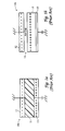
Another version of the electrostatic chuck 20 comprises a
plurality of monocrystalline ceramic plates 225 bonded to one another to
form the body of the electrostatic chuck, as shown in Figure 2b. The
electrode 45 is embedded in the electrostatic chuck 20, and the electrical
connector 50 extends through one or more monocrystalline ceramic plates
225 to supply a voltage to the electrode. Typically, the monocrystalline
ceramic plates 225 comprise a thickness of about 0.1 to 1 cms, and more
preferably 0.1 to 0.25 cms (0.04 to 0.10 inches) with a plurality of bonding
regions between the monocrystalline ceramic plates that typically have a
thickness of about .0001 to.0050 inches. The ceramic monolith 25
comprises from about 2 to about 30 monocrystalline ceramic plates 225.
One or more of the monocrystalline ceramic plates 225 have machined
therein (i) the gas channel 140, (ii) the gas feed 145, and (iii) gas vents 150
to provide heat transfer gas to the receiving surface 35 below the substrate
40. The monocrystalline ceramic plates 225 can also have machined therein
fluid conduit 160, fluid inlet 165, and fluid outlet 170. The monocrystalline
ceramic plates 225 are aligned to one another so that the gas channels 140,
gas feeds 145, and gas vents 150 form a continuos gas distribution path;
and the fluid conduit 160, fluid inlet 165, and fluid outlet 170 form a
separate continuos fluid path in the electrostatic chuck 20.
The method of fabricating an electrostatic chuck 20 which
comprises a plurality of monocrystalline ceramic plates 225, illustrated in
Figures 5a to 5c, will now be described. Conventional crystal growth
techniques, such as the Czochralski or EFG methods, in which a single
crystal of ceramic is seeded from molten ceramic, are used to grow a large
diameter single crystal of monocrystalline ceramic. The single crystal of
monocrystalline ceramic is cut into a number of monocrystalline ceramic
plates 225 comprising large aluminum oxide crystals 30 substantially
oriented with respect to one another. An electrode 45 comprising a metal
structure, a dopant pattern, or a pattern of lattice defects is formed on one
or more of the monocrystalline ceramic plates 225, as described above. The
monocrystalline ceramic plates 225 are bonded to one another to form a
ceramic monolith 25 using a eutectic bonding compound 230 comprising
mixture of aluminum oxide and a eutectic component. The bonding
compound 230 is selected to provide an aluminum oxide-containing bond
which matches the thermal expansion coefficient of the monocrystalline
ceramic plates 225, yet melts at a relatively low temperature. By eutectic
component it is meant an additive, or mixture of additives, that form an
eutectic or glassy system with aluminum oxide that has a melting
temperature that is significantly lower than that of pure aluminum oxide,
preferably less than about 2000°C, and more preferably less than about
1550°C. Preferred eutectic components include for example B2O3, P2O5, and
SiO2.
Several different methods can be used to form a metal
electrode 45 on one of the monocrystalline ceramic plates 225. In one
method, a patterned layer of resist is formed on one of the monocrystalline
ceramic plates 225, and metal deposited between the resist features (for
example, by electroplating or sputtering) to form an electrode 45 structure.
Suitable resist materials include "RISTON" fabricated by DuPont de Nemours
Chemical Co, and conventional photolithographic methods are described in
Silicon Processing for the VLSI Era, Volume 1: Process Technology, Chapters
12, 13, and 14, by Stanley Wolf and Richard N. Tauber, Lattice Press,
California (1986), which is incorporated herein by reference. Alternatively,
the electrode 45 can be fabricated by etching a layer of metal deposited on a
sapphire plate using conventional PVD, CVD, or solution deposition methods,
such as for example metal CVD or sputtering. Conventional
photolithographic and etching methods are used to etch the deposited metal
into the desired electrode configuration. The electrode 45 can also be
formed on a wafer of monocrystalline ceramic material cut from a column of
monocrystalline ceramic by altering the lattice structure of the ceramic wafer
in a predefined pattern to form a conductive electrode pattern, or by doping
the monocrystalline ceramic with suitable dopants to provide the desired
electrical properties such as resistivity and dielectric breakdown strength.
Yet another version of an electrostatic chuck 20 according to
the present invention, shown in Figure 8a, comprises a monocrystalline
ceramic layer 235 covering a mesh electrode 240 on an underlying dielectric
layer 245, the mesh electrode having predefined apertures 195 therethrough.
The underlying dielectric layer 245 can be formed from the same material as
the monocrystalline ceramic layer 235 or can be a different ceramic material.
The mesh electrode 240 is an electrically conductive patterned electrode.
Suitable materials for the monocrystalline ceramic layer and the underlying
dielectric layer 245 include Al2O3, BeO, SiO2, Ta2O5, ZrO2, CaO, MgO, TiO2,
BaTiO3, AIN, TiN, BN, Si3N4, ZrB2, TiB2, VB2, W2B3, LaB6, MoSi2, WSix, or
TiSix. Preferably, both the monocrystalline ceramic layer 235 and the
underlying dielectric layer 245 comprise sapphire. More preferably, the
thickness t of the monocrystalline ceramic layer 235 is at least about three
times the diameter of the apertures 195 between the patterned mesh
electrode 240 to reduce spreading of the electric field from the electrode.
Preferably, the monocrystalline ceramic layer 235 further
comprises integral bonding interconnects 190 that extend through the
apertures 195 in the mesh electrode 240 to form a unitary structure with the
underlying dielectric layer 245. The integral bonding interconnects 190
comprise posts of monocrystalline material having large oriented crystals 30
that bond directly to the underlying dielectric layer 245 substantially without
adhesive. The posts are formed when molten ceramic material is applied
over the exposed surface of the mesh electrode 240. The molten material
seeps into the apertures 195 of the mesh electrode 240 and fuses with the
underlying dielectric layer 245 to form a continuous and chemically bonded
ceramic structure enclosing the entire mesh electrode. Preferably, the
apertures 195 in the mesh electrode 240 are sized sufficiently small to allow
the mesh electrode to generate a uniform electrostatic field for holding the
substrate 40 upon application of a voltage thereto, and sufficiently large to
allow the integral bonding interconnects 190 formed therein to securely bond
the monocrystalline ceramic layer 235 to the underlying dielectric layer 245.
Elimination of the adhesive used to join conventional dielectric layers of
electrostatic chucks 20, through use of the integral bonding interconnects
190, provides more stable and reliable electrical properties at high operating
temperatures, exceeding about 1000°C, and often exceeding 2000°C.
Elimination of the adhesive also provides improved erosion resistance in
highly erosive plasma environments.
The method of fabricating the electrostatic chuck 20 of Figure
8a which comprises a monocrystalline ceramic layer 235, will now be
described. As shown in Figure 8b, the crystal growth apparatus comprises a
melt reservoir 250 for melting a ceramic material to form a molten ceramic.
The melt reservoir 250 is surrounded by ceramic fiber insulation 255, and
includes a conventional heater 205, such as tungsten or NICHROME wire,
wrapped around the melt reservoir. The melt reservoir 250 is typically made
of a corrosion resistant material capable of withstanding the high melting
temperatures of the ceramic material, such as molybdenum, which has a
melting point of 2617°C. Typical melting temperatures for such ceramic
materials often exceed 1000°C, for example, the melting or softening
temperature of alumina being 2015°C, of silicon dioxide being from 1200°C
to 1700°C, and of titanium dioxide being 1840°C.
A rigid capillary tube 260 is positioned in the molten ceramic of
the melt reservoir 250. The diameter of the capillary tube 260 is selected
based on the capillary surface tension forces of the particular ceramic
material melted in the reservoir 250. A typical diameter of the capillary tube
260 is from about 0.2 to about 2 mm. The rigid capillary tube 260 is self-filling
due to the capillary forces operating in the capillary tube that draws
molten ceramic material up the length of the capillary tube for feeding a
molten ceramic layer onto a workpiece surface 265, such as an exposed
surface of one or more mesh electrodes 240.
The capillary tube 260 comprises an inlet 270 immersed in the
molten ceramic in the reservoir, and an outlet 275 adjacent to the workpiece
surface 265, for example, the exposed surface of the electrode. The outlet
275 has (1) a leading edge 280 having a first height and a seeding surface
285, and (2) a trailing edge 290 having a second height smaller than the first
height. The thickness t of the monocrystalline ceramic layer 235 deposited
on the workpiece surface 265 is controlled by the difference in height of the
leading and trailing edges 280, 290 of the outlet 275, i.e., the difference in
first and second heights. The outlet 275 of the capillary tube 260 is moved
across the workpiece surface 265 in a direction such that leading edge 280
of the capillary tube 260 moves ahead of the trailing edge 290, to deposit on
the workpiece surface a layer of molten ceramic layer. The molten ceramic
layer is drawn through the capillary tube 260 by capillary forces and is
seeded by the seeding surface 285 of the leading edge 280 to form a
monocrystalline ceramic layer 235 on the workpiece surface 265.
The integral bonding interconnects 190 are formed during
deposition of the molten ceramic layer on the exposed surface of the
electrode of the electrostatic chuck 20, the molten ceramic material flows
thorough the apertures 195 in the mesh electrode 240 to bond directly to
junction regions on the underlying dielectric layer 245 that lying immediately
below the open apertures 195 of the mesh electrode. The resultant structure
eliminates the use of adhesives for bonding the underlying dielectric layer
245 below the electrode to the monocrystalline ceramic layer 235 covering
the electrode.
Preferably, the temperature of the capillary tube 260 and the
workpiece surface 265 is maintained uniform by a temperature control
system, which heats the capillary tube and workpiece surface during
deposition of the monocrystalline ceramic layer 235. Heating of the
workpiece surface 265 allows the coplanar ceramic layers to merge and flow
into one another to form a continuous ceramic layer covering the
substantially the entire workpiece surface. The temperature control system
comprises a heat shield, a heating and/or a cooling system, and a
temperature controller 300. The heat shield can comprise a cylinder of
ceramic fiber insulation 255 surrounding the capillary tube 260, and a box of
ceramic fiber insulation 295 surrounding the workpiece surface 265, suitable
ceramic insulation including ZIRCAR fibers, commercially available from
ZIRCAR Company. Preferably, the heat coil in the ceramic insulator is
connected to a closed loop temperature controller 300 to control the
temperature of the tube and workpiece surface 265. Cooling tubes 305 that
contain a heat transfer fluid, such as water or helium gas, can also be
provided around the capillary tube 260 and the workpiece surface 265 to
provide a source of rapid heat dissipation (not shown). The rate of growth of
the monocrystalline ceramic layer 235 is maximized by reducing heat loss
and minimizing thermal shocking of the deposited layer through use of the
temperature control system.
The capillary tube 260 is preferably fabricated from a material
that is chemically stable, has a high melting temperature, and uniformly wets
the molten ceramic material with a contact angle of less than about 90°. A
suitable high temperature material is molybdenum. Molybdenum also
uniformly wets molten alumina, and has a low reactivity and high chemical
compatibility with molten alumina.
The larger the height of the capillary tube 260, the less the
mechanical instabilities and perturbations formed in the molten ceramic layer
deposited on the workpiece surface 265. However, the maximum
permissible height of the capillary tube 260 depends on the surface tension
and density of the molten ceramic material in the capillary tube. Most
ceramic materials have a high surface tension, a low contact angle, and low
density, which provides relatively tall capillary rise. A suitable height of the
capillary tube 260 for molten alumina in a molybdenum capillary tube is at
least about 25 mm, and more preferably at least about 50 mm above the
melt surface in the melt reservoir 250.
The outlet 275 of the capillary tube 260 comprises a leading
edge 280 having a seeding surface 285. The seeding surface 285 seeds or
nucleates growth of a monocrystalline ceramic layer 235 from the molten
ceramic material. The seeding surface 285 typically comprises a seeding
crystal 215 of the same material as the monocrystalline ceramic material,
and serves as a seeding or nucleating surface that initiates growth of a
monocrystalline ceramic layer 235 on the workpiece surface 265.
The outlet 275 of the capillary tube 260 does not need to
match the shape of the area to be covered by the monocrystalline ceramic
layer 235, because the outlet deposits a ribbon of molten ceramic material on
the workpiece surface 265 as the outlet moves across the workpiece
surface. The workpiece surface 265 is continuously heated during
deposition of multiple ribbons of ceramic material, to a temperature close to
the melting temperature of the ceramic material deposited thereon, causing
the ribbons to flow into one another to form a ceramic layer that is
continuous and uniform across the workpiece surface 265. The width of
each ribbon of molten ceramic corresponds to the width w of the outlet 275,
and the height t of the ribbons corresponds to the difference in height of the
leading and trailing edges 280, 290, that define the outlet opening.
The capillary tube 260 and workpiece surface 265 are moved
relative to one another to deposit a uniform layer of molten ceramic material
on the electrode. Typically, the rate of movement of the molten ceramic
material through the capillary tube 260 is from about 10 to 100 cm/min; and
the rate of movement of the outlet 275 of the capillary tube is adjusted
accordingly to provide the desired thickness t of the monocrystalline ceramic
material on the workpiece surface 265. Preferably, the workpiece surface
265 is moved across the outlet 275 of the capillary tube 260 at a rate
sufficiently low to provide a melt interface that is mechanically stable. Since
the capillary tube 260 is fixed in the melt reservoir 250, the top of the
molten ceramic material in the tube and the crystal growth interface are both
relatively stationary with respect to the melt reservoir. Alternatively, the
outlet 275 of the capillary tube 260 along with the surrounding heat shield,
is moved across the workpiece surface 265. Multiple layers of
monocrystalline ceramic material, stacked onto top of one another, can be
deposited on the workpiece surface 265.
While the present invention has been described in considerable
detail with reference to certain preferred versions, many other versions
should be apparent to those of ordinary skill in the art. For example, the
monocrystalline ceramic can be fabricated by grain growth of polycrystalline
ceramic material or by other suitable melt forming methods. Also, the
electrode and other shapes can be formed by other methods, for example, by
drilling or machining a monocrystalline ceramic and inserting the desired
shapes and forms. Therefore, the scope of the appended claims
should not be limited to the description of the preferred versions contained
herein.