EP0863548B1 - Mounting assembly of integrated circuit device and method for production thereof - Google Patents
Mounting assembly of integrated circuit device and method for production thereof Download PDFInfo
- Publication number
- EP0863548B1 EP0863548B1 EP98103739A EP98103739A EP0863548B1 EP 0863548 B1 EP0863548 B1 EP 0863548B1 EP 98103739 A EP98103739 A EP 98103739A EP 98103739 A EP98103739 A EP 98103739A EP 0863548 B1 EP0863548 B1 EP 0863548B1
- Authority
- EP
- European Patent Office
- Prior art keywords
- integrated circuit
- circuit device
- holes
- mounting assembly
- substrate
- Prior art date
- Legal status (The legal status is an assumption and is not a legal conclusion. Google has not performed a legal analysis and makes no representation as to the accuracy of the status listed.)
- Expired - Lifetime
Links
Images
Classifications
-
- H—ELECTRICITY
- H01—ELECTRIC ELEMENTS
- H01L—SEMICONDUCTOR DEVICES NOT COVERED BY CLASS H10
- H01L24/00—Arrangements for connecting or disconnecting semiconductor or solid-state bodies; Methods or apparatus related thereto
- H01L24/80—Methods for connecting semiconductor or other solid state bodies using means for bonding being attached to, or being formed on, the surface to be connected
- H01L24/81—Methods for connecting semiconductor or other solid state bodies using means for bonding being attached to, or being formed on, the surface to be connected using a bump connector
-
- H—ELECTRICITY
- H01—ELECTRIC ELEMENTS
- H01L—SEMICONDUCTOR DEVICES NOT COVERED BY CLASS H10
- H01L23/00—Details of semiconductor or other solid state devices
- H01L23/48—Arrangements for conducting electric current to or from the solid state body in operation, e.g. leads, terminal arrangements ; Selection of materials therefor
- H01L23/488—Arrangements for conducting electric current to or from the solid state body in operation, e.g. leads, terminal arrangements ; Selection of materials therefor consisting of soldered or bonded constructions
- H01L23/498—Leads, i.e. metallisations or lead-frames on insulating substrates, e.g. chip carriers
- H01L23/49827—Via connections through the substrates, e.g. pins going through the substrate, coaxial cables
-
- H—ELECTRICITY
- H01—ELECTRIC ELEMENTS
- H01L—SEMICONDUCTOR DEVICES NOT COVERED BY CLASS H10
- H01L2224/00—Indexing scheme for arrangements for connecting or disconnecting semiconductor or solid-state bodies and methods related thereto as covered by H01L24/00
- H01L2224/01—Means for bonding being attached to, or being formed on, the surface to be connected, e.g. chip-to-package, die-attach, "first-level" interconnects; Manufacturing methods related thereto
- H01L2224/10—Bump connectors; Manufacturing methods related thereto
- H01L2224/12—Structure, shape, material or disposition of the bump connectors prior to the connecting process
- H01L2224/13—Structure, shape, material or disposition of the bump connectors prior to the connecting process of an individual bump connector
- H01L2224/13001—Core members of the bump connector
- H01L2224/13099—Material
- H01L2224/131—Material with a principal constituent of the material being a metal or a metalloid, e.g. boron [B], silicon [Si], germanium [Ge], arsenic [As], antimony [Sb], tellurium [Te] and polonium [Po], and alloys thereof
- H01L2224/13101—Material with a principal constituent of the material being a metal or a metalloid, e.g. boron [B], silicon [Si], germanium [Ge], arsenic [As], antimony [Sb], tellurium [Te] and polonium [Po], and alloys thereof the principal constituent melting at a temperature of less than 400°C
- H01L2224/13111—Tin [Sn] as principal constituent
-
- H—ELECTRICITY
- H01—ELECTRIC ELEMENTS
- H01L—SEMICONDUCTOR DEVICES NOT COVERED BY CLASS H10
- H01L2224/00—Indexing scheme for arrangements for connecting or disconnecting semiconductor or solid-state bodies and methods related thereto as covered by H01L24/00
- H01L2224/01—Means for bonding being attached to, or being formed on, the surface to be connected, e.g. chip-to-package, die-attach, "first-level" interconnects; Manufacturing methods related thereto
- H01L2224/10—Bump connectors; Manufacturing methods related thereto
- H01L2224/15—Structure, shape, material or disposition of the bump connectors after the connecting process
- H01L2224/16—Structure, shape, material or disposition of the bump connectors after the connecting process of an individual bump connector
- H01L2224/161—Disposition
- H01L2224/16151—Disposition the bump connector connecting between a semiconductor or solid-state body and an item not being a semiconductor or solid-state body, e.g. chip-to-substrate, chip-to-passive
- H01L2224/16221—Disposition the bump connector connecting between a semiconductor or solid-state body and an item not being a semiconductor or solid-state body, e.g. chip-to-substrate, chip-to-passive the body and the item being stacked
- H01L2224/16225—Disposition the bump connector connecting between a semiconductor or solid-state body and an item not being a semiconductor or solid-state body, e.g. chip-to-substrate, chip-to-passive the body and the item being stacked the item being non-metallic, e.g. insulating substrate with or without metallisation
- H01L2224/16237—Disposition the bump connector connecting between a semiconductor or solid-state body and an item not being a semiconductor or solid-state body, e.g. chip-to-substrate, chip-to-passive the body and the item being stacked the item being non-metallic, e.g. insulating substrate with or without metallisation the bump connector connecting to a bonding area disposed in a recess of the surface of the item
-
- H—ELECTRICITY
- H01—ELECTRIC ELEMENTS
- H01L—SEMICONDUCTOR DEVICES NOT COVERED BY CLASS H10
- H01L2224/00—Indexing scheme for arrangements for connecting or disconnecting semiconductor or solid-state bodies and methods related thereto as covered by H01L24/00
- H01L2224/80—Methods for connecting semiconductor or other solid state bodies using means for bonding being attached to, or being formed on, the surface to be connected
- H01L2224/81—Methods for connecting semiconductor or other solid state bodies using means for bonding being attached to, or being formed on, the surface to be connected using a bump connector
- H01L2224/818—Bonding techniques
- H01L2224/81801—Soldering or alloying
-
- H—ELECTRICITY
- H01—ELECTRIC ELEMENTS
- H01L—SEMICONDUCTOR DEVICES NOT COVERED BY CLASS H10
- H01L2924/00—Indexing scheme for arrangements or methods for connecting or disconnecting semiconductor or solid-state bodies as covered by H01L24/00
- H01L2924/01—Chemical elements
- H01L2924/01004—Beryllium [Be]
-
- H—ELECTRICITY
- H01—ELECTRIC ELEMENTS
- H01L—SEMICONDUCTOR DEVICES NOT COVERED BY CLASS H10
- H01L2924/00—Indexing scheme for arrangements or methods for connecting or disconnecting semiconductor or solid-state bodies as covered by H01L24/00
- H01L2924/01—Chemical elements
- H01L2924/01005—Boron [B]
-
- H—ELECTRICITY
- H01—ELECTRIC ELEMENTS
- H01L—SEMICONDUCTOR DEVICES NOT COVERED BY CLASS H10
- H01L2924/00—Indexing scheme for arrangements or methods for connecting or disconnecting semiconductor or solid-state bodies as covered by H01L24/00
- H01L2924/01—Chemical elements
- H01L2924/01006—Carbon [C]
-
- H—ELECTRICITY
- H01—ELECTRIC ELEMENTS
- H01L—SEMICONDUCTOR DEVICES NOT COVERED BY CLASS H10
- H01L2924/00—Indexing scheme for arrangements or methods for connecting or disconnecting semiconductor or solid-state bodies as covered by H01L24/00
- H01L2924/01—Chemical elements
- H01L2924/01029—Copper [Cu]
-
- H—ELECTRICITY
- H01—ELECTRIC ELEMENTS
- H01L—SEMICONDUCTOR DEVICES NOT COVERED BY CLASS H10
- H01L2924/00—Indexing scheme for arrangements or methods for connecting or disconnecting semiconductor or solid-state bodies as covered by H01L24/00
- H01L2924/01—Chemical elements
- H01L2924/01033—Arsenic [As]
-
- H—ELECTRICITY
- H01—ELECTRIC ELEMENTS
- H01L—SEMICONDUCTOR DEVICES NOT COVERED BY CLASS H10
- H01L2924/00—Indexing scheme for arrangements or methods for connecting or disconnecting semiconductor or solid-state bodies as covered by H01L24/00
- H01L2924/01—Chemical elements
- H01L2924/0105—Tin [Sn]
-
- H—ELECTRICITY
- H01—ELECTRIC ELEMENTS
- H01L—SEMICONDUCTOR DEVICES NOT COVERED BY CLASS H10
- H01L2924/00—Indexing scheme for arrangements or methods for connecting or disconnecting semiconductor or solid-state bodies as covered by H01L24/00
- H01L2924/01—Chemical elements
- H01L2924/01078—Platinum [Pt]
-
- H—ELECTRICITY
- H01—ELECTRIC ELEMENTS
- H01L—SEMICONDUCTOR DEVICES NOT COVERED BY CLASS H10
- H01L2924/00—Indexing scheme for arrangements or methods for connecting or disconnecting semiconductor or solid-state bodies as covered by H01L24/00
- H01L2924/01—Chemical elements
- H01L2924/01082—Lead [Pb]
-
- H—ELECTRICITY
- H01—ELECTRIC ELEMENTS
- H01L—SEMICONDUCTOR DEVICES NOT COVERED BY CLASS H10
- H01L2924/00—Indexing scheme for arrangements or methods for connecting or disconnecting semiconductor or solid-state bodies as covered by H01L24/00
- H01L2924/013—Alloys
- H01L2924/014—Solder alloys
-
- H—ELECTRICITY
- H01—ELECTRIC ELEMENTS
- H01L—SEMICONDUCTOR DEVICES NOT COVERED BY CLASS H10
- H01L2924/00—Indexing scheme for arrangements or methods for connecting or disconnecting semiconductor or solid-state bodies as covered by H01L24/00
- H01L2924/10—Details of semiconductor or other solid state devices to be connected
- H01L2924/11—Device type
- H01L2924/14—Integrated circuits
-
- H—ELECTRICITY
- H01—ELECTRIC ELEMENTS
- H01L—SEMICONDUCTOR DEVICES NOT COVERED BY CLASS H10
- H01L2924/00—Indexing scheme for arrangements or methods for connecting or disconnecting semiconductor or solid-state bodies as covered by H01L24/00
- H01L2924/15—Details of package parts other than the semiconductor or other solid state devices to be connected
- H01L2924/151—Die mounting substrate
- H01L2924/153—Connection portion
- H01L2924/1531—Connection portion the connection portion being formed only on the surface of the substrate opposite to the die mounting surface
- H01L2924/15311—Connection portion the connection portion being formed only on the surface of the substrate opposite to the die mounting surface being a ball array, e.g. BGA
Definitions
- the present invention relates to mounting assemblies of integrated circuit devices and methods for production thereof according to the respective preamble of claims 1 and 9, and more particularly, to a mounting assembly of an integrated circuit device in which an interconnection between an integrated circuit device and a mounting substrate is not exposed and also to a method for production thereof.
- a semiconductor chip assembly includes an integrated circuit device having a plurality of input/output terminals provided on the periphery of its top surface and a sheetlike interposer which is mounted on the integrated circuit device and has a plurality of bonding terminals provided on its periphery and connected to the plurality of input/output terminals of the integrated circuit device respectively.
- a sheetlike interposer Provided on the sheetlike interposer are a plurality of terminals for external connection which are connected to the plurality of bonding terminals through wires, respectively.
- the input/output terminals of the integrated circuit device and the plurality of bonding terminals of the sheetlike interposer are interconnected by respective bonding wires.
- the above prior art has such a problem that, since the input/output terminals of the integrated circuit device and the plurality of bonding terminals of the sheetlike interposer are interconnected by respective bonding wires, the bonding wires are externally exposed. This leads to another problem that the bonding tends to be easily separated, resulting in reduced reliability of package.
- One result of the present invention is to provide a mounting assembly of an integrated circuit device in which interconnections between a plurality of input/output terminals of the integrated circuit device and a plurality of connecting terminals of a wiring substrate on which the integrated circuit device is to be mounted can be carried out simultaneously.
- Yet another result of the present invention is to provide a mounting assembly of an integrated circuit device which can realize a firm interconnection between the integrated circuit device and a wiring substrate on which the integrated circuit device is to be mounted.
- a further result of the present invention is to provide a mounting assembly of an integrated circuit device in which interconnections between the integrated circuit device and a wiring substrate, on which the integrated circuit device is to be mounted, can be easily, visually observed.
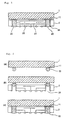
- FIG. 1 there is shown an embodiment of a mounting assembly of an integrated circuit device in accordance with the present invention, which includes an integrated circuit device 1 and a mounting substrate 2.
- the integrated circuit device 1 is provided on its bottom surface with a plurality of pads 11 for signal input/output or for power input.
- the pads 11 are arranged in rows along the periphery of the integrated circuit device 1.
- the pads 11 are made of copper or nickel.
- the mounting substrate 2 has therein wires 21, a plurality of through holes 22 and external terminals 23.
- the outside size of the mounting substrate 2 are made smaller than or equal to that of the integrated circuit device 1.
- the integrated circuit device 1 is mounted on the upper surface of the mounting substrate 2.
- the mounting substrate 2 comprises a laminate made up of a plurality of insulating layers and a plurality of wiring layers. By stacking these insulating layers and wiring layers, a desired arrangement of wires 21 is formed in the mounting substrate 2.
- the insulating layers are made of preferably material having thermal expansion coefficient of the same as or similar to that of the integrated circuit device 1. More specifically, the material of the insulating layers is ceramic, while the material of the wiring layers is copper.
- the through holes 22 each are disposed so as to be opposed to respective pads 11 provided on the integrated circuit device 1.
- the through holes 22 are formed so as to have a diameter of the same as or similar to that of the pads 11 of the integrated circuit device 1. More specifically the through holes 22 each have a diameter of 0.2 mm.
- a metallized electrode 24 is formed over the side surface of each of the through holes 22.
- the through holes 22 each are filled with solder 25.
- the electrodes 24 are connected to the wires 21 in the mounting substrate 2.
- Each of the electrodes 24, which is formed by plating the inside wall of the through holes 22 with copper, has a thickness of 1 micron.
- the external terminals 23 are arranged, on a lattice pattern, on the lower surface of the mounting substrate 2.
- the external terminals 23 are electrically connected respectively to the pads 11 of the integrated circuit device 1 through the wires 21, electrodes 24 and through-holes 22, respectively. That is, signals inputted from the external terminals 23 are transmitted to the integrated circuit device 1 through the wires 21, electrodes 24, solders 25 and pads 11 of the integrated circuit device 1.
- the solder 25 interconnects electrically and mechanically the electrodes 24 provided on the inside surface of the through hole 22 and the pad 11 of the integrated circuit device 1.
- the solder 25 is filled into the through holes 22 to such an extent that the solder can be visually checked from the lower side of the mounting substrate 2. More preferably, the solder is filled so as to be exposed from the lower surface of the mounting substrate 2, and the solder 25 is made of Sn/Pb alloy.
- the mounting substrate 2 to be mounted with the integrated circuit device 1 is provided with the through holes 22 at positions opposed to the pads 11 of the integrated circuit device 1 to connect the pads 11 to the through holes 22.
- the interconnection between the integrated circuit device 1 and the mounting substrate 2 is not exposed to the outside, with the result that the reliability of the connection can be improved.
- solder 25 filled into the through holes 22 can be observed from the lower side of the mounting substrate 2, and the connection between the pads 11 of the integrated circuit device 1 and the through holes 22 of the mounting substrate 2 can be checked.
- the fabricating method of the present invention is featured by a step of simultaneously interconnecting a plurality of pads 11 of the integrated circuit device 1 and through-holes 22 of the mounting substrate 2 by means of a connecting member.
- solder 25 is provided for each of the pads 11 provided on the lower surface of the integrated circuit device 1.
- the solder 25 is preferably comprised of a solder ball.
- the amount of each solder 25 is such that each through hole 22 of the mounting substrate 2 can be sufficiently filled with the solder.
- an alignment between the integrated circuit device 1 and the mounting substrate 2 is carried out. More in detail, the integrated circuit device 1 is positioned on the mounting substrate 2 so that the pads 11 on the lower side of the integrated circuit device 1 are opposed to the through holes 22 provided in the mounting substrate 2.
- both the integrated circuit device 1 and mounting substrate 2 are heated to melt the solders 25.
- the solders 25 are melted and filled into the through holes 22, so that the integrated circuit device 1 is electrically and mechanically connected to the mounting substrate 2.
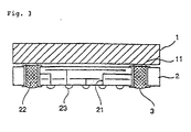
- the second embodiment of the present invention is featured in that the pads 11 provided on the lower side of the integrated circuit device 1 are electrically and mechanically connected to the through holes 22 of the mounting substrate 2 using electrically conductive resin.
- Other arrangement is substantially the same as that of the first embodiment.
- a conductive resin 3 is filled into each of through holes 22.
- the conductive resin 3 electrically connects the pad 11 of the integrated circuit device 1 and an electrode 24 provided on the inside wall of the through holes 22.
- the conductive resin 3 is for example epoxy resin. Employment of the conductive resin 3 restrains the amount of heat applied to the integrated circuit device 1 and mounting substrate 2 as compared with solder.
- the electrically conductive resin 3 is applied beforehand onto the pads 11 of the integrated circuit device 1.
- the conductive resin 3 is filled into the through holes 22 of the mounting substrate 2 beforehand.
- the integrated circuit device 1 and mounting substrate 2 are oppositely positioned so that the pads 11 of the mounting substrate 2 are aligned with through holes 22 filled with the conductive resin 3 respectively.
- the conductive resin 3 is such thermosetting resin as epoxy resin, when heated, the pads 11 are connected simultaneously to the through holes 22, respectively.
- the substrate may be made up of a single insulating layer and a single wiring layer provided thereon. In that case, a desired wiring is formed by the use of a single wiring layer.
- the insulating layers of the mounting substrate 2 are made of ceramic in the foregoing embodiments, the material of the insulating layers is not limited to the above example and the insulating layer may comprise such a flexible material as a polyimide film.
- a solder 25 exposed from the lower side of the mounting substrate 2 may be used as an electrode. Signals inputted from the electrodes 25 comprising exposed solder are transmitted to the pads 11 of the integrated circuit device 1 through the filled solder of the through holes 22.
- Such electrodes can be used more preferably as grounding electrodes, since the grounding electrodes have a width larger than that of the other wiring 21.
- the mounting assembly having the integrated circuit device mounted thereon is provided with the through-holes at such positions as to be opposed to the input/output terminals provided on the lower side of the integrated circuit device to connect the input/output terminals of the integrated circuit device with the through-holes, whereby the interconnection between the integrated circuit device and mounting substrate can be prevented from being outwardly exposed, thereby improving the interconnection reliability.
- connection between the input/output terminals of the integrated circuit device and the through-holes of the mounting substrate can be checked by observing the solder or conductive resin filled in the through-holes from the lower side of the mounting substrate.
- the integrated circuit device can be connected to the mounting substrate by heating the whole of the mounting substrate having the integrated circuit device mounted thereon to melt the solder or to thermally set the resin, the connections between input/output terminals of the integrated circuit device and through holes can be simultaneously effected.
Description
- The present invention relates to mounting assemblies of integrated circuit devices and methods for production thereof according to the respective preamble of
claims 1 and 9, and more particularly, to a mounting assembly of an integrated circuit device in which an interconnection between an integrated circuit device and a mounting substrate is not exposed and also to a method for production thereof. - An example of this type of prior art mounting assemblies of integrated circuit devices is disclosed in PCT International Publication Number 6-504408/94.
- In Fig. 13 of the above Publication, a semiconductor chip assembly includes an integrated circuit device having a plurality of input/output terminals provided on the periphery of its top surface and a sheetlike interposer which is mounted on the integrated circuit device and has a plurality of bonding terminals provided on its periphery and connected to the plurality of input/output terminals of the integrated circuit device respectively. Provided on the sheetlike interposer are a plurality of terminals for external connection which are connected to the plurality of bonding terminals through wires, respectively. The input/output terminals of the integrated circuit device and the plurality of bonding terminals of the sheetlike interposer are interconnected by respective bonding wires.
- The above prior art has such a problem that, since the input/output terminals of the integrated circuit device and the plurality of bonding terminals of the sheetlike interposer are interconnected by respective bonding wires, the bonding wires are externally exposed. This leads to another problem that the bonding tends to be easily separated, resulting in reduced reliability of package.
- In addition, since the bonding wires connecting the plurality of input/output terminals of the integrated circuit device and the plurality of bonding terminals of the sheetlike interposer are provided separately, a long manufacturing period of time is required.
- US 5 489 750 and EP 0 482 940 A1 disclose mounting assemblies of integrated circuit devices according to the preamble of
claim 1. - It is therefore the object of the present invention to provide a mounting assembly of an integrated circuit device which can avoid exposure of an interconnection between the integrated circuit device and a wiring substrate on which the integrated circuit device is to be mounted.
- The invention solves this object with the features of
claims 1 and 9. - One result of the present invention is to provide a mounting assembly of an integrated circuit device in which interconnections between a plurality of input/output terminals of the integrated circuit device and a plurality of connecting terminals of a wiring substrate on which the integrated circuit device is to be mounted can be carried out simultaneously.
- Yet another result of the present invention is to provide a mounting assembly of an integrated circuit device which can realize a firm interconnection between the integrated circuit device and a wiring substrate on which the integrated circuit device is to be mounted.
- A further result of the present invention is to provide a mounting assembly of an integrated circuit device in which interconnections between the integrated circuit device and a wiring substrate, on which the integrated circuit device is to be mounted, can be easily, visually observed.
- The above and other objects, features, and advantages of the present invention will become apparent from the following description referring to the accompanying drawings which illustrate an example of a preferred embodiment of the present invention.
-
- Fig. 1 is a cross-sectional view of a mounting assembly of an integrated circuit device in accordance with a first embodiment of the present invention;
- Fig. 2 shows a method for fabricating the mounting assembly of the embodiment; and
- Fig. 3 is a cross-sectional view of a mounting assembly of an integrated circuit device in accordance with the second embodiment of the present invention.
-
- A mounting assembly of an integrated circuit device and a method for production thereof in accordance with an embodiment of the present invention will be explained in detail with reference to the accompanying drawings.
- Referring first to Fig. 1, there is shown an embodiment of a mounting assembly of an integrated circuit device in accordance with the present invention, which includes an
integrated circuit device 1 and amounting substrate 2. - The
integrated circuit device 1 is provided on its bottom surface with a plurality ofpads 11 for signal input/output or for power input. Thepads 11 are arranged in rows along the periphery of theintegrated circuit device 1. Thepads 11 are made of copper or nickel. - The
mounting substrate 2 has thereinwires 21, a plurality of throughholes 22 andexternal terminals 23. The outside size of themounting substrate 2 are made smaller than or equal to that of theintegrated circuit device 1. Theintegrated circuit device 1 is mounted on the upper surface of themounting substrate 2. - The
mounting substrate 2 comprises a laminate made up of a plurality of insulating layers and a plurality of wiring layers. By stacking these insulating layers and wiring layers, a desired arrangement ofwires 21 is formed in themounting substrate 2. The insulating layers are made of preferably material having thermal expansion coefficient of the same as or similar to that of theintegrated circuit device 1. More specifically, the material of the insulating layers is ceramic, while the material of the wiring layers is copper. - The through
holes 22 each are disposed so as to be opposed torespective pads 11 provided on theintegrated circuit device 1. The throughholes 22 are formed so as to have a diameter of the same as or similar to that of thepads 11 of theintegrated circuit device 1. More specifically the throughholes 22 each have a diameter of 0.2 mm. Ametallized electrode 24 is formed over the side surface of each of the throughholes 22. The throughholes 22 each are filled withsolder 25. - The
electrodes 24 are connected to thewires 21 in themounting substrate 2. Each of theelectrodes 24, which is formed by plating the inside wall of the throughholes 22 with copper, has a thickness of 1 micron. - The
external terminals 23 are arranged, on a lattice pattern, on the lower surface of themounting substrate 2. Theexternal terminals 23 are electrically connected respectively to thepads 11 of theintegrated circuit device 1 through thewires 21,electrodes 24 and through-holes 22, respectively. That is, signals inputted from theexternal terminals 23 are transmitted to theintegrated circuit device 1 through thewires 21,electrodes 24,solders 25 andpads 11 of theintegrated circuit device 1. - The
solder 25 interconnects electrically and mechanically theelectrodes 24 provided on the inside surface of the throughhole 22 and thepad 11 of the integratedcircuit device 1. Thesolder 25 is filled into the throughholes 22 to such an extent that the solder can be visually checked from the lower side of themounting substrate 2. More preferably, the solder is filled so as to be exposed from the lower surface of themounting substrate 2, and thesolder 25 is made of Sn/Pb alloy. - Thus, in accordance with the present embodiment, the
mounting substrate 2 to be mounted with the integratedcircuit device 1 is provided with the throughholes 22 at positions opposed to thepads 11 of theintegrated circuit device 1 to connect thepads 11 to the throughholes 22. Thus, the interconnection between theintegrated circuit device 1 and themounting substrate 2 is not exposed to the outside, with the result that the reliability of the connection can be improved. - Further, since the
solder 25 filled into thethrough holes 22 can be observed from the lower side of themounting substrate 2, and the connection between thepads 11 of the integratedcircuit device 1 and the throughholes 22 of themounting substrate 2 can be checked. - Detailed explanation will next be made as to the method for fabricating the mounting assembly of the integrated circuit device of the present invention, by referring the drawings. The fabricating method of the present invention is featured by a step of simultaneously interconnecting a plurality of
pads 11 of theintegrated circuit device 1 and through-holes 22 of themounting substrate 2 by means of a connecting member. - Referring to a first step of Fig. 2(a),
solder 25 is provided for each of thepads 11 provided on the lower surface of the integratedcircuit device 1. Thesolder 25 is preferably comprised of a solder ball. The amount of eachsolder 25 is such that each throughhole 22 of themounting substrate 2 can be sufficiently filled with the solder. - Referring next to a second step of Fig. 2(b), an alignment between the integrated
circuit device 1 and themounting substrate 2 is carried out. More in detail, theintegrated circuit device 1 is positioned on themounting substrate 2 so that thepads 11 on the lower side of theintegrated circuit device 1 are opposed to the throughholes 22 provided in themounting substrate 2. - Referring to a third step of Fig. 2(c), both the
integrated circuit device 1 andmounting substrate 2 are heated to melt thesolders 25. Thesolders 25 are melted and filled into the throughholes 22, so that the integratedcircuit device 1 is electrically and mechanically connected to themounting substrate 2. - In accordance with the method for producing the mounting assembly of the integrated circuit device of the foregoing embodiment, since the
solders 25 is melted to connect theintegrated circuit device 1 to themounting substrate 2 by heating the whole of themounting substrate 2 having thereon theintegrated circuit device 1, simultaneous connection can be realized between thepads 11 of theintegrated circuit device 1 and the throughholes 22. - Explanation will be then made in detail as to a second embodiment of the present invention, by referring to Fig. 3. The second embodiment of the present invention is featured in that the
pads 11 provided on the lower side of theintegrated circuit device 1 are electrically and mechanically connected to the throughholes 22 of themounting substrate 2 using electrically conductive resin. Other arrangement is substantially the same as that of the first embodiment. - Referring to Fig. 3, a
conductive resin 3 is filled into each of throughholes 22. Theconductive resin 3 electrically connects thepad 11 of theintegrated circuit device 1 and anelectrode 24 provided on the inside wall of the through holes 22. Theconductive resin 3 is for example epoxy resin. Employment of theconductive resin 3 restrains the amount of heat applied to theintegrated circuit device 1 and mountingsubstrate 2 as compared with solder. - A method for producing the mounting assembly of the integrated circuit device in accordance with the second embodiment of the present invention will next be explained with reference to Fig. 3.
- The electrically
conductive resin 3 is applied beforehand onto thepads 11 of theintegrated circuit device 1. Theconductive resin 3 is filled into the throughholes 22 of the mountingsubstrate 2 beforehand. Next, theintegrated circuit device 1 and mountingsubstrate 2 are oppositely positioned so that thepads 11 of the mountingsubstrate 2 are aligned with throughholes 22 filled with theconductive resin 3 respectively. In the case that theconductive resin 3 is such thermosetting resin as epoxy resin, when heated, thepads 11 are connected simultaneously to the throughholes 22, respectively. - Consequently, since the interconnection between the
integrated circuit device 1 and mountingsubstrate 2 can be realized at low temperature in the present embodiment, any warpage of the mountingsubstrate 2 can be restrained, connection reliability can be improved and the amount of heat necessary to be applied to theintegrated circuit device 1 can be reduced. - Although a plurality of insulating layers and a plurality of wiring layers are stacked on the mounting
substrate 2 in the foregoing embodiments, the substrate may be made up of a single insulating layer and a single wiring layer provided thereon. In that case, a desired wiring is formed by the use of a single wiring layer. With such an assembly, since the thickness of the mountingsubstrate 2 in the stacking direction thereof can be reduced, the mounting height of the integrated circuit device can be advantageously reduced. - Though the insulating layers of the mounting
substrate 2 are made of ceramic in the foregoing embodiments, the material of the insulating layers is not limited to the above example and the insulating layer may comprise such a flexible material as a polyimide film. - In the foregoing embodiments, further, a
solder 25 exposed from the lower side of the mountingsubstrate 2 may be used as an electrode. Signals inputted from theelectrodes 25 comprising exposed solder are transmitted to thepads 11 of theintegrated circuit device 1 through the filled solder of the through holes 22. Such electrodes can be used more preferably as grounding electrodes, since the grounding electrodes have a width larger than that of theother wiring 21. - In the mounting assembly of the integrated circuit device of the present invention, it will be appreciated from the foregoing explanation that the mounting assembly having the integrated circuit device mounted thereon is provided with the through-holes at such positions as to be opposed to the input/output terminals provided on the lower side of the integrated circuit device to connect the input/output terminals of the integrated circuit device with the through-holes, whereby the interconnection between the integrated circuit device and mounting substrate can be prevented from being outwardly exposed, thereby improving the interconnection reliability.
- Further, the connection between the input/output terminals of the integrated circuit device and the through-holes of the mounting substrate can be checked by observing the solder or conductive resin filled in the through-holes from the lower side of the mounting substrate.
- In accordance with the method for producing the mounting assembly of the integrated circuit device of the present invention, since the integrated circuit device can be connected to the mounting substrate by heating the whole of the mounting substrate having the integrated circuit device mounted thereon to melt the solder or to thermally set the resin, the connections between input/output terminals of the integrated circuit device and through holes can be simultaneously effected.
- It is to be understood that variations and modifications of embodiments of the invention disclosed herein will be evident to those skilled in the art. It is intended that all such modifications and variations be included within the scope of the appended claims.
Claims (10)
- A mounting assembly of integrated circuit device, comprising:an integrated circuit device (1) having input/output terminals (11) on its lower side,a substrate (2) for mounting said integrated circuit device,through-holes (22) provided in the substrate (2) at positions opposed to said input/output terminals (11) of said integrated circuit device, wherein an electrode (24) is provided in each of said through holes (22), andconnecting members (3, 25) for connecting said input/output terminals of said integrated circuit device and said through-holes, characterized by
wires (21) provided in said substrate (2) and connected to said electrode (24), and external terminals (23) electrically connected to said terminals (11) through the wires (21), the electrodes (24) and the through-holes (22). - A mounting assembly of integrated circuit device as claimed in claim 1, wherein said terminals (23) are provided on the lower side of said substrate (2) so as to be connected to said wires (21).
- A mounting assembly of integrated circuit device: as claimed in claim 2, wherein said terminals (23) are arranged on a lattice pattern.
- A mounting assembly of integrated circuit device as claimed in claim 1, wherein said connecting members (25) are comprised of solder.
- A mounting assembly of integrated circuit device as claimed in claim 1, wherein said connecting member (25) is electrically conductive resin.
- A mounting assembly of integrated circuit device as claimed in claim 1, wherein said substrate (2) has an outside size smaller than or the same as that of said integrated circuit device (1).
- A mounting assembly of integrated circuit device as claimed in claim 1, wherein said connecting member (25) is exposed outwardly from said through-holes (22).
- A mounting assembly of integrated circuit device as claimed in claim 1, wherein said connecting member (25) exposed outwardly from said through-holes (22) is used as a connecting terminal.
- A method for manufacturing a mounting assembly of an integrated circuit device including an integrated circuit device (1) having a plurality of input/output terminals (11) on its lower side and a substrate (2) having therein through-holes (22) at positions opposed to said input/output terminals of said integrated circuit device, wherein an electrode (24) is provided in each of said through holes (22), comprising the steps of:providing a connecting member (3, 25) to each of said input/output terminals (11) of said integrated circuit device,positioning said through-holes (22) of said substrate (2) in opposition to said input/output terminals (11) of said integrated circuit device respectively, andheating said integrated circuit device and substrate to electrically and mechanically connect said integrated circuit device (1) and the substrate (2), characterized by providing wires (21) provided in said substrate (2) and connected to said electrode (24), and external terminals (23) electrically connected to said terminals (11) through the wires (21), the electrodes (24) and the through-holes (22).
- A method for manufacturing a mounting assembly of an integrated circuit device according to claim 9, characterized by simultaneously connecting said input/output terminals (11) of said integrated circuit device with said through-holes (22) of said substrate by means of said connecting member.
Applications Claiming Priority (3)
| Application Number | Priority Date | Filing Date | Title |
|---|---|---|---|
| JP4829597 | 1997-03-03 | ||
| JP48295/97 | 1997-03-03 | ||
| JP04829597A JP3176307B2 (en) | 1997-03-03 | 1997-03-03 | Mounting structure of integrated circuit device and method of manufacturing the same |
Publications (3)
| Publication Number | Publication Date |
|---|---|
| EP0863548A2 EP0863548A2 (en) | 1998-09-09 |
| EP0863548A3 EP0863548A3 (en) | 1999-04-14 |
| EP0863548B1 true EP0863548B1 (en) | 2004-11-24 |
Family
ID=12799458
Family Applications (1)
| Application Number | Title | Priority Date | Filing Date |
|---|---|---|---|
| EP98103739A Expired - Lifetime EP0863548B1 (en) | 1997-03-03 | 1998-03-03 | Mounting assembly of integrated circuit device and method for production thereof |
Country Status (5)
| Country | Link |
|---|---|
| US (2) | US6037665A (en) |
| EP (1) | EP0863548B1 (en) |
| JP (1) | JP3176307B2 (en) |
| CA (1) | CA2230903C (en) |
| DE (1) | DE69827687T2 (en) |
Families Citing this family (100)
| Publication number | Priority date | Publication date | Assignee | Title |
|---|---|---|---|---|
| CN1134064C (en) * | 1996-05-17 | 2004-01-07 | 西门子公司 | Substrate for semiconductor chip |
| JP2000208698A (en) | 1999-01-18 | 2000-07-28 | Toshiba Corp | Semiconductor device |
| US6406939B1 (en) | 1998-05-02 | 2002-06-18 | Charles W. C. Lin | Flip chip assembly with via interconnection |
| SG75841A1 (en) | 1998-05-02 | 2000-10-24 | Eriston Invest Pte Ltd | Flip chip assembly with via interconnection |
| EP0962978A1 (en) * | 1998-06-04 | 1999-12-08 | Matsushita Electric Industrial Co., Ltd. | Semiconductor device and method of manufacturing same |
| JP3447961B2 (en) * | 1998-08-26 | 2003-09-16 | 富士通株式会社 | Semiconductor device manufacturing method and semiconductor manufacturing apparatus |
| SG78324A1 (en) | 1998-12-17 | 2001-02-20 | Eriston Technologies Pte Ltd | Bumpless flip chip assembly with strips-in-via and plating |
| SG82591A1 (en) | 1998-12-17 | 2001-08-21 | Eriston Technologies Pte Ltd | Bumpless flip chip assembly with solder via |
| TW444236B (en) | 1998-12-17 | 2001-07-01 | Charles Wen Chyang Lin | Bumpless flip chip assembly with strips and via-fill |
| US6388335B1 (en) * | 1999-12-14 | 2002-05-14 | Atmel Corporation | Integrated circuit package formed at a wafer level |
| DE10014379A1 (en) * | 2000-03-23 | 2001-10-11 | Infineon Technologies Ag | Method and device for connecting at least one chip to a rewiring arrangement |
| US6569753B1 (en) | 2000-06-08 | 2003-05-27 | Micron Technology, Inc. | Collar positionable about a periphery of a contact pad and around a conductive structure secured to the contact pads, semiconductor device components including same, and methods for fabricating same |
| US6403460B1 (en) | 2000-08-22 | 2002-06-11 | Charles W. C. Lin | Method of making a semiconductor chip assembly |
| US6350633B1 (en) | 2000-08-22 | 2002-02-26 | Charles W. C. Lin | Semiconductor chip assembly with simultaneously electroplated contact terminal and connection joint |
| US6562657B1 (en) | 2000-08-22 | 2003-05-13 | Charles W. C. Lin | Semiconductor chip assembly with simultaneously electrolessly plated contact terminal and connection joint |
| US6562709B1 (en) | 2000-08-22 | 2003-05-13 | Charles W. C. Lin | Semiconductor chip assembly with simultaneously electroplated contact terminal and connection joint |
| US6402970B1 (en) | 2000-08-22 | 2002-06-11 | Charles W. C. Lin | Method of making a support circuit for a semiconductor chip assembly |
| US6436734B1 (en) | 2000-08-22 | 2002-08-20 | Charles W. C. Lin | Method of making a support circuit for a semiconductor chip assembly |
| US6660626B1 (en) | 2000-08-22 | 2003-12-09 | Charles W. C. Lin | Semiconductor chip assembly with simultaneously electrolessly plated contact terminal and connection joint |
| US6551861B1 (en) | 2000-08-22 | 2003-04-22 | Charles W. C. Lin | Method of making a semiconductor chip assembly by joining the chip to a support circuit with an adhesive |
| US7271491B1 (en) * | 2000-08-31 | 2007-09-18 | Micron Technology, Inc. | Carrier for wafer-scale package and wafer-scale package including the carrier |
| US6350386B1 (en) | 2000-09-20 | 2002-02-26 | Charles W. C. Lin | Method of making a support circuit with a tapered through-hole for a semiconductor chip assembly |
| US6511865B1 (en) | 2000-09-20 | 2003-01-28 | Charles W. C. Lin | Method for forming a ball bond connection joint on a conductive trace and conductive pad in a semiconductor chip assembly |
| US6350632B1 (en) | 2000-09-20 | 2002-02-26 | Charles W. C. Lin | Semiconductor chip assembly with ball bond connection joint |
| US6544813B1 (en) | 2000-10-02 | 2003-04-08 | Charles W. C. Lin | Method of making a semiconductor chip assembly with a conductive trace subtractively formed before and after chip attachment |
| US6448108B1 (en) | 2000-10-02 | 2002-09-10 | Charles W. C. Lin | Method of making a semiconductor chip assembly with a conductive trace subtractively formed before and after chip attachment |
| US6440835B1 (en) | 2000-10-13 | 2002-08-27 | Charles W. C. Lin | Method of connecting a conductive trace to a semiconductor chip |
| US6492252B1 (en) | 2000-10-13 | 2002-12-10 | Bridge Semiconductor Corporation | Method of connecting a bumped conductive trace to a semiconductor chip |
| US6740576B1 (en) | 2000-10-13 | 2004-05-25 | Bridge Semiconductor Corporation | Method of making a contact terminal with a plated metal peripheral sidewall portion for a semiconductor chip assembly |
| US6699780B1 (en) | 2000-10-13 | 2004-03-02 | Bridge Semiconductor Corporation | Method of connecting a conductive trace to a semiconductor chip using plasma undercut etching |
| US6673710B1 (en) | 2000-10-13 | 2004-01-06 | Bridge Semiconductor Corporation | Method of connecting a conductive trace and an insulative base to a semiconductor chip |
| US6576493B1 (en) | 2000-10-13 | 2003-06-10 | Bridge Semiconductor Corporation | Method of connecting a conductive trace and an insulative base to a semiconductor chip using multiple etch steps |
| US6667229B1 (en) | 2000-10-13 | 2003-12-23 | Bridge Semiconductor Corporation | Method of connecting a bumped compliant conductive trace and an insulative base to a semiconductor chip |
| US6548393B1 (en) | 2000-10-13 | 2003-04-15 | Charles W. C. Lin | Semiconductor chip assembly with hardened connection joint |
| US6576539B1 (en) | 2000-10-13 | 2003-06-10 | Charles W.C. Lin | Semiconductor chip assembly with interlocked conductive trace |
| US6537851B1 (en) | 2000-10-13 | 2003-03-25 | Bridge Semiconductor Corporation | Method of connecting a bumped compliant conductive trace to a semiconductor chip |
| US7414319B2 (en) * | 2000-10-13 | 2008-08-19 | Bridge Semiconductor Corporation | Semiconductor chip assembly with metal containment wall and solder terminal |
| US6580165B1 (en) * | 2000-11-16 | 2003-06-17 | Fairchild Semiconductor Corporation | Flip chip with solder pre-plated leadframe including locating holes |
| US6462950B1 (en) * | 2000-11-29 | 2002-10-08 | Nokia Mobile Phones Ltd. | Stacked power amplifier module |
| US6444489B1 (en) | 2000-12-15 | 2002-09-03 | Charles W. C. Lin | Semiconductor chip assembly with bumped molded substrate |
| US6653170B1 (en) | 2001-02-06 | 2003-11-25 | Charles W. C. Lin | Semiconductor chip assembly with elongated wire ball bonded to chip and electrolessly plated to support circuit |
| KR100384834B1 (en) * | 2001-03-30 | 2003-05-23 | 주식회사 하이닉스반도체 | Semiconductor device fabricated on mutiple substrate and method for fabricating the same |
| SG104293A1 (en) * | 2002-01-09 | 2004-06-21 | Micron Technology Inc | Elimination of rdl using tape base flip chip on flex for die stacking |
| SG115459A1 (en) * | 2002-03-04 | 2005-10-28 | Micron Technology Inc | Flip chip packaging using recessed interposer terminals |
| SG115455A1 (en) * | 2002-03-04 | 2005-10-28 | Micron Technology Inc | Methods for assembly and packaging of flip chip configured dice with interposer |
| SG115456A1 (en) * | 2002-03-04 | 2005-10-28 | Micron Technology Inc | Semiconductor die packages with recessed interconnecting structures and methods for assembling the same |
| SG111935A1 (en) * | 2002-03-04 | 2005-06-29 | Micron Technology Inc | Interposer configured to reduce the profiles of semiconductor device assemblies and packages including the same and methods |
| SG121707A1 (en) * | 2002-03-04 | 2006-05-26 | Micron Technology Inc | Method and apparatus for flip-chip packaging providing testing capability |
| US20040036170A1 (en) * | 2002-08-20 | 2004-02-26 | Lee Teck Kheng | Double bumping of flexible substrate for first and second level interconnects |
| US20040088855A1 (en) * | 2002-11-11 | 2004-05-13 | Salman Akram | Interposers for chip-scale packages, chip-scale packages including the interposers, test apparatus for effecting wafer-level testing of the chip-scale packages, and methods |
| US7147141B2 (en) * | 2002-11-13 | 2006-12-12 | Intel Corporation | Preconditioning via plug material for a via-in-pad ball grid array package |
| FI20031341A (en) | 2003-09-18 | 2005-03-19 | Imbera Electronics Oy | Method for manufacturing an electronic module |
| US7993983B1 (en) | 2003-11-17 | 2011-08-09 | Bridge Semiconductor Corporation | Method of making a semiconductor chip assembly with chip and encapsulant grinding |
| US7425759B1 (en) | 2003-11-20 | 2008-09-16 | Bridge Semiconductor Corporation | Semiconductor chip assembly with bumped terminal and filler |
| US7538415B1 (en) | 2003-11-20 | 2009-05-26 | Bridge Semiconductor Corporation | Semiconductor chip assembly with bumped terminal, filler and insulative base |
| FI117814B (en) * | 2004-06-15 | 2007-02-28 | Imbera Electronics Oy | A method for manufacturing an electronic module |
| US7750483B1 (en) | 2004-11-10 | 2010-07-06 | Bridge Semiconductor Corporation | Semiconductor chip assembly with welded metal pillar and enlarged plated contact terminal |
| FR2884049B1 (en) * | 2005-04-01 | 2007-06-22 | 3D Plus Sa Sa | LOW THICK ELECTRONIC MODULE COMPRISING A STACK OF CONNECTING BIT ELECTRONIC BOXES |
| US7851348B2 (en) * | 2005-06-14 | 2010-12-14 | Abhay Misra | Routingless chip architecture |
| US8456015B2 (en) * | 2005-06-14 | 2013-06-04 | Cufer Asset Ltd. L.L.C. | Triaxial through-chip connection |
| US7781886B2 (en) * | 2005-06-14 | 2010-08-24 | John Trezza | Electronic chip contact structure |
| US7687400B2 (en) * | 2005-06-14 | 2010-03-30 | John Trezza | Side stacking apparatus and method |
| US7521806B2 (en) * | 2005-06-14 | 2009-04-21 | John Trezza | Chip spanning connection |
| US7838997B2 (en) * | 2005-06-14 | 2010-11-23 | John Trezza | Remote chip attachment |
| US7534722B2 (en) * | 2005-06-14 | 2009-05-19 | John Trezza | Back-to-front via process |
| US20060281303A1 (en) * | 2005-06-14 | 2006-12-14 | John Trezza | Tack & fuse chip bonding |
| US7786592B2 (en) | 2005-06-14 | 2010-08-31 | John Trezza | Chip capacitive coupling |
| US7767493B2 (en) * | 2005-06-14 | 2010-08-03 | John Trezza | Post & penetration interconnection |
| US7157372B1 (en) * | 2005-06-14 | 2007-01-02 | Cubic Wafer Inc. | Coaxial through chip connection |
| US7560813B2 (en) * | 2005-06-14 | 2009-07-14 | John Trezza | Chip-based thermo-stack |
| US20060278996A1 (en) * | 2005-06-14 | 2006-12-14 | John Trezza | Active packaging |
| DE112006001506T5 (en) * | 2005-06-16 | 2008-04-30 | Imbera Electronics Oy | Board structure and method for its production |
| FI122128B (en) * | 2005-06-16 | 2011-08-31 | Imbera Electronics Oy | Process for manufacturing circuit board design |
| FI119714B (en) * | 2005-06-16 | 2009-02-13 | Imbera Electronics Oy | Circuit board structure and method for manufacturing a circuit board structure |
| US20070281460A1 (en) * | 2006-06-06 | 2007-12-06 | Cubic Wafer, Inc. | Front-end processed wafer having through-chip connections |
| US7687397B2 (en) * | 2006-06-06 | 2010-03-30 | John Trezza | Front-end processed wafer having through-chip connections |
| US7871927B2 (en) * | 2006-10-17 | 2011-01-18 | Cufer Asset Ltd. L.L.C. | Wafer via formation |
| US7811863B1 (en) | 2006-10-26 | 2010-10-12 | Bridge Semiconductor Corporation | Method of making a semiconductor chip assembly with metal pillar and encapsulant grinding and heat sink attachment |
| US7705613B2 (en) * | 2007-01-03 | 2010-04-27 | Abhay Misra | Sensitivity capacitive sensor |
| KR101332861B1 (en) * | 2007-01-03 | 2013-11-22 | 삼성전자주식회사 | IC Package and Manufacturing Method Thereof |
| US7598163B2 (en) * | 2007-02-15 | 2009-10-06 | John Callahan | Post-seed deposition process |
| US7803693B2 (en) * | 2007-02-15 | 2010-09-28 | John Trezza | Bowed wafer hybridization compensation |
| US7705632B2 (en) * | 2007-02-15 | 2010-04-27 | Wyman Theodore J Ted | Variable off-chip drive |
| US7670874B2 (en) * | 2007-02-16 | 2010-03-02 | John Trezza | Plated pillar package formation |
| US7747223B2 (en) * | 2007-03-29 | 2010-06-29 | Research In Motion Limited | Method, system and mobile device for prioritizing a discovered device list |
| US7850060B2 (en) * | 2007-04-05 | 2010-12-14 | John Trezza | Heat cycle-able connection |
| US7748116B2 (en) * | 2007-04-05 | 2010-07-06 | John Trezza | Mobile binding in an electronic connection |
| US7960210B2 (en) | 2007-04-23 | 2011-06-14 | Cufer Asset Ltd. L.L.C. | Ultra-thin chip packaging |
| US20080261392A1 (en) * | 2007-04-23 | 2008-10-23 | John Trezza | Conductive via formation |
| WO2011154062A1 (en) * | 2010-06-08 | 2011-12-15 | Johnson Controls Technology Company | Electric connection between a supporting element and an electric element, method for making an electric connection, supporting element and electric element |
| US9691636B2 (en) * | 2012-02-02 | 2017-06-27 | Taiwan Semiconductor Manufacturing Co., Ltd. | Interposer frame and method of manufacturing the same |
| US8946072B2 (en) * | 2012-02-02 | 2015-02-03 | Taiwan Semiconductor Manufacturing Company, Ltd. | No-flow underfill for package with interposer frame |
| KR20140059489A (en) * | 2012-11-08 | 2014-05-16 | 삼성전자주식회사 | Semiconductor package and method of forming the same |
| US9159652B2 (en) | 2013-02-25 | 2015-10-13 | Stmicroelectronics S.R.L. | Electronic device comprising at least a chip enclosed in a package and a corresponding assembly process |
| WO2018098648A1 (en) * | 2016-11-30 | 2018-06-07 | 深圳修远电子科技有限公司 | Integrated circuit packaging method and integrated packaging circuit |
| US10867959B2 (en) * | 2016-11-30 | 2020-12-15 | Shenzhen Xiuyuan Electronic Technology Co., Ltd | Integrated circuit packaging method and integrated packaged circuit |
| IT201700073501A1 (en) * | 2017-06-30 | 2018-12-30 | St Microelectronics Srl | SEMICONDUCTOR PRODUCT AND CORRESPONDENT PROCEDURE |
| CN112470553A (en) * | 2018-10-11 | 2021-03-09 | 深圳市修颐投资发展合伙企业(有限合伙) | Composite process fan-out packaging method |
| JP7102481B2 (en) * | 2020-10-09 | 2022-07-19 | Nissha株式会社 | Injection molded product and its manufacturing method |
| US11948807B2 (en) | 2021-03-30 | 2024-04-02 | International Business Machines Corporation | Feature selection through solder-ball population |
Family Cites Families (14)
| Publication number | Priority date | Publication date | Assignee | Title |
|---|---|---|---|---|
| JPH0738401B2 (en) * | 1986-10-13 | 1995-04-26 | 株式会社日立製作所 | LSI chip mounting structure |
| JPH02168662A (en) | 1988-09-07 | 1990-06-28 | Hitachi Ltd | Chip carrier |
| US5148265A (en) * | 1990-09-24 | 1992-09-15 | Ist Associates, Inc. | Semiconductor chip assemblies with fan-in leads |
| EP0482940B1 (en) * | 1990-10-24 | 1996-03-27 | Nec Corporation | Method of forming an electrical connection for an integrated circuit |
| KR970011620B1 (en) * | 1991-05-23 | 1997-07-12 | 모토로라 인코포레이티드 | Integrated circuit chip carrier |
| US5489750A (en) * | 1993-03-11 | 1996-02-06 | Matsushita Electric Industrial Co., Ltd. | Method of mounting an electronic part with bumps on a circuit board |
| US5459368A (en) * | 1993-08-06 | 1995-10-17 | Matsushita Electric Industrial Co., Ltd. | Surface acoustic wave device mounted module |
| JPH088293A (en) * | 1994-06-16 | 1996-01-12 | Casio Comput Co Ltd | Structure for connecting electronic parts and connection method therefor |
| US5742100A (en) * | 1995-03-27 | 1998-04-21 | Motorola, Inc. | Structure having flip-chip connected substrates |
| JPH08316271A (en) * | 1995-05-12 | 1996-11-29 | Nitto Denko Corp | Film carrier and semiconductor device using the same |
| US5971253A (en) * | 1995-07-31 | 1999-10-26 | Tessera, Inc. | Microelectronic component mounting with deformable shell terminals |
| JPH0945805A (en) | 1995-07-31 | 1997-02-14 | Fujitsu Ltd | Wiring board, semiconductor device, method for removing the semiconductor device from wiring board, and manufacture of semiconductor device |
| US5784262A (en) * | 1995-11-06 | 1998-07-21 | Symbios, Inc. | Arrangement of pads and through-holes for semiconductor packages |
| JP3610999B2 (en) * | 1996-06-07 | 2005-01-19 | 松下電器産業株式会社 | Mounting method of semiconductor element |
-
1997
- 1997-03-03 JP JP04829597A patent/JP3176307B2/en not_active Expired - Fee Related
-
1998
- 1998-03-02 US US09/032,844 patent/US6037665A/en not_active Expired - Fee Related
- 1998-03-02 CA CA002230903A patent/CA2230903C/en not_active Expired - Fee Related
- 1998-03-03 DE DE69827687T patent/DE69827687T2/en not_active Expired - Fee Related
- 1998-03-03 EP EP98103739A patent/EP0863548B1/en not_active Expired - Lifetime
-
2000
- 2000-01-03 US US09/476,348 patent/US6297141B1/en not_active Expired - Fee Related
Also Published As
| Publication number | Publication date |
|---|---|
| US6297141B1 (en) | 2001-10-02 |
| JPH10242210A (en) | 1998-09-11 |
| CA2230903C (en) | 2002-09-03 |
| DE69827687D1 (en) | 2004-12-30 |
| US6037665A (en) | 2000-03-14 |
| EP0863548A3 (en) | 1999-04-14 |
| EP0863548A2 (en) | 1998-09-09 |
| CA2230903A1 (en) | 1998-09-03 |
| DE69827687T2 (en) | 2005-12-01 |
| JP3176307B2 (en) | 2001-06-18 |
Similar Documents
| Publication | Publication Date | Title |
|---|---|---|
| EP0863548B1 (en) | Mounting assembly of integrated circuit device and method for production thereof | |
| US5521435A (en) | Semiconductor device and a fabrication process thereof | |
| US5375041A (en) | Ra-tab array bump tab tape based I.C. package | |
| JP3898891B2 (en) | Via plug adapter | |
| US7687896B2 (en) | Semiconductor device having a stacked chip structure | |
| KR100206893B1 (en) | Package & the manufacture method | |
| US7161242B2 (en) | Semiconductor device, semiconductor device substrate, and manufacturing method thereof that can increase reliability in mounting a semiconductor element | |
| US5477082A (en) | Bi-planar multi-chip module | |
| JP3084230B2 (en) | Ball grid array package | |
| US4949224A (en) | Structure for mounting a semiconductor device | |
| US6841881B2 (en) | Semiconductor device and a method of manufacturing the same | |
| US20020114143A1 (en) | Chip-scale packages stacked on folded interconnector for vertical assembly on substrates | |
| US6889429B2 (en) | Method of making a lead-free integrated circuit package | |
| US8623753B1 (en) | Stackable protruding via package and method | |
| JPH08213519A (en) | Electronic element package | |
| KR20010060208A (en) | Stacked semiconductor device | |
| US20080043447A1 (en) | Semiconductor package having laser-embedded terminals | |
| US7923825B2 (en) | Integrated circuit package | |
| US6441486B1 (en) | BGA substrate via structure | |
| EP0590915B1 (en) | Chip on board assembly | |
| US6437436B2 (en) | Integrated circuit chip package with test points | |
| CN112997305A (en) | Chip packaging structure and electronic equipment | |
| JP3450477B2 (en) | Semiconductor device and manufacturing method thereof | |
| KR100512810B1 (en) | A stack semiconductor package and it's manufacture method | |
| US6433415B2 (en) | Assembly of plurality of semiconductor devices |
Legal Events
| Date | Code | Title | Description |
|---|---|---|---|
| PUAI | Public reference made under article 153(3) epc to a published international application that has entered the european phase |
Free format text: ORIGINAL CODE: 0009012 |
|
| AK | Designated contracting states |
Kind code of ref document: A2 Designated state(s): DE FR NL |
|
| AX | Request for extension of the european patent |
Free format text: AL;LT;LV;MK;RO;SI |
|
| PUAL | Search report despatched |
Free format text: ORIGINAL CODE: 0009013 |
|
| AK | Designated contracting states |
Kind code of ref document: A3 Designated state(s): AT BE CH DE DK ES FI FR GB GR IE IT LI LU MC NL PT SE |
|
| AX | Request for extension of the european patent |
Free format text: AL;LT;LV;MK;RO;SI |
|
| 17P | Request for examination filed |
Effective date: 19990423 |
|
| AKX | Designation fees paid |
Free format text: DE FR NL |
|
| 17Q | First examination report despatched |
Effective date: 20030221 |
|
| GRAP | Despatch of communication of intention to grant a patent |
Free format text: ORIGINAL CODE: EPIDOSNIGR1 |
|
| GRAS | Grant fee paid |
Free format text: ORIGINAL CODE: EPIDOSNIGR3 |
|
| GRAA | (expected) grant |
Free format text: ORIGINAL CODE: 0009210 |
|
| AK | Designated contracting states |
Kind code of ref document: B1 Designated state(s): DE FR NL |
|
| REF | Corresponds to: |
Ref document number: 69827687 Country of ref document: DE Date of ref document: 20041230 Kind code of ref document: P |
|
| PLBE | No opposition filed within time limit |
Free format text: ORIGINAL CODE: 0009261 |
|
| STAA | Information on the status of an ep patent application or granted ep patent |
Free format text: STATUS: NO OPPOSITION FILED WITHIN TIME LIMIT |
|
| ET | Fr: translation filed | ||
| 26N | No opposition filed |
Effective date: 20050825 |
|
| PGFP | Annual fee paid to national office [announced via postgrant information from national office to epo] |
Ref country code: DE Payment date: 20070301 Year of fee payment: 10 |
|
| PGFP | Annual fee paid to national office [announced via postgrant information from national office to epo] |
Ref country code: NL Payment date: 20070315 Year of fee payment: 10 |
|
| PGFP | Annual fee paid to national office [announced via postgrant information from national office to epo] |
Ref country code: FR Payment date: 20070308 Year of fee payment: 10 |
|
| PG25 | Lapsed in a contracting state [announced via postgrant information from national office to epo] |
Ref country code: NL Free format text: LAPSE BECAUSE OF NON-PAYMENT OF DUE FEES Effective date: 20081001 |
|
| NLV4 | Nl: lapsed or anulled due to non-payment of the annual fee |
Effective date: 20081001 |
|
| REG | Reference to a national code |
Ref country code: FR Ref legal event code: ST Effective date: 20081125 |
|
| PG25 | Lapsed in a contracting state [announced via postgrant information from national office to epo] |
Ref country code: DE Free format text: LAPSE BECAUSE OF NON-PAYMENT OF DUE FEES Effective date: 20081001 |
|
| PG25 | Lapsed in a contracting state [announced via postgrant information from national office to epo] |
Ref country code: FR Free format text: LAPSE BECAUSE OF NON-PAYMENT OF DUE FEES Effective date: 20080331 |