EP0870075B1 - Film or coating deposition and powder formation - Google Patents
Film or coating deposition and powder formation Download PDFInfo
- Publication number
- EP0870075B1 EP0870075B1 EP96942464A EP96942464A EP0870075B1 EP 0870075 B1 EP0870075 B1 EP 0870075B1 EP 96942464 A EP96942464 A EP 96942464A EP 96942464 A EP96942464 A EP 96942464A EP 0870075 B1 EP0870075 B1 EP 0870075B1
- Authority
- EP
- European Patent Office
- Prior art keywords
- material solution
- substrate
- film
- precursor compound
- outlet
- Prior art date
- Legal status (The legal status is an assumption and is not a legal conclusion. Google has not performed a legal analysis and makes no representation as to the accuracy of the status listed.)
- Expired - Lifetime
Links
Images


Classifications
-
- C—CHEMISTRY; METALLURGY
- C04—CEMENTS; CONCRETE; ARTIFICIAL STONE; CERAMICS; REFRACTORIES
- C04B—LIME, MAGNESIA; SLAG; CEMENTS; COMPOSITIONS THEREOF, e.g. MORTARS, CONCRETE OR LIKE BUILDING MATERIALS; ARTIFICIAL STONE; CERAMICS; REFRACTORIES; TREATMENT OF NATURAL STONE
- C04B41/00—After-treatment of mortars, concrete, artificial stone or ceramics; Treatment of natural stone
- C04B41/80—After-treatment of mortars, concrete, artificial stone or ceramics; Treatment of natural stone of only ceramics
- C04B41/81—Coating or impregnation
-
- B—PERFORMING OPERATIONS; TRANSPORTING
- B05—SPRAYING OR ATOMISING IN GENERAL; APPLYING FLUENT MATERIALS TO SURFACES, IN GENERAL
- B05D—PROCESSES FOR APPLYING FLUENT MATERIALS TO SURFACES, IN GENERAL
- B05D1/00—Processes for applying liquids or other fluent materials
- B05D1/02—Processes for applying liquids or other fluent materials performed by spraying
- B05D1/04—Processes for applying liquids or other fluent materials performed by spraying involving the use of an electrostatic field
-
- C—CHEMISTRY; METALLURGY
- C03—GLASS; MINERAL OR SLAG WOOL
- C03B—MANUFACTURE, SHAPING, OR SUPPLEMENTARY PROCESSES
- C03B19/00—Other methods of shaping glass
- C03B19/12—Other methods of shaping glass by liquid-phase reaction processes
-
- C—CHEMISTRY; METALLURGY
- C03—GLASS; MINERAL OR SLAG WOOL
- C03B—MANUFACTURE, SHAPING, OR SUPPLEMENTARY PROCESSES
- C03B19/00—Other methods of shaping glass
- C03B19/14—Other methods of shaping glass by gas- or vapour- phase reaction processes
- C03B19/1415—Reactant delivery systems
- C03B19/1423—Reactant deposition burners
-
- C—CHEMISTRY; METALLURGY
- C03—GLASS; MINERAL OR SLAG WOOL
- C03C—CHEMICAL COMPOSITION OF GLASSES, GLAZES OR VITREOUS ENAMELS; SURFACE TREATMENT OF GLASS; SURFACE TREATMENT OF FIBRES OR FILAMENTS MADE FROM GLASS, MINERALS OR SLAGS; JOINING GLASS TO GLASS OR OTHER MATERIALS
- C03C17/00—Surface treatment of glass, not in the form of fibres or filaments, by coating
- C03C17/22—Surface treatment of glass, not in the form of fibres or filaments, by coating with other inorganic material
- C03C17/23—Oxides
- C03C17/25—Oxides by deposition from the liquid phase
-
- C—CHEMISTRY; METALLURGY
- C03—GLASS; MINERAL OR SLAG WOOL
- C03C—CHEMICAL COMPOSITION OF GLASSES, GLAZES OR VITREOUS ENAMELS; SURFACE TREATMENT OF GLASS; SURFACE TREATMENT OF FIBRES OR FILAMENTS MADE FROM GLASS, MINERALS OR SLAGS; JOINING GLASS TO GLASS OR OTHER MATERIALS
- C03C17/00—Surface treatment of glass, not in the form of fibres or filaments, by coating
- C03C17/28—Surface treatment of glass, not in the form of fibres or filaments, by coating with organic material
- C03C17/32—Surface treatment of glass, not in the form of fibres or filaments, by coating with organic material with synthetic or natural resins
-
- C—CHEMISTRY; METALLURGY
- C04—CEMENTS; CONCRETE; ARTIFICIAL STONE; CERAMICS; REFRACTORIES
- C04B—LIME, MAGNESIA; SLAG; CEMENTS; COMPOSITIONS THEREOF, e.g. MORTARS, CONCRETE OR LIKE BUILDING MATERIALS; ARTIFICIAL STONE; CERAMICS; REFRACTORIES; TREATMENT OF NATURAL STONE
- C04B41/00—After-treatment of mortars, concrete, artificial stone or ceramics; Treatment of natural stone
- C04B41/45—Coating or impregnating, e.g. injection in masonry, partial coating of green or fired ceramics, organic coating compositions for adhering together two concrete elements
- C04B41/4505—Coating or impregnating, e.g. injection in masonry, partial coating of green or fired ceramics, organic coating compositions for adhering together two concrete elements characterised by the method of application
- C04B41/4568—Electrostatic processes
-
- C—CHEMISTRY; METALLURGY
- C23—COATING METALLIC MATERIAL; COATING MATERIAL WITH METALLIC MATERIAL; CHEMICAL SURFACE TREATMENT; DIFFUSION TREATMENT OF METALLIC MATERIAL; COATING BY VACUUM EVAPORATION, BY SPUTTERING, BY ION IMPLANTATION OR BY CHEMICAL VAPOUR DEPOSITION, IN GENERAL; INHIBITING CORROSION OF METALLIC MATERIAL OR INCRUSTATION IN GENERAL
- C23C—COATING METALLIC MATERIAL; COATING MATERIAL WITH METALLIC MATERIAL; SURFACE TREATMENT OF METALLIC MATERIAL BY DIFFUSION INTO THE SURFACE, BY CHEMICAL CONVERSION OR SUBSTITUTION; COATING BY VACUUM EVAPORATION, BY SPUTTERING, BY ION IMPLANTATION OR BY CHEMICAL VAPOUR DEPOSITION, IN GENERAL
- C23C16/00—Chemical coating by decomposition of gaseous compounds, without leaving reaction products of surface material in the coating, i.e. chemical vapour deposition [CVD] processes
- C23C16/22—Chemical coating by decomposition of gaseous compounds, without leaving reaction products of surface material in the coating, i.e. chemical vapour deposition [CVD] processes characterised by the deposition of inorganic material, other than metallic material
- C23C16/30—Deposition of compounds, mixtures or solid solutions, e.g. borides, carbides, nitrides
- C23C16/40—Oxides
-
- C—CHEMISTRY; METALLURGY
- C23—COATING METALLIC MATERIAL; COATING MATERIAL WITH METALLIC MATERIAL; CHEMICAL SURFACE TREATMENT; DIFFUSION TREATMENT OF METALLIC MATERIAL; COATING BY VACUUM EVAPORATION, BY SPUTTERING, BY ION IMPLANTATION OR BY CHEMICAL VAPOUR DEPOSITION, IN GENERAL; INHIBITING CORROSION OF METALLIC MATERIAL OR INCRUSTATION IN GENERAL
- C23C—COATING METALLIC MATERIAL; COATING MATERIAL WITH METALLIC MATERIAL; SURFACE TREATMENT OF METALLIC MATERIAL BY DIFFUSION INTO THE SURFACE, BY CHEMICAL CONVERSION OR SUBSTITUTION; COATING BY VACUUM EVAPORATION, BY SPUTTERING, BY ION IMPLANTATION OR BY CHEMICAL VAPOUR DEPOSITION, IN GENERAL
- C23C16/00—Chemical coating by decomposition of gaseous compounds, without leaving reaction products of surface material in the coating, i.e. chemical vapour deposition [CVD] processes
- C23C16/44—Chemical coating by decomposition of gaseous compounds, without leaving reaction products of surface material in the coating, i.e. chemical vapour deposition [CVD] processes characterised by the method of coating
- C23C16/448—Chemical coating by decomposition of gaseous compounds, without leaving reaction products of surface material in the coating, i.e. chemical vapour deposition [CVD] processes characterised by the method of coating characterised by the method used for generating reactive gas streams, e.g. by evaporation or sublimation of precursor materials
- C23C16/4486—Chemical coating by decomposition of gaseous compounds, without leaving reaction products of surface material in the coating, i.e. chemical vapour deposition [CVD] processes characterised by the method of coating characterised by the method used for generating reactive gas streams, e.g. by evaporation or sublimation of precursor materials by producing an aerosol and subsequent evaporation of the droplets or particles
-
- C—CHEMISTRY; METALLURGY
- C23—COATING METALLIC MATERIAL; COATING MATERIAL WITH METALLIC MATERIAL; CHEMICAL SURFACE TREATMENT; DIFFUSION TREATMENT OF METALLIC MATERIAL; COATING BY VACUUM EVAPORATION, BY SPUTTERING, BY ION IMPLANTATION OR BY CHEMICAL VAPOUR DEPOSITION, IN GENERAL; INHIBITING CORROSION OF METALLIC MATERIAL OR INCRUSTATION IN GENERAL
- C23C—COATING METALLIC MATERIAL; COATING MATERIAL WITH METALLIC MATERIAL; SURFACE TREATMENT OF METALLIC MATERIAL BY DIFFUSION INTO THE SURFACE, BY CHEMICAL CONVERSION OR SUBSTITUTION; COATING BY VACUUM EVAPORATION, BY SPUTTERING, BY ION IMPLANTATION OR BY CHEMICAL VAPOUR DEPOSITION, IN GENERAL
- C23C18/00—Chemical coating by decomposition of either liquid compounds or solutions of the coating forming compounds, without leaving reaction products of surface material in the coating; Contact plating
- C23C18/02—Chemical coating by decomposition of either liquid compounds or solutions of the coating forming compounds, without leaving reaction products of surface material in the coating; Contact plating by thermal decomposition
- C23C18/12—Chemical coating by decomposition of either liquid compounds or solutions of the coating forming compounds, without leaving reaction products of surface material in the coating; Contact plating by thermal decomposition characterised by the deposition of inorganic material other than metallic material
- C23C18/1204—Chemical coating by decomposition of either liquid compounds or solutions of the coating forming compounds, without leaving reaction products of surface material in the coating; Contact plating by thermal decomposition characterised by the deposition of inorganic material other than metallic material inorganic material, e.g. non-oxide and non-metallic such as sulfides, nitrides based compounds
- C23C18/1208—Oxides, e.g. ceramics
- C23C18/1216—Metal oxides
-
- C—CHEMISTRY; METALLURGY
- C23—COATING METALLIC MATERIAL; COATING MATERIAL WITH METALLIC MATERIAL; CHEMICAL SURFACE TREATMENT; DIFFUSION TREATMENT OF METALLIC MATERIAL; COATING BY VACUUM EVAPORATION, BY SPUTTERING, BY ION IMPLANTATION OR BY CHEMICAL VAPOUR DEPOSITION, IN GENERAL; INHIBITING CORROSION OF METALLIC MATERIAL OR INCRUSTATION IN GENERAL
- C23C—COATING METALLIC MATERIAL; COATING MATERIAL WITH METALLIC MATERIAL; SURFACE TREATMENT OF METALLIC MATERIAL BY DIFFUSION INTO THE SURFACE, BY CHEMICAL CONVERSION OR SUBSTITUTION; COATING BY VACUUM EVAPORATION, BY SPUTTERING, BY ION IMPLANTATION OR BY CHEMICAL VAPOUR DEPOSITION, IN GENERAL
- C23C18/00—Chemical coating by decomposition of either liquid compounds or solutions of the coating forming compounds, without leaving reaction products of surface material in the coating; Contact plating
- C23C18/02—Chemical coating by decomposition of either liquid compounds or solutions of the coating forming compounds, without leaving reaction products of surface material in the coating; Contact plating by thermal decomposition
- C23C18/12—Chemical coating by decomposition of either liquid compounds or solutions of the coating forming compounds, without leaving reaction products of surface material in the coating; Contact plating by thermal decomposition characterised by the deposition of inorganic material other than metallic material
- C23C18/125—Process of deposition of the inorganic material
- C23C18/1254—Sol or sol-gel processing
-
- C—CHEMISTRY; METALLURGY
- C23—COATING METALLIC MATERIAL; COATING MATERIAL WITH METALLIC MATERIAL; CHEMICAL SURFACE TREATMENT; DIFFUSION TREATMENT OF METALLIC MATERIAL; COATING BY VACUUM EVAPORATION, BY SPUTTERING, BY ION IMPLANTATION OR BY CHEMICAL VAPOUR DEPOSITION, IN GENERAL; INHIBITING CORROSION OF METALLIC MATERIAL OR INCRUSTATION IN GENERAL
- C23C—COATING METALLIC MATERIAL; COATING MATERIAL WITH METALLIC MATERIAL; SURFACE TREATMENT OF METALLIC MATERIAL BY DIFFUSION INTO THE SURFACE, BY CHEMICAL CONVERSION OR SUBSTITUTION; COATING BY VACUUM EVAPORATION, BY SPUTTERING, BY ION IMPLANTATION OR BY CHEMICAL VAPOUR DEPOSITION, IN GENERAL
- C23C18/00—Chemical coating by decomposition of either liquid compounds or solutions of the coating forming compounds, without leaving reaction products of surface material in the coating; Contact plating
- C23C18/02—Chemical coating by decomposition of either liquid compounds or solutions of the coating forming compounds, without leaving reaction products of surface material in the coating; Contact plating by thermal decomposition
- C23C18/12—Chemical coating by decomposition of either liquid compounds or solutions of the coating forming compounds, without leaving reaction products of surface material in the coating; Contact plating by thermal decomposition characterised by the deposition of inorganic material other than metallic material
- C23C18/125—Process of deposition of the inorganic material
- C23C18/1287—Process of deposition of the inorganic material with flow inducing means, e.g. ultrasonic
-
- C—CHEMISTRY; METALLURGY
- C23—COATING METALLIC MATERIAL; COATING MATERIAL WITH METALLIC MATERIAL; CHEMICAL SURFACE TREATMENT; DIFFUSION TREATMENT OF METALLIC MATERIAL; COATING BY VACUUM EVAPORATION, BY SPUTTERING, BY ION IMPLANTATION OR BY CHEMICAL VAPOUR DEPOSITION, IN GENERAL; INHIBITING CORROSION OF METALLIC MATERIAL OR INCRUSTATION IN GENERAL
- C23C—COATING METALLIC MATERIAL; COATING MATERIAL WITH METALLIC MATERIAL; SURFACE TREATMENT OF METALLIC MATERIAL BY DIFFUSION INTO THE SURFACE, BY CHEMICAL CONVERSION OR SUBSTITUTION; COATING BY VACUUM EVAPORATION, BY SPUTTERING, BY ION IMPLANTATION OR BY CHEMICAL VAPOUR DEPOSITION, IN GENERAL
- C23C18/00—Chemical coating by decomposition of either liquid compounds or solutions of the coating forming compounds, without leaving reaction products of surface material in the coating; Contact plating
- C23C18/02—Chemical coating by decomposition of either liquid compounds or solutions of the coating forming compounds, without leaving reaction products of surface material in the coating; Contact plating by thermal decomposition
- C23C18/12—Chemical coating by decomposition of either liquid compounds or solutions of the coating forming compounds, without leaving reaction products of surface material in the coating; Contact plating by thermal decomposition characterised by the deposition of inorganic material other than metallic material
- C23C18/125—Process of deposition of the inorganic material
- C23C18/1291—Process of deposition of the inorganic material by heating of the substrate
-
- C—CHEMISTRY; METALLURGY
- C30—CRYSTAL GROWTH
- C30B—SINGLE-CRYSTAL GROWTH; UNIDIRECTIONAL SOLIDIFICATION OF EUTECTIC MATERIAL OR UNIDIRECTIONAL DEMIXING OF EUTECTOID MATERIAL; REFINING BY ZONE-MELTING OF MATERIAL; PRODUCTION OF A HOMOGENEOUS POLYCRYSTALLINE MATERIAL WITH DEFINED STRUCTURE; SINGLE CRYSTALS OR HOMOGENEOUS POLYCRYSTALLINE MATERIAL WITH DEFINED STRUCTURE; AFTER-TREATMENT OF SINGLE CRYSTALS OR A HOMOGENEOUS POLYCRYSTALLINE MATERIAL WITH DEFINED STRUCTURE; APPARATUS THEREFOR
- C30B7/00—Single-crystal growth from solutions using solvents which are liquid at normal temperature, e.g. aqueous solutions
- C30B7/005—Epitaxial layer growth
-
- C—CHEMISTRY; METALLURGY
- C03—GLASS; MINERAL OR SLAG WOOL
- C03B—MANUFACTURE, SHAPING, OR SUPPLEMENTARY PROCESSES
- C03B2207/00—Glass deposition burners
- C03B2207/30—For glass precursor of non-standard type, e.g. solid SiH3F
- C03B2207/34—Liquid, e.g. mist or aerosol
-
- C—CHEMISTRY; METALLURGY
- C03—GLASS; MINERAL OR SLAG WOOL
- C03B—MANUFACTURE, SHAPING, OR SUPPLEMENTARY PROCESSES
- C03B2207/00—Glass deposition burners
- C03B2207/46—Comprising performance enhancing means, e.g. electrostatic charge or built-in heater
-
- C—CHEMISTRY; METALLURGY
- C03—GLASS; MINERAL OR SLAG WOOL
- C03C—CHEMICAL COMPOSITION OF GLASSES, GLAZES OR VITREOUS ENAMELS; SURFACE TREATMENT OF GLASS; SURFACE TREATMENT OF FIBRES OR FILAMENTS MADE FROM GLASS, MINERALS OR SLAGS; JOINING GLASS TO GLASS OR OTHER MATERIALS
- C03C2217/00—Coatings on glass
- C03C2217/20—Materials for coating a single layer on glass
- C03C2217/21—Oxides
- C03C2217/23—Mixtures
-
- C—CHEMISTRY; METALLURGY
- C03—GLASS; MINERAL OR SLAG WOOL
- C03C—CHEMICAL COMPOSITION OF GLASSES, GLAZES OR VITREOUS ENAMELS; SURFACE TREATMENT OF GLASS; SURFACE TREATMENT OF FIBRES OR FILAMENTS MADE FROM GLASS, MINERALS OR SLAGS; JOINING GLASS TO GLASS OR OTHER MATERIALS
- C03C2218/00—Methods for coating glass
- C03C2218/10—Deposition methods
- C03C2218/11—Deposition methods from solutions or suspensions
- C03C2218/112—Deposition methods from solutions or suspensions by spraying
-
- C—CHEMISTRY; METALLURGY
- C03—GLASS; MINERAL OR SLAG WOOL
- C03C—CHEMICAL COMPOSITION OF GLASSES, GLAZES OR VITREOUS ENAMELS; SURFACE TREATMENT OF GLASS; SURFACE TREATMENT OF FIBRES OR FILAMENTS MADE FROM GLASS, MINERALS OR SLAGS; JOINING GLASS TO GLASS OR OTHER MATERIALS
- C03C2218/00—Methods for coating glass
- C03C2218/10—Deposition methods
- C03C2218/11—Deposition methods from solutions or suspensions
- C03C2218/113—Deposition methods from solutions or suspensions by sol-gel processes
-
- C—CHEMISTRY; METALLURGY
- C03—GLASS; MINERAL OR SLAG WOOL
- C03C—CHEMICAL COMPOSITION OF GLASSES, GLAZES OR VITREOUS ENAMELS; SURFACE TREATMENT OF GLASS; SURFACE TREATMENT OF FIBRES OR FILAMENTS MADE FROM GLASS, MINERALS OR SLAGS; JOINING GLASS TO GLASS OR OTHER MATERIALS
- C03C2218/00—Methods for coating glass
- C03C2218/10—Deposition methods
- C03C2218/11—Deposition methods from solutions or suspensions
- C03C2218/115—Deposition methods from solutions or suspensions electro-enhanced deposition
-
- C—CHEMISTRY; METALLURGY
- C03—GLASS; MINERAL OR SLAG WOOL
- C03C—CHEMICAL COMPOSITION OF GLASSES, GLAZES OR VITREOUS ENAMELS; SURFACE TREATMENT OF GLASS; SURFACE TREATMENT OF FIBRES OR FILAMENTS MADE FROM GLASS, MINERALS OR SLAGS; JOINING GLASS TO GLASS OR OTHER MATERIALS
- C03C2218/00—Methods for coating glass
- C03C2218/10—Deposition methods
- C03C2218/17—Deposition methods from a solid phase
-
- Y—GENERAL TAGGING OF NEW TECHNOLOGICAL DEVELOPMENTS; GENERAL TAGGING OF CROSS-SECTIONAL TECHNOLOGIES SPANNING OVER SEVERAL SECTIONS OF THE IPC; TECHNICAL SUBJECTS COVERED BY FORMER USPC CROSS-REFERENCE ART COLLECTIONS [XRACs] AND DIGESTS
- Y02—TECHNOLOGIES OR APPLICATIONS FOR MITIGATION OR ADAPTATION AGAINST CLIMATE CHANGE
- Y02T—CLIMATE CHANGE MITIGATION TECHNOLOGIES RELATED TO TRANSPORTATION
- Y02T50/00—Aeronautics or air transport
- Y02T50/60—Efficient propulsion technologies, e.g. for aircraft
Definitions
- This invention relates to film or coating deposition and powder formation.
- Ceramic, polymer and other films, coatings and powders are used in, for example, structural and functional electronic applications.
- a film As background, the distinction between a film and a coating is very loosely defined and is not important to the operation or description of the present invention. In one definition, a film would be considered as a layer under about 10 ⁇ m thick, and a coating would be of greater thickness. In the present description, however, the terms are generally used interchangeably.
- PVD physical vapour deposition
- RF radio frequency
- FSD flame spray deposition
- sol-gel process sol-gel process
- ESP electrostatic spray pyrolysis
- CVD chemical vapour deposition
- US-A-5344676 discloses a method and apparatus for producing nanodrops which are liquid drops with diameters of less than one micron and producing therefrom solid nanoparticles and uniform and patterned film deposits.
- US-A-4921731 discloses a method of ceramic coating a substrate by thermodeposition from a sol made by hydrolyzing and peptizing organometallic compounds in water.
- US-A-5298277 discloses a coating method in which a spray gun is moved along a locus in a direction transverse to the conveying direction of a workpiece.
- the present invention provides a method of depositing a material onto a substrate, the method comprising the steps of: pressure feeding a material solution comprising one or more precursor compounds, a solvent and a pH-modifying catalyst from a material solution supply to an outlet; generating an electric field between the outlet and a substrate to provide a corona spray of droplets of the material solution and electrostatically attract the droplets from the outlet towards the substrate; and providing a decreasing temperature gradient from the surface of the substrate to the outlet.
- Embodiments of this method which will be referred to hereinafter as electrostatic spray assisted vapour deposition (ESAVD), enable the fabrication of both thin and thick films.
- the technique combines the advantages of CVD and electrostatic spray deposition whilst alleviating the problems associated therewith.
- ESAVD has a high deposition rate and efficiency, and allows easy control of the stoichiometry and microstructure of the deposits.
- it is a simple, cheap, and low-temperature synthesis method suitable for the fabrication of a variety of different films.
- the method also allows the deposition of a film on large surface area substrates.
- pH-modifying catalyst which can be acid or alkali
- the use of the pH-modifying catalyst can provide a clearer solution with increased electrical conductivity, and so can give finer droplets and thus a better coating quality.
- the method can be performed in so that the substrate and other pieces of apparatus are open to the surrounding ambient atmosphere, the other ambient gaseous reactants refer to any other gaseous reactants (such as oxygen, for example) that may be present in the atmosphere.
- the method may performed within the confines of a container and said other ambient gaseous reactants may be supplied to said container, thereby to enable the deposition of a particular film.
- the film may be a ceramic film such as PZT (Lead Zirconate Titanate) or a doped film such as YSZ (Yttria Stabilised Zirconia).
- Other films may include PbTiO 3 , BaTiO 3 , La(Sr)MnO 3 , NiO-YSZ, SnO 2 -In 2 O 3 and other Indium-Tin Oxide films.
- the film may also be a structural and/or functional film such as an electroceramic film.
- the droplets are charged to a voltage within the approximate range 5-30 kilovolts with respect to the substrate.
- the temperature increases gradually to a temperature in the approximate range 100 to 650 degrees celsius (the temperature used may depend on the type of coating). Varying the processing parameters enables the production of dense/porous and/or thin/thick films all of which have good adhesion to the substrate.
- the film has a thickness between a nanometre and approximately 100 micrometers, or much thicker.
- the catalyst may be an acid such as ethanoic acid or hydrochloric acid.
- the required pH may be between 2 and 5.
- the catalyst may be an alkali such as NH 3 .
- the required pH may be between 9 and 12.
- the invention can be particularly useful for producing polymer coatings, in which case it is preferred that the electric field is maintained during at least part of the time during which the substrate cools down after coating has been performed. This can urge the polymer into a desirable polar structure.
- a coating solution is deposited to form a ceramic film on a substrate.
- a film deposition apparatus as shown schematically in Figure 1 comprises an outlet (e.g. a nozzle, spray or similar) 5 connected to a high voltage DC source 7 preferably variable in the range 0-30 kV. In operation, a voltage of between 5 and 30 KV would be normally used for the apparatus as shown.
- a substrate holder 4 is earthed and is heated by a heater 2. The temperature of the substrate holder 4 is controlled by the controller 1 and an attached thermocouple 3.
- Heating the substrate holder also causes a corresponding heating of the area surrounding the substrate 14 and between the substrate holder and the outlet 5.
- This heating serves to set up a temperature gradient whereby the ambient temperature increases as the substrate is approached from the direction of the outlet. This increasing temperature facilitates a chemical vapour reaction (see Figure 3) of the coating solution that enables deposition of the ceramic film.
- the outlet's inner diameter can vary from 1mm (millimeter) to 0.1mm. This relatively large inner diameter reduces the chances of clogging problems when high viscosity solutions are passed through the outlet 5.
- a substantially constant flow in the range of 0.4 - 60 ml/h (millilitres per hour) is maintained by use of a syringe pump or a constant static pressure feed.
- the electrostatic field set up between the charged outlet 5 and the earthed substrate holder 4 serves to guide charged coating solution droplets to the substrate 14.
- Droplets of the coating solution are provided with a positive charge by way of the high voltage DC source 7. These positively charged droplets are attracted to the earthed substrate holder 4. (As an alternative, of course, the droplets could be negatively charged with an earthed holder 4, or vice versa).
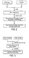
- Figure 2 schematically illustrates steps in the preparation of one type of coating solution for the deposition of YSZ (Yttria Stabilised Zirconia).
- a precursor compound in this case, Zr(OC 4 H 9 ) 4
- a solvent in this case, Butanol - C 4 H 9 OH.
- This solution is stirred and a second precursor compound Y(O 2 C 4 H 15 ) 3 (more generally, a metal alkoxide or an organometallic compound) is added under action of heat.
- the mixture is then catalysed to form a coating solution of the desired pH.
- ethanoic acid CH 3 COOH
- other acids such as HCI
- alkalis such as NH 3
- the desired pH may be between 2 and 5.
- the desired pH may be between 9 and 12.
- the coating solution a mixture of Zr(OC 4 H 9 ) 4 , Butanol and Y(O 2 C 4 H 15 ) 3 , is then passed to the outlet 5 and discharged towards the substrate 14.
- the concentration of the desired coating solution is approximately 0.01-0.5 mol/l (moles per litre).
- the coating solution may have a viscosity in the region of about 0.01 to 50 mPa.S (millipascal seconds) depending on the type of film that it is desired to produce.
- Table 1 shows the compositions of coating solutions for various deposited films.
- the composite precursors with alkoxide precursors are so-called "sol" precursors 1 .
- the precursor compounds are mixed in relative quantities appropriate to the desired stoichiometry of the desired film.
- Sufficient catalyst is added to give the coating solution the required pH.
- Ethanoic Acid is a preferred catalyst to provide a clear solution, an improved solution conductivity and therefore finer spray droplets.
- other acids and/or alkalis such as hydrochloric acid, ammonia, nitric acid, Lewis acid or sodium hydroxide would all be suitable catalysts.
- Acid or base catalysts can influence both the hydrolysis and condensation rates and the structures of the condensed products. Acids serve to protonate negatively charged alkoxide groups, enhancing the reaction kinetics and eliminating the requirement for proton transfer within the transition site. Therefore, acid-catalysed condensation is directed preferentially towards the ends rather than the middles of chains, resulting in more extended, less highly branched polymers. Alkaline conditions produce strong nucleophiles via deprotonation of hydroxo ligands. Base-catalysed condensation (as well as hydrolysis) should be directed toward the middles rather than the ends of chains, leading to more compact, highly branched species. Hence, if porous films of good quality (e.g. adhesion and porosity) are required, alkalis are preferred as catalysts.
- good quality e.g. adhesion and porosity
- inorganic or organic solvents can be used such as alcohol, water, or a mixture of alcohol and water could be used.
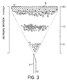
- Figure 3 schematically illustrates the principle of electrostatic spray assisted vapour deposition of a film from a coating solution.
- the temperature preferably increases, on passing from the outlet to the substrate, from about 100°C to between 400 and 650°C.
- the coating solution forms a corona spray, the droplets of which are charged to a positive potential.
- the droplets As the droplets are attracted to the substrate 14 they begin to form clusters together (shown at point (II) in Figure 3) under the influence of an increased ambient temperature.
- the clusters decompose and/or react in close proximity to the substrate to form the desired ceramic film.
- the clusters may also react with other gaseous reactants such as oxygen.
- hydrolysis/condensation reaction for the production of a Sol ⁇ gel transition is as follows: Hydrolysis ⁇ M-OR + H 2 O ⁇ ⁇ M-OH + ROH Condensation ⁇ M-OH + RO-M ⁇ ⁇ ⁇ M-O-M ⁇ + ROH ⁇ M-OH + HO-M ⁇ ⁇ ⁇ M-O-M ⁇ + H 2 O
- M is the desired metal film element (in this case of YSZ, Zirconium) and R is C n H 2n+1 , e.g. C 4 H 9 .
- the chemical reaction proceeds forwards (towards the right hand side of the above equations) and the reaction time decreases, with increasing temperature.
- the hydrolysis/condensation reaction is speeded up with increasing temperature.
- the substrate and other pieces of apparatus are open to the surrounding ambient atmosphere, and so the other ambient gaseous reactants refer to any other gaseous reactants (such as oxygen) that may be found in the atmosphere.
- the technique may be performed within the confines of a container, and any desired ambient gaseous reactants (such as hydrogen sulphide, for example) may be introduced into that container. These introduced gases may react with the clusters to form particular films (such as sulphide or nitrite films, for example) on the substrate.
- this method operates on a principle whereby charged droplets from the outlet 5 are attracted towards a grounded substrate, it is particularly suitable for scanning or writing large surface areas and is not restricted to particular chamber sizes as in CVD and PVD. Growth rates achievable with this method were found to be between 0.1 and 5 microns per minute depending upon the concentration and flow rate of coating solution. Higher growth rates are possible by further altering the deposition conditions.
- the achievable microstructure, grain size, composition, surface morphology and thickness of ceramic film are strongly dependant on the process conditions.
- the grain size in the deposited film is mainly determined by the droplet size, and the flow rate, viscosity and concentration of coating solution and substrate temperature.
- the grain size of ceramic films increases and uniformity of the grain distribution decreases as the droplet sizes, flow rates, concentration, substrate temperature and viscosity of coating solution increase.
- droplet sizes are mainly determined by the corona field intensity and coating liquid conductivity. The mean droplet size decreases with increasing coating liquid conductivity.
- the crystal phase structures of the deposited ceramic films are mainly determined by the temperature of the substrate 14. Ceramic films formed at lower substrate temperatures, have an amorphous or nanocrystalline crystal phase. These films may then be treated by an additional sintering process, to transform the crystal structure from an amorphous or nanocrystalline structure to the desired ceramic phase. A higher substrate temperature during deposition results in an increase in crystallinity of the ceramic film deposited thereupon.
- films such as simple oxide films, multicomponent oxide films (e.g. PZT (Lead Zirconate Titanate - Pb(Zr x Ti 1-x )O 3 ), PbTiO 3 , BaTiO 3 , Indium Tin Oxide or La(Sr)MnO 3 ) or doped films (e.g. YSZ (Yttria Stabilised Zirconia - (ZrO 2 ) 0.92 (Y 2 O 3 ) 0.08 ) or Ni-YSZ) etc, structural and/or functional films such as electroceramic films, nanostructured films, and/or of course films other than ceramics, may be produced with this technique.
- PZT Lead Zirconate Titanate - Pb(Zr x Ti 1-x )O 3
- PbTiO 3 BaTiO 3
- Indium Tin Oxide or La(Sr)MnO 3 or doped films
- YSZ Yttria Stabilised Zirc
- the uniformity of coating thickness can be improved by rotating and/or translating (in general, moving) the outlet and/or the substrate holder during deposition to vary the relative positions of the outlet and the substrate with time. If rotary motion is used, this could involve, for example, rotating the substrate (which might be three-dimensional) about an axis passing through the substrate, or possibly rotating the outlet (or outlets, if more than one is used) about an axis which is not coaxial with the outlet's axis (i.e. "circling" the outlet around).
- the polarity of the electric field applied between the outlet and the substrate holder can be reversed from time to time during the deposition process. This can be beneficial to avoid the accumulation of charges (which can counteract the effect of the applied field), thus allowing thicker coatings to be produced.
- “Graded” coatings can be produced by varying the concentration and/or composition of the precursor solution during deposition. (Simply, this can be achieved by depositing the contents of a first container (bottle) of precursor solution, and then switching to another container and so on).
- films may be produced of a thickness varying from a nanometre to approximately 100 micrometers in thickness (or much thicker).
- the coatings can be used in microscale circuitry or for much bulkier items such as turbine blades for jet engines, by scaling up the apparatus (the apparatus of Figures 1 and 4 as shown has a substrate diameter of about 20mm).
- Single crystal substrates can be used to obtain oriented or epitaxial films.
- a range of microstructures including epitaxial, columnar and equiaxial growth are possible by varying the processing conditions.
- the substrates may be conductive (e.g. metal) or non-conductive (e.g. glass, polymer or ceramic).
- EAVD electrostatic spray assisted vapour deposition
- the apparatus of Figure 4 is similar to that of Figure 1, except that a shaped substrate holder 104 projects towards the outlet 5 at either side of the substrate 14'.
- the substrate holder 104 is heated as before, and this heating serves to set up a temperature gradient whereby the ambient temperature increases as the substrate 14' is approached from the direction of the outlet 5.
- the arrangement of Figure 1 also provided an increase in temperature approaching the substrate 14' from the direction of the outlet 5, but the arrangement of Figure 4, with the projecting parts of the substrate holder 104, provides a more gradual temperature gradient). This increased temperature and more gradual temperature gradient facilitates solvent evaporates and decomposition of the coating solution near the vicinity of the substrate that enables deposition of the film.
- Plasma surface treatment techniques have been used widely in polymer industry.
- the techniques of flame treatment, acid etching, and corona discharge treatment after the fabrication of the bulk polymer materials have been used extensively in industrial applications, produce a variety of new polar surface. This is quite acceptable in wetting and printing applications, but for applications of polymers in electronic and biomedical devices, the presence of a polar surface is not sufficient.
- the alignment of polar groups in polymer films along preferred orientation need to be considered as well.
- Plasma surface treatment techniques have the advantage for the surface modification of commodity polymer substrates, but the penetration depth of the treatment is very low at a reaction level for useful surface modification. Meanwhile, the equipment of plasma technique is very expensive and needs highly skilled technicians.
- PVDF film has a large dielectric constant, due to the large dipole moment of CF 2 , and is one of the most polar dielectric polymers. Its advantages over ceramic materials include light weight, flexibility, toughness, ease of fabrication and low permittivity.
- the conventional fabrication of PVDF films for electronic application normally involves two production steps. Firstly, PVDF bulk films are produced by a conventional method such as cast, hot pressing, dipping and spin coating of PVDF solution. Then, PVDF bulk films are treated by the modification techniques such as high thermal high voltage poling, corona poling, stretching and electron beam discharge etc.
- the deposited PVDF films cannot be stretched, it is difficult to prepare ⁇ -phase crystal film by this method.
- the breakdown of thin films occurs easily under a high electric field. As a result, it is not easy to pole thin PVDF films.
- the film production and surface modification poling of polymer PVDF films can be achieved in.a single production step.
- the outlet's inner diameter preferably reduces towards the outlet's tip from about 1mm to about 0.1mm. This relatively large initial inner diameter ensures that the likelihood of clogging problems with high viscosity solutions (such as PVDF) in the outlet 5 is significantly reduced.
- a substantially constant flow of PVDF coating liquid to the outlet 5 is maintained by use of a syringe or pneumatic pump (not shown).
- the solution flow is in the range of 0.4 - 10 ml/h.
- the electrostatic field set up between the charged outlet 5 and substrate holder 104 serves to guide charged coating solution droplets to the substrate 14'.
- droplets of the coating solution are provided with a negative charge by way of the high voltage DC source 1. These negatively charged droplets are thus attracted onto the substrate and in moving towards the substrate pass through a region of increasing temperature gradient.
- the temperature gradient ensures that the solvent evaporates before the PVDF precursor droplets reach the substrate 14' and the chemical reaction occurs just on or in very close vicinity of the substrate surface to form a PVDF crystal phase film coating.
- the syringe pump can be turned off and heating can be stopped.
- the PVDF film coated substrate is then cooled down up to room temperature, with the electric field maintained during this cooling process.
- Figure 5 is a flow chart illustrating steps in a polymer deposition process.
- a precursor solution used to deposit the films of PVDF comprises a mixture of poly vinylidene fluoride (PVDF) powder and solvent N,N,-Dimethylformamide (DMF) or N,N,-Dimethylacetamide (DMA).
- PVDF powders are dissolved in DMA or DMF solvent. This solution is stirred and heated at 60°C for thirty minutes. A clear solution with 0.01 to 0.1M concentration in PVDF is yielded. Then, acetic acid CH 3 COOH is added into the solution as catalyst according to pH 2 to 5 and conductivity range greater than or equal to 2.0 ⁇ s at room temperature. After thirty minutes stirring, a clear precursor solution for PVDF film coating is obtained.
- PVDF films into a second crystal phase called ⁇ -phase in which the chain conformation is essentially all trans and the chains crystallized in an orthorhombic unit cell with a net dipole moment.
- the present process uses the inventors' observation that molecular dipoles on chains within the crystalline regions of the polymer become aligned with the applied electric field during the poling process and are then relatively stable in such an orientation in the absence of the piezo- and pyro electric response. Only the crystalline regions of the polymer would become permanently aligned and then only that component of the chain axis which lies in the plane of the film would be expected to contribute to the polarisation.
- X-ray diffraction patterns of the PVDF film produced under process I and process II are shown in Figures 6a and 6b respectively.
- the diffraction peak observed at 2 ⁇ 20.8° is assigned to unresolved (110) and (200) diffraction of ⁇ -phase in PVDF.
- ⁇ -phase in PVDF shows diffraction peaks 2 ⁇ 18° assigned to (100), (020) and (021) respectively.
- the comparison of process I with process II shows that the intensity of main peak at about 20.8° increases under corona field. It indicates that some parts of ⁇ -phase have transformed into ⁇ -phase in PVDF.
- the ⁇ - and ⁇ -phase crystal forms have many common absorption band characteristics (such as CH,CH 2 , CF,CF 2 , and C-C etc.) as reported in the literature. It is known that the crystal forms can be identified by the characteristic absorption bands of ⁇ -phase at about 510 and about 1280 cm -1 , and that of ⁇ -phase at about 530, about 610 and about 795 cm -1 .
- Figures 9a and 9b are schematic diagrams showing dipole orientation in polymer films produced by the two process variants, process I and process II. These illustrate that under process II a PVDF film with oriented ⁇ -phase crystal is obtained, which is very important for getting good piezoelectricity and pyroelectricity in PVDF film.
- the present studies thus show that the oriented thin PVDF film can be prepared directly onto a substrate in a single step by a novel ESAVD technique.
- the corona field is maintained during substrate cooling to form oriented polar polymer film PVDF, but other forms of PVDF can be produced without maintaining the field.
- the corona field helps to transport the charge droplets of PVDF solution onto the substrate to form PVDF thin film, and forces the polar group in PVDF thin film to align along the corona field.
- This technique can be used in the fabrication of a wide range of polymer films, including polar and conductive polymer/or co-polymer coatings, such as PVDF, PTFE, polyanilines, and polypyrrole etc.
- Figure 10 illustrates a third embodiment of a deposition apparatus.
- the apparatus of Figure 10 is similar to that of Figure 4, but for the addition of deflectors 210 under the control of a deflection controller 200.
- the deflectors are used to deflect the spray of electrically charged droplets emerging from the outlet. This can steer or concentrate the spray on particular desired areas of the substrate, or move the spray distribution around to help to compensate for an uneven temperature gradient near the substrate.
- the deflectors can be electrostatic plates, in which case the deflection controller supplies a high voltage between the plates to deflect the electrically charged spray emerging from the outlet, and/or magnetic deflectors (eg a yoke coil or other winding), in which case the deflection controller supplies a current to coils in the deflectors to generate a magnetic field to deflect the charged spray.
- the substrate could be heated to a temperature just below that required for film deposition (e.g. 50°C below that required for film deposition). If a laser beam is then directed onto the substrate by a suitable beam-steering mechanism and used to heat very localised areas of the substrate while the solution is being sprayed from the outlet, deposition will occur selectively at those areas of the substrate.
- masking can be used to mask off certain areas of the substrate to give control over where the film is deposited.
- Figures 11 to 14 relate to the use of these techniques to generate powders, rather than films or coatings.
- the example to be described is that of YSZ powders, but many other materials (particularly the materials described above with reference to the film or coating techniques) could be used.
- the differentiation between film (coating) production and powder production is mainly one of temperature (although other operational parameters can be varied). If the ambient temperature between the outlet and the substrate is increased then the droplets of coating solution will tend to form powder particles before hitting the substrate. This effect can be exaggerated by slowing down the flight of the droplets - e.g. by changing the flow rate or the electric field - to give more time for the powder to form. Alternatively, if a cold substrate is used, then the droplets will condense into powder particles on hitting the substrate.
- FIG 11 illustrates a suitable apparatus for manufacturing the powdered YSZ.
- the apparatus comprises a tubular, up-flow reactor equipped with an external resistive heater.
- YSZ sol precursor is delivered at an appropriate flow into a stainless steel capillary outlet (100 ⁇ m inside diameter, 650 ⁇ m outside diameter) which is maintained at a dc voltage of 10-30kV (positive polarity).
- the capillary electrode is placed 15-30 mm from a ring electrode maintained at 1kV dc voltage.
- the function of the ring electrode is to focus the spray aerosol into the reactor chamber and select the appropriate nanosized particles to reach the substrate.
- the high local electrostatic field at the capillary tip causes an emission of charged aerosol from the highly deformed liquid interface.
- a stream of Argon gas from a coaxial glass capillary (800 ⁇ m inside diameter) carries the spray charged aerosol through the ring electrode into the reaction zone of the reactor, finally to arrive at the cold substrate (having a negative polarity).
- the YSZ sol precursor with monodispersed nanosize particles is synthesized as follows. First, Y(NO 3 ) 3 .6H 2 O is dissolved in 2-propanol while stirring for about 15 min at room temperature yielding a clear solution. Zirconium tetra n-butoxide, Zr(OC 3 H 9 ) 4 is added into the previous solution according to the stoichiometry of a desired final composition of (ZrO 2 ) 0.92 (Y 2 O 3 ) 0.08 . The final sol precursor concentration and pH are preferably 0.05M and 3-5 respectively. The hydrolysis and condensation can be carried out at room temperature under stirring.
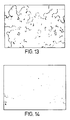
- the YSZ nanoparticles produced by a prototype of this technique were analysed using x-ray diffraction and transmission electron microscopy (TEM).
- Figures 13 and 14 show the microstructures of YSZ nanopowders at different reaction temperatures.
- the YSZ aerosol is produced by electrostatic assisted spray, and delivered into the reaction zone in a CVD reactor chamber, with the fine droplets of aerosol being converted into dry gel and pyrolysing to form the nanopowders on the cold substrate under an appropriate low temperature.
- TEM micrographs reveal that the distribution of YSZ nanoparticles is uniform and the average size of YSZ powders deposited at 500°C is 10-20 nm ( Figure 13). Under the high reaction temperature (e.g. 800 °C), particle-cluster aggregation occurs.
- TEM micrographs reveal that the distribution of YSZ nanoparticles is not uniform and the YSZ particle size is in the range of 30-80 nm at high temperatures ( Figure 14).
Abstract
Description
- This invention relates to film or coating deposition and powder formation.
- Ceramic, polymer and other films, coatings and powders are used in, for example, structural and functional electronic applications.
- As background, the distinction between a film and a coating is very loosely defined and is not important to the operation or description of the present invention. In one definition, a film would be considered as a layer under about 10 µm thick, and a coating would be of greater thickness. In the present description, however, the terms are generally used interchangeably.
- The following are examples of previously proposed techniques for generating such films, coatings and powders: physical vapour deposition (PVD) (a generic term given to a variety of sputtering techniques such as radio frequency (RF) sputtering, reactive magnetron sputtering and ion beam sputtering); flame spray deposition (FSD); the so-called sol-gel process; electrostatic spray pyrolysis (ESP); and chemical vapour deposition (CVD). Two particular examples are disclosed in EP-A-0 103 505 and Applied Physics Letters, Vol. 67, No. 22, Nov. 1995, pp 3337-3339.
- US-A-5344676 discloses a method and apparatus for producing nanodrops which are liquid drops with diameters of less than one micron and producing therefrom solid nanoparticles and uniform and patterned film deposits.
- US-A-4921731 discloses a method of ceramic coating a substrate by thermodeposition from a sol made by hydrolyzing and peptizing organometallic compounds in water.
- US-A-5298277 discloses a coating method in which a spray gun is moved along a locus in a direction transverse to the conveying direction of a workpiece.
- However, none of these techniques has been found to provide good control of the stoichiometry, morphology, microstructure and properties of multicomponent oxide films and a relatively high growth rate and deposited area of a deposited film. Also, the CVD and PVD techniques tend to need expensive equipment and highly skilled technicians for effective operation.
- Accordingly, the present invention provides a method of depositing a material onto a substrate, the method comprising the steps of: pressure feeding a material solution comprising one or more precursor compounds, a solvent and a pH-modifying catalyst from a material solution supply to an outlet; generating an electric field between the outlet and a substrate to provide a corona spray of droplets of the material solution and electrostatically attract the droplets from the outlet towards the substrate; and providing a decreasing temperature gradient from the surface of the substrate to the outlet.
- Further respective aspects of the invention (to which the various preferred features are equally applicable) are defined in the appended claims.
- Embodiments of this method, which will be referred to hereinafter as electrostatic spray assisted vapour deposition (ESAVD), enable the fabrication of both thin and thick films. The technique combines the advantages of CVD and electrostatic spray deposition whilst alleviating the problems associated therewith. In comparison to other film deposition techniques, ESAVD has a high deposition rate and efficiency, and allows easy control of the stoichiometry and microstructure of the deposits. In addition, it is a simple, cheap, and low-temperature synthesis method suitable for the fabrication of a variety of different films. The method also allows the deposition of a film on large surface area substrates.
- The use of the pH-modifying catalyst (which can be acid or alkali) can provide a clearer solution with increased electrical conductivity, and so can give finer droplets and thus a better coating quality.
- The method can be performed in so that the substrate and other pieces of apparatus are open to the surrounding ambient atmosphere, the other ambient gaseous reactants refer to any other gaseous reactants (such as oxygen, for example) that may be present in the atmosphere. In another embodiment, the method may performed within the confines of a container and said other ambient gaseous reactants may be supplied to said container, thereby to enable the deposition of a particular film.
- Both simple and multicomponent ceramic oxide films have been fabricated using the above mentioned method. In one embodiment, the film may be a ceramic film such as PZT (Lead Zirconate Titanate) or a doped film such as YSZ (Yttria Stabilised Zirconia). Other films may include PbTiO3, BaTiO3, La(Sr)MnO3, NiO-YSZ, SnO2-In2O3 and other Indium-Tin Oxide films. The film may also be a structural and/or functional film such as an electroceramic film.
- Preferably, the droplets are charged to a voltage within the approximate range 5-30 kilovolts with respect to the substrate.
- In one embodiment, the temperature increases gradually to a temperature in the
approximate range 100 to 650 degrees celsius (the temperature used may depend on the type of coating). Varying the processing parameters enables the production of dense/porous and/or thin/thick films all of which have good adhesion to the substrate. - Preferably, the film has a thickness between a nanometre and approximately 100 micrometers, or much thicker.
- In any of the above embodiments, the catalyst may be an acid such as ethanoic acid or hydrochloric acid. In this case, the required pH may be between 2 and 5.
- Alternatively, the catalyst may be an alkali such as NH3. In this case, the required pH may be between 9 and 12.
- The invention can be particularly useful for producing polymer coatings, in which case it is preferred that the electric field is maintained during at least part of the time during which the substrate cools down after coating has been performed. This can urge the polymer into a desirable polar structure.
- The invention will now be described, by way of example only, with reference to the accompanying drawings in which:
- Figure 1 illustrates schematically an apparatus for use in electrostatic spray assisted vapour deposition of a film on a substrate;
- Figure 2 is a flow chart that illustrates schematically steps in the synthesis of coating solution for the electrostatic spray assisted vapour deposition of YSZ:
- Figure 3 schematically illustrates the principle of electrostatic spray assisted vapour deposition of a film from a coating solution using the apparatus of Figure 1;
- Figure 4 schematically illustrates another embodiment of apparatus for use in electrostatic spray assisted vapour deposition;
- Figure 5 is a flow chart illustrating steps in a polymer deposition process;
- Figures 6a and 6b illustrate X-ray diffraction patterns for polymer films produced by two process variants;
- Figures 7a and 7b illustrate transmittance infra-red spectra for polymer films produced by the two process variants;
- Figures 8a and 8b illustrate surface reflectance infra-red spectra for polymer films produced by the two process variants;
- Figures 9a and 9b are schematic diagrams showing dipole orientation in polymer films produced by the two process variants;
- Figure 10 schematically illustrates a third embodiment of apparatus for material deposition;
- Figure 11 illustrates a fourth embodiment, used for powder deposition;
- Figure 12 (curves A and B) show x-ray diffraction patterns for the nano-powders produced at 500°C and 800°C respectively; and
- Figure 13 and 14 show the microstructures of YSZ nanopowders at different reaction temperatures.
-
- In a first embodiment a coating solution is deposited to form a ceramic film on a substrate.
- A film deposition apparatus as shown schematically in Figure 1 comprises an outlet (e.g. a nozzle, spray or similar) 5 connected to a high voltage DC source 7 preferably variable in the range 0-30 kV. In operation, a voltage of between 5 and 30 KV would be normally used for the apparatus as shown. A
substrate holder 4 is earthed and is heated by aheater 2. The temperature of thesubstrate holder 4 is controlled by thecontroller 1 and an attachedthermocouple 3. - Heating the substrate holder also causes a corresponding heating of the area surrounding the
substrate 14 and between the substrate holder and theoutlet 5. This heating serves to set up a temperature gradient whereby the ambient temperature increases as the substrate is approached from the direction of the outlet. This increasing temperature facilitates a chemical vapour reaction (see Figure 3) of the coating solution that enables deposition of the ceramic film. - When an electric field of sufficient strength is applied to the
outlet 5, a corona field is produced from the tip of theoutlet 5. A ceramic coating liquid is used to form the films and is fed into theoutlet 5 in the direction indicated by anarrow 6. - The outlet's inner diameter can vary from 1mm (millimeter) to 0.1mm. This relatively large inner diameter reduces the chances of clogging problems when high viscosity solutions are passed through the
outlet 5. - A substantially constant flow in the range of 0.4 - 60 ml/h (millilitres per hour) is maintained by use of a syringe pump or a constant static pressure feed.
- In this way, the electrostatic field set up between the
charged outlet 5 and theearthed substrate holder 4 serves to guide charged coating solution droplets to thesubstrate 14. Droplets of the coating solution are provided with a positive charge by way of the high voltage DC source 7. These positively charged droplets are attracted to the earthedsubstrate holder 4. (As an alternative, of course, the droplets could be negatively charged with anearthed holder 4, or vice versa). - Figure 2 schematically illustrates steps in the preparation of one type of coating solution for the deposition of YSZ (Yttria Stabilised Zirconia). First, a precursor compound (in this case, Zr(OC4H9)4 ) is mixed with a solvent (in this case, Butanol - C4H9OH). This solution is stirred and a second precursor compound Y(O2C4H15)3 (more generally, a metal alkoxide or an organometallic compound) is added under action of heat. The mixture is then catalysed to form a coating solution of the desired pH. In this case, ethanoic acid (CH3COOH) is used as a catalyst, but other acids (such as HCI) or alkalis (such as NH3) may be used in the preparation of alternative coating solutions. In the case of acid catalysed reactions, the desired pH may be between 2 and 5. In the case of alkali catalysed reactions, the desired pH may be between 9 and 12.
- The coating solution, a mixture of Zr(OC4H9)4, Butanol and Y(O2C4H15)3, is then passed to the
outlet 5 and discharged towards thesubstrate 14. - Preferably, the concentration of the desired coating solution is approximately 0.01-0.5 mol/l (moles per litre). In addition, the coating solution may have a viscosity in the region of about 0.01 to 50 mPa.S (millipascal seconds) depending on the type of film that it is desired to produce.
- Table 1 shows the compositions of coating solutions for various deposited films.

- In table 1, the composite precursors with alkoxide precursors are so-called "sol" precursors1. The precursor compounds are mixed in relative quantities appropriate to the desired stoichiometry of the desired film. Sufficient catalyst is added to give the coating solution the required pH.
- Ethanoic Acid is a preferred catalyst to provide a clear solution, an improved solution conductivity and therefore finer spray droplets. However, other acids and/or alkalis such as hydrochloric acid, ammonia, nitric acid, Lewis acid or sodium hydroxide would all be suitable catalysts.
- Acid or base catalysts can influence both the hydrolysis and condensation rates and the structures of the condensed products. Acids serve to protonate negatively charged alkoxide groups, enhancing the reaction kinetics and eliminating the requirement for proton transfer within the transition site. Therefore, acid-catalysed condensation is directed preferentially towards the ends rather than the middles of chains, resulting in more extended, less highly branched polymers. Alkaline conditions produce strong nucleophiles via deprotonation of hydroxo ligands. Base-catalysed condensation (as well as hydrolysis) should be directed toward the middles rather than the ends of chains, leading to more compact, highly branched species. Hence, if porous films of good quality (e.g. adhesion and porosity) are required, alkalis are preferred as catalysts.
- Similarly, various other inorganic or organic solvents can be used such as alcohol, water, or a mixture of alcohol and water could be used.
- Figure 3 schematically illustrates the principle of electrostatic spray assisted vapour deposition of a film from a coating solution.
- The temperature preferably increases, on passing from the outlet to the substrate, from about 100°C to between 400 and 650°C. At point (I) on Figure 3, the coating solution forms a corona spray, the droplets of which are charged to a positive potential. As the droplets are attracted to the
substrate 14 they begin to form clusters together (shown at point (II) in Figure 3) under the influence of an increased ambient temperature. At point (III) in Figure 3, the clusters decompose and/or react in close proximity to the substrate to form the desired ceramic film. The clusters may also react with other gaseous reactants such as oxygen. For example, the hydrolysis/condensation reaction for the production of a Sol→gel transition is as follows:Hydrolysis ≡M-OR + H2O ⇄ ≡M-OH + ROH Condensation ≡M-OH + RO-M≡ ⇄ ≡M-O-M≡ + ROH ≡M-OH + HO-M≡ ⇄ ≡M-O-M≡ + H2O - Where M is the desired metal film element (in this case of YSZ, Zirconium) and R is CnH2n+1, e.g. C4H9. In this method, the chemical reaction proceeds forwards (towards the right hand side of the above equations) and the reaction time decreases, with increasing temperature. Thus, the hydrolysis/condensation reaction is speeded up with increasing temperature.
- The substrate and other pieces of apparatus are open to the surrounding ambient atmosphere, and so the other ambient gaseous reactants refer to any other gaseous reactants (such as oxygen) that may be found in the atmosphere. In another embodiment, the technique may performed within the confines of a container, and any desired ambient gaseous reactants (such as hydrogen sulphide, for example) may be introduced into that container. These introduced gases may react with the clusters to form particular films (such as sulphide or nitrite films, for example) on the substrate.
- To summarise, during ESAVD, droplets of coating solution are charged and then transform into clusters or fine particles between the
discharge outlet 5 and thesubstrate 14. This transformation occurs under the action of a corona field and an increasing temperature towards the substrate. These clusters and fine particles are then attracted to the substrate by virtue of the induced electric field. The temperature gradient is such that the clusters and other gaseous reactants coexist around thesubstrate 14. The precursor clusters undergo decomposition and/or chemical reaction with gaseous reactants just on or in very close proximity to the substrate surface. Chemical reactions involving coating precursor clusters cause the formation of the desired ceramic film - as illustrated in Figure 3. - As this method operates on a principle whereby charged droplets from the
outlet 5 are attracted towards a grounded substrate, it is particularly suitable for scanning or writing large surface areas and is not restricted to particular chamber sizes as in CVD and PVD. Growth rates achievable with this method were found to be between 0.1 and 5 microns per minute depending upon the concentration and flow rate of coating solution. Higher growth rates are possible by further altering the deposition conditions. - The achievable microstructure, grain size, composition, surface morphology and thickness of ceramic film are strongly dependant on the process conditions. The grain size in the deposited film is mainly determined by the droplet size, and the flow rate, viscosity and concentration of coating solution and substrate temperature. For example, the grain size of ceramic films increases and uniformity of the grain distribution decreases as the droplet sizes, flow rates, concentration, substrate temperature and viscosity of coating solution increase. Similarly, droplet sizes are mainly determined by the corona field intensity and coating liquid conductivity. The mean droplet size decreases with increasing coating liquid conductivity. Thus, films with nanosize grained microstructure can be deposited with the ESAVD technique.
- The crystal phase structures of the deposited ceramic films are mainly determined by the temperature of the
substrate 14. Ceramic films formed at lower substrate temperatures, have an amorphous or nanocrystalline crystal phase. These films may then be treated by an additional sintering process, to transform the crystal structure from an amorphous or nanocrystalline structure to the desired ceramic phase. A higher substrate temperature during deposition results in an increase in crystallinity of the ceramic film deposited thereupon. - Other films, such as simple oxide films, multicomponent oxide films (e.g. PZT (Lead Zirconate Titanate - Pb(ZrxTi1-x)O3 ), PbTiO3, BaTiO3, Indium Tin Oxide or La(Sr)MnO3) or doped films (e.g. YSZ (Yttria Stabilised Zirconia - (ZrO2)0.92(Y2O3)0.08 ) or Ni-YSZ) etc, structural and/or functional films such as electroceramic films, nanostructured films, and/or of course films other than ceramics, may be produced with this technique.
- Referring back to Figure 1, because the temperature gradient generated by the projections of the
substrate holder 4 towards theoutlet 5 is not necessarily constant in front of thesubstrate 14 in the plane of the substrate, the uniformity of coating thickness can be improved by rotating and/or translating (in general, moving) the outlet and/or the substrate holder during deposition to vary the relative positions of the outlet and the substrate with time. If rotary motion is used, this could involve, for example, rotating the substrate (which might be three-dimensional) about an axis passing through the substrate, or possibly rotating the outlet (or outlets, if more than one is used) about an axis which is not coaxial with the outlet's axis (i.e. "circling" the outlet around). - In another feature, the polarity of the electric field applied between the outlet and the substrate holder can be reversed from time to time during the deposition process. This can be beneficial to avoid the accumulation of charges (which can counteract the effect of the applied field), thus allowing thicker coatings to be produced.
- "Graded" coatings can be produced by varying the concentration and/or composition of the precursor solution during deposition. (Simply, this can be achieved by depositing the contents of a first container (bottle) of precursor solution, and then switching to another container and so on).
- Similarly, it has been found that films may be produced of a thickness varying from a nanometre to approximately 100 micrometers in thickness (or much thicker). The coatings can be used in microscale circuitry or for much bulkier items such as turbine blades for jet engines, by scaling up the apparatus (the apparatus of Figures 1 and 4 as shown has a substrate diameter of about 20mm).
- Single crystal substrates can be used to obtain oriented or epitaxial films. A range of microstructures including epitaxial, columnar and equiaxial growth are possible by varying the processing conditions.
- The substrates may be conductive (e.g. metal) or non-conductive (e.g. glass, polymer or ceramic).
- Another embodiment of an electrostatic spray assisted vapour deposition (ESAVD) apparatus is schematically illustrated in Figure 4.
- The apparatus of Figure 4 is similar to that of Figure 1, except that a
shaped substrate holder 104 projects towards theoutlet 5 at either side of the substrate 14'. Thesubstrate holder 104 is heated as before, and this heating serves to set up a temperature gradient whereby the ambient temperature increases as the substrate 14' is approached from the direction of theoutlet 5. (The arrangement of Figure 1 also provided an increase in temperature approaching the substrate 14' from the direction of theoutlet 5, but the arrangement of Figure 4, with the projecting parts of thesubstrate holder 104, provides a more gradual temperature gradient). This increased temperature and more gradual temperature gradient facilitates solvent evaporates and decomposition of the coating solution near the vicinity of the substrate that enables deposition of the film. - The use of the apparatus of Figure 4 (or indeed, Figure 1) to produce PVDF polymer coatings on the substrate will now be described.
- The improvement of the performance of polymer films, and the ability to fabricate specific bulk polymer with tailored surface compositions for particular application have become important considerations. The need for designing polymer with well-controlled chemical compositions at the surface arises from the fact that interfacial phenomena define properties that are crucial to the service performance of a particular device. Examples of applications where polymer surface properties are important include wetting, printing, biomedical and electronic devices. In all these cases, molecules from the "environment" approach the polymer surface and experience interfacial forces due to electrostatic and positive/or negative charged cloud interactions. It thus becomes possible, in principle, to design guided approaches towards device optimization by controlling polymer film growth in order to alter or control interfacial interactions of polymers by the provision of appropriate chemical structure in the surface layers.
- Surface modification techniques have been used widely in polymer industry. The techniques of flame treatment, acid etching, and corona discharge treatment after the fabrication of the bulk polymer materials have been used extensively in industrial applications, produce a variety of new polar surface. This is quite acceptable in wetting and printing applications, but for applications of polymers in electronic and biomedical devices, the presence of a polar surface is not sufficient. The alignment of polar groups in polymer films along preferred orientation need to be considered as well. Plasma surface treatment techniques have the advantage for the surface modification of commodity polymer substrates, but the penetration depth of the treatment is very low at a reaction level for useful surface modification. Meanwhile, the equipment of plasma technique is very expensive and needs highly skilled technicians.
- A typical example for the polymer depositions is to fabricate the piezoelectric and pyroelectric polyvinylidene fluoride (PVDF) film. PVDF film has a large dielectric constant, due to the large dipole moment of CF2, and is one of the most polar dielectric polymers. Its advantages over ceramic materials include light weight, flexibility, toughness, ease of fabrication and low permittivity. The conventional fabrication of PVDF films for electronic application normally involves two production steps. Firstly, PVDF bulk films are produced by a conventional method such as cast, hot pressing, dipping and spin coating of PVDF solution. Then, PVDF bulk films are treated by the modification techniques such as high thermal high voltage poling, corona poling, stretching and electron beam discharge etc. However, the deposited PVDF films cannot be stretched, it is difficult to prepare β-phase crystal film by this method. On the other hand, the breakdown of thin films occurs easily under a high electric field. As a result, it is not easy to pole thin PVDF films. In the present technique, the film production and surface modification poling of polymer PVDF films can be achieved in.a single production step.
- Therefore, in this application, the outlet's inner diameter preferably reduces towards the outlet's tip from about 1mm to about 0.1mm. This relatively large initial inner diameter ensures that the likelihood of clogging problems with high viscosity solutions (such as PVDF) in the
outlet 5 is significantly reduced. - A substantially constant flow of PVDF coating liquid to the
outlet 5 is maintained by use of a syringe or pneumatic pump (not shown). Preferably, the solution flow is in the range of 0.4 - 10 ml/h. - In this way, the electrostatic field set up between the charged
outlet 5 andsubstrate holder 104 serves to guide charged coating solution droplets to the substrate 14'. As described earlier, droplets of the coating solution are provided with a negative charge by way of the highvoltage DC source 1. These negatively charged droplets are thus attracted onto the substrate and in moving towards the substrate pass through a region of increasing temperature gradient. The temperature gradient ensures that the solvent evaporates before the PVDF precursor droplets reach the substrate 14' and the chemical reaction occurs just on or in very close vicinity of the substrate surface to form a PVDF crystal phase film coating. - After the PVDF film coating has been applied, the syringe pump can be turned off and heating can be stopped. The PVDF film coated substrate is then cooled down up to room temperature, with the electric field maintained during this cooling process.
- Figure 5 is a flow chart illustrating steps in a polymer deposition process.
- Referring to Figure 5, a precursor solution used to deposit the films of PVDF comprises a mixture of poly vinylidene fluoride (PVDF) powder and solvent N,N,-Dimethylformamide (DMF) or N,N,-Dimethylacetamide (DMA). As a first step, PVDF powders are dissolved in DMA or DMF solvent. This solution is stirred and heated at 60°C for thirty minutes. A clear solution with 0.01 to 0.1M concentration in PVDF is yielded. Then, acetic acid CH3COOH is added into the solution as catalyst according to
pH 2 to 5 and conductivity range greater than or equal to 2.0µs at room temperature. After thirty minutes stirring, a clear precursor solution for PVDF film coating is obtained. - Although there is no complete agreement among investigators regarding the mechanism responsible for piezoelectricity and pyroelectricity in PVDF, there is nearly unanimous agreement that a polar crystal form is required for optimum activity. One of the complicating factors about PVDF is that it can exist in four different crystal forms. The crystal phase in which the chain conformation is trans-gauche-trans-gauche is called α-phase. The chains are then packed in a monoclinic unit cell which is non-polar.
- A variety of techniques have been employed to form PVDF films into a second crystal phase called β-phase in which the chain conformation is essentially all trans and the chains crystallized in an orthorhombic unit cell with a net dipole moment.
- It is thus known that there are at least two stable crystal forms of PVDF, a T-G-T-G non-polar form (α-phase) and a planar zig-zag polar form (β-phase). One can obtain an oriented β-form from the α-form in PVDF films by mechanical stretching or rolling, corona discharge, and high temperature high voltage poling. A number of researchers have shown that the β-form is very important in obtaining good piezoelectricity and pyroelectricity in PVDF films.
- Since the β-form crystal exhibits a net dipole moment, the present process uses the inventors' observation that molecular dipoles on chains within the crystalline regions of the polymer become aligned with the applied electric field during the poling process and are then relatively stable in such an orientation in the absence of the piezo- and pyro electric response. Only the crystalline regions of the polymer would become permanently aligned and then only that component of the chain axis which lies in the plane of the film would be expected to contribute to the polarisation.
- For identifying the influence of corona field in trials of this process, in fact two experimental processes were compared. In the first case, the corona field was turned off while samples were cooled down to room temperature after deposition (process I). In the second case, the corona field was maintained while samples were cooled down to room temperature after deposition (process II), to maintain the dipole orientation of the deposited material in a required orientation until the material solidified.
- X-ray diffraction patterns of the PVDF film produced under process I and process II are shown in Figures 6a and 6b respectively. The diffraction peak observed at 2≈20.8° is assigned to unresolved (110) and (200) diffraction of β-phase in PVDF. α-phase in PVDF shows
diffraction peaks 2≈18° assigned to (100), (020) and (021) respectively. The comparison of process I with process II shows that the intensity of main peak at about 20.8° increases under corona field. It indicates that some parts of α-phase have transformed into β-phase in PVDF. This result was confirmed by respective infra-red (IR) spectra, as shown in Figures 7a (Process I) and 7b (Process II) for transmission spectra, and Figures 8a (Process I) and 8b (Process II) for reflectance spectra. - Many journal papers have reported on the crystal forms of PVDF from IR spectra. The α- and β-phase crystal forms have many common absorption band characteristics (such as CH,CH2, CF,CF2, and C-C etc.) as reported in the literature. It is known that the crystal forms can be identified by the characteristic absorption bands of β-phase at about 510 and about 1280 cm-1, and that of α-phase at about 530, about 610 and about 795 cm-1.
- From the results of IR analysis between process I and II, it is clear that the contents of β-phase is higher in the PVDF film produced using process II, but a certain amount of α-phase may still exist under process II. It indicates that PVDF films prepared by process II consist mainly of the β crystal phase with some α-phase. Meanwhile, it is also found that corona field strongly influenced the surface structure of PVDF film. From the spectra, it is observed that since the absorption peak at about 1280 cm-1 in process II is assigned to the CF2 symmetric stretching vibration of β crystal phase, and is stronger than that in process I, the results of the IR spectra suggest that β-form crystal is oriented and the CF2 dipoles are aligned along the applied corona field.
- There have been many investigations of α-phase and β-phase crystal in PVDF film. It is well known that the α-phase crystal is more stable than the β-phase crystal. The reason why the β-phase crystal was formed in spite of its instability was not clear. In the present case of ESAVD, it is proposed that the stability and the mechanism of β-phase crystal formation is as follows. Because β-phase crystal is the polar crystal, β-phase is stabilized and formed in preference to α-phase when the corona field exist during the deposition of PVDF film. Consequently, the content of β-phase increases with increasing the energy supplied to the substrate by the corona discharge. Under the conditions shown in the experimental section, the charged droplets of the PVDF solution were attracted onto the substrate and the PVDF film was formed by evaporation of the solvent and decomposition of precursor solution during substrate temperature field. PVDF polymer seems to have enough mobility to change the conformation aligned along the applied field direction under the existence of the corona field during evaporation of the solvent. But if the corona field does not exist after deposition (as process I), a certain amount of energy is obtained to rearrange the PVDF molecules because the substrate temperature is high enough near/or over PVDF melting point 170°C. In contrast, when the corona field exists during cooling down of the PVDF film to room temperature, the polar groups in PVDF film are "cooled" along the applied corona field direction.
- Figures 9a and 9b are schematic diagrams showing dipole orientation in polymer films produced by the two process variants, process I and process II. These illustrate that under process II a PVDF film with oriented β-phase crystal is obtained, which is very important for getting good piezoelectricity and pyroelectricity in PVDF film.
- The present studies thus show that the oriented thin PVDF film can be prepared directly onto a substrate in a single step by a novel ESAVD technique. The corona field is maintained during substrate cooling to form oriented polar polymer film PVDF, but other forms of PVDF can be produced without maintaining the field. The corona field helps to transport the charge droplets of PVDF solution onto the substrate to form PVDF thin film, and forces the polar group in PVDF thin film to align along the corona field.
- In conclusion, the utilization of corona field in the vapour deposition process is effective in controlling crystal forms and their orientation, to form polar polymer films.
- The present results also clearly revealed the potential of this technique to deposit polymer thin film of good quality with very simple equipment. This technique can be used in the fabrication of a wide range of polymer films, including polar and conductive polymer/or co-polymer coatings, such as PVDF, PTFE, polyanilines, and polypyrrole etc.
- Figure 10 illustrates a third embodiment of a deposition apparatus. In many respects, the apparatus of Figure 10 is similar to that of Figure 4, but for the addition of
deflectors 210 under the control of adeflection controller 200. - The deflectors are used to deflect the spray of electrically charged droplets emerging from the outlet. This can steer or concentrate the spray on particular desired areas of the substrate, or move the spray distribution around to help to compensate for an uneven temperature gradient near the substrate. The deflectors can be electrostatic plates, in which case the deflection controller supplies a high voltage between the plates to deflect the electrically charged spray emerging from the outlet, and/or magnetic deflectors (eg a yoke coil or other winding), in which case the deflection controller supplies a current to coils in the deflectors to generate a magnetic field to deflect the charged spray.
- In other embodiments, the substrate could be heated to a temperature just below that required for film deposition (e.g. 50°C below that required for film deposition). If a laser beam is then directed onto the substrate by a suitable beam-steering mechanism and used to heat very localised areas of the substrate while the solution is being sprayed from the outlet, deposition will occur selectively at those areas of the substrate.
- In further alternative embodiments, masking can be used to mask off certain areas of the substrate to give control over where the film is deposited.
- Figures 11 to 14 relate to the use of these techniques to generate powders, rather than films or coatings. The example to be described is that of YSZ powders, but many other materials (particularly the materials described above with reference to the film or coating techniques) could be used.
- The differentiation between film (coating) production and powder production, using basically the same apparatus, is mainly one of temperature (although other operational parameters can be varied). If the ambient temperature between the outlet and the substrate is increased then the droplets of coating solution will tend to form powder particles before hitting the substrate. This effect can be exaggerated by slowing down the flight of the droplets - e.g. by changing the flow rate or the electric field - to give more time for the powder to form. Alternatively, if a cold substrate is used, then the droplets will condense into powder particles on hitting the substrate.
- Figure 11 illustrates a suitable apparatus for manufacturing the powdered YSZ. The apparatus comprises a tubular, up-flow reactor equipped with an external resistive heater. YSZ sol precursor is delivered at an appropriate flow into a stainless steel capillary outlet (100 µm inside diameter, 650 µm outside diameter) which is maintained at a dc voltage of 10-30kV (positive polarity). The capillary electrode is placed 15-30 mm from a ring electrode maintained at 1kV dc voltage. The function of the ring electrode is to focus the spray aerosol into the reactor chamber and select the appropriate nanosized particles to reach the substrate. The high local electrostatic field at the capillary tip causes an emission of charged aerosol from the highly deformed liquid interface. A stream of Argon gas from a coaxial glass capillary (800 µm inside diameter) carries the spray charged aerosol through the ring electrode into the reaction zone of the reactor, finally to arrive at the cold substrate (having a negative polarity).
- The YSZ sol precursor with monodispersed nanosize particles is synthesized as follows. First, Y(NO3)3.6H2O is dissolved in 2-propanol while stirring for about 15 min at room temperature yielding a clear solution. Zirconium tetra n-butoxide, Zr(OC3H9)4 is added into the previous solution according to the stoichiometry of a desired final composition of (ZrO2)0.92(Y2O3)0.08. The final sol precursor concentration and pH are preferably 0.05M and 3-5 respectively. The hydrolysis and condensation can be carried out at room temperature under stirring.
- The YSZ nanoparticles produced by a prototype of this technique were analysed using x-ray diffraction and transmission electron microscopy (TEM).
- The quality of the YSZ nanopowders depends strongly on the process conditions. Below a reaction temperature of 450°C, all samples appeared to be amorphous from the x-ray diffraction traces. Figure 12 (curves A and B) shows x-ray diffraction patterns for the nano-powders produced at 500°C and 800°C respectively. The x-ray diffraction patterns show that fully stabilized cubic zirconia (YSZ) nanopowders are directly formed. The presence of monoclinic or free Y2O3 phases was not detected in YSZ powders produced at about 500°C. No other new phases were observed. It indicates that Y2O3 has been perfectly dissolved into the ZrO2 lattice to form a solid solution.
- Figures 13 and 14 show the microstructures of YSZ nanopowders at different reaction temperatures. In the nanopowder formation process, the YSZ aerosol is produced by electrostatic assisted spray, and delivered into the reaction zone in a CVD reactor chamber, with the fine droplets of aerosol being converted into dry gel and pyrolysing to form the nanopowders on the cold substrate under an appropriate low temperature. TEM micrographs reveal that the distribution of YSZ nanoparticles is uniform and the average size of YSZ powders deposited at 500°C is 10-20 nm (Figure 13). Under the high reaction temperature (e.g. 800 °C), particle-cluster aggregation occurs. TEM micrographs reveal that the distribution of YSZ nanoparticles is not uniform and the YSZ particle size is in the range of 30-80 nm at high temperatures (Figure 14).
Claims (33)
- A method of depositing a material onto a substrate, the method comprising the steps of:pressure feeding a material solution comprising one or more precursor compounds, a solvent and a pH-modifying catalyst from a material solution supply to an outlet;generating an electric field between the outlet and a substrate to provide a corona spray of droplets of the material solution and electrostatically attract the droplets from the outlet towards the substrate; andproviding a decreasing temperature gradient from the surface of the substrate to the outlet.
- A method according to claim 1, wherein the step of generating an electric field comprises the step of:applying a voltage to the outlet such that droplets of the material solution emerging from the outlet are charged and attracted to the substrate by virtue of the electric field.
- A method according to claim 1 or claim 2, comprising the step of relatively rotating and/or translating the outlet and the substrate during the deposition process.
- A method according to any one of the preceding claims, comprising the step of varying the material solution composition and/or concentration during the deposition process.
- A method according to any one of the preceding claims, comprising the step of reversing the polarity of the electric field between the outlet and the substrate at intervals during the deposition process.
- A method according to any one of the preceding claims, comprising the step of locally heating areas of the substrate to enhance material deposition at the heated areas.
- A method according to any one of the preceding claims, comprising the step of electrostatically and/or magnetically steering the stream of droplets in transit from the outlet to the substrate.
- A method according to any one of the preceding claims, wherein the material is deposited as a film.
- A method according to claim 8, wherein the film is a multicomponent oxide film, a simple oxide film or a doped film.
- A method according to claim 8 or claim 9, wherein the film is one or more of a structural film, a functional film and an electroceramic film.
- A method according to any one of claims 1 to 7, in which the material is deposited as a powder.
- A method according to any one of the preceding claim, in which the material solution is a polymer solution.
- A method according to claim 12, comprising the step of maintaining the applied electric field for at least part of the time during which the material deposited on the substrate is allowed to cool.
- A method according to any one of the preceding claims, wherein the catalyst is an acid, added in sufficient quantity to give a material solution pH of between 2 and 5.
- A method according to claim 14, wherein the catalyst is selected from the group consisting of ethanoic acid and hydrochloric acid.
- A method according to any one of claims 1 to 13, wherein the catalyst is an alkali, added in sufficient quantity to give a material solution pH of between 9 and 12.
- A method according to claim 16, wherein the catalyst is NH3.
- A method according to any one of the preceding claims, wherein the droplets of material solution are charged to approximately 5 to 30 kV with respect to the substrate.
- A method according to any one of the preceding claims, wherein the temperature increases to a temperature in the approximate range from about 100 to about 650°C.
- A method according to any one of claims 1 to 18, wherein the temperature increases to a temperature in the approximate range from about 100 to about 400°C.
- A method according to any one of the preceding claims, wherein the method is performed within the confines of a container and gaseous reactants are supplied to the container to enable deposition of a film.
- A method according to any one of claims 1 to 11, wherein the material is Lead Zirconate Titanate (PZT), and the material solution is manufactured by the steps of:(a) mixing CH3OCH2CH2OH (solvent) with a first precursor compound Pb(CH3CO2)2 and Zr(OC3H7)4 and a second precursor compound Ti(OC3H7)4, and(b) adding a catalyst to the mixture to provide a material solution of a required pH.
- A method according to any one of claims 1 to 11, wherein the material is PbTiO3, and the material solution is manufactured by the steps of:(a) mixing CH3OCH2CH2OH (solvent) with a first precursor compound Pb(CH3CO2)2 and a second precursor compound Ti(OC3H7)4, and(b) adding a catalyst to the mixture to provide a material solution of a required pH.
- A method according to any one of claims 1 to 11, wherein the material is BaTiO3, and the material solution is manufactured by the steps of:(a) mixing CH3OCH2CH2OH (solvent) with a first precursor compound Ba(CH3CO2)2 and a second precursor compound Ti(OC3H7)4, and(b) adding a catalyst to the mixture to provide a material solution of a required pH.
- A method according to any one of claims 1 to 11, wherein the material is SnO2-In2O3, and the material solution is manufactured by the steps of:(a) mixing ethanol (solvent) with a first precursor compound In(NO3)3.xH2O and a second precursor compound SnCl2, and(b) adding a catalyst to the mixture to provide a material solution of a required pH.
- A method according to any one of claims 1 to 11, wherein the material is La(Sr)MnO3, and the material solution is manufactured by the steps of:(a) mixing about 20% H2O and about 80% ethanol (solvent) with a first precursor compound La(NO3)3.xH2O and Mn(NO3).6H2O and a second precursor compound SrNO3, and(b) adding a catalyst to the mixture to provide a material solution of a required pH.
- A method according to any one of claims 1 to 11, wherein the material is Yttria Stabilised Zirconia (YSZ), and the material solution is manufactured by the steps of:(a) mixing propanol or butanol (solvent) with a first precursor compound Y(O2C8H15)3 and a second precursor compound Zr(OC4H9)4, and(b) adding a catalyst to the mixture to provide a material solution of a required pH.
- A method according to any one of claims 1 to 11, wherein the material is Yttria Stabilised Zirconia (YSZ), and the material solution is manufactured by the steps of:(a) mixing propanol or butanol (solvent) with a first precursor compound Y(O2C8H15)3 and a second precursor compound Zr(OC3H7)4, and(b) adding a catalyst to the mixture to provide a material solution of a required pH.
- A method according to any one of claims 1 to 11, wherein the material is NiO-YSZ, and the material solution is manufactured by the steps of:(a) mixing propanol (solvent) with a first precursor compound Ni(NO3)2.6H2O and Zr(OC3H7)4 and a second precursor compound Y(O2C8H15)3, and(b) adding a catalyst to the mixture to provide a material solution of a required pH.
- A method according to any one of the preceding claims, wherein the film has a thickness between 1 nm and approximately 100 µm.
- A method according to any one of the preceding claims, wherein the substrate is disposed opposite the outlet.
- A method according to any one of the preceding claims, wherein the step of pressure feeding the material solution comprises the step of pumping the material solution.
- A method according to any one of the preceding claims, wherein the decreasing temperature gradient is such that evaporation of solvent from, and one or both of decomposition of and chemical reaction of, the droplets occurs as the droplets approach the surface of the substrate.
Applications Claiming Priority (7)
| Application Number | Priority Date | Filing Date | Title |
|---|---|---|---|
| GB9525505 | 1995-12-14 | ||
| GB9525505A GB2308132A (en) | 1995-12-14 | 1995-12-14 | Depositing films on a substrate using an electric field |
| GB9617248 | 1996-08-16 | ||
| GBGB9617248.1A GB9617248D0 (en) | 1995-12-14 | 1996-08-16 | A method of depositing films or coatings on a substrate |
| GB9619146A GB9619146D0 (en) | 1995-12-14 | 1996-09-13 | Powder synthesis |
| GB9619146 | 1996-09-13 | ||
| PCT/GB1996/003105 WO1997021848A1 (en) | 1995-12-14 | 1996-12-16 | Film or coating deposition and powder formation |
Publications (2)
| Publication Number | Publication Date |
|---|---|
| EP0870075A1 EP0870075A1 (en) | 1998-10-14 |
| EP0870075B1 true EP0870075B1 (en) | 2002-06-12 |
Family
ID=27268027
Family Applications (1)
| Application Number | Title | Priority Date | Filing Date |
|---|---|---|---|
| EP96942464A Expired - Lifetime EP0870075B1 (en) | 1995-12-14 | 1996-12-16 | Film or coating deposition and powder formation |
Country Status (7)
| Country | Link |
|---|---|
| US (3) | US6331330B1 (en) |
| EP (1) | EP0870075B1 (en) |
| AT (1) | ATE219165T1 (en) |
| AU (1) | AU1182997A (en) |
| CA (1) | CA2240625A1 (en) |
| DE (1) | DE69621826T2 (en) |
| WO (1) | WO1997021848A1 (en) |
Families Citing this family (87)
| Publication number | Priority date | Publication date | Assignee | Title |
|---|---|---|---|---|
| ATE219165T1 (en) * | 1995-12-14 | 2002-06-15 | Imperial College | FILM OR LAYER DEPOSITION AND POWDER PRODUCTION |
| US6116184A (en) | 1996-05-21 | 2000-09-12 | Symetrix Corporation | Method and apparatus for misted liquid source deposition of thin film with reduced mist particle size |
| US5997642A (en) * | 1996-05-21 | 1999-12-07 | Symetrix Corporation | Method and apparatus for misted deposition of integrated circuit quality thin films |
| JP3866328B2 (en) * | 1996-06-06 | 2007-01-10 | 富士重工業株式会社 | Vehicle peripheral three-dimensional object recognition device |
| GB9711080D0 (en) * | 1997-05-29 | 1997-07-23 | Imperial College | Film or coating deposition on a substrate |
| JP2001523889A (en) * | 1997-11-17 | 2001-11-27 | シメトリックス・コーポレーション | Method and apparatus for performing mist deposition of thin films |
| GB9725878D0 (en) | 1997-12-05 | 1998-02-04 | Imperial College | Vapour deposition |
| GB9800511D0 (en) | 1998-01-13 | 1998-03-11 | Rolls Royce Plc | A metallic article having a thermal barrier coating and a method of application thereof |
| US7713297B2 (en) | 1998-04-11 | 2010-05-11 | Boston Scientific Scimed, Inc. | Drug-releasing stent with ceramic-containing layer |
| GB9814191D0 (en) * | 1998-06-30 | 1998-08-26 | Imperial College | Vapour deposition |
| US20040197493A1 (en) * | 1998-09-30 | 2004-10-07 | Optomec Design Company | Apparatus, methods and precision spray processes for direct write and maskless mesoscale material deposition |
| US7045015B2 (en) | 1998-09-30 | 2006-05-16 | Optomec Design Company | Apparatuses and method for maskless mesoscale material deposition |
| US7108894B2 (en) * | 1998-09-30 | 2006-09-19 | Optomec Design Company | Direct Write™ System |
| US7938079B2 (en) | 1998-09-30 | 2011-05-10 | Optomec Design Company | Annular aerosol jet deposition using an extended nozzle |
| US7294366B2 (en) * | 1998-09-30 | 2007-11-13 | Optomec Design Company | Laser processing for heat-sensitive mesoscale deposition |
| US8110247B2 (en) | 1998-09-30 | 2012-02-07 | Optomec Design Company | Laser processing for heat-sensitive mesoscale deposition of oxygen-sensitive materials |
| GB9900955D0 (en) | 1999-01-15 | 1999-03-10 | Imperial College | Material deposition |
| JP2002316037A (en) * | 2001-04-11 | 2002-10-29 | Fukukoku Ko | Flame deposition and nonvacuum physical vapor deposition |
| DE10344135A1 (en) * | 2003-09-24 | 2005-05-04 | Karlsruhe Forschzent | Device for applying electro-spray coatings to electrically non-conducting surfaces has electrospray capillary for introducing, electrically charging electrospray onto surfaces, periodically repeats compensation, dissipation of charges |
| TWI242606B (en) * | 2003-09-26 | 2005-11-01 | Optomec Design | Laser treatment process for maskless low-temperature deposition of electronic materials |
| WO2005039814A2 (en) * | 2003-09-26 | 2005-05-06 | Optomec Design Company | Laser processing for heat-sensitive mesoscale deposition |
| DE10345738A1 (en) * | 2003-10-01 | 2005-05-04 | Deutsch Zentr Luft & Raumfahrt | Protection of metallic surfaces against thermally influenced wrinkling (Rumpling) |
| DE10349472B4 (en) * | 2003-10-21 | 2006-01-19 | Forschungszentrum Karlsruhe Gmbh | Coating device for polymers |
| US7252851B2 (en) * | 2003-11-04 | 2007-08-07 | Illinois Institute Of Technology | Method and apparatus for electrostatic spray deposition for a solid oxide fuel cell |
| US8166911B2 (en) * | 2003-11-04 | 2012-05-01 | Illinois Institute Of Technology | Method and apparatus for electrostatic spray deposition for a solid oxide fuel cell |
| US6991759B2 (en) * | 2003-12-10 | 2006-01-31 | Radhakrishnan Subramaniam | Process for preparation of semi-conducting polymer film containing beta crystalline phase of polyvinylidene fluoride |
| GB0416859D0 (en) * | 2004-07-29 | 2004-09-01 | Oxonia Ltd | Improved deposition process |
| US7259109B2 (en) * | 2004-09-22 | 2007-08-21 | Intel Corporation | Electrospray and enhanced electrospray deposition of thin films on semiconductor substrates |
| JP2006097087A (en) * | 2004-09-29 | 2006-04-13 | Fuji Photo Film Co Ltd | Film deposition method and film deposition apparatus |
| US20060280866A1 (en) * | 2004-10-13 | 2006-12-14 | Optomec Design Company | Method and apparatus for mesoscale deposition of biological materials and biomaterials |
| EP1820005B1 (en) * | 2004-11-24 | 2019-01-09 | Sensirion Holding AG | Method for applying selectively a layer to a structured substrate by the usage of a temperature gradient in the substrate |
| US7938341B2 (en) | 2004-12-13 | 2011-05-10 | Optomec Design Company | Miniature aerosol jet and aerosol jet array |
| US7674671B2 (en) | 2004-12-13 | 2010-03-09 | Optomec Design Company | Aerodynamic jetting of aerosolized fluids for fabrication of passive structures |
| US20080317967A1 (en) * | 2005-02-14 | 2008-12-25 | Kwang-Leong Choy | Deposition of Polymeric Films |
| WO2006089134A2 (en) * | 2005-02-15 | 2006-08-24 | Ehd Technology Group, Inc. | Apparatus and method for surface preparation using energetic and reactive cluster beams |
| PT103318B (en) * | 2005-07-19 | 2009-01-22 | Univ Do Minho | NON-POROUS FILMS IN THE BETA POLY PHASE (VINYLIDENE FLUORIDE) (PVDF) AND METHOD FOR THEIR PROCESSING |
| US8945684B2 (en) * | 2005-11-04 | 2015-02-03 | Essilor International (Compagnie Generale D'optique) | Process for coating an article with an anti-fouling surface coating by vacuum evaporation |
| CN100382350C (en) * | 2005-12-05 | 2008-04-16 | 浙江大学 | Porous composite thick film pyroelectric material and preparative method |
| US20070224235A1 (en) | 2006-03-24 | 2007-09-27 | Barron Tenney | Medical devices having nanoporous coatings for controlled therapeutic agent delivery |
| US8187620B2 (en) | 2006-03-27 | 2012-05-29 | Boston Scientific Scimed, Inc. | Medical devices comprising a porous metal oxide or metal material and a polymer coating for delivering therapeutic agents |
| US8815275B2 (en) | 2006-06-28 | 2014-08-26 | Boston Scientific Scimed, Inc. | Coatings for medical devices comprising a therapeutic agent and a metallic material |
| CA2655793A1 (en) | 2006-06-29 | 2008-01-03 | Boston Scientific Limited | Medical devices with selective coating |
| US20080051881A1 (en) * | 2006-08-24 | 2008-02-28 | Feng James Q | Medical devices comprising porous layers for the release of therapeutic agents |
| JP2010503469A (en) | 2006-09-14 | 2010-02-04 | ボストン サイエンティフィック リミテッド | Medical device having drug-eluting film |
| US7981150B2 (en) | 2006-11-09 | 2011-07-19 | Boston Scientific Scimed, Inc. | Endoprosthesis with coatings |
| US8431149B2 (en) | 2007-03-01 | 2013-04-30 | Boston Scientific Scimed, Inc. | Coated medical devices for abluminal drug delivery |
| US8070797B2 (en) | 2007-03-01 | 2011-12-06 | Boston Scientific Scimed, Inc. | Medical device with a porous surface for delivery of a therapeutic agent |
| US8067054B2 (en) | 2007-04-05 | 2011-11-29 | Boston Scientific Scimed, Inc. | Stents with ceramic drug reservoir layer and methods of making and using the same |
| US7976915B2 (en) | 2007-05-23 | 2011-07-12 | Boston Scientific Scimed, Inc. | Endoprosthesis with select ceramic morphology |
| US8002823B2 (en) | 2007-07-11 | 2011-08-23 | Boston Scientific Scimed, Inc. | Endoprosthesis coating |
| US7942926B2 (en) | 2007-07-11 | 2011-05-17 | Boston Scientific Scimed, Inc. | Endoprosthesis coating |
| WO2009012353A2 (en) | 2007-07-19 | 2009-01-22 | Boston Scientific Limited | Endoprosthesis having a non-fouling surface |
| US7931683B2 (en) | 2007-07-27 | 2011-04-26 | Boston Scientific Scimed, Inc. | Articles having ceramic coated surfaces |
| US8815273B2 (en) | 2007-07-27 | 2014-08-26 | Boston Scientific Scimed, Inc. | Drug eluting medical devices having porous layers |
| WO2009018340A2 (en) | 2007-07-31 | 2009-02-05 | Boston Scientific Scimed, Inc. | Medical device coating by laser cladding |
| JP2010535541A (en) | 2007-08-03 | 2010-11-25 | ボストン サイエンティフィック リミテッド | Coating for medical devices with large surface area |
| TWI482662B (en) | 2007-08-30 | 2015-05-01 | Optomec Inc | Mechanically integrated and closely coupled print head and mist source |
| TWI538737B (en) | 2007-08-31 | 2016-06-21 | 阿普托麥克股份有限公司 | Material deposition assembly |
| US8887658B2 (en) | 2007-10-09 | 2014-11-18 | Optomec, Inc. | Multiple sheath multiple capillary aerosol jet |
| US7938855B2 (en) | 2007-11-02 | 2011-05-10 | Boston Scientific Scimed, Inc. | Deformable underlayer for stent |
| US8216632B2 (en) | 2007-11-02 | 2012-07-10 | Boston Scientific Scimed, Inc. | Endoprosthesis coating |
| US8029554B2 (en) | 2007-11-02 | 2011-10-04 | Boston Scientific Scimed, Inc. | Stent with embedded material |
| EP2218513A1 (en) * | 2007-11-07 | 2010-08-18 | Fuence Co., Ltd. | Fixing machine |
| EP2271380B1 (en) | 2008-04-22 | 2013-03-20 | Boston Scientific Scimed, Inc. | Medical devices having a coating of inorganic material |
| WO2009132176A2 (en) | 2008-04-24 | 2009-10-29 | Boston Scientific Scimed, Inc. | Medical devices having inorganic particle layers |
| US20110171398A1 (en) * | 2010-01-12 | 2011-07-14 | Oladeji Isaiah O | Apparatus and method for depositing alkali metals |
| EP2303350A2 (en) | 2008-06-18 | 2011-04-06 | Boston Scientific Scimed, Inc. | Endoprosthesis coating |
| JP5338175B2 (en) * | 2008-07-28 | 2013-11-13 | 株式会社村田製作所 | Method for producing metal oxide ultrafine particles |
| US8231980B2 (en) | 2008-12-03 | 2012-07-31 | Boston Scientific Scimed, Inc. | Medical implants including iridium oxide |
| US8071156B2 (en) | 2009-03-04 | 2011-12-06 | Boston Scientific Scimed, Inc. | Endoprostheses |
| US8287937B2 (en) | 2009-04-24 | 2012-10-16 | Boston Scientific Scimed, Inc. | Endoprosthese |
| EP2314734A1 (en) * | 2009-10-20 | 2011-04-27 | Technische Universität Berlin | Method of producing porous metal oxide films using template assisted electrostatic spray deposition |
| GB2477117B (en) * | 2010-01-22 | 2014-11-26 | Univ Sheffield Hallam | Anticorrosion sol-gel coating for metal substrate |
| EP2582858A1 (en) * | 2010-06-21 | 2013-04-24 | Beneq OY | Apparatus and method for coating glass substrate |
| WO2012001210A1 (en) * | 2010-06-29 | 2012-01-05 | Beneq Oy | Apparatus and method for charging nanoparticles |
| JP4868475B1 (en) * | 2011-06-20 | 2012-02-01 | ムネカタ株式会社 | Method and apparatus for forming piezoelectric / pyroelectric film |
| JP2013207155A (en) * | 2012-03-29 | 2013-10-07 | Mitsubishi Materials Corp | Ferroelectric thin film manufacturing method |
| US10654056B1 (en) * | 2014-04-06 | 2020-05-19 | Clearist Inc. | Charge assisted spray deposition method and apparatus |
| US9925547B2 (en) * | 2014-08-26 | 2018-03-27 | Tsi, Incorporated | Electrospray with soft X-ray neutralizer |
| DE102014225862B4 (en) * | 2014-12-15 | 2023-01-19 | China Triumph International Engineering Co., Ltd. | Process for forming a gradient thin film by spray pyrolysis |
| US10994473B2 (en) | 2015-02-10 | 2021-05-04 | Optomec, Inc. | Fabrication of three dimensional structures by in-flight curing of aerosols |
| TW201637172A (en) * | 2015-04-14 | 2016-10-16 | 國立交通大學 | Memory structure |
| US10427970B1 (en) * | 2016-10-03 | 2019-10-01 | Owens-Brockway Glass Container Inc. | Glass coatings and methods to deposit same |
| WO2018075972A1 (en) | 2016-10-21 | 2018-04-26 | Quantumscape Corporation | Electrolyte separators including lithium borohydride and composite electrolyte separators of lithium-stuffed garnet and lithium borohydride |
| CN111655382B (en) | 2017-11-13 | 2022-05-31 | 奥普托美克公司 | Blocking of aerosol flow |
| US11629235B2 (en) * | 2019-01-04 | 2023-04-18 | King Fahd University Of Petroleum And Minerals | Urea-functionalized sol-gel |
| CN113755826A (en) * | 2021-08-26 | 2021-12-07 | 新沂市锡沂高新材料产业技术研究院有限公司 | Gallium oxide thin film deposition system and method based on corona charge |
Citations (3)
| Publication number | Priority date | Publication date | Assignee | Title |
|---|---|---|---|---|
| US4921731A (en) * | 1986-02-25 | 1990-05-01 | University Of Florida | Deposition of ceramic coatings using sol-gel processing with application of a thermal gradient |
| US5298277A (en) * | 1991-08-09 | 1994-03-29 | Kabushiki Kaisha Kobe Seiko Sho | Method for decreasing spray coating nonuniformity at an end portion of a moving workpiece |
| US5344676A (en) * | 1992-10-23 | 1994-09-06 | The Board Of Trustees Of The University Of Illinois | Method and apparatus for producing nanodrops and nanoparticles and thin film deposits therefrom |
Family Cites Families (7)
| Publication number | Priority date | Publication date | Assignee | Title |
|---|---|---|---|---|
| US3754975A (en) * | 1971-06-28 | 1973-08-28 | Ransburg Electro Coating Corp | Deposition materials and method |
| FR2531880A1 (en) * | 1982-08-18 | 1984-02-24 | Commissariat Energie Atomique | METHOD FOR MANUFACTURING THIN LAYERS |
| EP0252755A1 (en) * | 1986-07-11 | 1988-01-13 | Unvala Limited | Chemical vapour deposition |
| JP2799134B2 (en) * | 1992-09-22 | 1998-09-17 | 三菱電機株式会社 | Barium strontium titanate-based dielectric thin film CVD material and memory capacitor |
| US6066581A (en) * | 1995-07-27 | 2000-05-23 | Nortel Networks Corporation | Sol-gel precursor and method for formation of ferroelectric materials for integrated circuits |
| ATE219165T1 (en) * | 1995-12-14 | 2002-06-15 | Imperial College | FILM OR LAYER DEPOSITION AND POWDER PRODUCTION |
| US6296910B1 (en) * | 1997-05-29 | 2001-10-02 | Imperial College Of Science, Technology & Medicine | Film or coating deposition on a substrate |
-
1996
- 1996-12-16 AT AT96942464T patent/ATE219165T1/en not_active IP Right Cessation
- 1996-12-16 DE DE69621826T patent/DE69621826T2/en not_active Expired - Lifetime
- 1996-12-16 CA CA002240625A patent/CA2240625A1/en not_active Abandoned
- 1996-12-16 WO PCT/GB1996/003105 patent/WO1997021848A1/en active IP Right Grant
- 1996-12-16 AU AU11829/97A patent/AU1182997A/en not_active Abandoned
- 1996-12-16 EP EP96942464A patent/EP0870075B1/en not_active Expired - Lifetime
- 1996-12-16 US US09/091,456 patent/US6331330B1/en not_active Expired - Lifetime
-
2001
- 2001-12-17 US US10/024,658 patent/US20020132051A1/en not_active Abandoned
-
2010
- 2010-02-05 US US12/700,950 patent/US20100136253A1/en not_active Abandoned
Patent Citations (3)
| Publication number | Priority date | Publication date | Assignee | Title |
|---|---|---|---|---|
| US4921731A (en) * | 1986-02-25 | 1990-05-01 | University Of Florida | Deposition of ceramic coatings using sol-gel processing with application of a thermal gradient |
| US5298277A (en) * | 1991-08-09 | 1994-03-29 | Kabushiki Kaisha Kobe Seiko Sho | Method for decreasing spray coating nonuniformity at an end portion of a moving workpiece |
| US5344676A (en) * | 1992-10-23 | 1994-09-06 | The Board Of Trustees Of The University Of Illinois | Method and apparatus for producing nanodrops and nanoparticles and thin film deposits therefrom |
Also Published As
| Publication number | Publication date |
|---|---|
| CA2240625A1 (en) | 1997-06-19 |
| US6331330B1 (en) | 2001-12-18 |
| WO1997021848A1 (en) | 1997-06-19 |
| AU1182997A (en) | 1997-07-03 |
| US20020132051A1 (en) | 2002-09-19 |
| US20100136253A1 (en) | 2010-06-03 |
| DE69621826T2 (en) | 2003-01-23 |
| DE69621826D1 (en) | 2002-07-18 |
| EP0870075A1 (en) | 1998-10-14 |
| ATE219165T1 (en) | 2002-06-15 |
Similar Documents
| Publication | Publication Date | Title |
|---|---|---|
| EP0870075B1 (en) | Film or coating deposition and powder formation | |
| EP1144721B1 (en) | Material fabrication | |
| US6660090B2 (en) | Film or coating deposition on a substrate | |
| JP5970147B2 (en) | Nanostructure coating and coating method | |
| US6358567B2 (en) | Colloidal spray method for low cost thin coating deposition | |
| US5344676A (en) | Method and apparatus for producing nanodrops and nanoparticles and thin film deposits therefrom | |
| Kozhukharov et al. | Spray pyrolysis equipment for various applications | |
| Korotcenkov et al. | Spray pyrolysis deposition of undoped SnO2 and In2O3 films and their structural properties | |
| US6296910B1 (en) | Film or coating deposition on a substrate | |
| Sabnis et al. | Process flow of spray pyrolysis technique | |
| Huang et al. | Preparation and characterization of rutile TiO2 thin films by mist plasma evaporation | |
| Ando et al. | Photo-catalytic TiO2 film deposition by atmospheric TPCVD | |
| GB2308132A (en) | Depositing films on a substrate using an electric field | |
| Korotcenkov et al. | Synthesis and deposition of sensor materials | |
| Narwade et al. | Spray-pyrolysis technique for the synthesis of metal oxide nanostructures | |
| Yang et al. | Preparation of (511)-oriented BaTi 2 O 5 thick film on Pt/MgO (111) substrate by laser chemical vapor deposition | |
| Tucić et al. | Synthesis of thin films by the pyrosol process | |
| EP1042531B1 (en) | Material deposition | |
| KR101469170B1 (en) | Preparing method of polycrystal lead titanate thick film and the polycrystal lead titanate thick film thereby | |
| Bohac et al. | Chemical spray Deposition of Ceramic films | |
| Akkilaa et al. | Study of Structural, Morphological and Optical Properties of Spray Deposited Sn Doped Β-V2O5 Thin Films | |
| MARINKOVIĆ et al. | SYNTHESIS OF THIN FILMS BY THE PYROSOL PROCESS | |
| JPH10130848A (en) | Forming method of oxide film | |
| Aleksandar et al. | Synthesis of thin films by the pyrosol process | |
| Лепешев et al. | Synthesis of Nanosized Titanium Oxide and Nitride Through Vacuum Arc Plasma Expansion Technique |
Legal Events
| Date | Code | Title | Description |
|---|---|---|---|
| PUAI | Public reference made under article 153(3) epc to a published international application that has entered the european phase |
Free format text: ORIGINAL CODE: 0009012 |
|
| 17P | Request for examination filed |
Effective date: 19980706 |
|
| AK | Designated contracting states |
Kind code of ref document: A1 Designated state(s): AT BE CH DE DK ES FI FR GB GR IE IT LI LU MC NL PT SE |
|
| GRAG | Despatch of communication of intention to grant |
Free format text: ORIGINAL CODE: EPIDOS AGRA |
|
| 17Q | First examination report despatched |
Effective date: 19981214 |
|
| GRAG | Despatch of communication of intention to grant |
Free format text: ORIGINAL CODE: EPIDOS AGRA |
|
| GRAG | Despatch of communication of intention to grant |
Free format text: ORIGINAL CODE: EPIDOS AGRA |
|
| GRAH | Despatch of communication of intention to grant a patent |
Free format text: ORIGINAL CODE: EPIDOS IGRA |
|
| GRAH | Despatch of communication of intention to grant a patent |
Free format text: ORIGINAL CODE: EPIDOS IGRA |
|
| GRAH | Despatch of communication of intention to grant a patent |
Free format text: ORIGINAL CODE: EPIDOS IGRA |
|
| GRAH | Despatch of communication of intention to grant a patent |
Free format text: ORIGINAL CODE: EPIDOS IGRA |
|
| GRAH | Despatch of communication of intention to grant a patent |
Free format text: ORIGINAL CODE: EPIDOS IGRA |
|
| GRAA | (expected) grant |
Free format text: ORIGINAL CODE: 0009210 |
|
| AK | Designated contracting states |
Kind code of ref document: B1 Designated state(s): AT BE CH DE DK ES FI FR GB GR IE IT LI LU MC NL PT SE |
|
| PG25 | Lapsed in a contracting state [announced via postgrant information from national office to epo] |
Ref country code: GR Free format text: LAPSE BECAUSE OF FAILURE TO SUBMIT A TRANSLATION OF THE DESCRIPTION OR TO PAY THE FEE WITHIN THE PRESCRIBED TIME-LIMIT Effective date: 20020612 Ref country code: FI Free format text: LAPSE BECAUSE OF FAILURE TO SUBMIT A TRANSLATION OF THE DESCRIPTION OR TO PAY THE FEE WITHIN THE PRESCRIBED TIME-LIMIT Effective date: 20020612 Ref country code: BE Free format text: LAPSE BECAUSE OF FAILURE TO SUBMIT A TRANSLATION OF THE DESCRIPTION OR TO PAY THE FEE WITHIN THE PRESCRIBED TIME-LIMIT Effective date: 20020612 Ref country code: AT Free format text: LAPSE BECAUSE OF FAILURE TO SUBMIT A TRANSLATION OF THE DESCRIPTION OR TO PAY THE FEE WITHIN THE PRESCRIBED TIME-LIMIT Effective date: 20020612 |
|
| REF | Corresponds to: |
Ref document number: 219165 Country of ref document: AT Date of ref document: 20020615 Kind code of ref document: T |
|
| REG | Reference to a national code |
Ref country code: GB Ref legal event code: FG4D |
|
| REG | Reference to a national code |
Ref country code: CH Ref legal event code: EP |
|
| REF | Corresponds to: |
Ref document number: 69621826 Country of ref document: DE Date of ref document: 20020718 |
|
| REG | Reference to a national code |
Ref country code: IE Ref legal event code: FG4D |
|
| PG25 | Lapsed in a contracting state [announced via postgrant information from national office to epo] |
Ref country code: SE Free format text: LAPSE BECAUSE OF FAILURE TO SUBMIT A TRANSLATION OF THE DESCRIPTION OR TO PAY THE FEE WITHIN THE PRESCRIBED TIME-LIMIT Effective date: 20020912 Ref country code: DK Free format text: LAPSE BECAUSE OF FAILURE TO SUBMIT A TRANSLATION OF THE DESCRIPTION OR TO PAY THE FEE WITHIN THE PRESCRIBED TIME-LIMIT Effective date: 20020912 |
|
| PG25 | Lapsed in a contracting state [announced via postgrant information from national office to epo] |
Ref country code: PT Free format text: LAPSE BECAUSE OF FAILURE TO SUBMIT A TRANSLATION OF THE DESCRIPTION OR TO PAY THE FEE WITHIN THE PRESCRIBED TIME-LIMIT Effective date: 20020916 |
|
| ET | Fr: translation filed | ||
| PG25 | Lapsed in a contracting state [announced via postgrant information from national office to epo] |
Ref country code: LU Free format text: LAPSE BECAUSE OF NON-PAYMENT OF DUE FEES Effective date: 20021216 |
|
| PG25 | Lapsed in a contracting state [announced via postgrant information from national office to epo] |
Ref country code: ES Free format text: LAPSE BECAUSE OF FAILURE TO SUBMIT A TRANSLATION OF THE DESCRIPTION OR TO PAY THE FEE WITHIN THE PRESCRIBED TIME-LIMIT Effective date: 20021220 |
|
| REG | Reference to a national code |
Ref country code: CH Ref legal event code: NV Representative=s name: HEPP, WENGER & RYFFEL AG |
|
| PLBE | No opposition filed within time limit |
Free format text: ORIGINAL CODE: 0009261 |
|
| STAA | Information on the status of an ep patent application or granted ep patent |
Free format text: STATUS: NO OPPOSITION FILED WITHIN TIME LIMIT |
|
| 26N | No opposition filed |
Effective date: 20030313 |
|
| PG25 | Lapsed in a contracting state [announced via postgrant information from national office to epo] |
Ref country code: MC Free format text: LAPSE BECAUSE OF NON-PAYMENT OF DUE FEES Effective date: 20030701 |
|
| REG | Reference to a national code |
Ref country code: GB Ref legal event code: 746 Effective date: 20111208 |
|
| REG | Reference to a national code |
Ref country code: DE Ref legal event code: R082 Ref document number: 69621826 Country of ref document: DE Representative=s name: WSL PATENTANWAELTE PARTNERSCHAFTSGESELLSCHAFT, DE |
|
| REG | Reference to a national code |
Ref country code: DE Ref legal event code: R084 Ref document number: 69621826 Country of ref document: DE |
|
| REG | Reference to a national code |
Ref country code: DE Ref legal event code: R082 Ref document number: 69621826 Country of ref document: DE Representative=s name: WSL PATENTANWAELTE PARTNERSCHAFT MBB, DE Effective date: 20130115 Ref country code: DE Ref legal event code: R082 Ref document number: 69621826 Country of ref document: DE Representative=s name: WSL PATENTANWAELTE PARTNERSCHAFTSGESELLSCHAFT, DE Effective date: 20130115 Ref country code: DE Ref legal event code: R081 Ref document number: 69621826 Country of ref document: DE Owner name: INNOVATIVE MATERIALS PROCESSING TECHNOLOGIES L, GB Free format text: FORMER OWNER: IMPERIAL COLLEGE OF SCIENCE, TECHNOLOGY & MEDICINE, LONDON, GB Effective date: 20130115 |
|
| REG | Reference to a national code |
Ref country code: DE Ref legal event code: R084 Ref document number: 69621826 Country of ref document: DE Effective date: 20130209 |
|
| PGFP | Annual fee paid to national office [announced via postgrant information from national office to epo] |
Ref country code: CH Payment date: 20131219 Year of fee payment: 18 Ref country code: IE Payment date: 20131212 Year of fee payment: 18 |
|
| PGFP | Annual fee paid to national office [announced via postgrant information from national office to epo] |
Ref country code: IT Payment date: 20131227 Year of fee payment: 18 Ref country code: NL Payment date: 20131219 Year of fee payment: 18 |
|
| PGFP | Annual fee paid to national office [announced via postgrant information from national office to epo] |
Ref country code: FR Payment date: 20131220 Year of fee payment: 18 |
|
| PGFP | Annual fee paid to national office [announced via postgrant information from national office to epo] |
Ref country code: DE Payment date: 20141230 Year of fee payment: 19 |
|
| REG | Reference to a national code |
Ref country code: NL Ref legal event code: V1 Effective date: 20150701 |
|
| REG | Reference to a national code |
Ref country code: NL Ref legal event code: V1 Effective date: 20150701 |
|
| REG | Reference to a national code |
Ref country code: CH Ref legal event code: PL |
|
| REG | Reference to a national code |
Ref country code: IE Ref legal event code: MM4A |
|
| REG | Reference to a national code |
Ref country code: FR Ref legal event code: ST Effective date: 20150831 |
|
| PG25 | Lapsed in a contracting state [announced via postgrant information from national office to epo] |
Ref country code: NL Free format text: LAPSE BECAUSE OF NON-PAYMENT OF DUE FEES Effective date: 20150701 |
|
| PG25 | Lapsed in a contracting state [announced via postgrant information from national office to epo] |
Ref country code: IE Free format text: LAPSE BECAUSE OF NON-PAYMENT OF DUE FEES Effective date: 20141216 Ref country code: LI Free format text: LAPSE BECAUSE OF NON-PAYMENT OF DUE FEES Effective date: 20141231 Ref country code: CH Free format text: LAPSE BECAUSE OF NON-PAYMENT OF DUE FEES Effective date: 20141231 |
|
| PG25 | Lapsed in a contracting state [announced via postgrant information from national office to epo] |
Ref country code: FR Free format text: LAPSE BECAUSE OF NON-PAYMENT OF DUE FEES Effective date: 20141231 |
|
| PG25 | Lapsed in a contracting state [announced via postgrant information from national office to epo] |
Ref country code: IT Free format text: LAPSE BECAUSE OF NON-PAYMENT OF DUE FEES Effective date: 20141216 |
|
| PGFP | Annual fee paid to national office [announced via postgrant information from national office to epo] |
Ref country code: GB Payment date: 20151214 Year of fee payment: 20 |
|
| REG | Reference to a national code |
Ref country code: DE Ref legal event code: R119 Ref document number: 69621826 Country of ref document: DE |
|
| PG25 | Lapsed in a contracting state [announced via postgrant information from national office to epo] |
Ref country code: DE Free format text: LAPSE BECAUSE OF NON-PAYMENT OF DUE FEES Effective date: 20160701 |
|
| REG | Reference to a national code |
Ref country code: GB Ref legal event code: PE20 Expiry date: 20161215 |
|
| PG25 | Lapsed in a contracting state [announced via postgrant information from national office to epo] |
Ref country code: GB Free format text: LAPSE BECAUSE OF EXPIRATION OF PROTECTION Effective date: 20161215 |