EP0893900A2 - Modulator - Google Patents
Modulator Download PDFInfo
- Publication number
- EP0893900A2 EP0893900A2 EP98113817A EP98113817A EP0893900A2 EP 0893900 A2 EP0893900 A2 EP 0893900A2 EP 98113817 A EP98113817 A EP 98113817A EP 98113817 A EP98113817 A EP 98113817A EP 0893900 A2 EP0893900 A2 EP 0893900A2
- Authority
- EP
- European Patent Office
- Prior art keywords
- signal
- filter
- band
- trigonometric function
- inputted
- Prior art date
- Legal status (The legal status is an assumption and is not a legal conclusion. Google has not performed a legal analysis and makes no representation as to the accuracy of the status listed.)
- Withdrawn
Links
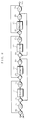
Images


Classifications
-
- H—ELECTRICITY
- H04—ELECTRIC COMMUNICATION TECHNIQUE
- H04L—TRANSMISSION OF DIGITAL INFORMATION, e.g. TELEGRAPHIC COMMUNICATION
- H04L27/00—Modulated-carrier systems
Definitions
- This invention relates to modulators, and more specifically to a modulator for modulating a carrier wave with a transmission signal to be transmitted.
- the first modulator is a device for modulating a carrier wave with a transmission signal to generate a modulated signal, including a quadrature base band generator 71, a quadrature polar coordinate converter 72, a phase accumulator 73, an adder 74, a sine wave table memory 75, a multiplier 76, and a D/A converter 77.
- the quadrature base band generator 71 converts an input digital signal into a quadrature base band signal.
- a modulated signal is represented as the synthesis of two carriers orthogonal to each other, the quadrature base band signal represents amplitude and phase of these carriers.
- the quadrature polar coordinate converter 72 converts the quadrature base band signal into a phase modulating signal and an amplitude modulating signal.
- the phase modulating signal and the amplitude modulating signal represent phase and amplitude of the modulated signal.
- the adder 74 adds the phase modulating signal to an output from the phase accumulator 73.
- the sine wave table memory 75 outputs a carrier signal of a sine wave based on an output from the adder 74.
- the multiplier 76 multiplies the carrier signal by the amplitude modulating signal.
- the first modulator generates a modulated signal with prescribed variations in phase and amplitude.
- FIG. 13 showing its block structure and FIGS. 14a to 14d showing output waveforms from each component.
- the modulator includes a signal point arranging circuit 81, a complex coefficient BPF (Band Pass Filter) 82, a latch 83, a D/A converter 84, and an analog BPF 85, and performs modulation without generating a trigonometric function.
- BPF Bit Pass Filter
- the signal point arranging circuit 81 outputs a quadrature base band signal.
- the quadrature base band signal is a signal sampled at a sampling rate f c /2, and thus has harmonic components of an integral multiple of f c /2, as shown in FIG. 14a.
- the complex coefficient BPF 82 converts the quadrature base band signal into a complex band signal to select a prescribed frequency band. Therefore, as shown in FIG. 14b, in the quadrature base band signal shown in FIG. 14a, only components in the prescribed frequency band are selected.
- the latch circuit 83 and the D/A converter 84 multiply a real signal component of the complex band signal by a pulse whose duty ratio is smaller than 1 to perform pulse amplitude modulation.
- the analog band pass filter 85 extracts a desired harmonic component in the output from the D/A converter 84.
- the output signal from the D/A converter 84 causes aliasing components of the signal shown in FIG. 14b folded at f s , an operating frequency of the complex coefficient BPF 82, as shown in Fig. 14c.
- the analog BPF 85 extracts only a prescribed harmonic component in the output signals from the D/A converter 84 to generate a modulated signal as shown in FIG. 14d.
- the first modulator has one trigonometric function generating portion composed of the phase accumulator 73 and the sine wave table memory 75.
- the trigonometric function generating portion operates with a clock at least more than double the frequency of the above carrier signal (the center frequency of the modulating signal). That is, it is necessary for the first modulator to operate the trigonometric function generating portion, which is a complicated circuit, with a frequency at least more than double the modulating wave frequency, disadvantageously resulting in increases in a circuit size and power consumption.
- the second modulator Like the second modulator, it is possible to construct a modulator without using a trigonometric function generating portion. However, in this case, since an analog band pass filter is required, it is not suitable for integration of a circuit. Further, in the second modulator, the center frequency of the modulating signal is limited to an integer multiple of fc/2, it can not be disadvantageously changed easily.
- an object of the present invention is to provide a modulator allowing a small circuit size and low power consumption, capable of simply varying a center frequency of a modulating signal and further suitable for integration.
- a first aspect of the present invention is a device for modulating a carrier wave with a transmission signal to be transmitted, including:
- the band pass portion since the band pass portion operates at the second sampling rate, inputting a discrete signal sampled at the first sampling rate is the same as inputting a discrete signal obtained by sampling the first discrete signal at the second sampling rate.
- the band pass portion executes band selection with respect to the discrete signal, selecting only a signal which exists in a prescribed frequency band as a modulated signal (a signal obtained by modulating a carrier with the transmission signal to be transmitted).
- the band pass portion operates at the second sampling rate and simply executes band selecting operation.
- the trigonometric function generating portion of the conventional modulator operates at the second sampling rate.
- the structure of the trigonometric function generating portion is complicated.
- power consumption of the band pass portion is small compared with that of the trigonometric function generating portion.
- the discrete signal generating portion preceding to the band pass portion operates at the first sampling rate which is relatively low, it is possible to make power consumption low.
- the first aspect unlike the conventional modulator, it is possible to generate a modulating signal without using the trigonometric function generating portion whose circuit structure is complicated.
- the discrete signal generating portion is composed of a low pass filter for operating at the first sampling rate when the transmission signal is inputted from outside and passing only a signal which exists in low frequencies.
- the discrete signal generating portion generates a discrete signal using only a low pass filter which operates at the first sampling rate. Therefore, in accordance with the second aspect, it is possible to make the circuit size small and power consumption low in the modulator.
- the transmission signal is previously band-limited, and the discrete signal generating portion is composed of an interpolating filter for, when the transmission signal is inputted from outside, interpolating the transmission signal at the first sampling rate.
- the discrete signal generating portion generates a discrete signal using only an interpolating filter for interpolating the transmission signal at the first sampling rate. Therefore, in accordance with the third aspect, it is possible to make the circuit size small and power consumption low in the modulator.
- the transmission signal is previously band-limited and sampled at the first sampling rate
- the discrete signal generating portion includes a trigonometric function generating portion for generating a trigonometric function with a prescribed frequency, and a multiplying portion for, when the transmission signal is inputted from outside, multiplying the transmission signal by the trigonometric function generated in the trigonometric function generating portion.
- the discrete signal generating portion since the discrete signal generating portion includes a trigonometric function generating portion and a multiplying portion, it is possible to freely shift the center frequency of the discrete signal. Thus, it is possible to arbitrarily set the center frequency of the modulating signal.
- the trigonometric function generating portion and the multiplying portion are structural components of the discrete signal generating portion and thus operate at the first sampling rate which is relatively low, also allowing low power consumption .
- the discrete signal generating portion includes a low pass filter for, when the transmission signal is inputted from outside, passing only a signal which exists in low frequencies, and an interpolating filter for interpolating the transmission signal band-limited by the low pass filter at the first sampling rate.
- the discrete signal generating portion since the discrete signal generating portion includes a low pass filter and an interpolating filter, the transmission signal does not have to be band-limited nor sampled at the first sampling rate. Therefore, this improves usability of the modulator. Further, in the fifth aspect, unlike the conventional modulator, it is possible to generate a modulating signal without using the trigonometric function generating portion whose circuit structure is complicated. Therefore, in accordance with the fifth aspect, it is possible to make the circuit size small and power consumption low compared to the conventional modulator.
- the discrete signal generating portion includes a low pass filter for, when the transmission signal is inputted from outside, operating at the first sampling rate and passing only a signal which exists in low frequencies, a trigonometric function generating portion for generating a trigonometric function with a prescribed frequency, and a multiplying portion for multiplying an output signal from the low pass filter by the trigonometric function generated in the trigonometric function generating portion.
- the discrete signal generating portion since the discrete signal generating portion includes a low pass filter, the transmission signal does not have to be band-limited. Thus, this improves usability of the modulator. Further, in accordance with the sixth aspect, since the discrete signal generating portion includes a trigonometric function generating portion and a multiplying portion, as in the fourth aspect, it is possible to arbitrarily set the center frequency of the modulating signal. Furthermore, these portions operate at a relatively low speed, allowing low power consumption of the modulator.
- the transmission signal is previously band-limited
- the discrete signal generating portion includes an interpolating filter for interpolating the transmission signal inputted from outside and band-limited and then outputting a result at said first sampling rate, a trigonometric function generating portion for generating a trigonometric function with a prescribed frequency, and a multiplying portion for multiplying an output signal from the interpolating filter by the trigonometric function generated in the trigonometric function generating portion.
- the discrete signal generating portion since the discrete signal generating portion includes an interpolating filter, the transmission signal does not have to be sampled at the first sampling rate. Thus, this improves usability of the modulator. Further, in accordance with the seventh aspect, since the discrete signal generating portion includes a trigonometric function generating portion and a multiplying portion, like the fourth aspect, it is possible to arbitrarily set the center frequency of the modulating signal. Furthermore, these portions operate at a relatively low speed, allowing low power consumption of the modulator.
- the discrete signal generating portion includes a low pass filter for, when said transmission signal is inputted from outside, passing only a signal which exists in low frequencies, an interpolating filter for interpolating the output signal from the low pass filter and then outputting a result at the first sampling rate, a trigonometric function generating portion for generating a trigonometric function with a prescribed frequency, and a multiplying portion for multiplying an output signal from the interpolating filter by the trigonometric function generated in the trigonometric function generating portion.
- the discrete signal generating portion since the discrete signal generating portion includes a low pass filter and an interpolating filter, the transmission signal does not have to be band-limited nor sampled at the first sampling rate. Thus, this improves usability of the modulator. Further, in accordance with the eighth aspect, since the discrete signal generating portion includes a trigonometric function generating portion and a multiplying portion, like the fourth aspect, it is possible to arbitrarily set the center frequency of the modulating signal. Furthermore, these portions operate at a relatively low speed, allowing low power consumption of the modulator.
- the band pass portion is composed of an IIR filter, and when the discrete signal generated in the discrete signal generating portion is inputted, the IIR filter operates at the second sampling rate and executes the band selection.
- the band pass portion is composed of an IIR filter, it is possible to reduce the number of taps in the filter compared to an FIR filter in an eleventh aspect described below, and also to make the circuit size small and power consumption low in the modulator.
- the band pass portion is composed of a leapflog IIR filter, and when the discrete signal generated in the discrete signal generating portion is inputted, the leapflog IIR filter operates at the second sampling rate and executes the band selection.
- the band pass portion is composed of a leapflog IIR filter, it is possible to reduce the accuracy of elements composing the filter compared to the IIR filter in the ninth aspect described above, and also to make the circuit size small and power consumption low in the modulator.
- the band pass portion is composed of an FIR filter, and when the discrete signal generated in the discrete signal generating portion is inputted, the FIR filter operates at the second sampling rate and executes the band selection.
- the band pass portion is composed of an FIR filter
- the degree of accuracy of elements composing the filter can be as low as the accuracy to be secured at input/output of the band pass portion.
- the low pass filter has a frequency pass characteristic capable of compensating a frequency pass characteristic which the IIR filter or the FIR filter has.
- the band pass filter is provided with the above described frequency pass characteristic. This improves the quality of the modulated signal.
- the band pass portion multiplies the currently inputted signal by a coefficient stored therein at the time of executing the band selection, and before the band selection operation is executed, the multiplying portion determines the coefficient based on the trigonometric function generated in the trigonometric function generating portion and the coefficient determined in the multiplying portion is stored in the band pass portion.
- the trigonometric function generating portion and the multiplying portion determines the coefficient of the band pass portion.
- the discrete signal generating portion and the band pass portion are both constructed of elements for executing digital signal processing.
- the modulator is suitable for integration.
- FIG. 1 is a block diagram showing the structure of a modulator according to a first embodiment of the present invention.
- the modulator includes a low frequency signal generating portion 1 (corresponding to "discrete signal generating means” in claims) and a band pass portion 2.
- the low frequency signal generating portion 1 samples a signal to be transmitted inputted from outside (hereinafter referred to as "transmission signal”) at a first sampling rate f 1 to generate and output a first discrete signal (corresponding to "discrete signal” in claims).
- FIG. 2a A time waveform of the first discrete signal is shown in FIG. 2a, and a spectrum of the first discrete signal is shown in FIG. 3a.
- the transmission signal shown by a dotted line in the drawing is sampled as described above, and thus the first discrete signal is composed of a signal series shown by ⁇ marks in the drawing.
- a center of the spectrum of the first discrete signal is at a prescribed frequency (now assume "0").
- FIG. 3a only the spectrum within a frequency band of ⁇ f 1 /2 is shown in FIG. 3a.
- the band pass portion 2 When the first discrete signal is inputted from the low frequency signal generating portion 1, the band pass portion 2 operates at a second sampling rate f 2 (f 2 >f 1 ) to execute band selection which will be described later. At this time, the band pass portion 2 operates at f 2 , resulting in, substantially, sampling the first discrete signal at f 2 to generate a second discrete signal.
- FIG. 2b A time waveform of the second discrete signal is shown in FIG. 2b, and a spectrum of the second discrete signal is shown in FIG. 3b.
- FIG. 2b when the first discrete signal is sampled at f 2 , since f 2 >f 1 , there are points where no first discrete signal exists. At this point, 0 occurs to form a signal series (refer to ⁇ in the drawing).
- a signal series corresponding to the amplitude of the first discrete signal occurs. Therefore, the waveform of the second discrete signal is composed of a signal series shown by ⁇ and ⁇ in the drawing. Further, in FIG.
- the spectrum of the second discrete signal exists at a position obtained by frequency-shifting the spectrum of the first discrete signal (refer to FIG. 3a) by an integral multiple of the frequency f 1 .
- the spectrum which exists within a frequency band between -f 2 /2 and +f 2 /2 are shown in FIG. 3b.
- the band pass portion 2 selects only components which exist within a prescribed frequency band in the spectrum of the second discrete signal to output a modulated signal.
- the modulated signal has a spectrum as shown in FIG. 3c.
- the modulated signal is a signal obtained by modulating a carrier wave of a frequency 3f 1 using a transmission signal.
- a center frequency of the modulated signal to be outputted from the modulator is f c
- its occupied frequency bandwidth is ⁇ B having its center at f c .
- at least 2(f c +B) must be selected as f 2 according to a sampling theorem.
- f 2 /n is selected as f 1 by dividing f 2 by an integer n.
- f 1 >2B is required to prevent interference from an adjacent spectrum.
- the center of the spectrum of the second discrete signal obtained by sampling the first discrete signal at f 2 appears at positions, as shown in FIG. 4b, obtained by an integral multiple of f 1 based on the center frequency of the first discrete signal. That is, when k is assumed as an appropriate integer, f c /k is selected as f 1 .
- the center of the spectrum of the second discrete signal obtained by sampling the first discrete signal at f 2 appears at positions, as shown in FIG. 5b, obtained by an integral multiple of f 1 based on the center frequency of the first discrete signal. That is, the center of the spectrum of the second discrete signal appears at each f 1 , allowing being arbitrarily shifted in the frequency bandwidth of f 1 . Therefore, when the spectrum of the first discrete signal has a center at an arbitrary frequency, it is possible to independently set f 1 and f c .
- the low frequency signal generating portion 1 includes a low pass filter 51, an interpolating filter 52, and a frequency converting portion 53. Furthermore, the frequency converting portion 53 has a multiplying portion 55 and a trigonometric function generating portion 54 (refer to a portion surrounded by a dotted line in FIG. 6).
- the low pass filter 51 executes root roll off filtering and the like with respect to a symbol value of a transmission signal inputted from outside, and then outputs a band-limited signal obtained by sampling the symbol value after filtering at a sampling rate f L .
- this low pass filter 51 is not required.
- the interpolating filter 52 executes filtering to pass a low frequency portion at a sampling rate f 1 with respect to the band-limited signal inputted from the low pass filter 51 or outside, thereby interpolating the inputted band-limited signal at the first sampling rate f 1 . That is, the interpolating filter 52 converts the sampling rate of the band-limited signal from f L to f 1 .
- An output signal from the interpolating filter 52 has the same spectrum as that shown in FIG. 3a.
- a rate obtained by dividing f 1 by an arbitrary integer is used as f L . That is, f L ⁇ f 1 .
- the trigonometric function generating portion 54 included in the frequency converting portion 53 generates a trigonometric function with a prescribed frequency. As describe above, there are cases where the first discrete signal has an arbitrary center frequency other than 0 (refer to FIG. 5a). The frequency of the above trigonometric function defines its center frequency.
- the multiplying portion 55 included in the frequency converting portion 53 multiplies the output signal of the interpolating filter 52 by the trigonometric function outputted from the trigonometric function generating portion 54 to shift the center frequency of the output signal.
- the trigonometric function generating portion 54 and the multiplying portion 55 operate at f 1 which is lower than f 2 of the final sampling rate.
- the first modulator (refer to FIG. 12) to operate the phase accumulator 73 and the sine wave table memory 75, which correspond to the trigonometric function generating portion, at a clock rate which satisfies f 2 ⁇ 2(f c +B).
- the trigonometric function generating portion 54 and the multiplying portion 55 of the present modulator can make the circuit size small and power consumption low compared to the first modulator.
- the frequency converting portion 53 is required only when generating the first discrete signal as shown in FIG. 5a, and not required when generating the first discrete signal whose center frequency is "0" (refer to FIG. 3a).
- multiplying portion 55 has been described assuming that the output signal from the interpolating filter 52 is inputted thereto, there are cases, as is evident from the above, where the transmission signal is directly inputted from outside or the output signal from the low pass filter 51 is inputted.
- the band pass portion 2 Described next is an example of structure of the band pass portion 2.
- the spectrum of the modulated signal generated by the present modulator is symmetrical as shown in FIG. 3c like an amplitude modulating signal and a BPSK (Binary Phase Shift Keying) modulating signal and the spectrum of the first discrete signal has a center at a frequency 0, the first discrete signal becomes a real signal. Therefore, as the band pass portion 2, a filter with real coefficients is used.
- the first discrete signal becomes a complex signal. Therefore, for the band pass portion 2, a filter with complex coefficients has to be used. However, since the frequency components to be selected by the band pass portion 2 are more than 0 and less than f 2 /2, it is enough to output from the band pass portion 2 either of the real components or imaginary components among outputs from the complex coefficient filter.
- the band pass portion 2 can be realized by using an IIR (Infinite Impulse Response) filer as shown in FIG. 7.
- the IIR filter includes multipliers 11 0 to 11 N for multiplying each input by coefficients b 0 to b N , multipliers 12 1 to 12 N for multiplying each feedback value of output by coefficients a 1 to a N , adders 13 0 to 13 N for adding a plurality of input values, and delay elements 14 1 to 14 N for giving delay T to the input values.
- the adder 13 N outputs a value obtained by adding two multiplied values inputted from the multiplier 11 N and the multiplier 12 N to the delay element 14 N .
- the adders 13 (N-1) to 13 1 adds two multiplied values inputted from the multipliers 11 (N-1) to 11 1 and the multipliers 12 (N-1) to 12 1 and values inputted from the delay elements 14 n to 14 2 to output the result to the delay elements 14 (N-1) to 14 1 .
- the adder 13 0 adds the multiplied value inputted from the multiplier 11 0 and a value inputted from the delay element 14 1 , and thus an output of the IIR filter can be obtained. Further, since the IIR filter performs the above operation at the second sampling rate f 2 , when the first discrete signal is inputted, the IIR filter selects only components which exist within a prescribed frequency band in the spectrum included in the second discrete signal (refer to FIG. 3b and FIG. 5b) to generate a modulated signal.
- the leapflog filter includes multipliers 15 0 to 15 5 , subtracters 16 1 to 16 5 , and integrators 17 1 to 17 4 .
- the integrators 17 1 to 17 4 hold one state variable each.
- the integrators 17 1 to 17 4 have, as shown in FIG. 9, adders 18 1 to 18 4 , delay elements 19 1 to 19 4 , and multipliers 20 1 to 20 4 , respectively.
- the adders 18 1 to 18 4 add an input value and a feedbacked output value (output from the multipliers 20 1 to 20 4 ).
- the delay elements 19 1 to 19 4 give a delay value T to the output value from the adders 18 1 to 18 4 .
- the multipliers 20 1 to 20 4 multiply the output value from the delay elements 19 1 to 19 4 by a coefficient e 1 and then output the results.
- FIG. 8 is now referred again.
- a coefficient r of the multiplier 15 0 and a coefficient y of the multiplier 15 5 correspond to output step resistance and input step resistance when the filter is formed of an analog filter.
- coefficients k 1 and k 3 of the multipliers 15 1 and 15 3 correspond to an inductance of the analog filter and coefficients k 2 and k 4 of the multipliers 15 2 and 15 4 correspond to a capacitance of the analog filter.
- the filter operates by feedbacking outputs from the multipliers 15 0 to 15 4 to the subtracter 16 1 to 16 4 .
- the leapflog filter as the band pass portion 2 selects components which exist in a prescribed frequency band from the spectrum included in the second discrete signal (refer to FIG. 3b and FIG. 5b) generated simply by input of the first discrete signal to generate a modulated signal.
- the band pass portion 2 can be realized by using an FIR (Finite Impulse Response) filter as shown in FIG. 10.
- the FIR filter is composed of N taps, including multipliers 21 0 to 21 N for multiplying each input value thereto by coefficients c 0 to c N and outputting the results, multipliers 23 1 to 23 N for giving each input value thereto a delay T and outputting the results, and adders 22 1 to 22 N for adding a plurality of input values and outputting the results.
- FIR Finite Impulse Response
- the multiplier 21 0 multiplies an input value by the coefficient c 0
- the multipliers 21 1 to 21 N multiplies output values from the delay elements 23 1 to 23 N by the coefficients c 1 to c N .
- the delay element 23 i (i is not less than 2) gives the output value of the delay element 23 (i-1) the delay T. Then, the results obtained by multiplying of the multipliers 21 0 to 21 N are synthesized by the adders 22 1 to 22 N to become an output of the FIR filter.
- the FIR filter as the band pass portion 2 selects only the components which exist in a prescribed frequency band in the spectrum of the second discrete signal (refer to FIG. 3b and FIG. 5b) to generate a modulated signal.
- the FIR filter when the FIR filter is applied to the band pass portion 2, a large number of taps N is required.
- the accuracy of the operating elements constructing the FIR filter can be as low as the accuracy to be secured at input/ output of the band pass portion 2, it is possible to operate the modulator at a high speed.
- FIG. 10 shows principles of the FIR filter, and the number of multipliers in a practical circuit can be smaller than that shown in the drawing. That is, the second discrete signal generated in the FIR filter has a signal series in which most of the signals show 0 as shown in FIG. 2b. Then, before being inputted to the multipliers 21 0 to 21 N , the second discrete signal is given delay by the delay element of each preceding step. Therefore, not all of the multipliers 21 simultaneously output the results obtained by multiplying of non-0. Thus, in view of miniaturization of the modulator, it is effective that the FIR filter is constructed so as to include a small number of multipliers 21 and to perform filtering as switching to the multiplier 21 which outputs the result obtained by multiplying of non-0.
- the IIR filter when used for the band pass portion 2, amplitude and phase characteristics of the output signal can be disturbed by the frequency.
- the FIR filter when used, the amplitude characteristic of the output signal can be disturbed by the frequency.
- the low frequency signal generating portion 1 includes the low pass filter 51 (refer to FIG. 6) and the frequency pass characteristic of the filter 51 has a characteristic opposite to the above disturbance, it is possible to eliminate the disturbance in the amplitude and phase characteristics when viewed as the whole modulator.
- the band pass portion 2 can freely vary the center frequency f c only by rewriting each coefficient. Described below are values to be set as coefficients of the IIR and FIR filters.
- an original filter which has the same frequency pass characteristic as that of the filters and whose center frequency is 0 is planned and thereby coefficients of the original filter are obtained.
- the coefficients of the original filter are multiplied by s k shown in the following equation (1) to take the results as the coefficients of the IIR or FIR filter.
- s k cos2 ⁇ kf c /f 2 +jsin2 ⁇ kf c /f 2
- k is a relative integer showing the number of sample delays when the input signal is multiplied by the coefficient. More specifically, for example, when s 0 is used, it is possible to obtain b 0 (refer to FIG. 7) and c 0 (refer to FIG. 10), and when s 1 is used, it is possible to obtain a 1 and b 1 (refer to FIG. 7), and c 1 (refer to FIG. 10). Other coefficients can be obtained in the same manner.
- f c is a center frequency of the modulating signal
- f 2 is the second sampling rate
- j is the imaginary unit.
- the processing is the same as frequency conversion processing by the frequency converting portion 53.
- the frequency conversion portion 53 can be used as a circuit for rewriting the coefficients of the IIR or FIR filter constructing the band pass portion 2. Described below is a modulator with such structure as a second embodiment referring FIG. 11 showing its block structure.
- the modulator is different in that the modulator further includes a coefficient generating portion 61, compared to the modulator shown in FIG. 1. Since the general structure except the above is the same as that shown in FIG.1, corresponding structural parts are given the same reference numerals and their description is omitted. Further, in FIG. 11, the low frequency signal generating portion 1 is different only in that it further includes switches 62 and 63, compared to the low frequency signal generating portion 1 shown in FIG. 6, and thus other corresponding structural parts are given the same reference numerals and their description is omitted.
- the coefficient generating portion 61 stores the coefficients of the original filter obtained as described above.
- a terminal (a) included in the switch 62 is connected to the interpolating filter 52, a terminal (b) included in the switch 62 is connected to the coefficient generating portion 61, and the interpolating filter 52 or the coefficient generating portion 61 is connected to the frequency converting portion 53 by switching.
- a terminal (a) included in the switch 63 is connected to a signal input terminal of the band pass portion 2
- a terminal (b) included in the switch 63 is connected to a coefficient input terminal of the band pass portion 2
- the signal input terminal or the coefficient input terminal is connected to the frequency converting portion 53 by switching.
- both of the switches 62 and 63 select the terminal (a) to connect the interpolating filter 52 and the frequency converting portion 53.
- the operation of the modulator is evident from the first embodiment, and thus its description is omitted.
- both of the switches 62 and 63 select the terminal (b) to connect the coefficient generating portion 61 and the frequency converting portion 53. Then, the coefficient of the original filter outputted from the coefficient generating portion 61 is outputted to the multiplying portion 55.
- a trigonometric function is inputted from the trigonometric function generating portion 54, and the multiplying portion 55 multiplies the coefficient of the original filter by the trigonometric function to generate and output a coefficient of the IIR or FIR filter included in the band pass portion 2.
- the coefficients generated in the above manner are outputted to the band pass portion 2 and set in a register storing the coefficients of the IIR or FIR filter, and the like.
- the multiplying portion 55 calculates the coefficients of the IIR or FIR filter.
- the modulator it is not required to use the trigonometric function generating portion, or if the trigonometric function generating portion is used, its operating rate is low, allowing a small circuit size and low power consumption.
- the center frequency of the modulating signal can be varied by changing the coefficients of the filter (IIR or FIR) constructing the band pass portion as required.
- the modulator is convenient for integration if structural parts are each constructed by digital elements, they may be constructed by analog elements.
Abstract
Description
Claims (20)
- A device for modulating a carrier with a transmission signal to be transmitted, including:discrete signal generating means for sampling said transmission signal inputted from outside at a first sampling rate and generating a discrete signal; andband pass means for operating at a second sampling rate higher than said first sampling rate when the discrete signal generated in said discrete signal generating means is inputted and executing band selection for selecting a signal which exists in a prescribed frequency band.
- The modulator according to claim 1, whereinsaid discrete signal generating means is composed ofa low pass filter for operating at said first sampling rate when said transmission signal is inputted from outside and passing only a signal which exists in low frequencies.
- The modulator according to claim 1, whereinsaid transmission signal is previously band-limited, andsaid discrete signal generating means comprisesan interpolating filter for, when said transmission signal is inputted from outside, interpolating the transmission signal at said first sampling rate.
- The modulator according to claim 1, whereinsaid transmission signal is previously band-limited and sampled at the first sampling rate, andsaid discrete signal generating means includestrigonometric function generating means for generating a trigonometric function with a prescribed frequency, andmultiplying means for, when said transmission signal is inputted from outside, multiplying the transmission signal by the trigonometric function generated in said trigonometric function generating means.
- The modulator according to claim 1, whereinsaid discrete signal generating means includesa low pass filter for, when said transmission signal is inputted from outside, passing only a signal which exists in low frequencies, andan interpolating filter for interpolating the transmission signal band-limited by said low pass filter at said first sampling rate.
- The modulator according to claim 1, whereinsaid discrete signal generating means includesa low pass filter for, when said transmission signal is inputted from outside, operating at the first sampling rate and passing only a signal which exists in low frequencies,trigonometric function generating means for generating a trigonometric function with a prescribed frequency, andmultiplying means for multiplying an output signal from said low pass filter by the trigonometric function generated in said trigonometric function generating means.
- The modulator according to claim 1, whereinsaid transmission signal is previously band-limited, andsaid discrete signal generating means includesan interpolating filter for interpolating the transmission signal inputted from outside and band-limited and outputting a result at said first sampling rate,trigonometric function generating means for generating a trigonometric function with a prescribed frequency and outputting the result, andmultiplying means for multiplying an output signal from said interpolating filter by the trigonometric function generated in said trigonometric function generating means.
- The modulator according to claim 1, whereinsaid discrete signal generating means includesa low pass filter for, when said transmission signal is inputted from outside, passing only a signal which exists in low frequencies,an interpolating filter for interpolating the output signal from said low pass filter and then outputting the result at said first sampling rate,trigonometric function generating means for generating a trigonometric function with a prescribed frequency, andmultiplying means for multiplying an output signal from said interpolating filter by the trigonometric function generated in said trigonometric function generating means.
- The modulator according to claim 1, whereinsaid band pass means is composed of an IIR filter, andwhen the discrete signal generated in said discrete signal generating means is inputted, said IIR filter operates at said second sampling rate and executes said band selection.
- The modulator according to claim 1, whereinsaid band pass means is composed of a leapflog IIR filter, andwhen the discrete signal generated in said discrete signal generating means is inputted, said leapflog IIR filter operates at said second sampling rate and executes said band selection.
- The modulator according to claim 1, whereinsaid band pass means is composed of an FIR filter, andwhen the discrete signal generated in said discrete signal generating means is inputted, said FIR filter operates at said second sampling rate and executes said band selection.
- The modulator according to claim 2, whereinwhen said band pass means includes an IIR filter or an FIR filter,said low pass filter has a frequency pass characteristic capable of compensating a frequency pass characteristic which said IIR filter or said FIR filter has.
- The modulator according to claim 5, whereinwhen said band pass means includes an IIR filter or an FIR filter,said low pass filter has a frequency pass characteristic capable of compensating a frequency pass characteristic which said IIR filter or said FIR filter has.
- The modulator according to claim 6, whereinwhen said band pass means includes an IIR filter or an FIR filter,said low pass filter has a frequency pass characteristic capable of compensating a frequency pass characteristic which said IIR filter or said FIR filter has.
- The modulator according to claim 8, whereinwhen the band pass means includes an IIR filter or an FIR filter, said low pass filter has a frequency pass characteristic capable of compensating a frequency pass characteristic which said SIR filter or said FIR filter has.
- The modulator according to claim 4, whereinsaid band pass means multiplies the currently inputted signal by a coefficient stored therein at the time of executing said band selection, andbefore said band selection operation is executed, said multiplying means determines said coefficient based on the trigonometric function generated in said trigonometric function generating means andthe coefficient determined in said multiplying means is stored in said band pass means.
- The modulator according to claim 6, whereinsaid band pass means multiplies the currently inputted signal by a coefficient stored therein at the time of executing said band selection, andbefore said band selection operation is executed, said multiplying means determines said coefficient based on the trigonometric function generated in said trigonometric function generating means andthe coefficient determined in said multiplying means is stored in said band pass means.
- The modulator according to claim 7, whereinsaid band pass means multiplies the currently inputted signal by a coefficient stored therein at the time of executing said band selection, andbefore said band selection operation is executed, said multiplying means determines said coefficient based on the trigonometric function generated in said trigonometric function generating means andthe coefficient determined in said multiplying means is stored in said band pass means.
- The modulator according to claim 8, whereinsaid band pass means multiplies the currently inputted signal by a coefficient stored therein at the time of executing said band selection, andbefore said band selection operation is executed, said multiplying means determines said coefficient based on the trigonometric function generated in said trigonometric function generating means andthe coefficient determined in said multiplying means is stored in said band pass means.
- The modulator according to claim 1, whereinsaid discrete signal generating means and said band pass means are both constructed of elements for executing digital signal processing.
Applications Claiming Priority (3)
| Application Number | Priority Date | Filing Date | Title |
|---|---|---|---|
| JP9198919A JPH1141305A (en) | 1997-07-24 | 1997-07-24 | Modulating device |
| JP19891997 | 1997-07-24 | ||
| JP198919/97 | 1997-07-24 |
Publications (2)
| Publication Number | Publication Date |
|---|---|
| EP0893900A2 true EP0893900A2 (en) | 1999-01-27 |
| EP0893900A3 EP0893900A3 (en) | 2002-02-06 |
Family
ID=16399150
Family Applications (1)
| Application Number | Title | Priority Date | Filing Date |
|---|---|---|---|
| EP98113817A Withdrawn EP0893900A3 (en) | 1997-07-24 | 1998-07-23 | Modulator |
Country Status (4)
| Country | Link |
|---|---|
| US (1) | US6184756B1 (en) |
| EP (1) | EP0893900A3 (en) |
| JP (1) | JPH1141305A (en) |
| CN (1) | CN1207621A (en) |
Families Citing this family (6)
| Publication number | Priority date | Publication date | Assignee | Title |
|---|---|---|---|---|
| PL351813A1 (en) * | 2000-01-07 | 2003-06-16 | Koninkl Philips Electronics Nv | Method of deriving the coefficients to be use in an encoding device prediction filter |
| GB2359950B (en) * | 2000-02-29 | 2004-06-30 | Ericsson Telefon Ab L M | Signal filtering |
| JP5274014B2 (en) * | 2004-10-13 | 2013-08-28 | メディアテック インコーポレーテッド | Communication system filter |
| US7242326B1 (en) * | 2005-12-23 | 2007-07-10 | Cirrus Logic, Inc. | Sample rate conversion combined with filter |
| US7342525B2 (en) * | 2005-12-23 | 2008-03-11 | Cirrus Logic, Inc. | Sample rate conversion combined with DSM |
| EP3157112A1 (en) * | 2015-10-12 | 2017-04-19 | General Electric Technology GmbH | Improvements in or relating to the protection of power transformers |
Citations (4)
| Publication number | Priority date | Publication date | Assignee | Title |
|---|---|---|---|---|
| US4003002A (en) * | 1974-09-12 | 1977-01-11 | U.S. Philips Corporation | Modulation and filtering device |
| DE4041632A1 (en) * | 1990-03-15 | 1992-07-02 | Ant Nachrichtentech | Preparing several TV signals for transmission - involves frequency conversion and multiplexing with additional digital filter preceding channel bandpass filter with same clock rate |
| FR2689350A1 (en) * | 1992-03-30 | 1993-10-01 | France Telecom | Residual sideband amplitude modulator for sampled analogue or digital signals for television - has sampling circuit with over-sampling ratio of 2 or more, low pass filter, modulator, Nyquist filter and D=A converter |
| EP0651526A2 (en) * | 1993-10-30 | 1995-05-03 | Robert Bosch Gmbh | Method for processing a digital frequencymultiplex signal |
Family Cites Families (5)
| Publication number | Priority date | Publication date | Assignee | Title |
|---|---|---|---|---|
| US5420887A (en) | 1992-03-26 | 1995-05-30 | Pacific Communication Sciences | Programmable digital modulator and methods of modulating digital data |
| JPH06152675A (en) | 1992-11-05 | 1994-05-31 | N T T Idou Tsuushinmou Kk | Digital modulator |
| JP3400003B2 (en) | 1993-02-18 | 2003-04-28 | 株式会社日立製作所 | Complex modulation and demodulation method |
| US5519732A (en) * | 1994-05-02 | 1996-05-21 | Harris Corporation | Digital baseband to IF conversion in cellular base stations |
| US5783974A (en) * | 1997-01-27 | 1998-07-21 | Hitachi America, Ltd. | Digital interpolation up sampling circuit and digital modulator using same |
-
1997
- 1997-07-24 JP JP9198919A patent/JPH1141305A/en active Pending
-
1998
- 1998-07-21 US US09/119,644 patent/US6184756B1/en not_active Expired - Lifetime
- 1998-07-23 EP EP98113817A patent/EP0893900A3/en not_active Withdrawn
- 1998-07-24 CN CN98116396A patent/CN1207621A/en active Pending
Patent Citations (4)
| Publication number | Priority date | Publication date | Assignee | Title |
|---|---|---|---|---|
| US4003002A (en) * | 1974-09-12 | 1977-01-11 | U.S. Philips Corporation | Modulation and filtering device |
| DE4041632A1 (en) * | 1990-03-15 | 1992-07-02 | Ant Nachrichtentech | Preparing several TV signals for transmission - involves frequency conversion and multiplexing with additional digital filter preceding channel bandpass filter with same clock rate |
| FR2689350A1 (en) * | 1992-03-30 | 1993-10-01 | France Telecom | Residual sideband amplitude modulator for sampled analogue or digital signals for television - has sampling circuit with over-sampling ratio of 2 or more, low pass filter, modulator, Nyquist filter and D=A converter |
| EP0651526A2 (en) * | 1993-10-30 | 1995-05-03 | Robert Bosch Gmbh | Method for processing a digital frequencymultiplex signal |
Also Published As
| Publication number | Publication date |
|---|---|
| CN1207621A (en) | 1999-02-10 |
| EP0893900A3 (en) | 2002-02-06 |
| JPH1141305A (en) | 1999-02-12 |
| US6184756B1 (en) | 2001-02-06 |
Similar Documents
| Publication | Publication Date | Title |
|---|---|---|
| JP2926615B2 (en) | SSB signal generator | |
| KR100484710B1 (en) | Resampling Circuit and Control Method | |
| US5473280A (en) | Modulation/demodulation method and system for realizing quadrature modulation/demodulation technique used in digital mobile radio system with complex signal processing | |
| KR100446540B1 (en) | Transmitter for a data communication | |
| US4812786A (en) | Method and system for providing precise multi-function modulation | |
| US4015222A (en) | Modulated passband signal generator | |
| JPS6255325B2 (en) | ||
| EP0893900A2 (en) | Modulator | |
| JP3323124B2 (en) | Modulation method and device | |
| JP4376222B2 (en) | Wave shaping digital filter circuit | |
| US7164713B2 (en) | Interpolating root nyquist filter for variable rate modulator | |
| JPH06291790A (en) | Pi/4 shift qpsk modulator | |
| JP2000036846A (en) | Digital modulator | |
| EP0576215A1 (en) | Rate converter for converting data rate | |
| JP3441255B2 (en) | Signal generation device and transmission device using the same | |
| JP3864034B2 (en) | Wave shaping digital filter circuit | |
| JP3842396B2 (en) | Digital modulator | |
| JPH0640616B2 (en) | Digital filter-frequency characteristic converter | |
| JPH06104943A (en) | Four-phase modulator | |
| JPH06152675A (en) | Digital modulator | |
| JP4790145B2 (en) | Digital up converter | |
| KR0154087B1 (en) | Cpm signal generator | |
| Ke et al. | The design of baseband signal generator | |
| JP3802772B2 (en) | Orthogonal frequency division multiplex modulation circuit | |
| JP3893197B2 (en) | Digital modulation circuit |
Legal Events
| Date | Code | Title | Description |
|---|---|---|---|
| PUAI | Public reference made under article 153(3) epc to a published international application that has entered the european phase |
Free format text: ORIGINAL CODE: 0009012 |
|
| AK | Designated contracting states |
Kind code of ref document: A2 Designated state(s): AT BE CH CY DE DK ES FI FR GB GR IE IT LI LU MC NL PT SE Kind code of ref document: A2 Designated state(s): DE ES FR GB IT |
|
| AX | Request for extension of the european patent |
Free format text: AL;LT;LV;MK;RO;SI |
|
| PUAL | Search report despatched |
Free format text: ORIGINAL CODE: 0009013 |
|
| AK | Designated contracting states |
Kind code of ref document: A3 Designated state(s): AT BE CH CY DE DK ES FI FR GB GR IE IT LI LU MC NL PT SE |
|
| AX | Request for extension of the european patent |
Free format text: AL;LT;LV;MK;RO;SI |
|
| 17P | Request for examination filed |
Effective date: 20020730 |
|
| AKX | Designation fees paid |
Free format text: DE ES FR GB IT |
|
| 17Q | First examination report despatched |
Effective date: 20070531 |
|
| STAA | Information on the status of an ep patent application or granted ep patent |
Free format text: STATUS: THE APPLICATION IS DEEMED TO BE WITHDRAWN |
|
| 18D | Application deemed to be withdrawn |
Effective date: 20071011 |