EP0903733A2 - Optical recording medium and dipyrromethene metal chelate compound for use therein - Google Patents
Optical recording medium and dipyrromethene metal chelate compound for use therein Download PDFInfo
- Publication number
- EP0903733A2 EP0903733A2 EP98117641A EP98117641A EP0903733A2 EP 0903733 A2 EP0903733 A2 EP 0903733A2 EP 98117641 A EP98117641 A EP 98117641A EP 98117641 A EP98117641 A EP 98117641A EP 0903733 A2 EP0903733 A2 EP 0903733A2
- Authority
- EP
- European Patent Office
- Prior art keywords
- group
- recording medium
- optical recording
- substituted
- carbon atoms
- Prior art date
- Legal status (The legal status is an assumption and is not a legal conclusion. Google has not performed a legal analysis and makes no representation as to the accuracy of the status listed.)
- Granted
Links
Images

Classifications
-
- G—PHYSICS
- G11—INFORMATION STORAGE
- G11B—INFORMATION STORAGE BASED ON RELATIVE MOVEMENT BETWEEN RECORD CARRIER AND TRANSDUCER
- G11B7/00—Recording or reproducing by optical means, e.g. recording using a thermal beam of optical radiation by modifying optical properties or the physical structure, reproducing using an optical beam at lower power by sensing optical properties; Record carriers therefor
- G11B7/24—Record carriers characterised by shape, structure or physical properties, or by the selection of the material
- G11B7/2403—Layers; Shape, structure or physical properties thereof
- G11B7/24035—Recording layers
-
- G—PHYSICS
- G11—INFORMATION STORAGE
- G11B—INFORMATION STORAGE BASED ON RELATIVE MOVEMENT BETWEEN RECORD CARRIER AND TRANSDUCER
- G11B7/00—Recording or reproducing by optical means, e.g. recording using a thermal beam of optical radiation by modifying optical properties or the physical structure, reproducing using an optical beam at lower power by sensing optical properties; Record carriers therefor
- G11B7/24—Record carriers characterised by shape, structure or physical properties, or by the selection of the material
- G11B7/241—Record carriers characterised by shape, structure or physical properties, or by the selection of the material characterised by the selection of the material
- G11B7/242—Record carriers characterised by shape, structure or physical properties, or by the selection of the material characterised by the selection of the material of recording layers
- G11B7/244—Record carriers characterised by shape, structure or physical properties, or by the selection of the material characterised by the selection of the material of recording layers comprising organic materials only
- G11B7/246—Record carriers characterised by shape, structure or physical properties, or by the selection of the material characterised by the selection of the material of recording layers comprising organic materials only containing dyes
-
- G—PHYSICS
- G11—INFORMATION STORAGE
- G11B—INFORMATION STORAGE BASED ON RELATIVE MOVEMENT BETWEEN RECORD CARRIER AND TRANSDUCER
- G11B7/00—Recording or reproducing by optical means, e.g. recording using a thermal beam of optical radiation by modifying optical properties or the physical structure, reproducing using an optical beam at lower power by sensing optical properties; Record carriers therefor
- G11B7/12—Heads, e.g. forming of the optical beam spot or modulation of the optical beam
- G11B7/135—Means for guiding the beam from the source to the record carrier or from the record carrier to the detector
- G11B7/1365—Separate or integrated refractive elements, e.g. wave plates
-
- G—PHYSICS
- G11—INFORMATION STORAGE
- G11B—INFORMATION STORAGE BASED ON RELATIVE MOVEMENT BETWEEN RECORD CARRIER AND TRANSDUCER
- G11B7/00—Recording or reproducing by optical means, e.g. recording using a thermal beam of optical radiation by modifying optical properties or the physical structure, reproducing using an optical beam at lower power by sensing optical properties; Record carriers therefor
- G11B7/24—Record carriers characterised by shape, structure or physical properties, or by the selection of the material
- G11B7/241—Record carriers characterised by shape, structure or physical properties, or by the selection of the material characterised by the selection of the material
- G11B7/242—Record carriers characterised by shape, structure or physical properties, or by the selection of the material characterised by the selection of the material of recording layers
- G11B7/244—Record carriers characterised by shape, structure or physical properties, or by the selection of the material characterised by the selection of the material of recording layers comprising organic materials only
- G11B7/249—Record carriers characterised by shape, structure or physical properties, or by the selection of the material characterised by the selection of the material of recording layers comprising organic materials only containing organometallic compounds
- G11B7/2492—Record carriers characterised by shape, structure or physical properties, or by the selection of the material characterised by the selection of the material of recording layers comprising organic materials only containing organometallic compounds neutral compounds
-
- G—PHYSICS
- G11—INFORMATION STORAGE
- G11B—INFORMATION STORAGE BASED ON RELATIVE MOVEMENT BETWEEN RECORD CARRIER AND TRANSDUCER
- G11B7/00—Recording or reproducing by optical means, e.g. recording using a thermal beam of optical radiation by modifying optical properties or the physical structure, reproducing using an optical beam at lower power by sensing optical properties; Record carriers therefor
- G11B7/24—Record carriers characterised by shape, structure or physical properties, or by the selection of the material
- G11B7/241—Record carriers characterised by shape, structure or physical properties, or by the selection of the material characterised by the selection of the material
- G11B7/242—Record carriers characterised by shape, structure or physical properties, or by the selection of the material characterised by the selection of the material of recording layers
- G11B7/243—Record carriers characterised by shape, structure or physical properties, or by the selection of the material characterised by the selection of the material of recording layers comprising inorganic materials only, e.g. ablative layers
- G11B2007/24302—Metals or metalloids
-
- G—PHYSICS
- G11—INFORMATION STORAGE
- G11B—INFORMATION STORAGE BASED ON RELATIVE MOVEMENT BETWEEN RECORD CARRIER AND TRANSDUCER
- G11B7/00—Recording or reproducing by optical means, e.g. recording using a thermal beam of optical radiation by modifying optical properties or the physical structure, reproducing using an optical beam at lower power by sensing optical properties; Record carriers therefor
- G11B7/24—Record carriers characterised by shape, structure or physical properties, or by the selection of the material
- G11B7/241—Record carriers characterised by shape, structure or physical properties, or by the selection of the material characterised by the selection of the material
- G11B7/242—Record carriers characterised by shape, structure or physical properties, or by the selection of the material characterised by the selection of the material of recording layers
- G11B7/243—Record carriers characterised by shape, structure or physical properties, or by the selection of the material characterised by the selection of the material of recording layers comprising inorganic materials only, e.g. ablative layers
- G11B2007/24318—Non-metallic elements
- G11B2007/24326—Halides (F, CI, Br...)
-
- G—PHYSICS
- G11—INFORMATION STORAGE
- G11B—INFORMATION STORAGE BASED ON RELATIVE MOVEMENT BETWEEN RECORD CARRIER AND TRANSDUCER
- G11B7/00—Recording or reproducing by optical means, e.g. recording using a thermal beam of optical radiation by modifying optical properties or the physical structure, reproducing using an optical beam at lower power by sensing optical properties; Record carriers therefor
- G11B7/24—Record carriers characterised by shape, structure or physical properties, or by the selection of the material
- G11B7/241—Record carriers characterised by shape, structure or physical properties, or by the selection of the material characterised by the selection of the material
- G11B7/242—Record carriers characterised by shape, structure or physical properties, or by the selection of the material characterised by the selection of the material of recording layers
- G11B7/244—Record carriers characterised by shape, structure or physical properties, or by the selection of the material characterised by the selection of the material of recording layers comprising organic materials only
- G11B7/246—Record carriers characterised by shape, structure or physical properties, or by the selection of the material characterised by the selection of the material of recording layers comprising organic materials only containing dyes
- G11B7/247—Record carriers characterised by shape, structure or physical properties, or by the selection of the material characterised by the selection of the material of recording layers comprising organic materials only containing dyes methine or polymethine dyes
- G11B7/2472—Record carriers characterised by shape, structure or physical properties, or by the selection of the material characterised by the selection of the material of recording layers comprising organic materials only containing dyes methine or polymethine dyes cyanine
-
- G—PHYSICS
- G11—INFORMATION STORAGE
- G11B—INFORMATION STORAGE BASED ON RELATIVE MOVEMENT BETWEEN RECORD CARRIER AND TRANSDUCER
- G11B7/00—Recording or reproducing by optical means, e.g. recording using a thermal beam of optical radiation by modifying optical properties or the physical structure, reproducing using an optical beam at lower power by sensing optical properties; Record carriers therefor
- G11B7/24—Record carriers characterised by shape, structure or physical properties, or by the selection of the material
- G11B7/241—Record carriers characterised by shape, structure or physical properties, or by the selection of the material characterised by the selection of the material
- G11B7/252—Record carriers characterised by shape, structure or physical properties, or by the selection of the material characterised by the selection of the material of layers other than recording layers
- G11B7/253—Record carriers characterised by shape, structure or physical properties, or by the selection of the material characterised by the selection of the material of layers other than recording layers of substrates
- G11B7/2533—Record carriers characterised by shape, structure or physical properties, or by the selection of the material characterised by the selection of the material of layers other than recording layers of substrates comprising resins
- G11B7/2534—Record carriers characterised by shape, structure or physical properties, or by the selection of the material characterised by the selection of the material of layers other than recording layers of substrates comprising resins polycarbonates [PC]
-
- G—PHYSICS
- G11—INFORMATION STORAGE
- G11B—INFORMATION STORAGE BASED ON RELATIVE MOVEMENT BETWEEN RECORD CARRIER AND TRANSDUCER
- G11B7/00—Recording or reproducing by optical means, e.g. recording using a thermal beam of optical radiation by modifying optical properties or the physical structure, reproducing using an optical beam at lower power by sensing optical properties; Record carriers therefor
- G11B7/24—Record carriers characterised by shape, structure or physical properties, or by the selection of the material
- G11B7/241—Record carriers characterised by shape, structure or physical properties, or by the selection of the material characterised by the selection of the material
- G11B7/252—Record carriers characterised by shape, structure or physical properties, or by the selection of the material characterised by the selection of the material of layers other than recording layers
- G11B7/256—Record carriers characterised by shape, structure or physical properties, or by the selection of the material characterised by the selection of the material of layers other than recording layers of layers improving adhesion between layers
-
- G—PHYSICS
- G11—INFORMATION STORAGE
- G11B—INFORMATION STORAGE BASED ON RELATIVE MOVEMENT BETWEEN RECORD CARRIER AND TRANSDUCER
- G11B7/00—Recording or reproducing by optical means, e.g. recording using a thermal beam of optical radiation by modifying optical properties or the physical structure, reproducing using an optical beam at lower power by sensing optical properties; Record carriers therefor
- G11B7/24—Record carriers characterised by shape, structure or physical properties, or by the selection of the material
- G11B7/241—Record carriers characterised by shape, structure or physical properties, or by the selection of the material characterised by the selection of the material
- G11B7/252—Record carriers characterised by shape, structure or physical properties, or by the selection of the material characterised by the selection of the material of layers other than recording layers
- G11B7/258—Record carriers characterised by shape, structure or physical properties, or by the selection of the material characterised by the selection of the material of layers other than recording layers of reflective layers
- G11B7/2595—Record carriers characterised by shape, structure or physical properties, or by the selection of the material characterised by the selection of the material of layers other than recording layers of reflective layers based on gold
-
- Y—GENERAL TAGGING OF NEW TECHNOLOGICAL DEVELOPMENTS; GENERAL TAGGING OF CROSS-SECTIONAL TECHNOLOGIES SPANNING OVER SEVERAL SECTIONS OF THE IPC; TECHNICAL SUBJECTS COVERED BY FORMER USPC CROSS-REFERENCE ART COLLECTIONS [XRACs] AND DIGESTS
- Y10—TECHNICAL SUBJECTS COVERED BY FORMER USPC
- Y10S—TECHNICAL SUBJECTS COVERED BY FORMER USPC CROSS-REFERENCE ART COLLECTIONS [XRACs] AND DIGESTS
- Y10S428/00—Stock material or miscellaneous articles
- Y10S428/913—Material designed to be responsive to temperature, light, moisture
-
- Y—GENERAL TAGGING OF NEW TECHNOLOGICAL DEVELOPMENTS; GENERAL TAGGING OF CROSS-SECTIONAL TECHNOLOGIES SPANNING OVER SEVERAL SECTIONS OF THE IPC; TECHNICAL SUBJECTS COVERED BY FORMER USPC CROSS-REFERENCE ART COLLECTIONS [XRACs] AND DIGESTS
- Y10—TECHNICAL SUBJECTS COVERED BY FORMER USPC
- Y10S—TECHNICAL SUBJECTS COVERED BY FORMER USPC CROSS-REFERENCE ART COLLECTIONS [XRACs] AND DIGESTS
- Y10S430/00—Radiation imagery chemistry: process, composition, or product thereof
- Y10S430/146—Laser beam
-
- Y—GENERAL TAGGING OF NEW TECHNOLOGICAL DEVELOPMENTS; GENERAL TAGGING OF CROSS-SECTIONAL TECHNOLOGIES SPANNING OVER SEVERAL SECTIONS OF THE IPC; TECHNICAL SUBJECTS COVERED BY FORMER USPC CROSS-REFERENCE ART COLLECTIONS [XRACs] AND DIGESTS
- Y10—TECHNICAL SUBJECTS COVERED BY FORMER USPC
- Y10T—TECHNICAL SUBJECTS COVERED BY FORMER US CLASSIFICATION
- Y10T428/00—Stock material or miscellaneous articles
- Y10T428/21—Circular sheet or circular blank
Definitions
- the present invention relates to an optical recording medium in which a dipyrromethene metal chelate compound is used and which is recordable and reproducible at a higher density as compared with a conventional case.
- DVD digital video disc
- the DVD is a ROM medium, and hence, recordable and reproducible optical record media having the corresponding capacity are desired.
- a write-once type is called a DVD-R.
- an oscillation wavelength of a laser beam is in the range of about 630 nm to 680 nm which are shorter wavelengths than in the case of the CD.
- dyes for organic dye-including optical recording media which can be used within such short wavelengths, there have been suggested cyanine dyes, azo dyes, benzopyran-type dyes, benzodifuranone-type dyes, indigoid dyes, dioxazine-type dyes and porphyrin-type dyes in Japanese Patent Application Laid-open Nos.
- An object of the present invention is to provide an optical recording medium which is recordable and reproducible by a short wave laser having a wavelength of 520 to 690 nm, is excellent in durability, and is suitable for a high-density recording.
- the present inventors have already suggested a recordable and reproducible optical recording medium suitable for a high-density record, and in this kind of recording medium, a dipyrromethene metal chelate compound is used as an organic dye (Japanese Patent Application Laid-Open No. 226172/1998).
- the present inventors have further intensively investigated on the optical recording medium in which the dipyrromethene metal chelate compound is used.
- At least one dipyrromethene metal chelate compound of the present invention as a recording layer enables the provision of a write-once type optical recording medium which is very noticed as a high-density recording medium and which is recordable and reproducible by a laser beam having a wavelength of 520 to 690 nm and which is excellent in durability.
- R 1 and R 9 are each independently an alkenyl group, an aryl group or a heteroaryl group
- R 2 to R 8 are each independently a hydrogen atom, a halogen atom, or a substituted or unsubstituted alkyl, alkoxy, alkenyl, acyl, alkoxycarbonyl, aralkyl, aryl or heteroaryl group having 20 or less carbon atoms.
- Examples of the aryl group represented by R 1 and R 9 include substituted and unsubstituted aryl groups having 20 or less carbon atoms such as a phenyl group, nitrophenyl groups, cyanophenyl groups, hydroxyphenyl groups, methylphenyl groups, ethylphenyl groups, n-butylphenyl groups, t-butylphenyl groups, cyclohexylphenyl groups, 2,4-dimethylphenyl group, 2,4-diisopropylphenyl group, 2,4,6-trimethylphenyl group, 2,6-dimethyl-4-t-butylphenyl group, fluorophenyl groups, chlorophenyl groups, bromophenyl groups, iodophenyl groups, 2,4-difluorophenyl group, 2,4-dichlorophenyl group, 2,4-dibromophenyl group, 2,4-diiodoph
- R 10 include a hydrogen atom; halogen atoms such as fluorine, chlorine, bromine and iodine; substituted and unsubstituted alkyl groups having 20 or less carbon atoms such as a methyl group, ethyl group, n-propyl group, iso-propyl group, n-butyl group, iso-butyl group, sec-butyl group, t-butyl group, n-pentyl group, iso-pentyl group, 2-methylbutyl group, 1-methylbutyl group, neo-pentyl group, 1,2-dimethylpropyl group, 1,1-dimethylpropyl group, cyclopentyl group, n-hexyl group, 4-methylpentyl group, 3-methylpentyl group, 2-methylpentyl group, 1-methylpentyl group, 3,3-dimethylbutyl group, 2,3-dimethylbutyl group, 1,
- R 2 to R 8 include a hydrogen atom; halogen atoms such as fluorine, chlorine, bromine and iodine; and the alkyl groups, the alkoxy groups, the alkenyl groups, the acyl groups, the alkoxycarbonyl groups, the aralkyl groups, the aryl groups and the heteroaryl groups mentioned above.
- R 11 to R 17 are each independently a hydrogen atom, a halogen atom, a nitro group, a cyano group, a hydroxyl group, an amino group, a carboxyl group, a sulfonic acid group, or a substituted or unsubstituted alkyl, alkoxy, alkylthio, aryloxy, arylthio, alkenyl, acyl, alkoxycarbonyl, carbamoyl, acylamino, aralkyl, aryl or heteroaryl group having 20 or less carbon atoms.
- R 15 and R 16 may be bonded to each other to form an aromatic ring which may have a substituent or substituents.
- halogen atom examples include those which are mentioned above.
- alkylthio group represented by R 11 to R 17 include alkylthio groups such as a methylthio group, ethylthio group, n-propylthio group, iso-propylthio group, n-butylthio group, iso-butylthio group, sec-butylthio group, t-butylthio group, n-pentylthio group, iso-pentylthio group, 2-methylbutylthio group, 1-methylbutylthio group, neo-pentylthio group, 1,2-dimethylpropylthio group and 1,1-dimethylpropylthio group;
- typical examples of the aryloxy group represented by R 11 to R 17 include aryloxy groups such as a phenoxy group, 2-methylphenoxy group, 4-methylphenoxy group, 4-t-butylphenoxy group, 2-methoxyphenoxy group and 4-iso-propylphenoxy group; typical
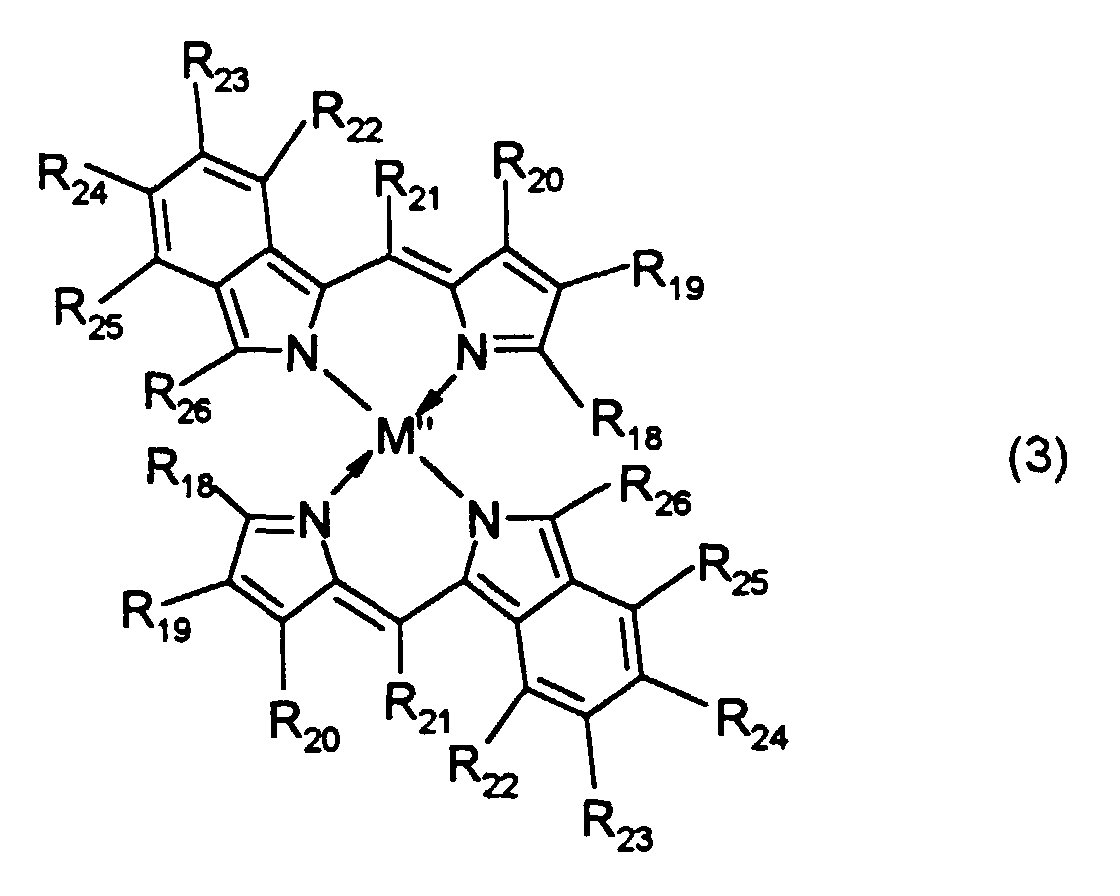
- R 19 to R 25 are each independently a hydrogen atom, a halogen atom, a nitro group, a cyano group, a hydroxyl group, an amino group, a carboxyl group, a sulfonic acid group, or a substituted or unsubstituted alkyl, alkoxy, alkylthio, aryloxy, arylthio, alkenyl, acyl, alkoxycarbonyl, carbamoyl, acylamino or aralkyl group having 20 or less carbon atoms.
- R 18 and R 26 are each independently an alkenyl group or an aryl group. Typical examples thereof include the above-mentioned groups.
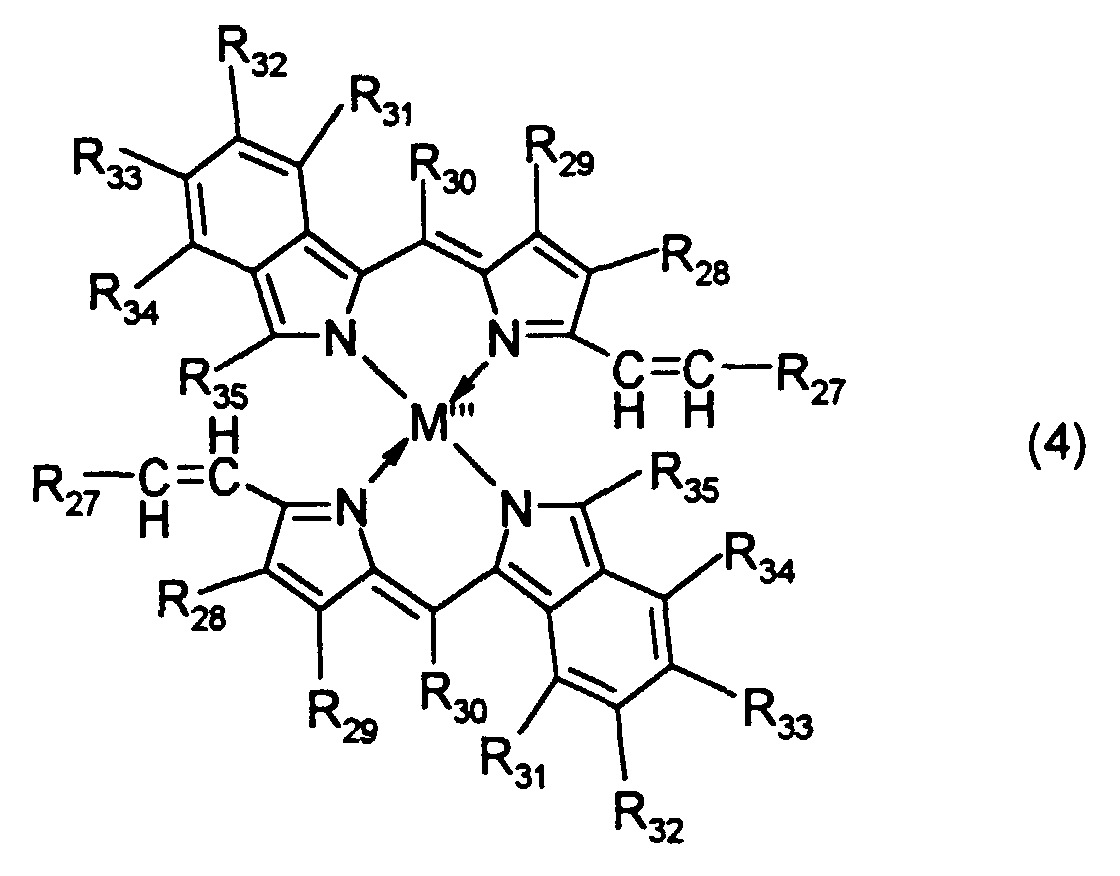
- R 27 to R 35 are each independently a hydrogen atom, a halogen atom, or a substituted or unsubstituted alkyl, alkoxy, alkenyl, acyl, alkoxycarbonyl, aralkyl, aryl or heteroaryl group having 20 or less carbon atoms. Typical examples thereof include the above-mentioned groups.
- M, M' and M''' are transition metals having an ability to form a chelate with the dipyrromethene compound, but examples thereof include metals in the groups 8, 9 and 10 (the group VIII), the group 11 (the group Ib), the group 12 (the group IIb), the group 3 (the group IIIa), the group 4 (the group IVa), the group 5 (the group Va), the group 6 (the group VIa) and the group 7 (the group VIIa) of the periodic table.
- Preferable examples thereof include nickel, cobalt, iron, ruthenium, rhodium, palladium, copper, osmium, iridium, platinum and zinc, and from the viewpoint of light resistance, particularly preferable examples include copper and cobalt.
- a method for preparing the dipyrromethene metal chelate compound represented by formula (1) of the present invention is not restricted, but for example, this compound can be prepared in accordance with any of methods described in Aust. J. Chem., Vol. 11, p. 1835-45 (1965), Heteroatom Chemistry, Vol. 1, No. 5, p. 389 (1990), U.S. Patent Nos. 4,774,339 and 5,433,896.
- the dipyrromethene metal chelate compound can be prepared by the following two step reactions.
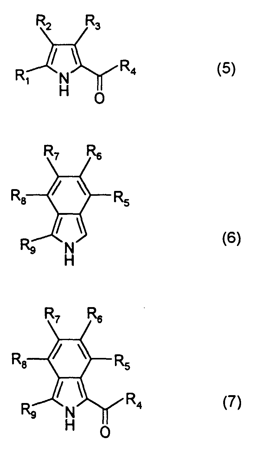
- a compound represented by formula (5) and a compound represented by formula (6), or a compound represented by formula (7) and a compound represented by formula (8) are reacted in the presence of an acid catalyst such as hydrobromic acid or hydrochloric acid in a suitable solvent, thereby obtaining a dipyrromethene compound represented by formula (9).
- the dipyrromethene compound of formula (9) is then reacted with an acetate or a halide of a metal such as nickel, cobalt, iron, ruthenium, rhodium, palladium, copper, osmium, iridium, platinum or zinc to obtain the dipyrromethene metal chelate compound represented by formula (1).
- Each of the compounds of formulae (2) to (4) can also be obtained by suitably altering substituents in a similar manner: wherein R 1 and R 9 are as defined above.
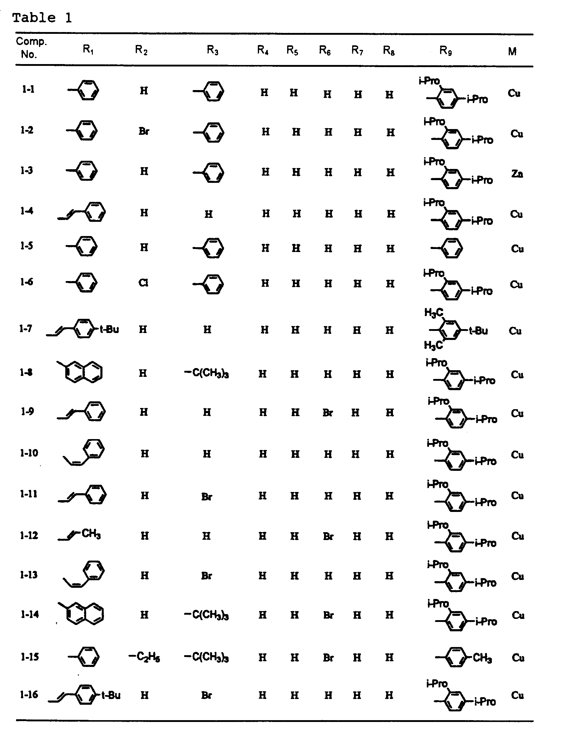
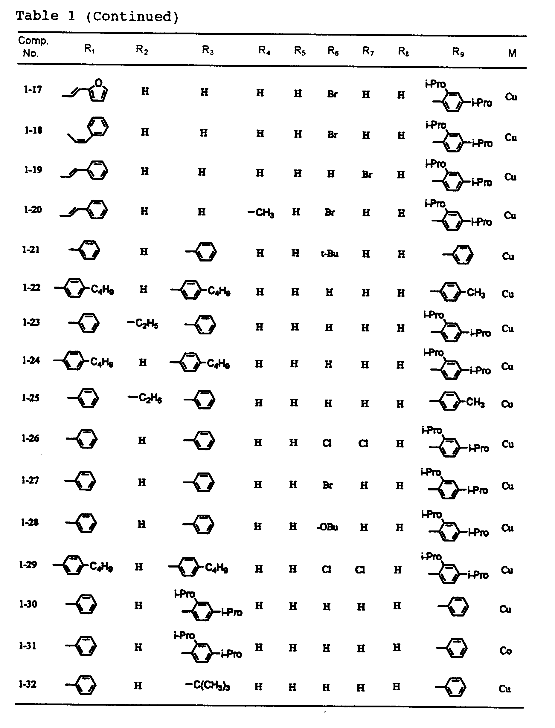
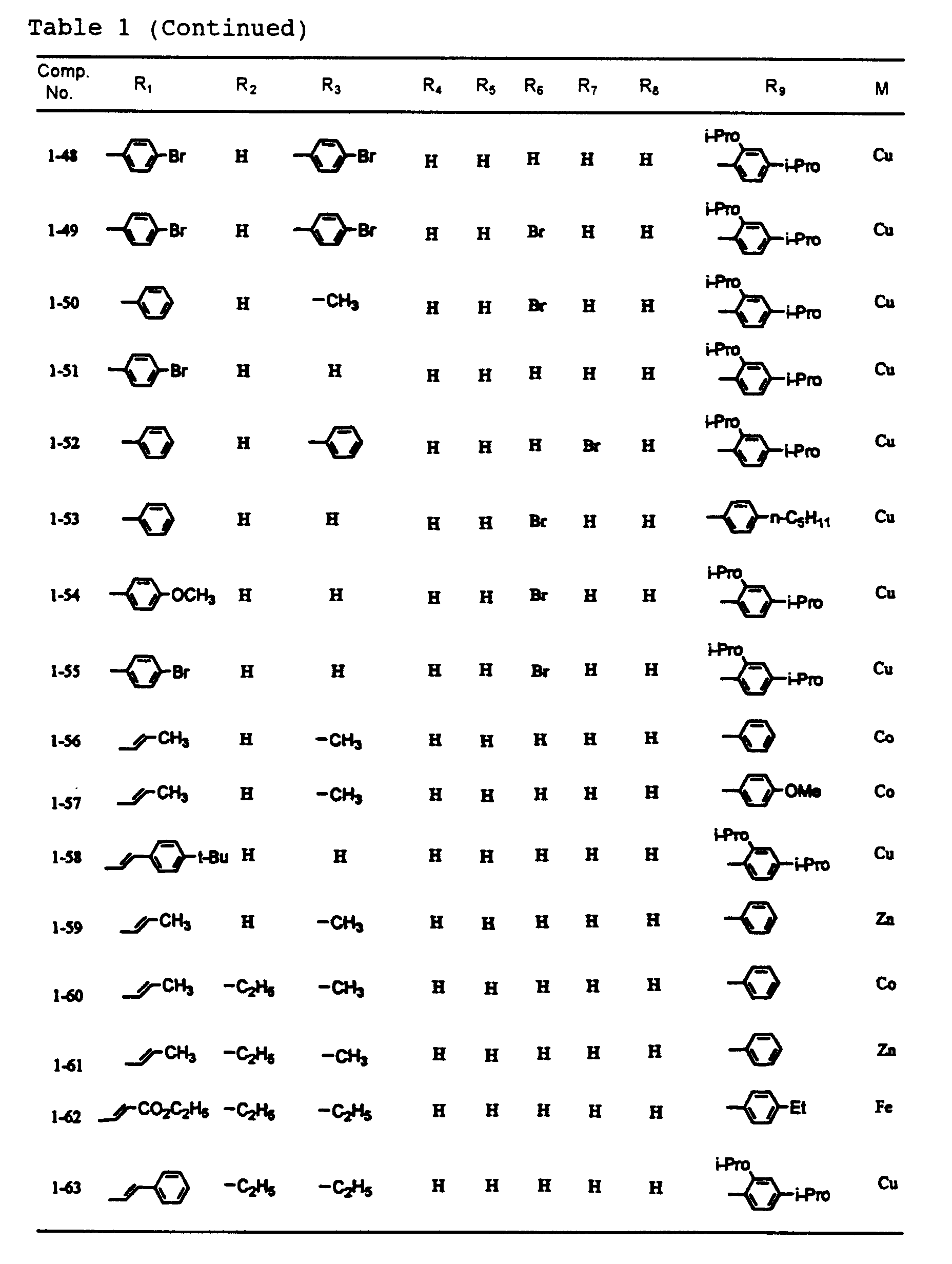
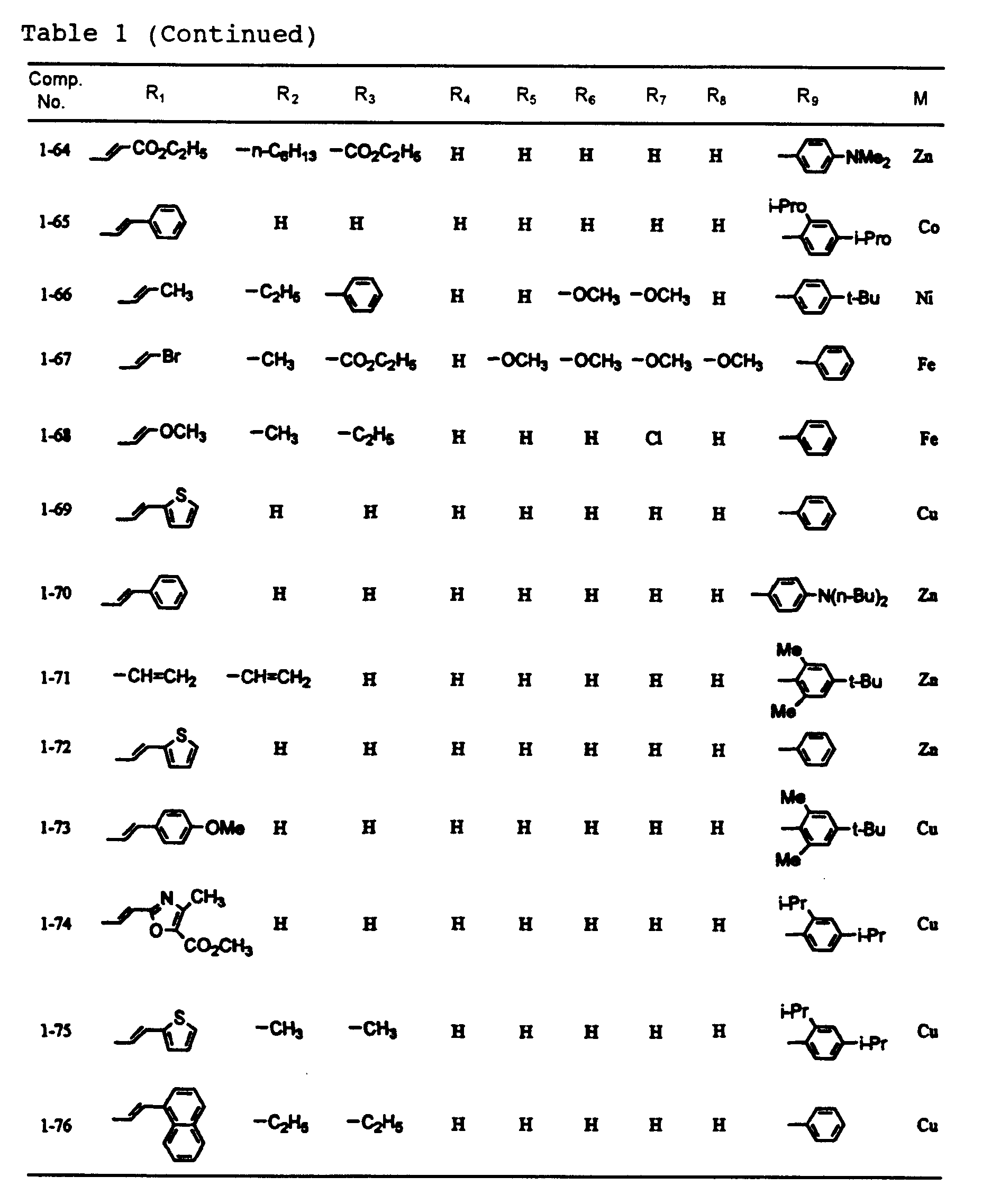
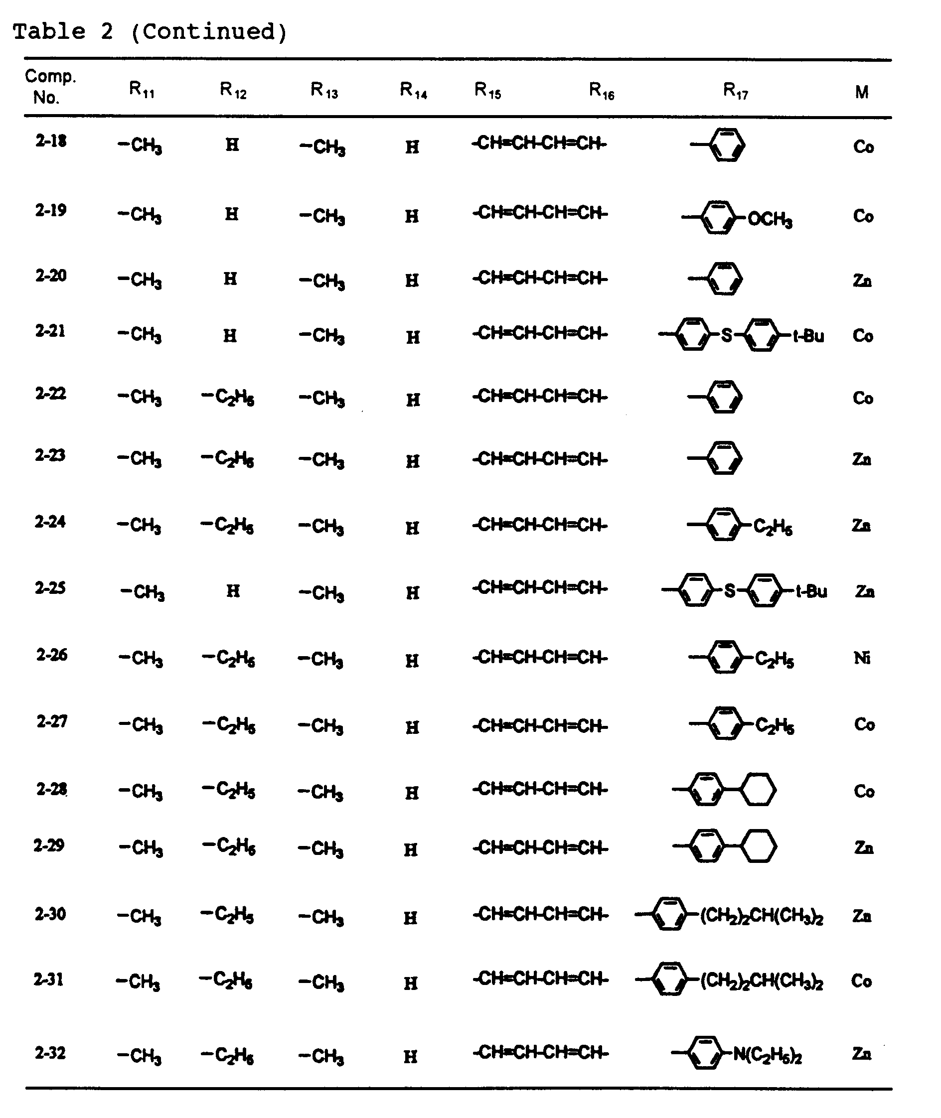
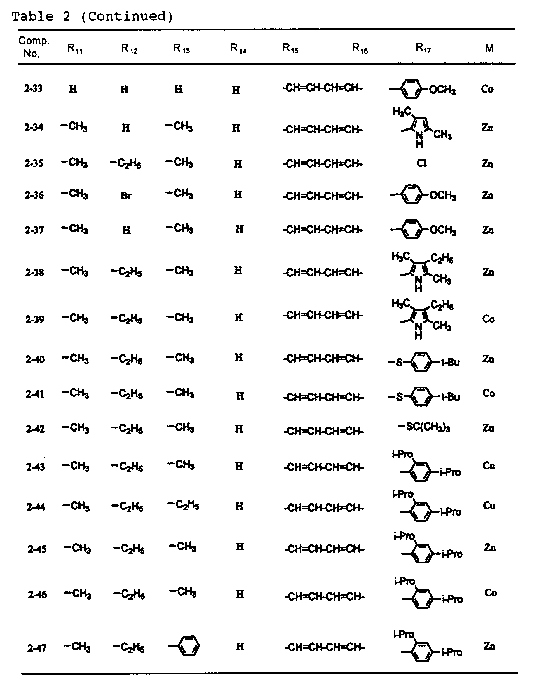
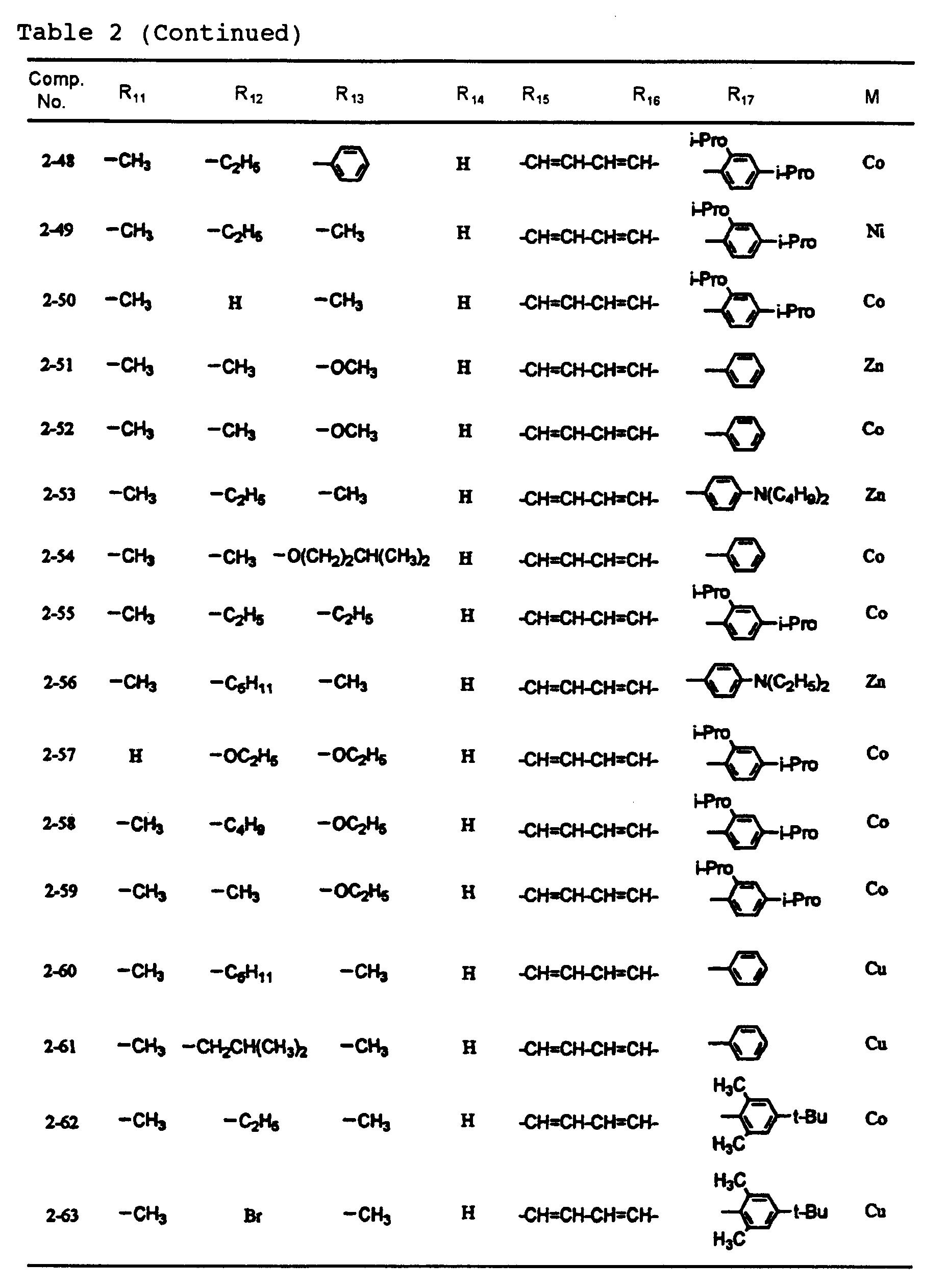
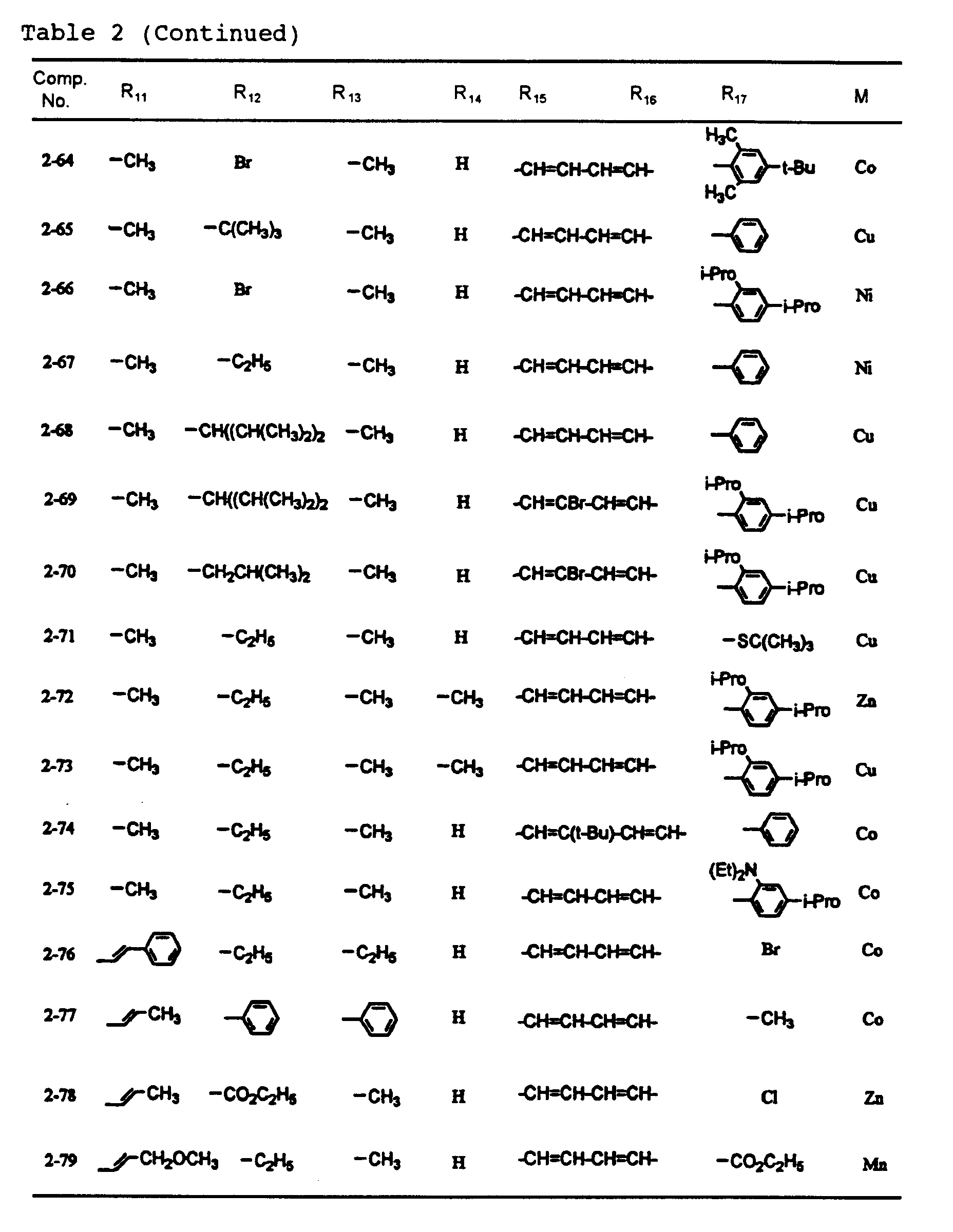
- dipyrromethene metal chelate compounds represented by formulae (1) to (3) of the present invention include compounds having substituents shown in Tables 1 to 3, respectively.
- An optical recording medium of the present invention has a laminate structure, as shown in Fig. 1. That is to say, a recording layer 2 is formed on a substrate 1, and a reflective layer 3 is closely disposed thereon. On this reflective layer 3, another substrate 5 is further stuck thereon via an adhesive layer 4. However, another layer may be formed under or on the recording layer 2, or another layer may be formed on the reflective layer 3.
- a material for the substrate should basically be transparent at wavelengths of a recording light and a reproduction light.
- a polymeric material such as a polycarbonate resin, a vinyl chloride resin, an acrylic resin such as polymethyl methacrylate, a polystyrene resin or an epoxy resin, or an inorganic material such as a glass.
- the substrate material is molded into disc substrates by injection molding or the like. If necessary, guide grooves or pits may be formed on the surface of the substrate. Such guide grooves or pits are desirably given at the time of the molding of the substrate, but they can be given by using an ultraviolet light setting resin layer on the substrate.
- the substrate is a disc having a thickness of about 1.2 mm, a diameter of about 80 to 120 mm, and a hole of 15 mm in diameter which is made through its center.
- the recording layer is formed on the substrate, and the recording layer of the present invention contains at least one dipyrromethene metal chelate compound represented by formula (1). More preferably, it further contains at least one dipyrromethene metal chelate compound represented by formula (2), and best preferably, it further contains at least one dipyrromethene metal chelate compound represented by formula (3).
- the recording layer is required to have a suitable optical constant at a recording and a reproduction laser wavelength selected within 520 nm to 690 nm ⁇ the optical constant is represented by a complex index of refraction (n + ki) wherein n and k are coefficients corresponding to a real part n and an imaginary part k, respectively, and here, n and k are defined as a refractive index and an extinction coefficient, respectively ⁇ .
- an organic dye is characterized in that the refractive index n and the extinction coefficient k largely depend on a wavelength ⁇ .
- a value of the refractive index n is less than 1.8, a reflectance and a signal modulated amplitude necessary for the accurate reading of signals cannot be obtained, and even if the extinction coefficient k is in excess of 0.40, the reflectance deteriorates, so that not only a good reproducible signal cannot be obtained but also the signal easily changes by the reproduction light.
- the usual organic dye is not practical.
- a specific organic dye having the preferable optical constant at the desired laser wavelength should be selected. When such an organic dye is selected and used to form the recording layer, a medium having the high reflectance and the good sensitivity can be obtained.
- the dipyrromethene metal chelate compound represented by formula (1) which can be used in the present invention has the above preferable optical constant, and the employment of two or more kinds of dipyrromethene metal chelate compounds for the recording layer makes it easy to select the desired optical constant.
- a difference between maximum absorption wavelengths of these dipyrromethene metal chelate compounds, when two or more kinds of dipyrromethene metal chelate compounds are employed is preferably 100 nm or less, more preferably 60 nm or less. No particular restriction is put on a mixing ratio of these dipyrromethene metal chelate compounds, but for the above reason, it is preferable to mix them so that the optical constant n may 2.0 or more and the extinction coefficient k is in the range of 0.04 to 0.20.
- the reproduction of the optical recording medium of the present invention by the laser light selected within the range of 520 nm to 690 nm can usually be realized at a reflectance of 20%, and a reflectance of 30% or more is preferable.
- the above dye Prior to the formation of the recording layer, if necessary, the above dye can be mixed with a quencher, a decomposition accelerator, an ultraviolet light absorber, an adhesive and the like, or compounds having such effects can be introduced as substituents into the dye.
- Typical preferable examples of the quencher include metal complexes of acetylacetonates, bisdithiols such as bisdithio- ⁇ -diketones and bisphenyldithiols, thiocatechols, salicylaldehydeoximes and thiobisphenolates.
- amines are also suitable.
- Examples of the decomposition accelerator include metallic compounds such as metallic anti-knock agents, metallocene compounds and metal complexes of acetylacetonates.
- a binder a binder, a leveling agent and an anti-foaming agent can be used together.
- the binder include polyvinyl alcohol, polyvinyl pyrrolidone, nitrocellulose, cellulose acetate, ketone resins, acrylic resins, polystyrene resins, urethane resins, polyvinyl butyrals, polycarbonates and polyolefins.
- a layer comprising an inorganic material or a polymer may be formed on the substrate in order to improve the solvent resistance of the substrate, the reflectance and the record sensitivity.
- the content of the dipyrromethene metal chelate compounds represented by formulas (1) to (3) in the recording layer is 30% or more, preferably 60% or more. Incidentally, it is also preferable that the content is virtually 100%.
- Examples of a method for forming the recording layer include coating methods by spin coating, spraying, casting and immersing, a sputtering process, a chemical vapor deposition method and a vacuum vapor deposition method, but the coating method by spin coating is simple and hence preferable.
- a coating method such as the spin coating method
- a coating solution prepared by dissolving or dispersing the dipyrromethene metal chelate compounds represented by formulas (1) to (3) in a solvent so as to be in the range of 1 to 40% by weight, preferably 3 to 30% by weight, but in this case, it is preferable to select the solvent which does not damage the substrate.
- a solvent examples include alcoholic solvents such as methanol, ethanol, isopropyl alcohol, octafluoropentanol, allyl alcohol, methyl cellosolve, ethyl cellosolve and tetrafluoropropanol, aliphatic and alicyclic hydrocarbon solvents such as hexane, heptane, octane, decane, cyclohexane, methylcyclohexane, ethylcyclohexane and dimethylcyclohexane, aromatic hydrocarbon solvents such as toluene, xylene and benzene, halogenated hydrocarbon solvents such as carbon tetrachloride, chloroform, tetrachloroethane and dibromoethane, ether solvents such as diethyl ether, dibutyl ether, di-isopropyl ether and dioxanes, ketone solvent
- the dye for the recording layer can be dispersed in a polymeric thin film.
- any of the sputtering process, the chemical vapor deposition method and the vacuum vapor deposition method is effective.
- the thickness of the recording layer is preferably in the range of 50 nm to 300 nm. If the thickness of the recording layer is less than 50 nm, heat diffusion increases, so that the recording cannot be performed, or distortion occurs on a recording signal, and signal amplitude decreases. Furthermore, if the thickness of the recording layer is more than 300 nm, the reflectance declines, so that reproducible signal characteristics deteriorate.
- a reflective layer having a thickness of preferably 50 nm to 300 nm is formed on the recording layer.
- a material for the reflective layer should have a sufficiently high reflectance at the wavelength of the reproduction light.
- the reflective layer material include metals such as Au, Al, Ag, Cu, Ti, Cr, Ni, Pt, Ta, Cr and Pd, and they can be used singly or in the form of an alloy thereof. Above all, Au, Al and Ag have the high reflectance, and hence they are suitable for the materials for the reflective layer.
- the reflective layer may contain any of metals and metalloids such as Mg, Se, Hf, V, Nb, Ru, W, Mn, Re, Fe, Co, Rh, Ir, Zn, Cd, Ga, In, Si, Ge, Te, Pb, Po, Sn and Bi.
- metals and metalloids such as Mg, Se, Hf, V, Nb, Ru, W, Mn, Re, Fe, Co, Rh, Ir, Zn, Cd, Ga, In, Si, Ge, Te, Pb, Po, Sn and Bi.
- a material including Au as a main component is suitable, because such a material makes it possible to easily obtain the reflective layer having the high reflectance.
- the main component means that the content of the component is more than 50%.
- a material other than the above metals can also be used, and for example, a multi-layer film formed by alternately laminating a thin film having a low refractive index and a thin film having a high refractive index can also be used as the reflective layer.
- Examples of a method for forming the reflective layer include the sputtering process, an ion plating method, the chemical vapor deposition method and the vacuum vapor deposition method.
- a known inorganic or organic intermediate layer or an adhesive layer can be deposited for the sake of the improvement of the reflectance, the recording characteristics and adhesive properties.
- a protective layer is formed on the reflective layer, and no particular restriction is put on a material for the protective layer, so long as it can protect the reflective layer from an outer force.
- a material for the protective layer include thermoplastic resins, thermosetting resins, electron beam curable resins and ultraviolet light curable resins.
- examples of an inorganic material for the protective layer include SiO 2 , Si 3 N 4 , MgF 2 and SnO 2 . The thermoplastic resin or the thermosetting resin is dissolved in a suitable solvent, and the resultant coating solution is applied and then dried to form the protective layer.
- the ultraviolet light curable resin may be directly applied, or it may be dissolved in a suitable solvent to prepare a coating solution, and this coating solution may be then applied and then irradiated with ultraviolet light to cure it, thereby forming the protective layer.
- the ultraviolet light curable resin include acrylate resins such as urethane acrylates, epoxy acrylates and polyester acrylates. These materials may be used singly or in the form of a mixture thereof, or they may be used in the form of a single layer or a multi-layer film.
- Examples of a method for forming the protective layer include coating methods by spin coating and casting, the sputtering process and the chemical vapor deposition method, as in the case of the recording layer, but above all, the spin coating method is preferable.
- the thickness of the protective layer is usually in the range of 0.1 ⁇ m to 100 ⁇ m, but in the present invention, it is preferably in the range of 3 ⁇ m to 30 ⁇ m, more preferably 5 ⁇ m to 20 ⁇ m.
- a print such as a label can be further carried out.
- a protective sheet or a substrate may be struck on the reflective layer, or there may be used a means in which the reflective layers are set so as to face each other, and two optical recording media may be then stuck.
- an ultraviolet light curable resin, an inorganic thin film or the like may be formed for the protection of the surface and the prevention of dust deposition.
- a laser having wavelengths of 520 nm to 690 nm referred to in the present invention examples include a dye laser which permits a wavelength selection in a wide visible light range, a helium neon laser having a wavelength of 633 nm, a high output semiconductor laser having wavelengths of about 680, 650 and 635 nm which has been recently developed, and a harmonic conversion YAG laser having a wavelength of 532 nm.
- a high-density recording and reproduction can be realized at one wavelength or plural wavelengths selected from these lasers.
- 0.2 g of a dipyrromethene metal chelate compound (1-4) was dissolved in 10 ml of dimethylcyclohexane to prepare a dye solution.
- a substrate which was used therein was made of a polycarbonate resin and had a continuous guide groove (track pitch: 0.8 ⁇ m), a diameter of 120 mm, a thickness of 0.6 mm and a disc shape.
- This substrate was spin-coated with this dye solution at a rotational speed of 1500 rpm, and it was then dried at 70 °C for 3 hours to form a recording layer.
- n and k at 635 nm were 2.3 and 0.11, respectively.
- Au was sputtered by the use of a sputter device (CDI-900) made by Bulzars Co., Ltd., thereby forming a reflective layer having a thickness of 100 nm.
- a sputter gas argon gas was used. With regard to sputter conditions, sputter power was 2.5 kW, and a sputter gas pressure was 1.0 ⁇ 10 -2 Torr.
- an ultraviolet light curable adhesive SD-301 (made by Dainippon Ink & Chemicals, Inc.) was spin-coated on the reflective layer, and on this adhesive film, there was put a disc substrate made of the polycarbonate resin and having a diameter of 120 mm and a thickness of 0.6 mm. Afterward, irradiation was made with ultraviolet light to obtain a stuck optical recording medium.
- optical recording medium On the thus obtained optical recording medium, recording was carried out at a linear velocity of 3.8 m/s and a laser power of 10 mW so that a shortest pit length might be 0.40 ⁇ m by the use of an optical disc evaluation device (DDU-1000) made by Pulstec Industrial Co., Ltd. carrying a semiconductor laser head in which a numerical aperture of a lens was 0.6 at a wavelength of 635 nm and an EFM encoder made by KENWOOD Co., Ltd. After the recording, signals were reproduced by an evaluation device carrying 650 nm and 635 nm red semiconductor laser heads (the numerical aperture of the lens was 0.6), and reflectance, jitter and modulated amplitude were then measured.
- DDU-1000 optical disc evaluation device
- EFM encoder made by KENWOOD Co., Ltd.
- An optical recording medium was prepared by the same procedure as in Example 1 except that there was used a disc substrate made of a polycarbonate resin and having a continuous guide groove (track pitch: 0.74 ⁇ m), a diameter of 120 mm and a thickness of 0.6 mm.
- optical recording medium On the thus obtained optical recording medium, recording was carried out in the same manner as in Example 1 by the use of an optical disc evaluation device (DDU-1000) made by Pulstec Industrial Co., Ltd. and an EFM encoder made by KENWOOD Co., Ltd. After the recording, signals were reproduced by an evaluation device carrying a 650 nm red semiconductor laser head, and reflectance, jitter and modulated amplitude were then measured. As a result, these values were all good, and the reflectance was 56%, the jitter was 8.6%, and the modulated amplitude was 0.62 in the case of the reproduction at 650 nm.
- DDU-1000 optical disc evaluation device
- EFM encoder made by KENWOOD Co., Ltd.
- An optical recording medium was prepared by the same procedure as in Example 1 except that each of dipyrromethene metal chelate compounds shown in Tables 1 and 2 was used, and recording was then carried out. After the recording, signals were reproduced by an evaluation device carrying a 650 nm red semiconductor laser head, and reflectance, jitter and modulated amplitude were then measured. As a result, these values were all good. In addition, even after a light resistance test for 100 hours by carbon arc and a wet heat resistance test at 80 °C and 85%RH, any change was not observed. Moreover, even when the reproduction was repeated million times under a reproduction light of 0.7 mW, the change of the jitter was 1% or less.
- An optical recording medium was prepared by the same procedure as in Example 2 except that dipyrromethene metal chelate compounds shown in Tables 1 to 3 were suitably mixed and used, and recording was then carried out. After the recording, signals were reproduced by an evaluation device carrying a 650 pm red semiconductor laser head, and reflectance, jitter and modulated amplitude were then measured. As a result, these values were all good. In addition, even after a light resistance test for 100 hours by carbon arc and a wet heat resistance test at 80°C and 85%RH, any change was not observed. Moreover, even when the reproduction was repeated million times under a reproduction light of 0.7 mW, the change of the jitter was 1% or less.
- An optical recording medium was prepared by the same procedure as in Example 1 except that 0.2 g of a dipyrromethene metal chelate compound (2-43) was dissolved in 10 ml of dimethylcyclohexane, followed by spin coat. On the thus obtained optical recording medium, recording was carried out in the same manner as in Example 1 at a linear velocity of 3.8 m/s and a laser power of 10 mW by the use of an optical disc evaluation device (DDU-1000) made by Pulstec Industrial Co., Ltd. carrying a 635 nm semiconductor laser head and an EFM encoder made by KENWOOD Co., Ltd.
- DDU-1000 optical disc evaluation device
- An optical recording medium was prepared by the same procedure as in Example 1 except that 0.2 g of a dipyrromethene metal chelate compound (2-23) was dissolved in 10 ml of dimethylcyclohexane, followed by spin coat. On the thus obtained optical recording medium, recording was carried out in the same manner as in Example 1 at a linear velocity of 3.8 m/s and a laser power of 10 mW by the use of an optical disc evaluation device (DDU-1000) made by Pulstec Industrial Co., Ltd. carrying a 635 nm semiconductor laser head and an EFM encoder made by KENWOOD Co., Ltd.
- DDU-1000 optical disc evaluation device
- An optical recording medium was prepared by the same procedure as in Example 1 except that 1 g of a pentamethinecyanine dye "NK-2929" [1,3,3,1',3',3'-hexamethyl-2',2'-(4,5,4',5'-dibenzo)indodicarbocyane perchlorate made by Nippon Kankou Shikiso Laboratory Co., Ltd.] was dissolved in 10 ml of tetrafluoropropanol, followed by spin coating.
- NK-2929 a pentamethinecyanine dye [1,3,3,1',3',3'-hexamethyl-2',2'-(4,5,4',5'-dibenzo)indodicarbocyane perchlorate made by Nippon Kankou Shikiso Laboratory Co., Ltd.] was dissolved in 10 ml of tetrafluoropropanol, followed by spin coating.
- Example 2 On the thus obtained optical recording medium, recording was carried out in the same manner as in Example 1 at a linear velocity of 3.8 m/s and a laser power of 10 mW by the use of an optical disc evaluation device (DDU-1000) made by Pulstec Industrial Co., Ltd. carrying a 635 nm semiconductor laser head and an EFM encoder made by KENWOOD Co., Ltd. After the recording, signals were reproduced by an evaluation device carrying a 650 nm red semiconductor laser head, and reflectance, jitter and modulated amplitude were then measured. As a result, in the case of the reproduction at 650 nm, the reflectance was 9%, the jitter was 20% or more, and the modulated amplitude was 0.13. Hence, these values were poor. In addition, after a light resistance test for 100 hours by carbon arc, the signals deteriorated, so that the reproduction was impossible.
- DDU-1000 optical disc evaluation device
- EFM encoder made by KENWOOD Co., Ltd.
- each mixing ratio means such a weight ratio of the dipyrromethene metal compound that a concentration of the dipyrromethene metal compound is 20 g/l with respect to dimethylcyclohexane.
- the thus obtained compound showed a maximum absorption at 589 nm in a toluene solution and had a Gram absorbancy index of 1.30 ⁇ 10 5 ml/g.cm.
- the thus obtained compound showed a maximum absorption at 588 nm in a toluene solution and had a Gram absorbancy index of 1.15 ⁇ 10 5 ml/g.cm.
- the thus obtained compound showed a maximum absorption at 595 nm in a toluene solution and had a Gram absorbancy index of 1.05 ⁇ 10 5 ml/g.cm.
- the thus obtained compound showed a maximum absorption at 575 nm in a toluene solution and had a Gram absorbancy index of 1.50 ⁇ 10 5 ml/g.cm.
- the thus obtained compound showed a maximum absorption at 602 nm in a toluene solution and had a Gram absorbancy index of 1.57 ⁇ 10 5 ml/g.cm.
- the thus obtained compound showed a maximum absorption at 597 nm in a toluene solution and had a Gram absorbancy index of 1.72 ⁇ 10 5 ml/g.cm.
Abstract

Description
- The present invention relates to an optical recording medium in which a dipyrromethene metal chelate compound is used and which is recordable and reproducible at a higher density as compared with a conventional case.
- Presently, as an optical recording medium having a larger capacity as compared with a CD, a digital video disc (DVD) having a capacity of 4.7 GB has been developed and commercialized. The DVD is a ROM medium, and hence, recordable and reproducible optical record media having the corresponding capacity are desired. Among the DVDs, a write-once type is called a DVD-R.
- In the DVD, in order to achieve a high-density recording, an oscillation wavelength of a laser beam is in the range of about 630 nm to 680 nm which are shorter wavelengths than in the case of the CD. As dyes for organic dye-including optical recording media which can be used within such short wavelengths, there have been suggested cyanine dyes, azo dyes, benzopyran-type dyes, benzodifuranone-type dyes, indigoid dyes, dioxazine-type dyes and porphyrin-type dyes in Japanese Patent Application Laid-open Nos. 74690/1992, 38878/1993, 40161/1994, 40162/1994, 199045/1994, 336086/1994, 76169/1995, 125441/1995, 262604/1995, 156218/1997, 193544/1997, 193545/1997, 193547/1997, 194748/1997, 202052/1997, 267562/1997 and 274732/1997. However, these conventional techniques have the problem of dye durability and particularly some problems peculiar to the uses of short wavelengths. For example, when a small pit is opened with a focussed laser beam, its periphery is widely affected, so that the largely expanded pit is inconveniently formed. This inconvenience causes the deterioration of a jitter and a radial cross talk. Conversely, in some of these conventional techniques, the extremely small pit is formed on occasion, and this inconvenience causes the deterioration of a modulated amplitude. In addition, when an organic dye having an unsuitable optical constant (a refractive index and an extinction coefficient) is selected and used for a recording layer at a desired laser wavelength, the deterioration of reflectance, sensitivity and the like occurs. Presently, these drawbacks have not been overcome at all yet.
- An object of the present invention is to provide an optical recording medium which is recordable and reproducible by a short wave laser having a wavelength of 520 to 690 nm, is excellent in durability, and is suitable for a high-density recording.
- The present inventors have already suggested a recordable and reproducible optical recording medium suitable for a high-density record, and in this kind of recording medium, a dipyrromethene metal chelate compound is used as an organic dye (Japanese Patent Application Laid-Open No. 226172/1998). The present inventors have further intensively investigated on the optical recording medium in which the dipyrromethene metal chelate compound is used. As a result, it has been found that a selection of a dipyrromethene metal chelate compound having a substituent containing a vinyl group or a halogen atom, a substituent such as a specific aryl group or heteroaryl group into the α-position of pyrrole ring, or copper or cobalt as a coordination metal in the above dipyrromethene metal chelate compound, and the use of two or more kinds of the selected dipyrromethene metal chelate compounds in a recording layer can provide an optical recording medium, in which the deterioration of reflectance and sensitivity caused by a drawback of the organic dye, i.e., a wavelength dependence of optical characteristics is inhibited and which is excellent in jitter properties and durability. In consequence, the present invention has been attained. That is to say, the aspects of the present invention are as follows.
- 1. The first aspect of the present invention is directed
to an optical recording medium having at least a recording layer
and a reflective layer on a substrate, wherein at least one
dipyrromethene metal chelate compound represented by formula (1)
is contained in the recording layer:
wherein R1 and R9 are each independently an alkenyl group, an aryl group or a heteroaryl group; R2 to R8 are each independently a hydrogen atom, a halogen atom, or a substituted or unsubstituted alkyl, alkoxy, alkenyl, acyl, alkoxycarbonyl, aralkyl, aryl or heteroaryl group having 20 or less carbon atoms; and M is a transition metal.

- 2. The second aspect of the present invention is
directed to the optical recording medium according to the
above paragraph 1 wherein R1 in formula (1) is -CH=CH-R10, wherein R10 is a hydrogen atom, a halogen atom, or a substituted or unsubstituted alkyl, alkoxy, alkenyl, acyl, alkoxycarbonyl, aralkyl, aryl or heteroaryl group having 20 or less carbon atoms. - 3. The third aspect of the present invention is directed
to the optical recording medium according to the
above paragraph 1 wherein R1 in formula (1) is a substituted or unsubstituted aryl or heteroaryl group having 20 or less carbon atoms, and M is copper or cobalt. - 4. The fourth aspect of the present invention is
directed to the optical recording medium according to the
above paragraph 3 wherein R1 and R3 in formula (1) are simultaneously substituted or unsubstituted aryl or heteroaryl groups having 20 or less carbon atoms. - 5. The fifth aspect of the present invention is directed
to the optical recording medium according to the
above paragraph 4 wherein R1, R3 and R9 in formula (1) are substituted or unsubstituted aryl groups having 20 or less carbon atoms, and at least one of the aryl groups is substituted by a halogen, or at least one of R2, R4 to R8 is a halogen atom. - 6. The sixth aspect of the present invention is directed
to the optical recording medium according to any one of the
above paragraphs 1 to 5 wherein the recording layer further includes at least one other dipyrromethene metal chelate compound represented by formula (2):wherein R11 to R17 are each independently a hydrogen atom, a halogen atom, a nitro group, a cyano group, a hydroxyl group, an amino group, a carboxyl group, a sulfonic acid group, or a substituted or unsubstituted alkyl, alkoxy, alkylthio, aryloxy, arylthio, alkenyl, acyl, alkoxycarbonyl, carbamoyl, acylamino, aralkyl, aryl or heteroaryl group having 20 or less carbon atoms, and R15 and R16 may be bonded to each other to form an aromatic ring which may have at least one substituent; and M' is a transition element.
- 7. The seventh aspect of the present invention is
directed to the optical recording medium according to the above
paragraph 6 wherein the other dipyrromethene metal chelate
compound is selected from compounds represented by formula (3):
wherein R19 to R25 are each independently a hydrogen atom, a halogen atom, a nitro group, a cyano group, a hydroxyl group, an amino group, a carboxyl group, a sulfonic acid group, or a substituted or unsubstituted alkyl, alkoxy, alkylthio, aryloxy, arylthio, alkenyl, acyl, alkoxycarbonyl, carbamoyl, acylamino or aralkyl group having 20 or less carbon atoms; R18 and R26 are each independently an alkenyl group or an aryl group; and M'' is copper or cobalt.
- 8. The eighth aspect of the present invention is
directed to the optical recording medium according to any one
of the
above paragraphs 1 to 7 wherein at a laser wavelength of 520 to 690 nm, a refractive index and an extinction coefficient of the recording layer are 1.8 or more and 0.04 to 0.40, respectively. - 9. The ninth aspect of the present invention is directed
to the optical recording medium according to any one of the
above paragraphs 1 to 7 which is recordable and reproducible by a laser beam selected within the wavelength range of 520 to 690 nm. - 10. A dipyrromethene metal chelate compound
represented by formula (4):
wherein R27 to R35 are each independently a hydrogen atom, a halogen atom, or a substituted or unsubstituted alkyl, alkoxy, alkenyl, acyl, alkoxycarbonyl, aralkyl, aryl or heteroaryl group having 20 or less carbon atoms; and M''' is a transition element.
-
- The employment of at least one dipyrromethene metal chelate compound of the present invention as a recording layer enables the provision of a write-once type optical recording medium which is very noticed as a high-density recording medium and which is recordable and reproducible by a laser beam having a wavelength of 520 to 690 nm and which is excellent in durability.
-
- Fig. 1 is a sectional structure view illustrating layer constitutions of optical recording media of a conventional case and the present invention.
-
- Now, the present invention will be described in detail.
- In a dipyrromethene metal chelate compound represented by formula (1), R1 and R9 are each independently an alkenyl group, an aryl group or a heteroaryl group, and R2 to R8 are each independently a hydrogen atom, a halogen atom, or a substituted or unsubstituted alkyl, alkoxy, alkenyl, acyl, alkoxycarbonyl, aralkyl, aryl or heteroaryl group having 20 or less carbon atoms.
- Examples of the aryl group represented by R1 and R9 include substituted and unsubstituted aryl groups having 20 or less carbon atoms such as a phenyl group, nitrophenyl groups, cyanophenyl groups, hydroxyphenyl groups, methylphenyl groups, ethylphenyl groups, n-butylphenyl groups, t-butylphenyl groups, cyclohexylphenyl groups, 2,4-dimethylphenyl group, 2,4-diisopropylphenyl group, 2,4,6-trimethylphenyl group, 2,6-dimethyl-4-t-butylphenyl group, fluorophenyl groups, chlorophenyl groups, bromophenyl groups, iodophenyl groups, 2,4-difluorophenyl group, 2,4-dichlorophenyl group, 2,4-dibromophenyl group, 2,4-diiodophenyl group, methoxyphenyl groups, ethoxyphenyl groups, n-butoxyphenyl groups, iso-amyloxyphenyl groups, trifluoromethylphenyl groups, N,N-dimethylaminophenyl groups, N,N-diethylaminophenyl groups, N,N-dibutylaminophenyl groups, 2-N,N-diethylamino-4-isopropylphenyl group, naphthyl group, nitronaphthyl groups, cyanonaphthyl groups, hydroxynaphthyl groups, methylnaphthyl groups, methoxynaphthyl groups, chloronaphthyl groups, bromonaphthyl groups and trifluoromethylnaphthyl groups;
and examples of the heteroaryl group represented by R1 and R9 include substituted and unsubstituted heteroaryl groups having 20 or less carbon atoms such as a pyrolyl groups, thienyl groups, furanyl groups, oxazoyl groups, isooxazoyl groups, oxadiazoyl groups, thiadiazoyl groups, imidazoyl groups, benzoxazoyl groups, benzothiazoyl groups, benzoimidazoyl groups, benzofuranyl groups and indoyl groups. - Examples of the alkenyl group represented by R1 and R9 include alkenyl groups which may have a substituent, and preferable examples thereof are represented by -CH=CHR10, wherein R10 is a hydrogen atom, a halogen atom, or a substituted or unsubstituted alkyl, alkoxy, alkenyl, acyl, alkoxycarbonyl, aralkyl, aryl or heteroaryl group having 20 or less carbon atoms.
- Typical examples of R10 include a hydrogen atom; halogen atoms such as fluorine, chlorine, bromine and iodine; substituted and unsubstituted alkyl groups having 20 or less carbon atoms such as a methyl group, ethyl group, n-propyl group, iso-propyl group, n-butyl group, iso-butyl group, sec-butyl group, t-butyl group, n-pentyl group, iso-pentyl group, 2-methylbutyl group, 1-methylbutyl group, neo-pentyl group, 1,2-dimethylpropyl group, 1,1-dimethylpropyl group, cyclopentyl group, n-hexyl group, 4-methylpentyl group, 3-methylpentyl group, 2-methylpentyl group, 1-methylpentyl group, 3,3-dimethylbutyl group, 2,3-dimethylbutyl group, 1,3-dimethylbutyl group, 2,2-dimethylbutyl group, 1,2-dimethylbutyl group, 1,1-dimethylbutyl group, 3-ethylbutyl group, 2-ethylbutyl group, 1-ethylbutyl group, 1,2,2-trimethylbutyl group, 1,1,2-trimethylbutyl group, 1-ethyl-2-methylpropyl group, cyclo-hexyl group, n-heptyl group, 2-methylhexyl group, 3-methylhexyl group, 4-methylhexyl group, 5-methylhexyl group, 2,4-dimethylpentyl group, n-octyl group, 2-ethylhexyl group, 2,5-dimethylhexyl group, 2,5,5-trimethylpentyl group, 2,4-dimethylhexyl group, 2,2,4-trimethylpentyl group, 3,5,5-trimethylhexyl group, n-nonyl group, n-decyl group, 4-ethyloctyl group, 4-ethyl-4,5-dimethylhexyl group, n-undecyl group, n-dodecyl group, 1,3,5,7-tetraethyloctyl group, 4-butyloctyl group, 6,6-diethyloctyl group, n-tridecyl group, 6-methyl-4-butyloctyl group, n-tetradecyl group, n-pentadecyl group, 3,5-dimethylheptyl group, 2,6-dimethylheptyl group, 2,4-dimethylheptyl group, 2,2,5,5-tetramethylhexyl group, 1-cyclopentyl-2,2-dimethylpropyl group, 1-cyclohexyl-2,2-dimethylpropyl group, chloromethyl group, dichloromethyl group, fluoromethyl group, trifluoromethyl group, pentafluoroethyl group and nonafluorobuty group;
substituted and unsubstituted alkoxy groups having 20 or less carbon atoms such as a methoxy group, ethoxy group, n-propoxy group, iso-propoxy group, n-butoxy group, iso-butoxy group, sec-butoxy group, t-butoxy group, n-pentoxy group, iso-pentoxy group, neo-pentoxy group, n-hexyloxy group, n-dodecyloxy group, methoxyethoxy group, ethoxyethoxy group, 3-methoxypropyloxy group and 3-(iso-propyloxy)propyloxy group;
substituted and unsubstituted alkenyl groups having 20 or less carbon atoms such as a vinyl group, propenyl group, 1-butenyl group, iso-butenyl group, 1-pentenyl group, 2-pentenyl group, 2-methyl-1-butenyl group, 3-methyl-1-butenyl group, 2-methyl-2-butenyl group, 2,2-dicyanovinyl group, 2-cyano-2-methylcarboxyvinyl group and 2-cyano-2-methylsulfonevinyl group;
substituted and unsubstituted acyl groups having 20 or less carbon atoms such as a formyl group, acetyl group, ethylcarbonyl group, n-propylcarbonyl group, iso-propylcarbonyl group, n-butylcarbonyl group, n-pentylcarbonyl group, iso-pentylcarbonyl group, neo-pentylcarbonyl group, 2-methylbutylcarbonyl group and nitrobenzylcarbonyl group;
substituted and unsubstituted alkoxycarbonyl groups having 20 or less carbon atoms such as a methoxycarbonyl group, ethoxycarbonyl group, isopropyloxycarbonyl group and 2,4-dimethylbutyloxycarbonyl group; and
substituted and unsubstituted aralkyl groups having 20 or less carbon atoms such as a benzyl group, nitrobenzyl groups, cyanobenzyl groups, hydroxybenzyl groups, methylbenzyl groups, dimethylbenzyl group, trimethylbenzyl group, dichlorobenzyl group, methoxybenzyl groups, ethoxybenzyl groups, trifluoromethylbenzyl groups, naphthylmethyl group, nitronaphthylmethyl groups, cyanonaphthylmethyl groups, hydroxynaphthylmethyl groups, methylnaphthylmethyl groups and trifluoromethylnaphthylmethyl groups;
the aryl groups; and the heteroaryl groups mentioned above. - Typical examples of R2 to R8 include a hydrogen atom; halogen atoms such as fluorine, chlorine, bromine and iodine;
and the alkyl groups, the alkoxy groups, the alkenyl groups, the acyl groups, the alkoxycarbonyl groups, the aralkyl groups, the aryl groups and the heteroaryl groups mentioned above. - In the dipyrromethene metal chelate compound represented by formula (2), R11 to R17 are each independently a hydrogen atom, a halogen atom, a nitro group, a cyano group, a hydroxyl group, an amino group, a carboxyl group, a sulfonic acid group, or a substituted or unsubstituted alkyl, alkoxy, alkylthio, aryloxy, arylthio, alkenyl, acyl, alkoxycarbonyl, carbamoyl, acylamino, aralkyl, aryl or heteroaryl group having 20 or less carbon atoms. Here, R15 and R16 may be bonded to each other to form an aromatic ring which may have a substituent or substituents.
- Examples of the halogen atom, the alkyl group, the alkoxy group, the alkenyl group, the acyl group, the alkoxycarbonyl group, the aralkyl group, the aryl group and the heteroaryl group include those which are mentioned above.
- Furthermore, typical examples of the alkylthio group represented by R11 to R17 include alkylthio groups such as a methylthio group, ethylthio group, n-propylthio group, iso-propylthio group, n-butylthio group, iso-butylthio group, sec-butylthio group, t-butylthio group, n-pentylthio group, iso-pentylthio group, 2-methylbutylthio group, 1-methylbutylthio group, neo-pentylthio group, 1,2-dimethylpropylthio group and 1,1-dimethylpropylthio group;
typical examples of the aryloxy group represented by R11 to R17 include aryloxy groups such as a phenoxy group, 2-methylphenoxy group, 4-methylphenoxy group, 4-t-butylphenoxy group, 2-methoxyphenoxy group and 4-iso-propylphenoxy group;
typical examples of the arylthio group represented by R11 to R17 include arylthio groups such as a phenylthio group, 4-methylphenylthio group, 2-methoxyphenylthio group and 4-t-butylphenylthio group;
typical examples of the acylamino group represented by R11 to R17 include acylamino groups such as an acetylamino group, ethylcarbonylamino group, butylcarbonylamino group, phenylcarbonylamino group, 4-ethylphenylcarbonylamino group and 3-butylphenylcarbonylamino group;
and typical examples of the carbamoyl group represented by R11 to R17 include alkylaminocarbonyl groups such as a methylaminocarbonyl group, ethylaminocarbonyl group, n-propylaminocarbonyl group, n-butylaminocarbonyl group and n-hexylaminocarbonyl group, and phenylaminocarbonyl groups such as a phenylaminocarbonyl group, 4-methylphenylaminocarbonyl group, 2-methoxyphenylaminocarbonyl group and 4-n-propylphenylaminocarbonyl group. - In the dipyrromethene metal chelate compound represented by formula (3), R19 to R25 are each independently a hydrogen atom, a halogen atom, a nitro group, a cyano group, a hydroxyl group, an amino group, a carboxyl group, a sulfonic acid group, or a substituted or unsubstituted alkyl, alkoxy, alkylthio, aryloxy, arylthio, alkenyl, acyl, alkoxycarbonyl, carbamoyl, acylamino or aralkyl group having 20 or less carbon atoms. R18 and R26 are each independently an alkenyl group or an aryl group. Typical examples thereof include the above-mentioned groups.
- In the dipyrromethene metal chelate compound represented by formula (4), R27 to R35 are each independently a hydrogen atom, a halogen atom, or a substituted or unsubstituted alkyl, alkoxy, alkenyl, acyl, alkoxycarbonyl, aralkyl, aryl or heteroaryl group having 20 or less carbon atoms. Typical examples thereof include the above-mentioned groups.
- No particular restriction is put on typical examples of M, M' and M''', so long as they are transition metals having an ability to form a chelate with the dipyrromethene compound, but examples thereof include metals in the groups 8, 9 and 10 (the group VIII), the group 11 (the group Ib), the group 12 (the group IIb), the group 3 (the group IIIa), the group 4 (the group IVa), the group 5 (the group Va), the group 6 (the group VIa) and the group 7 (the group VIIa) of the periodic table. Preferable examples thereof include nickel, cobalt, iron, ruthenium, rhodium, palladium, copper, osmium, iridium, platinum and zinc, and from the viewpoint of light resistance, particularly preferable examples include copper and cobalt.
- A method for preparing the dipyrromethene metal chelate compound represented by formula (1) of the present invention is not restricted, but for example, this compound can be prepared in accordance with any of methods described in Aust. J. Chem., Vol. 11, p. 1835-45 (1965), Heteroatom Chemistry, Vol. 1, No. 5, p. 389 (1990), U.S. Patent Nos. 4,774,339 and 5,433,896. Typically, the dipyrromethene metal chelate compound can be prepared by the following two step reactions.
- In the first step, a compound represented by formula (5) and a compound represented by formula (6), or a compound represented by formula (7) and a compound represented by formula (8) are reacted in the presence of an acid catalyst such as hydrobromic acid or hydrochloric acid in a suitable solvent, thereby obtaining a dipyrromethene compound represented by formula (9). Next, in the second step, the dipyrromethene compound of formula (9) is then reacted with an acetate or a halide of a metal such as nickel, cobalt, iron, ruthenium, rhodium, palladium, copper, osmium, iridium, platinum or zinc to obtain the dipyrromethene metal chelate compound represented by formula (1). Each of the compounds of formulae (2) to (4) can also be obtained by suitably altering substituents in a similar manner:
 wherein R1 and R9 are as defined above.
- Preferable typical examples of the dipyrromethene metal chelate compounds represented by formulae (1) to (3) of the present invention include compounds having substituents shown in Tables 1 to 3, respectively.


- A concrete constitution of the present invention will be described hereinafter.
- An optical recording medium of the present invention has a laminate structure, as shown in Fig. 1. That is to say, a
recording layer 2 is formed on asubstrate 1, and areflective layer 3 is closely disposed thereon. On thisreflective layer 3, anothersubstrate 5 is further stuck thereon via anadhesive layer 4. However, another layer may be formed under or on therecording layer 2, or another layer may be formed on thereflective layer 3. - A material for the substrate should basically be transparent at wavelengths of a recording light and a reproduction light. For example, there can be utilized a polymeric material such as a polycarbonate resin, a vinyl chloride resin, an acrylic resin such as polymethyl methacrylate, a polystyrene resin or an epoxy resin, or an inorganic material such as a glass. The substrate material is molded into disc substrates by injection molding or the like. If necessary, guide grooves or pits may be formed on the surface of the substrate. Such guide grooves or pits are desirably given at the time of the molding of the substrate, but they can be given by using an ultraviolet light setting resin layer on the substrate. When used as a DVD, the substrate is a disc having a thickness of about 1.2 mm, a diameter of about 80 to 120 mm, and a hole of 15 mm in diameter which is made through its center.
- In the present invention, the recording layer is formed on the substrate, and the recording layer of the present invention contains at least one dipyrromethene metal chelate compound represented by formula (1). More preferably, it further contains at least one dipyrromethene metal chelate compound represented by formula (2), and best preferably, it further contains at least one dipyrromethene metal chelate compound represented by formula (3). Particularly, the recording layer is required to have a suitable optical constant at a recording and a reproduction laser wavelength selected within 520 nm to 690 nm {the optical constant is represented by a complex index of refraction (n + ki) wherein n and k are coefficients corresponding to a real part n and an imaginary part k, respectively, and here, n and k are defined as a refractive index and an extinction coefficient, respectively}.
- In general, an organic dye is characterized in that the refractive index n and the extinction coefficient k largely depend on a wavelength λ. When a value of the refractive index n is less than 1.8, a reflectance and a signal modulated amplitude necessary for the accurate reading of signals cannot be obtained, and even if the extinction coefficient k is in excess of 0.40, the reflectance deteriorates, so that not only a good reproducible signal cannot be obtained but also the signal easily changes by the reproduction light. Hence, the usual organic dye is not practical. In view of the above characteristics, a specific organic dye having the preferable optical constant at the desired laser wavelength should be selected. When such an organic dye is selected and used to form the recording layer, a medium having the high reflectance and the good sensitivity can be obtained.
- The dipyrromethene metal chelate compound represented by formula (1) which can be used in the present invention has the above preferable optical constant, and the employment of two or more kinds of dipyrromethene metal chelate compounds for the recording layer makes it easy to select the desired optical constant.
- From a practical viewpoint, a difference between maximum absorption wavelengths of these dipyrromethene metal chelate compounds, when two or more kinds of dipyrromethene metal chelate compounds are employed, is preferably 100 nm or less, more preferably 60 nm or less. No particular restriction is put on a mixing ratio of these dipyrromethene metal chelate compounds, but for the above reason, it is preferable to mix them so that the optical constant n may 2.0 or more and the extinction coefficient k is in the range of 0.04 to 0.20.
- The reproduction of the optical recording medium of the present invention by the laser light selected within the range of 520 nm to 690 nm can usually be realized at a reflectance of 20%, and a reflectance of 30% or more is preferable.
- Prior to the formation of the recording layer, if necessary, the above dye can be mixed with a quencher, a decomposition accelerator, an ultraviolet light absorber, an adhesive and the like, or compounds having such effects can be introduced as substituents into the dye.
- Typical preferable examples of the quencher include metal complexes of acetylacetonates, bisdithiols such as bisdithio-α-diketones and bisphenyldithiols, thiocatechols, salicylaldehydeoximes and thiobisphenolates. In addition, amines are also suitable.
- Examples of the decomposition accelerator include metallic compounds such as metallic anti-knock agents, metallocene compounds and metal complexes of acetylacetonates.
- Furthermore, if necessary, a binder, a leveling agent and an anti-foaming agent can be used together. Preferable examples of the binder include polyvinyl alcohol, polyvinyl pyrrolidone, nitrocellulose, cellulose acetate, ketone resins, acrylic resins, polystyrene resins, urethane resins, polyvinyl butyrals, polycarbonates and polyolefins.
- Prior to the formation of the recording layer on the substrate, a layer comprising an inorganic material or a polymer may be formed on the substrate in order to improve the solvent resistance of the substrate, the reflectance and the record sensitivity.
- Here, the content of the dipyrromethene metal chelate compounds represented by formulas (1) to (3) in the recording layer is 30% or more, preferably 60% or more. Incidentally, it is also preferable that the content is virtually 100%.
- Examples of a method for forming the recording layer include coating methods by spin coating, spraying, casting and immersing, a sputtering process, a chemical vapor deposition method and a vacuum vapor deposition method, but the coating method by spin coating is simple and hence preferable.
- In the case that a coating method such as the spin coating method is employed, there can be used a coating solution prepared by dissolving or dispersing the dipyrromethene metal chelate compounds represented by formulas (1) to (3) in a solvent so as to be in the range of 1 to 40% by weight, preferably 3 to 30% by weight, but in this case, it is preferable to select the solvent which does not damage the substrate. Examples of such a solvent include alcoholic solvents such as methanol, ethanol, isopropyl alcohol, octafluoropentanol, allyl alcohol, methyl cellosolve, ethyl cellosolve and tetrafluoropropanol, aliphatic and alicyclic hydrocarbon solvents such as hexane, heptane, octane, decane, cyclohexane, methylcyclohexane, ethylcyclohexane and dimethylcyclohexane, aromatic hydrocarbon solvents such as toluene, xylene and benzene, halogenated hydrocarbon solvents such as carbon tetrachloride, chloroform, tetrachloroethane and dibromoethane, ether solvents such as diethyl ether, dibutyl ether, di-isopropyl ether and dioxanes, ketone solvents such as acetone and 3-hydroxy-3-methyl-2-butanone, ester solvents such as ethyl acetate and methyl lactate, and water. They may be used singly or in the state of a mixture thereof.
- As needed, the dye for the recording layer can be dispersed in a polymeric thin film.
- When the solvent which does not damage the substrate cannot be selected, any of the sputtering process, the chemical vapor deposition method and the vacuum vapor deposition method is effective.
- No particular restriction is put on the thickness of the recording layer, but it is preferably in the range of 50 nm to 300 nm. If the thickness of the recording layer is less than 50 nm, heat diffusion increases, so that the recording cannot be performed, or distortion occurs on a recording signal, and signal amplitude decreases. Furthermore, if the thickness of the recording layer is more than 300 nm, the reflectance declines, so that reproducible signal characteristics deteriorate.
- Next, a reflective layer having a thickness of preferably 50 nm to 300 nm is formed on the recording layer. A material for the reflective layer should have a sufficiently high reflectance at the wavelength of the reproduction light. Examples of the reflective layer material include metals such as Au, Al, Ag, Cu, Ti, Cr, Ni, Pt, Ta, Cr and Pd, and they can be used singly or in the form of an alloy thereof. Above all, Au, Al and Ag have the high reflectance, and hence they are suitable for the materials for the reflective layer. In addition thereto, the reflective layer may contain any of metals and metalloids such as Mg, Se, Hf, V, Nb, Ru, W, Mn, Re, Fe, Co, Rh, Ir, Zn, Cd, Ga, In, Si, Ge, Te, Pb, Po, Sn and Bi. Furthermore, a material including Au as a main component is suitable, because such a material makes it possible to easily obtain the reflective layer having the high reflectance. Here, the main component means that the content of the component is more than 50%. A material other than the above metals can also be used, and for example, a multi-layer film formed by alternately laminating a thin film having a low refractive index and a thin film having a high refractive index can also be used as the reflective layer.
- Examples of a method for forming the reflective layer include the sputtering process, an ion plating method, the chemical vapor deposition method and the vacuum vapor deposition method. In addition, on the substrate or under the reflective layer, a known inorganic or organic intermediate layer or an adhesive layer can be deposited for the sake of the improvement of the reflectance, the recording characteristics and adhesive properties.
- Moreover, a protective layer is formed on the reflective layer, and no particular restriction is put on a material for the protective layer, so long as it can protect the reflective layer from an outer force. Examples of an organic material for the protective layer include thermoplastic resins, thermosetting resins, electron beam curable resins and ultraviolet light curable resins. Furthermore, examples of an inorganic material for the protective layer include SiO2, Si3N4, MgF2 and SnO2. The thermoplastic resin or the thermosetting resin is dissolved in a suitable solvent, and the resultant coating solution is applied and then dried to form the protective layer. The ultraviolet light curable resin may be directly applied, or it may be dissolved in a suitable solvent to prepare a coating solution, and this coating solution may be then applied and then irradiated with ultraviolet light to cure it, thereby forming the protective layer. Examples of the ultraviolet light curable resin include acrylate resins such as urethane acrylates, epoxy acrylates and polyester acrylates. These materials may be used singly or in the form of a mixture thereof, or they may be used in the form of a single layer or a multi-layer film.
- Examples of a method for forming the protective layer include coating methods by spin coating and casting, the sputtering process and the chemical vapor deposition method, as in the case of the recording layer, but above all, the spin coating method is preferable.
- The thickness of the protective layer is usually in the range of 0.1 µm to 100 µm, but in the present invention, it is preferably in the range of 3 µm to 30 µm, more preferably 5 µm to 20 µm.
- On the protective layer, a print such as a label can be further carried out.
- Alternatively, a protective sheet or a substrate may be struck on the reflective layer, or there may be used a means in which the reflective layers are set so as to face each other, and two optical recording media may be then stuck.
- In addition, on the mirror surface of the substrate, an ultraviolet light curable resin, an inorganic thin film or the like may be formed for the protection of the surface and the prevention of dust deposition.
- No particular restriction is put on a laser having wavelengths of 520 nm to 690 nm referred to in the present invention, but examples of such a laser include a dye laser which permits a wavelength selection in a wide visible light range, a helium neon laser having a wavelength of 633 nm, a high output semiconductor laser having wavelengths of about 680, 650 and 635 nm which has been recently developed, and a harmonic conversion YAG laser having a wavelength of 532 nm. In the present invention, at one wavelength or plural wavelengths selected from these lasers, a high-density recording and reproduction can be realized.
- Next, the present invention will be described in accordance with some examples, but the scope of the present invention should not be limited at all by these examples.
- 0.2 g of a dipyrromethene metal chelate compound (1-4) was dissolved in 10 ml of dimethylcyclohexane to prepare a dye solution. A substrate which was used therein was made of a polycarbonate resin and had a continuous guide groove (track pitch: 0.8 µm), a diameter of 120 mm, a thickness of 0.6 mm and a disc shape.
- This substrate was spin-coated with this dye solution at a rotational speed of 1500 rpm, and it was then dried at 70 °C for 3 hours to form a recording layer. With regard to an optical constant of this recording layer, n and k at 635 nm were 2.3 and 0.11, respectively.
- On this recording layer, Au was sputtered by the use of a sputter device (CDI-900) made by Bulzars Co., Ltd., thereby forming a reflective layer having a thickness of 100 nm. As a sputter gas, argon gas was used. With regard to sputter conditions, sputter power was 2.5 kW, and a sputter gas pressure was 1.0×10⁻² Torr.
- Furthermore, an ultraviolet light curable adhesive SD-301 (made by Dainippon Ink & Chemicals, Inc.) was spin-coated on the reflective layer, and on this adhesive film, there was put a disc substrate made of the polycarbonate resin and having a diameter of 120 mm and a thickness of 0.6 mm. Afterward, irradiation was made with ultraviolet light to obtain a stuck optical recording medium.
- On the thus obtained optical recording medium, recording was carried out at a linear velocity of 3.8 m/s and a laser power of 10 mW so that a shortest pit length might be 0.40 µm by the use of an optical disc evaluation device (DDU-1000) made by Pulstec Industrial Co., Ltd. carrying a semiconductor laser head in which a numerical aperture of a lens was 0.6 at a wavelength of 635 nm and an EFM encoder made by KENWOOD Co., Ltd. After the recording, signals were reproduced by an evaluation device carrying 650 nm and 635 nm red semiconductor laser heads (the numerical aperture of the lens was 0.6), and reflectance, jitter and modulated amplitude were then measured. As a result, these values were all good, and the reflectance was 56%, the jitter was 8.5%, and the modulated amplitude was 0.63 in the case of the reproduction at 650 nm. In addition, even after a light resistance test for 100 hours by carbon arc and a wet heat resistance test at 80°C and 85%RH, any change was not observed. Moreover, even when the reproduction was repeated million times under a reproduction light of 0.7 mW, the change of the jitter was 1% or less.
- An optical recording medium was prepared by the same procedure as in Example 1 except that there was used a disc substrate made of a polycarbonate resin and having a continuous guide groove (track pitch: 0.74 µm), a diameter of 120 mm and a thickness of 0.6 mm.
- On the thus obtained optical recording medium, recording was carried out in the same manner as in Example 1 by the use of an optical disc evaluation device (DDU-1000) made by Pulstec Industrial Co., Ltd. and an EFM encoder made by KENWOOD Co., Ltd. After the recording, signals were reproduced by an evaluation device carrying a 650 nm red semiconductor laser head, and reflectance, jitter and modulated amplitude were then measured. As a result, these values were all good, and the reflectance was 56%, the jitter was 8.6%, and the modulated amplitude was 0.62 in the case of the reproduction at 650 nm. In addition, even after a light resistance test for 100 hours by carbon arc and a wet heat resistance test at 80°C and 85%RH, any change was not observed. Moreover, even when the reproduction was repeated million times under a reproduction light of 0.7 mW, the change of the jitter was 1% or less.
- An optical recording medium was prepared by the same procedure as in Example 1 except that each of dipyrromethene metal chelate compounds shown in Tables 1 and 2 was used, and recording was then carried out. After the recording, signals were reproduced by an evaluation device carrying a 650 nm red semiconductor laser head, and reflectance, jitter and modulated amplitude were then measured. As a result, these values were all good. In addition, even after a light resistance test for 100 hours by carbon arc and a wet heat resistance test at 80 °C and 85%RH, any change was not observed. Moreover, even when the reproduction was repeated million times under a reproduction light of 0.7 mW, the change of the jitter was 1% or less.
- In Examples 1 to 87 described above, optical constants of recording layers as well as reflectances, jitters and modulated amplitudes in the case that the respective optical record media were recorded at 635 nm and reproduced at 650 nm are shown all together in Table 4.

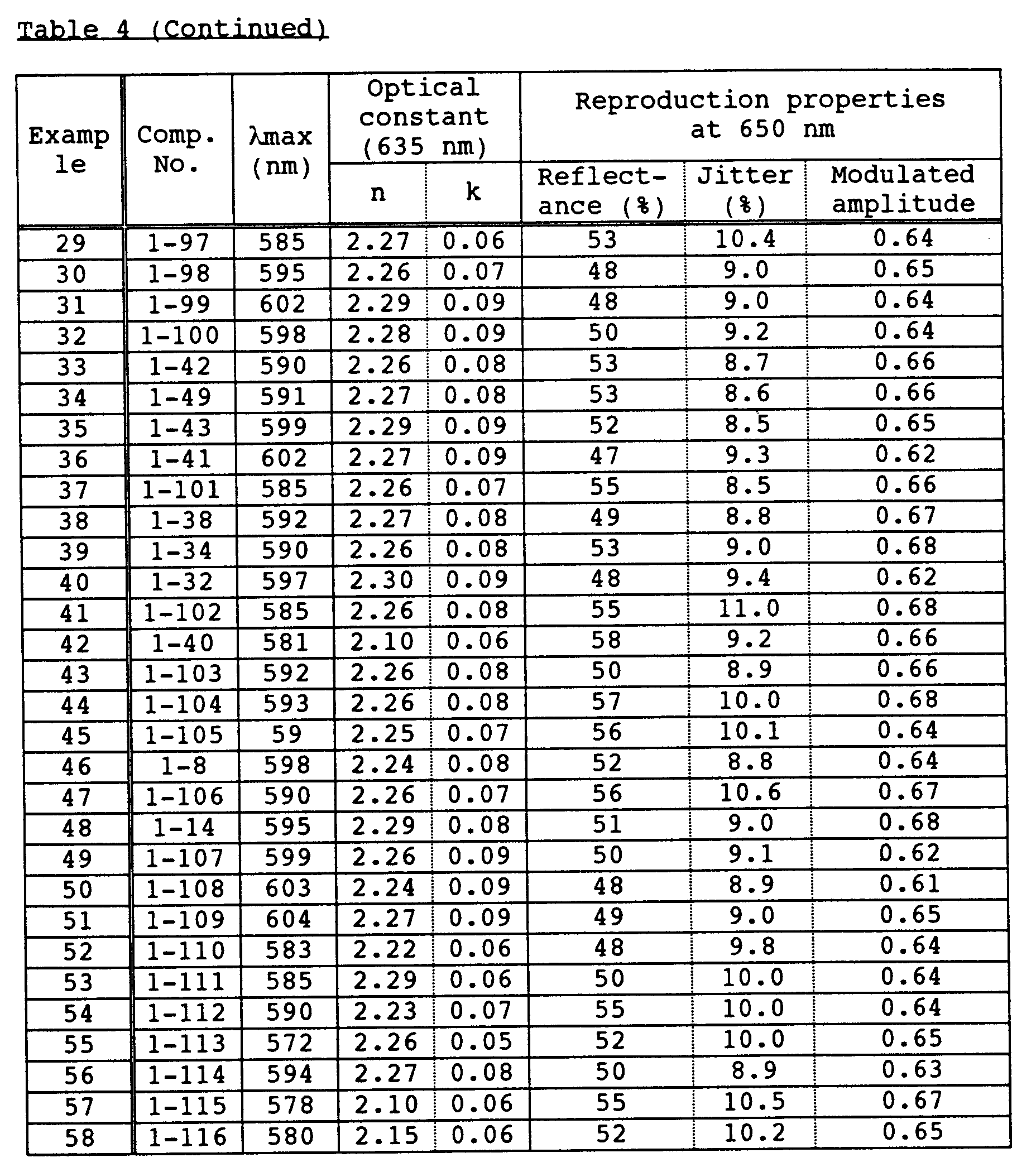

- An optical recording medium was prepared by the same procedure as in Example 2 except that dipyrromethene metal chelate compounds shown in Tables 1 to 3 were suitably mixed and used, and recording was then carried out. After the recording, signals were reproduced by an evaluation device carrying a 650 pm red semiconductor laser head, and reflectance, jitter and modulated amplitude were then measured. As a result, these values were all good. In addition, even after a light resistance test for 100 hours by carbon arc and a wet heat resistance test at 80°C and 85%RH, any change was not observed. Moreover, even when the reproduction was repeated million times under a reproduction light of 0.7 mW, the change of the jitter was 1% or less.
- An optical recording medium was prepared by the same procedure as in Example 1 except that 0.2 g of a dipyrromethene metal chelate compound (2-43) was dissolved in 10 ml of dimethylcyclohexane, followed by spin coat. On the thus obtained optical recording medium, recording was carried out in the same manner as in Example 1 at a linear velocity of 3.8 m/s and a laser power of 10 mW by the use of an optical disc evaluation device (DDU-1000) made by Pulstec Industrial Co., Ltd. carrying a 635 nm semiconductor laser head and an EFM encoder made by KENWOOD Co., Ltd. After the recording, signals were reproduced by an evaluation device carrying a 650 nm red semiconductor laser head, and reflectance, jitter and modulated amplitude were then measured. As a result, in the case of the reproduction at 650 nm, the reflectance was 61%, the jitter was 20% or more, and the modulated amplitude was 0.64. Thus, the jitter properties were poor.
- An optical recording medium was prepared by the same procedure as in Example 1 except that 0.2 g of a dipyrromethene metal chelate compound (2-23) was dissolved in 10 ml of dimethylcyclohexane, followed by spin coat. On the thus obtained optical recording medium, recording was carried out in the same manner as in Example 1 at a linear velocity of 3.8 m/s and a laser power of 10 mW by the use of an optical disc evaluation device (DDU-1000) made by Pulstec Industrial Co., Ltd. carrying a 635 nm semiconductor laser head and an EFM encoder made by KENWOOD Co., Ltd. After the recording, signals were reproduced by an evaluation device carrying 650 nm and 635 nm red semiconductor laser heads, and reflectance, jitter and modulated amplitude were then measured. As a result, in the case of the reproduction at 650 nm, the reflectance was 60%, the jitter was 20% or more, and the modulated amplitude was 0.65, and in the case of the reproduction at 635 nm, the reflectance was 61%, the jitter was 20% or more, and the modulated amplitude was 0.66. Thus, the jitter properties were poor. In addition, after a light resistance test for 100 hours by carbon arc, the signals deteriorated, so that the reproduction was impossible.
- An optical recording medium was prepared by the same procedure as in Example 1 except that 1 g of a pentamethinecyanine dye "NK-2929" [1,3,3,1',3',3'-hexamethyl-2',2'-(4,5,4',5'-dibenzo)indodicarbocyane perchlorate made by Nippon Kankou Shikiso Laboratory Co., Ltd.] was dissolved in 10 ml of tetrafluoropropanol, followed by spin coating. On the thus obtained optical recording medium, recording was carried out in the same manner as in Example 1 at a linear velocity of 3.8 m/s and a laser power of 10 mW by the use of an optical disc evaluation device (DDU-1000) made by Pulstec Industrial Co., Ltd. carrying a 635 nm semiconductor laser head and an EFM encoder made by KENWOOD Co., Ltd. After the recording, signals were reproduced by an evaluation device carrying a 650 nm red semiconductor laser head, and reflectance, jitter and modulated amplitude were then measured. As a result, in the case of the reproduction at 650 nm, the reflectance was 9%, the jitter was 20% or more, and the modulated amplitude was 0.13. Hence, these values were poor. In addition, after a light resistance test for 100 hours by carbon arc, the signals deteriorated, so that the reproduction was impossible.
- In Examples 88 to 106 and Comparative Examples 1 to 3 described above, optical constants of recording layers as well as reflectances, jitters and modulated amplitudes in the case that the respective optical record media were recorded at 635 nm and reproduced at 650 nm are shown all together in Table 5 (Examples) and Table 6 (Comparative Examples). In Table 5, each mixing ratio means such a weight ratio of the dipyrromethene metal compound that a concentration of the dipyrromethene metal compound is 20 g/l with respect to dimethylcyclohexane.
Example Comp. 1 (λmax (nm)) Comp. 2 (λmax (nm)) Dif. of λmax Mixing Ratio Optical constant Reproduction properties at 650 nm n k Reflectance (%) Jitter (%) Modulated amplitude 88 1-1 (580) 1-4 (602) 22 7:3 2.20 0.08 52 8.2 0.65 89 1-4 (602) 1-27 (591) 11 5:5 2.30 0.10 49 7.8 0.64 90 1-9 (614) 1-40 (582) 32 3:7 2.28 0.09 49 7.9 0.62 91 1-9 (614) 1-38 (581) 33 3:7 2.29 0.09 50 8.0 0.61 92 1-9 (614) 1-27 (591) 23 3:7 2.31 0.11 48 7.8 0.61 93 1-9 (614) 1-27 (591) 23 5:5 2.40 0.15 47 7.5 0.61 94 1-11 (607) 1-27 (591) 16 5:5 2.26 0.11 49 8.1 0.63 95 2-1 (510) 1-56 (553) 43 1:9 2.10 0.06 55 8.7 0.69 96 1-19 (616) 1-49 (589) 27 4:6 2.29 0.11 48 8.0 0.62 97 2-14 (521) 1-8 (598) 77 2:8 2.26 0.09 51 2.8 0.64 98 1-34 (590) 1-47 (596) 6 5:5 2.31 0.11 48 8.0 0.61 99 3-1 (610) 2-72 (561) 49 7:3 2.08 0.07 55 8.6 0.67 100 1-14 (595 2-74 (565) 30 7:3 2.26 0.09 49 7.9 0.62 101 2-43 (565) 1-17 (625) 60 2:8 2.25 0.08 52 8.0 0.61 102 1-13 (592) 1-55 (585) 7 6:4 2.29 0.12 48 8.1 0.63 103 1-15 (604) 2-73 (563) 41 8:2 2.13 0.09 50 8.3 0.65 104 2-5 (520) 1-7 (607) 87 1:9 2.15 0.08 51 8.4 0.64 105 1-4 (602) 1-38 (581) 21 3:7 2.39 0.13 47 7.6 0.64 106 3-1 (610) 1-40 (614) 4 6:4 2.35 0.12 48 7.7 0.63 Comparative Example Compound λmax (nm) Optical constant Reproduction properties at 650 nm n k Reflectance (%) Jitter (%) Modulated amplitude 1 2-43 565 2.00 0.04 61 20< 0.64 2 2-23 580 2.30 0.12 60 20< 0.65 3 NK2929 - 1.80 1.30 9 20< 0.13 - 1.35 g of 2-formyl-5-[(E)-phenylethen-1-yl]pyrrole and 1.9 g of 1-formyl-3-(2,4-diisopropylphenyl)isoindole were dissolved in 100 ml of ethanol, and 1.18 g of 47% hydrobromic acid was then added dropwise, followed by stirring at room temperature for 3 hours. After concentration under reduced pressure, extraction was carried out with 300 ml of chloroform, and after water washing and separation, the solvent was distilled off to obtain 3.0 g of a compound represented by the following structural formula (9-a):

- Next, 1.4 g of compound (9-a) were dissolved in 200 ml of ethanol, and 0.56 g of copper acetate was then added, followed by stirring for 2 hours at a reflux temperature. After concentration under reduced pressure, the resultant precipitate was collected by filtration, and then washed with methanol and water to obtain 1.2 g of a compound represented by the structural formula (1-4):
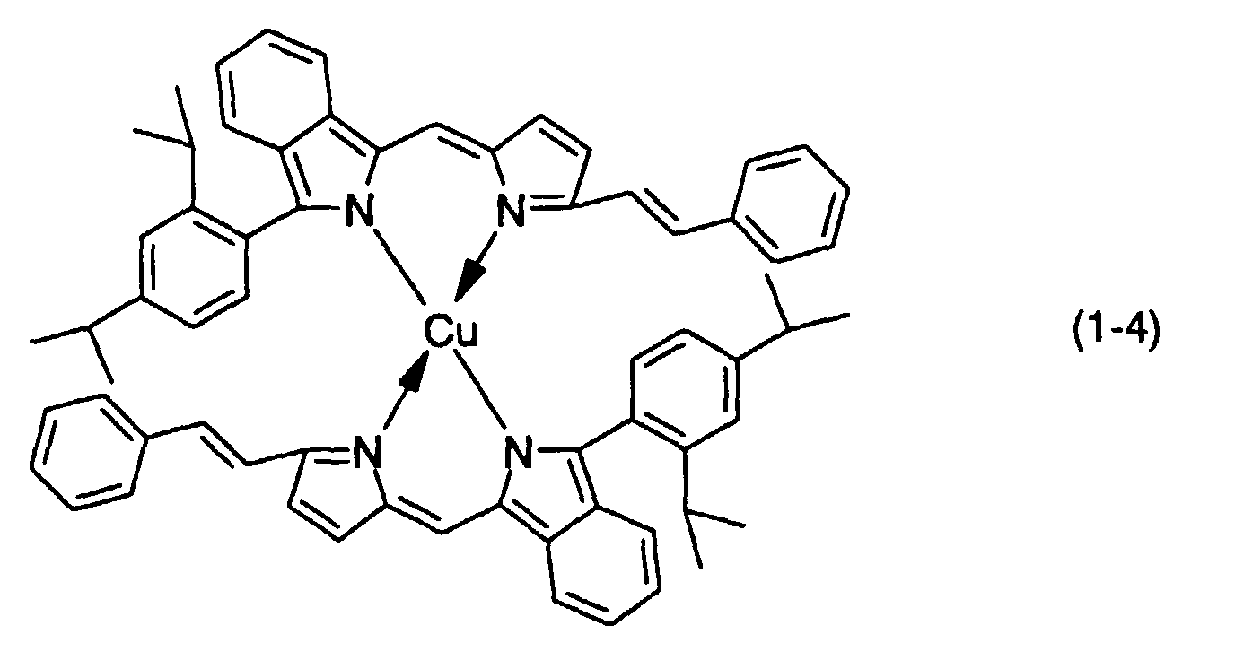
- It was confirmed on the basis of the following analytical results that the thus obtained compound was the desired compound.
Elemental analysis (C66H62N4Cu) C H N Calcd. (%) 81.32 6.41 5.75 Found (%) 81.82 6.61 5.69 - MS (m/e): 975 (M+)
-
- The thus obtained compound showed a maximum absorption at 589 nm in a toluene solution and had a Gram absorbancy index of 1.30×10⁵ ml/g.cm.
- 1.74 g of 2-formyl-5-[(E)-4-t-butylphenylethen-1-yl]pyrrole and 1.9 g of 1-formyl-3-(2,4-diisopropylphenyl)-isoindole were dissolved in 100 ml of ethanol, and 1.18 g of 47% hydrobromic acid was then added dropwise, followed by stirring at room temperature for 3 hours. After concentration under reduced pressure, extraction was carried out with 300 ml of chloroform, and after water washing and separation, the solvent was distilled off to obtain 3.1 g of a compound represented by the following structural formula (9-b):
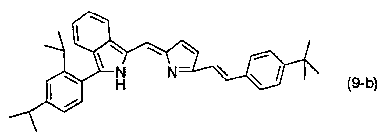
- Next, 1.57 g of compound (9-b) were dissolved in 200 ml of ethanol, and 0.56 g of copper acetate was then added, followed by stirring for 2 hours at a reflux temperature. After concentration under reduced pressure, the resultant precipitate was collected by filtration, and then washed with methanol and water to obtain 1.5 g of a compound represented by the structural formula (1-58):
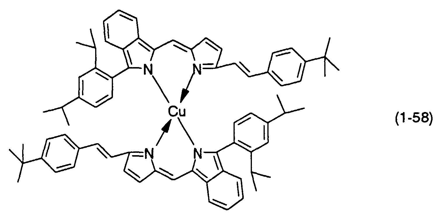
- It was confirmed on the basis of the following analytical results that the thus obtained compound was the desired compound.
Elemental analysis (C74H78N4Cu) C H N Calcd. (%) 81.77 7.23 5.15 Found (%) 81.48 7.46 5.22 - MS (m/e): 1087 (M+)
-
- The thus obtained compound showed a maximum absorption at 588 nm in a toluene solution and had a Gram absorbancy index of 1.15×10⁵ ml/g.cm.
- 1.74 g of 2-formyl-3,4-diethyl-5-[(E)-phenylethen-1-yl]pyrrole and 1.9 g of 1-formyl-3-(2,4-diisopropylphenyl)-isoindole were dissolved in 100 ml of ethanol, and 1.18 g of 47% hydrobromic acid was then added dropwise, followed by stirring at room temperature for 3 hours. After concentration under reduced pressure, extraction was carried out with 300 ml of chloroform, and after water washing and separation, the solvent was distilled off to obtain 3.1 g of a compound represented by the following structural formula (9-c):
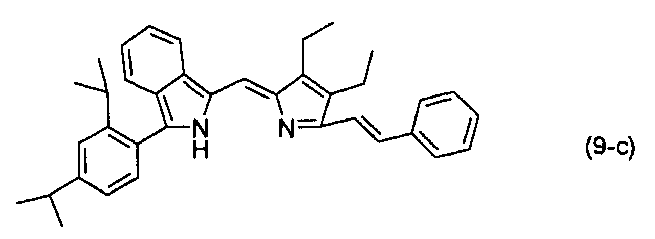
- Next, 1.57 g of compound (9-c) were dissolved in 200 ml of ethanol, and 0.56 g of copper acetate was then added, followed by stirring for 2 hours at a reflux temperature. After concentration under reduced pressure, the resultant precipitate was collected by filtration, and then washed with methanol and water to obtain 1.6 g of a compound represented by the structural formula (1-63):
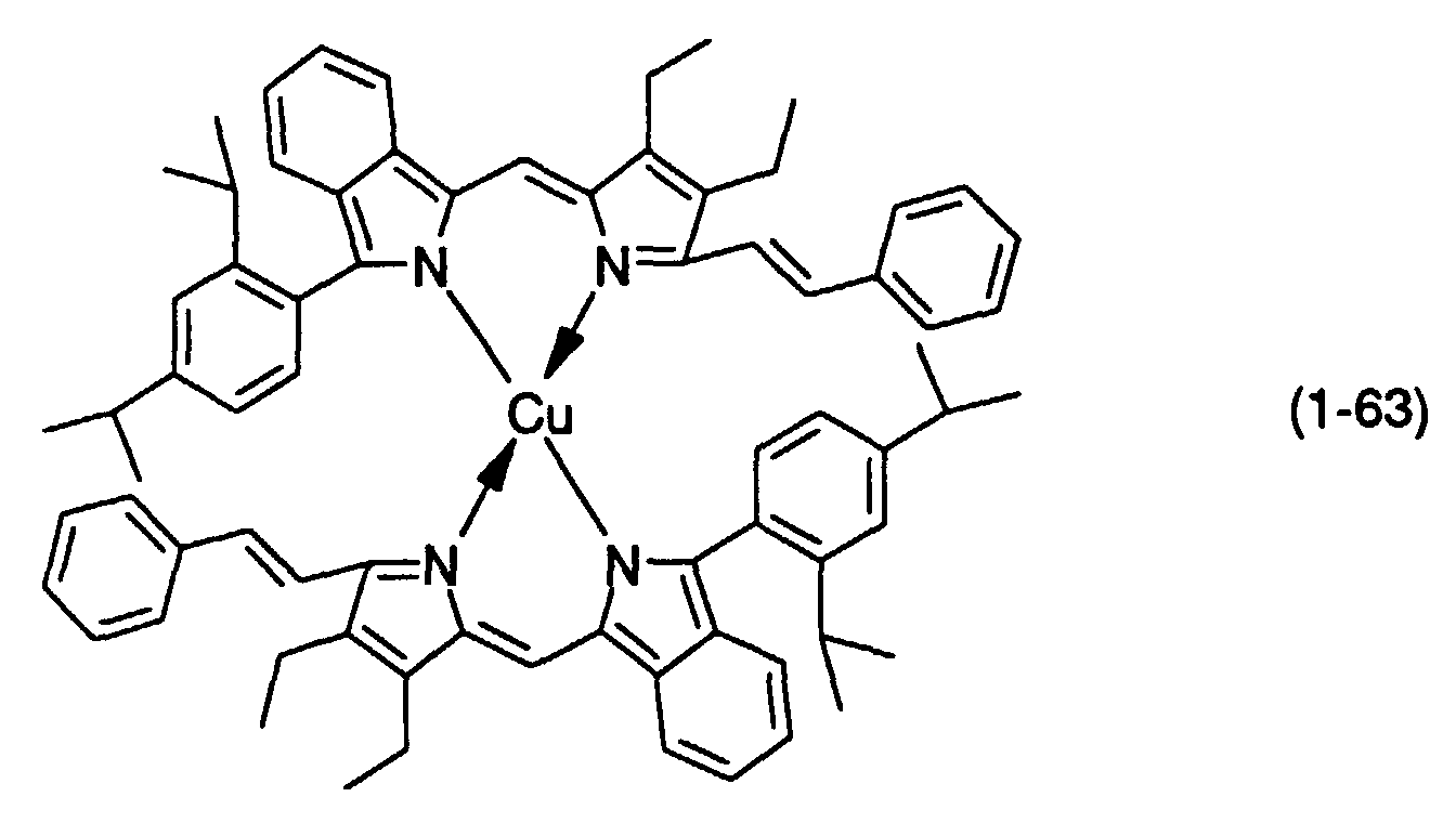
- It was confirmed on the basis of the following analytical results that the thus obtained compound was the desired compound.
Elemental analysis (C74H78N4Cu) C H N Calcd. (%) 81.77 7.23 5.15 Found (%) 81.52 7.52 5.33 - MS (m/e): 1087 (M+)
-
- The thus obtained compound showed a maximum absorption at 595 nm in a toluene solution and had a Gram absorbancy index of 1.05×10⁵ ml/g.cm.
- 1.4 g of a compound represented by formula (9-a) were dissolved in 100 ml of ethanol, and 0.76 g of cobalt acetate tetrahydrate was then added, followed by stirring at a reflux temperature for 4 hours. After concentration under reduced pressure, the resultant precipitate was collected by filtration, and then washed with methanol and water to obtain 1.3 g of a compound represented by the structural formula (1-65):
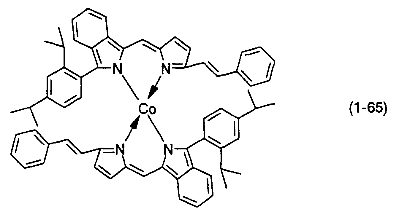
- It was confirmed on the basis of the following analytical results that the thus obtained compound was the desired compound.
Elemental analysis (C66H62N4Co) C H N Calcd. (%) 81.71 6.44 5.77 Found (%) 81.65 6.51 5.87 - MS (m/e): 970 (M+)
-
- The thus obtained compound showed a maximum absorption at 575 nm in a toluene solution and had a Gram absorbancy index of 1.50×10⁵ ml/g.cm.
- 1.39 g of 2-formyl-5-(2-thienylethen-1-yl)pyrrole and 1.32 g of 1-formyl-3-phenylisoindole were dissolved in 100 ml of ethanol, and 1.18 g of 47% hydrobromic acid was then added dropwise, followed by stirring at room temperature for 3 hours. After concentration under reduced pressure, extraction was carried out with 300 ml of chloroform, and after water washing and separation, the solvent was distilled off to obtain 2.6 g of a compound represented by the structural formula (9-d):

- Next, 1.2 g of compound (9-d) were dissolved in 200 ml of ethanol, and 0.56 g of copper acetate was then added, followed by stirring at a reflux temperature for 2 hours. After concentration under reduced pressure, the resultant precipitate was collected by filtration, and then washed with methanol and water to obtain 1.1 g of a compound represented by the structural formula (1-69):

- It was confirmed on the basis of the following analytical results that the thus obtained compound was the desired compound.
Elemental analysis (C50H34N4S2Cu) C H N S Calcd. (%) 73.37 4.19 6.84 7.83 Found (%) 73.56 4.33 6.75 8.00 - MS (m/e): 819 (M+)
-
- The thus obtained compound showed a maximum absorption at 602 nm in a toluene solution and had a Gram absorbancy index of 1.57×10⁵ ml/g.cm.
- 1.2 g of a compound represented by formula (9-d) were dissolved in 200 ml of ethanol, and 0.56 g of zinc acetate was then added, followed by stirring at a reflux temperature for 5 hours. After concentration under reduced pressure, the resultant precipitate was collected by filtration, and then washed with methanol and water to obtain 1.2 g of a compound represented by the structural formula (1-72):
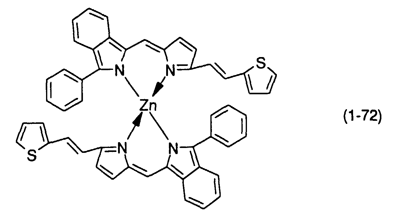
- It was confirmed on the basis of the following analytical results that the thus obtained compound was the desired compound.
Elemental analysis (C50H34N4S2Zn) C H N S Calcd. (%) 73.21 4.18 6.83 7.82 Found (%) 73.36 4.22 6.77 7.95 - MS (m/e): 820 (M+)
-
- The thus obtained compound showed a maximum absorption at 597 nm in a toluene solution and had a Gram absorbancy index of 1.72×10⁵ ml/g.cm.
Claims (10)
- An optical recording medium having at least a recording layer and a reflective layer on a substrate, wherein at least one dipyrromethene metal chelate compound represented by formula (1) is contained in the recording layer:wherein R1 and R9 are each independently an alkenyl group, an aryl group or a heteroaryl group; R2 to R8 are each independently a hydrogen atom, a halogen atom, or a substituted or unsubstituted alkyl, alkoxy, alkenyl, acyl, alkoxycarbonyl, aralkyl, aryl or heteroaryl group having 20 or less carbon atoms; and M is a transition metal.
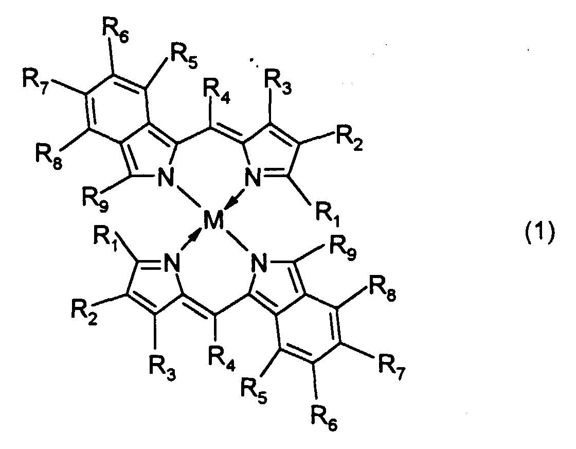
- The optical recording medium according to Claim 1 wherein R1 in formula (1) is -CH=CH-R10, wherein R10 is a hydrogen atom, a halogen atom, or a substituted or unsubstituted alkyl, alkoxy, alkenyl, acyl, alkoxycarbonyl, aralkyl, aryl or heteroaryl group having 20 or less carbon atoms.
- The optical recording medium according to Claim 1 wherein R1 in formula (1) is a substituted or unsubstituted aryl or heteroaryl group having 20 or less carbon atoms, and M is copper or cobalt.
- The optical recording medium according to Claim 3 wherein R1 and R3 in formula (1) are simultaneously substituted or unsubstituted aryl or heteroaryl groups having 20 or less carbon atoms.
- The optical recording medium according to Claim 4 wherein R1, R3 and R9 in formula (1) are substituted or unsubstituted aryl groups having 20 or less carbon atoms, and at least one of the aryl groups is substituted by a halogen, or at least one of R2, R4 to R8 is a halogen atom.
- The optical recording medium according to any one of Claims 1 to 5 wherein the recording layer further includes at least one other dipyrromethene metal chelate compound represented by formula (2):wherein R11 to R17 are each independently a hydrogen atom, a halogen atom, a nitro group, a cyano group, a hydroxyl group, an amino group, a carboxyl group, a sulfonic acid group, or a substituted or unsubstituted alkyl, alkoxy, alkylthio, aryloxy, arylthio, alkenyl, acyl, alkoxycarbonyl, carbamoyl, acylamino, aralkyl, aryl or heteroaryl group having 20 or less carbon atoms, and R15 and R16 may be bonded to each other to form an aromatic ring which may have a substituent; and M' is a transition element.
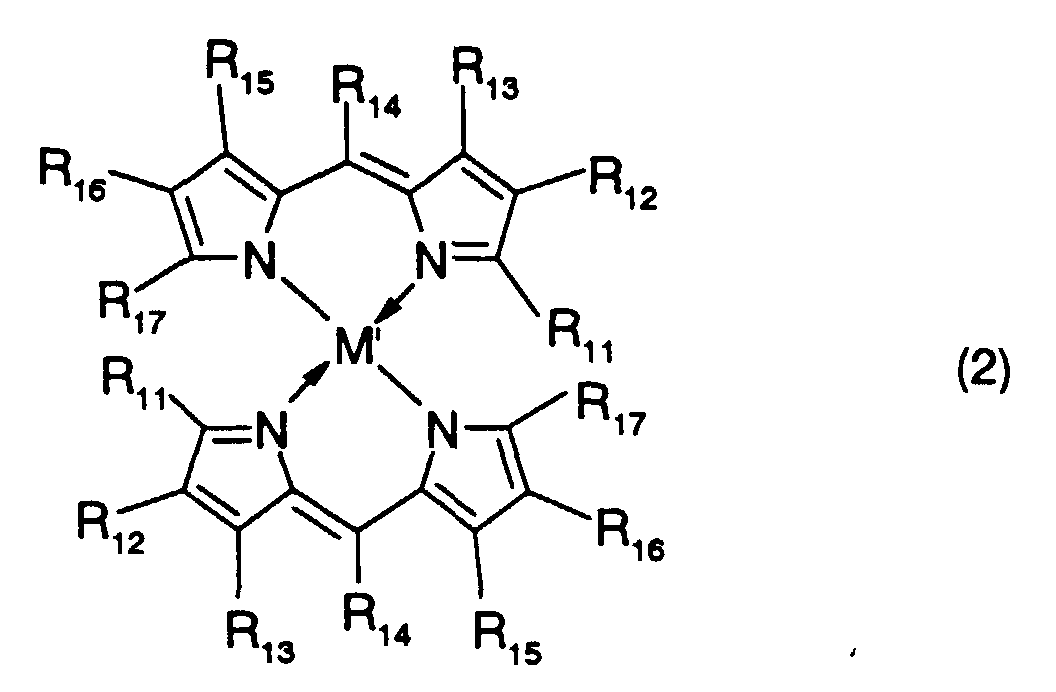
- The optical recording medium according to Claim 6 wherein the other dipyrromethene metal chelate compound is selected from compounds represented by formula (3):wherein R19 to R25 are each independently a hydrogen atom, a halogen atom, a nitro group, a cyano group, a hydroxyl group, an amino group, a carboxyl group, a sulfonic acid group, or a substituted or unsubstituted alkyl, alkoxy, alkylthio, aryloxy, arylthio, alkenyl, acyl, alkoxycarbonyl, carbamoyl, acylamino or aralkyl group having 20 or less carbon atoms; R18 and R26 are each independently an alkenyl group or an aryl group having 20 or less carbon atoms; and M'' is copper or cobalt.

- The optical recording medium according to any one of Claims 1 to 7 wherein at a laser wavelength of 520 to 690 nm, a refractive index and an extinction coefficient of the recording layer are 1.8 or more and 0.04 to 0.40, respectively.
- The optical recording medium according to any one of Claims 1 to 7 which is recordable and reproducible by a laser beam selected within the wavelength range of 520 to 690 nm.
- A dipyrromethene metal chelate compound represented by formula (4):wherein R27 to R35 are each independently a hydrogen atom, a halogen atom, or a substituted or unsubstituted alkyl, alkoxy, alkenyl, acyl, alkoxycarbonyl, aralkyl, aryl or heteroaryl group having 20 or less carbon atoms; and M''' is a transition element.

Applications Claiming Priority (15)
| Application Number | Priority Date | Filing Date | Title |
|---|---|---|---|
| JP25201097 | 1997-09-17 | ||
| JP9252010A JPH1192682A (en) | 1997-09-17 | 1997-09-17 | Dipyrromethene metal chelate compound and optical recording medium using the same |
| JP252010/97 | 1997-09-17 | ||
| JP33444697 | 1997-12-04 | ||
| JP334446/97 | 1997-12-04 | ||
| JP33444697A JP3656884B2 (en) | 1997-12-04 | 1997-12-04 | Optical recording medium |
| JP03290998A JP3740565B2 (en) | 1998-02-16 | 1998-02-16 | Optical recording medium |
| JP32908/98 | 1998-02-16 | ||
| JP3290898 | 1998-02-16 | ||
| JP32909/98 | 1998-02-16 | ||
| JP03290898A JP3740564B2 (en) | 1998-02-16 | 1998-02-16 | Optical recording medium |
| JP3290998 | 1998-02-16 | ||
| JP13673698 | 1998-05-19 | ||
| JP136736/98 | 1998-05-19 | ||
| JP13673698A JP3742507B2 (en) | 1998-05-19 | 1998-05-19 | Optical recording medium |
Publications (3)
| Publication Number | Publication Date |
|---|---|
| EP0903733A2 true EP0903733A2 (en) | 1999-03-24 |
| EP0903733A3 EP0903733A3 (en) | 1999-04-21 |
| EP0903733B1 EP0903733B1 (en) | 2004-12-08 |
Family
ID=27521463
Family Applications (1)
| Application Number | Title | Priority Date | Filing Date |
|---|---|---|---|
| EP98117641A Expired - Fee Related EP0903733B1 (en) | 1997-09-17 | 1998-09-17 | Optical recording medium and dipyrromethene metal chelate compound for use therein |
Country Status (5)
| Country | Link |
|---|---|
| US (2) | US6162520A (en) |
| EP (1) | EP0903733B1 (en) |
| KR (1) | KR100274132B1 (en) |
| CN (1) | CN1174398C (en) |
| DE (1) | DE69828008T2 (en) |
Cited By (6)
| Publication number | Priority date | Publication date | Assignee | Title |
|---|---|---|---|---|
| EP1130584A2 (en) * | 2000-02-28 | 2001-09-05 | Mitsui Chemicals, Inc. | Dipyrromethene-metal chelate compound and optical recording medium using thereof |
| EP1245571A1 (en) * | 2000-01-07 | 2002-10-02 | Mitsui Chemicals, Inc. | Benzbisazole compound and optical recording medium containing the compound |
| WO2003082593A1 (en) * | 2002-03-29 | 2003-10-09 | Mitsui Chemicals, Inc. | Optical recording media and dipyrromethene-metal chelate compounds |
| EP1750263A2 (en) * | 2005-07-29 | 2007-02-07 | Kabushiki Kaisha Toshiba | Information storage medium, and reproducing method and recording method therefor |
| US7425553B2 (en) | 2003-05-30 | 2008-09-16 | Gemin X Pharmaceuticals Canada Inc. | Triheterocyclic compounds, compositions, and methods for treating cancer or viral diseases |
| US7625621B2 (en) | 2004-07-29 | 2009-12-01 | Clariant Finance (Bvi) Limited | Amino antipyrine based azo ligands and their metal complexes for use as optical recording media |
Families Citing this family (3)
| Publication number | Priority date | Publication date | Assignee | Title |
|---|---|---|---|---|
| US20060159882A1 (en) * | 2003-03-03 | 2006-07-20 | Urs Lehmann | Optical recording materials having high storage density |
| US20070184232A1 (en) * | 2004-02-23 | 2007-08-09 | Ryuichi Takahashi | Optical recording materials having high storage density |
| CN101001923A (en) * | 2004-08-10 | 2007-07-18 | 西巴特殊化学品控股有限公司 | Optical recording materials having high storage density |
Citations (3)
| Publication number | Priority date | Publication date | Assignee | Title |
|---|---|---|---|---|
| US5433896A (en) * | 1994-05-20 | 1995-07-18 | Molecular Probes, Inc. | Dibenzopyrrometheneboron difluoride dyes |
| JPH09131968A (en) * | 1995-11-08 | 1997-05-20 | Tdk Corp | Optical recording medium |
| EP0822544A1 (en) * | 1996-07-29 | 1998-02-04 | Mitsui Toatsu Chemicals, Incorporated | Optical recording medium |
Family Cites Families (17)
| Publication number | Priority date | Publication date | Assignee | Title |
|---|---|---|---|---|
| JPH0474690A (en) * | 1990-07-17 | 1992-03-10 | Ricoh Co Ltd | Optical information recording medium |
| JPH0538878A (en) * | 1991-08-07 | 1993-02-19 | Nippon Columbia Co Ltd | Light recording medium |
| JPH0640162A (en) * | 1992-01-22 | 1994-02-15 | Nippon Columbia Co Ltd | Optical recording medium |
| JPH0640161A (en) * | 1992-01-22 | 1994-02-15 | Nippon Columbia Co Ltd | Optical recording medium |
| JP2865955B2 (en) * | 1992-09-09 | 1999-03-08 | 日本コロムビア株式会社 | Optical recording medium |
| JPH06199045A (en) * | 1993-01-08 | 1994-07-19 | Pioneer Electron Corp | Photo recording medium |
| JPH0776169A (en) * | 1993-06-18 | 1995-03-20 | Ricoh Co Ltd | Optical information record medium |
| JP3500474B2 (en) * | 1993-09-09 | 2004-02-23 | 株式会社リコー | Optical information recording medium |
| JPH07262604A (en) * | 1994-03-25 | 1995-10-13 | Mitsui Toatsu Chem Inc | Optical recording medium |
| JP3731244B2 (en) * | 1996-04-03 | 2006-01-05 | 三菱化学株式会社 | Optical recording medium and manufacturing method thereof |
| JPH09156218A (en) * | 1995-12-08 | 1997-06-17 | Mitsubishi Chem Corp | Optical recording medium and data recording method |
| JPH09193544A (en) * | 1996-01-17 | 1997-07-29 | Mitsubishi Chem Corp | Optical recording medium and data recording method |
| JPH09194748A (en) * | 1996-01-17 | 1997-07-29 | Mitsubishi Chem Corp | Optical recording medium and information recording method |
| JP3648823B2 (en) * | 1996-01-18 | 2005-05-18 | 三菱化学株式会社 | Optical recording medium and information recording method |
| JP3572774B2 (en) * | 1996-01-19 | 2004-10-06 | 三菱化学株式会社 | Optical recording medium and information recording method |
| JP3632094B2 (en) * | 1996-01-25 | 2005-03-23 | 株式会社リコー | Optical information recording medium |
| JPH09267562A (en) * | 1996-01-29 | 1997-10-14 | Ricoh Co Ltd | Optical recording medium |
-
1998
- 1998-09-08 US US09/149,027 patent/US6162520A/en not_active Expired - Fee Related
- 1998-09-17 DE DE69828008T patent/DE69828008T2/en not_active Expired - Fee Related
- 1998-09-17 KR KR1019980038373A patent/KR100274132B1/en not_active IP Right Cessation
- 1998-09-17 EP EP98117641A patent/EP0903733B1/en not_active Expired - Fee Related
- 1998-09-17 CN CNB981246559A patent/CN1174398C/en not_active Expired - Fee Related
-
2000
- 2000-10-06 US US09/685,647 patent/US6355327B1/en not_active Expired - Fee Related
Patent Citations (3)
| Publication number | Priority date | Publication date | Assignee | Title |
|---|---|---|---|---|
| US5433896A (en) * | 1994-05-20 | 1995-07-18 | Molecular Probes, Inc. | Dibenzopyrrometheneboron difluoride dyes |
| JPH09131968A (en) * | 1995-11-08 | 1997-05-20 | Tdk Corp | Optical recording medium |
| EP0822544A1 (en) * | 1996-07-29 | 1998-02-04 | Mitsui Toatsu Chemicals, Incorporated | Optical recording medium |
Non-Patent Citations (1)
| Title |
|---|
| PATENT ABSTRACTS OF JAPAN vol. 097, no. 009, 30 September 1997 & JP 09 131968 A (TDK CORP), 20 May 1997 * |
Cited By (12)
| Publication number | Priority date | Publication date | Assignee | Title |
|---|---|---|---|---|
| EP1245571A1 (en) * | 2000-01-07 | 2002-10-02 | Mitsui Chemicals, Inc. | Benzbisazole compound and optical recording medium containing the compound |
| EP1245571A4 (en) * | 2000-01-07 | 2003-09-17 | Mitsui Chemicals Inc | Benzbisazole compound and optical recording medium containing the compound |
| EP1130584A2 (en) * | 2000-02-28 | 2001-09-05 | Mitsui Chemicals, Inc. | Dipyrromethene-metal chelate compound and optical recording medium using thereof |
| EP1130584A3 (en) * | 2000-02-28 | 2002-05-08 | Mitsui Chemicals, Inc. | Dipyrromethene-metal chelate compound and optical recording medium using thereof |
| US6479123B2 (en) | 2000-02-28 | 2002-11-12 | Mitsui Chemicals, Inc. | Dipyrromethene-metal chelate compound and optical recording medium using thereof |
| WO2003082593A1 (en) * | 2002-03-29 | 2003-10-09 | Mitsui Chemicals, Inc. | Optical recording media and dipyrromethene-metal chelate compounds |
| US7425553B2 (en) | 2003-05-30 | 2008-09-16 | Gemin X Pharmaceuticals Canada Inc. | Triheterocyclic compounds, compositions, and methods for treating cancer or viral diseases |
| US7709477B2 (en) | 2003-05-30 | 2010-05-04 | Gemin X Pharmaceuticals Canada Inc. | Methods for treating cancer |
| US8420638B2 (en) | 2003-05-30 | 2013-04-16 | Gemin X Pharmaceuticals Canada Inc. | Triheterocyclic compounds and compositions thereof |
| US7625621B2 (en) | 2004-07-29 | 2009-12-01 | Clariant Finance (Bvi) Limited | Amino antipyrine based azo ligands and their metal complexes for use as optical recording media |
| EP1750263A2 (en) * | 2005-07-29 | 2007-02-07 | Kabushiki Kaisha Toshiba | Information storage medium, and reproducing method and recording method therefor |
| EP1750263A3 (en) * | 2005-07-29 | 2009-07-01 | Kabushiki Kaisha Toshiba | Information storage medium, and reproducing method and recording method therefor |
Also Published As
| Publication number | Publication date |
|---|---|
| DE69828008T2 (en) | 2005-06-02 |
| US6355327B1 (en) | 2002-03-12 |
| KR100274132B1 (en) | 2001-01-15 |
| DE69828008D1 (en) | 2005-01-13 |
| EP0903733A3 (en) | 1999-04-21 |
| KR19990029872A (en) | 1999-04-26 |
| CN1218257A (en) | 1999-06-02 |
| US6162520A (en) | 2000-12-19 |
| CN1174398C (en) | 2004-11-03 |
| EP0903733B1 (en) | 2004-12-08 |
Similar Documents
| Publication | Publication Date | Title |
|---|---|---|
| EP0822544B1 (en) | Optical recording medium | |
| JP3708298B2 (en) | Optical recording medium | |
| JP3614586B2 (en) | Dipyromethene metal chelate compound and optical recording medium using the same | |
| EP0903733A2 (en) | Optical recording medium and dipyrromethene metal chelate compound for use therein | |
| JPH1192479A (en) | Optical recording medium | |
| KR100445137B1 (en) | Dipyrromethene-metal chelate compound and optical recording medium using thereof | |
| JPH11256057A (en) | Dipyrromethene-metal chelate compound and optical recording medium containing the same | |
| JP3868099B2 (en) | Dibenzopyromethene boron chelate compound and optical recording medium comprising the same | |
| JPH11256056A (en) | Benzopyrromethene-metal chelate compound and optical recording medium containing the sane | |
| JPH1143491A (en) | Pyrromethene metallic chelate compound and optical recording medium using the same | |
| JP3740565B2 (en) | Optical recording medium | |
| JPH1192682A (en) | Dipyrromethene metal chelate compound and optical recording medium using the same | |
| JP3656884B2 (en) | Optical recording medium | |
| JP3742507B2 (en) | Optical recording medium | |
| JPH10287819A (en) | Benzopyrromethene-based compound and optical recording medium using the same | |
| JPH11302551A (en) | Dipyrromethene metal chelate compound and photorecording medium containing the same | |
| JP3742487B2 (en) | Optical recording medium | |
| JPH11302253A (en) | Dipyrromethene metal chelate compound and optically recording medium using the same | |
| JP3740564B2 (en) | Optical recording medium | |
| JP2004314327A (en) | Optical recording medium | |
| JP3790112B2 (en) | Dipyromethene metal chelate compound and optical recording medium using the same | |
| JP2004314326A (en) | Optical recording medium | |
| JP2002155076A (en) | Diprromethene metal chelate compound and photorecording medium using the same | |
| JP2005054106A (en) | Dipyrromethene metal chelate compound and optical recording medium produced by using the same | |
| JP2003064274A (en) | Dipyrromethene metal chelate compound and light recording medium using the same |
Legal Events
| Date | Code | Title | Description |
|---|---|---|---|
| PUAI | Public reference made under article 153(3) epc to a published international application that has entered the european phase |
Free format text: ORIGINAL CODE: 0009012 |
|
| PUAL | Search report despatched |
Free format text: ORIGINAL CODE: 0009013 |
|
| 17P | Request for examination filed |
Effective date: 19980917 |
|
| AK | Designated contracting states |
Kind code of ref document: A2 Designated state(s): DE FR GB NL |
|
| AX | Request for extension of the european patent |
Free format text: AL;LT;LV;MK;RO;SI |
|
| AK | Designated contracting states |
Kind code of ref document: A3 Designated state(s): AT BE CH CY DE DK ES FI FR GB GR IE IT LI LU MC NL PT SE |
|
| AX | Request for extension of the european patent |
Free format text: AL;LT;LV;MK;RO;SI |
|
| AKX | Designation fees paid |
Free format text: DE FR GB NL |
|
| 17Q | First examination report despatched |
Effective date: 20001107 |
|
| GRAP | Despatch of communication of intention to grant a patent |
Free format text: ORIGINAL CODE: EPIDOSNIGR1 |
|
| GRAS | Grant fee paid |
Free format text: ORIGINAL CODE: EPIDOSNIGR3 |
|
| GRAA | (expected) grant |
Free format text: ORIGINAL CODE: 0009210 |
|
| RAP1 | Party data changed (applicant data changed or rights of an application transferred) |
Owner name: YAMAMOTO CHEMICALS, INC. Owner name: MITSUI CHEMICALS, INC. |
|
| AK | Designated contracting states |
Kind code of ref document: B1 Designated state(s): DE FR GB NL |
|
| REG | Reference to a national code |
Ref country code: GB Ref legal event code: FG4D |
|
| REF | Corresponds to: |
Ref document number: 69828008 Country of ref document: DE Date of ref document: 20050113 Kind code of ref document: P |
|
| PG25 | Lapsed in a contracting state [announced via postgrant information from national office to epo] |
Ref country code: GB Free format text: LAPSE BECAUSE OF NON-PAYMENT OF DUE FEES Effective date: 20050917 |
|
| PLBE | No opposition filed within time limit |
Free format text: ORIGINAL CODE: 0009261 |
|
| STAA | Information on the status of an ep patent application or granted ep patent |
Free format text: STATUS: NO OPPOSITION FILED WITHIN TIME LIMIT |
|
| ET | Fr: translation filed | ||
| 26N | No opposition filed |
Effective date: 20050909 |
|
| PG25 | Lapsed in a contracting state [announced via postgrant information from national office to epo] |
Ref country code: NL Free format text: LAPSE BECAUSE OF NON-PAYMENT OF DUE FEES Effective date: 20060401 Ref country code: DE Free format text: LAPSE BECAUSE OF NON-PAYMENT OF DUE FEES Effective date: 20060401 |
|
| GBPC | Gb: european patent ceased through non-payment of renewal fee |
Effective date: 20050917 |
|
| PG25 | Lapsed in a contracting state [announced via postgrant information from national office to epo] |
Ref country code: FR Free format text: LAPSE BECAUSE OF NON-PAYMENT OF DUE FEES Effective date: 20060531 |
|
| NLV4 | Nl: lapsed or anulled due to non-payment of the annual fee |
Effective date: 20060401 |
|
| REG | Reference to a national code |
Ref country code: FR Ref legal event code: ST Effective date: 20060531 |