EP0923080A2 - Burst length discriminating circuit for use in synchronous semiconductor memory with burst mode - Google Patents
Burst length discriminating circuit for use in synchronous semiconductor memory with burst mode Download PDFInfo
- Publication number
- EP0923080A2 EP0923080A2 EP98123435A EP98123435A EP0923080A2 EP 0923080 A2 EP0923080 A2 EP 0923080A2 EP 98123435 A EP98123435 A EP 98123435A EP 98123435 A EP98123435 A EP 98123435A EP 0923080 A2 EP0923080 A2 EP 0923080A2
- Authority
- EP
- European Patent Office
- Prior art keywords
- burst length
- signal
- output
- holding means
- discriminating circuit
- Prior art date
- Legal status (The legal status is an assumption and is not a legal conclusion. Google has not performed a legal analysis and makes no representation as to the accuracy of the status listed.)
- Granted
Links
Images


Classifications
-
- G—PHYSICS
- G11—INFORMATION STORAGE
- G11C—STATIC STORES
- G11C11/00—Digital stores characterised by the use of particular electric or magnetic storage elements; Storage elements therefor
- G11C11/21—Digital stores characterised by the use of particular electric or magnetic storage elements; Storage elements therefor using electric elements
- G11C11/34—Digital stores characterised by the use of particular electric or magnetic storage elements; Storage elements therefor using electric elements using semiconductor devices
- G11C11/40—Digital stores characterised by the use of particular electric or magnetic storage elements; Storage elements therefor using electric elements using semiconductor devices using transistors
- G11C11/401—Digital stores characterised by the use of particular electric or magnetic storage elements; Storage elements therefor using electric elements using semiconductor devices using transistors forming cells needing refreshing or charge regeneration, i.e. dynamic cells
- G11C11/4063—Auxiliary circuits, e.g. for addressing, decoding, driving, writing, sensing or timing
- G11C11/407—Auxiliary circuits, e.g. for addressing, decoding, driving, writing, sensing or timing for memory cells of the field-effect type
-
- G—PHYSICS
- G11—INFORMATION STORAGE
- G11C—STATIC STORES
- G11C7/00—Arrangements for writing information into, or reading information out from, a digital store
- G11C7/10—Input/output [I/O] data interface arrangements, e.g. I/O data control circuits, I/O data buffers
- G11C7/1015—Read-write modes for single port memories, i.e. having either a random port or a serial port
- G11C7/1018—Serial bit line access mode, e.g. using bit line address shift registers, bit line address counters, bit line burst counters
Definitions
- the present invention relates to a semiconductor memory, and more specifically to a burst length discriminating circuit for use in a synchronous semiconductor memory with a burst mode.
- a mode discriminating circuit 100 receives various control signals including at least a row address strobe signal RAS, and a column address strobe signal CAS, and an internal address (only one address signal IA11 of which is shown in Fig. 4), and outputs various mode signals labeled "MODE FLAGS".
- the mode discriminating circuit 100 is initialized by a power-on-reset signal PON supplied to a reset input of the mode discriminating circuit 10.
- the inputted signals are held in D-latches (not shown) during a high level period of an internal clock CLK which is brought to a high level during a predetermined period of time from a rising of an external clock.
- Outputs of the D-latches (not shown) are connected to a decoder (not shown) so that the outputs of the D-latches are converted by action of the decoder into a mode signal in accordance with a combination of the inputted signals.
- Each mode signal is held in a D-latch until a rising of a next internal clock CLK.
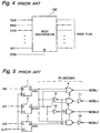
- Fig. 5 there is shown a logic circuit diagram of a burst length discriminating circuit included in the prior art semiconductor memory circuit having the burst mode.
- Fig. 6 is a truth table of a decoder section of the burst length discriminating circuit
- Fig. 7 is a truth table of the burst length discriminating circuit.
- the shown prior art burst length discriminating circuit includes three D-latches (D-type flipflops) 1, 2 and 3, and a decoder 20 which are constituted of a two-input NOR gate 4, a two-input NAND gate 5, a three-input NOR gate 6, a three-input NAND gate 7 and four inverters 9, 10, 11 and 12, connected as shown.
- the D-latches (D-type flipflops) 1, 2 and 3 latch three least significant address bits "IA0", “IA1” and “IA2" of the address, in synchronism with a rising of the internal clock CLK in a mode register set cycle, and hold the latched address bits "IA0", “IA1” and “IA2” until the rising of the next the internal clock CLK.
- the decoder 20 selectively activates a burst length discrimination signal on the basis of the logical combination of the address bits "IA0", “IA1” and “IA2".
- the relation between the burst lengths and the address signals corresponding to key address signals is defined in JEDEC as shown in Fig. 7. Therefore, when all of the address bits "IA0", “IA1” and “IA2" are at a high level, the burst length discrimination signal MDBLF indicating the full page burst is activated.
- the decoder 20 is configured to realize the truth table shown in Fig. 6.
- the truth table of the burst length discriminating circuit is the same as that of the decoder included in the burst length discriminating circuit, and therefore, the latches provided in the burst length discriminating circuit supply the decoder with the address signals having the same polarity as those supplied to the burst length discriminating circuit.
- initial conditions of the D-latches and sequential circuits are indefinite. Therefore, the D-latches and sequential circuits are initialized by the power-in-reset signal PON (internal initializing signal) at the power-on time, so that the semiconductor memory circuit becomes an expected predetermined internal condition.
- PON internal initializing signal
- a bus check in order to check whether or not a semiconductor memory circuit exists on the memory bus, is carried out by monitoring a minute current flowing when a voltage is applied to the memory bus.
- the burst length selected by the burst length discriminating circuit is any of the burst lengths "1", “2", “4" and "8", after the data corresponding to the designated burst length is outputted in synchronism with an external clock, the input/output pins are brought into the high impedance condition. Therefore, no substantial problem occurs.
- the input/output pins are maintained in a data outputting condition until a burst stop command, a precharge command or a write command (excluding the case that a CAS latency is "3") is inputted. Namely, since the data continues to be outputted in synchronism with the external clock, a large current disadvantageously flows at the bus checking of the system.
- a memory check is carried out just after a power-on time, in order to check whether or not the semiconductor memory existing on the memory bus operates normally, by executing a reading and writing of data.
- the plurality of semiconductor memories are checked one by one in the order. In this case, not only the output pins of the semiconductor memory to be checked but also the output pins of the semiconductor memories not to be checked are connected to the same memory bus.
- Another object of the present invention is to provide a burst length discriminating circuit for use in a synchronous semiconductor memory with a burst mode, which can never select the burst length of the full page even if the semiconductor memory is not properly initialized at a power-on time.
- a burst length discriminating circuit for use in a synchronous semiconductor memory with a burst mode, comprising:
- each of the plurality of holding means holds respective input signals in synchronism with a clock signal.
- each of the plurality of holding means comprises a D-type flipflop having a data input connected to receive a corresponding input signal and a clock input connected to receive the clock signal.
- the decoding means includes a plurality of logic circuits so connected to selectively activate the burst length discrimination signal determined by the combination of logical values of the address signals, and to activate the burst length discrimination signal indicating the burst length other than the full page when the outputs of all the plurality of holding means are at the same logical level.
- the burst length discriminating circuit receives the three least significant address signals of an address, and the plurality of holding means comprising three holding means for receiving the three least significant address signals, respectively, and wherein the at least one inverting means receives one of the three least significant address signals to output an inverted signal to a corresponding one of the three holding means.
- the decoding means receives output of the three holding means, and activates a burst length discrimination signal indicating the burst length 8 when all outputs of the three holding means are at the same logical level at the power-on time.
- the at least one inverting means receives the most significant address signal of the three least significant address signals to output an inverted signal to the corresponding one of the three holding means.
- the at least one inverting means includes an inverter receiving the most significant address signal of the three least significant address signals to output an inverted address signal.
- the three holding means includes a first D-type flipflop having a data input connected to latch and hold the least significant address signal of the three least significant address signals in response to a clock signal, a second D-type flipflop having a data input connected to latch and hold the second least significant address signal of the three least significant address signals in response to the clock signal, and a third D-type flipflop having a data input connected to latch and hold the inverted address signal in response to clock signal.
- the decoding means includes a two-input NOR circuit receiving an output of the first D-type flipflop and an output of the second D-type flipflop for outputting a first burst length discrimination signal, a two-input AND circuit receiving an inverted signal of the output of the first D-type flipflop and the output of the second D-type flipflop for outputting a second burst length discrimination signal, a three-input AND circuit receiving the output of the first D-type flipflop, the output of the second D-type flipflop and an output of the third D-type flipflop, for outputting a third burst length discrimination signal, and a three-input NOR circuit receiving the inverted signal of the output of the first D-type flipflop, the inverted signal of the output of the second D-type flipflop and an output of the third D-type flipflop, for outputting a fourth burst length discrimination signal indicating the full page.
- Fig. 1 there is shown a logic circuit diagram of the burst length discriminating circuit in an embodiment of the semiconductor memory circuit in accordance with the present invention having a full page burst write/read function.
- elements corresponding to those shown in Fig. 5 are given the same Reference Numerals.
- the shown burst length discriminating circuit includes three D-latches (D-type flipflops) 1, 2 and 3, an inverter 8, and a decoder 20 which are constituted of a two-input NOR gate 4, a two-input NAND gate 5, a three-input NOR gate 6, a three-input NAND gate 7 and four inverters 9, 10, 11 and 12, connected as shown.
- the shown burst length discriminating circuit has the same circuit construction as that of the burst prior art length discriminating circuit shown in Fig. 5, excepting that the inverter 8 is inserted before the input of the latch 3 receiving the key address signal IA2.
- the shown burst length discriminating circuit receives internal address signals "IA0", “IA1” and “IA2” corresponding to the three least significant bits “A0", “A1” and “A2” of an external address (not shown), respectively. Therefore, the internal address signals "IA0", “IA1” and “IA2” are key address signals for the burst length discriminating circuit, and supplied to a data input "D" of the D-latch 1, a data input "D" of the D-latch 2, and an input of the inverter 8, respectively. An output of the inverter 8 is connected to a data input "D" of the D-latch 3.
- a clock input "D" of each of the three D-latches 1, 2 and 3 is connected to receive an internal clock CLK in phase with an external clock (not shown) so that each of D-latches 1, 2 and 3 latches the corresponding input address signal in response to a rising of the internal clock CLK in a mode register set cycle, and holds the latched address signal until the rising of the next internal clock CLK.
- the three D-latches 1, 2 and 3 have the same circuit construction and are constructed with the same mask pattern.
- Output of the three D-latches 1, 2 and 3 are supplied to the decoder 20. Specifically, an output "IA0Q" of the D-latch 1 is connected to a first input of the two-input NOR gate 4, an input of the inverter 9 and a first input of the three-input NAND gate 7. An output "IA1Q” of the D-latch 2 is connected to a second input of the two-input NOR gate 4, a first input of the two-input NAND gate 5, an input of the inverter 10 and a second input of the three-input NAND gate 7.
- a output "IA2Q" of the D-latch 3 is connected to a first input of the three-input NOR gate 6 and a third input of the three-input NAND gate 7.
- An output of the inverter 9 is connected to a second input of the two-input NAND gate 5 and a second input of the three-input NOR gate 6.
- An output of the inverter 10 is connected to a third input of the three-input NOR gate 6.
- An output of the two-input NOR gate 4 outputs a first burst length discrimination signal "MDBL1", which is brought to a high level when the burst length is 1 bit.
- An output of the two-input NAND gate 5 is connected to an input of the inverter 11, and an output of the inverter 11 outputs a second burst length discrimination signal "MDBL4", which is brought to a high level when the burst length is 4 bits.
- An output of the three-input NAND gate 7 is connected to an input of the inverter 12, and an output of the inverter 12 outputs a third burst length discrimination signal "MDBL8", which is brought to a high level when the burst length is 8 bits.
- An output of the three-input NOR gate 6 outputs a fourth burst length discrimination signal "MDBLF", which is brought to a high level when the burst length is the full page.
- a two-input AND circuit is constituted of the two-input NAND gate 5 and the inverter 11
- a three-input AND gate circuit is constituted of the three-input NAND gate 7 and the inverter 12.
- FIG. 2 there is shown a truth table of the decoder 20 receiving the outputs "IA0Q”, “IA1Q” and “IA2Q" of the three D-latches 1, 2 and 3.
- Fig. 3 there is shown a truth table of the burst length discriminating circuit shown in Fig. 1.
- the truth table of the burst length discriminating circuit shown in Fig. 3 is the same as the truth table of the burst length discriminating circuit shown in Fig. 7, provided in the prior art semiconductor memory circuit having the burst mode. Therefore, in a situation excluding the power-on time, the burst length discriminating circuit shown in Fig. 1 operates similarly to the burst length discriminating circuit provided in the prior art semiconductor memory circuit having the burst mode.
- the shown embodiment of the burst length discriminating circuit of the semiconductor memory circuit having the burst mode is characterized in that at least one of the D-latches latching the key address signals supplied to the burst length discriminating circuit is connected to receive through one inverter the corresponding key address signal, contrary to the prior art ordinary sense in which the latch (flipflop) is connected to output an internal signal having the same polarity as that of an external signal externally supplied to the latch.
- two or more of the key address signals supplied to the burst length discriminating circuit can be supplied through inverters to the corresponding latches, if all of the key address signals supplied to the burst length discriminating circuit are not supplied through inverters.
- the decoder receiving the output of the latches is so modified to have a logic construction which never changes the logical relation between the key address signal and the output of the burst length discriminating circuit.
- the decoder shown in Fig. 1 is the same in logic circuit construction as that of the decoder of the prior art burst length discriminating circuit, but that the burst length discrimination signal "MDBL8" and the burst length discrimination signal "MDBLF" are exchanged. Therefore, the shown embodiment can advantageously realize the present invention with a minimum modification of the prior art circuit.
- the burst length other than the full page is selected. Accordingly, even if the semiconductor memory circuit in accordance with the present invention having the burst mode is put in a read mode at the power-on time, the burst length other than the full page is selected, so that, after information corresponding to the burst length (8 bits at maximum) is outputted in synchronism with the external clock, the output pins are brought into a high impedance condition, and therefore, the semiconductor memory circuit becomes a condition ready to receive an input signal. Thus, inconvenience does not occur at a memory checking time or at a bus checking time in a personal computer or a word station.
- the synchronous semiconductor memory circuit in accordance with the present invention having the burst mode is featured in that the burst length discriminating circuit has a plurality of latches for latching and holding a corresponding number of key address signals, at least one inverter receiving one key address signal of the key address signals for supplying an inverted key address signal to a corresponding latch of the plurality of latches, and a decoder receiving outputs of the plurality of latches for selectively activating one of burst length discrimination signals, so that when all of inputs of the decoder are at the high level or at the low level, the decoder activates the burst length discrimination signal indicating the burst length other than the full page.
- the burst length other than the full page is selected. Accordingly, when information corresponding to the burst length has been outputted in synchronism with the external clock supplied after the power-on, the output pins are brought into a high impedance condition until the bus checking is conducted. Therefore, even if a voltage is supplied from the system, since the output pins are in the high impedance condition, no large current flows. Thus, in the bus check just after the power-on in the system such as a personal computer or a word station, there does not occur such inconvenience that a large current flows because the output pins are in a condition continuing to output the data.
- the output pins are in the high impedance condition, a write data supplied from the system is never destroyed. Therefore, in the high speed system such as the personal computer or the word station having a plurality of synchronous semiconductor memory circuits having the burst mode, connected to a common memory bus, in parallel to one another, the write data supplied from the system to the semiconductor memory circuit under test, is never destroyed by an output data from another semiconductor memory circuit connected to the memory bus to which the semiconductor memory circuit under test is connected. Accordingly, the inconvenience at the memory checking is prevented.
Abstract
Description
- The present invention relates to a semiconductor memory, and more specifically to a burst length discriminating circuit for use in a synchronous semiconductor memory with a burst mode.
- In the prior art, a synchronous semiconductor memory circuit having a burst mode has been known.
- In the prior art semiconductor memory circuit having the burst mode, as shown in Fig. 4, a mode
discriminating circuit 100 receives various control signals including at least a row address strobe signal RAS, and a column address strobe signal CAS, and an internal address (only one address signal IA11 of which is shown in Fig. 4), and outputs various mode signals labeled "MODE FLAGS". The modediscriminating circuit 100 is initialized by a power-on-reset signal PON supplied to a reset input of the modediscriminating circuit 10. - The inputted signals are held in D-latches (not shown) during a high level period of an internal clock CLK which is brought to a high level during a predetermined period of time from a rising of an external clock. Outputs of the D-latches (not shown) are connected to a decoder (not shown) so that the outputs of the D-latches are converted by action of the decoder into a mode signal in accordance with a combination of the inputted signals. Each mode signal is held in a D-latch until a rising of a next internal clock CLK.
- Referring to Fig. 5, there is shown a logic circuit diagram of a burst length discriminating circuit included in the prior art semiconductor memory circuit having the burst mode. Fig. 6 is a truth table of a decoder section of the burst length discriminating circuit, and Fig. 7 is a truth table of the burst length discriminating circuit.
- The shown prior art burst length discriminating circuit includes three D-latches (D-type flipflops) 1, 2 and 3, and a
decoder 20 which are constituted of a two-input NOR gate 4, a two-input NAND gate 5, a three-input NOR gate 6, a three-input NAND gate 7 and fourinverters - The
decoder 20 selectively activates a burst length discrimination signal on the basis of the logical combination of the address bits "IA0", "IA1" and "IA2". The relation between the burst lengths and the address signals corresponding to key address signals is defined in JEDEC as shown in Fig. 7. Therefore, when all of the address bits "IA0", "IA1" and "IA2" are at a high level, the burst length discrimination signal MDBLF indicating the full page burst is activated. In order to realize the truth table shown in Fig. 7, thedecoder 20 is configured to realize the truth table shown in Fig. 6. Namely, the truth table of the burst length discriminating circuit is the same as that of the decoder included in the burst length discriminating circuit, and therefore, the latches provided in the burst length discriminating circuit supply the decoder with the address signals having the same polarity as those supplied to the burst length discriminating circuit. - At a power-on time, initial conditions of the D-latches and sequential circuits (not shown) are indefinite. Therefore, the D-latches and sequential circuits are initialized by the power-in-reset signal PON (internal initializing signal) at the power-on time, so that the semiconductor memory circuit becomes an expected predetermined internal condition.
- In general, in a system such a personal computer or a work station, if a voltage is applied to an input/output pin of the semiconductor memory circuit, a minute current flows in an input protection circuit provided in the input/output pin. By utilizing this feature, just after the power-on, a bus check in order to check whether or not a semiconductor memory circuit exists on the memory bus, is carried out by monitoring a minute current flowing when a voltage is applied to the memory bus.
- In the system having the prior art semiconductor memory circuit having the burst mode, on the other hand, if the power-in-reset signal were not generated for any reason at the power-on time, the internal condition is not initialized, and the system hardly returns to a normal condition. As a result, if the input/output pin of the semiconductor memory circuit is in a condition of outputting the data, a large current flows, and therefore, the bus check cannot be performed.
- Specifically, since the initial conditions of the D-latches and sequential circuits are indefinite at the power-on time, various internal nodes which were at the ground level at the power-on time elevate with elevation of the power supply voltage, each various internal node finally becomes either the low level or the high level to which the internal node is apt to shift because of variation of an individual circuit element in a manufacturing process. As a result, the semiconductor memory circuit becomes an unexpected internal condition. However, even if the initialization result in failure, if a mode erroneously selected by the mode discriminator was a mode register setting mode, a refresh mode, or a write mode, the input/output pins are put in a high impedance condition, and therefore, no large current disadvantageously flows at the bus checking of the system.
- In addition, even if the erroneously selected mode was a read mode, if the burst length selected by the burst length discriminating circuit is any of the burst lengths "1", "2", "4" and "8", after the data corresponding to the designated burst length is outputted in synchronism with an external clock, the input/output pins are brought into the high impedance condition. Therefore, no substantial problem occurs.
- However, if the erroneously selected mode is the read mode, and if the burst length selected by the burst length discriminating circuit is the full page (full page burst read mode), the input/output pins are maintained in a data outputting condition until a burst stop command, a precharge command or a write command (excluding the case that a CAS latency is "3") is inputted. Namely, since the data continues to be outputted in synchronism with the external clock, a large current disadvantageously flows at the bus checking of the system.
- Here, considering the burst length discriminating circuit, all the D-latches included in the burst length discriminating circuit have the same circuit construction and formed in the same mask pattern. Therefore, at the power-on time, outputs of all the D-latches included in the burst length discriminating circuit are apt to become the same logical level which either a high level or a low level.
- Since the input-output relation of the decoder in order to cause the burst length discriminating circuit to meet with the relation between the key address signals and the burst lengths defined in JEDEC as shown in Fig. 7, is as shown in Fig. 6, when all the inputs of the decoder are at a high level, the full page is selected as the burst length.
- In addition, in a system such as a personal computer or a work station, a memory check is carried out just after a power-on time, in order to check whether or not the semiconductor memory existing on the memory bus operates normally, by executing a reading and writing of data. In a high speed system having a plurality of semiconductor memories having the burst mode, connected to the memory bus, in parallel to one another, the plurality of semiconductor memories are checked one by one in the order. In this case, not only the output pins of the semiconductor memory to be checked but also the output pins of the semiconductor memories not to be checked are connected to the same memory bus. Therefore, if the output pins of at least one of the semiconductor memories not to be checked are in the data outputting condition (namely, in the full page burst read mode) (because the semiconductor memory was not properly initialized at the power-on time), the data supplied from the system is destroyed, and therefore, the data supplied from the system is not properly written into the semiconductor memory to be checked, with the result that the result of the memory checking becomes error.
- Accordingly, it is an object of the present invention to provide a burst length discriminating circuit for use in a synchronous semiconductor memory with a burst mode which has overcome the above mentioned defect of the conventional one.
- Another object of the present invention is to provide a burst length discriminating circuit for use in a synchronous semiconductor memory with a burst mode, which can never select the burst length of the full page even if the semiconductor memory is not properly initialized at a power-on time.
- The above and other objects of the present invention are achieved in accordance with the present invention by a burst length discriminating circuit for use in a synchronous semiconductor memory with a burst mode, comprising:
- a plurality of holding means for latching and holding a corresponding number of address signals;
- at least one inverting means receiving one address signal of the address signals for supplying an inverted address signal to a corresponding holding means of the holding means; and
- a decoding means receiving outputs of the plurality of holding means for selectively activating a burst length discrimination signal determined by a combination of logical values of the address signals, the decoding means activating a burst length discrimination signal indicating a burst length other than a full page when the outputs of all the plurality of holding means are at the same logical level.
-
- In an embodiment of the burst length discriminating circuit, the plurality of holding means hold respective input signals in synchronism with a clock signal. Specifically, each of the plurality of holding means comprises a D-type flipflop having a data input connected to receive a corresponding input signal and a clock input connected to receive the clock signal.
- Furthermore, the decoding means includes a plurality of logic circuits so connected to selectively activate the burst length discrimination signal determined by the combination of logical values of the address signals, and to activate the burst length discrimination signal indicating the burst length other than the full page when the outputs of all the plurality of holding means are at the same logical level.
- In a preferred embodiment, the burst length discriminating circuit receives the three least significant address signals of an address, and the plurality of holding means comprising three holding means for receiving the three least significant address signals, respectively, and wherein the at least one inverting means receives one of the three least significant address signals to output an inverted signal to a corresponding one of the three holding means. The decoding means receives output of the three holding means, and activates a burst length discrimination signal indicating the
burst length 8 when all outputs of the three holding means are at the same logical level at the power-on time. The at least one inverting means receives the most significant address signal of the three least significant address signals to output an inverted signal to the corresponding one of the three holding means. - In a specific preferred embodiment, the at least one inverting means includes an inverter receiving the most significant address signal of the three least significant address signals to output an inverted address signal. The three holding means includes a first D-type flipflop having a data input connected to latch and hold the least significant address signal of the three least significant address signals in response to a clock signal, a second D-type flipflop having a data input connected to latch and hold the second least significant address signal of the three least significant address signals in response to the clock signal, and a third D-type flipflop having a data input connected to latch and hold the inverted address signal in response to clock signal. The decoding means includes a two-input NOR circuit receiving an output of the first D-type flipflop and an output of the second D-type flipflop for outputting a first burst length discrimination signal, a two-input AND circuit receiving an inverted signal of the output of the first D-type flipflop and the output of the second D-type flipflop for outputting a second burst length discrimination signal, a three-input AND circuit receiving the output of the first D-type flipflop, the output of the second D-type flipflop and an output of the third D-type flipflop, for outputting a third burst length discrimination signal, and a three-input NOR circuit receiving the inverted signal of the output of the first D-type flipflop, the inverted signal of the output of the second D-type flipflop and an output of the third D-type flipflop, for outputting a fourth burst length discrimination signal indicating the full page.
- The above and other objects, features and advantages of the present invention will be apparent from the following description of preferred embodiments of the invention with reference to the accompanying drawings.
-
- Fig. 1 is a logic circuit diagram of the burst length discriminating circuit in an embodiment of the semiconductor memory circuit in accordance with the present invention having a burst mode;
- Fig. 2 is a truth table of a decoder section of the burst length discriminating circuit shown in Fig. 1;
- Fig. 3 is a truth table of the burst length discriminating circuit shown in Fig. 1;
- Fig. 4 illustrates inputs and outputs of the mode discriminating circuit in the prior art semiconductor memory circuit having a burst mode;
- Fig. 5 is a logic circuit diagram of the burst length discriminating circuit in the prior art semiconductor memory circuit having the burst mode;
- Fig. 6 is a truth table of a decoder section of the burst length discriminating circuit shown in Fig. 5; and
- Fig. 7 is a truth table of the burst length discriminating circuit shown in Fig. 5.
-
- Referring to Fig. 1, there is shown a logic circuit diagram of the burst length discriminating circuit in an embodiment of the semiconductor memory circuit in accordance with the present invention having a full page burst write/read function. In Fig. 1, elements corresponding to those shown in Fig. 5 are given the same Reference Numerals.
- The shown burst length discriminating circuit includes three D-latches (D-type flipflops) 1, 2 and 3, an
inverter 8, and adecoder 20 which are constituted of a two-input NORgate 4, a two-input NAND gate 5, a three-input NOR gate 6, a three-input NAND gate 7 and fourinverters inverter 8 is inserted before the input of thelatch 3 receiving the key address signal IA2. - More specifically, the shown burst length discriminating circuit receives internal address signals "IA0", "IA1" and "IA2" corresponding to the three least significant bits "A0", "A1" and "A2" of an external address (not shown), respectively. Therefore, the internal address signals "IA0", "IA1" and "IA2" are key address signals for the burst length discriminating circuit, and supplied to a data input "D" of the D-
latch 1, a data input "D" of the D-latch 2, and an input of theinverter 8, respectively. An output of theinverter 8 is connected to a data input "D" of the D-latch 3. A clock input "D" of each of the three D-latches latches latches - Output of the three D-
latches decoder 20. Specifically, an output "IA0Q" of the D-latch 1 is connected to a first input of the two-input NORgate 4, an input of theinverter 9 and a first input of the three-input NAND gate 7. An output "IA1Q" of the D-latch 2 is connected to a second input of the two-input NORgate 4, a first input of the two-input NAND gate 5, an input of theinverter 10 and a second input of the three-input NAND gate 7. A output "IA2Q" of the D-latch 3 is connected to a first input of the three-input NOR gate 6 and a third input of the three-input NAND gate 7. An output of theinverter 9 is connected to a second input of the two-input NAND gate 5 and a second input of the three-input NOR gate 6. An output of theinverter 10 is connected to a third input of the three-input NOR gate 6. - An output of the two-input NOR
gate 4 outputs a first burst length discrimination signal "MDBL1", which is brought to a high level when the burst length is 1 bit. An output of the two-input NAND gate 5 is connected to an input of theinverter 11, and an output of theinverter 11 outputs a second burst length discrimination signal "MDBL4", which is brought to a high level when the burst length is 4 bits. An output of the three-input NAND gate 7 is connected to an input of theinverter 12, and an output of theinverter 12 outputs a third burst length discrimination signal "MDBL8", which is brought to a high level when the burst length is 8 bits. An output of the three-input NOR gate 6 outputs a fourth burst length discrimination signal "MDBLF", which is brought to a high level when the burst length is the full page. In the above construction, a two-input AND circuit is constituted of the two-input NAND gate 5 and theinverter 11, and a three-input AND gate circuit is constituted of the three-input NAND gate 7 and theinverter 12. - Referring to Fig. 2, there is shown a truth table of the
decoder 20 receiving the outputs "IA0Q", "IA1Q" and "IA2Q" of the three D-latches - As seen from the truth table of Fig. 2, even if all the outputs of the D-
latches - Referring to Fig. 3, there is shown a truth table of the burst length discriminating circuit shown in Fig. 1. As seen from comparison between Fig. 3 and Fig. 7, the truth table of the burst length discriminating circuit shown in Fig. 3 is the same as the truth table of the burst length discriminating circuit shown in Fig. 7, provided in the prior art semiconductor memory circuit having the burst mode. Therefore, in a situation excluding the power-on time, the burst length discriminating circuit shown in Fig. 1 operates similarly to the burst length discriminating circuit provided in the prior art semiconductor memory circuit having the burst mode.
- As seen from the above, the shown embodiment of the burst length discriminating circuit of the semiconductor memory circuit having the burst mode is characterized in that at least one of the D-latches latching the key address signals supplied to the burst length discriminating circuit is connected to receive through one inverter the corresponding key address signal, contrary to the prior art ordinary sense in which the latch (flipflop) is connected to output an internal signal having the same polarity as that of an external signal externally supplied to the latch. Here, of course, two or more of the key address signals supplied to the burst length discriminating circuit can be supplied through inverters to the corresponding latches, if all of the key address signals supplied to the burst length discriminating circuit are not supplied through inverters. On the other hand, since at least one of the key address signals supplied to the burst length discriminating circuit is supplied through an inverter to the corresponding latch, the decoder receiving the output of the latches is so modified to have a logic construction which never changes the logical relation between the key address signal and the output of the burst length discriminating circuit. In the shown embodiment, however, the decoder shown in Fig. 1 is the same in logic circuit construction as that of the decoder of the prior art burst length discriminating circuit, but that the burst length discrimination signal "MDBL8" and the burst length discrimination signal "MDBLF" are exchanged. Therefore, the shown embodiment can advantageously realize the present invention with a minimum modification of the prior art circuit.
- Thus, even if all the latches receiving the key address signals in the burst length discriminating circuit output the high level signal or the low level signal at the power-on time, the burst length other than the full page is selected. Accordingly, even if the semiconductor memory circuit in accordance with the present invention having the burst mode is put in a read mode at the power-on time, the burst length other than the full page is selected, so that, after information corresponding to the burst length (8 bits at maximum) is outputted in synchronism with the external clock, the output pins are brought into a high impedance condition, and therefore, the semiconductor memory circuit becomes a condition ready to receive an input signal. Thus, inconvenience does not occur at a memory checking time or at a bus checking time in a personal computer or a word station.
- As seen from the above, the synchronous semiconductor memory circuit in accordance with the present invention having the burst mode is featured in that the burst length discriminating circuit has a plurality of latches for latching and holding a corresponding number of key address signals, at least one inverter receiving one key address signal of the key address signals for supplying an inverted key address signal to a corresponding latch of the plurality of latches, and a decoder receiving outputs of the plurality of latches for selectively activating one of burst length discrimination signals, so that when all of inputs of the decoder are at the high level or at the low level, the decoder activates the burst length discrimination signal indicating the burst length other than the full page.
- With this arrangement, even if a read mode is erroneously selected at the power-on time, the burst length other than the full page is selected. Accordingly, when information corresponding to the burst length has been outputted in synchronism with the external clock supplied after the power-on, the output pins are brought into a high impedance condition until the bus checking is conducted. Therefore, even if a voltage is supplied from the system, since the output pins are in the high impedance condition, no large current flows. Thus, in the bus check just after the power-on in the system such as a personal computer or a word station, there does not occur such inconvenience that a large current flows because the output pins are in a condition continuing to output the data.
- Furthermore, since the output pins are in the high impedance condition, a write data supplied from the system is never destroyed. Therefore, in the high speed system such as the personal computer or the word station having a plurality of synchronous semiconductor memory circuits having the burst mode, connected to a common memory bus, in parallel to one another, the write data supplied from the system to the semiconductor memory circuit under test, is never destroyed by an output data from another semiconductor memory circuit connected to the memory bus to which the semiconductor memory circuit under test is connected. Accordingly, the inconvenience at the memory checking is prevented.
- The invention has thus been shown and described with reference to the specific embodiments. However, it should be noted that the present invention is in no way limited to the details of the illustrated structures but changes and modifications may be made within the scope of the appended claims.
Claims (8)
- A burst length discriminating circuit for use in a synchronous semiconductor memory with a burst mode, comprising:a plurality of holding means for latching and holding a corresponding number of address signals;at least one inverting means receiving one address signal of said address signals for supplying an inverted address signal to a corresponding holding means of said holding means; anda decoding means receiving outputs of said plurality of holding means for selectively activating a burst length discrimination signal determined by a combination of logical values of said address signals, said decoding means activating a burst length discrimination signal indicating a burst length other than a full page when said outputs of all said plurality of holding means are at the same logical level.
- A burst length discriminating circuit claimed in Claim 1 wherein said plurality of holding means hold respective input signals in synchronism with a clock signal.
- A burst length discriminating circuit claimed in Claim 2 wherein each of said plurality of holding means comprises a D-type flipflop having a data input connected to receive a corresponding input signal and a clock input connected to receive said clock signal.
- A burst length discriminating circuit claimed in Claim 1 wherein said decoding means includes a plurality of logic circuits so connected to selectively activate the burst length discrimination signal determined by the combination of logical values of said address signals, and to activate the burst length discrimination signal indicating the burst length other than the full page when said outputs of all said plurality of holding means are at the same logical level.
- A burst length discriminating circuit claimed in Claim 1 wherein the burst length discriminating circuit receives the three least significant address signals of an address, and said plurality of holding means comprising three holding means for receiving said three least significant address signals, respectively, and wherein said at least one inverting means receives one of said three least significant address signals to output an inverted signal to a corresponding one of said three holding means.
- A burst length discriminating circuit claimed in Claim 5 wherein said decoding means receives output of said three holding means, and activates a burst length discrimination signal indicating the burst length 8 when all outputs of said three holding means are at the same logical level at the power-on time.
- A burst length discriminating circuit claimed in Claim 6 wherein said at least one inverting means receives the most significant address signal of said three least significant address signals to output an inverted signal to the corresponding one of said three holding means.
- A burst length discriminating circuit claimed in Claim 5 wherein said at least one inverting means includes an inverter receiving the most significant address signal of said three least significant address signals to output an inverted address signal;
wherein said three holding means includes a first D-type flipflop having a data input connected to latch and hold the least significant address signal of said three least significant address signals in response to a clock signal, a second D-type flipflop having a data input connected to latch and hold the second least significant address signal of said three least significant address signals in response to said clock signal, and a third D-type flipflop having a data input connected to latch and hold said inverted address signal in response to clock signal; and
wherein said decoding means includes a two-input NOR circuit receiving an output of said first D-type flipflop and an output of said second D-type flipflop for outputting a first burst length discrimination signal, a two-input AND circuit receiving an inverted signal of said output of said first D-type flipflop and said output of said second D-type flipflop for outputting a second burst length discrimination signal, a three-input AND circuit receiving said output of said first D-type flipflop, said output of said second D-type flipflop and an output of said third D-type flipflop, for outputting a third burst length discrimination signal, and a three-input NOR circuit receiving said inverted signal of said output of said first D-type flipflop, said inverted signal of said output of said second D-type flipflop and an output of said third D-type flipflop, for outputting a fourth burst length discrimination signal indicating the full page.
Applications Claiming Priority (2)
| Application Number | Priority Date | Filing Date | Title |
|---|---|---|---|
| JP33981897 | 1997-12-10 | ||
| JP33981897A JP3204384B2 (en) | 1997-12-10 | 1997-12-10 | Semiconductor memory circuit |
Publications (3)
| Publication Number | Publication Date |
|---|---|
| EP0923080A2 true EP0923080A2 (en) | 1999-06-16 |
| EP0923080A3 EP0923080A3 (en) | 1999-11-17 |
| EP0923080B1 EP0923080B1 (en) | 2001-05-16 |
Family
ID=18331117
Family Applications (1)
| Application Number | Title | Priority Date | Filing Date |
|---|---|---|---|
| EP98123435A Expired - Lifetime EP0923080B1 (en) | 1997-12-10 | 1998-12-09 | Burst length discriminating circuit for use in synchronous semiconductor memory and having a predetermined initialized state of power-up |
Country Status (6)
| Country | Link |
|---|---|
| US (1) | US6347356B2 (en) |
| EP (1) | EP0923080B1 (en) |
| JP (1) | JP3204384B2 (en) |
| KR (1) | KR100288994B1 (en) |
| CN (1) | CN1130728C (en) |
| DE (1) | DE69800791T2 (en) |
Families Citing this family (3)
| Publication number | Priority date | Publication date | Assignee | Title |
|---|---|---|---|---|
| US6557090B2 (en) * | 2001-03-09 | 2003-04-29 | Micron Technology, Inc. | Column address path circuit and method for memory devices having a burst access mode |
| KR100597635B1 (en) * | 2004-05-20 | 2006-07-05 | 삼성전자주식회사 | Internal reset signal generator for use in semiconductor memory |
| KR100625293B1 (en) * | 2004-06-30 | 2006-09-20 | 주식회사 하이닉스반도체 | Semiconductor memory devict with high reliability and operation method there for |
Citations (3)
| Publication number | Priority date | Publication date | Assignee | Title |
|---|---|---|---|---|
| EP0618585A2 (en) * | 1993-04-02 | 1994-10-05 | Nec Corporation | Semiconductor memory device synchronous with external clock signal for outputting data bits through a small number of data lines |
| US5526320A (en) * | 1994-12-23 | 1996-06-11 | Micron Technology Inc. | Burst EDO memory device |
| US5659515A (en) * | 1994-10-31 | 1997-08-19 | Mitsubishi Denki Kabushiki Kaisha | Semiconductor memory device capable of refresh operation in burst mode |
Family Cites Families (11)
| Publication number | Priority date | Publication date | Assignee | Title |
|---|---|---|---|---|
| DE69120483T2 (en) * | 1990-08-17 | 1996-11-14 | Sgs Thomson Microelectronics | Semiconductor memory with suppressed test mode input during power on |
| US6175901B1 (en) * | 1994-04-15 | 2001-01-16 | Micron Technology, Inc. | Method for initializing and reprogramming a control operation feature of a memory device |
| KR0171942B1 (en) * | 1995-06-30 | 1999-03-30 | 김주용 | Burst length detection circuit |
| JP2991094B2 (en) * | 1995-09-19 | 1999-12-20 | 日本電気株式会社 | Semiconductor storage device |
| JPH09251773A (en) | 1996-03-13 | 1997-09-22 | Hitachi Ltd | Semiconductor storage device |
| JP3351953B2 (en) * | 1996-03-19 | 2002-12-03 | 富士通株式会社 | Mode register control circuit and semiconductor device having the same |
| KR100218734B1 (en) * | 1996-05-06 | 1999-09-01 | 김영환 | Internal pulse generating method and circuit of synchronous memory |
| JP3919847B2 (en) * | 1996-05-29 | 2007-05-30 | 三菱電機株式会社 | Semiconductor memory device |
| JP2848339B2 (en) * | 1996-06-14 | 1999-01-20 | 日本電気株式会社 | Redundant decode circuit |
| WO1998013828A1 (en) * | 1996-09-26 | 1998-04-02 | Mitsubishi Denki Kabushiki Kaisha | Synchronous type semiconductor memory device |
| JPH1139871A (en) * | 1997-01-10 | 1999-02-12 | Mitsubishi Electric Corp | Synchronous semiconductor storage device |
-
1997
- 1997-12-10 JP JP33981897A patent/JP3204384B2/en not_active Expired - Fee Related
-
1998
- 1998-12-09 EP EP98123435A patent/EP0923080B1/en not_active Expired - Lifetime
- 1998-12-09 US US09/207,619 patent/US6347356B2/en not_active Expired - Lifetime
- 1998-12-09 DE DE69800791T patent/DE69800791T2/en not_active Expired - Lifetime
- 1998-12-10 KR KR1019980054254A patent/KR100288994B1/en not_active IP Right Cessation
- 1998-12-10 CN CN98125203A patent/CN1130728C/en not_active Expired - Fee Related
Patent Citations (3)
| Publication number | Priority date | Publication date | Assignee | Title |
|---|---|---|---|---|
| EP0618585A2 (en) * | 1993-04-02 | 1994-10-05 | Nec Corporation | Semiconductor memory device synchronous with external clock signal for outputting data bits through a small number of data lines |
| US5659515A (en) * | 1994-10-31 | 1997-08-19 | Mitsubishi Denki Kabushiki Kaisha | Semiconductor memory device capable of refresh operation in burst mode |
| US5526320A (en) * | 1994-12-23 | 1996-06-11 | Micron Technology Inc. | Burst EDO memory device |
Also Published As
| Publication number | Publication date |
|---|---|
| CN1130728C (en) | 2003-12-10 |
| EP0923080A3 (en) | 1999-11-17 |
| DE69800791T2 (en) | 2002-04-18 |
| DE69800791D1 (en) | 2001-06-21 |
| EP0923080B1 (en) | 2001-05-16 |
| US20020004879A1 (en) | 2002-01-10 |
| KR100288994B1 (en) | 2001-07-12 |
| CN1219739A (en) | 1999-06-16 |
| JPH11176157A (en) | 1999-07-02 |
| KR19990062967A (en) | 1999-07-26 |
| JP3204384B2 (en) | 2001-09-04 |
| US6347356B2 (en) | 2002-02-12 |
Similar Documents
| Publication | Publication Date | Title |
|---|---|---|
| US4882709A (en) | Conditional write RAM | |
| JP3167359B2 (en) | Semiconductor memory having multi-clock operation for test mode entry | |
| US6536004B2 (en) | On-chip circuit and method for testing memory devices | |
| KR100282974B1 (en) | A synchronous semiconductor device having a circuit capable of reliably resetting a test mode. | |
| US7872511B2 (en) | Circuit and method for initializing an internal logic unit in a semiconductor memory device | |
| US5831931A (en) | Address strobe recognition in a memory device | |
| US7050353B2 (en) | Semiconductor memory having burst transfer function | |
| JP3467053B2 (en) | Method and apparatus for detecting an address transition to a write state machine interface circuit for flash memory | |
| JP3331481B2 (en) | Test circuit for semiconductor device | |
| JPH05288806A (en) | Semiconductor memory having sequential clock type access code for test mode entry | |
| KR100324150B1 (en) | Memory address generator circuit and semiconductor memory device | |
| JP2000149600A (en) | Semiconductor storage device | |
| US6975547B2 (en) | Flash memory devices that support efficient memory locking operations and methods of operating flash memory devices | |
| EP1915502A2 (en) | Memory device with a data hold latch | |
| JP3221887B2 (en) | Semiconductor memory having chip enable control from output enable during test mode | |
| CN1716444B (en) | Semiconductor memory device capable of stably setting mode register set and method therefor | |
| JPH05312926A (en) | Semiconductor memory having flag displaying test mode | |
| EP0923080B1 (en) | Burst length discriminating circuit for use in synchronous semiconductor memory and having a predetermined initialized state of power-up | |
| US10566074B2 (en) | Test mode control circuit | |
| KR0167869B1 (en) | Dynamic semiconductor memory | |
| KR100211483B1 (en) | Semiconductor memory using block writing system | |
| JPS6117077B2 (en) | ||
| JPH05189296A (en) | Simultaneous writing access device for single-bit memory | |
| JPS6314440B2 (en) | ||
| JPS63278156A (en) | Memory writing control circuit |
Legal Events
| Date | Code | Title | Description |
|---|---|---|---|
| PUAI | Public reference made under article 153(3) epc to a published international application that has entered the european phase |
Free format text: ORIGINAL CODE: 0009012 |
|
| AK | Designated contracting states |
Kind code of ref document: A2 Designated state(s): DE FR GB |
|
| AX | Request for extension of the european patent |
Free format text: AL;LT;LV;MK;RO;SI |
|
| PUAL | Search report despatched |
Free format text: ORIGINAL CODE: 0009013 |
|
| AK | Designated contracting states |
Kind code of ref document: A3 Designated state(s): AT BE CH CY DE DK ES FI FR GB GR IE IT LI LU MC NL PT SE |
|
| AX | Request for extension of the european patent |
Free format text: AL;LT;LV;MK;RO;SI |
|
| 17P | Request for examination filed |
Effective date: 19991209 |
|
| AKX | Designation fees paid |
Free format text: DE FR GB |
|
| GRAG | Despatch of communication of intention to grant |
Free format text: ORIGINAL CODE: EPIDOS AGRA |
|
| 17Q | First examination report despatched |
Effective date: 20000802 |
|
| GRAG | Despatch of communication of intention to grant |
Free format text: ORIGINAL CODE: EPIDOS AGRA |
|
| GRAG | Despatch of communication of intention to grant |
Free format text: ORIGINAL CODE: EPIDOS AGRA |
|
| GRAH | Despatch of communication of intention to grant a patent |
Free format text: ORIGINAL CODE: EPIDOS IGRA |
|
| RTI1 | Title (correction) |
Free format text: BURST LENGTH DISCRIMINATING CIRCUIT FOR USE IN SYNCHRONOUS SEMICONDUCTOR MEMORY AND HAVING A PREDETERMINED INITIALIZED STATE OF POWER-UP |
|
| GRAH | Despatch of communication of intention to grant a patent |
Free format text: ORIGINAL CODE: EPIDOS IGRA |
|
| GRAA | (expected) grant |
Free format text: ORIGINAL CODE: 0009210 |
|
| AK | Designated contracting states |
Kind code of ref document: B1 Designated state(s): DE FR GB |
|
| REF | Corresponds to: |
Ref document number: 69800791 Country of ref document: DE Date of ref document: 20010621 |
|
| ET | Fr: translation filed | ||
| REG | Reference to a national code |
Ref country code: GB Ref legal event code: IF02 |
|
| PLBE | No opposition filed within time limit |
Free format text: ORIGINAL CODE: 0009261 |
|
| STAA | Information on the status of an ep patent application or granted ep patent |
Free format text: STATUS: NO OPPOSITION FILED WITHIN TIME LIMIT |
|
| 26N | No opposition filed | ||
| REG | Reference to a national code |
Ref country code: GB Ref legal event code: 732E |
|
| REG | Reference to a national code |
Ref country code: FR Ref legal event code: TQ |
|
| REG | Reference to a national code |
Ref country code: GB Ref legal event code: 732E |
|
| REG | Reference to a national code |
Ref country code: FR Ref legal event code: TP |
|
| PGFP | Annual fee paid to national office [announced via postgrant information from national office to epo] |
Ref country code: GB Payment date: 20091209 Year of fee payment: 12 |
|
| GBPC | Gb: european patent ceased through non-payment of renewal fee |
Effective date: 20101209 |
|
| PG25 | Lapsed in a contracting state [announced via postgrant information from national office to epo] |
Ref country code: GB Free format text: LAPSE BECAUSE OF NON-PAYMENT OF DUE FEES Effective date: 20101209 |
|
| PGFP | Annual fee paid to national office [announced via postgrant information from national office to epo] |
Ref country code: DE Payment date: 20131204 Year of fee payment: 16 |
|
| PGFP | Annual fee paid to national office [announced via postgrant information from national office to epo] |
Ref country code: FR Payment date: 20131209 Year of fee payment: 16 |
|
| REG | Reference to a national code |
Ref country code: FR Ref legal event code: TP Owner name: PS4 LUXCO S.A.R.L., LU Effective date: 20141014 |
|
| REG | Reference to a national code |
Ref country code: DE Ref legal event code: R119 Ref document number: 69800791 Country of ref document: DE |
|
| REG | Reference to a national code |
Ref country code: FR Ref legal event code: ST Effective date: 20150831 |
|
| PG25 | Lapsed in a contracting state [announced via postgrant information from national office to epo] |
Ref country code: DE Free format text: LAPSE BECAUSE OF NON-PAYMENT OF DUE FEES Effective date: 20150701 |
|
| PG25 | Lapsed in a contracting state [announced via postgrant information from national office to epo] |
Ref country code: FR Free format text: LAPSE BECAUSE OF NON-PAYMENT OF DUE FEES Effective date: 20141231 |