EP0929104A2 - Electroluminescence device and process for producing the same - Google Patents
Electroluminescence device and process for producing the same Download PDFInfo
- Publication number
- EP0929104A2 EP0929104A2 EP99100080A EP99100080A EP0929104A2 EP 0929104 A2 EP0929104 A2 EP 0929104A2 EP 99100080 A EP99100080 A EP 99100080A EP 99100080 A EP99100080 A EP 99100080A EP 0929104 A2 EP0929104 A2 EP 0929104A2
- Authority
- EP
- European Patent Office
- Prior art keywords
- electroluminescence device
- layer
- hole
- emission
- organic
- Prior art date
- Legal status (The legal status is an assumption and is not a legal conclusion. Google has not performed a legal analysis and makes no representation as to the accuracy of the status listed.)
- Granted
Links
Images


Classifications
-
- H—ELECTRICITY
- H10—SEMICONDUCTOR DEVICES; ELECTRIC SOLID-STATE DEVICES NOT OTHERWISE PROVIDED FOR
- H10K—ORGANIC ELECTRIC SOLID-STATE DEVICES
- H10K50/00—Organic light-emitting devices
- H10K50/10—OLEDs or polymer light-emitting diodes [PLED]
- H10K50/11—OLEDs or polymer light-emitting diodes [PLED] characterised by the electroluminescent [EL] layers
- H10K50/125—OLEDs or polymer light-emitting diodes [PLED] characterised by the electroluminescent [EL] layers specially adapted for multicolour light emission, e.g. for emitting white light
-
- H—ELECTRICITY
- H10—SEMICONDUCTOR DEVICES; ELECTRIC SOLID-STATE DEVICES NOT OTHERWISE PROVIDED FOR
- H10K—ORGANIC ELECTRIC SOLID-STATE DEVICES
- H10K85/00—Organic materials used in the body or electrodes of devices covered by this subclass
- H10K85/60—Organic compounds having low molecular weight
- H10K85/615—Polycyclic condensed aromatic hydrocarbons, e.g. anthracene
-
- H—ELECTRICITY
- H10—SEMICONDUCTOR DEVICES; ELECTRIC SOLID-STATE DEVICES NOT OTHERWISE PROVIDED FOR
- H10K—ORGANIC ELECTRIC SOLID-STATE DEVICES
- H10K85/00—Organic materials used in the body or electrodes of devices covered by this subclass
- H10K85/60—Organic compounds having low molecular weight
- H10K85/631—Amine compounds having at least two aryl rest on at least one amine-nitrogen atom, e.g. triphenylamine
-
- H—ELECTRICITY
- H10—SEMICONDUCTOR DEVICES; ELECTRIC SOLID-STATE DEVICES NOT OTHERWISE PROVIDED FOR
- H10K—ORGANIC ELECTRIC SOLID-STATE DEVICES
- H10K85/00—Organic materials used in the body or electrodes of devices covered by this subclass
- H10K85/60—Organic compounds having low molecular weight
- H10K85/649—Aromatic compounds comprising a hetero atom
- H10K85/657—Polycyclic condensed heteroaromatic hydrocarbons
- H10K85/6572—Polycyclic condensed heteroaromatic hydrocarbons comprising only nitrogen in the heteroaromatic polycondensed ring system, e.g. phenanthroline or carbazole
-
- H—ELECTRICITY
- H10—SEMICONDUCTOR DEVICES; ELECTRIC SOLID-STATE DEVICES NOT OTHERWISE PROVIDED FOR
- H10K—ORGANIC ELECTRIC SOLID-STATE DEVICES
- H10K2102/00—Constructional details relating to the organic devices covered by this subclass
- H10K2102/10—Transparent electrodes, e.g. using graphene
- H10K2102/101—Transparent electrodes, e.g. using graphene comprising transparent conductive oxides [TCO]
- H10K2102/103—Transparent electrodes, e.g. using graphene comprising transparent conductive oxides [TCO] comprising indium oxides, e.g. ITO
-
- H—ELECTRICITY
- H10—SEMICONDUCTOR DEVICES; ELECTRIC SOLID-STATE DEVICES NOT OTHERWISE PROVIDED FOR
- H10K—ORGANIC ELECTRIC SOLID-STATE DEVICES
- H10K85/00—Organic materials used in the body or electrodes of devices covered by this subclass
- H10K85/30—Coordination compounds
- H10K85/321—Metal complexes comprising a group IIIA element, e.g. Tris (8-hydroxyquinoline) gallium [Gaq3]
- H10K85/324—Metal complexes comprising a group IIIA element, e.g. Tris (8-hydroxyquinoline) gallium [Gaq3] comprising aluminium, e.g. Alq3
-
- Y—GENERAL TAGGING OF NEW TECHNOLOGICAL DEVELOPMENTS; GENERAL TAGGING OF CROSS-SECTIONAL TECHNOLOGIES SPANNING OVER SEVERAL SECTIONS OF THE IPC; TECHNICAL SUBJECTS COVERED BY FORMER USPC CROSS-REFERENCE ART COLLECTIONS [XRACs] AND DIGESTS
- Y10—TECHNICAL SUBJECTS COVERED BY FORMER USPC
- Y10S—TECHNICAL SUBJECTS COVERED BY FORMER USPC CROSS-REFERENCE ART COLLECTIONS [XRACs] AND DIGESTS
- Y10S428/00—Stock material or miscellaneous articles
- Y10S428/917—Electroluminescent
Definitions
- a transparent electrode, an organic layer (particularly, the organic hole transfer layer, the hole block layer and the organic electron transfer layer), and a metallic electrode are laminated in this order on an optically transparent substrate.
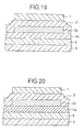
- Fig. 20 is a schematic cross sectional view showing an important part of a blue emission element 21B in a sixth embodiment according to the second aspect of the invention.
- BSB-BCN (having the formula (17)) was vapor deposited (vapor deposition rate: from 0.2 to 0.4 nm/sec) on the transparent electrode 5 as an electron transfer red emission material layer 32 at a thickness of 20 nm in the stripe pattern of 1.15 mm x 48.0 mm, which was an emission region of the ITO electrode 5, with changing to a mask 22c having 12 openings 23c having a stripe form having an area of 1.16 mm x 49 mm.
- Alq 3 (8-hydorxy quinoline aluminum having the formula (18)) was vapor deposited at a thickness of 40 nm as an electron transfer layer or an electron transfer emission layer 2.
- the specific constitution of the organic EL device 21 of this example is explained based on its production process.
- DMC2 (having the formula (19)) and Alq 3 (8-hydorxy quinoline aluminum having the formula (18)) was vapor deposited (vapor deposition rate: from 0.2 to 0.4 nm/sec) in such a manner that the molar ratio of DCM2 was from 0.5 to 1% on the transparent electrode 5 as an electron transfer red emission material layer 32 at a thickness of 20 nm in the stripe pattern of 1.15 mm x 48.0 mm, which was an emission region of the ITO electrode 5, with changing to a mask 22c having 12 openings 23c having a stripe form having an area of 1.16 mm x 49 mm.
- the organic EL device according to Example 3 of the invention is explained based on its production process.
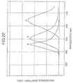
- Fig. 22 is a graph showing the spectral characteristics of the organic EL device according to Example 3 shown in Fig. 11.
- the luminance was 1,400 cd/m 2 at a current density of 400 mA/cm 2 .
- the current did substantially not flow until a voltage of about 5 V, which gradually began to flow exceeding 5 V, and it suddenly flew exceeding 6 V. This means that it can be driven with a low voltage, and its threshold value voltage characteristics are good.
- the organic EL device according to Example 4 of the invention is explained based on its production process.
- the hole transfer layer can serve as an emission layer due to sufficient electron-hole recombination in the hole transfer layer by providing the hole block layer 33 between the hole transfer emission layer 4a and/or 4b and the electron transfer layer 2, so as to obtain stable emission with high efficiency.
- ⁇ -NPD ⁇ -naphtylphenyldiamine having the formula (13) functioning as a hole transfer layer or a hole transfer emission layer 4b was vapor deposited by a vacuum vapor deposition method under vacuum to a thickness of 50 nm at a vapor deposition rate of from 0.2 to 0.4 nm/sec.
- the mask was changed to a mask 22c having an opening 23c having an area of 1 mm x 2 mm, which covered a half of the emission region of 2 mm x 2 mm, bathocuproine (2,9-dimethyl-4,7-diphenyl-1,10-phenanthroline having the formula (3)) was vapor deposited at a vapor deposition rate of from 0.2 to 0.4 nm/sec as a hole block layer 33 at a thickness of 20 nm.
- the peak luminance converted to the direct current driven was 55,000 cd/m 2 at a current density of 5,500 mA/cm 2 , and a high luminance blue emission element having high performance sufficient to practical use could be produced.
- the mask was changed to 22a having an opening 23a of an area of 2 mm x 2 mm, Alq 3 (8-hydorxy quinoline aluminum having the formula (18)) functioning as an electron transfer layer or an electron transfer emission layer was vapor deposited at a thickness of 40 nm.
- LiF was vapor deposited at a thickness of about 0.5 nm, followed by further vapor depositing Al at a thickness of about 200 nm, to produce an organic electroluminescence device 21 emitting blue light and green light.
- the maximum emission wavelength in the emission region containing bathocuproine functioning as a hole block layer was 460 nm, and the coordinates on the CIE chromaticity coordinates were (0.155, 0.11), which resulted in good blue emission. It was apparent from the shape of the emission spectrum that it was emission from ⁇ -NPD. From the emission parts in the absence of bathocuproine, emission from Alq 3 as the electron transfer emission material was obtained, from which good green emission having the maximum emission wavelength of 520 nm and CIE (0.33, 0.55) was obtained.
- the device emitting blue light and green light thus produced was a device having a blue emission region having an emission region of 1 mm x 2 mm, which was emission from ⁇ -NPD, and a green emission region having an emission region of 1 mm x 2 mm, which was emission from Alq 3 , in the same emission region having an emission region of 2 mm x 2 mm.
- bathocuproine (2,9-dimethyl-4,7-diphenyl-1,10-phenanthroline having the formula (3)) was vapor deposited on the transparent electrode 5 as a hole block layer 33 at a thickness of 20 nm at a vapor deposition rate of from 0.2 to 0.4 nm/sec.
- the hole transfer layers and the electron transfer layers each comprise the common materials within each of the laminated bodies, in which the emission region is independently present in each of the hole transfer layer and the electron transfer layer, the laminated bodies for each of the colors of emission light can be easily produced with a simple process at a low cost.
- the common layers By forming the common layers on the whole surface of an organic pixel region by using a mask with a large opening, the film formation property and the step coverage property become good, and a leakage current between the cathode and the anode can be reduced.
Abstract
Description
- The present invention relates to an electroluminescence device and a process for producing the same, and for example, an electroluminescence device, which is a self-emission type flat display, which is particularly suitable for a display device or an emission device, such as an organic electroluminescence color display using an organic thin film as an electroluminescence layer, and a process for producing the same.
- The importance of an interface between a human being and a machine is recently being increased, such as in multimedia oriented commercial products. In order that a human being comfortably operates a machine with high efficiency, a sufficient amount of information must be withdrawn from the machine to be operated simply in a moment, and accordingly investigations of various display devices such as a display are being conducted.
- It is the current situation in that a demand of miniaturization and thinning of a display device are being increased day by day along with miniaturization of the machine.
- For example, there is notable progress in miniaturization of a lap-top type information processing apparatus, to which a display device is integrated, such as a note type personal computer and a note type word processor, and accordingly technical innovation in a liquid crystal display for its display device is also considerable.
- A liquid crystal display is currently used as an interface of various products, and frequently used in products that are routinely used, such as a compact television set, a watch and a portable calculator, in addition to the lap-top type information processing apparatus.
- Owing to the characteristic feature of a liquid crystal in that it can be driven with a low voltage and consumes low electric power, the liquid crystal display has been studied as the center of an interface between a human being and a machine for compact to large scaled display devices.
- However, since the liquid crystal display is not of self-emission type, it requires a backlight, and a larger electric power is required to drive the backlight than to drive the liquid crystal. As a result, an operation time becomes short with a self-contained battery, which causes a limitation on use.
- Furthermore, it is also a problem in that since the viewing angle of the liquid crystal display is narrow, it is not suitable as a large scaled display device, such as a large display.
- It is also considered as a big problem in that since the display method of the liquid crystal display depends on the orientation state of liquid crystal molecules, the contrast changes depending on the angle even within the viewing angle.
- From the standpoint of the driving method, an active matrix method, one of the driving methods, exhibits a response time sufficiently high as handling an animated image, but because it uses a TFT (thin film transistor) driving circuit, a large scaled display size is difficult to be obtained due to pixel fault.
- In the liquid crystal display, a simple matrix method, another driving method, is low in cost and can rather easily produce a large display size, but it does not have a response time sufficiently high as handling an animated image.
- On the other hand, as a self-emission type display device, a plasma display device, an inorganic electroluminescence device and an organic electroluminescence device are studied.
- A plasma display device uses plasma emission in a low pressure gas for display, and is suitable for a large-scale or large capacity display, but involves a problem in thinning and cost. It also requires an alternative current bias of high voltage, and is not suitable for a portable apparatus.
- While an inorganic electroluminescence device has been shipped as a commercial product, such as a green emission display, it is driven by alternative current bias as similar to the plasma display device, which requires a voltage of about several hundreds volt, and lacks practical utility.
- However, with development in technology, it has been succeeded to emit the three primary colors, R (red), G (green) and B (blue), necessary for displaying a color image, but since it comprises an inorganic material, control of the emission wavelength by molecular designing is difficult, and it is considered that production of a full color display is difficult.
- On the other hand, an electroluminescence phenomenon by an organic compound has been studied for a long time since the discovery of the emission phenomenon by carrier injection to an anthracene single crystal that generates strong fluorescence in the first half of 1960s. However, since it is of low luminance with a single color and requires a single crystal, it has been conducted as fundamental studies on carrier injection to an organic material.
- However, since 1987 when Tang et al of Eastman Kodak reported an organic thin film electroluminescence device having a laminated structure having an amorphous emission layer that could be driven with a low voltage and could emit with high luminance, its studies and developments have been conducted in various field for emission of three primary colors, R, G and B, stability, increase in luminance, laminated structures, production processes, etc.
- Various novel materials have been developed by a design of molecule, etc., which is a characteristic feature of an organic material, and application of an organic electroluminescence display device having superior characteristics, such as driving with low voltage direct current, a thin form and self-emission, is being studied for a color display.
- An organic electroluminescence device (hereinafter sometimes called as an organic EL device) has a film thickness of 1 µm or less, and has ideal characteristics for a self-emission type display device, such as emission from an area with converting electric energy to light energy by injection of an electric current.
- Fig. 1 shows an example of a conventional
organic EL device 10. Theorganic EL device 10 is produced by film formation of an ITO (indium tin oxide)transparent electrode 5, ahole transfer layer 4, anemission layer 3, anelectron transfer layer 2, and a cathode (for example, an aluminum electrode) 1 on a transparent substrate (for example, a glass substrate) 6 in this order by a vacuum evaporation method. - By applying an direct
current voltage 7 between thetransparent electrode 5, an anode, and thecathode 1, a hole as a carrier injected from thetransparent electrode 5 migrates through thehole transfer layer 4, and an electron injected from thecathode 1 migrates through theelectron transfer layer 2, and as a result, electron-hole recombination occurs to formemission 8 of a prescribed wavelength, which can be observed from the side of thetransparent substrate 6. - An emission substance, such as anthracene, naphthalene, phenanthrene, pyrene, chrysene, perylene, butadiene, coumarin, acridine, stylbene, etc., may be used as the
emission layer 3. This may be contained in theelectron transfer layer 2. - Fig. 2 shows another conventional example, which is an
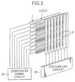
organic EL device 20, in which theemission layer 3 is omitted, and the emission substance is contained in theelectron transfer layer 2 as described above, so that theemission 18 of a prescribed wavelength is formed at the boundary between theelectron transfer layer 2 and thehole transfer layer 4. - Fig. 3 shows a specific example of the above-described organic EL device. It is constituted in such a manner that a laminated body of the organic layers (the
hole transfer layer 4, theemission layer 3 and the electron transfer layer 2) is provided between thecathode 1 and theanode 5; these electrodes are formed in the form of stripes that cross each other to form a matrix; a signal voltage is applied in time sequence by abrightness signal circuit 34 and acontroller circuit 35 having a shift register, to form emission at each of the numerous points of intersection (pixels). - Therefore, by using such a constitution, it can be used as an image reproducing apparatus, in addition to a display. It can be constituted as for a full color or multi-color display by arranging the pattern of the stripes for each of the colors, R, G and B.
- In the display device comprising plural pixels using such an organic EL device, the organic
thin film layers transparent electrode 5 and themetallic electrode 1, and emit light to the side of thetransparent electrode 5. - However, the organic EL device still has problems unsolved.
- Stable emission of the three primary colors, R, G and B is the necessary condition of the application of the organic EL device to a color display. When different series of material are used in these three systems of R, G and B in the process for producing the device, the production steps become extremely complicated and a long period of time is required.
- An object of the invention is to provide an electroluminescence device that can be easily produced with a low cost and has a device structure capable of conducting stable emission, and a process for producing the same.
- The inventors have conducted earnest investigations for the above-described circumstances, and have found that the device can be easily produced with a low cost by using the common material as possible in at least three kinds of laminated bodies having emission regions for the respective colors, so as to attain the invention.
- Accordingly, a first aspect of the invention relates to an electroluminescence device comprising at least three kinds of laminated bodies, in each of which an emission region is independently present in each of a hole transfer layer and an electron transfer layer, the laminated bodies comprising the hole transfer layers each comprising a layer comprising a common material, and the electron transfer layers each comprising a layer comprising a common material, and the electroluminescence device emitting at least three colors of light.
- A second aspect of the invention relates to an electroluminescence device comprising two kinds of laminated bodies, in each of which an emission region is independently present in each of a hole transfer layer and an electron transfer layer, the laminated bodies comprising the hole transfer layers each comprising a layer comprising a common material, and the electron transfer layers each comprising a layer comprising a common material, and the electroluminescence device emitting two colors of light.
- According to the electroluminescence device of the invention, because the hole transfer layers and the electron transfer layers each comprise the common material layer within each of the laminated bodies, in which the emission region is independently present in each of the hole transfer layer and the electron transfer layer, the laminated bodies for each of the colors of emission light can be easily produced with a low cost. By forming the common layers on the whole surface of an effective pixel region by using a mask with a large opening, the film formation property and the step coverage property become good, and a leakage current between the cathode and the anode can be reduced.
- The invention also provides a process for producing an electroluminescence device, as a process for producing the electroluminescence device of the first aspect of the invention with good reproducibility, which comprises
- a step of forming a first electrode, which is common in at least three kinds of the laminated bodies, on a common substrate,
- a step of forming the hole transfer layers by film formation of a common hole transfer layer forming material on a region containing at least three kinds of the laminated bodies on the first electrode,
- a step of forming the electron transfer layers by film formation of a common electron transfer layer forming material on a region containing at least three kinds of the laminated bodies on a region containing the hole transfer layers, and
- a step of forming second electrodes for at least three kinds of the laminated bodies on the electron transfer layers, to face the first electrode.
-
- The invention also provides a process for producing an electroluminescence device, as a process for producing the electroluminescence device of the second aspect of the invention with good reproducibility, which comprises
- a step of forming a first electrode, which is common in two kinds of the laminated bodies, on a common substrate,
- a step of forming the hole transfer layers by film formation of a common hole transfer layer forming material on a region containing two kinds of the laminated bodies on the first electrode,
- a step of forming the electron transfer layers by film formation of a common electron transfer layer forming material on a region containing two kinds of the laminated bodies on a region containing the hole transfer layers, and
- a step of forming second electrodes for two kinds of the laminated bodies on the electron transfer layers, to face the first electrode.
-
-
- Fig. 1 is a schematic cross sectional view showing an example of the conventional organic EL device;
- Fig. 2 is a schematic cross sectional view showing another example of the conventional organic EL device;
- Fig. 3 is a schematic perspective view showing a specific example of the conventional organic EL device;
- Figs. 4A to 4C are schematic cross sectional views of the organic EL device in a first embodiment according to the first aspect of the invention, in which Fig. 4A is the blue emission element; Fig. 4B is the green emission element; and Fig. 4C is the red emission element;
- Fig. 5 is a band model diagram schematically showing the laminated structure of the organic EL device according to the embodiment as shown in Fig. 4A;
- Fig. 6 is a graph showing the spectroscopic characteristics of the organic EL device according to Example 1 of the invention;
- Fig. 7 is a schematic cross sectional view of the vapor deposition apparatus used in the embodiment as shown in Fig. 5;
- Fig. 8 is a schematic plan view of the vapor deposition masks used in the embodiment as shown in Fig. 5, and the organic EL device produced;
- Fig. 9A is a cross sectional view perpendicular to the anode of an important part of the organic EL device according to the invention; and Fig. 9B is a cross sectional view along the anode taken along (B)-(B) line of Fig. 9A;
- Fig. 10 is a schematic disintegrated perspective view of the organic EL device as shown in Figs. 9A and 9B;
- Fig. 11 is a schematic cross sectional view of an important part of the organic EL device in a second embodiment according to the first aspect of the invention;
- Fig. 12 is a schematic cross sectional view of an important part of the organic EL device in a third embodiment according to the first aspect of the invention;
- Figs. 13A and 13B are schematic cross sectional views of the organic EL device in a fourth embodiment according to the second aspect of the invention, in which Fig. 13A is the blue emission element; and Fig. 13B is the green emission element;
- Fig. 14 is a schematic plan view of the vapor deposition masks used in the embodiment as shown in Figs. 13A and 13B, and the organic EL device produced;
- Fig. 15 is a cross sectional view of an important part of the organic EL device according to an example of the invention;
- Figs. 16A and 16B are schematic plan views of an important part of the organic EL device as shown in Fig. 15;
- Fig. 17A is a cross sectional view perpendicular to the anode of an important part of the organic EL device according to another example of the invention; and Fig. 17B is a cross sectional view along the anode taken along (B)-(B) line of Fig. 17A;
- Fig. 18 is a schematic disintegrated perspective view of the organic EL device as shown in Figs. 17A and 17B;
- Fig. 19 is a schematic cross sectional view of an important part of the organic EL device in a fifth embodiment according to the second aspect of the invention;
- Fig. 20 is a schematic cross sectional view of an important part of the organic EL device in a sixth embodiment according to the second aspect of the invention;
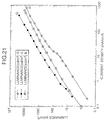
- Fig. 21 is a graph showing the current-luminance characteristics of the organic EL device according to Example 1;
- Fig. 22 is a graph showing the spectroscopic characteristics of the organic EL device according to Example 3;
- Fig. 23 is a graph showing the current-luminance characteristics of the organic EL device according to Example 3;
- Fig. 24 is a graph showing the current-luminance characteristics of the organic EL device according to Example 3;
- Fig. 25 is a graph showing the spectroscopic characteristics of the organic EL device according to Example 4;
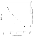
- Fig. 26 is a graph showing the current-luminance characteristics of the organic EL device according to Example 4;
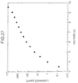
- Fig. 27 is a graph showing the current-luminance characteristics of the organic EL device according to Example 4;
- Fig. 28 is a graph showing the spectroscopic characteristics of the organic EL device according to Example 5; and
- Fig. 29 is a graph showing the current-luminance characteristics of the organic EL device according to Example 5.
-
- In the electroluminescence device and its production process of the first aspect of the invention, it is preferred that the emission region comprises an organic compound, it comprises at least three kinds of the laminated bodies each comprising an organic substance containing the emission region, in at least one of the laminated bodies, blue emission is obtained by recombination of an electron and a hole in a hole transfer organic material.
- According to such an electroluminescence device, emission can be obtained by the recombination of an electron and a hole in the hole transfer organic material (that is, the hole transfer layer has a structure also serving as an emission layer, i.e., the recombination region of an electron and a hole), and thus stable and high luminance emission, particularly blue emission, becomes possible with low voltage driving.
- Therefore, in the electroluminescence device that has a structure difficult to be realized due to the absence of a non-emission excellent electron transfer material (particularly, a thin amorphous organic electroluminescence device of low voltage driven and self-emission), the hole transfer layer also serves as an emission layer, and a long-life electroluminescence device having a device structure that can provide stable emission for a long period of time.
- Accordingly, in the organic electroluminescence device having a hole transfer layer serves as an emission layer, stable emission with high luminance and high efficiency can be obtained. This is conspicuous in blue emission, and a luminance of 10,000 cd/m2 or more can be obtained by DC driven, or a peak luminance of 55,000 cd/m2 in terms of direct current conversion can be obtained by pulse driven at a duty factor of 1/100.
- In addition to the blue emission device, green emission, as well as red emission and yellow emission by further doping are possible, and adjustment of chromaticity can be conducted by doping. Accordingly, an organic electroluminescence blue emission device that can emit blue light of excellent chromaticity with high luminance can be produced, and possibility and reduction in time on development of materials, and design concept in novel emission materials and electron transfer materials can be indicated.
- In the electroluminescence device and its production process of the first aspect of the invention, the emission region is mainly the organic hole transfer layer, and it preferably has a hole block layer for causing the recombination in the hole transfer layer.
- The hole block layer is preferably provided between the hole transfer layer and the electron transfer layer.
- It is preferred that the highest occupied molecular orbital level of the hole block layer is lower than the lower one in energy of the highest occupied molecular orbital levels of the organic layers (particularly, the hole transfer layer and the electron transfer layer) laminated in contact with both sides of the hole block layer.
- It is also preferred that the lowest unoccupied molecular orbital level of the hole block layer is higher than the lower one in energy of the lowest unoccupied molecular orbital levels of the organic layers (particularly, the hole transfer layer and the electron transfer layer) laminated in contact with both sides of the hole block layer, and is lower than the higher one in energy of them.
- The hole block layer preferably comprises a non-emission material of a low fluorescence yield, and may have a laminated structure comprising plural layers.
- Furthermore, while the hole block layer is not limited in material, it preferably comprises a non-emission material of a low fluorescence yield to prevent the formation of an exciplex (dimer) at the boundary to the hole transfer emission layer (i.e., reduction in emission efficiency)
- The emission region preferably comprises a hole transfer material for emission of short wavelength light. As the material that can be used in the hole block layer, a phenanthroline derivative of the following formula (1) is preferred:(wherein R1 to R8 each represents a hydrogen atom, a substituted or unsubstituted alkyl group, a substituted or unsubstituted aryl group, a substitued or unsubstitued amino group, a halogen atom, a nitro group, a cyano group or a hydroxyl group). Specific examples includes, for example, materials of the structural formulas (2) to (11).


- Furthermore, it is preferred that the emission region comprises an organic compound, it comprises at least three kinds of the laminated bodies each comprising an organic substance containing the emission region, and in at least one of the laminated bodies, green emission is obtained by recombination of an electron and a hole in an electron transfer organic material.
- It is also preferred that the emission region comprises an organic compound, it comprises at least three kinds of the laminated bodies each comprising an organic substance containing the emission region, and in at least one of the laminated bodies, red emission is obtained by recombination of an electron and a hole in an electron transfer organic material.
- By laminating the organic layer for obtaining blue emission by the recombination of an electron and a hole in the emission region as the hole block layer, an organic electroluminescence device having a hole transfer emission layer that can stably exhibit high luminance with low voltage driven can be obtained, and at the same time, an excellent organic electroluminescence device that can serve at least R, G and B can be provided, in which red or green emission by the recombination of an electron and a hole in the electron transfer layer can be obtained in the laminated region of the organic material in the absence of the hole block layer.
- In the second aspect of the invention, by laminating the organic layer for obtaining blue emission by the recombination of an electron and a hole in the emission region as the hole block layer, an organic electroluminescence device having a hole transfer emission layer that can stably exhibit high luminance with low voltage driven can be obtained, and at the same time, an excellent organic electroluminescence device that can serve G and B can be provided, in which green emission by the recombination of an electron and a hole in the electron transfer layer can be obtained in the laminated region of the organic material in the absence of the hole block layer.
- In the above-described device, it is preferred that a transparent electrode, an organic layer (particularly, the organic hole transfer layer, the hole block layer and the organic electron transfer layer), and a metallic electrode are laminated in this order on an optically transparent substrate.
- In this case, it is preferred that the device comprises an organic electroluminescence device, in which the transparent electrode, the organic layer and the metallic electrode form a matrix pattern on the same substrate.
- Accordingly, the above-described device becomes a preferred organic electroluminescence emission device and becomes suitable for a device for a color display.
- Preferred embodiments of the invention are explained below.
- Figs. 4A to 4C are schematic cross sectional views showing an important part of an
organic EL device 21 in a first embodiment according to the first aspect of the invention. - The
organic EL device 21 of this embodiment comprises anorganic electroluminescence elements 21B (blue), 21G (green) and 21R (red) each comprising a laminated body of amorphous organic thin films for emission of at least three kinds of light on acommon glass substrate 6. - In the
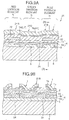
blue emission element 21B shown in Fig. 4A, atransparent electrode 5 comprising an indium oxide, etc. (hereinafter the same) doped with ITO (indium tin oxide) or Zn is formed on theglass substrate 6 as a row or line electrode by a method such as sputtering or vacuum evaporation, and a holetransfer emission layer 4a for blue emission, a holetransfer emission layer 4b, ahole block layer 33, an electron transfer layer (or an electron transfer emission layer) 2, and acathode 1 as a column electrode are laminated thereon in this order by a vacuum evaporation method. - In the
green emission element 21G shown in Fig. 4B, thetransparent electrode 5 comprising ITO, etc. is formed on theglass substrate 6 by a method such as sputtering or vacuum evaporation, and the holetransfer emission layers electron transfer layer 2 for green emission, and thecathode 1 as a column electrode are laminated thereon in this order by a vacuum evaporation method, with the hole block layer being not provided. - In the
red emission element 21R shown in Fig. 4C, thetransparent electrode 5 comprising ITO, etc. is formed on theglass substrate 6 by a method such as sputtering or vacuum evaporation, and the holetransfer emission layers electron transfer layer 32 for red emission, theelectron transfer layer 2, and thecathode 1 as a column electrode are laminated thereon in this order by a vacuum evaporation method. - The characteristic feature of the
organic EL device 21 of Figs. 4A to 4C resides in that thetransparent electrode 5 is formed as a row electrode or a line electrode, which is common in at least three kinds of theemission elements glass substrate 6, which is common in the emission elements; on the transparent electrode, the hole transfer layers 4a and 4b formed from the hole transfer layer forming material, which are common to each other, are formed on a region containing the emission elements, are formed; the electron transfer layers 2 formed from the electron transfer layer forming material, which is common to each other, is formed on a region containing the emission elements, are formed on the region containing the hole transfer layers; and on the electron transfer layers, thecathodes 1 are formed for the respective emission elements in the form of a matrix pattern facing thetransparent electrode 5. The emission elements each have a unique layer constitution, and theblue emission element 21B and thered emission element 21R have thehole block layer 33 and thered emission layer 32, respectively, in the form of a stripe pattern. - Therefore, in each of the emission elements, because the emission region comprises the hole transfer layers 4 (4a and 4b) and the
electron transfer layers 2 comprising the common material, a laminated body (matrix) in the form of stripes exhibiting emission of each colors of light can be easily produced with a low cost. Furthermore, on the whole surface of an effective pixel region, by forming the common layers by using a mask with a large opening, the film formation property and the step coverage property become well, and a leakage current between the cathode and the anode can be reduced. - The
blue emission element 21B is constituted as a structure having thehole transfer layer 4 that also serves as an emission layer, and its basic structure is the same as in other embodiments described later. - The characteristic feature of the
element 21B in this embodiment resides in that because thehole block layer 33 is laminated as being inserted between thehole transfer layer 4 and theelectron transfer layer 2, the recombination of an electron and a hole in thehole transfer layer 4 is accelerated, and emission in thehole transfer layer 4 is obtained. - Fig. 5 is a schematic view showing the laminated structure of this embodiment (Fig. 4A) described above as a band model.
- In Fig. 5, the thick lines (L1 and L2) shown in the layers of the
cathode 1 comprising Al and Al-Li (aluminum-lithium) and the ITOtransparent electrode 5 are approximate work functions of the metals of them; and in the layers between the both electrodes, the thick lines on the upper side l1, l2, l3 and l4 and the numerals show the levels of the lowest unoccupied molecular orbital (LUMO) of them, and the thick lines on the lower side l5, l6, l7 and l8 and the numerals show the levels of the highest occupied molecular orbital (HOMO) of them. The energy level values in Fig. 5 are only an example and vary depending on the materials. - In this organic EL device, as shown in Fig. 5, a hole h injected from the
transparent electrode 5 as an anode migrates through thehole transfer layer 4, and an electron e injected from themetallic electrode 1 as a cathode migrates through theelectron transfer layer 2, and as a result, the electron-hole recombination occurs in thehole transfer layer 4 to form emission. - Since the electron e injected from the
metallic electrode 1 as a cathode has a nature of migrating toward the direction of lower energy level, it can reach the holetransfer emission layers metallic electrode 1, theelectron transfer layer 2, thehole block layer 33, the holetransfer emission layer 4b and the holetransfer emission layer 4a in this order. - On the other hand, since the hole h injected from the ITO
transparent electrode 5 as an anode has a nature of migrating toward the direction of higher energy level, it can migrate to theelectron transfer layer 2 through the highest occupied molecular orbital (HOMO) levels l5, l6, and l7 of the holetransfer emission layers hole block layer 33 in this order. - As shown in Fig. 5, however, because the highest occupied molecular orbital (HOMO) level l8 of the
electron transfer layer 2 is lower than the highest occupied molecular orbital (HOMO) level l7 of thehole block layer 33, the hole h thus injected is difficult to migrate from thehole block layer 33 to theelectron transfer layer 2, and is filled in thehole block layer 33. - As a result, the hole h filled in the
hole block layer 33 accelerates the electron-hole recombination in thehole transfer layer 4, and emission is conducted by the emission materials of the holetransfer emission layers hole transfer layer 4. - Accordingly, by providing the
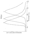
hole block layer 33, the transfer of the hole h is effectively controlled by thehole block layer 33 to effectively occur the electron-hole recombination in thehole transfer layer 4. Among the holetransfer emission layers transfer emission layer 4b adjacent to thehole block layer 33 is assisted by the emission of the holetransfer emission layer 4a, and light having a certain wavelength (blue color) is emitted as shown in Fig. 6. - The electron-hole recombination inherently occurs in each of the
electron transfer layer 2 and thehole transfer layer 4 by the injection of an electron from thecathode 1 and the injection of a hole from theanode 5. Therefore, in the case where thehole block layer 33 described above is not present, the recombination of an electron and a hole occurs at the boundary of theelectron transfer layer 2 and thehole transfer layer 4, and only light of a long wavelength can be obtained. However, by providing thehole block layer 33 as described above, blue emission can be accelerated with thehole transfer layer 4 containing an emission substance as the emission region. - The
hole block layer 33 is to control the transfer of a hole h as described above. In order to realize such control, it is only required that the highest occupied molecular orbital (HOMO) of thehole block layer 33 is lower than the lower level of the highest occupied molecular orbital (HOMO) in energy of the highest occupied molecular orbital (HOMO) levels of the holetransfer emission layer 4b and theelectron transfer layer 2; and the lowest unoccupied molecular orbital (LUMO) of thehole block layer 33 is higher than the lower one of the lowest unoccupied molecular orbital (LUMO) in energy of the lowest unoccupied molecular orbital (LUMO) levels of the holetransfer emission layer 4b and theelectron transfer layer 2, and is lower than the higher level of the lowest unoccupied molecular orbital (LUMO) in energy of them, and thus it is not limited to the above-described constitution. - The
hole block layer 33 may be formed from various materials, and its thickness may vary within the range where its function can be maintained. While the thickness is preferably from 1 Å to 1,000 Å (from 0.1 nm to 100 nm), if it is too thin, the function of hole blocking tends to be incomplete, and the recombination region is liable to bridge the hole transfer layer and the electron transfer layer, and if it is too thick, emission may not be conducted due to increase in a film resistance. - In the
green emission element 21G, since thehole block layer 33 is not provided, a hole migrates into theelectron transfer layer 2 to cause the electron-hole recombination in theelectron transfer layer 2, and emission is conducted by theelectron transfer layer 2 to emit light having a certain wavelength (green color) as shown in Fig. 6. - In the
red emission element 21R, since thered emission layer 32 is provided instead of thehole block layer 33, a hole migrates into theemission layer 32 to cause the electron-hole recombination in theemission layer 32, and emission is conducted by theemission layer 32 to emit light having a certain wavelength (red color) as shown in Fig. 6. - The
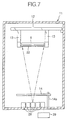
organic EL device 21 is produced by using avapor deposition apparatus 11 shown in Fig. 7. The apparatus has in its inside a pair of holding means 13 fixed under anarm 12, and a stage structure (omitted from the figure) capable of setting atransparent glass substrate 6 facing downward and amask 22 is provided between a pair of the fixing means 13. Ashutter 14 supported by a bearingshaft 14a is provided under theglass substrate 6 and themask 22, variousvapor deposition sources 28 are provided thereunder. The vapor deposition sources are heated by a resistance heating method by apower source 29. The heating is also conducted by an EB (electron beam) heating method depending on necessity. - In the apparatus described above, the
mask 22 is for the pixels, and theshutter 14 is for the vapor deposition materials. Theshutter 14 rotates with the bearingshaft 14a as the center, and cuts off a vapor stream of the vapor deposition material depending on the sublimation temperature of the material. - As the
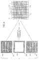
mask 22, three kinds of them shown in Fig. 8 are actually used, and various types of formation are conducted to form a prescribed pattern with suitably interchanging them. Thehole transfer layer 4 is formed by using amask 22a through alarge opening 23a as common to the elements; thehole block layer 33 is formed by using amask 22b through aopening 23b in the form of slits to have a prescribed pattern for theblue emission element 21B; thered emission layer 32 is formed by using amask 22c through anopening 23c in the form of slits to have a prescribed pattern for thered emission element 21R; theelectron transfer layer 2 is formed by using themask 22a through thelarge opening 23a as common to the elements; and thecathode 1 is formed by using a mask (not shown in the figure) to have a prescribed pattern for the elements. - As a result, the
emission elements transparent electrode 5 on thecommon glass substrate 6, as shown in Fig. 8. These stripes are divided into each of the emission regions by an insulating layer (not shown in the figure). By forming the emission elements on thetransparent electrode 5 to have the same pattern, the carrier transfer property between the cathode and the anode is improved, and voltage drop between the electrodes can be reduced. - Figs. 9A, 9B and 10 show a specific example of the
organic EL device 21 produced by the vapor deposition apparatus described above. After vapor depositing an ITO transparent electrode to be a line electrode on aglass substrate 6,SiO 2 24 is vapor deposited by the vacuum deposition method in the column direction to have a prescribed pattern to expose thetransparent electrode 5 between the SiO2 in the form of the pixel pattern. Then,organic layers metallic electrode 1 as a column electrode (for example, a laminated body of anLiF layer 1a and anAl layer 1b) are formed in this order by using vapor deposition masks in the column direction to have the stripe pattern, so as to produce a matrix. Thevapor deposition masks organic layers organic layers transparent electrode 5 in the line direction, they may be formed in the column direction perpendicular to thetransparent electrode 5. - According to the
organic EL device 21, in each of the emission elements, because the emission regions are independently present in each of the hole transfer layer 4 (4a and 4b) and the electron transfer layer 2 (32), and the hole transfer layer 4 (4a and 4b) and theelectron transfer layer 2 are formed from the common materials, respectively, in each of the emission elements, a laminated body in the form of stripes (matrix) exhibiting emission light of each of the colors can be produced by a simple process with a low cost. Furthermore, because it has theorganic layers layer 24, and stable performance with high reliability with a small leakage current between the cathode and the anode can be obtained. This effect can be further improved by making the shape of the upper surface of the insulatinglayer 24 to have curved surface, as shown by the broken line in Fig. 9B. - In the
vapor deposition apparatus 11 described above, a shape and a size of the pixels can be changed other than one having the pixels shown in Figs. 9A, 9B and 10, and a number of small pixels can be individually formed, whereas a large pixel can be singly formed. - The transparent electrode, the organic hole transfer layer, the organic hole block layer, the red emission layer, the organic electron transfer layer and the metallic electrode of the electroluminescence device described above each may have a laminated structure comprising plural layers.
- The organic layers of the electroluminescence device may be formed by other film formation methods utilizing sublimation or evaporation, or methods such as spin coating or casting.
- The hole transfer emission layer of the electroluminescence device may be formed with co-evaporation of a slight amount of molecules for controlling the emission spectrum of the device. For example, it may be an organic thin film containing a slight amount of an organic substance, such as a perylene derivative and a coumarin derivative.
- While the electroluminescence device is suitable for emission of three colors R, G and B, other emission colors can be obtained depending on the species of the emission materials used.
- Examples of the material that can be used as the hole transfer material include benzidine and its derivatives, styrylamine and its derivatives, and triphenylmethane and its derivatives, as well as porphyrin and its derivatives, triazole and its derivatives, imidazole and its derivatives, oxadiazole and its derivatives, polyarylalkane and its derivatives, phenylenediamine and its derivatives, arylamine and its derivatives, oxazole and its derivatives, anthracene and its derivatives, fluorenone and its derivatives, hydrozone and its derivatives, and stilbene and its derivatives, or a monomer, an oligomer or a polymer of a heterocyclic conjugated system such as a polysilane series compound, a vinylcarbazole series compound, a thiophene series compound, and an aniline series compound.
- Specifically, α-naphthylphenyldiamine, porphyrin, metallic tetraphenylporphyrin, metallic naphthalocyanine, 4,4'4''-trimethyltriphenylamine, 4,4',4''-tris(3-methylphenylphenylamino)triphenylamine, N,N,N',N'-tetrakis(p-tolyl)p-phenylenediamine, N,N,N',N'-tetraphenyl-4,4'-diaminebiphenyl, N-phenylcarbazole, 4-di-p-tolylaminostilbene, poly(paraphenylenevinylene), poly(thiophenevinylene), poly(2,2'-thenylpyrrol), etc. can be exemplified, but it is not limited to them.
- Examples of the materials that can be used as the electron transfer material include quinoline and its derivatives, perylene and its derivatives, bis-styryl and its derivatives, pyrazine and its derivatives, etc.
- Specifically, 8-hydroxyquinoline aluminum, anthracene, naphthalene, phenanthrene, pyrene, chrysene, perylene, butadiene, coumarin, acridine, stilbene, and their derivatives, etc. can be exemplified.
- Examples of the materials for red emission include BSB-BCN, as well as the above-described electron transfer materials doped with DCM, DCM2, Nile Red, phenoxazine, etc.
- The anode and the cathode of the electroluminescence device described above are not limited in materials used.
- For the cathode material, a metal having a work function of a small difference from the vacuum level of the electrode material is preferably used to effectively inject an electron. In addition to an aluminum-lithium alloy, a metal having a low work function, such as aluminum, indium, magnesium, silver, calcium, barium and lithium, may be used singly, or as an alloy with other metal to improve the stability.
- While ITO as a transparent electrode is used as the anode in the example described later for withdrawing organic electroluminescence light from the side of the anode, in order to effectively inject a hole, one having a work function with a large difference from the vacuum level of the anode material, such as gold, a mixture of tin dioxide and antimony and a mixture of zinc oxide and aluminum, may be used.
- An organic electroluminescence device for full color or multi-color emitting three colors R, G and B can be produced by selecting the emission materials. The invention can be applied not only for a display, but also for an organic electroluminescence device for a light source, as well as other optical uses.
- The organic electroluminescence device may be sealed with germanium oxide, etc. to avoid influence of oxygen in the air to improve the stability, and the device is operated under withdrawing to vacuum.
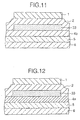
- Fig. 11 is a schematic cross sectional view showing an important part of a
blue emission element 21B in a second embodiment according to the first aspect of the invention. - In the organic EL device according to this embodiment, there is differences from the device of Figs. 4A to 4C in that a hole
transfer emission layer 4b is formed on an ITOtransparent electrode 5, and the hole transfer emission layer is formed in the form of a single layer. Thegreen emission element 21G and thered emission element 21R other than this are the same as the device of Figs. 4A to 4C. - Fig. 12 is a schematic cross sectional view showing an important part of a
blue emission element 21B in a third embodiment according to the first aspect of the invention. - In the organic EL device according to this embodiment, there is differences from the device of Figs. 4A to 4C in that a hole transfer layer (also serving as a hole transfer emission layer) 4a is formed on an ITO
transparent electrode 5, and the hole transfer emission layer is formed in the form of a single layer, as similar to the second embodiment described above. The other parts than this are the same as the second embodiment. - Figs. 13A and 13B are schematic cross sectional views showing an important part of an
organic EL device 21 in a fourth embodiment according to the second aspect of the invention. - The
organic EL device 21 of this embodiment comprises anorganic electroluminescence elements 21B (blue) and 21G (green) each comprising a laminated body of amorphous organic thin films for emission of two kinds of light on acommon glass substrate 6. - In the
blue emission element 21B shown in Fig. 13A, atransparent electrode 5 comprising an indium oxide, etc. (hereinafter the same) doped with ITO or Zn is formed on theglass substrate 6 as a row or line electrode by a method such as sputtering or vacuum evaporation, and a holetransfer emission layer 4a for blue emission, a holetransfer emission layer 4b, ahole block layer 33, an electron transfer layer (or an electron transfer emission layer) 2, and acathode 1 as a column electrode are laminated thereon in this order by a vacuum evaporation method. - In the
green emission element 21G shown in Fig. 13B, thetransparent electrode 5 comprising ITO, etc. is formed on theglass substrate 6 by a method such as sputtering or vacuum evaporation, and the holetransfer emission layers electron transfer layer 2 for green emission, and thecathode 1 as a column electrode are laminated thereon in this order by a vacuum evaporation method, with the hole block layer being not provided. - The characteristic feature of the
organic EL device 21 of Figs. 17A and 17B resides in that thetransparent electrode 5 is formed as a row electrode or a line electrode, which is common in two kinds of theemission elements glass substrate 6, which is common in the emission elements; on the transparent electrode, the holetransfer emission layers electron transfer layers 2 are formed from the electron transfer layer forming material, which is common in the emission elements, on the region containing the hole transfer layers; and on the electron transfer layers, thecathodes 1 are formed for the respective emission elements to face the transparent electrode 5 (or in the form of a matrix pattern). The emission elements each have a unique layer constitution, and theblue emission element 21B has thehole block layer 33, for example, in the form of a stripe pattern, but thehole block layer 33 is not provided for thegreen emission element 21G. - Therefore, in each of the emission elements, because the emission regions are independently present in the hole transfer layers 4 (4a and 4b) and the
electron transfer layers 2, and the hole transfer layers 4 (4a and 4b) and theelectron transfer layers 2 each comprises the common materials for the emission regions, the laminated body exhibiting emission of each colors of light can be easily produced with a low cost. Furthermore, on the whole surface of an effective pixel region, by forming the common layers by using a mask with a large opening, the film formation property and the step coverage property become well, and a leakage current between the cathode and the anode can be reduced. Because it can exhibit two-color display, it is suitable for display of characters. - As a result, the
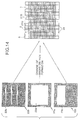
emission elements transparent electrode 5 on thecommon glass substrate 6, as shown in Fig. 14. These may be in the form of stripes, and the stripes may be divided into each of the emission regions by an insulating layer (not shown in the figure). In this case, by forming the emission elements on thetransparent electrode 5 to have the same pattern, the carrier transfer property between the cathode and the anode is improved, and voltage drop between the electrodes can be reduced. While theorganic layer 33 is formed in the line direction on thetransparent substrate 5, it may be formed in the column direction perpendicular to thetransparent substrate 5. - Figs. 15, 16A, 16B, 17A, 17B and 18 show two kinds of specific examples of the
organic EL devices 21 and 21' produced by the vapor deposition apparatus described above. In the example shown in Figs. 15, 16A and 16B, an ITOtransparent electrode 5 is vapor deposited on aglass substrate 6 by using the vapor deposition apparatus described above, and ablue emission element 21B and agreen emission element 21G are formed as connecting to each other in the region surrounded by an insulatinglayer 24 such as SiO2, where thetransparent electrode 5 is exposed in the form of the pixel pattern inside the insulating layer. Then,organic layers LiF layer 1a and anAl layer 1b) are commonly formed on the emission elements. This example is suitable for displaying characters as shown in Fig. 16B utilizing the emission pattern schematically shown in Fig. 16A. In the example shown in Figs. 17A, 17B and 18, after vapor depositing an ITOtransparent electrode 5 to be a line electrode,SiO 2 24 is vapor deposited in the column direction to have a prescribed pattern to expose thetransparent electrode 5 between the SiO2 in the form of the pixel pattern. Then,organic layers electrode 1 is formed as a column electrode in the form of a stripe pattern in the column direction, so as to produce a matrix. Thevapor deposition masks organic layers - Fig. 19 is a schematic cross sectional view showing an important part of a
blue emission element 21B in a fifth embodiment according to the second aspect of the invention. - In the organic EL device according to this embodiment, there is differences from the device of Figs. 17A and 17B in that a hole
transfer emission layer 4b is formed on an ITOtransparent electrode 5, and the hole transfer emission layer is formed in the form of a single layer. Thegreen emission element 21G other than this is the same as the device of Figs. 17A and 17B. - Fig. 20 is a schematic cross sectional view showing an important part of a
blue emission element 21B in a sixth embodiment according to the second aspect of the invention. - In the organic EL device according to this embodiment, there is differences from the device of Figs. 17A and 17B in that a hole transfer layer (also serving as a hole transfer emission layer) 4a is formed on an ITO
transparent electrode 5, and the hole transfer emission layer is formed in the form of a single layer, as similar to the second embodiment described above. The other parts than this are the same as the second embodiment. - The invention is described in more detail with reference to the examples below.
- The specific constitution of the
organic EL device 21 of this example is explained based on its production process. - In order to produce a simple matrix of 12 combinations of R, G and B stripes having a dimension of 30 mm x 36 mm, 36 of
ITO electrodes 5, for example, having a thickness of about 100 nm with a width of 1.15 mm and a distance of 0.1 mm, were formed on aglass substrate 6 having a dimension of 53 mm x 53 mm, and 31 of insulatinglayers 24 with a width of 0.5 mm and a distance of 1.0 mm were formed by vapor deposition of SiO2 on the column side. Therefore, the emission region of one cell for producing the organic electroluminescence device was 1.0 mm x 1.15 mm, and the opening ratio was 60.8%. - On the ITO
transparent electrode 5, m-MTDATA (4,4'4''-tris(3-methylphenylphenylamino)triphenylamine having the formula (12)) was vapor deposited as a holetransfer emission layer 4a by a vacuum vapor deposition method under vacuum to a thickness of 30 nm at a vapor deposition rate of from 0.2 to 0.4 nm/sec on the whole surface including theITO electrode 5 by using amask 22a having anopening 23a having an area of 40.0 mm x 48.0 mm.
- On the hole
transfer emission layer 4a, α-NPD (α-naphtylphenyldiamine having the formula (13), which could be α-PPD of the formula (14), α-TPD of the formula (15) or TPD of the formula (16)) was vapor deposited as a holetransfer emission layer 4b at a thickness of 50 nm (vapor deposition rate: from 0.2 to 0.4 nm/sec), so as to form ahole transfer layer 4 having a two-layer structure having an emission function.

- On the
hole transfer layer 4, a phenanthroline derivative, such as bathocuproine (2,9-dimethyl-4,7-diphenyl-1,10-phenanthroline having the formula (3)) was vapor deposited (vapor deposition rate: from 0.2 to 0.4 nm/sec) on thetransparent electrode 5 as ahole block layer 33 at a thickness of 20 nm in the stripe pattern of 1.15 mm x 48.0 mm, which was an emission region of theITO electrode 5, with changing to amask 22b having 12openings 23b having a stripe form having an area of 1.16 mm x 49 mm. - On the
hole transfer layer 4, BSB-BCN (having the formula (17)) was vapor deposited (vapor deposition rate: from 0.2 to 0.4 nm/sec) on thetransparent electrode 5 as an electron transfer redemission material layer 32 at a thickness of 20 nm in the stripe pattern of 1.15 mm x 48.0 mm, which was an emission region of theITO electrode 5, with changing to amask 22c having 12openings 23c having a stripe form having an area of 1.16 mm x 49 mm.
- After changing to the
mask 22a having themask opening 23a having an area of 40.0 mm x 48.0 mm, Alq3 (8-hydorxy quinoline aluminum having the formula (18)) was vapor deposited at a thickness of 40 nm as an electron transfer layer or an electrontransfer emission layer 2.
- After changing to a mask having an opening having an area of 1.16 mm x 49 mm, Al-Li (an aluminum-lithium alloy: Li concentration: about 1 mol%) was vapor deposited at a thickness of about 0.5 nm as a
cathode 1, followed by further vapor depositing Al at a thickness of about 200 nm, to produce anorganic EL device 21 corresponding to R, G and B shown in Figs. 9A and 9B. - The device characteristics were measured for the organic EL device of this example, and the results are shown below.
- Fig. 6 is a graph showing the spectral characteristics of the
organic EL device 21 of Example 1 shown in Figs. 9A and 9B. The maximum emission wavelength in the emission region containing bathocuproine functioning as a hole block layer was 460 nm, and the coordinates on the CIE chromaticity coordinates were (0.155, 0.11), which resulted in good blue emission. It was apparent from the shape of the emission spectrum that it was emission from α-NPD. From the emission parts in the absence of bathocuproine, emission from Alq3 as the electron transfer emission material was obtained, from which good green emission having the maximum emission wavelength of 520 nm and CIE (0.33, 0.55) was obtained. From the parts in the form of stripes, on which BSB-BCN was vapor deposited between α-NPD and Alq3, good red emission having the maximum emission wavelength of 635 nm and CIE (0.60, 0.39) was obtained. - With respect to the luminance shown in Fig. 21, in the blue emission part, it was 10,000 cd/m2 at a current density of 500 mA/cm2, and the emission efficiency was 1.21 m/W at a current density of 1 mA/cm2. In the green emission part, it was 7,000 cd/m2 at a current density of 100 mA/cm2, and the emission efficiency was 1.11 m/W at a current density of 1 mA/cm2. In the red emission part, it was 5,600 cd/m2 at a current density of 500 mA/cm2, and the emission efficiency was 0.031 m/W at a current density of 1 mA/cm2.
- When the organic EL device was pulse driven at a duty factor of 1/100, the peak luminance converted to the direct current driven was 55,000 cd/m2 at a current density of 5,500 mA/cm2, and a high luminance blue emission element having high performance sufficient to practical use could be produced.
- The specific constitution of the
organic EL device 21 of this example is explained based on its production process. - In order to produce a simple matrix of 12 combinations of R, G and B stripes having a dimension of 30 mm x 36 mm, 36 of
ITO electrodes 5, for example, having a thickness of about 100 nm with a width of 1.15 mm and a distance of 0.1 mm, were formed on aglass substrate 6 having a dimension of 53 mm x 53 mm, and 31 of insulatinglayers 24 with a width of 0.5 mm and a distance of 1.0 mm were formed by vapor deposition of SiO2 on the column side. Therefore, the emission region of one cell for producing the organic electroluminescence device was 1.0 mm x 1.15 mm, and the opening ratio was 60.8%. - On the ITO
transparent electrode 5, m-MTDATA (4,4'4''-tris(3-methylphenylphenylamino)triphenylamine having the formula (12)) was vapor deposited as a holetransfer emission layer 4a by a vacuum vapor deposition method under vacuum to a thickness of 30 nm at a vapor deposition rate of from 0.2 to 0.4 nm/sec on the whole surface including theITO electrode 5 by using amask 22a having anopening 23a having an area of 40.0 mm x 48.0 mm. - On the hole
transfer emission layer 4a, α-NPD (α-naphtylphenyldiamine having the formula (13), which could be α-PPD of the formula (14), α-TPD of the formula (15) or TPD of the formula (16)) was vapor deposited as a holetransfer emission layer 4b at a thickness of 50 nm (vapor deposition rate: from 0.2 to 0.4 nm/sec), so as to form ahole transfer layer 4 having a two-layer structure having an emission function. - On the
hole transfer layer 4, a phenanthroline derivative, such as bathocuproine (2,9-dimethyl-4,7-diphenyl-1,10-phenanthroline having the formula (3)) was vapor deposited (vapor deposition rate: from 0.2 to 0.4 nm/sec) on thetransparent electrode 5 as ahole block layer 33 at a thickness of 20 nm in the stripe pattern of 1.15 mm x 48.0 mm, which was an emission region of theITO electrode 5, with changing to amask 22b having 12openings 23b having a stripe form having an area of 1.16 mm x 49 mm. - On the
hole transfer layer 4, DMC2 (having the formula (19)) and Alq3 (8-hydorxy quinoline aluminum having the formula (18)) was vapor deposited (vapor deposition rate: from 0.2 to 0.4 nm/sec) in such a manner that the molar ratio of DCM2 was from 0.5 to 1% on thetransparent electrode 5 as an electron transfer redemission material layer 32 at a thickness of 20 nm in the stripe pattern of 1.15 mm x 48.0 mm, which was an emission region of theITO electrode 5, with changing to amask 22c having 12openings 23c having a stripe form having an area of 1.16 mm x 49 mm.
- After changing to the
mask 22a having themask opening 23a having an area of 40.0 mm x 48.0 mm, Alq3 (8-hydorxy quinoline aluminum having the formula (18)) was vapor deposited at a thickness of 40 nm as an electron transfer layer or an electrontransfer emission layer 2. - After changing to a mask having an opening having an area of 1.16 mm x 49 mm, Al-Li (an aluminum-lithium alloy: Li concentration: about 1 mol%) was vapor deposited at a thickness of about 0.5 nm as a
cathode 1, followed by further vapor depositing Al at a thickness of about 200 nm, to produce anorganic EL device 21 corresponding to R, G and B shown in Figs. 9A and 9B. - The device characteristics were measured for the organic EL device of this example, and the results are shown below.
- As similar to the
organic EL device 21 according to Example 1, the maximum emission wavelength in the emission region containing bathocuproine functioning as a hole block layer was 460 nm, and the coordinates on the CIE chromaticity coordinates were (0.155, 0.11), which resulted in good blue emission. It was apparent from the shape of the emission spectrum that it was emission from α-NPD. From the emission parts in the absence of bathocuproine, emission from Alq3 as the electron transfer emission material was obtained, from which good green emission having the maximum emission wavelength of 520 nm and CIE (0.33, 0.55) was obtained. From the parts in the form of stripes, on which DCM2 and Alq3 was vapor co-deposited between α-NPD and Alq3, good red emission having the maximum emission wavelength of 645 nm and CIE (0.66, 0.34) was obtained. - With respect to the luminance, in the blue emission part, it was 10,000 cd/m2 at a current density of 500 mA/cm2, and the emission efficiency was 1.21 m/W at a current density of 1 mA/cm2. In the green emission part, it was 7,000 cd/m2 at a current density of 100 mA/cm2, and the emission efficiency was 1.11 m/W at a current density of 1 mA/cm2. In the red emission part, it was 160 cd/m2 at a current density of 250 mA/cm2, and the emission efficiency was 0.041 m/W at a current density of 1 mA/cm2.
- The organic EL device according to Example 3 of the invention is explained based on its production process.
- The organic EL device according to this example was the same as in Example 1, except that the hole
transfer emission layer 4a was not provided, and α-NPD (α-naphtylphenyldiamine having the formula (13), which could be α-PPD of the formula (14), α-TPD of the formula (15) or TPD of the formula (16)) was vapor deposited as a holetransfer emission layer 4b under vacuum to a thickness of 50 nm (vapor deposition rate: from 0.2 to 0.4 nm/sec), so as to form a hole transfer emission layer as a single layer. - Fig. 22 is a graph showing the spectral characteristics of the organic EL device according to Example 3 shown in Fig. 11.
- In this example, the maximum emission wavelength (absorption peak) was about 460 nm, and the coordinates on the CIE coordinates were (0.155, 0.11), and good blue emission was exhibited. The green emission and the red emission were the same as in Fig. 6.
- As shown in Fig. 23, the luminance was 1,400 cd/m2 at a current density of 400 mA/cm2.
- It was apparent from the shape of the emission spectrum that in the blue emission part, it was emission from the hole
transfer emission layer 4b comprising α-NPD. - Furthermore, as shown by the threshold value voltage characteristics of Fig. 24, the current did substantially not flow until a voltage of about 5 V, which gradually began to flow exceeding 5 V, and it suddenly flew exceeding 6 V. This means that it can be driven with a low voltage, and its threshold value voltage characteristics are good.
- The organic EL device according to Example 4 of the invention is explained based on its production process.
- In the organic EL device according to this example, m-MTDATA (4,4'4''-tris(3-methylphenylphenylamino)triphenylamine having the formula (12)) was vapor deposited as a hole
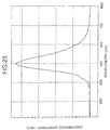
transfer emission layer 4a by a vacuum vapor deposition method under vacuum to a thickness of 50 nm (vapor deposition rate: from 0.2 to 0.4 nm/sec), and a hole transfer emission layer was formed as a single layer as similar to Example 3 described above. - Fig. 25 is a graph showing the spectral characteristics of the organic EL device according to Example 4 shown in Fig. 12.
- In this example, the maximum emission wavelength (absorption peak) was about 500 nm, and the coordinates on the CIE coordinates were (0.26, 0.47), and good green emission was exhibited. The red emission was the same as in Fig. 6.
- As shown in Fig. 26, the luminance was 280 cd/m2 at a current density of 110 mA/cm2 in the blue emission part.
- It was apparent from the shape of the emission spectrum that it was emission from the hole
transfer emission layer 4a comprising m-MTDATA. - From the voltage-luminance characteristics shown in Fig. 27, it can be driven with a low voltage, and the luminance was good.
- It is apparent from the above that in the organic EL devices of Examples 1 to 4 according to the invention, the hole transfer layer can serve as an emission layer due to sufficient electron-hole recombination in the hole transfer layer by providing the
hole block layer 33 between the holetransfer emission layer 4a and/or 4b and theelectron transfer layer 2, so as to obtain stable emission with high efficiency. - In addition to the blue emission in Examples 1 and 2, the green emission shown in Example 4, red emission by doping, and adjustment of chromaticity by doping were possible.
- According to the examples described above, an organic EL device providing blue emission of good chromaticity with high luminance can be produced even by using the conventional materials, and possibilities and reduction in time of material development are possible. Further, it is considered that design concept in novel emission materials and electron transfer materials can be indicated.
- The specific constitution of the organic EL device of this example is explained based on its production process.
- On an ITO substrate comprising a
glass substrate 6 of 30 mm x 30 mm having provided thereon an ITO electrode 5 (film thickness: about 100 nm),SiO 2 24 was vapor deposited to mask the other region than the emission region of 2 mm x 2 mm, to produce an ITO substrate for producing an organic electroluminescence device. - As a hole
transfer emission layer 4a, m-MTDATA (4,4',4''-tris (3-methylphenylphenylamino)triphenylamine having the formula (12)) was vaopr deposited by a vacuum vapor deposition method under vacuum to a thickness of 30 nm at a vapor deposition rate of from 0.2 to 0.4 nm/sec. - α-NPD (α-naphtylphenyldiamine having the formula (13)) functioning as a hole transfer layer or a hole
transfer emission layer 4b was vapor deposited by a vacuum vapor deposition method under vacuum to a thickness of 50 nm at a vapor deposition rate of from 0.2 to 0.4 nm/sec. - The mask was changed to a
mask 22c having anopening 23c having an area of 1 mm x 2 mm, which covered a half of the emission region of 2 mm x 2 mm, bathocuproine (2,9-dimethyl-4,7-diphenyl-1,10-phenanthroline having the formula (3)) was vapor deposited at a vapor deposition rate of from 0.2 to 0.4 nm/sec as ahole block layer 33 at a thickness of 20 nm. - The mask was changed to 22a having an
opening 23a of an area of 2 mm x 2 mm, Alq3 (8-hydorxy quinoline aluminum having the formula (18)) functioning as an electron transfer layer or an electrontransfer emission layer 2 was vapor deposited at a thickness of 40 nm. - As a
cathode 1, LiF was vapor deposited at a thickness of about 0.5 nm, followed by further vapor depositing Al at a thickness of about 200 nm, to produce anorganic electroluminescence device 21 emitting blue light and green light shown in Fig. 15. - The characteristics were measured for the organic electroluminescence device emitting blue light and green light, and the results are shown below.
- Fig. 28 is a graph showing the spectral characteristics of the
organic EL device 21 of Example 5. The maximum emission wavelength in the emission region containing bathocuproine functioning as a hole block layer was 460 nm, and the coordinates on the CIE chromaticity coordinates were (0.16, 0.14), which resulted in good blue emission. It was apparent from the shape of the emission spectrum that it was emission from α-NPD. From the emission parts in the absence of bathocuproine, emission from Alq3 as the electron transfer emission material was obtained, from which good green emission having the maximum emission wavelength of 520 nm and CIE (0.33, 0.55) was obtained. - With respect to the luminance shown in Fig. 29, at a current density of 350 mA/cm2, it was 6,000 cd/m2 in the blue emission part, and 40,000 cd/m2 in the green emission part.
- When the organic EL device was pulse driven at a duty factor of 1/100, the peak luminance converted to the direct current driven was 55,000 cd/m2 at a current density of 5,500 mA/cm2, and a high luminance blue emission element having high performance sufficient to practical use could be produced.
- The device emitting blue light and green light thus produced was a device having a blue emission region having an emission region of 1 mm x 2 mm, which was emission from α-NPD, and a green emission region having an emission region of 1 mm x 2 mm, which was emission from Alq3, in the same emission region having an emission region of 2 mm x 2 mm.
- The specific constitution of the organic EL device of this example is explained based on its production process.
- On an ITO substrate comprising a
glass substrate 6 of 30 mm x 30 mm having provided thereon an ITO electrode 5 (film thickness: about 100 nm),SiO 2 24 was vapor deposited to mask the other region than the emission region of 2 mm x 2 mm, to produce an ITO substrate for producing an organic electroluminescence device. - α-NPD (α-naphtylphenyldiamine having the formula (13)) functioning as a hole transfer layer or a hole
transfer emission layer 4b was vapor deposited by a vacuum vapor deposition method under vacuum to a thickness of 50 nm (vapor deposition rate: from 0.2 to 0.4 nm/sec). - The mask was changed to a
mask 22c having anopening 23c having an area of 1 mm x 2 mm, which covered a half of the emission region of 2 mm x 2 mm, bathocuproine (2,9-dimethyl-4,7-diphenyl-1,10-phenanthroline having the formula (3)) was vapor deposited as ahole block layer 33 at a thickness of 20 nm (vapor deposition rate: from 0.2 to 0.4 nm/sec). - The mask was changed to 22a having an
opening 23a of an area of 2 mm x 2 mm, Alq3 (8-hydorxy quinoline aluminum having the formula (18)) functioning as an electron transfer layer or an electron transfer emission layer was vapor deposited at a thickness of 40 nm. - As a
cathode 1, LiF was vapor deposited at a thickness of about 0.5 nm, followed by further vapor depositing Al at a thickness of about 200 nm, to produce anorganic electroluminescence device 21 emitting blue light and green light. - The characteristics were measured for the thus produced organic electroluminescence device emitting blue light and green light, and the results are shown below.
- As similar to the
organic EL device 21 according to Example 1, the maximum emission wavelength in the emission region containing bathocuproine functioning as a hole block layer was 460 nm, and the coordinates on the CIE chromaticity coordinates were (0.155, 0.11), which resulted in good blue emission. It was apparent from the shape of the emission spectrum that it was emission from α-NPD. From the emission parts in the absence of bathocuproine, emission from Alq3 as the electron transfer emission material was obtained, from which good green emission having the maximum emission wavelength of 520 nm and CIE (0.33, 0.55) was obtained. - With respect to the luminance, at a current density of 350 mA/cm2, it was 1,500 cd/m2.
- The device emitting blue light and green light thus produced was a device having a blue emission region having an emission region of 1 mm x 2 mm, which was emission from α-NPD, and a green emission region having an emission region of 1 mm x 2 mm, which was emission from Alq3, in the same emission region having an emission region of 2 mm x 2 mm.
- The specific constitution of the organic EL device of this example is explained based on its production process.
- In order to produce a simple matrix of 8 x 9 (8 lines x 9 columns) (
G x 2, B x 1), 8 ofITO electrodes 5 at the line side having a thickness of about 100 nm with a width of 2.0 mm and a distance of 0.54 mm were formed on aglass substrate 6 of 30 mm x 30 mm, and 10 of insulatinglayers 24 with a width of 1.0 mm and a distance of 1.54 mm were formed by vapor deposition of SiO2 on the column side. The emission region of one EL cell thus produced was 1.54 mm x 2.0 mm2, and the opening ratio was 52.6%. - A
mask 22a having anopening 23a of 19.78 mm x 24.86 mm was used, an organic layer was first vapor deposited to cover the whole of the emission parts of the 8 x 9 (G x 2, B x 1) simple matrix. - As a hole
transfer emission layer 4a, m-MTDATA (4,4'4''-tris(3-methylphenylphenylamino)triphenylamine having the formula (12)) was vapor deposited by a vacuum vapor deposition method under vacuum to a thickness of 30 nm at a vapor deposition rate of from 0.2 to 0.4 nm/sec, as a hole transfer layer or a holetransfer emission layer 4b, α-NPD (α-naphtylphenyldiamine having the formula (13)) was vapor deposited by a vacuum vapor deposition method under vacuum to a thickness of 50 nm (vapor deposition rate: from 0.2 to 0.4 nm/sec). - By changing the mask to 22b having three openings in the form of a stripe having an opening area of 2.1 mm x 30 mm on the stripes of 2.0 mm x 30 mm, which were the emission region of the ITO, bathocuproine (2,9-dimethyl-4,7-diphenyl-1,10-phenanthroline having the formula (3)) was vapor deposited on the
transparent electrode 5 as ahole block layer 33 at a thickness of 20 nm at a vapor deposition rate of from 0.2 to 0.4 nm/sec. - The mask was changed to 22a having an
opening 23a of an area of 19.78 mm x 24.86 mm, Alq3 (8-hydorxy quinoline aluminum having the formula (18)) functioning as an electron transfer layer or an electrontransfer emission layer 2 was vapor deposited at a thickness of 40 nm. - The mask was changed to one having openings in the form of a stripe, LiF was vapor deposited as a
cathode 1 at a thickness of about 0.5 nm for each of the stripes (three kinds of masks were used), followed by further vapor depositing Al at a thickness of about 200 nm, to produce anorganic electroluminescence device 21 emitting blue light and green light shown in Figs. 17A and 17B. - The organic electroluminescence device of a simple matrix thus produced exhibited substantially no leakage current and could be driven as a simple matrix since m-MTDATA and α-NPD were vapor deposited at a large opening area.
- As a result of measurement of the characteristisc of the simple matrix, the maximum emission wavelength in the stripe containing bathocuproine functioning as a hole block layer was 460nm, and the coordinates on the CIE chromaticity coordinates were (0.16, 0.14), which resulted in good blue emission. The luminance at a current density of 350 mA/cm2 was 1,600 cd/m2. It was apparent from the shape of the emission spectrum that it was emission from α-NPD. From the emission parts in the absence of bathocuproine, emission from Alq3 as the electron transfer emission material was obtained, from which good green emission having the maximum emission wavelength of 520 nm and CIE (0.33, 0.55) was obtained.
- In the invention, because the hole transfer layers and the electron transfer layers each comprise the common materials within each of the laminated bodies, in which the emission region is independently present in each of the hole transfer layer and the electron transfer layer, the laminated bodies for each of the colors of emission light can be easily produced with a simple process at a low cost. By forming the common layers on the whole surface of an organic pixel region by using a mask with a large opening, the film formation property and the step coverage property become good, and a leakage current between the cathode and the anode can be reduced.
- Particularly, emission by the electron-hole recombination in the hole transfer organic material can be obtained (particularly, the structure in which the hole block layer is inserted between the hole transfer emission material and the electron transfer layer), and stable emission with high luminance and high efficiency can be obtained even in the organic electroluminescence device, the hole transfer layer of which is an emission layer, which has been considered as a difficult structure since there is no excellent non-emission electron transfer material. Particularly, it is conspicuous in blue emission, and a luminance of 10,000 cd/m2 or more can be obtained by DC driven, or a peak luminance of 55,000 cd/m2 in terms of direct current conversion can be obtained by pulse driven at a duty factor of 1/100.
Claims (46)
- An electroluminescence device comprising at least three kinds of laminated bodies, in each of which an emission region is independently present in each of a hole transfer layer and an electron transfer layer, said laminated bodies comprising said hole transfer layers each comprising a layer comprising a common material, and said electron transfer layers each comprising a layer comprising a common material, and said electroluminescence device emitting at least three colors of light.
- An electroluminescence device described in claim 1, wherein said emission region comprises an organic compound, said electroluminescence device comprises at least three kinds of said laminated bodies each comprising an organic substance containing said emission region, and in at least one of said laminated bodies, blue emission is obtained by recombination of an electron and a hole in a hole transfer organic material.
- An electroluminescence device described in claim 2, wherein said electroluminescence device comprising a hole block layer for causing said recombination in said hole transfer layer.
- An electroluminescence device described in claim 3, wherein said hole block layer is provided between said hole transfer layer and said electron transfer layer.
- An electroluminescence device described in claim 3, wherein a highest occupied molecular orbital level of said hole block layer is lower than the lower one in energy of highest occupied molecular orbital levels of organic layers laminated in contact with both sides of said hole block layer.
- An electroluminescence device described in claim 3, wherein a lowest unoccupied molecular orbital level of said hole block layer is higher than the lower one in energy of lowest unoccupied molecular orbital levels of organic layers laminated in contact with both sides of said hole block layer, and is lower than the higher one in energy of them.
- An electroluminescence device described in claim 3, wherein said emission region comprises a hole transfer material for emission of short wavelength light, and said hole block layer comprises a phenanthroline derivative.
- An electroluminescence device described in claim 1, wherein said emission region comprises an organic compound, said electroluminescence device comprises at least three kinds of said laminated bodies each comprising an organic substance containing said emission region, and in at least one of said laminated bodies, green emission is obtained by recombination of an electron and a hole in an electron transfer organic material.
- An electroluminescence device described in claim 1, wherein said emission region comprises an organic compound, said electroluminescence device comprises at least three kinds of said laminated bodies each comprising an organic substance containing said emission region, and in at least one of said laminated bodies, red emission is obtained by recombination of an electron and a hole in an electron transfer organic material.
- An electroluminescence device described in claim 1, wherein said electroluminescence device comprises an optically transparent substrate having thereon, in this order, a transparent electrode, an organic layer and a metallic electrode.
- An electroluminescence device described in claim 10, wherein said electroluminescence device comprises an organic electroluminescence device, in which said transparent electrode, said organic layer and said metallic electrode form a matrix pattern on said same substrate.
- An electroluminescence device described in claim 11, wherein said electroluminescence device comprises a device for a color display.
- A process for producing an electroluminescence device comprising at least three kinds of laminated bodies, in each of which an emission region is independently present in each of a hole transfer layer and an electron transfer layer, said laminated bodies comprising said hole transfer layers each comprising a layer comprising a common material, and said electron transfer layers each comprising a layer comprising a common material, and said electroluminescence device emitting at least three colors of light,said process comprisinga step of forming a first electrode, which is common in at least three kinds of said laminated bodies, on a common substrate,a step of forming said hole transfer layers by film formation of a common hole transfer layer forming material on a region containing at least three kinds of said laminated bodies on said first electrode,a step of forming said electron transfer layers by film formation of a common electron transfer layer forming material on a region containing at least three kinds of said laminated bodies on a region containing said hole transfer layers, anda step of forming second electrodes for at least three kinds of said laminated bodies on said electron transfer layers, to face said first electrode.
- A process for producing an electroluminescence device as described in claim 13, wherein said emission region is formed from an organic compound, at least three kinds of said laminated bodies each comprising an organic substance containing said emission region is formed, and in at least one of said laminated bodies, blue emission is obtained by recombination of an electron and a hole in a hole transfer organic material.
- A process for producing an electroluminescence device as described in claim 14, wherein a hole block layer for causing said recombination in said hole transfer layer is formed.
- A process for producing an electroluminescence device as described in claim 15, wherein said hole block layer is provided between said hole transfer layer and said electron transfer layer.
- A process for producing an electroluminescence device as described in claim 15, wherein a highest occupied molecular orbital level of said hole block layer is lower than the lower one in energy of highest occupied molecular orbital levels of organic layers laminated in contact with both sides of said hole block layer.
- A process for producing an electroluminescence device as described in claim 15, wherein a lowest unoccupied molecular orbital level of said hole block layer is higher than the lower one in energy of lowest unoccupied molecular orbital levels of organic layers laminated in contact with both sides of said hole block layer, and is lower than the higher one in energy of them.
- A process for producing an electroluminescence device as described in claim 15, wherein said emission region is formed from a hole transfer material for emission of short wavelength light, and said hole block layer is formed from a phenanthroline derivative.
- A process for producing an electroluminescence device as described in claim 13, wherein said emission region is formed from an organic compound, at least three kinds of said laminated bodies each comprising an organic substance containing said emission region is formed, and in at least one of said laminated bodies, green emission is obtained by recombination of an electron and a hole in an electron transfer organic material.
- A process for producing an electroluminescence device as described in claim 13, wherein said emission region is formed from an organic compound, at least three kinds of said laminated bodies each comprising an organic substance containing said emission region is formed, and in at least one of said laminated bodies, red emission is obtained by recombination of an electron and a hole in an electron transfer organic material.
- A process for producing an electroluminescence device as described in claim 15, wherein a transparent electrode, an organic layer and a metallic electrode are formed, in this order, on an optically transparent substrate.
- A process for producing an electroluminescence device as described in claim 23, wherein said electroluminescence device comprising an organic electroluminescence device, in which said transparent electrode, said organic layer and said metallic electrode form a matrix pattern on said same substrate, is produced.
- A process for producing an electroluminescence device as described in claim 23, wherein a device for a color display is produced.
- An electroluminescence device comprising two kinds of laminated bodies, in each of which an emission region is independently present in each of a hole transfer layer and an electron transfer layer, said laminated bodies comprising said hole transfer layers each comprising a layer comprising a common material, and said electron transfer layers each comprising a layer comprising a common material, and said electroluminescence device emitting two colors of light.
- An electroluminescence device described in claim 25, wherein said emission region comprises an organic compound, said electroluminescence device comprises two kinds of said laminated bodies each comprising an organic substance containing said emission region, and in one of said laminated bodies, blue emission is obtained by recombination of an electron and a hole in a hole transfer organic material.
- An electroluminescence device described in claim 26, wherein said electroluminescence device comprising a hole block layer for causing said recombination in said hole transfer layer.
- An electroluminescence device described in claim 27, wherein said hole block layer is provided between said hole transfer layer and said electron transfer layer.
- An electroluminescence device described in claim 27, wherein a highest occupied molecular orbital level of said hole block layer is lower than the lower one in energy of highest occupied molecular orbital levels of organic layers laminated in contact with both sides of said hole block layer.
- An electroluminescence device described in claim 27, wherein a lowest unoccupied molecular orbital level of said hole block layer is higher than the lower one in energy of lowest unoccupied molecular orbital levels of organic layers laminated in contact with both sides of said hole block layer, and is lower than the higher one in energy of them.
- An electroluminescence device described in claim 27, wherein said emission region comprises a hole transfer material for emission of short wavelength light, and said hole block layer comprises a phenanthroline derivative.
- An electroluminescence device described in claim 25, wherein said emission region comprises an organic compound, said electroluminescence device comprises two kinds of said laminated bodies each comprising an organic substance containing said emission region, and in one of said laminated bodies, green emission is obtained by recombination of an electron and a hole in an electron transfer organic material.
- An electroluminescence device described in claim 25, wherein said electroluminescence device comprises an optically transparent substrate having thereon, in this order, a transparent electrode, an organic layer and a metallic electrode.
- An electroluminescence device described in claim 33, wherein said electroluminescence device comprises an organic electroluminescence device, in which said transparent electrode, said organic layer and said metallic electrode form a matrix pattern on said same substrate.
- An electroluminescence device described in claim 34, wherein said electroluminescence device comprises a device for a color display.
- A process for producing an electroluminescence device comprising two kinds of laminated bodies, in each of which an emission region is independently present in each of a hole transfer layer and an electron transfer layer, said laminated bodies comprising said hole transfer layers each comprising a layer comprising a common material, and said electron transfer layers each comprising a layer comprising a common material, and said electroluminescence device emitting two colors of light,said process comprisinga step of forming a first electrode, which is common in two kinds of said laminated bodies, on a common substrate,a step of forming said hole transfer layers by film formation of a common hole transfer layer forming material on a region containing two kinds of said laminated bodies on said first electrode,a step of forming said electron transfer layers by film formation of a common electron transfer layer forming material on a region containing two kinds of said laminated bodies on a region containing said hole transfer layers, anda step of forming second electrodes for two kinds of said laminated bodies on said electron transfer layers, to face said first electrode.
- A process for producing an electroluminescence device as described in claim 36, wherein said emission region is formed from an organic compound, two kinds of said laminated bodies each comprising an organic substance containing said emission region is formed, and in one of said laminated bodies, blue emission is obtained by recombination of an electron and a hole in a hole transfer organic material.
- A process for producing an electroluminescence device as described in claim 37, wherein a hole block layer for causing said recombination in said hole transfer layer is formed.
- A process for producing an electroluminescence device as described in claim 38, wherein said hole block layer is provided between said hole transfer layer and said electron transfer layer.
- A process for producing an electroluminescence device as described in claim 39, wherein a highest occupied molecular orbital level of said hole block layer is lower than the lower one in energy of highest occupied molecular orbital levels of organic layers laminated in contact with both sides of said hole block layer.
- A process for producing an electroluminescence device as described in claim 39, wherein a lowest unoccupied molecular orbital level of said hole block layer is higher than the lower one in energy of lowest unoccupied molecular orbital levels of organic layers laminated in contact with both sides of said hole block layer, and is lower than the higher one in energy of them.
- A process for producing an electroluminescence device as described in claim 39, wherein said emission region is formed from a hole transfer material for emission of short wavelength light, and said hole block layer is formed from a phenanthroline derivative.
- A process for producing an electroluminescence device as described in claim 36, wherein said emission region is formed from an organic compound, two kinds of said laminated bodies each comprising an organic substance containing said emission region is formed, and in one of said laminated bodies, green emission is obtained by recombination of an electron and a hole in a hole transfer organic material.
- A process for producing an electroluminescence device as described in claim 36, wherein a transparent electrode, an organic layer and a metallic electrode are formed, in this order, on an optically transparent substrate.
- A process for producing an electroluminescence device as described in claim 44, wherein said electroluminescence device comprising an organic electroluminescence device, in which said transparent electrode, said organic layer and said metallic electrode form a matrix pattern on said same substrate, is produced.
- A process for producing an electroluminescence device as described in claim 45, wherein a device for a color display is produced.
Applications Claiming Priority (4)
| Application Number | Priority Date | Filing Date | Title |
|---|---|---|---|
| JP298598 | 1998-01-09 | ||
| JP00298498A JP3852509B2 (en) | 1998-01-09 | 1998-01-09 | Electroluminescent device and manufacturing method thereof |
| JP298498 | 1998-01-09 | ||
| JP00298598A JP4210872B2 (en) | 1998-01-09 | 1998-01-09 | Electroluminescent device and manufacturing method thereof |
Publications (3)
| Publication Number | Publication Date |
|---|---|
| EP0929104A2 true EP0929104A2 (en) | 1999-07-14 |
| EP0929104A3 EP0929104A3 (en) | 2003-03-26 |
| EP0929104B1 EP0929104B1 (en) | 2009-08-05 |
Family
ID=26336471
Family Applications (1)
| Application Number | Title | Priority Date | Filing Date |
|---|---|---|---|
| EP99100080A Expired - Lifetime EP0929104B1 (en) | 1998-01-09 | 1999-01-05 | Electroluminescence device and process for producing the same |
Country Status (4)
| Country | Link |
|---|---|
| US (1) | US6633122B2 (en) |
| EP (1) | EP0929104B1 (en) |
| KR (1) | KR100689163B1 (en) |
| DE (1) | DE69941200D1 (en) |
Cited By (8)
| Publication number | Priority date | Publication date | Assignee | Title |
|---|---|---|---|---|
| EP1191821A1 (en) * | 2000-09-25 | 2002-03-27 | Konica Corporation | Organic electroluminescent element and organic electroluminescent material used therefor |
| EP1205528A1 (en) * | 2000-04-07 | 2002-05-15 | Sony Corporation | Organic electroluminescent element and luminescent apparatus employing the same |
| EP1234338A1 (en) * | 1999-11-26 | 2002-08-28 | The Trustees of Princeton University | Organic photosensitive optoelectronic device with an exciton blocking layer |
| WO2002087288A1 (en) * | 2001-04-20 | 2002-10-31 | Elam-T Limited | Green light emitting electroluminescent material |
| US7052351B2 (en) * | 2002-12-31 | 2006-05-30 | Eastman Kodak Company | Using hole- or electron-blocking layers in color OLEDS |
| US7719014B2 (en) | 2001-12-28 | 2010-05-18 | Semiconductor Energy Laboratory Co., Ltd. | Light emitting device, method of manufacturing the same, and manufacturing apparatus therefor |
| WO2011141109A1 (en) * | 2010-05-11 | 2011-11-17 | Merck Patent Gmbh | Organic electroluminescent devices |
| EP3201961A1 (en) * | 2014-09-30 | 2017-08-09 | Novaled GmbH | Active oled display, method of operating an active oled display and compound |
Families Citing this family (17)
| Publication number | Priority date | Publication date | Assignee | Title |
|---|---|---|---|---|
| TW480722B (en) * | 1999-10-12 | 2002-03-21 | Semiconductor Energy Lab | Manufacturing method of electro-optical device |
| TW471011B (en) | 1999-10-13 | 2002-01-01 | Semiconductor Energy Lab | Thin film forming apparatus |
| US6867539B1 (en) * | 2000-07-12 | 2005-03-15 | 3M Innovative Properties Company | Encapsulated organic electronic devices and method for making same |
| JP4026336B2 (en) * | 2000-08-11 | 2007-12-26 | セイコーエプソン株式会社 | Manufacturing method of organic EL device |
| KR100685914B1 (en) * | 2000-09-05 | 2007-02-23 | 엘지.필립스 엘시디 주식회사 | Multi domain liquid crystal display device and method for fabricating the same |
| US6739931B2 (en) * | 2000-09-18 | 2004-05-25 | Semiconductor Energy Laboratory Co., Ltd. | Display device and method of fabricating the display device |
| TW594617B (en) * | 2002-03-13 | 2004-06-21 | Sanyo Electric Co | Organic EL display panel and method for making the same |
| WO2005104072A1 (en) * | 2004-04-22 | 2005-11-03 | Semiconductor Energy Laboratory Co., Ltd. | Light emitting device and driving method of the same |
| GB0422391D0 (en) * | 2004-10-08 | 2004-11-10 | Cambridge Display Tech Ltd | Light emitting device |
| JP4595565B2 (en) * | 2005-01-31 | 2010-12-08 | 株式会社デンソー | Self-luminous display device |
| TWI361018B (en) * | 2005-04-18 | 2012-03-21 | Sony Corp | Display device and a method of manufacturing the s |
| US8258690B2 (en) * | 2005-10-11 | 2012-09-04 | Kuraray Co., Ltd. | High brightness inorganic electroluminescence device driven by direct current |
| JP2008027722A (en) * | 2006-07-21 | 2008-02-07 | Sony Corp | Display device and manufacturing method of display device |
| US8476844B2 (en) * | 2008-11-21 | 2013-07-02 | B/E Aerospace, Inc. | Light emitting diode (LED) lighting system providing precise color control |
| US7952106B2 (en) * | 2009-04-10 | 2011-05-31 | Everlight Electronics Co., Ltd. | Light emitting diode device having uniform current distribution and method for forming the same |
| US9929366B2 (en) * | 2013-05-17 | 2018-03-27 | Sumitomo Chemical Company, Limited | Organic EL element, and organic EL element manufacturing method |
| TWI731616B (en) * | 2020-03-09 | 2021-06-21 | 財團法人紡織產業綜合研究所 | Electroluminescence wire |
Citations (4)
| Publication number | Priority date | Publication date | Assignee | Title |
|---|---|---|---|---|
| EP0564224A2 (en) * | 1992-04-03 | 1993-10-06 | Pioneer Electronic Corporation | Organic electroluminescene device |
| US5681756A (en) * | 1994-05-31 | 1997-10-28 | Motorola | Method of fabricating an integrated multicolor organic led array |
| US5693428A (en) * | 1995-02-06 | 1997-12-02 | Sanyo Electric Co., Ltd. | Organic electroluminescent device |
| EP0818943A2 (en) * | 1996-07-09 | 1998-01-14 | Sony Corporation | Electroluminescent device |
Family Cites Families (6)
| Publication number | Priority date | Publication date | Assignee | Title |
|---|---|---|---|---|
| DE69420656T2 (en) * | 1993-03-26 | 2000-05-31 | Sumitomo Electric Industries | ORGANIC ELECTROLUMININCENT ELEMENTS |
| US5837390A (en) * | 1995-05-10 | 1998-11-17 | Sony Corporation | Metal complex, method for producing the same and optical device |
| JP3672125B2 (en) * | 1996-01-26 | 2005-07-13 | ソニー株式会社 | Method for manufacturing optical element |
| JPH1079297A (en) * | 1996-07-09 | 1998-03-24 | Sony Corp | Electroluminescent element |
| US5949188A (en) * | 1996-12-18 | 1999-09-07 | Hage Gmbh & Co. Kg | Electroluminescent display device with continuous base electrode |
| JPH10183112A (en) * | 1996-12-27 | 1998-07-14 | Sony Corp | Electroluminescent element |
-
1999
- 1999-01-05 EP EP99100080A patent/EP0929104B1/en not_active Expired - Lifetime
- 1999-01-05 DE DE69941200T patent/DE69941200D1/en not_active Expired - Lifetime
- 1999-01-07 US US09/226,854 patent/US6633122B2/en not_active Expired - Lifetime
- 1999-01-08 KR KR1019990000324A patent/KR100689163B1/en not_active IP Right Cessation
Patent Citations (4)
| Publication number | Priority date | Publication date | Assignee | Title |
|---|---|---|---|---|
| EP0564224A2 (en) * | 1992-04-03 | 1993-10-06 | Pioneer Electronic Corporation | Organic electroluminescene device |
| US5681756A (en) * | 1994-05-31 | 1997-10-28 | Motorola | Method of fabricating an integrated multicolor organic led array |
| US5693428A (en) * | 1995-02-06 | 1997-12-02 | Sanyo Electric Co., Ltd. | Organic electroluminescent device |
| EP0818943A2 (en) * | 1996-07-09 | 1998-01-14 | Sony Corporation | Electroluminescent device |
Non-Patent Citations (2)
| Title |
|---|
| CHIHAYA ADACHI ET AL: "CONFINEMENT OF CHARGE CARRIERS AND MOLECULAR EXCITONS WITHIN 5-NM-THICK EMITTER LAYER IN ORGANIC ELECTROLUMINESCENT DEVICES WITH A DOUBLE HETEROSTRUCTURE" APPLIED PHYSICS LETTERS, AMERICAN INSTITUTE OF PHYSICS. NEW YORK, US, vol. 57, no. 6, 6 August 1990 (1990-08-06), pages 531-533, XP000150169 ISSN: 0003-6951 * |
| HAMAGUCHI M. ET AL: 'COLOR-VARIABLE EMISSION IN MULTILAYER POLYMER ELECTROLUMINESCENT DEVICES CONTAINING ELECTRON-BLOCKING LAYER' JPN. J. APPL. PHYS. vol. 35, no. 1/9A, September 1996, JAPAN SOCIETY OF APPLIED PHYSICS, TOKYO, JP, pages 4813 - 4818, XP000735406 * |
Cited By (18)
| Publication number | Priority date | Publication date | Assignee | Title |
|---|---|---|---|---|
| EP2400554A1 (en) * | 1999-11-26 | 2011-12-28 | The Trustees Of Princeton University | Organic photosensitive optoelectronic device with an exciton blocking layer |
| EP1234338A1 (en) * | 1999-11-26 | 2002-08-28 | The Trustees of Princeton University | Organic photosensitive optoelectronic device with an exciton blocking layer |
| EP1234338A4 (en) * | 1999-11-26 | 2009-01-21 | Univ Princeton | Organic photosensitive optoelectronic device with an exciton blocking layer |
| EP1205528A4 (en) * | 2000-04-07 | 2004-10-27 | Sony Corp | Organic electroluminescent element and luminescent apparatus employing the same |
| EP1205528A1 (en) * | 2000-04-07 | 2002-05-15 | Sony Corporation | Organic electroluminescent element and luminescent apparatus employing the same |
| US7255935B2 (en) | 2000-04-07 | 2007-08-14 | Sony Corporation | Organic electroluminescent element and luminescent apparatus employing the same |
| US6723455B2 (en) | 2000-09-25 | 2004-04-20 | Konica Corporation | Organic electro-luminescent element and material of organic electro-luminescent element |
| EP1191821A1 (en) * | 2000-09-25 | 2002-03-27 | Konica Corporation | Organic electroluminescent element and organic electroluminescent material used therefor |
| WO2002087288A1 (en) * | 2001-04-20 | 2002-10-31 | Elam-T Limited | Green light emitting electroluminescent material |
| US7982206B2 (en) | 2001-12-28 | 2011-07-19 | Semiconductor Energy Laboratory Co., Ltd. | Light emitting device, method of manufacturing the same, and manufacturing apparatus therefor |
| US10497755B2 (en) | 2001-12-28 | 2019-12-03 | Semiconductor Energy Laboratory Co., Ltd. | Light emitting device, method of manufacturing the same, and manufacturing apparatus therefor |
| US9048203B2 (en) | 2001-12-28 | 2015-06-02 | Semiconductor Energy Laboratory Co., Ltd. | Light emitting device, method of manufacturing the same, and manufacturing apparatus therefor |
| US9450030B2 (en) | 2001-12-28 | 2016-09-20 | Semiconductor Energy Laboratory Co., Ltd. | Active matrix light-emitting device with overlapping electroluminescent layers |
| US7719014B2 (en) | 2001-12-28 | 2010-05-18 | Semiconductor Energy Laboratory Co., Ltd. | Light emitting device, method of manufacturing the same, and manufacturing apparatus therefor |
| US7052351B2 (en) * | 2002-12-31 | 2006-05-30 | Eastman Kodak Company | Using hole- or electron-blocking layers in color OLEDS |
| WO2011141109A1 (en) * | 2010-05-11 | 2011-11-17 | Merck Patent Gmbh | Organic electroluminescent devices |
| CN102884649A (en) * | 2010-05-11 | 2013-01-16 | 默克专利有限公司 | Organic electroluminescent devices |
| EP3201961A1 (en) * | 2014-09-30 | 2017-08-09 | Novaled GmbH | Active oled display, method of operating an active oled display and compound |
Also Published As
| Publication number | Publication date |
|---|---|
| KR19990067810A (en) | 1999-08-25 |
| EP0929104A3 (en) | 2003-03-26 |
| KR100689163B1 (en) | 2007-03-08 |
| US6633122B2 (en) | 2003-10-14 |
| DE69941200D1 (en) | 2009-09-17 |
| US20020089282A1 (en) | 2002-07-11 |
| EP0929104B1 (en) | 2009-08-05 |
Similar Documents
| Publication | Publication Date | Title |
|---|---|---|
| EP0929104B1 (en) | Electroluminescence device and process for producing the same | |
| EP1097981B1 (en) | Organic electroluminescent device | |
| JP3852509B2 (en) | Electroluminescent device and manufacturing method thereof | |
| US6010796A (en) | Electroluminescent device | |
| KR100903918B1 (en) | Organic Electroluminescence Element and Display | |
| US6582838B2 (en) | Red-emitting organic light emitting devices (OLED's) | |
| JP2002334787A (en) | Organic electroluminescent element | |
| JP2001131174A (en) | Bathophenanthroline compound and its production method | |
| KR100838094B1 (en) | Organic electroluminescent element and luminescent apparatus employing the same | |
| WO2004066315A2 (en) | Benzoxazinone and quinazolinone derivatives | |
| JP2000173774A (en) | Organic electric field light-emitting element | |
| KR100751464B1 (en) | Organic electroluminescent device | |
| JP3672127B2 (en) | Optical element manufacturing method and optical element | |
| JPH11204259A (en) | Electroluminescence element | |
| KR20020065389A (en) | Organic electroluminescence device and display unit | |
| JP2000150152A (en) | Organic electroluminescence display device | |
| JP3129200B2 (en) | Light emitting element | |
| JPH09232077A (en) | Optical element and manufacture therefor | |
| KR100547056B1 (en) | Electroluminescent Device | |
| JP4210872B2 (en) | Electroluminescent device and manufacturing method thereof | |
| JP2000091077A (en) | Organic electroluminescence element | |
| KR20050063659A (en) | White organic light emitting device | |
| JP2006245011A (en) | Electroluminescent element and manufacturing method of the same | |
| JP2000150161A (en) | Organic electroluminescence display device | |
| KR19980081742A (en) | Organic electroluminescent devices |
Legal Events
| Date | Code | Title | Description |
|---|---|---|---|
| PUAI | Public reference made under article 153(3) epc to a published international application that has entered the european phase |
Free format text: ORIGINAL CODE: 0009012 |
|
| AK | Designated contracting states |
Kind code of ref document: A2 Designated state(s): AT BE CH CY DE DK ES FI FR GB GR IE IT LI LU MC NL PT SE |
|
| AX | Request for extension of the european patent |
Free format text: AL;LT;LV;MK;RO;SI |
|
| PUAL | Search report despatched |
Free format text: ORIGINAL CODE: 0009013 |
|
| AK | Designated contracting states |
Kind code of ref document: A3 Designated state(s): AT BE CH CY DE DK ES FI FR GB GR IE IT LI LU MC NL PT SE |
|
| AX | Request for extension of the european patent |
Extension state: AL LT LV MK RO SI |
|
| RIC1 | Information provided on ipc code assigned before grant |
Ipc: 7H 01L 27/00 B Ipc: 7H 01L 51/20 B Ipc: 7H 01L 27/15 A |
|
| 17P | Request for examination filed |
Effective date: 20030826 |
|
| AKX | Designation fees paid |
Designated state(s): DE FR GB |
|
| 17Q | First examination report despatched |
Effective date: 20061110 |
|
| RIC1 | Information provided on ipc code assigned before grant |
Ipc: H01L 27/15 20060101ALI20081215BHEP Ipc: H01L 51/52 20060101ALI20081215BHEP Ipc: H01L 27/32 20060101AFI20081215BHEP |
|
| GRAP | Despatch of communication of intention to grant a patent |
Free format text: ORIGINAL CODE: EPIDOSNIGR1 |
|
| GRAS | Grant fee paid |
Free format text: ORIGINAL CODE: EPIDOSNIGR3 |
|
| GRAA | (expected) grant |
Free format text: ORIGINAL CODE: 0009210 |
|
| AK | Designated contracting states |
Kind code of ref document: B1 Designated state(s): DE FR GB |
|
| REG | Reference to a national code |
Ref country code: GB Ref legal event code: FG4D |
|
| REF | Corresponds to: |
Ref document number: 69941200 Country of ref document: DE Date of ref document: 20090917 Kind code of ref document: P |
|
| PLBE | No opposition filed within time limit |
Free format text: ORIGINAL CODE: 0009261 |
|
| STAA | Information on the status of an ep patent application or granted ep patent |
Free format text: STATUS: NO OPPOSITION FILED WITHIN TIME LIMIT |
|
| 26N | No opposition filed |
Effective date: 20100507 |
|
| REG | Reference to a national code |
Ref country code: FR Ref legal event code: PLFP Year of fee payment: 17 |
|
| REG | Reference to a national code |
Ref country code: DE Ref legal event code: R082 Ref document number: 69941200 Country of ref document: DE Representative=s name: MUELLER HOFFMANN & PARTNER PATENTANWAELTE MBB, DE Ref country code: DE Ref legal event code: R081 Ref document number: 69941200 Country of ref document: DE Owner name: JOLED INC., JP Free format text: FORMER OWNER: SONY CORPORATION, TOKIO/TOKYO, JP |
|
| REG | Reference to a national code |
Ref country code: GB Ref legal event code: 732E Free format text: REGISTERED BETWEEN 20150806 AND 20150812 |
|
| REG | Reference to a national code |
Ref country code: FR Ref legal event code: PLFP Year of fee payment: 18 |
|
| REG | Reference to a national code |
Ref country code: FR Ref legal event code: TP Owner name: JOLED INC., JP Effective date: 20160112 |
|
| REG | Reference to a national code |
Ref country code: FR Ref legal event code: PLFP Year of fee payment: 19 |
|
| PGFP | Annual fee paid to national office [announced via postgrant information from national office to epo] |
Ref country code: FR Payment date: 20170120 Year of fee payment: 19 Ref country code: DE Payment date: 20170120 Year of fee payment: 19 |
|
| PGFP | Annual fee paid to national office [announced via postgrant information from national office to epo] |
Ref country code: GB Payment date: 20170119 Year of fee payment: 19 |
|
| REG | Reference to a national code |
Ref country code: DE Ref legal event code: R119 Ref document number: 69941200 Country of ref document: DE |
|
| GBPC | Gb: european patent ceased through non-payment of renewal fee |
Effective date: 20180105 |
|
| PG25 | Lapsed in a contracting state [announced via postgrant information from national office to epo] |
Ref country code: FR Free format text: LAPSE BECAUSE OF NON-PAYMENT OF DUE FEES Effective date: 20180131 Ref country code: DE Free format text: LAPSE BECAUSE OF NON-PAYMENT OF DUE FEES Effective date: 20180801 |
|
| REG | Reference to a national code |
Ref country code: FR Ref legal event code: ST Effective date: 20180928 |
|
| PG25 | Lapsed in a contracting state [announced via postgrant information from national office to epo] |
Ref country code: GB Free format text: LAPSE BECAUSE OF NON-PAYMENT OF DUE FEES Effective date: 20180105 |