EP0949731A2 - Nitride semiconductor laser device - Google Patents
Nitride semiconductor laser device Download PDFInfo
- Publication number
- EP0949731A2 EP0949731A2 EP99106798A EP99106798A EP0949731A2 EP 0949731 A2 EP0949731 A2 EP 0949731A2 EP 99106798 A EP99106798 A EP 99106798A EP 99106798 A EP99106798 A EP 99106798A EP 0949731 A2 EP0949731 A2 EP 0949731A2
- Authority
- EP
- European Patent Office
- Prior art keywords
- layers
- layer
- laser diode
- semiconductor laser
- nitride semiconductor
- Prior art date
- Legal status (The legal status is an assumption and is not a legal conclusion. Google has not performed a legal analysis and makes no representation as to the accuracy of the status listed.)
- Granted
Links
Images


Classifications
-
- H—ELECTRICITY
- H01—ELECTRIC ELEMENTS
- H01S—DEVICES USING THE PROCESS OF LIGHT AMPLIFICATION BY STIMULATED EMISSION OF RADIATION [LASER] TO AMPLIFY OR GENERATE LIGHT; DEVICES USING STIMULATED EMISSION OF ELECTROMAGNETIC RADIATION IN WAVE RANGES OTHER THAN OPTICAL
- H01S5/00—Semiconductor lasers
- H01S5/02—Structural details or components not essential to laser action
- H01S5/028—Coatings ; Treatment of the laser facets, e.g. etching, passivation layers or reflecting layers
- H01S5/0281—Coatings made of semiconductor materials
-
- B—PERFORMING OPERATIONS; TRANSPORTING
- B82—NANOTECHNOLOGY
- B82Y—SPECIFIC USES OR APPLICATIONS OF NANOSTRUCTURES; MEASUREMENT OR ANALYSIS OF NANOSTRUCTURES; MANUFACTURE OR TREATMENT OF NANOSTRUCTURES
- B82Y20/00—Nanooptics, e.g. quantum optics or photonic crystals
-
- H—ELECTRICITY
- H01—ELECTRIC ELEMENTS
- H01S—DEVICES USING THE PROCESS OF LIGHT AMPLIFICATION BY STIMULATED EMISSION OF RADIATION [LASER] TO AMPLIFY OR GENERATE LIGHT; DEVICES USING STIMULATED EMISSION OF ELECTROMAGNETIC RADIATION IN WAVE RANGES OTHER THAN OPTICAL
- H01S5/00—Semiconductor lasers
- H01S5/02—Structural details or components not essential to laser action
- H01S5/028—Coatings ; Treatment of the laser facets, e.g. etching, passivation layers or reflecting layers
- H01S5/0287—Facet reflectivity
-
- H—ELECTRICITY
- H01—ELECTRIC ELEMENTS
- H01S—DEVICES USING THE PROCESS OF LIGHT AMPLIFICATION BY STIMULATED EMISSION OF RADIATION [LASER] TO AMPLIFY OR GENERATE LIGHT; DEVICES USING STIMULATED EMISSION OF ELECTROMAGNETIC RADIATION IN WAVE RANGES OTHER THAN OPTICAL
- H01S5/00—Semiconductor lasers
- H01S5/10—Construction or shape of the optical resonator, e.g. extended or external cavity, coupled cavities, bent-guide, varying width, thickness or composition of the active region
-
- H—ELECTRICITY
- H01—ELECTRIC ELEMENTS
- H01S—DEVICES USING THE PROCESS OF LIGHT AMPLIFICATION BY STIMULATED EMISSION OF RADIATION [LASER] TO AMPLIFY OR GENERATE LIGHT; DEVICES USING STIMULATED EMISSION OF ELECTROMAGNETIC RADIATION IN WAVE RANGES OTHER THAN OPTICAL
- H01S5/00—Semiconductor lasers
- H01S5/30—Structure or shape of the active region; Materials used for the active region
- H01S5/34—Structure or shape of the active region; Materials used for the active region comprising quantum well or superlattice structures, e.g. single quantum well [SQW] lasers, multiple quantum well [MQW] lasers or graded index separate confinement heterostructure [GRINSCH] lasers
- H01S5/343—Structure or shape of the active region; Materials used for the active region comprising quantum well or superlattice structures, e.g. single quantum well [SQW] lasers, multiple quantum well [MQW] lasers or graded index separate confinement heterostructure [GRINSCH] lasers in AIIIBV compounds, e.g. AlGaAs-laser, InP-based laser
- H01S5/34333—Structure or shape of the active region; Materials used for the active region comprising quantum well or superlattice structures, e.g. single quantum well [SQW] lasers, multiple quantum well [MQW] lasers or graded index separate confinement heterostructure [GRINSCH] lasers in AIIIBV compounds, e.g. AlGaAs-laser, InP-based laser with a well layer based on Ga(In)N or Ga(In)P, e.g. blue laser
Definitions
- the present invention relates to a nitride semiconductor laser device.
- a semiconductor laser device using a nitride semiconductor such as GaN, InN or AlN can generate light in the green to blue regions and is expected to be a light source for a high-density optical disk apparatus.
- a nitride semiconductor laser device of the type emitting light in the blue part of the spectrum will be described as an exemplary prior art device.
- Figure 11 illustrates a conventional nitride semiconductor laser device 600 .
- n-type GaN electrode forming layer 62 (including upper and lower parts 62a and 62b ), n-type GaAlN cladding layer 63 , InGaN/GaN multi-quantum well (MQW) active layer 64 , p-type GaAlN cladding layer 65 and p-type GaN electrode forming layer 66 are formed in this order on a sapphire substrate 61 .
- An electrode provided on the n-type side (n-type electrode) 67 is formed on the lower part 62a of the n-type electrode forming layer 62 .
- an electrode provided on the p-type side (p-type electrode) 68 made up of multiple pairs of Ni/Au layers alternately stacked, is formed on the p-type electrode forming layer 66 .
- a laser diode 60 also called a "laser element or cavity” is formed.
- a pair of SiO 2 or SiN protective layers 69 are provided, thus preventing the deterioration of the laser facets.
- SiO 2 or SiN need not have their compositions exactly defined by stoichiometry.
- these layers 69 should have resistivity (or insulating properties) and refractive index that are substantially equal to those of SiO 2 or SiN.
- a semiconductor laser diode part of a semiconductor laser device, from which stimulated emission of radiation is produced, will be referred to as a “semiconductor laser diode", and a combination of the semiconductor laser diode with at least one protective or reflective layer a “semiconductor laser device" for convenience.
- the conventional nitride semiconductor laser device 600 may be fabricated by the following method. First, the electrode forming layer 62, cladding layer 63 , MQW active layer 64 , cladding layer 65 and electrode forming layer 66 are formed in this order by a crystal-growing technique on the sapphire substrate 61 . Thereafter, respective portions of the electrode forming layer 66 , cladding layer 65 , MQW active layer 64 , cladding layer 63 and upper part 62b of the electrode forming layer 62 are etched, thereby exposing the upper surface of the lower part 62a of the electrode forming layer 62 .
- n- and p-type electrodes 67 and 68 are formed on the exposed upper surface of the electrode forming layer 62a and the electrode forming layer 66 , respectively, by an evaporation technique. Thereafter, the pair of protective layers 69 are formed on both laser facets by a sputtering or electron beam (EB) evaporation technique.
- EB electron beam
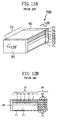
- Figures 12A and 12B illustrate another conventional nitride semiconductor laser device 700 .
- the device 700 includes: n-type GaAlN cladding layer 72 ; InGaN/GaN MQW active layer 76 ; p-type GaAlN cladding layer 75 ; and p-type GaN electrode forming layer 76 , which are stacked in this order on a sapphire substrate 72 by a crystal-growing technique.
- An Ni/Au electrode 77 and a Ti/Al electrode 71 are formed on the upper and lower surfaces of this multilayer structure to form a laser diode 70.
- a reflective layer 90 made up of four pairs of SiO 2 /TiO 2 layers 91 , 92 alternately stacked with the thickness of each layer defined by ⁇ /4n (n is a refractive index of each layer 91 or 92 ), is formed on the rear facet, or the back, of the laser diode 70 .
- an SiO 2 protective layer 80 is formed at a thickness defined by ⁇ /2n (n is a refractive index of the protective layer 80 ).
- ⁇ is an oscillation wavelength of the laser diode 70 .
- the front protective layer 80 and the rear reflective layer 90 are deposited by a sputtering or EB evaporation technique.
- the reflective layer 90 By providing the reflective layer 90 on the back, the reflectance of the back increases to about 98%, and almost all laser light can be emitted from the front. As a result, the operating current can be reduced to about 70% of that consumed by a semiconductor laser device with only an SiO 2 protective layer formed on its back at an ordinary thickness defined by ⁇ /2n.
- the lifetimes of the conventional nitride semiconductor laser devices 600 and 700 are short particularly when operating at high output power.
- the present inventors found that the lifetimes of these nitride semiconductor laser devices are short because of the following reasons:
- An object of the present invention is providing a nitride semiconductor laser device with a much longer lifetime and higher reliability than those of a conventional device.
- a nitride semiconductor laser device includes: a nitride semiconductor laser diode; and a protective layer formed on at least one facet of the nitride semiconductor laser diode.
- the protective Layer is made of Al 1-x-y-z Ga x In y B z N (where 0 ⁇ x, y, z ⁇ 1 and 0 ⁇ x+y+z ⁇ 1), which is transparent to light emitted from the laser diodeIn one embodiment of the present invention, the thickness of the protective layer is preferably N times as large as ⁇ /2n, where N is a positive integer, ⁇ is an oscillation wavelength of the light emitted from the laser diode and n is a refractive index of the protective layer.
- the nitride semiconductor laser diode preferably includes a multiquantum well active layer made up of multiple pairs of In u Ga 1-u N and In v Ga 1-v N (where 0 ⁇ u, v ⁇ 1) layers alternately stacked one upon the other.
- the protective layer is preferably formed by an MOCVD or MBE process.
- the device preferably further includes a reflective layer in contact with the protective layer, the reflective layer reflecting the light emitted from the laser diode.
- the reflective layer is preferably made up of at least one pair of first and second layers, which have mutually different refractive indices and are alternately stacked one upon the other.
- the thicknesses of the first and second layers are preferably defined by ⁇ /4n 1 and ⁇ /4n 2 , respectively, where ⁇ is an oscillation wavelength of the light emitted from the laser diode and n 1 and n 2 are refractive indices of the first or second layers, respectively.
- the thickness of the protective layer may be N times as large as ⁇ /2n, where N is a positive integer, ⁇ is an oscillation wavelength of the light emitted from the laser diode and n is a refractive index of the protective layer.
- the thickness of the protective layer may also be defined by ⁇ /4n,where ⁇ is an oscillation wavelength of the light emitted from the laser diode and n is a refractive index of the protective layer.
- the protective layer may be made of GaN, and the first and second layers may be made of SiO 2 and TiO 2 , respectively, or two types of Al 1- ⁇ - ⁇ - ⁇ Ga ⁇ In ⁇ B ⁇ N (where 0 ⁇ , ⁇ , ⁇ 1 and 0 ⁇ ⁇ + ⁇ + ⁇ ⁇ 1),which have mutually different refractive indices and are transparent to light emitted from the laser diode.
- the reflective layer may further include a third layer between the first and second layers.
- the first, second and third layers are preferably all crystal layers,and a difference in lattice constant between the first and third layers is preferably smaller than a difference in lattice constant between the first and second layers.
- the protective layer is preferably made of GaN
- the reflective layer which is made up of the first, third and second layers stacked in this order, preferably has a GaN/AlGaN/AlN structure.
- the protective layer and the reflective layer are preferably formed by an MOCVD or MBE process.
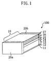
- Figure 1 is a perspective view of a nitride semiconductor laser device 100 , emitting light in the blue region, according to a first embodiment of the present invention.
- the device 100 includes a nitride semiconductor laser diode 10 and a pair of GaN protective layers 20a and 20b , which are provided on both laser facets of the diode 10 .
- the protective layers 20a and 20b are transparent to the light emitted from the laser diode 10 .
- GaN which is the material of the protective layers 20a and 20b , has a band gap larger than that of the optical energy of the radiation emitted from the laser diode 10 .
- the protective layers 20a and 20b are not necessarily made of GaN, but may be made of any other semiconductor material that is transparent to the light emitted from the laser diode 10 .
- the nitride semiconductor laser diode 10 has the following structure.
- An n-type electrode 11 made up of multiple pairs of Ti/Al layers alternately stacked, is formed under an n-type GaN substrate 12 .
- Si-doped n-type Ga 0.9 Al 0.1 N cladding layer 13 Si-doped n-type Ga 0.9 Al 0.1 N cladding layer 13 , MQW active layer 14 , Mg-doped p-type Ga 0.9 Al 0.1 N cladding layer 15 , Mg-doped p-type GaN electrode forming layer 16 and p-type electrode 17 are formed in this order.
- the MQW active layer 14 is made up of multiple pairs of undoped In 0.02 Ga 0.98 N/In 0.15 Ga 0.85 N layers alternately stacked.
- the p-type electrode 17 is made up of multiple pairs of Ni/Au layers alternately stacked.
- the protective layers 20a and 20b are provided on the both facets of the laser diode 10.
- the respective semiconductor layers 13 through 16 are crystal-grown by a metalorganic chemical vapor deposition (MOCVD) technique on the n-type GaN substrate 12 .
- MOCVD metalorganic chemical vapor deposition
- the Si-doped n-type Ga 0.9 Al 0.1 N cladding layer 13 is deposited to be about 0.5 ⁇ m thick on the substrate 12 at a growth temperature of about 1050°C.
- the growth temperature is lowered to about 800 °C, at which the MQW active layer 14 , made up of multiple pairs of undoped In 0.02 Ga 0.98 N/In 0.15 Ga 0.85 N layers alternately stacked, is deposited thereon to be about 0.1 ⁇ m thick (where the thickness of each layer is about 5 nm).
- the growth temperature is raised again to about 1050°C, at which the Mg-doped p-type Ga 0.9 Al 0.1 N cladding layer 15 is deposited thereon to be about 0.5 ⁇ m thick.
- the Mg-doped p-type GaN electrode forming layer 16 is deposited thereon to be about 1 ⁇ m thick with the growth temperature maintained at about 1050°C.
- the substrate 12 is polished until the total thickness of the assembly, including the substrate 12 and the respective semiconductor layers 13 through 16 , reaches about 150 ⁇ m. Thereafter, a p-type electrode 17 , made of multiple pairs of Ni/Au layers alternately stacked, and an n-type electrode 11 , made of multiple pairs of Ti/Al layers alternately stacked, are formed by an evaporation technique on the electrode forming layer 16 and under the substrate 12 , respectively.
- the resulting multilayer structure is cleaved or dry-etched, thereby obtaining the nitride semi-conductor laser diode 10 having the structure of a rectangular parallelepiped with a width of about 500 ⁇ m.
- the GaN protective layers 20a and 20b are formed to be about 0.16 ⁇ m thick on both laser facets of the nitride semiconductor laser diode 10' .
- These layers 20a and 20b are formed by an MOCVD process at a temperature of about 1000°C.
- MOCVD molecular beam epitaxy
- material particles with high kinetic energy do not impact on the laser facets, and the facets are not damaged.
- no lattice defects are caused in the crystals grown on the substrate 12 during the deposition of the protective layers 20a and 20b .
- Similar effects are also attainable if the protective layers 20a and 20b are formed by a molecular beam epitaxy (MBE) process, not the MOCVD process.
- MBE molecular beam epitaxy
- the thermal expansion coefficient of GaN which is the material for the protective layers 20a and 20b , is 3.17 ⁇ 10 -6 K -1 , which is very close to that of the MQW active layer 14 at 3.15 ⁇ 10 -6 K -1 Accordingly, almost no strain is caused due to thermal stress between the MQW active layer 14 and the protective layers 20a and 20b during cooling to room temperature or during the operation of the device.
- the thickness of the protective layers 20a and 20b may be N times as large as ⁇ /2n, where N is a positive integer. In such a case, the oscillation properties of the laser device can be similar to those exhibited when the protective layers 20a and 20b are not formed.
- the thickness of the protective layers 20a and 20b is preferably ⁇ /2n or ⁇ /n.
- the assembly is cut off at a predetermined pitch (e.g., about 400 ⁇ m) to complete the nitride semiconductor laser device 100 having the laser diode 10 with a predetermined size.
- a predetermined pitch e.g., about 400 ⁇ m
- the energy band gap of the GaN protective layers 20a and 20b formed on the laser facets is 3.45 eV, which is larger than the energy (2.95 eV) of the laser light emitted from the MQW active layer 14 (oscillation wavelength: 420 nm). Accordingly, the laser light is not absorbed by the protective layers 20a and 20b but totally transmitted. Also, since the protective layers 20a and 20b are grown without doping, the resistivity of the protective layers 20a and 20b is 10 9 ⁇ ⁇ cm or more. Thus, almost no leakage current flows through the protective layers 20a and 20b .
- Figure 3 illustrates the results of a life test carried out on the blue-light-emitting nitride semiconductor laser device 100 of the first embodiment and the conventional nitride semiconductor laser device 600 including an SiO 2 protective layer shown in Figure 11 . Specifically, Figure 3 illustrates how the rate of variation ⁇ Iop of the operating current changes with time.
- the line E1 represents the results on the nitride semiconductor laser device 100 of the first. embodiment, while the curve C1 illustrates the results on the conventional nitride semiconductor laser device 600 .
- the life test was performed with the operating current controlled under the conditions that the ambient temperature was set at 50°C, the oscillation wavelength was set at 420 nm and the output of the laser was controlled to be constant at 50 mW.
- the rate of variation of the operating current is still constant in the nitride semiconductor laser device 100 of the first embodiment even after the device 100 has operated for 10,000 hours.
- the rate of variation of the operating current abruptly increases on and after the device 600 has operated for 500 hours.
- the lifetime of the nitride semiconductor laser device 100 of the first embodiment is about 20 time longer than that of the conventional nitride semiconductor laser device 600 .
- the protective layers 20a and 20b are made of GaN.
- the protective layers 20a and 20b are preferably made of Al 1-x-y-z Ga x In y B z N (where 0 ⁇ x, y, z ⁇ 1, and 0 ⁇ x+y+z ⁇ 1).
- the mole fractions x, y and z may be selected such that these layers are transparent to the light emitted by the laser diode. Since various nitride semiconductor compounds, containing Al, In and B, are usable for the protective layers 20a and 20b , the range of materials attainable excellent lattice matching can be expanded.
- the protective layers 20a and 20b are preferably made of nitride semiconductor materials in order to establish lattice matching with the nitride semiconductor crystal layers constituting the semiconductor laser diode.
- any other material may also be used so long as the material can establish lattice matching with the nitride semiconductor crystal layers constituting the semiconductor laser diode and have transparency to the oscillation wavelength of the laser diode.
- materials, which show high electrical resistivity and a thermal expansion coefficient close to that of the MQW active layer are preferably used.
- the MQW active layer 14 is also preferably made up of multiple pairs of In u Ga 1-u N/In v Ga 1-v N (where 0 ⁇ u ⁇ 1 and 0 ⁇ v ⁇ 1) layers alternately stacked, for example.
- the structure and the method for producing the semiconductor laser diode 10 are known in the art. Japanese Laid-Open Patent Publication No. 9-219556 is hereby incorporated by reference.
- compositions of the protective layers 20a and 20b and the MQW active layer 14 are defined such that the layers 20a and 20b are transparent to the light emitted from the laser diode as described above.
- the compositions should also be selected such that a difference in lattice constant between the protective layers 20a , 20b and the MQW active layer 14 accounts for about 3% or less of the lattice constant of the MQW active layer 14 . If the difference in lattice constant exceeds 3%, then lattice mismatching happens in the interfaces between the protective layers 20a , 20b and the MQW active layer 14 .
- the protective layers 20a and 20b are sufficiently thick, then the lifetime of the laser may not be shortened even though lattice mismatching of more than 3% has happened. This is because the protective layers 20a and 20b can absorb the strain.
- compositions should also be selected such that a difference in thermal expansion coefficient between the protective layers 20a, 20b and the MQW active layer 14 accounts for about 20% or less of the thermal expansion coefficient of the MQW active layer 14 .
- undoped semiconductor layers are grown as the protective layers 20a and 20b by an MOCVD or MBE process to increase the resistivity of these layers 20a and 20b .
- Group V atoms such as As or P atoms may be implanted thereto at such a level of about 10 15 cm -3 as compensating for nitrogen vacancies existing in the semiconductor layers.
- the resistivity of the protective layers 20a and 20b is preferably equal to or higher than 10 5 ⁇ ⁇ cm, more preferably equal to or higher than 10 9 ⁇ ⁇ cm.
- cladding layers and active layer are formed on an n-type GaN substrate.
- An alternate nitride semiconductor laser diode may include: p-type GaAlN cladding layer; undoped InGaN/InGaN MQW active layer; n-type GaAlN cladding layer; n-type GaN electrode forming layer; and n-type Ti/Al electrode. All of these layers are stacked in this order on a p-type GaN substrate.
- the laser diode further includes a p-type Ni/Au electrode formed under the substrate.
- thin layers of Al 1-x-y-z Ga x In y B z N (where 0 ⁇ x, y, z ⁇ 1, and 0 ⁇ x+y+z ⁇ 1) may be provided as protective layers on the nitride semiconductor laser diode.
- the same effects as those of the first embodiment are also attainable.
- the protective layers 20a and 20b are provided on both facets of the laser diode 10 .
- only one protective layer may be provided on either facet thereof.
- the thickness of the protective layers 20a and 20b does not have to be N times as large as ⁇ /2n, but may be N' times as large as ⁇ /4n (where N' is a positive odd number) such that the light is reflected by the protective layers 20a and 20b which also function as reflective layers.
- Figure 4A is a perspective view of the device 200 of the second embodiment, while Figure 4B is a cross-sectional view thereof taken along the line 4B-4B ' in Figure 4A .
- the device 200 of the second embodiment is different from the device 100 of the first embodiment in that the device 200 further includes a reflective layer 30a on the outer face of the protective layer 20b formed on the back of the semiconductor laser diode 10 . Also, in the device 200 of the second embodiment, the respective thicknesses of the protect tive layers 20a and 20b , formed on the front (light-emitting face) and the back of the semiconductor laser diode 10 , are about 0.08 ⁇ m and about 0.16 ⁇ m, respectively. In the other respects, the structure of the device 200 is substantially the same as that of the device 100 . Thus, the elements with substantially the same functions are identified by the same reference numerals and the detailed description thereof will be omitted herein.
- the reflective layer 30a of the device 200 is formed by alternately stacking eight pairs of nitride semiconductor layers with mutually different refractive indices, e.g., AlN layers 31 (thickness: about 0.05 ⁇ m) and GaN layers 32 (thickness: about 0.04 ⁇ m).
- the thickness of each of these nitride semiconductor layers 31 and 32 is represented by ⁇ /4n, where ⁇ is an oscillation wavelength of the laser diode (e.g., 420 nm) and n is a refractive index of each layer 31 or 32 .
- the reflectance at the back is about 93%.
- the resistivity thereof is 10 9 ⁇ ⁇ cm or more. Accordingly, no leakage current flows through these nitride semiconductor layers 31 and 32 .
- the nitride semiconductor laser device 200 is fabricated in the following manner. First, the semiconductor later diode 10' is formed as shown in Figure 2B as in the first embodiment.
- the GaN protective layer 20b is formed to be about 0.16 ⁇ m thick on the back of the laser diode 10' .
- the interface between the protective layer 20b and the AlN layer 31 formed thereon serves as a facet of the laser cavity. That is to say, since the length of the cavity increases only by the thickness of the protective layer 20b , the oscillation properties of the laser diode, such as the operating current thereof, are hardly affected if the thickness of the protective layer 20b is variable to a certain degree.
- the eight pairs of nitride semiconductor layers of the two types namely, the AlN layers 31 (thickness: about 0.05 ⁇ m) and the GaN layers 32 (thickness: about 0.04 ⁇ m), are alternately stacked on the protective layer 20b , thereby forming the reflective layer 30a thereon.
- the thickness of each of the AlN layers 31 and the GaN layers 32 are represented by ⁇ /4n, where ⁇ is the oscillation wavelength of the laser diode (e.g., 420 nm) and n is the refractive index of each AlN or GaN layer 31 or 32 (i.e., 2.0 and 2.6, respectively).
- the reflectance at the back of the semiconductor laser diode 10' is about 93%.
- the resistivity thereof is 10 9 ⁇ ⁇ cm or more. Accordingly, no leakage current flows through the AlN and GaN layers 31 , 32 .
- the GaN protective layer 20a is formed on the front of the semiconductor laser diode 10'.
- the thickness of the protective layer 20a is set at about 0.08 ⁇ m, which is also defined by ⁇ /2n. It is noted that the protective layer 20b and the reflective layer 30a may be deposited on the back of the semiconductor laser diode 10' after the protective layer 20a has been deposited on the front of the laser diode 10' .
- the resultant multilayer structure is cleaved at a pitch of about 400 ⁇ m as in the first embodiment.
- the nitride semiconductor laser device 200 of the second embodiment having the laser diode 10 with a predetermined size is completed.
- the lifetime of the semiconductor laser device can be extended as in the first embodiment.
- a high reflectance is also attained.
- the reflective layer 30a is preferably made of Al 1-x-y-z Ga x In y B z N (where 0 ⁇ x, y, z ⁇ 1, and 0 ⁇ x+y +z ⁇ 1).
- the mole fractions x, y and z may be selected such that the reflective layer is transparent to the light emitted from the laser diode.
- Figure 5 illustrates a cross section of a nitride semiconductor laser device 300 according to a third embodiment of the present invention.
- the device 300 of the third embodiment is different from the device 200 of the second embodiment in the structure of a reflective layer 30b .
- the structure of the device 300 is substantially the same as that of the device 200.
- the elements with substantially the same functions are identified by the same reference numerals and the detailed description thereof will be omitted herein.
- the reflective layer 30b of the nitride semiconductor laser device 300 is formed by alternately stacking five pairs of insulating layers of two types, namely, SiO 2 layers 33 and TiO 2 layers 34 , on the GaN protective layer 20b provided on the back of the laser diode 10 .
- the thickness of each of these layers 33 and 34 is represented by ⁇ /4n, where ⁇ is the oscillation wavelength of the laser diode and n is a refractive index of each layer 33 or 34 .
- the protective layer 20a with a thickness defined by ⁇ /2n is formed on the front of the laser diode 10 .
- the five pairs of insulating layers of the two types with mutually different refractive indices namely, the SiO 2 layers 33 (thickness: about 0.07 ⁇ m) and the TiO 2 layers 34 (thickness: about 0.04 ⁇ m), are alternately stacked on the protective layer 20b.
- the thickness of each of these layers 33 and 34 is represented by ⁇ /4n, where ⁇ is the oscillation wavelength of the laser diode (e.g., 420 nm).
- ⁇ is the oscillation wavelength of the laser diode (e.g., 420 nm).
- these SiO 2 and TiO 2 layers 33 and 34 are formed on the protective layer 20b, and do not directly affect the facet of the active layer 14 in the semiconductor laser diode 10' during the deposition process thereof. Accordingly, these SiO 2 and TiO 2 layers 33 and 34 may be formed by a sputtering or EB evaporation technique. However,in order to minimize the damage done to the crystal layers in the semiconductor laser diode 10' ,these SiO 2 and TiO 2 layers 33 and 34 are preferably grown by an MBE technique.
- ⁇ /2n e.g. 0.08 ⁇ m
- the lifetime of the semiconductor laser device can be extended as in the first embodiment and a high reflectance is attained as well.
- Figure 6 illustrates a cross section of a nitride semiconductor laser device 400 according to a fourth embodiment of the present invention.
- the device 400 of the fourth embodiment is different from the device 200 of the second embodiment in the structure of a protective layer 20c formed on the back of the semiconductor laser diode 10 .
- the structure of the device 400 is substantially the same as that of the device 200 .
- the elements with substantially the same functions are identified by the same reference numerals and the detailed description thereof will be omitted herein.
- the GaN protective layer 20c formed on the back of the laser diode 10 has a thickness defined by ⁇ /4n, where ⁇ is the oscillation wavelength of the laser diode and n is a refractive index of the protective layer 20c .
- a reflective layer 30a is also formed on the protective layer 20c by alternately stacking thereon eight pairs of nitride semiconductor layers of two types, namely, AlN layers 31 and GaN layers 32 . The thickness of each of these layers 31 and 32 is also defined by ⁇ /4n.
- the GaN protective layer 20a with a thickness defined by ⁇ /2n is formed on the front of the semiconductor laser diode 10 .
- the protective layer 20c of the device 400 serves as a reflective layer, the reflectance at the back of the device 400 is higher than the device 200 of the second embodiment. As a result, a reflectance as high as about 95% is attained in this embodiment.
- the thickness of the protective layer 20c is not necessarily defined by ⁇ /4n, but may be N' times as large as ⁇ /4n, where N' is a positive odd number. In view of the productivity, the thickness of the protective layer 20c is preferably ⁇ /4n.
- Figure 7 illustrates the results of a life test carried out on the devices 200 , 400 ( E2 in Figure 7 ) and 300 ( E3 in Figure 7 ) of the second, third and fourth embodiments and the conventional device 700 ( C2 in Figure 7 ) illustrated in Figures 12A and 12B .
- Figure 7 illustrates how the rates of variation ⁇ Iop of the operating current change in the respective devices with time at a temperature of 50°C and an output power of 50 mW.
- the lifetime of the semiconductor laser device can be extended as in the first embodiment, and an even higher reflectance is attained as well.
- Figure 8 illustrates a cross section of a nitride semiconductor laser device 500 according to a fifth embodiment of the present invention.
- the device 500 of the fifth embodiment is different from the device 200 of the second embodiment in the structure of a reflective layer 40 formed on the back of the semiconductor laser diode 10.
- the structure of the device 500 is substantially the came as that of the device 200 .
- the elements with substantially the same functions are identified by the same reference numerals and the detailed description thereof will be omitted herein.
- 16 sets of multilayer structures each consisting of: Al 0.5 Ga 0 . 5 N layer 41 (thickness: 0.01 ⁇ m); AlN layer 42 (thickness: 0.03 ⁇ m); Al 0.5 Ga 0.5 N layer 41 (thickness: 0.01 ⁇ m); and GaN layer 43 (thickness: 0.04 ⁇ m), are stacked on the GaN protective layer 20b formed on the back of the semiconductor laser diode 10 .
- the GaN protective layer 20a with a thickness defined by ⁇ /2n is formed on the front of the laser diode 10 .
- n is formed on the front of the laser diode 10 .
- nitride semiconductor layers 41 , 42 and 43 are preferably made of Al 1-x-y-z Ga x B z N (where 0 ⁇ x, y, z ⁇ 1, and 0 ⁇ x+y+z ⁇ 1).
- the mole fractions x, y and z may be selected such that these layers are transparent to the light emitted from the laser diode.
- the lattice constants and thermal expansion coefficients of these layers should preferably be matched with each other and the electrical resistivity of these layers should preferably be high.
- the respective thicknesses of the Al 0.5 Ga 0.5 N 41 /AlN 42 /Al 0.5 Ga 0.5 N 41 /GaN 43 layers are defined by ⁇ /20n, 3 ⁇ /20n, ⁇ /20n and ⁇ /4n, where ⁇ is the oscillation wavelength of the laser diode and n is a refractive index of each of these layers.
- the thickness of the Al 0.5 Ga 0.5 N layer 41 is not limited to ⁇ /20n so long as the total thickness of the Al 0.5 Ga 0.5 N 41 /AlN 42 /Al 0.5 Ga 0.5 N 41 layers is ⁇ /4n.
- the reflectance at the back of the laser cavity can be as high as about 99%.
- the respective nitride semiconductor layers, included in the reflective layer 40 are grown without doping, the resistivity of each layer is 10 9 ⁇ ⁇ cm or more. Thus, almost no leakage current flows through the reflective layer 40 .
- a GaN protective layer 20a with a thickness defined by ⁇ /2n (e.g., 0.08 ⁇ m) is formed on the front of the semiconductor laser diode 10' .
- Figure 9 illustrates a relationship between a wavelength at the reflective layer 40 and an associated calculated reflectance at the facet. As shown in Figure 9 , the reflectance reaches as high as 99% when the wavelength is 420 nm.
- the number of layers included in the multilayer reflective layer 40 may be appropriately selected to attain a required reflectance.
- a substantially equal reflectance is attainable if at least one two-layered structure consisting of AlN layer 42 and GaN layer 43 , each having a thickness defined by ⁇ /4n (e.g., 0.05 ⁇ m and 0.04 ⁇ m), is formed periodically instead of the reflective layer 40 .
- the difference in lattice constant is slightly less than 2% at room temperature.
- the AlN layer 42 is particularly likely to be strained due to tensile strain applied thereto.
- an Al 0.5 Ga 0.5 N layer 41 with a lattice constant intermediate between those of the AlN and GaN layers 42 and 43 should be inserted between the AlN and GaN layers 42 and 43 . In such a case, the lifetime of the semiconductor laser device can be further extended.
- multiple Al q Ga 1-q As layers may be inserted instead of the Al 0.5 Ga 0.5 N layer 41 between the AlN and GaN layers 42 and 43 or multiple layers, where the value of q continuously changes from 0 to 1, may be formed therebetween.
- the GaN protective layer 20b formed on the back of the semiconductor laser diode 10 , is omitted from the nitride semiconductor laser device 500 of the fifth embodiment.
- 16 sets of four-layered structures each consisting of: Al 0.5 Ga 0.5 N layer 41 (thickness: 0.01 ⁇ m); AlN layer 42 (thickness: 0.03 ⁇ m); Al 0.5 Ga 0.5 N layer 41 (thickness: 0.01 ⁇ m); and GaN layer 43 (thickness: 0.04 ⁇ m), are stacked directly on the back of the laser diode 10 .
- a reflective layer with a high reflectance can also be attained.
- an In 0.02 Ga 0.98 N layer may be formed as a substitute protective layer directly on the back of the semiconductor laser diode 10.
- the protective layer may have a thickness N' times as large as ⁇ /4n (where N' is a positive odd number) to function as a reflective layer.
- Figure 10 illustrates the results of a life test carried out on the nitride semiconductor laser devices of the fifth and sixth embodiments ( E4 and E5 in Figure 10 ) and the conventional nitride semiconductor laser device 700 illustrated in Figures 12A and 12B ( C3 in Figure 10 ). Specifically, Figure 10 illustrates how the rates of variation ⁇ Iop of the operating current change in the respective devices with time at a temperature of 50°C and an output power of 50 mW.
- the lifetime of the semiconductor laser device can be extended as in the first embodiment, and an even higher reflectance is attained as well.
- undoped layers may be formed by an MOCVD or MBE process.
- Group V atoms such as As or P atoms may be implanted thereto at such a level of about 10 15 cm -3 as compensating for nitrogen vacancies existing in the conductive layers.
- a third layer should be inserted therebetween to reduce the difference in lattice constant between these two layers.
- a reflective layer can be formed substantially without straining the active layer.
- these layers are formed by an MOCVD or MBE process, then the damage done to the laser facets during the deposition process can be drastically reduced.
- the strain at room temperature can also be relaxed.
- a reflective layer is supposed to be formed only on the rear facet of each semiconductor laser diode. If a low threshold voltage should be attained at the expense of the output power of the laser, however, another reflective layer may be provided on the light-emitting end of the laser diode. In such a case, the reflectance of each reflective layer may be appropriately set depending on the applications thereof.
- the present invention provides a nitride semiconductor laser device with a long lifetime, which can operate reliably enough not only when the output power thereof is low, but also even when the output power is too high for a conventional device to operate normally due to strain or defects.
- the nitride semiconductor laser device of the present invention is applicable as a blue-light-emitting laser device to a compact disk reproducing system and so on.
Abstract
Description
- The present invention relates to a nitride semiconductor laser device.
- A semiconductor laser device using a nitride semiconductor such as GaN, InN or AlN can generate light in the green to blue regions and is expected to be a light source for a high-density optical disk apparatus. A nitride semiconductor laser device of the type emitting light in the blue part of the spectrum will be described as an exemplary prior art device.
- Figure 11 illustrates a conventional nitride
semiconductor laser device 600. In thedevice 600, n-type GaN electrode forming layer 62 (including upper andlower parts GaAlN cladding layer 63, InGaN/GaN multi-quantum well (MQW)active layer 64, p-typeGaAlN cladding layer 65 and p-type GaNelectrode forming layer 66 are formed in this order on asapphire substrate 61. An electrode provided on the n-type side (n-type electrode) 67, made up of multiple pairs of Ti/Al layers alternately stacked, is formed on thelower part 62a of the n-typeelectrode forming layer 62. On the other hand, an electrode provided on the p-type side (p-type electrode) 68, made up of multiple pairs of Ni/Au layers alternately stacked, is formed on the p-typeelectrode forming layer 66. In this manner, alaser diode 60, also called a "laser element or cavity" is formed. On both facets of thelaser diode 60, from/by which laser light is emitted or reflected, a pair of SiO2 or SiNprotective layers 69 are provided, thus preventing the deterioration of the laser facets. In this case, SiO2 or SiN need not have their compositions exactly defined by stoichiometry. Instead, theselayers 69 should have resistivity (or insulating properties) and refractive index that are substantially equal to those of SiO2 or SiN. In this specification, part of a semiconductor laser device, from which stimulated emission of radiation is produced, will be referred to as a "semiconductor laser diode", and a combination of the semiconductor laser diode with at least one protective or reflective layer a "semiconductor laser device" for convenience. - The conventional nitride
semiconductor laser device 600 may be fabricated by the following method. First, theelectrode forming layer 62,cladding layer 63, MQWactive layer 64,cladding layer 65 andelectrode forming layer 66 are formed in this order by a crystal-growing technique on thesapphire substrate 61. Thereafter, respective portions of theelectrode forming layer 66,cladding layer 65, MQWactive layer 64,cladding layer 63 andupper part 62b of theelectrode forming layer 62 are etched, thereby exposing the upper surface of thelower part 62a of theelectrode forming layer 62. The n- and p-type electrodes 67 and 68 are formed on the exposed upper surface of theelectrode forming layer 62a and theelectrode forming layer 66, respectively, by an evaporation technique. Thereafter, the pair ofprotective layers 69 are formed on both laser facets by a sputtering or electron beam (EB) evaporation technique. - Figures 12A and 12B illustrate another conventional nitride
semiconductor laser device 700. Thedevice 700 includes: n-typeGaAlN cladding layer 72; InGaN/GaN MQWactive layer 76; p-typeGaAlN cladding layer 75; and p-type GaNelectrode forming layer 76, which are stacked in this order on asapphire substrate 72 by a crystal-growing technique. An Ni/Au electrode 77 and a Ti/Al electrode 71 are formed on the upper and lower surfaces of this multilayer structure to form alaser diode 70. In order to reduce the operating current of thislaser diode 70, areflective layer 90, made up of four pairs of SiO2/TiO2 layers 91, 92 alternately stacked with the thickness of each layer defined by λ/4n (n is a refractive index of eachlayer 91 or 92), is formed on the rear facet, or the back, of thelaser diode 70. On the front facet, or the front, of thelaser diode 70, an SiO2protective layer 80 is formed at a thickness defined by λ/2n (n is a refractive index of the protective layer 80). Herein, λ is an oscillation wavelength of thelaser diode 70. The stimulated emission of radiation in output from the front. The frontprotective layer 80 and the rearreflective layer 90 are deposited by a sputtering or EB evaporation technique. - By providing the
reflective layer 90 on the back, the reflectance of the back increases to about 98%, and almost all laser light can be emitted from the front. As a result, the operating current can be reduced to about 70% of that consumed by a semiconductor laser device with only an SiO2 protective layer formed on its back at an ordinary thickness defined by λ/2n. - However, the lifetimes of the conventional nitride
semiconductor laser devices - (1) The
laser diodes protective layers reflective layer 90, formed on the facets thereof are formed of SiO2 or TiO2 and are all amorphous layers. In addition, the length of a bond in the material for these amorphous layers (e.g., the length of an Si-O bond) is different from the lattice constant of the crystal layers in the laser diodes. Accordingly, lattice mismatching is caused in these interfaces to create lattice defects in these crystal layers (in the MQW active layer, in particular). Moreover, if theprotective layers reflective layer 90 are formed on the laser facets by a sputtering or EB evaporation technique, then these laser facets would be damaged due to relatively high impact energy of material particles flying from the target. AS a result, lattice defects might be caused in the crystal layers in thelaser diodes - (2) The thermal expansion coefficients of the crystal
layers in the
laser diodes protective layers reflective layer 90. Accordingly, the crystal layers (the MQW active layer, in particular) are strained while theprotective layers reflective layer 90 are cooled down to room temperature after these layers have been formed and during the operation of the devices (during high-power operation, in particular). As a result, crystal defects are newly created or the number thereof increases. For example, the thermal expansion coefficient of the MQWactive layer 64 is 3.15 × 10⁻⁶ K-1, which is greatly different from that of theprotective layer 69 at 1.6×10⁻⁷ K-1. -
- An object of the present invention is providing a nitride semiconductor laser device with a much longer lifetime and higher reliability than those of a conventional device.
- A nitride semiconductor laser device according to the present invention includes: a nitride semiconductor laser diode; and a protective layer formed on at least one facet of the nitride semiconductor laser diode. The protective Layer is made of Al1-x-y-zGaxInyBzN (where 0≦x, y, z≦1 and 0≦x+y+z≦ 1), which is transparent to light emitted from the laser diodeIn one embodiment of the present invention, the thickness of the protective layer is preferably N times as large as λ/2n, where N is a positive integer, λ is an oscillation wavelength of the light emitted from the laser diode and n is a refractive index of the protective layer.
- In another embodiment of the present invention, the nitride semiconductor laser diode preferably includes a multiquantum well active layer made up of multiple pairs of InuGa1-uN and InvGa1-vN (where 0 ≦ u, v ≦ 1) layers alternately stacked one upon the other.
- In still another embodiment, the protective layer is preferably formed by an MOCVD or MBE process.
- In yet another embodiment, the device preferably further includes a reflective layer in contact with the protective layer, the reflective layer reflecting the light emitted from the laser diode.
- In that embodiment, the reflective layer is preferably made up of at least one pair of first and second layers, which have mutually different refractive indices and are alternately stacked one upon the other.
- Specifically, the thicknesses of the first and second layers are preferably defined by λ/4n1 and λ/4n2, respectively, where λ is an oscillation wavelength of the light emitted from the laser diode and n1 and n2 are refractive indices of the first or second layers, respectively.
- In an alternate embodiment, the thickness of the protective layer may be N times as large as λ/2n, where N is a positive integer, λ is an oscillation wavelength of the light emitted from the laser diode and n is a refractive index of the protective layer.
- In another alternate embodiment, the thickness of the protective layer may also be defined by λ/4n,where λ is an oscillation wavelength of the light emitted from the laser diode and n is a refractive index of the protective layer.
- In another embodiment, the protective layer may be made of GaN, and the first and second layers may be made of SiO2 and TiO2, respectively, or two types of Al1-α-β-γGaαInβBγN (where 0≦α, β, γ≦1 and 0 ≦ α+β+γ ≦ 1),which have mutually different refractive indices and are transparent to light emitted from the laser diode.
- In still another embodiment, the reflective layer may further include a third layer between the first and second layers. The first, second and third layers are preferably all crystal layers,and a difference in lattice constant between the first and third layers is preferably smaller than a difference in lattice constant between the first and second layers.
- In yet another embodiment, the protective layer is preferably made of GaN, and the reflective layer, which is made up of the first, third and second layers stacked in this order, preferably has a GaN/AlGaN/AlN structure.
- In yet another embodiment, the protective layer and the reflective layer are preferably formed by an MOCVD or MBE process.
-
- Figure 1 is a perspective view of a nitride semiconductor laser device according to a first embodiment of the present invention.
- Figures 2A through 2D are perspective views illustrating respective process steps for fabricating the nitride semiconductor laser device of the first embodiment.
- Figure 3 is a graph illustrating the results of a life test carried out on the nitride semiconductor laser device of the first embodiment and a conventional nitride semiconductor laser device.
- Figure 4A is a perspective view of a nitride semiconductor laser device according to a second embodiment of the present invention; and
- Figure 4B in a cross-sectional view of the device taken
along the
line 4B-4B' in Figure 4A. - Figure 5 is a cross-sectional view of a nitride semiconductor laser device according to a third embodiment of the present invention.
- Figure 6 is a cross-sectional view of a nitride semiconductor laser device according to a fourth embodiment of the present invention.
- Figure 7 is a graph illustrating the results of a life test carried out on the nitride semiconductor laser devices of the second, third and fourth embodiments and a conventional nitride semiconductor laser device.
- Figure 8 is a cross-sectional view of a nitride semiconductor laser device according to a fifth embodiment of the present invention.
- Figure 9 is a graph illustrating a relationship between a wavelength at the reflective layer and a calculated reflectance at the facet in the nitride semiconductor laser device of the fifth embodiment.
- Figure 10 is a graph illustrating the results of a life test carried out on the nitride semiconductor laser devices of the fifth and sixth embodiments and the conventional nitride semiconductor laser device.
- Figure 11 in a perspective view illustrating a conventional nitride semiconductor laser device.
- Figure 12A is a perspective view illustrating another conventional nitride semiconductor laser device; and
- Figure 12B is a cross-sectional view of the nitride semiconductor laser device shown in Figure 12A.
-
- Figure 1 is a perspective view of a nitride
semiconductor laser device 100, emitting light in the blue region, according to a first embodiment of the present invention. - The
device 100 includes a nitridesemiconductor laser diode 10 and a pair of GaNprotective layers diode 10. Theprotective layers laser diode 10. In other words, GaN, which is the material of theprotective layers laser diode 10. Theprotective layers laser diode 10. - The nitride
semiconductor laser diode 10 has the following structure. An n-type electrode 11, made up of multiple pairs of Ti/Al layers alternately stacked, is formed under an n-type GaN substrate 12. On thesubstrate 12, Si-doped n-type Ga0.9Al0.1N cladding layer 13, MQWactive layer 14, Mg-doped p-type Ga0.9Al0.1N cladding layer 15, Mg-doped p-type GaNelectrode forming layer 16 and p-type electrode 17 are formed in this order. The MQWactive layer 14 is made up of multiple pairs of undoped In0.02Ga0.98N/In0.15Ga0.85N layers alternately stacked. And the p-type electrode 17 is made up of multiple pairs of Ni/Au layers alternately stacked. Theprotective layers laser diode 10. - Hereinafter, a method for fabricating this blue-light-emitting nitride
semiconductor laser device 100 will be described with reference to Figures 2A, 2B, 2C and 2D. - First, as shown in Figure 2A, the respective semiconductor layers 13 through 16 are crystal-grown by a metalorganic chemical vapor deposition (MOCVD) technique on the n-
type GaN substrate 12. - Specifically, the Si-doped n-type Ga0.9Al0.1
N cladding layer 13 is deposited to be about 0.5 µm thick on thesubstrate 12 at a growth temperature of about 1050°C. Next, the growth temperature is lowered to about 800 °C, at which the MQWactive layer 14, made up of multiple pairs of undoped In0.02Ga0.98N/In0.15Ga0.85N layers alternately stacked, is deposited thereon to be about 0.1 µm thick (where the thickness of each layer is about 5 nm). Then, the growth temperature is raised again to about 1050°C, at which the Mg-doped p-type Ga0.9Al0.1N cladding layer 15 is deposited thereon to be about 0.5 µm thick. Subsequently, the Mg-doped p-type GaNelectrode forming layer 16 is deposited thereon to be about 1 µm thick with the growth temperature maintained at about 1050°C. - Next, as shown in Figure 2B, the
substrate 12 is polished until the total thickness of the assembly, including thesubstrate 12 and the respective semiconductor layers 13 through 16, reaches about 150 µm. Thereafter, a p-type electrode 17, made of multiple pairs of Ni/Au layers alternately stacked, and an n-type electrode 11, made of multiple pairs of Ti/Al layers alternately stacked, are formed by an evaporation technique on theelectrode forming layer 16 and under thesubstrate 12, respectively. The resulting multilayer structure is cleaved or dry-etched, thereby obtaining the nitridesemi-conductor laser diode 10 having the structure of a rectangular parallelepiped with a width of about 500 µm. - Then, as shown in Figure 2C, the GaN
protective layers layers substrate 12 during the deposition of theprotective layers protective layers - The thermal expansion coefficient of GaN, which is the material for the
protective layers active layer 14 at 3.15×10⁻⁶ K-1 Accordingly, almost no strain is caused due to thermal stress between the MQWactive layer 14 and theprotective layers - Supposing the refractive index n of GaN is 2.6 and the laser oscillation wavelength λ is 420 nm, the thickness of the
protective layers protective layers protective layers protective layers - Finally, as shown in Figure 2D, the assembly is cut off at a predetermined pitch (e.g., about 400 µm) to complete the nitride
semiconductor laser device 100 having thelaser diode 10 with a predetermined size. - In this embodiment, the energy band gap of the GaN
protective layers protective layers protective layers protective layers protective layers - Figure 3 illustrates the results of a life test carried out on the blue-light-emitting nitride
semiconductor laser device 100 of the first embodiment and the conventional nitridesemiconductor laser device 600 including an SiO2 protective layer shown in Figure 11. Specifically, Figure 3 illustrates how the rate of variation ΔIop of the operating current changes with time. In Figure 3, the line E1 represents the results on the nitridesemiconductor laser device 100 of the first. embodiment, while the curve C1 illustrates the results on the conventional nitridesemiconductor laser device 600. The life test was performed with the operating current controlled under the conditions that the ambient temperature was set at 50°C, the oscillation wavelength was set at 420 nm and the output of the laser was controlled to be constant at 50 mW. - As shown in Figure 3, the rate of variation of the operating current is still constant in the nitride
semiconductor laser device 100 of the first embodiment even after thedevice 100 has operated for 10,000 hours. In contrast, in the conventional nitridesemiconductor laser device 600, the rate of variation of the operating current abruptly increases on and after thedevice 600 has operated for 500 hours. As can be seen, the lifetime of the nitridesemiconductor laser device 100 of the first embodiment is about 20 time longer than that of the conventional nitridesemiconductor laser device 600. Analyzing these results, it is believed that such a long lifetime is attained according to the present invention because deterioration of the laser facets can be suppressed by the GaNprotective layers active layer 14. - In this embodiment, the
protective layers protective layers protective layers - As just described, the
protective layers - The MQW
active layer 14 is also preferably made up of multiple pairs of InuGa1-uN/InvGa1-vN (where 0≦u≦1 and 0≦v≦1) layers alternately stacked, for example. The structure and the method for producing thesemiconductor laser diode 10 are known in the art. Japanese Laid-Open Patent Publication No. 9-219556 is hereby incorporated by reference. - The respective compositions of the
protective layers active layer 14 are defined such that thelayers protective layers active layer 14 accounts for about 3% or less of the lattice constant of the MQWactive layer 14. If the difference in lattice constant exceeds 3%, then lattice mismatching happens in the interfaces between theprotective layers active layer 14. As a result, lattice defects are caused in the MQWactive layer 14 and the lifetime of the nitride semiconductor laser device is sometimes shortened. It should be noted that if theprotective layers protective layers - In addition, the compositions should also be selected such that a difference in thermal expansion coefficient between the
protective layers active layer 14 accounts for about 20% or less of the thermal expansion coefficient of the MQWactive layer 14. - In this embodiment, undoped semiconductor layers are grown as the
protective layers layers protective layers protective layers protective layers - In the foregoing embodiment, cladding layers and active layer are formed on an n-type GaN substrate. An alternate nitride semiconductor laser diode may include: p-type GaAlN cladding layer; undoped InGaN/InGaN MQW active layer; n-type GaAlN cladding layer; n-type GaN electrode forming layer; and n-type Ti/Al electrode. All of these layers are stacked in this order on a p-type GaN substrate. The laser diode further includes a p-type Ni/Au electrode formed under the substrate. And thin layers of Al1-x-y-zGaxInyBzN (where 0≦x, y, z≦ 1, and 0≦x+y+z≦1) may be provided as protective layers on the nitride semiconductor laser diode. In such an alternate embodiment, the same effects as those of the first embodiment are also attainable.
- In this embodiment, the
protective layers laser diode 10. Alternatively, only one protective layer may be provided on either facet thereof. The thickness of theprotective layers protective layers - The alternate protective layer materials and the substitute laser diode structure described above arc also applicable to the following embodiments.
- Next, a nitride
semiconductor laser device 200 according to a second embodiment of the present invention will be described with reference to Figures 4A and 4B. Figure 4A is a perspective view of thedevice 200 of the second embodiment, while Figure 4B is a cross-sectional view thereof taken along theline 4B-4B' in Figure 4A. - The
device 200 of the second embodiment is different from thedevice 100 of the first embodiment in that thedevice 200 further includes areflective layer 30a on the outer face of theprotective layer 20b formed on the back of thesemiconductor laser diode 10. Also, in thedevice 200 of the second embodiment, the respective thicknesses of theprotect tive layers semiconductor laser diode 10, are about 0.08 µm and about 0.16 µm, respectively. In the other respects, the structure of thedevice 200 is substantially the same as that of thedevice 100. Thus, the elements with substantially the same functions are identified by the same reference numerals and the detailed description thereof will be omitted herein. - The
reflective layer 30a of thedevice 200 is formed by alternately stacking eight pairs of nitride semiconductor layers with mutually different refractive indices, e.g., AlN layers 31 (thickness: about 0.05 µm) and GaN layers 32 (thickness: about 0.04 µm). The thickness of each of these nitride semiconductor layers 31 and 32 is represented by λ/4n, where λ is an oscillation wavelength of the laser diode (e.g., 420 nm) and n is a refractive index of eachlayer 31 or 32. As a result, the reflectance at the back is about 93%. Also, since these nitride semiconductor layers 31 and 32 are undoped semiconductor layers, the resistivity thereof is 109 Ω · cm or more. Accordingly, no leakage current flows through these nitride semiconductor layers 31 and 32. - The nitride
semiconductor laser device 200 is fabricated in the following manner. First, the semiconductor later diode 10' is formed as shown in Figure 2B as in the first embodiment. - Next, as in the first embodiment, the GaN
protective layer 20b is formed to be about 0.16 µm thick on the back of the laser diode 10'. Theprotective layer 20b is formed by an MOCVD process at about 1000 °C, which is slightly lower than the growth temperature of the semiconductor laser diode (with a double heterostructure). This thickness is set at twice as large as λ/2n=0.08 µm, where the refractive index n of GaN is 2.6 and the oscillation wavelength λ of the laser diode is 420 nm. It should be noted, however, that the thickness of theprotective layer 20b does not have be exactly twice of λ/2n. This is because the interface between theprotective layer 20b and theAlN layer 31 formed thereon serves as a facet of the laser cavity. That is to say, since the length of the cavity increases only by the thickness of theprotective layer 20b, the oscillation properties of the laser diode, such as the operating current thereof, are hardly affected if the thickness of theprotective layer 20b is variable to a certain degree. - Next, the eight pairs of nitride semiconductor layers of the two types, namely, the AlN layers 31 (thickness: about 0.05 µm) and the GaN layers 32 (thickness: about 0.04 µm), are alternately stacked on the
protective layer 20b, thereby forming thereflective layer 30a thereon. The thickness of each of the AlN layers 31 and the GaN layers 32 are represented by λ/4n, where λ is the oscillation wavelength of the laser diode (e.g., 420 nm) and n is the refractive index of each AlN orGaN layer 31 or 32 (i.e., 2.0 and 2.6, respectively). As a result, the reflectance at the back of the semiconductor laser diode 10' is about 93%. Also, since these AlN and GaN layers 31 and 32 have been grown without doping, the resistivity thereof is 109 Ω · cm or more. Accordingly, no leakage current flows through the AlN and GaN layers 31, 32. - Subsequently, as in the first embodiment, the GaN
protective layer 20a is formed on the front of the semiconductor laser diode 10'. In this embodiment, the thickness of theprotective layer 20a is set at about 0.08 µm, which is also defined by λ/2n. It is noted that theprotective layer 20b and thereflective layer 30a may be deposited on the back of the semiconductor laser diode 10' after theprotective layer 20a has been deposited on the front of the laser diode 10'. - Finally, the resultant multilayer structure is cleaved at a pitch of about 400 µm as in the first embodiment. In this manner, the nitride
semiconductor laser device 200 of the second embodiment having thelaser diode 10 with a predetermined size is completed. - According to the second embodiment, the lifetime of the semiconductor laser device can be extended as in the first embodiment. In addition, a high reflectance is also attained.
- It should be noted that various other nitride semiconductor compounds are usable for the
reflective layer 30a, as well as for theprotective layers reflective layer 30a is preferably made of Al1-x-y-zGaxInyBzN (where 0≦x, y, z≦1, and 0≦x+y +z≦1). The mole fractions x, y and z may be selected such that the reflective layer is transparent to the light emitted from the laser diode. The same statement applies to the following embodiments. - Figure 5 illustrates a cross section of a nitride
semiconductor laser device 300 according to a third embodiment of the present invention. Thedevice 300 of the third embodiment is different from thedevice 200 of the second embodiment in the structure of areflective layer 30b. In the other respects, the structure of thedevice 300 is substantially the same as that of thedevice 200. Thus, the elements with substantially the same functions are identified by the same reference numerals and the detailed description thereof will be omitted herein. - The
reflective layer 30b of the nitridesemiconductor laser device 300 is formed by alternately stacking five pairs of insulating layers of two types, namely, SiO2 layers 33 and TiO2 layers 34, on the GaNprotective layer 20b provided on the back of thelaser diode 10. The thickness of each of theselayers layer protective layer 20a with a thickness defined by λ/2n is formed on the front of thelaser diode 10. - Hereinafter, a method for fabricating this nitride
semiconductor laser device 300 will be briefly described. The same process steps as those of the second embodiment are performed until theprotective layer 20b is formed to be about 0.16 µm thick on the back of the laser diode 10' as shown in Figure 2C. - Next, the five pairs of insulating layers of the two types with mutually different refractive indices, namely, the SiO2 layers 33 (thickness: about 0.07 µm) and the TiO2 layers 34 (thickness: about 0.04 µm), are alternately stacked on the
protective layer 20b. The thickness of each of theselayers laser diode 10 is about 98%. Also, these SiO2 and TiO2 layers 33 and 34 are formed on theprotective layer 20b, and do not directly affect the facet of theactive layer 14 in the semiconductor laser diode 10' during the deposition process thereof. Accordingly, these SiO2 and TiO2 layers 33 and 34 may be formed by a sputtering or EB evaporation technique. However,in order to minimize the damage done to the crystal layers in the semiconductor laser diode 10',these SiO2 and TiO2 layers 33 and 34 are preferably grown by an MBE technique. - Thereafter, a GaN
protective layer 20a with a thickness defined by λ/2n (e.g., 0.08 µm)is formed on the front of the semiconductor laser diode 10'. By performing the same process steps as those of the second embodiment after that, the nitridesemiconductor laser device 300 is completed. - According to the third embodiment, the lifetime of the semiconductor laser device can be extended as in the first embodiment and a high reflectance is attained as well.
- Figure 6 illustrates a cross section of a nitride
semiconductor laser device 400 according to a fourth embodiment of the present invention. Thedevice 400 of the fourth embodiment is different from thedevice 200 of the second embodiment in the structure of aprotective layer 20c formed on the back of thesemiconductor laser diode 10. In the other respects, the structure of thedevice 400 is substantially the same as that of thedevice 200. Thus,the elements with substantially the same functions are identified by the same reference numerals and the detailed description thereof will be omitted herein. - The GaN
protective layer 20c formed on the back of thelaser diode 10 has a thickness defined by λ/4n, where λ is the oscillation wavelength of the laser diode and n is a refractive index of theprotective layer 20c. Areflective layer 30a is also formed on theprotective layer 20c by alternately stacking thereon eight pairs of nitride semiconductor layers of two types, namely, AlN layers 31 and GaN layers 32. The thickness of each of theselayers 31 and 32 is also defined by λ/4n. And the GaNprotective layer 20a with a thickness defined by λ/2n is formed on the front of thesemiconductor laser diode 10. - Since the
protective layer 20c of thedevice 400 serves as a reflective layer, the reflectance at the back of thedevice 400 is higher than thedevice 200 of the second embodiment. As a result, a reflectance as high as about 95% is attained in this embodiment. The thickness of theprotective layer 20c is not necessarily defined by λ/4n, but may be N' times as large as λ/4n, where N' is a positive odd number. In view of the productivity, the thickness of theprotective layer 20c is preferably λ/4n. - Figure 7 illustrates the results of a life test carried out on the
devices 200, 400 (E2 in Figure 7) and 300 (E3 in Figure 7) of the second, third and fourth embodiments and the conventional device 700 (C2 in Figure 7) illustrated in Figures 12A and 12B. Specifically, Figure 7 illustrates how the rates of variation Δ Iop of the operating current change in the respective devices with time at a temperature of 50°C and an output power of 50 mW. - As shown in Figure 7, no deterioration has happened in the
devices - As described above, according to the foregoing second through fourth embodiments, the lifetime of the semiconductor laser device can be extended as in the first embodiment, and an even higher reflectance is attained as well.
- Figure 8 illustrates a cross section of a nitride
semiconductor laser device 500 according to a fifth embodiment of the present invention. Thedevice 500 of the fifth embodiment is different from thedevice 200 of the second embodiment in the structure of areflective layer 40 formed on the back of thesemiconductor laser diode 10. In the other respects, the structure of thedevice 500 is substantially the came as that of thedevice 200. Thus, the elements with substantially the same functions are identified by the same reference numerals and the detailed description thereof will be omitted herein. - In the nitride
semiconductor laser device protective layer 20b formed on the back of thesemiconductor laser diode 10. The GaNprotective layer 20a with a thickness defined by λ/2n is formed on the front of thelaser diode 10. n is formed on the front of thelaser diode 10. - Hereinafter, a method for fabricating this
device 500 will be briefly described. The same process steps as those of the second embodiment are performed until theprotective layer 20b is formed to be about 0.16 µm thick on the back of the semiconductor laser diode 10' as shown in Figure 2C. - Next, 16 sets of multilayer structures, each consisting of: Al0.5Ga0.5N layer 41 (thickness: 0.01 µm); AlN layer 42 (thickness: 0.03 µm); Al0.5Ga0.5N layer 41 (thickness: 0.01 µm); and GaN layer 43 (thickness: 0.04 µm), are stacked by an MOCVD or MBE process on the
protective layer 20b. These nitride semiconductor layers 41, 42 and 43 are preferably made of Al1-x-y-zGaxBzN (where 0≦x, y, z≦1, and 0≦x+y+z≦1). The mole fractions x, y and z may be selected such that these layers are transparent to the light emitted from the laser diode. The lattice constants and thermal expansion coefficients of these layers should preferably be matched with each other and the electrical resistivity of these layers should preferably be high. - The respective thicknesses of the Al0.5Ga0.5N 41/
AlN 42/Al0.5Ga0.5N 41/GaN 43 layers are defined by λ/20n, 3λ/20n, λ/20n and λ/4n, where λ is the oscillation wavelength of the laser diode and n is a refractive index of each of these layers. The thickness of the Al0.5Ga0.5N layer 41 is not limited to λ/20n so long as the total thickness of the Al0.5Ga0.5N 41/AlN 42/Al0.5Ga0.5N 41 layers is λ/4n. As a result, the reflectance at the back of the laser cavity can be as high as about 99%. Also, since the respective nitride semiconductor layers, included in thereflective layer 40, are grown without doping, the resistivity of each layer is 109 Ω · cm or more. Thus, almost no leakage current flows through thereflective layer 40. - Thereafter, a GaN
protective layer 20a with a thickness defined by λ/2n (e.g., 0.08 µm) is formed on the front of the semiconductor laser diode 10'. By performing the same process steps as those of the second embodiment after that, the nitridesemiconductor laser device 500 is completed. - Figure 9 illustrates a relationship between a wavelength at the
reflective layer 40 and an associated calculated reflectance at the facet. As shown in Figure 9, the reflectance reaches as high as 99% when the wavelength is 420 nm. The number of layers included in the multilayerreflective layer 40 may be appropriately selected to attain a required reflectance. - A substantially equal reflectance is attainable if at least one two-layered structure consisting of
AlN layer 42 andGaN layer 43, each having a thickness defined by λ/4n (e.g., 0.05 µm and 0.04 µm), is formed periodically instead of thereflective layer 40. However, in this two-layered structure, the difference in lattice constant is slightly less than 2% at room temperature. Accordingly, theAlN layer 42 is particularly likely to be strained due to tensile strain applied thereto. To relax the strain resulting from lattice mismatching, an Al0.5Ga0.5N layer 41 with a lattice constant intermediate between those of the AlN and GaN layers 42 and 43 should be inserted between the AlN and GaN layers 42 and 43. In such a case, the lifetime of the semiconductor laser device can be further extended. - If the strain resulting from lattice mismatching is to be further relaxed, then multiple AlqGa1-qAs layers (where 0≦q ≦ 1) may be inserted instead of the Al0.5Ga0.5N layer 41 between the AlN and GaN layers 42 and 43 or multiple layers, where the value of q continuously changes from 0 to 1, may be formed therebetween.
- According to a sixth embodiment of the present invention, the GaN
protective layer 20b, formed on the back of thesemiconductor laser diode 10, is omitted from the nitridesemiconductor laser device 500 of the fifth embodiment. Instead, 16 sets of four-layered structures, each consisting of: Al0.5Ga0.5N layer 41 (thickness: 0.01 µm); AlN layer 42 (thickness: 0.03 µm); Al0.5Ga0.5N layer 41 (thickness: 0.01 µm); and GaN layer 43 (thickness: 0.04 µm), are stacked directly on the back of thelaser diode 10. In accordance with such a structure, a reflective layer with a high reflectance can also be attained. - Alternatively, an In0.02Ga0.98N layer may be formed as a substitute protective layer directly on the back of the
semiconductor laser diode 10. Also, the protective layer may have a thickness N' times as large as λ/4n (where N' is a positive odd number) to function as a reflective layer. - Figure 10 illustrates the results of a life test carried out on the nitride semiconductor laser devices of the fifth and sixth embodiments (E4 and E5 in Figure 10) and the conventional nitride
semiconductor laser device 700 illustrated in Figures 12A and 12B (C3 in Figure 10). Specifically, Figure 10 illustrates how the rates of variation Δ Iop of the operating current change in the respective devices with time at a temperature of 50°C and an output power of 50 mW. - As shown in Figure 10, no deterioration has happened in the devices according to the fifth and sixth embodiments even after the devices have been operated at a high output power for 1000 hours. That is to say, as can be understood, the deterioration at the facets can be suppressed by the protective layers and such a long lifetime is attained because a very small number of deficiencies are introduced into the active layer.
- As described above, according to the fifth and sixth embodiments the lifetime of the semiconductor laser device can be extended as in the first embodiment, and an even higher reflectance is attained as well.
- In order to sufficiently increase the electrical resintivity of the respective nitride semiconductor layers Included in the
reflective layer 40 according to the fifth and sixth embodiments, undoped layers may be formed by an MOCVD or MBE process. Optionally, to further increase the resistance, Group V atoms such as As or P atoms may be implanted thereto at such a level of about 1015 cm-3 as compensating for nitrogen vacancies existing in the conductive layers. - In a multilayer structure consisting of two or more types of insulating layers or high-resistance semiconductor layers, if the lattice constants of two adjacent layers are greatly different at room temperature, then a third layer should be inserted therebetween to reduce the difference in lattice constant between these two layers. In this manner, a reflective layer can be formed substantially without straining the active layer. Furthermore, if these layers are formed by an MOCVD or MBE process, then the damage done to the laser facets during the deposition process can be drastically reduced. Moreover, since a material with a thermal expansion coefficient very close to that of the active layer is used, the strain at room temperature can also be relaxed.
- In the foregoing embodiments, a reflective layer is supposed to be formed only on the rear facet of each semiconductor laser diode. If a low threshold voltage should be attained at the expense of the output power of the laser, however, another reflective layer may be provided on the light-emitting end of the laser diode. In such a case, the reflectance of each reflective layer may be appropriately set depending on the applications thereof.
- Thus, the present invention provides a nitride semiconductor laser device with a long lifetime, which can operate reliably enough not only when the output power thereof is low, but also even when the output power is too high for a conventional device to operate normally due to strain or defects. The nitride semiconductor laser device of the present invention is applicable as a blue-light-emitting laser device to a compact disk reproducing system and so on.
- While the present invention has been described in a preferred embodiment, it will be apparent to those skilled in the art that the disclosed invention may be modified in numerous ways and may assume many embodiments other than that specifically set out and described above. Accordingly, it is intended by the appended claims to cover all modifications of the invention which fall within the true spirit and scope of the invention.
Claims (13)
- A nitride semiconductor laser device comprising:a nitride semiconductor laser diode; anda protective Layer formed on at least one facet of the nitride semiconductor laser diode,
wherein the protective layer is made of Al1-x-y-zGaxInyBzN (where 0≦x, y, z≦1 and 0≦x+y+z≦1), which is transparent to light emitted from the laser diode. - The device of Claim 1, wherein the thickness of the protective layer is N times as large as λ/2n, where N is a positive integer, λ is an oscillation wavelength of the light emitted from the laser diode and n is a refractive index of the protective layer.
- The device of Claim 1, wherein the nitride semiconductor laser diode includes a multi-quantum well active layer made up of multiple pairs of InuGa1-uN and InvGa1-vN (where 0≦ u, v≦1) layers alternately stacked one upon the other.
- The device of Claim 1, wherein the protective layer is formed by an MOCVD or MBE process.
- The device of Claim 1, further comprising a reflective layer in contact with the protective layer, the reflective layer reflecting the light emitted from the laser diode.
- The device of Claim 5, wherein the reflective layer is made up of at least one pair of first and second layers, which have mutually different refractive indices and are alternately stacked one upon the other.
- The device of Claim 6, wherein the thicknesses of the first and second layers are defined by λ/4n1 and λ/4n2, respectively, where λ is an oscillation wavelength of the light emitted from the laser diode and n1 and n2 are refractive indices of the first or second layers respectively.
- The device of Claim 5, wherein the thickness of the protective layer is N times as large as λ/2n, where N is a positive integer, λ is an oscillation wavelength of the light emitted from the laser diode and n is a refractive index of the protective layer.
- The device of Claim 5, wherein the thickness of the protective Layer is defined by λ/4n, where λ is an oscillation wavelength of the light emitted from the laser diode and n is a refractive index of the protective layer.
- The device of Claim 6, wherein the protective layer is made of GaN and
wherein the first and second layers are made of SiO2 and TiO2, respectively, or two types of Al1-α-β-γGaαInβBγN (where 0 ≦α, β, γ≦1 and 0≦α+β+γ≦1), which have mutually different refractive indices and are transparent to light emitted from the laser diode. - The device of Claim 6, wherein the reflective layer further includes a third layer between the first and second layers, and
wherein the first, second and third layers are all crystal layers, and
wherein a difference in lattice constant between the first and third layers is smaller than a difference in lattice constant between the first and second layers. - The device of Claim 11, wherein the protective layer is made of GaN, and the reflective layer, which is made up of the first, third and second layers stacked in this order, has a GaN/AlGaN/AlN structure.
- The device of Claim 5, wherein the protective Layer and the reflective layer are formed by an MOCVD or MBE process.
Applications Claiming Priority (6)
| Application Number | Priority Date | Filing Date | Title |
|---|---|---|---|
| JP9308698 | 1998-04-06 | ||
| JP9308698 | 1998-04-06 | ||
| JP13944398 | 1998-05-21 | ||
| JP13944398 | 1998-05-21 | ||
| JP14899698 | 1998-05-29 | ||
| JP14899698 | 1998-05-29 |
Publications (3)
| Publication Number | Publication Date |
|---|---|
| EP0949731A2 true EP0949731A2 (en) | 1999-10-13 |
| EP0949731A3 EP0949731A3 (en) | 2000-01-26 |
| EP0949731B1 EP0949731B1 (en) | 2002-03-06 |
Family
ID=27307209
Family Applications (1)
| Application Number | Title | Priority Date | Filing Date |
|---|---|---|---|
| EP99106798A Expired - Lifetime EP0949731B1 (en) | 1998-04-06 | 1999-04-06 | Nitride semiconductor laser device |
Country Status (5)
| Country | Link |
|---|---|
| US (1) | US6249534B1 (en) |
| EP (1) | EP0949731B1 (en) |
| JP (2) | JP4598841B2 (en) |
| DE (1) | DE69900953T2 (en) |
| TW (1) | TW419872B (en) |
Cited By (10)
| Publication number | Priority date | Publication date | Assignee | Title |
|---|---|---|---|---|
| WO2004004085A2 (en) * | 2002-06-26 | 2004-01-08 | Ammono Sp.Zo.O. | Nitride semiconductor laser device and a method for improving its performance |
| EP1453158A1 (en) * | 2001-10-26 | 2004-09-01 | AMMONO Sp.z o.o. | Nitride semiconductor laser element, and production method therefor |
| WO2005006506A1 (en) | 2003-07-10 | 2005-01-20 | Nichia Corporation | Nitride semiconductor laser element |
| US7132730B2 (en) | 2001-10-26 | 2006-11-07 | Ammono Sp. Z.O.O. | Bulk nitride mono-crystal including substrate for epitaxy |
| US7160388B2 (en) | 2001-06-06 | 2007-01-09 | Nichia Corporation | Process and apparatus for obtaining bulk monocrystalline gallium-containing nitride |
| US7335262B2 (en) | 2002-05-17 | 2008-02-26 | Ammono Sp. Z O.O. | Apparatus for obtaining a bulk single crystal using supercritical ammonia |
| US7364619B2 (en) | 2002-06-26 | 2008-04-29 | Ammono. Sp. Zo.O. | Process for obtaining of bulk monocrystalline gallium-containing nitride |
| US7589358B2 (en) | 2002-05-17 | 2009-09-15 | Ammono Sp. Z O.O. | Phosphor single crystal substrate and method for preparing the same, and nitride semiconductor component using the same |
| US7871843B2 (en) | 2002-05-17 | 2011-01-18 | Ammono. Sp. z o.o. | Method of preparing light emitting device |
| CN110537303A (en) * | 2017-04-20 | 2019-12-03 | 欧司朗光电半导体有限公司 | Semiconductor laser diode and method for manufacturing semiconductor laser diode |
Families Citing this family (30)
| Publication number | Priority date | Publication date | Assignee | Title |
|---|---|---|---|---|
| JP2001068780A (en) * | 1999-08-30 | 2001-03-16 | Fuji Photo Film Co Ltd | Semiconductor laser element and manufacture thereof |
| CA2319867A1 (en) * | 1999-09-16 | 2001-03-16 | Shusuke Kaya | Semiconductor laser device |
| EP1164669B1 (en) * | 1999-11-30 | 2007-01-17 | Matsushita Electric Industrial Co., Ltd. | Semiconductor laser device, method for producing the same, and optical disk device |
| US6798798B2 (en) * | 2000-12-12 | 2004-09-28 | The Furukawa Electric Co., Ltd. | Semiconductor laser apparatus and fabrication method of same, and semiconductor laser module |
| KR100387240B1 (en) * | 2001-05-22 | 2003-06-12 | 삼성전기주식회사 | Laser diode using reflective layer including air layer and manufacturing method thereof |
| US6822272B2 (en) * | 2001-07-09 | 2004-11-23 | Nichia Corporation | Multilayered reflective membrane and gallium nitride-based light emitting element |
| US7067849B2 (en) | 2001-07-17 | 2006-06-27 | Lg Electronics Inc. | Diode having high brightness and method thereof |
| US6949395B2 (en) | 2001-10-22 | 2005-09-27 | Oriol, Inc. | Method of making diode having reflective layer |
| US7148520B2 (en) | 2001-10-26 | 2006-12-12 | Lg Electronics Inc. | Diode having vertical structure and method of manufacturing the same |
| JP2003204110A (en) * | 2001-11-01 | 2003-07-18 | Furukawa Electric Co Ltd:The | Semiconductor laser apparatus and semiconductor laser module using the same |
| TWI334890B (en) * | 2002-12-11 | 2010-12-21 | Ammono Sp Zoo | Process for obtaining bulk mono-crystalline gallium-containing nitride, eliminating impurities from the obtained crystal and manufacturing substrates made of bulk mono-crystalline gallium-containing nitride |
| EP1576210B1 (en) * | 2002-12-11 | 2010-02-10 | AMMONO Sp. z o.o. | A substrate for epitaxy and a method of preparing the same |
| DE10323860A1 (en) * | 2003-03-28 | 2004-11-11 | Osram Opto Semiconductors Gmbh | Semiconductor edge emitting laser has active layer on resonator axis and epitaxially grown resonating mirrors on the side surfaces of the semiconductor body |
| WO2005121415A1 (en) * | 2004-06-11 | 2005-12-22 | Ammono Sp. Z O.O. | Bulk mono-crystalline gallium-containing nitride and its application |
| PL371405A1 (en) * | 2004-11-26 | 2006-05-29 | Ammono Sp.Z O.O. | Method for manufacture of volumetric monocrystals by their growth on crystal nucleus |
| US20060140228A1 (en) * | 2004-12-28 | 2006-06-29 | Mcdonald Mark E | Semi-integrated designs with in-waveguide mirrors for external cavity tunable lasers |
| JP5285835B2 (en) * | 2005-07-13 | 2013-09-11 | 株式会社東芝 | Semiconductor device and manufacturing method thereof |
| JP2007103814A (en) * | 2005-10-07 | 2007-04-19 | Sharp Corp | Nitride semiconductor light emitting device and its manufacturing method |
| JP5191650B2 (en) * | 2005-12-16 | 2013-05-08 | シャープ株式会社 | Nitride semiconductor light emitting device and method for manufacturing nitride semiconductor light emitting device |
| KR100853241B1 (en) * | 2005-12-16 | 2008-08-20 | 샤프 가부시키가이샤 | Nitride Semiconductor Light Emitting Device and Method of Fabricating Nitride Semiconductor Laser Device |
| JP5004597B2 (en) * | 2006-03-06 | 2012-08-22 | シャープ株式会社 | Nitride semiconductor light emitting device and method for manufacturing nitride semiconductor light emitting device |
| CN101499618B (en) * | 2006-03-06 | 2012-08-01 | 夏普株式会社 | Nitride semiconductor illumination device |
| JP5430826B2 (en) | 2006-03-08 | 2014-03-05 | シャープ株式会社 | Nitride semiconductor laser device |
| JP4444304B2 (en) * | 2006-04-24 | 2010-03-31 | シャープ株式会社 | Nitride semiconductor light emitting device and method for manufacturing nitride semiconductor light emitting device |
| GB2439973A (en) * | 2006-07-13 | 2008-01-16 | Sharp Kk | Modifying the optical properties of a nitride optoelectronic device |
| JP4310352B2 (en) * | 2007-06-05 | 2009-08-05 | シャープ株式会社 | Light emitting device and method for manufacturing light emitting device |
| JP5014967B2 (en) * | 2007-12-06 | 2012-08-29 | シャープ株式会社 | Light emitting device and method for manufacturing light emitting device |
| US20100314653A1 (en) * | 2008-06-06 | 2010-12-16 | Kenji Orita | Semiconductor light-emitting element |
| KR100999695B1 (en) * | 2009-02-16 | 2010-12-08 | 엘지이노텍 주식회사 | Semiconductor light emitting device and fabrication method thereof |
| JP2012109499A (en) * | 2010-11-19 | 2012-06-07 | Sony Corp | Semiconductor laser element and manufacturing method of the same |
Citations (9)
| Publication number | Priority date | Publication date | Assignee | Title |
|---|---|---|---|---|
| JPS5889890A (en) * | 1981-11-24 | 1983-05-28 | Hitachi Ltd | Laser diode |
| JPS599989A (en) * | 1982-07-07 | 1984-01-19 | Matsushita Electric Ind Co Ltd | Optical semiconductor element |
| JPS61134094A (en) * | 1984-12-05 | 1986-06-21 | Nec Corp | Semiconductor laser |
| JPH02137287A (en) * | 1988-11-17 | 1990-05-25 | Sanyo Electric Co Ltd | Semiconductor laser device |
| JPH03209895A (en) * | 1990-01-12 | 1991-09-12 | Alps Electric Co Ltd | Semiconductor laser |
| JPH04208585A (en) * | 1990-12-01 | 1992-07-30 | Fujitsu Ltd | Semiconductor light emitting element |
| US5321713A (en) * | 1991-02-01 | 1994-06-14 | Khan Muhammad A | Aluminum gallium nitride laser |
| JPH06268327A (en) * | 1993-03-17 | 1994-09-22 | Hitachi Ltd | Semiconductor light emitting element |
| JPH08191171A (en) * | 1995-01-12 | 1996-07-23 | Nichia Chem Ind Ltd | Nitride semiconductor laser element |
Family Cites Families (6)
| Publication number | Priority date | Publication date | Assignee | Title |
|---|---|---|---|---|
| JPH01115191A (en) * | 1987-10-28 | 1989-05-08 | Nec Corp | Semiconductor laser and manufacture thereof |
| JPH0745910A (en) * | 1993-07-30 | 1995-02-14 | Ricoh Co Ltd | Semiconductor laser |
| JPH08222797A (en) * | 1995-01-17 | 1996-08-30 | Hewlett Packard Co <Hp> | Semiconductor device and manufacture thereof |
| KR100267839B1 (en) | 1995-11-06 | 2000-10-16 | 오가와 에이지 | Nitride semiconductor device |
| JP2891348B2 (en) | 1995-11-24 | 1999-05-17 | 日亜化学工業株式会社 | Nitride semiconductor laser device |
| US5799028A (en) * | 1996-07-18 | 1998-08-25 | Sdl, Inc. | Passivation and protection of a semiconductor surface |
-
1999
- 1999-04-05 US US09/285,648 patent/US6249534B1/en not_active Expired - Lifetime
- 1999-04-06 EP EP99106798A patent/EP0949731B1/en not_active Expired - Lifetime
- 1999-04-06 TW TW088105435A patent/TW419872B/en not_active IP Right Cessation
- 1999-04-06 DE DE69900953T patent/DE69900953T2/en not_active Expired - Lifetime
-
2008
- 2008-04-16 JP JP2008106817A patent/JP4598841B2/en not_active Expired - Fee Related
- 2008-07-14 JP JP2008182699A patent/JP4598845B2/en not_active Expired - Lifetime
Patent Citations (9)
| Publication number | Priority date | Publication date | Assignee | Title |
|---|---|---|---|---|
| JPS5889890A (en) * | 1981-11-24 | 1983-05-28 | Hitachi Ltd | Laser diode |
| JPS599989A (en) * | 1982-07-07 | 1984-01-19 | Matsushita Electric Ind Co Ltd | Optical semiconductor element |
| JPS61134094A (en) * | 1984-12-05 | 1986-06-21 | Nec Corp | Semiconductor laser |
| JPH02137287A (en) * | 1988-11-17 | 1990-05-25 | Sanyo Electric Co Ltd | Semiconductor laser device |
| JPH03209895A (en) * | 1990-01-12 | 1991-09-12 | Alps Electric Co Ltd | Semiconductor laser |
| JPH04208585A (en) * | 1990-12-01 | 1992-07-30 | Fujitsu Ltd | Semiconductor light emitting element |
| US5321713A (en) * | 1991-02-01 | 1994-06-14 | Khan Muhammad A | Aluminum gallium nitride laser |
| JPH06268327A (en) * | 1993-03-17 | 1994-09-22 | Hitachi Ltd | Semiconductor light emitting element |
| JPH08191171A (en) * | 1995-01-12 | 1996-07-23 | Nichia Chem Ind Ltd | Nitride semiconductor laser element |
Non-Patent Citations (9)
| Title |
|---|
| NAKAMURA S: "RT-CW Operation of InGaN multi-quantum-well structure laser diodes" MATERIALS SCIENCE AND ENGINEERING B,CH,ELSEVIER SEQUOIA, LAUSANNE, vol. 50, no. 1-3, page 277-284 XP004119149 ISSN: 0921-5107 * |
| PATENT ABSTRACTS OF JAPAN vol. 007, no. 186 (E-193), 16 August 1983 (1983-08-16) & JP 58 089890 A (HITACHI SEISAKUSHO KK), 28 May 1983 (1983-05-28) * |
| PATENT ABSTRACTS OF JAPAN vol. 008, no. 091 (E-241), 26 April 1984 (1984-04-26) & JP 59 009989 A (MATSUSHITA DENKI SANGYO KK), 19 January 1984 (1984-01-19) * |
| PATENT ABSTRACTS OF JAPAN vol. 010, no. 329 (E-452), 8 November 1986 (1986-11-08) & JP 61 134094 A (NEC CORP), 21 June 1986 (1986-06-21) * |
| PATENT ABSTRACTS OF JAPAN vol. 014, no. 374 (E-0964), 13 August 1990 (1990-08-13) & JP 02 137287 A (SANYO ELECTRIC CO LTD), 25 May 1990 (1990-05-25) * |
| PATENT ABSTRACTS OF JAPAN vol. 015, no. 482 (E-1142), 6 December 1991 (1991-12-06) -& JP 03 209895 A (ALPS ELECTRIC CO LTD;OTHERS: 02), 12 September 1991 (1991-09-12) * |
| PATENT ABSTRACTS OF JAPAN vol. 016, no. 550 (E-1292), 19 November 1992 (1992-11-19) -& JP 04 208585 A (FUJITSU LTD), 30 July 1992 (1992-07-30) * |
| PATENT ABSTRACTS OF JAPAN vol. 018, no. 673 (E-1647), 19 December 1994 (1994-12-19) -& JP 06 268327 A (HITACHI LTD), 22 September 1994 (1994-09-22) * |
| PATENT ABSTRACTS OF JAPAN vol. 1996, no. 11, 29 November 1996 (1996-11-29) -& JP 08 191171 A (NICHIA CHEM IND LTD), 23 July 1996 (1996-07-23) * |
Cited By (23)
| Publication number | Priority date | Publication date | Assignee | Title |
|---|---|---|---|---|
| US7160388B2 (en) | 2001-06-06 | 2007-01-09 | Nichia Corporation | Process and apparatus for obtaining bulk monocrystalline gallium-containing nitride |
| US7422633B2 (en) | 2001-06-06 | 2008-09-09 | Ammono Sp. Zo. O. | Method of forming gallium-containing nitride bulk single crystal on heterogeneous substrate |
| US7252712B2 (en) | 2001-06-06 | 2007-08-07 | Ammono Sp. Z O.O. | Process and apparatus for obtaining bulk monocrystalline gallium-containing nitride |
| US7057211B2 (en) | 2001-10-26 | 2006-06-06 | Ammono Sp. Zo.O | Nitride semiconductor laser device and manufacturing method thereof |
| EP1453158A4 (en) * | 2001-10-26 | 2007-09-19 | Ammono Sp Zoo | Nitride semiconductor laser element, and production method therefor |
| US7935550B2 (en) | 2001-10-26 | 2011-05-03 | Ammono Sp. Z O.O. | Method of forming light-emitting device using nitride bulk single crystal layer |
| US7750355B2 (en) | 2001-10-26 | 2010-07-06 | Ammono Sp. Z O.O. | Light emitting element structure using nitride bulk single crystal layer |
| US7132730B2 (en) | 2001-10-26 | 2006-11-07 | Ammono Sp. Z.O.O. | Bulk nitride mono-crystal including substrate for epitaxy |
| EP1453158A1 (en) * | 2001-10-26 | 2004-09-01 | AMMONO Sp.z o.o. | Nitride semiconductor laser element, and production method therefor |
| US7420261B2 (en) | 2001-10-26 | 2008-09-02 | Ammono Sp. Z O.O. | Bulk nitride mono-crystal including substrate for epitaxy |
| US7589358B2 (en) | 2002-05-17 | 2009-09-15 | Ammono Sp. Z O.O. | Phosphor single crystal substrate and method for preparing the same, and nitride semiconductor component using the same |
| US7335262B2 (en) | 2002-05-17 | 2008-02-26 | Ammono Sp. Z O.O. | Apparatus for obtaining a bulk single crystal using supercritical ammonia |
| US7871843B2 (en) | 2002-05-17 | 2011-01-18 | Ammono. Sp. z o.o. | Method of preparing light emitting device |
| US7315559B2 (en) | 2002-06-26 | 2008-01-01 | Ammono Sp. Z O.O. | Nitride semiconductor laser device and a method for improving its performance |
| US7364619B2 (en) | 2002-06-26 | 2008-04-29 | Ammono. Sp. Zo.O. | Process for obtaining of bulk monocrystalline gallium-containing nitride |
| WO2004004085A3 (en) * | 2002-06-26 | 2004-11-04 | Ammono Sp Zoo | Nitride semiconductor laser device and a method for improving its performance |
| WO2004004085A2 (en) * | 2002-06-26 | 2004-01-08 | Ammono Sp.Zo.O. | Nitride semiconductor laser device and a method for improving its performance |
| WO2005006506A1 (en) | 2003-07-10 | 2005-01-20 | Nichia Corporation | Nitride semiconductor laser element |
| EP1650841A1 (en) * | 2003-07-10 | 2006-04-26 | Nichia Corporation | Nitride semiconductor laser element |
| US7609737B2 (en) | 2003-07-10 | 2009-10-27 | Nichia Corporation | Nitride semiconductor laser element |
| EP1650841A4 (en) * | 2003-07-10 | 2006-10-11 | Nichia Corp | Nitride semiconductor laser element |
| CN110537303A (en) * | 2017-04-20 | 2019-12-03 | 欧司朗光电半导体有限公司 | Semiconductor laser diode and method for manufacturing semiconductor laser diode |
| US11196231B2 (en) | 2017-04-20 | 2021-12-07 | Osram Oled Gmbh | Semiconductor laser diode and method for manufacturing a semiconductor laser diode |
Also Published As
| Publication number | Publication date |
|---|---|
| EP0949731B1 (en) | 2002-03-06 |
| EP0949731A3 (en) | 2000-01-26 |
| DE69900953T2 (en) | 2002-07-04 |
| JP4598845B2 (en) | 2010-12-15 |
| US6249534B1 (en) | 2001-06-19 |
| JP2008211234A (en) | 2008-09-11 |
| TW419872B (en) | 2001-01-21 |
| DE69900953D1 (en) | 2002-04-11 |
| JP2008252138A (en) | 2008-10-16 |
| JP4598841B2 (en) | 2010-12-15 |
Similar Documents
| Publication | Publication Date | Title |
|---|---|---|
| EP0949731B1 (en) | Nitride semiconductor laser device | |
| US6252894B1 (en) | Semiconductor laser using gallium nitride series compound semiconductor | |
| KR100778909B1 (en) | Semiconductor Laser Device | |
| US7773648B2 (en) | Semiconductor device and method for manufacturing the same | |
| EP1328050B1 (en) | Semiconductor laser structure | |
| JP4075324B2 (en) | Nitride semiconductor device | |
| KR100763829B1 (en) | Semiconductor laser device, and method of manufacturing the same | |
| KR100803101B1 (en) | Nitride semiconductor device | |
| KR100362862B1 (en) | Compound semiconductor laser | |
| KR101698629B1 (en) | Nitride-semiconductor laser diode | |
| US8664688B2 (en) | Nitride semiconductor light-emitting chip, method of manufacture thereof, and semiconductor optical device | |
| JP3878868B2 (en) | GaN-based laser element | |
| KR101548028B1 (en) | Semiconductor laser element | |
| KR20030083011A (en) | Nitride semiconductor element | |
| JP2000196143A (en) | Semiconductor light emitting element | |
| US7852893B2 (en) | Semiconductor laser device | |
| JP2000049410A (en) | Nitride semiconductor laser device | |
| US20080298411A1 (en) | Nitride-based semiconductor laser device and method of manufacturing the same | |
| US6452954B2 (en) | High-power semiconductor laser device having current confinement structure and index-guided structure and oscillating in transverse mode | |
| JP2009016684A (en) | Semiconductor laser device | |
| JPH09246651A (en) | Nitride semiconductor laser | |
| JP4360066B2 (en) | Gallium nitride light emitting device | |
| KR20050042715A (en) | Electrode structure, semiconductor light-emitting device provided with the same and method for manufacturing the same | |
| JP2005101536A (en) | Nitride semiconductor laser element | |
| KR100302642B1 (en) | Semiconductor laser |
Legal Events
| Date | Code | Title | Description |
|---|---|---|---|
| PUAI | Public reference made under article 153(3) epc to a published international application that has entered the european phase |
Free format text: ORIGINAL CODE: 0009012 |
|
| AK | Designated contracting states |
Kind code of ref document: A2 Designated state(s): DE FR GB |
|
| AX | Request for extension of the european patent |
Free format text: AL;LT;LV;MK;RO;SI |
|
| PUAL | Search report despatched |
Free format text: ORIGINAL CODE: 0009013 |
|
| AK | Designated contracting states |
Kind code of ref document: A3 Designated state(s): AT BE CH CY DE DK ES FI FR GB GR IE IT LI LU MC NL PT SE |
|
| AX | Request for extension of the european patent |
Free format text: AL;LT;LV;MK;RO;SI |
|
| 17P | Request for examination filed |
Effective date: 20000626 |
|
| AKX | Designation fees paid |
Free format text: DE FR GB |
|
| RIC1 | Information provided on ipc code assigned before grant |
Free format text: 7H 01S 5/323 A, 7H 01S 5/343 B, 7H 01S 5/028 B |
|
| GRAG | Despatch of communication of intention to grant |
Free format text: ORIGINAL CODE: EPIDOS AGRA |
|
| 17Q | First examination report despatched |
Effective date: 20010511 |
|
| GRAG | Despatch of communication of intention to grant |
Free format text: ORIGINAL CODE: EPIDOS AGRA |
|
| GRAH | Despatch of communication of intention to grant a patent |
Free format text: ORIGINAL CODE: EPIDOS IGRA |
|
| RAP1 | Party data changed (applicant data changed or rights of an application transferred) |
Owner name: MATSUSHITA ELECTRIC INDUSTRIAL CO., LTD. |
|
| GRAH | Despatch of communication of intention to grant a patent |
Free format text: ORIGINAL CODE: EPIDOS IGRA |
|
| REG | Reference to a national code |
Ref country code: GB Ref legal event code: IF02 |
|
| GRAA | (expected) grant |
Free format text: ORIGINAL CODE: 0009210 |
|
| AK | Designated contracting states |
Kind code of ref document: B1 Designated state(s): DE FR GB |
|
| REF | Corresponds to: |
Ref document number: 69900953 Country of ref document: DE Date of ref document: 20020411 |
|
| ET | Fr: translation filed | ||
| PLBE | No opposition filed within time limit |
Free format text: ORIGINAL CODE: 0009261 |
|
| STAA | Information on the status of an ep patent application or granted ep patent |
Free format text: STATUS: NO OPPOSITION FILED WITHIN TIME LIMIT |
|
| 26N | No opposition filed |
Effective date: 20021209 |
|
| PGFP | Annual fee paid to national office [announced via postgrant information from national office to epo] |
Ref country code: GB Payment date: 20130403 Year of fee payment: 15 |
|
| GBPC | Gb: european patent ceased through non-payment of renewal fee |
Effective date: 20140406 |
|
| PG25 | Lapsed in a contracting state [announced via postgrant information from national office to epo] |
Ref country code: GB Free format text: LAPSE BECAUSE OF NON-PAYMENT OF DUE FEES Effective date: 20140406 |
|
| REG | Reference to a national code |
Ref country code: FR Ref legal event code: PLFP Year of fee payment: 18 |
|
| REG | Reference to a national code |
Ref country code: FR Ref legal event code: PLFP Year of fee payment: 19 |
|
| REG | Reference to a national code |
Ref country code: FR Ref legal event code: PLFP Year of fee payment: 20 |
|
| PGFP | Annual fee paid to national office [announced via postgrant information from national office to epo] |
Ref country code: FR Payment date: 20180327 Year of fee payment: 20 |
|
| PGFP | Annual fee paid to national office [announced via postgrant information from national office to epo] |
Ref country code: DE Payment date: 20180320 Year of fee payment: 20 |
|
| REG | Reference to a national code |
Ref country code: DE Ref legal event code: R071 Ref document number: 69900953 Country of ref document: DE |