EP0973108A2 - Field programmable printed circuit board - Google Patents
Field programmable printed circuit board Download PDFInfo
- Publication number
- EP0973108A2 EP0973108A2 EP99119839A EP99119839A EP0973108A2 EP 0973108 A2 EP0973108 A2 EP 0973108A2 EP 99119839 A EP99119839 A EP 99119839A EP 99119839 A EP99119839 A EP 99119839A EP 0973108 A2 EP0973108 A2 EP 0973108A2
- Authority
- EP
- European Patent Office
- Prior art keywords
- conductive
- board
- programmable
- printed circuit
- circuit board
- Prior art date
- Legal status (The legal status is an assumption and is not a legal conclusion. Google has not performed a legal analysis and makes no representation as to the accuracy of the status listed.)
- Withdrawn
Links
Images


Classifications
-
- G—PHYSICS
- G01—MEASURING; TESTING
- G01R—MEASURING ELECTRIC VARIABLES; MEASURING MAGNETIC VARIABLES
- G01R31/00—Arrangements for testing electric properties; Arrangements for locating electric faults; Arrangements for electrical testing characterised by what is being tested not provided for elsewhere
- G01R31/28—Testing of electronic circuits, e.g. by signal tracer
- G01R31/2801—Testing of printed circuits, backplanes, motherboards, hybrid circuits or carriers for multichip packages [MCP]
- G01R31/2818—Testing of printed circuits, backplanes, motherboards, hybrid circuits or carriers for multichip packages [MCP] using test structures on, or modifications of, the card under test, made for the purpose of testing, e.g. additional components or connectors
-
- G—PHYSICS
- G06—COMPUTING; CALCULATING OR COUNTING
- G06F—ELECTRIC DIGITAL DATA PROCESSING
- G06F30/00—Computer-aided design [CAD]
- G06F30/30—Circuit design
- G06F30/32—Circuit design at the digital level
- G06F30/33—Design verification, e.g. functional simulation or model checking
- G06F30/3308—Design verification, e.g. functional simulation or model checking using simulation
- G06F30/331—Design verification, e.g. functional simulation or model checking using simulation with hardware acceleration, e.g. by using field programmable gate array [FPGA] or emulation
-
- G—PHYSICS
- G06—COMPUTING; CALCULATING OR COUNTING
- G06F—ELECTRIC DIGITAL DATA PROCESSING
- G06F30/00—Computer-aided design [CAD]
- G06F30/30—Circuit design
- G06F30/39—Circuit design at the physical level
-
- H—ELECTRICITY
- H01—ELECTRIC ELEMENTS
- H01L—SEMICONDUCTOR DEVICES NOT COVERED BY CLASS H10
- H01L23/00—Details of semiconductor or other solid state devices
- H01L23/52—Arrangements for conducting electric current within the device in operation from one component to another, i.e. interconnections, e.g. wires, lead frames
- H01L23/522—Arrangements for conducting electric current within the device in operation from one component to another, i.e. interconnections, e.g. wires, lead frames including external interconnections consisting of a multilayer structure of conductive and insulating layers inseparably formed on the semiconductor body
- H01L23/525—Arrangements for conducting electric current within the device in operation from one component to another, i.e. interconnections, e.g. wires, lead frames including external interconnections consisting of a multilayer structure of conductive and insulating layers inseparably formed on the semiconductor body with adaptable interconnections
-
- H—ELECTRICITY
- H05—ELECTRIC TECHNIQUES NOT OTHERWISE PROVIDED FOR
- H05K—PRINTED CIRCUITS; CASINGS OR CONSTRUCTIONAL DETAILS OF ELECTRIC APPARATUS; MANUFACTURE OF ASSEMBLAGES OF ELECTRICAL COMPONENTS
- H05K1/00—Printed circuits
- H05K1/02—Details
- H05K1/0286—Programmable, customizable or modifiable circuits
- H05K1/029—Programmable, customizable or modifiable circuits having a programmable lay-out, i.e. adapted for choosing between a few possibilities
-
- H—ELECTRICITY
- H01—ELECTRIC ELEMENTS
- H01L—SEMICONDUCTOR DEVICES NOT COVERED BY CLASS H10
- H01L2924/00—Indexing scheme for arrangements or methods for connecting or disconnecting semiconductor or solid-state bodies as covered by H01L24/00
- H01L2924/0001—Technical content checked by a classifier
- H01L2924/0002—Not covered by any one of groups H01L24/00, H01L24/00 and H01L2224/00
-
- H—ELECTRICITY
- H05—ELECTRIC TECHNIQUES NOT OTHERWISE PROVIDED FOR
- H05K—PRINTED CIRCUITS; CASINGS OR CONSTRUCTIONAL DETAILS OF ELECTRIC APPARATUS; MANUFACTURE OF ASSEMBLAGES OF ELECTRICAL COMPONENTS
- H05K1/00—Printed circuits
- H05K1/02—Details
- H05K1/0296—Conductive pattern lay-out details not covered by sub groups H05K1/02 - H05K1/0295
- H05K1/0298—Multilayer circuits
-
- H—ELECTRICITY
- H05—ELECTRIC TECHNIQUES NOT OTHERWISE PROVIDED FOR
- H05K—PRINTED CIRCUITS; CASINGS OR CONSTRUCTIONAL DETAILS OF ELECTRIC APPARATUS; MANUFACTURE OF ASSEMBLAGES OF ELECTRICAL COMPONENTS
- H05K2201/00—Indexing scheme relating to printed circuits covered by H05K1/00
- H05K2201/10—Details of components or other objects attached to or integrated in a printed circuit board
- H05K2201/10007—Types of components
- H05K2201/10212—Programmable component
-
- H—ELECTRICITY
- H05—ELECTRIC TECHNIQUES NOT OTHERWISE PROVIDED FOR
- H05K—PRINTED CIRCUITS; CASINGS OR CONSTRUCTIONAL DETAILS OF ELECTRIC APPARATUS; MANUFACTURE OF ASSEMBLAGES OF ELECTRICAL COMPONENTS
- H05K2201/00—Indexing scheme relating to printed circuits covered by H05K1/00
- H05K2201/10—Details of components or other objects attached to or integrated in a printed circuit board
- H05K2201/10613—Details of electrical connections of non-printed components, e.g. special leads
- H05K2201/10621—Components characterised by their electrical contacts
- H05K2201/10689—Leaded Integrated Circuit [IC] package, e.g. dual-in-line [DIL]
-
- H—ELECTRICITY
- H05—ELECTRIC TECHNIQUES NOT OTHERWISE PROVIDED FOR
- H05K—PRINTED CIRCUITS; CASINGS OR CONSTRUCTIONAL DETAILS OF ELECTRIC APPARATUS; MANUFACTURE OF ASSEMBLAGES OF ELECTRICAL COMPONENTS
- H05K3/00—Apparatus or processes for manufacturing printed circuits
- H05K3/22—Secondary treatment of printed circuits
- H05K3/222—Completing of printed circuits by adding non-printed jumper connections
-
- H—ELECTRICITY
- H05—ELECTRIC TECHNIQUES NOT OTHERWISE PROVIDED FOR
- H05K—PRINTED CIRCUITS; CASINGS OR CONSTRUCTIONAL DETAILS OF ELECTRIC APPARATUS; MANUFACTURE OF ASSEMBLAGES OF ELECTRICAL COMPONENTS
- H05K3/00—Apparatus or processes for manufacturing printed circuits
- H05K3/40—Forming printed elements for providing electric connections to or between printed circuits
- H05K3/42—Plated through-holes or plated via connections
- H05K3/429—Plated through-holes specially for multilayer circuits, e.g. having connections to inner circuit layers
Definitions
- This invention relates to printed circuit boards and in particular to a printed circuit board which is programmable in the field by the designer of an electronic system to provide a desired function.
- the invention also relates to a method of configuring an electronic system formed with a programmable printed circuit board.
- Printed circuit boards are commonly used in electronic devices such as instruments, computers, telecommunication equipment and consumer electronic products. Typically, an engineer will design a printed circuit board to carry the types of components necessary to implement the desired electronic function and to fit in the space available for the board. Consequently, each printed circuit board typically is custom designed. To design a custom printed circuit board is expensive, takes time and requires the fabrication of prototype printed circuit boards. If errors are found in the prototypes, then the printed circuit board must be redesigned. Such a process often delays the planned introduction of a new product.
- U.S. Patent 4,779,340 discloses a prior approach to overcoming the above problems whereby a carrier board contains contacts for receipt of electronic components and electrically conductive traces formed on the board, each component contact being connected via a corresponding trace to contacts along one edge of the board.
- An interconnection board in user-configured to provide the required interconnections between components when the interconnection board is connected to the carrier board edge contacts by cable and/or connectors.
- Japanese Patent Publication 59-161839 disclosed mounting logic chips, such as PLA chips, on a substrate/ wiring array chips are also mounted on the substrate and are connected to the logic chips through a single layer of wiring patterns.
- the logic chips are interconnected in a desired manner by appropriately programming the wiring array chips.
- a printed circuit board of unique configuration may be combined with one or more special programmable integrated circuit chips (hereinafter called “programmable interconnect chips” or “PICs”) to provide a user programmable printed circuit board capable of being used to provide any one of a plurality of functions.
- PICs programmable interconnect chips
- a field programmable printed circuit board comprises
- electronic components comprise integrated circuits and/or discrete devices contained, respectively, in standard integrated circuit or discrete device packages and in addition, discrete elements which include resistors, capacitors and inductors, for example.
- the component contacts and PIC contacts comprise holes in the printed circuit board, the interior surfaces of which are plated to a selected thickness with a conductive material such as copper.
- these contacts are pads or any other structure for electrically and physically joining electronic components and integrated circuits to a printed circuit board.
- the PIC contacts are usually (though not necessarily) smaller than the component contacts so that the area of the programmable printed circuit board occupied by the programmable interconnect chip or chips is much smaller than the area of the printed circuit board occupied by the electronic components.
- Each PIC contact brings a corresponding trace from a selected level on the PC board to the surface of the PC board so that trace is then connectable to a pin or electrical contact on a programmable interconnect chip.
- each component contact (the function of which is to receive the pin or electrical contact of an electronic component) there is a corresponding electrically conductive trace which interconnects that component contact to a corresponding PIC contact (the function of which is to receive the pin or electrical contact of the programmable interconnect chip) in the printed circuit board.
- each component contact is electrically and uniquely connected to a corresponding PIC contact for electrically contacting a programmable interconnect chip of this invention.
- more than one programmable interconnect chip may be, if desired, placed on a printed circuit board to provide enhanced interconnection flexibility and cost optimization for the electronic components on the printed circuit board.
- a printed circuit board Such a board then has additional PIC contacts corresponding to and for connection to the external pins or electrical contacts on the additional packages containing the additional programmable interconnect chips.
- the field programmable printed circuit board (hereinafter sometimes referred to as an "FPPCB") of this invention substantially reduces the cost associated with developing complex electronic systems by providing a standard PC board configuration which is easily and economically manufactured.
- the designer of electronic systems utilizing the standard programmable PC board of this invention will also utilize computer aided design software to determine the optimum placement of the electronic components on the programmable PC board and to determine the configuration of the programmable interconnect chip or chips of this invention to properly interconnect the electronic components so as to yield the desired electronic system.
- a user designing an electronic system utilizing the programmable PC board of this invention may first enter a model of the programmable PC board into the computer aided design system.
- the model includes (A) component contacts for receiving the electrical leads of electronic components, (B) PIC contacts for receiving the electrical leads of one or more programmable interconnect chips, and (C) conductive traces for connecting the component contacts to the PIC contacts.
- the user then may enter the placement of the desired electronic components, be they discrete elements, memory, logic gates, or microprocessors, on selected component contacts on the programmable PC board and will enter (A) the interconnection of these electronic components using (B) the configuration of the PIC(s) used for the interconnection using the standard PC board of this invention together with the programmable interconnect chip or chips of this invention.
- the computer will then simulate the electrical performance of the system with the electrical components so placed and interconnected and will indicate the resulting electrical performance so as to indicate whether or not the configuration selected by the designer yields the desired electronic function.
- the user may then either modify the placement of the components or modify the PIC interconnection configuration, and repeat the simulation step as appropriate.
- the programmable printed circuit board of this invention is considered to be "field programmable" because the designer of an electronic system is able to program the placement of electronic components on the unique PC board of this invention by using and configuring the programmable interconnect chips of this invention.
- the PC board of this invention is unique in that it has a standard configuration regardless of the electronic function to be implemented and thus is relatively inexpensive and easy to make.
- the field programmable PC board of this invention is programmable by use of one or more programmable interconnect chips.
- the programmable PC board of this invention includes on a portion of its surface electronic components which are interconnected using custom designed interconnections to form a particular circuit function. Conductive traces transmit the signals from this custom portion of the PC board to one or more programmable interconnect chips on the remainder of the PC board.
- the programmable interconnect chip or chips are configured by the user to achieve the desired function required utilizing both the custom portion of the PC board and the programmable portion of the PC board.
- the field programmable PC board of this invention will usually be described as having component holes and PIC holes for receipt of the electrical leads of the electronic components and of the programmable interconnect chip, respectively.
- component hole and the term “PIC hole” will be used to describe a standard hole formed in a PC board and plated with a conductive material as in the prior art to receive a conductive lead.
- any conductive structure capable of being used to electrically contact and physically hold the package of an electronic component can be used in place of a component hole or a PIC hole.
- Such a structure includes a solder pad and a socketed printed circuit board opening for.slidably receiving and releasing the pins of an electronic component package.
- PIC hole is used to distinguish the function of certain holes in the programmable printed circuit board of this invention from the component holes.
- both types of holes are plated with a conductive material and have the same purpose -- that is to electrically transmit signals from either the pin of the package of an electronic component to a conductive trace or from a conductive trace to the pin of an electronic component or through the programmable interconnect chip to another trace or from a conductive trace to another conductive trace.
- a PIC hole or a component hole can be used to interconnect two traces directly. Such a configuration occurs in custom designed PC boards.
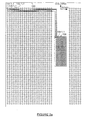
- FIG 10 is an isometric cross-sectional view of the programmable printed circuit board of this invention.
- programmable PC board 100 comprises a plurality of layers 101-1 through 101-4 of insulating material.
- On each layer 101-i (where 1 ⁇ i ⁇ 4) is formed a plurality of electrical traces 103.
- Formed in the printed circuit board are a multiplicity of component holes 102-1,1 through 102-R,C where R represents the number of component rows of holes formed on the programmable printed circuit board and C represents the number of columns of component holes formed on the board.
- the programmable printed circuit board illustrated in Figure la has rows of component holes 102-1,X through 102-R,X (where X is an integer which varies from 1 to C) and has columns of component holes 102-Y,1 through 102-Y,C where Y is an integer which varies from 1 to R.
- traces 103-1,1 through 103-1,C, 103-2,1 through 103-2,C and 103-3,1 through 103-3, C are formed on the top surface of insulating layer 101-1.
- Traces 103-4,1 through 103-6,C are formed on the top surface of layer 101-2.
- Traces 103-7,1, through 103-9,C are formed on the top surface of layer 101-3 and traces 103-10,1 through 103-12, C (not shown) are formed on the top surface of layer 101-4.
- Each trace 103-r,c (where r indicates the row and is given by 1 ⁇ r ⁇ R and c indicates the column and is given by 1 ⁇ c ⁇ C) interconnects a corresponding component hole 102-r,c to a corresponding PIC hole 104-r,c (shown in Figure lb) connectable to a selected pin on programmable interconnect chip 105 (shown in Figure 1a).
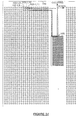
- Figure 1b illustrates PIC hole 104-r,c connected to trace 103-r,c so as to bring the electrical signal on trace 103-r,c to the top surface of layer 101-4 of the PC board 100 for electrical contact to the programmable interconnect chip (shown in Figure la but not in Figure 1b) of this invention.
- Figure lb shows an isometric cutaway drawing of a portion of the programmable printed circuit board 100 of this invention with PIC holes 104-1,1 through 104-R,C (not shown) being arranged in a selected location on the printed circuit board 100 so as to bring to a portion of the top surface of insulating layer 101-4 of the printed circuit board 100 the electrical signals carried by traces 103-1,1 through 103-R,C.
- the PIC holes 104-L,1 through 104-R,C are arranged in a pattern on the printed circuit board so as to mate with the pins or other electrical connections on the package containing the programmable interconnect chip.
- the area of the programmable PC board 100 occupied by PIC holes 104-1,1 through 104-R,C is desirably (though not necessarily) much smaller than the area of the printed circuit board occupied by component holes 102-1,1 through 102-R,C.
- the internal diameter of the PIC holes 104-1,1 to 104-R,C is much smaller than the internal diameter of the component holes 102-1,1 to 102-R,C and is only sufficient to allow the pins or other electrical connectors on the package of the programmable interconnect chip to make proper electrical contact to traces 103-1,1 through 103-R,C.
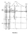
- Figure 2a illustrates in top view the local interconnect architecture of the programmable interconnect chip 105 mounted on the programmable printed circuit board 100 of this invention to show the conductive paths followed by the traces 103 interconnecting the component holes 102 to the PIC holes 104.
- Figure 2a illustrates the conductive traces on one layer 101-1 of PC board 100 only. Each layer of PC board 100 will have a similar pattern of traces.
- the regions under programmable interconnect chip 105 to which the traces are directed differ from level to level because each trace 103-r,c uniquely interconnects one component hole 102-r,c to a corresponding PIC hole 104-r,c.
- Figure 2b is similar to Figure 2a except it illustrates schematically the trace interconnect structure to interconnect component holes 102-r,c to PIC holes 104-r,c utilizing the traces 103-r,c on printed circuit board insulating layer 101-2. Note that the traces 103 on insulating layer 101-2 interconnect different component holes 102 and PIC holes 104 than do the traces shown in Figure 2a. Similar drawings for the interconnect traces formed on insulating layers 101-3 and 101-4 are shown in Figures 2c and 2d illustrating the different component holes 102-r,c being connected to the PIC holes 104-r,c by the traces 103-r,c on the layers of insulation 101-3 and 101-4.
- Figures 2a through 2d illustrate a programmable printed circuit board 100 utilizing one programmable interconnect chip 105 of this invention
- more than one programmable interconnect chip 105 can be used with a printed circuit board 105 if desired.
- the printed circuit board 100 must be configured to provide a plurality of PIC holes 104 beneath each of the programmable interconnect chips 105 utilized on the PC board 100. But with this change the structure of this invention can be made even more flexible and versatile than is possible with just one programmable interconnect chip 105.
- a plurality of programmable interconnect chips 301-1 through 301-7 are utilized on PPCB 300.
- programmable PC board 300 is a multilayer PC board although in certain simple configurations a single layer programmable PC board can be used.
- Each chip 301-j (where j is an integer represented by 1 ⁇ j ⁇ J) comprises a local programmable interconnect chip.
- a selected number of pins on chip 301-j are designated to electrically connect to the conductive traces in a bus formed on the programmable PC board 300 to interconnect that programmable interconnect chip 301-j to an adjacent programmable interconnect chip 301 such as chip 301-(j+1).
- programmable interconnect chip 301-1 is capable of interconnecting any one of a plurality of electronic components (not shown) mounted on PC board 300 adjacent to PIC 300-1 with another of that plurality of electronic components.
- programmable interconnect chip 301-1 is also able to connect these electronic components by means of buses 303-1 and/or 303-5 to the electronic components connected to adjacent programmable interconnect chips 301-2 and 301-5, respectively.
- busses 303-1 and 303-5 contain eight communication channels (i.e. eight traces) or 16 communication channels or data paths (i.e., 16 traces). Of course, these data busses can contain any number of transmission channels desired depending upon the requirements of the circuitry.
- the particular data busses 303-1 and 303-5 are formed by means of conductive traces formed on a selected surface of PC board 300.
- programmable interconnect chip 301-2 is connectable to programmable interconnect chip 301-3 and 303-4 by means of conductive busses 303-2 and 303-4, respectively.
- Conductive busses 303-2 and 303-4 have the same characteristics as conductive busses 303-1 and 303-5 previously described and thus will not be described in detail.
- conductive busses 303-3, 303-6, 303-7 and 303-8 interconnect selected programmable interconnect chips.
- conductive bus 303-3 interconnects programmable interconnect chip 301-3 to programmable interconnect chip 301-7.
- Conductive bus 303-7 interconnects programmable interconnect chip 301-4 to programmable interconnect chip 301-6.
- Conductive bus 303-6 interconnects programmable interconnect chip 301-5 to programmable interconnect chip 301-6 and conductive bus 303-8 interconnects programmable interconnect chip 301-6 to programmable interconnect chip 301-7.
- Conductive busses 303-3 and 303-6 through 303-8 each have the same characteristics as described above in conjunction with conductive busses 303-1 and 303-5 and thus this description will not be repeated.
- the structure of Figure 3a allows any electronic component on the PPCB to be interconnected with any other electronic component on the PPCB through one or more PIC's.
- Figure 3b illustrates a second type of interconnect system wherein programmable interconnect chips 311-1, 311-2, 311-3, and 311-4 are interconnected by means of conductive busses 313-1 through 313-6.
- each programmable interconnect chip 311-1 through 311-4 shown in Figure 3b is connected directly to an adjacent programmable interconnect chip 311 by means of a dedicated conductive bus 313.
- programmable interconnect chip 311-1 can be connected directly to programmable interconnect chips 311-2, 311-3 or 311-4 by means of conductive busses 313-1, 313-5 or 313-4, respectively.
- Each of these conductive busses contains a selected number of conductive lines (such as 8 or 16 conductive lines) implemented by means of 8 or 16 traces formed on a particular surface of programmable PC board 300.
- conductive busses 313-6, 313-2 and 313-3 have 8 or 16 conductive paths represented by traces formed on the PC board 300 and interconnect pairs of the programmable interconnect chips as shown in Figure 3b.
- the advantage of the structure shown in Figure 3b over the structure shown in Figure 3a is that each programmable interconnect chip 311 is able to communicate directly to each of the other programmable interconnect chips 311 on the printed circuit board 300.
- each programmable interconnect chip 311 also interconnects a plurality of electrical components such as integrated circuits or discrete devices inserted into the programmable PC board in the area adjacent to the programmable interconnect chip 311.
- programmable interconnect chip 311-1 interconnects electronic components (not shown) formed in the upper left quadrant 300-1 of programmable PC board 300.
- Programmable interconnect chip 311-2 interconnects electronic components (not shown) inserted into the programmable PC board 300 in upper right quadrant 300-2.
- Programmable interconnect chip 311-3 interconnects electronic components (not shown) inserted into the programmable PC board 300 in the lower right quadrant 300-3 and programmable interconnect chip 311-4 interconnects electronic components (not shown) inserted into the lower left quadrant 300-4 of programmable PC board 300.
- the structure of Figure 3b is capable of electrically interconnecting the electronic components within each quadrant not only among themselves but also to the electronic components in other quadrants of the programmable PC board 300.
- the structure of Figure 3b thus gives great flexibility to the circuit designer in locating the electrical components to perform a given system function.
- Figure 3c illustrates a bus configuration wherein a central bus 323-10 is formed on PC board 300 and programmable interconnect chips 321-1, 321-2, 321-3, 321-4, 321-5 and 321-6 are connected by means of conductive busses 323-1, 323-2, 323-3, 323-4, 323-5 and 323-6, respectively, to central conductive bus 323-10.
- Central bus 323-10 is formed by placing conductive traces on printed circuit board 300.
- Conductive busses 323-1 through 323-6 are similarly formed by placing conductive traces on the PC board.
- PC board 300 in general is a multilayer PC board with two or more layers of conductive traces.
- the structure shown in Figure 3c requires the traces making up bus 323-10 to be formed on one layer of PC board 300 and the traces comprising conductive busses 323-1 through 323-6 to be formed on a second layer. Electrical contact is then made between selected ones of the traces comprising busses 323-1 through 323-6 to the traces comprising bus 323-10 by means of holes, each hole electrically contacting the two or more traces to be interconnected.
- Figure 3c simplifies the interconnections of the programmable interconnect chips 321-1 through 321-6 and improves the speed of interconnection of the common global bus signals but requires the establishment of a protocol for use of bus 323-10.
- Bus protocol is handled in a manner well known in the art by the programmable interconnect chips 321-1 through 321-6.
- FIG. 3d An additional interconnect structure is shown in Figure 3d.
- programmable interconnect chips 331-1, 331-2, 331-3, 331-4, 331-5, 331-6 and 331-7 are interconnected by means of busses 333-1, 333-2, 333-3, 333-5, 333-6 and 333-7 all of which emanate from or go to central programmable interconnect chip 331-4.
- Chip 331-4 is primarily or exclusively dedicated to interconnecting the programmable interconnect chips 331-1 through 331-3 and 331-5 through 331-7. If desired and if the pins are available on programmable interconnect chip 331-4, programmable interconnect chip 331-4 also interconnects electronic components mounted on the programmable PC board particularly in the regions electrically adjacent to programmable interconnect chip 331-4.
- Each of the programmable interconnect chips 331-1 through 331-3 and 331-5 through 331-7 interconnects electronic components mounted on the PC board in areas adjacent to the programmable interconnect chip and has a certain number of pins (depending upon the number of conductive paths in each of busses 333-1 through 333-3 and 333-5 through 333-7) dedicated to interconnecting itself, through PIC 331-4, to other programmable interconnect chips 331.
- the advantage of the structure in Figure 3d is that programmable interconnect chip 331-4 can be configured to control the protocol for communication between each of the other programmable interconnect chips 331-1 to 331-3 and 331-5 to 331-7 and to improve the speed of the random global interconnections between the non adjacent programmable interconnect chips.
- Figure 4a illustrates a programmable printed circuit board 400 of this invention containing a number of different structures for both physically and electrically connecting the electronic components to the programmable PC board 400.
- an electronic component is capable of being inserted into sockets in the PC board such that leads on the component's package electrically connect to and are physically retained by electrically conductive component holes (such as component hole 402-1,1) in the PC board.
- the holes are shown formed on a standard grid pattern such that one type of programmable PC board can be used regardless of the circuit function to be performed.
- This type of component hole called a socketed PCB configuration, allows the electrically conductive pins on component packages to be inserted into the component holes 402 in the PC board 400 and also to be removed from these component holes 402 (such as hole 402-1,1) without destroying the package pins.
- the lower left portion of PC board 400 has been configured to contain electronic component packages which are soldered into the programmable PC board 400.
- component holes such as hole 402-R,1 are also used in this configuration and the holes can be placed in the board in accordance with the pin configuration of the electronic component packages to be mounted in the board.
- row R-1 one row of holes (row R-1) is shown omitted from the PC board in the lower left hand corner.
- the disadvantage of soldering components to the PC board is that the components cannot be easily removed.
- the advantage is greater structural integrity, lower cost and higher reliability. Soldered PC boards are commonly used in production to ensure high reliability and quality and lower cost in the resulting product.
- the lower right hand corner of the PC board 400 in Figure 4a comprises a solder pad configuration for the mounting of electronic components on the programmable PC board.
- each pad such as pad 402P-R,C
- the solder pads can be formed on programmable PC board 400 in accordance with the connection configuration of the components to be mounted on the board, such as surface mounted devices.
- Figure 4b shows an end view of the structure shown in top view in Figure 4a.
- the socketed PC board can use an adaptive socket 407 of a type commonly known in. the industry.
- appropriate sockets are produced by Augat Interconnection Systems of 40 Perry Avenue, Attleboro, Massachusetts 02703 and are disclosed in Chapter 7 of revision 5.0 of their July 1987 Engineering Design Guide.
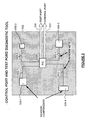
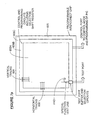
- Figure 5 illustrates a single programmable interconnect chip 505 placed on the center of programmable PC board 500.
- Electronic components 506-1 through 506-4 are mounted at various places on the programmable PC board 500 and are interconnected by conductive traces, shown schematically as 503-1, 503-2, 503-3 and 503-4, to programmable interconnect chip 505.
- Programmable interconnect chip 505, however, has two busses extending from it to ports on the edge of the printed circuit board.
- These ports comprise a test port 508 for the transmission of test signals from an external source such as a computer to programmable interconnect chip 505 to test the state of each conductive trace 503 coming into programmable interconnect chip 505 and a control port 509 for allowing control signals from an external source such as a computer to be transmitted to programmable interconnect chip 505 to control the configuration of programmable interconnect chip 505.
- the two ports 508 and 509 can be actuated simultaneously such that the computer can determine that the proper signals are present on selected traces connected to PIC 505 during the configuring of PIC 505 and during the operation of the system represented by FPPCB 500 and the attached electronic components 506-1 through 506-4 and PIC 505.
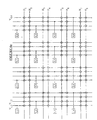
- FIGS 6a and 6b illustrate a programmable interconnect chip 605 in accordance with this invention suitable for implementing the programmable interconnect function in the structures described above.
- the programmable interconnect chip 605 contains a plurality of cells 606-1,1 through 606-S,T where S represents the number of rows of cells in the programmable interconnect chip 605 and T represents the number of columns of cells in chip 605.
- Each cell has an array of electrically conductive pads 607-1,1 through 607-M,N where M represents the number of rows of pads in the cell and N represents the number of columns of pads in the cell.
- each cell is identical in configuration, only the conductive pads 607 associated with cell 606-1,1 will be described in detail with the understanding that the conductive pads associated with each of the other cells 606-s,t (where s is an integer given by 1 ⁇ s ⁇ S and t is an integer given by 1 ⁇ t ⁇ T) in chip 605 function identically.
- Figure 6b illustrates the configuration of cell 606-1,1 and also of each of the other cells 606-s,t.
- horizontal conductive tracks 608-1 through 608-J (where J is an integer representing the maximum number of horizontal conductive tracks formed on programmable interconnect chip 605) are shown.
- vertical conductive tracks 609-1 through 609-K are shown where K is an integer representing the maximum number of columns of conductive tracks formed on programmable interconnect chip 605.
- the horizontal conductive tracks 608-1 through 608-J are formed on one level of interconnections on chip 605 while the vertical conductive tracks 609-1 through 609-K are formed on a second level of interconnections on chip 605.
- the horizontal conductive leads 608-1 through 608-J have differing lengths across the chip.
- the cell 606-1,1 shown in the upper left hand corner of both Figure 6a and Figure 6b has a plurality of horizontal conductive leads 608 originating in and extending from cell 606-1,1 to each of the other cells 606-1,2 through 606-1,T in the same row.
- cell 606-1,1 has a plurality of vertical conductive leads 609 extending from cell 606-1,1 to each of the other cells 606-2,1 to 606-S,1 in the same vertical column.
- the horizontal and vertical traces 608 and 609 have at each of their intersections a programmable connective structure such as for example, an antifuse.
- an antifuse comprises a capacitive structure with a dielectric capable of being broken down by the application of a selected voltage to provide a conductive path between the two plates of the capacitor.
- Antifuses are well known in the art and thus will not be described in detail. Other kinds of programmable elements can also be used depending upon design considerations.
- the substrate of the programmable interconnect chip 605 has formed in it selected transistors to enable the programming of the antifuse elements at selected intersections in accordance with design requirements.
- vertical leads 609-1 through 609-K are formed on the programmable interconnect chip 605 so as to extend at a minimum across one cell 606 and at a maximum across all cells.
- a plurality of vertical leads 609 cross each cell with the lengths of leads varying from being such as to extend across just that cell to being such as to extend across all cells in a column.
- Horizontal conductive leads 608-1 through 608-J likewise extend across the programmable interconnect chip 605. Again, the horizontal leads 608 extending across one cell vary in length such that they extend across only that one cell up to a length which will extend across all cells.
- breaklines are included to indicate that the semiconductor chip 605 is only partially shown with interior portions of the chip having been removed for clarity. However, some conductive leads break not because of the breaklines showing removal of semiconductor material but rather because the conductive leads are intended to stop at a given point. Small lines 618-1, 618-2 and 618-3 are drawn at the terminal points of a conductive lead perpendicular to that lead to indicate that the conductive lead is intended to terminate at those points.
- a horizontal conductive lead thus might comprise one conductive segment extending across the whole chip 605 or a plurality of conductive segments each extending across a section of the chip.
- the vertical conductive leads likewise vary from one conductive lead which will extend across the entire height of the chip or two or more conductive segments each extending across a selected portion of the chip.
- the particular configuration of the conductive leads extending across one cell and from that cell to adjacent cells depends upon an analysis of the electrical functions to be carried out by the programmable printed circuit board and is selected using the most probable types of system requirements to be imposed on programmable interconnect chip 605. This selection depends upon an analysis of the circuit functions to be performed by the programmable printed circuit board of this invention and thus the actual configuration of the programmable interconnect chip is determined in light of the proposed uses for the programmable printed circuit board.
- an interconnection between the appropriate vertical conductor 609 and the appropriate horizontal conductor 608 is formed.
- the intersection of vertical lead 609-1 and horizontal lead 608-1 is programmed by applying a high voltage to this intersection in the circuit so as to break down the dielectric between these two points and form a conductive path therebetween.
- Figure 6b also illustrates the particular connections which must be formed to connect pad A to pad D, pad A to pad C or pad A to pad E. Should all of these connections be made then pads B, D, C and E will also be connected to each other through pad A.
- Figure 6c illustrates a programmable interconnect chip 605 utilizing a single cross-point switch matrix array.
- the structure of Figure 6c has certain advantages of simplicity and ease of fabrication.
- the structure shown in Figure 6c is simpler than that shown in Figure 6b in that each pad (such as pad A) is connected by a conductive trace (such as conductive lead 625-A) permanently to a vertical conductive lead (such as lead 629-1.
- the vertical conductive lead 629-1 is permanently connected by via 624-1 (as shown by the solid dot) to horizontal conductive line 628-1.
- the circuit is programmed by applying a voltage at the correct node (such as node 623-1) to form a conductive path between desired vertical and the horizontal leads (such as horizontal lead 628-1 and vertical lead 629-4) thereby to connect pad A to pad B.
- Pad B is connected to vertical lead 629-4 by conductive trace 625-B.
- each vertical line is permanently connected to one horizontal line 628 by a via (such as via 624-1). This greatly simplifies the interconnection required to program the printed circuit board of this invention since one pad can be connected to another by only one programming element.
- this particular structure becomes relatively inefficient in its use of space on the programmable interconnect chip 605.
- the total number of programming elements required equals the number of pads squared.
- Figure 6d shows a variation of the structure in Figure 6c.
- interconnect pad A which connects to a PIC hole such as hole 104-1,1 shown in Figure 1b
- pad D which connects to a similar PIC hole 1004.
- two programming elements must be programmed.
- the element at the intersection of vertical lead 639-1 and horizontal lead 638-1 must be programmed as must the element at the intersection of vertical lead 639-(K-1) and horizontal lead 638-1.
- each conductive pad such as pad A or pad D is connected by means of a conductive trace such as trace 635-A to a vertical lead 639.
- the number of horizontal leads is in this embodiment less than 1/2 the number of vertical leads because each horizontal lead connects two pads whereas each vertical lead is connected directly to one pad only.
- the structure of Figure 6d has greater flexibility than that shown in Figure 6c at the price of two programming elements per connection rather than one.
- the number of programming elements is 1/2 the square of the number of pads. As the number of pads become larger (for example above 200 to 500 pads) this structure becomes relatively inefficient.
- Figure 6e illustrates the single switch cross-point matrix array of Figure 6c with interconnections formed to connect pad 1,1 to pad 4,1.
- the intersection of the vertical lead V 1,1 and the horizontal lead H 1 is programmed as is the intersection of the vertical lead V 4,1 and horizontal lead H 1 .
- two elements have been programmed to connect pads 1,1 and 4,1.
- the programming elements at the intersection of the vertical lead V 1,2 , and the horizontal lead H 3 and of the horizontal lead H 3 and the vertical lead V 4,4 are programmed.
- Figure 7a shows in block diagram form the architecture of the programmable interconnect chip 605.
- the interior 605A of chip 605 contains the cells 606 (as described in conjunction with Figures 6a through 6e) and the horizontal and vertical tracks 608 and 609 respectively.
- peripheral area 605B which forms an annular square around interior 605A are placed control and programming circuits including shift registers for selecting particular horizontal and vertical tracks the intersections of which are to be programmed.
- buffer circuitry for the test port bus and the control port bus is provided in this region of chip 605.
- Annular region 605C surrounds annular region 605B and contains additional circuitry essential to the operation of the chip such as mode selection circuitry which will determine whether the programmable interconnect chip is in the test mode, the operating mode or the programming mode. Additional special circuitry as required will also be placed in peripheral region 605C.
- Figure 7b illustrates a programming structure and particularly programming transistors and circuits to select the intersection to be programmed of horizontal and vertical conductive leads on the programmable interconnect chip using only two transistors in the programming circuit path. Utilization of the structure shown in Figure 7b allows the programming current to reach into the hundreds of milliamps to amperes range necessary to break down the dielectric between the vertical and horizontal conductive leads to form an interconnection therebetween with sufficiently low resistance.
- transistors Q1 and Q2 are provided to program the intersection of vertical conductive track V 1 and horizontal conductive track H 1 .
- Transistor Q1 has its gate connected to voltage source VGP 1 and transistor Q2 has its gate connected to a voltage source HGP 1 .
- the source of transistor Q1 is connected to vertical conductive track V1 while the drain of transistor Q1 is connected to conductive lead VDP 1 .
- the source of transistor Q2 is connected to horizontal lead H 1 and the drain of transistor Q2 is connected to conductive lead HDP 1 .
- VGP 1 is applied to take the gate of Q1 to a high voltage V GH , the gates of other transistors in the array such as transistor Q3 are held at zero volts and the drain voltage VDP1 on transistor Q1 is taken to V PP .
- the gate voltage of Q4 is taken high because HGP 1 is taken to a high voltage to turn on transistor Q2.
- the voltage on the drain of Q2 is taken to zero volts by driving HDP 1 to zero and HDP 2 which applies a voltage to the drain of Q4 is taken to zero or to v PP /2 (which voltage is selected so as not to program the programming element at the intersection of V 2 and H 2 .
- V PP the programming voltage
- V GH which is applied to lead VGP 1
- V PP is larger than V PP by the transistor threshold voltage and thus is approximately 18 to 53 volts.
- the threshold voltage of these transistors is made approximately 3 volts.
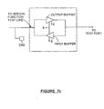
- Figure 7c shows a bidirectional amplifying circuit capable of amplifying signals coming in either direction depending upon control signals applied to the input and output buffers contained within the circuitry.
- each pad on PIC 605 is connected to a special function test line (illustrated in Figure 7c) and the special function test line is then capable of being connected to the test port by turning on the output buffer through a high level signal applied to the lead labeled S on the output buffer together with a high level enable signal applied on the terminal labeled E.
- a low level signal is applied to the lead labeled S to the input buffer thereby turning off the input buffer.
- Reverse polarity signals applied to terminals S and S result in the input buffer turning on and the output buffer turning off thereby allowing a signal from the test port to be applied to the pad.
- the S and E signals are transferred to the peripheral circuits in annular region 605B of Figure 7a to select the pads on the PIC and the leads of the components on the FPPCB to connect to the test port.
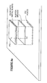
- Figures 8a and 8b illustrate structures for attaching the program interconnect chip such as chip 105 in Figure la to the PC board 100.
- Figure 8a illustrates a program interconnect chip which contains pads with metal bumps shown in an exploded view above the PIC holes (corresponding to holes 104-1,1 through 104-R,C shown in Figure 1b).
- a buffer medium comprising an elastomeric material which under pressure will conduct in the vertical direction but not the horizontal direction, is shown placed between the program interconnect chip and the PIC holes.
- the buffer medium could also be a carrier using button springs of a type well known in the art. This medium is a good buffer between the surface of the PIC and FPPCB with their different surface flatness and temperature coefficient.
- the particular structure to be used to attach the programmable interconnect chip to the programmable PC board will depend upon the design requirements for the particular system utilizing the combination of programmable PC board and programmable interconnect chip and cost considerations.
- Figure 8b which consists of Figure 8b1 and 8b2, shows an alternative structure for attaching the programmable interconnect chip such as chip 105 in Figure 1a directly to a programmable printed circuit board such as board 100 in Figure 1a.
- the programmable interconnect chip has formed on one surface thereof a conductive pad to serve as an interface between a conductive element on the chip and a metal bump consisting of a soft solder such as lead tin placed on a nickel bottom layer.
- the whole bump is made of indium.
- the nickel is used to give strength to the bump.
- the programmable PC board has solder formed in the PIC hole so as to form a bump on the surface of the PC board to which the programmable interconnect chip is to be attached.
- the PIC hole such as hole 104-r,c in Figure 1b is plated typically with copper to a selected thickness such as 1 mil.
- the solder bump will, when the programmable interconnect chip is brought into pressure contact with the solder and the combined structure heated, form a solid contact with the metal bump. The two materials will wet and become one thus firmly securing and electrically connecting the programmable interconnect chip to the programmable printed circuit board. Solder bumps are well known in the art and thus this structure will not be described in greater detail.
- Other structures can be used to attach the programmable interconnect chip such as chip 105 in Figure la directly to a programmable printed circuit board such as board 100 in Figure la. Such structures include attachment of the PIC on the board and wire bonding of the pads on the PIC to the PIC holes. Any other structure known in the art to attach electronic components to a printed circuit board can be used with this invention and the structures described for this purpose are exemplary only.
- a printed circuit board comprises a first portion containing conductive traces for interconnecting electronic components formed thereon without the use of a programmable integrated circuit and a second portion containing at least one programmable integrated circuit for interconnecting electronic components formed on at least the second portion of the printed circuit board.
- Electronic components formed on the second portion of the printed circuit board are in some cases interconnected with the electronic circuit formed on the first portion of the printed circuit board by conductive traces.
- These conductive traces typically will run from the first portion of the printed circuit board to at least one programmable integrated circuit for interconnecting electronic components formed on the second portion of the printed circuit board, thereby to electrically connect the second portion of the printed circuit board to the first portion of the printed circuit board.
Abstract
Description
- This application is a divisional application of EP 90 310 252.3.
- This invention relates to printed circuit boards and in particular to a printed circuit board which is programmable in the field by the designer of an electronic system to provide a desired function. The invention also relates to a method of configuring an electronic system formed with a programmable printed circuit board.
- Printed circuit boards are commonly used in electronic devices such as instruments, computers, telecommunication equipment and consumer electronic products. Typically, an engineer will design a printed circuit board to carry the types of components necessary to implement the desired electronic function and to fit in the space available for the board. Consequently, each printed circuit board typically is custom designed. To design a custom printed circuit board is expensive, takes time and requires the fabrication of prototype printed circuit boards. If errors are found in the prototypes, then the printed circuit board must be redesigned. Such a process often delays the planned introduction of a new product.
- U.S. Patent 4,779,340 discloses a prior approach to overcoming the above problems whereby a carrier board contains contacts for receipt of electronic components and electrically conductive traces formed on the board, each component contact being connected via a corresponding trace to contacts along one edge of the board. An interconnection board in user-configured to provide the required interconnections between components when the interconnection board is connected to the carrier board edge contacts by cable and/or connectors.
- Japanese Patent Publication 59-161839 disclosed mounting logic chips, such as PLA chips, on a substrate/ wiring array chips are also mounted on the substrate and are connected to the logic chips through a single layer of wiring patterns. The logic chips are interconnected in a desired manner by appropriately programming the wiring array chips.
- According to the present invention, there is provided a structure as defined in
claim 1. - In accordance with this invention, a printed circuit board of unique configuration may be combined with one or more special programmable integrated circuit chips (hereinafter called "programmable interconnect chips" or "PICs") to provide a user programmable printed circuit board capable of being used to provide any one of a plurality of functions.
- In one embodiment of the invention, a field programmable printed circuit board comprises
- (1) a multiplicity of component contacts for receipt of the leads of electronic components;
- (2) a corresponding multiplicity of PIC contacts for receipt of the leads on the package or packages of the programmable interconnect chip or chips; and
- (3) multiple layers of conductive traces, each conductive trace uniquely connecting one component contact to one PIC contact.
-
- Typically, electronic components comprise integrated circuits and/or discrete devices contained, respectively, in standard integrated circuit or discrete device packages and in addition, discrete elements which include resistors, capacitors and inductors, for example.
- Generally the component contacts and PIC contacts comprise holes in the printed circuit board, the interior surfaces of which are plated to a selected thickness with a conductive material such as copper. Alternatively, these contacts are pads or any other structure for electrically and physically joining electronic components and integrated circuits to a printed circuit board. Advantageously, the PIC contacts are usually (though not necessarily) smaller than the component contacts so that the area of the programmable printed circuit board occupied by the programmable interconnect chip or chips is much smaller than the area of the printed circuit board occupied by the electronic components. Each PIC contact brings a corresponding trace from a selected level on the PC board to the surface of the PC board so that trace is then connectable to a pin or electrical contact on a programmable interconnect chip. For every component contact (the function of which is to receive the pin or electrical contact of an electronic component) there is a corresponding electrically conductive trace which interconnects that component contact to a corresponding PIC contact (the function of which is to receive the pin or electrical contact of the programmable interconnect chip) in the printed circuit board. Thus, each component contact is electrically and uniquely connected to a corresponding PIC contact for electrically contacting a programmable interconnect chip of this invention.
- In accordance with this invention more than one programmable interconnect chip may be, if desired, placed on a printed circuit board to provide enhanced interconnection flexibility and cost optimization for the electronic components on the printed circuit board. Such a board then has additional PIC contacts corresponding to and for connection to the external pins or electrical contacts on the additional packages containing the additional programmable interconnect chips.
- The field programmable printed circuit board (hereinafter sometimes referred to as an "FPPCB") of this invention substantially reduces the cost associated with developing complex electronic systems by providing a standard PC board configuration which is easily and economically manufactured. In accordance with this invention, the designer of electronic systems utilizing the standard programmable PC board of this invention will also utilize computer aided design software to determine the optimum placement of the electronic components on the programmable PC board and to determine the configuration of the programmable interconnect chip or chips of this invention to properly interconnect the electronic components so as to yield the desired electronic system.
- In accordance with the method of this invention a user designing an electronic system utilizing the programmable PC board of this invention may first enter a model of the programmable PC board into the computer aided design system. The model includes (A) component contacts for receiving the electrical leads of electronic components, (B) PIC contacts for receiving the electrical leads of one or more programmable interconnect chips, and (C) conductive traces for connecting the component contacts to the PIC contacts.
- The user then may enter the placement of the desired electronic components, be they discrete elements, memory, logic gates, or microprocessors, on selected component contacts on the programmable PC board and will enter (A) the interconnection of these electronic components using (B) the configuration of the PIC(s) used for the interconnection using the standard PC board of this invention together with the programmable interconnect chip or chips of this invention. The computer will then simulate the electrical performance of the system with the electrical components so placed and interconnected and will indicate the resulting electrical performance so as to indicate whether or not the configuration selected by the designer yields the desired electronic function. The user may then either modify the placement of the components or modify the PIC interconnection configuration, and repeat the simulation step as appropriate.
- The designer will have choices in the placement of the electronic components on the programmable PC board and in their interconnection but will be assisted in this placement by certain logical rules contained in the computer aided design program. Algorithms for use in computer aided design systems of the type required to implement the design of electronic systems utilizing the programmable PC board and programmable interconnect chip of this invention are of a type currently available in the electronic design industry.
- Examples of algorithms suitable for partitioning and placement of the electronic components on the programmable PC board of this invention are described in (a) Lauther, "A Min-Cut Placement Algorithm for General Cell Assemblies Based on a Graph Representation," 16th Design Automation Conf., June 25-27, 1979, pp. 1 - 10, reprinted in Comp. Paps. Design Automation Conf., 1988, pp 182-191, and (b) Fiduccia et al, "A Linear-Time Heuristic for Improving Network Partitions," 19th ACM/IEEE Design Automation Conf., June 14 - 16, 1982, p. 175 - 181 reprinted in ibid., pp. 241 - 247. Examples of algorithms suitable for routing of the programmable interconnect chip(s) are described in (c) Marek-Sadowska, "Two Dimensional Router for Double Layer Layout," 22nd ACM/IEEE Design Automation Conf., June 23 - 26, 1985, pp. 117 - 123, (d) Tzeng et al, "Codar: A Congestion-Directed General Area Router," IEEE Int'l Conf. on CAD, Nov. 7 - 10, 1988, pp. 30 - 33, (e) Lin et al, "A Detailed Router Based on Simulated Evolution," ibid., pp. 38 - 41, and (f) Lee et al, "A New Global Router for Row-Based Layout," ibid., pp. 180-183.
- The programmable printed circuit board of this invention is considered to be "field programmable" because the designer of an electronic system is able to program the placement of electronic components on the unique PC board of this invention by using and configuring the programmable interconnect chips of this invention. The PC board of this invention is unique in that it has a standard configuration regardless of the electronic function to be implemented and thus is relatively inexpensive and easy to make. At the same time, the field programmable PC board of this invention is programmable by use of one or more programmable interconnect chips.
- In an alternative embodiment of this invention, the programmable PC board of this invention includes on a portion of its surface electronic components which are interconnected using custom designed interconnections to form a particular circuit function. Conductive traces transmit the signals from this custom portion of the PC board to one or more programmable interconnect chips on the remainder of the PC board. The programmable interconnect chip or chips are configured by the user to achieve the desired function required utilizing both the custom portion of the PC board and the programmable portion of the PC board.
- Throughout this specification, the field programmable PC board of this invention will usually be described as having component holes and PIC holes for receipt of the electrical leads of the electronic components and of the programmable interconnect chip, respectively. The term "component hole" and the term "PIC hole" will be used to describe a standard hole formed in a PC board and plated with a conductive material as in the prior art to receive a conductive lead. However, any conductive structure capable of being used to electrically contact and physically hold the package of an electronic component can be used in place of a component hole or a PIC hole. Such a structure includes a solder pad and a socketed printed circuit board opening for.slidably receiving and releasing the pins of an electronic component package. It should be noted that the term PIC hole is used to distinguish the function of certain holes in the programmable printed circuit board of this invention from the component holes. However, both types of holes are plated with a conductive material and have the same purpose -- that is to electrically transmit signals from either the pin of the package of an electronic component to a conductive trace or from a conductive trace to the pin of an electronic component or through the programmable interconnect chip to another trace or from a conductive trace to another conductive trace.
- In certain circumstances, a PIC hole or a component hole can be used to interconnect two traces directly. Such a configuration occurs in custom designed PC boards.
- This invention will be more fully understood in conjunction with the following detailed description together with the attached drawings, in which:
- Figure 1a illustrates in isometric view a programmable printed circuit board of this invention containing a plurality of layers of traces such as trace 103-r,c each trace connecting uniquely one component hole 102-r,c to a corresponding PIC hole 104-r,c (shown in Figure 1b);
- Figure 1b illustrates an isometric view of the
portion of the
programmable PC board 100 of Figure la beneathprogrammable interconnect chip 105 containing the PIC holes (such as hole 104-r,c) for connection of the traces (such as trace 103-r,c) to the pins or electrical contacts on theprogrammable interconnect chip 105 of this invention; - Figures 2a through 2d illustrate schematically
four top plan views of printed
circuit board 100 utilizing theprogrammable interconnect chip 105 of this invention together with the multiplicity of component holes 102-1,1 through 102-R,C (not shown) arranged on the printed circuit board together with a schematic representation ofconductive busses 103 each bus containing a plurality of conductive traces such as traces 103-1,1 through 103-1,3 for interconnecting each of thecomponent holes 102 to acorresponding PIC hole 104 beneath theprogrammable interconnect chip 105; - Figures 3a, 3b, 3c and 3d illustrate a number of different global interconnect architectures suitable for use with this invention;
- Figures 4a, 4b and 4c illustrate a
programmable printed
circuit board 400 constructed in accordance with this invention together with aprogrammable interconnect chip 405 placed on the board to interconnect the electronic components to be placed on thePC board 400 in a selected manner to provide the desired electronic function; - Figure 5 illustrates a programmable
printed circuit board 500 of this invention containing a test port and a control port for testing the state of each trace on the programmable printedcircuit board 500 and for configuring theprogrammable interconnect chip 505 to interconnect in the desired manner the electronic components 506-1 through 506-4 placed on thePC board 500; - Figures 6a through 6e illustrate a number of
structures for implementing the
programmable interconnect chip 605 suitable for use in implementing the programmable PC board of this invention; - Figure 7a illustrates the architecture of the
programmable interconnect chip 605; - Figure 7b illustrates one structure for
programming the intersection of two conductive leads
formed on the
programmable interconnect chip 605; - Figure 7c illustrates a bilateral circuit for
controlling the transmittal of signals to or from a test
port used in conjunction with the
programmable interconnect chip 605 of this invention; and - Figures 8a and 8b illustrate structures for connecting electronic component packages and/or a package containing a programmable interconnect chip to the programmable printed circuit board of this invention;
- Figure 8b consists of Figures 8b1 and 8b2.
-
- The following description is meant to be illustrative only and not limiting. Other embodiments of this invention will be obvious to those skilled in the art in view of this description.
- Figure 10 is an isometric cross-sectional view of the programmable printed circuit board of this invention. As shown in Figure 10,
programmable PC board 100 comprises a plurality of layers 101-1 through 101-4 of insulating material. On each layer 101-i (where 1 ≤ i ≤ 4) is formed a plurality ofelectrical traces 103. Formed in the printed circuit board are a multiplicity of component holes 102-1,1 through 102-R,C where R represents the number of component rows of holes formed on the programmable printed circuit board and C represents the number of columns of component holes formed on the board. Thus, the programmable printed circuit board illustrated in Figure la has rows of component holes 102-1,X through 102-R,X (where X is an integer which varies from 1 to C) and has columns of component holes 102-Y,1 through 102-Y,C where Y is an integer which varies from 1 to R. As shown in Figure la, traces 103-1,1 through 103-1,C, 103-2,1 through 103-2,C and 103-3,1 through 103-3, C (not shown) are formed on the top surface of insulating layer 101-1. Traces 103-4,1 through 103-6,C (not shown) are formed on the top surface of layer 101-2. Traces 103-7,1, through 103-9,C (not shown) are formed on the top surface of layer 101-3 and traces 103-10,1 through 103-12, C (not shown) are formed on the top surface of layer 101-4. Each trace 103-r,c (where r indicates the row and is given by 1 ≤ r ≤ R and c indicates the column and is given by 1 ≤ c ≤ C) interconnects a corresponding component hole 102-r,c to a corresponding PIC hole 104-r,c (shown in Figure lb) connectable to a selected pin on programmable interconnect chip 105 (shown in Figure 1a). - In the description of Figure la, for simplicity not all component holes 102-r,c are actually numbered nor are all traces 103-r,c numbered. However, the numbering of the component holes 102-r,c, traces 103-r,c and the PIC holes 104-r,c is consistent with each electrically connected component hole 102-r,c, trace 103-r,c and PIC hole 104-r,c all having the same indicia r,c.
- Figure 1b illustrates PIC hole 104-r,c connected to trace 103-r,c so as to bring the electrical signal on trace 103-r,c to the top surface of layer 101-4 of the
PC board 100 for electrical contact to the programmable interconnect chip (shown in Figure la but not in Figure 1b) of this invention. Figure lb shows an isometric cutaway drawing of a portion of the programmable printedcircuit board 100 of this invention with PIC holes 104-1,1 through 104-R,C (not shown) being arranged in a selected location on the printedcircuit board 100 so as to bring to a portion of the top surface of insulating layer 101-4 of the printedcircuit board 100 the electrical signals carried by traces 103-1,1 through 103-R,C. The PIC holes 104-L,1 through 104-R,C (each of which is plated on its interior surface with a conductive material) are arranged in a pattern on the printed circuit board so as to mate with the pins or other electrical connections on the package containing the programmable interconnect chip. Thus the area of theprogrammable PC board 100 occupied by PIC holes 104-1,1 through 104-R,C is desirably (though not necessarily) much smaller than the area of the printed circuit board occupied by component holes 102-1,1 through 102-R,C. The internal diameter of the PIC holes 104-1,1 to 104-R,C is much smaller than the internal diameter of the component holes 102-1,1 to 102-R,C and is only sufficient to allow the pins or other electrical connectors on the package of the programmable interconnect chip to make proper electrical contact to traces 103-1,1 through 103-R,C. - Figure 2a illustrates in top view the local interconnect architecture of the
programmable interconnect chip 105 mounted on the programmable printedcircuit board 100 of this invention to show the conductive paths followed by thetraces 103 interconnecting the component holes 102 to the PIC holes 104. Figure 2a illustrates the conductive traces on one layer 101-1 ofPC board 100 only. Each layer ofPC board 100 will have a similar pattern of traces. The regions underprogrammable interconnect chip 105 to which the traces are directed differ from level to level because each trace 103-r,c uniquely interconnects one component hole 102-r,c to a corresponding PIC hole 104-r,c. Figure 2b is similar to Figure 2a except it illustrates schematically the trace interconnect structure to interconnect component holes 102-r,c to PIC holes 104-r,c utilizing the traces 103-r,c on printed circuit board insulating layer 101-2. Note that thetraces 103 on insulating layer 101-2 interconnectdifferent component holes 102 andPIC holes 104 than do the traces shown in Figure 2a. Similar drawings for the interconnect traces formed on insulating layers 101-3 and 101-4 are shown in Figures 2c and 2d illustrating the different component holes 102-r,c being connected to the PIC holes 104-r,c by the traces 103-r,c on the layers of insulation 101-3 and 101-4. - While Figures 2a through 2d illustrate a programmable printed
circuit board 100 utilizing oneprogrammable interconnect chip 105 of this invention, more than oneprogrammable interconnect chip 105 can be used with a printedcircuit board 105 if desired. The printedcircuit board 100 must be configured to provide a plurality ofPIC holes 104 beneath each of theprogrammable interconnect chips 105 utilized on thePC board 100. But with this change the structure of this invention can be made even more flexible and versatile than is possible with just oneprogrammable interconnect chip 105. - As shown in Figure 3a a plurality of programmable interconnect chips 301-1 through 301-7 are utilized on
PPCB 300. Typically,programmable PC board 300 is a multilayer PC board although in certain simple configurations a single layer programmable PC board can be used. Each chip 301-j (where j is an integer represented by 1 ≤ j ≤ J) comprises a local programmable interconnect chip. A selected number of pins on chip 301-j are designated to electrically connect to the conductive traces in a bus formed on theprogrammable PC board 300 to interconnect that programmable interconnect chip 301-j to an adjacentprogrammable interconnect chip 301 such as chip 301-(j+1). Thus, in Figure 3a, programmable interconnect chip 301-1 is capable of interconnecting any one of a plurality of electronic components (not shown) mounted onPC board 300 adjacent to PIC 300-1 with another of that plurality of electronic components. In addition, programmable interconnect chip 301-1 is also able to connect these electronic components by means of buses 303-1 and/or 303-5 to the electronic components connected to adjacent programmable interconnect chips 301-2 and 301-5, respectively. Typically, busses 303-1 and 303-5 contain eight communication channels (i.e. eight traces) or 16 communication channels or data paths (i.e., 16 traces). Of course, these data busses can contain any number of transmission channels desired depending upon the requirements of the circuitry. The particular data busses 303-1 and 303-5 are formed by means of conductive traces formed on a selected surface ofPC board 300. Similarly, programmable interconnect chip 301-2 is connectable to programmable interconnect chip 301-3 and 303-4 by means of conductive busses 303-2 and 303-4, respectively. Conductive busses 303-2 and 303-4 have the same characteristics as conductive busses 303-1 and 303-5 previously described and thus will not be described in detail. Likewise, conductive busses 303-3, 303-6, 303-7 and 303-8 interconnect selected programmable interconnect chips. Thus, conductive bus 303-3 interconnects programmable interconnect chip 301-3 to programmable interconnect chip 301-7. Conductive bus 303-7 interconnects programmable interconnect chip 301-4 to programmable interconnect chip 301-6. Conductive bus 303-6 interconnects programmable interconnect chip 301-5 to programmable interconnect chip 301-6 and conductive bus 303-8 interconnects programmable interconnect chip 301-6 to programmable interconnect chip 301-7. Conductive busses 303-3 and 303-6 through 303-8 each have the same characteristics as described above in conjunction with conductive busses 303-1 and 303-5 and thus this description will not be repeated. The structure of Figure 3a allows any electronic component on the PPCB to be interconnected with any other electronic component on the PPCB through one or more PIC's. - Figure 3b illustrates a second type of interconnect system wherein programmable interconnect chips 311-1, 311-2, 311-3, and 311-4 are interconnected by means of conductive busses 313-1 through 313-6. Thus, each programmable interconnect chip 311-1 through 311-4 shown in Figure 3b is connected directly to an adjacent programmable interconnect chip 311 by means of a dedicated conductive bus 313. For example, programmable interconnect chip 311-1 can be connected directly to programmable interconnect chips 311-2, 311-3 or 311-4 by means of conductive busses 313-1, 313-5 or 313-4, respectively. Each of these conductive busses contains a selected number of conductive lines (such as 8 or 16 conductive lines) implemented by means of 8 or 16 traces formed on a particular surface of
programmable PC board 300. Similarly, conductive busses 313-6, 313-2 and 313-3 have 8 or 16 conductive paths represented by traces formed on thePC board 300 and interconnect pairs of the programmable interconnect chips as shown in Figure 3b. The advantage of the structure shown in Figure 3b over the structure shown in Figure 3a is that each programmable interconnect chip 311 is able to communicate directly to each of the other programmable interconnect chips 311 on the printedcircuit board 300. Of course, each programmable interconnect chip 311 also interconnects a plurality of electrical components such as integrated circuits or discrete devices inserted into the programmable PC board in the area adjacent to the programmable interconnect chip 311. Thus, programmable interconnect chip 311-1 interconnects electronic components (not shown) formed in the upper left quadrant 300-1 ofprogrammable PC board 300. Programmable interconnect chip 311-2 interconnects electronic components (not shown) inserted into theprogrammable PC board 300 in upper right quadrant 300-2. Programmable interconnect chip 311-3 interconnects electronic components (not shown) inserted into theprogrammable PC board 300 in the lower right quadrant 300-3 and programmable interconnect chip 311-4 interconnects electronic components (not shown) inserted into the lower left quadrant 300-4 ofprogrammable PC board 300. Thus the structure of Figure 3b is capable of electrically interconnecting the electronic components within each quadrant not only among themselves but also to the electronic components in other quadrants of theprogrammable PC board 300. The structure of Figure 3b thus gives great flexibility to the circuit designer in locating the electrical components to perform a given system function. - Figure 3c illustrates a bus configuration wherein a central bus 323-10 is formed on
PC board 300 and programmable interconnect chips 321-1, 321-2, 321-3, 321-4, 321-5 and 321-6 are connected by means of conductive busses 323-1, 323-2, 323-3, 323-4, 323-5 and 323-6, respectively, to central conductive bus 323-10. Central bus 323-10 is formed by placing conductive traces on printedcircuit board 300. Conductive busses 323-1 through 323-6 are similarly formed by placing conductive traces on the PC board.PC board 300 in general is a multilayer PC board with two or more layers of conductive traces. The structure shown in Figure 3c requires the traces making up bus 323-10 to be formed on one layer ofPC board 300 and the traces comprising conductive busses 323-1 through 323-6 to be formed on a second layer. Electrical contact is then made between selected ones of the traces comprising busses 323-1 through 323-6 to the traces comprising bus 323-10 by means of holes, each hole electrically contacting the two or more traces to be interconnected. - The structure of Figure 3c simplifies the interconnections of the programmable interconnect chips 321-1 through 321-6 and improves the speed of interconnection of the common global bus signals but requires the establishment of a protocol for use of bus 323-10. Bus protocol is handled in a manner well known in the art by the programmable interconnect chips 321-1 through 321-6.
- An additional interconnect structure is shown in Figure 3d. Here, programmable interconnect chips 331-1, 331-2, 331-3, 331-4, 331-5, 331-6 and 331-7 are interconnected by means of busses 333-1, 333-2, 333-3, 333-5, 333-6 and 333-7 all of which emanate from or go to central programmable interconnect chip 331-4. Chip 331-4 is primarily or exclusively dedicated to interconnecting the programmable interconnect chips 331-1 through 331-3 and 331-5 through 331-7. If desired and if the pins are available on programmable interconnect chip 331-4, programmable interconnect chip 331-4 also interconnects electronic components mounted on the programmable PC board particularly in the regions electrically adjacent to programmable interconnect chip 331-4. Each of the programmable interconnect chips 331-1 through 331-3 and 331-5 through 331-7 interconnects electronic components mounted on the PC board in areas adjacent to the programmable interconnect chip and has a certain number of pins (depending upon the number of conductive paths in each of busses 333-1 through 333-3 and 333-5 through 333-7) dedicated to interconnecting itself, through PIC 331-4, to other programmable interconnect chips 331. The advantage of the structure in Figure 3d is that programmable interconnect chip 331-4 can be configured to control the protocol for communication between each of the other programmable interconnect chips 331-1 to 331-3 and 331-5 to 331-7 and to improve the speed of the random global interconnections between the non adjacent programmable interconnect chips.
- Figure 4a illustrates a programmable printed
circuit board 400 of this invention containing a number of different structures for both physically and electrically connecting the electronic components to theprogrammable PC board 400. In the upper left hand corner of Figure 4a, an electronic component is capable of being inserted into sockets in the PC board such that leads on the component's package electrically connect to and are physically retained by electrically conductive component holes (such as component hole 402-1,1) in the PC board. The holes are shown formed on a standard grid pattern such that one type of programmable PC board can be used regardless of the circuit function to be performed. This type of component hole, called a socketed PCB configuration, allows the electrically conductive pins on component packages to be inserted into the component holes 402 in thePC board 400 and also to be removed from these component holes 402 (such as hole 402-1,1) without destroying the package pins. - The lower left portion of
PC board 400 has been configured to contain electronic component packages which are soldered into theprogrammable PC board 400. Typically, component holes, such as hole 402-R,1, are also used in this configuration and the holes can be placed in the board in accordance with the pin configuration of the electronic component packages to be mounted in the board. Thus one row of holes (row R-1) is shown omitted from the PC board in the lower left hand corner. The disadvantage of soldering components to the PC board is that the components cannot be easily removed. The advantage, of course, is greater structural integrity, lower cost and higher reliability. Soldered PC boards are commonly used in production to ensure high reliability and quality and lower cost in the resulting product. - The lower right hand corner of the
PC board 400 in Figure 4a comprises a solder pad configuration for the mounting of electronic components on the programmable PC board. As shown in Figure 4c, each pad, such aspad 402P-R,C, is connected by an electrically conductive lead, such as lead 407-R,C in Figure 4c to a component hole (such as hole 402-R,C in Figure 4c) in the PC board to which a trace (not shown in Figures 4a or 4c but the same as trace 103-R,C shown in Figure la) is electrically attached for connecting that component hole to a corresponding PIC hole (such as hole 104-R,C in Figure 1b) connected toprogrammable interconnect chip 405 on the programmable printed circuit board. The solder pads can be formed onprogrammable PC board 400 in accordance with the connection configuration of the components to be mounted on the board, such as surface mounted devices. - Figure 4b shows an end view of the structure shown in top view in Figure 4a. Of importance, the socketed PC board can use an
adaptive socket 407 of a type commonly known in. the industry. For instance, appropriate sockets are produced by Augat Interconnection Systems of 40 Perry Avenue, Attleboro, Massachusetts 02703 and are disclosed in Chapter 7 of revision 5.0 of their July 1987 Engineering Design Guide. - Figure 5 illustrates a single
programmable interconnect chip 505 placed on the center ofprogrammable PC board 500. Electronic components 506-1 through 506-4 are mounted at various places on theprogrammable PC board 500 and are interconnected by conductive traces, shown schematically as 503-1, 503-2, 503-3 and 503-4, toprogrammable interconnect chip 505.Programmable interconnect chip 505, however, has two busses extending from it to ports on the edge of the printed circuit board. These ports comprise atest port 508 for the transmission of test signals from an external source such as a computer toprogrammable interconnect chip 505 to test the state of each conductive trace 503 coming intoprogrammable interconnect chip 505 and acontrol port 509 for allowing control signals from an external source such as a computer to be transmitted toprogrammable interconnect chip 505 to control the configuration ofprogrammable interconnect chip 505. The twoports PIC 505 during the configuring ofPIC 505 and during the operation of the system represented byFPPCB 500 and the attached electronic components 506-1 through 506-4 andPIC 505. - In general, the interconnection of one trace on the programmable PC board to another trace can be carried out in accordance with any one of a number of different architectures. Figures 6a and 6b illustrate a
programmable interconnect chip 605 in accordance with this invention suitable for implementing the programmable interconnect function in the structures described above. In Figure 6a theprogrammable interconnect chip 605 contains a plurality of cells 606-1,1 through 606-S,T where S represents the number of rows of cells in theprogrammable interconnect chip 605 and T represents the number of columns of cells inchip 605. Each cell has an array of electrically conductive pads 607-1,1 through 607-M,N where M represents the number of rows of pads in the cell and N represents the number of columns of pads in the cell. Since each cell is identical in configuration, only the conductive pads 607 associated with cell 606-1,1 will be described in detail with the understanding that the conductive pads associated with each of the other cells 606-s,t (where s is an integer given by 1 ≤ s ≤ S and t is an integer given by 1 ≤ t ≤ T) inchip 605 function identically. - Figure 6b illustrates the configuration of cell 606-1,1 and also of each of the other cells 606-s,t. In Figure 6b horizontal conductive tracks 608-1 through 608-J (where J is an integer representing the maximum number of horizontal conductive tracks formed on programmable interconnect chip 605) are shown. In addition, vertical conductive tracks 609-1 through 609-K are shown where K is an integer representing the maximum number of columns of conductive tracks formed on
programmable interconnect chip 605. The horizontal conductive tracks 608-1 through 608-J are formed on one level of interconnections onchip 605 while the vertical conductive tracks 609-1 through 609-K are formed on a second level of interconnections onchip 605. Typically, these interconnections are formed in a manner well known in the semiconductor processing arts and thus the method of forming these interconnections will not be discussed. The horizontal conductive leads 608-1 through 608-J have differing lengths across the chip. The cell 606-1,1 shown in the upper left hand corner of both Figure 6a and Figure 6b has a plurality of horizontal conductive leads 608 originating in and extending from cell 606-1,1 to each of the other cells 606-1,2 through 606-1,T in the same row. Likewise, cell 606-1,1 has a plurality of vertical conductive leads 609 extending from cell 606-1,1 to each of the other cells 606-2,1 to 606-S,1 in the same vertical column. - The horizontal and
vertical traces programmable interconnect chip 605 has formed in it selected transistors to enable the programming of the antifuse elements at selected intersections in accordance with design requirements. - As shown in Figure 6b, vertical leads 609-1 through 609-K are formed on the
programmable interconnect chip 605 so as to extend at a minimum across onecell 606 and at a maximum across all cells. Thus a plurality ofvertical leads 609 cross each cell with the lengths of leads varying from being such as to extend across just that cell to being such as to extend across all cells in a column. - Horizontal conductive leads 608-1 through 608-J likewise extend across the
programmable interconnect chip 605. Again, the horizontal leads 608 extending across one cell vary in length such that they extend across only that one cell up to a length which will extend across all cells. In Figure 6b, breaklines are included to indicate that thesemiconductor chip 605 is only partially shown with interior portions of the chip having been removed for clarity. However, some conductive leads break not because of the breaklines showing removal of semiconductor material but rather because the conductive leads are intended to stop at a given point. Small lines 618-1, 618-2 and 618-3 are drawn at the terminal points of a conductive lead perpendicular to that lead to indicate that the conductive lead is intended to terminate at those points. A horizontal conductive lead thus might comprise one conductive segment extending across thewhole chip 605 or a plurality of conductive segments each extending across a section of the chip. Similarly, the vertical conductive leads likewise vary from one conductive lead which will extend across the entire height of the chip or two or more conductive segments each extending across a selected portion of the chip. - The particular configuration of the conductive leads extending across one cell and from that cell to adjacent cells depends upon an analysis of the electrical functions to be carried out by the programmable printed circuit board and is selected using the most probable types of system requirements to be imposed on
programmable interconnect chip 605. This selection depends upon an analysis of the circuit functions to be performed by the programmable printed circuit board of this invention and thus the actual configuration of the programmable interconnect chip is determined in light of the proposed uses for the programmable printed circuit board. - To interconnect a given lead corresponding for example to the lead 609-1 connected to pad A in cell 606-1,1 to a given lead corresponding to a different pad either in cell 606-1,1 or in some different cell using the structure shown in Figure 6b, an interconnection between the appropriate
vertical conductor 609 and the appropriatehorizontal conductor 608 is formed. For example, to connect pad A to pad B (both in cell 606-1,1) the intersection of vertical lead 609-1 and horizontal lead 608-1 is programmed by applying a high voltage to this intersection in the circuit so as to break down the dielectric between these two points and form a conductive path therebetween. In addition, the intersection of vertical conductor 609-4 and horizontal conductor 608-1 is also subjected to a high voltage to break down the insulation between these two leads to form an additional conductive path between these two leads. Thus, pad A is connected to pad B by conductors 609-1, 608-1 and 609-4. Should it be desired to connect pad A to any other lead or pad then pad B will also be connected to that other lead or pad. However, such a connection must be compatible with the circuit in order to be made. - Figure 6b also illustrates the particular connections which must be formed to connect pad A to pad D, pad A to pad C or pad A to pad E. Should all of these connections be made then pads B, D, C and E will also be connected to each other through pad A.
- Figure 6c illustrates a
programmable interconnect chip 605 utilizing a single cross-point switch matrix array. When the number of pads to be interconnected is quite small (e.g., on the order of 100 to 300) then the structure of Figure 6c has certain advantages of simplicity and ease of fabrication. The structure shown in Figure 6c is simpler than that shown in Figure 6b in that each pad (such as pad A) is connected by a conductive trace (such as conductive lead 625-A) permanently to a vertical conductive lead (such as lead 629-1. In addition, the vertical conductive lead 629-1 is permanently connected by via 624-1 (as shown by the solid dot) to horizontal conductive line 628-1. Should it be desired to connect pad A to any other pad accessible by avertical lead 629 passing over or under horizontal lead 628-1, the circuit is programmed by applying a voltage at the correct node (such as node 623-1) to form a conductive path between desired vertical and the horizontal leads (such as horizontal lead 628-1 and vertical lead 629-4) thereby to connect pad A to pad B. Pad B is connected to vertical lead 629-4 by conductive trace 625-B. Note that each vertical line is permanently connected to onehorizontal line 628 by a via (such as via 624-1). This greatly simplifies the interconnection required to program the printed circuit board of this invention since one pad can be connected to another by only one programming element. However, as the number of pads become large, this particular structure becomes relatively inefficient in its use of space on theprogrammable interconnect chip 605. The total number of programming elements required equals the number of pads squared. - Figure 6d shows a variation of the structure in Figure 6c. Using the structure of Figure 6d to interconnect pad A (which connects to a PIC hole such as hole 104-1,1 shown in Figure 1b) to pad D (which connects to a similar PIC hole 104) two programming elements must be programmed. Thus, the element at the intersection of vertical lead 639-1 and horizontal lead 638-1 must be programmed as must the element at the intersection of vertical lead 639-(K-1) and horizontal lead 638-1. However, as shown in the structure of Figure 6d, each conductive pad such as pad A or pad D is connected by means of a conductive trace such as trace 635-A to a
vertical lead 639. The number of horizontal leads is in this embodiment less than 1/2 the number of vertical leads because each horizontal lead connects two pads whereas each vertical lead is connected directly to one pad only. Thus, the structure of Figure 6d has greater flexibility than that shown in Figure 6c at the price of two programming elements per connection rather than one. The number of programming elements is 1/2 the square of the number of pads. As the number of pads become larger (for example above 200 to 500 pads) this structure becomes relatively inefficient. - Figure 6e illustrates the single switch cross-point matrix array of Figure 6c with interconnections formed to connect
pad pad 4,1. To do this, the intersection of the vertical lead V1,1 and the horizontal lead H1 is programmed as is the intersection of the vertical lead V4,1 and horizontal lead H1. Thus, two elements have been programmed to connectpads pad - Figure 7a shows in block diagram form the architecture of the
programmable interconnect chip 605. The interior 605A ofchip 605 contains the cells 606 (as described in conjunction with Figures 6a through 6e) and the horizontal andvertical tracks peripheral area 605B which forms an annular square aroundinterior 605A are placed control and programming circuits including shift registers for selecting particular horizontal and vertical tracks the intersections of which are to be programmed. In addition, buffer circuitry for the test port bus and the control port bus is provided in this region ofchip 605.Annular region 605C surroundsannular region 605B and contains additional circuitry essential to the operation of the chip such as mode selection circuitry which will determine whether the programmable interconnect chip is in the test mode, the operating mode or the programming mode. Additional special circuitry as required will also be placed inperipheral region 605C. - Figure 7b illustrates a programming structure and particularly programming transistors and circuits to select the intersection to be programmed of horizontal and vertical conductive leads on the programmable interconnect chip using only two transistors in the programming circuit path. Utilization of the structure shown in Figure 7b allows the programming current to reach into the hundreds of milliamps to amperes range necessary to break down the dielectric between the vertical and horizontal conductive leads to form an interconnection therebetween with sufficiently low resistance. For example, to program the intersection of vertical conductive track V1 and horizontal conductive track H1, transistors Q1 and Q2 are provided. Transistor Q1 has its gate connected to voltage source VGP1 and transistor Q2 has its gate connected to a voltage source HGP1. The source of transistor Q1 is connected to vertical conductive track V1 while the drain of transistor Q1 is connected to conductive lead VDP1. The source of transistor Q2 is connected to horizontal lead H1 and the drain of transistor Q2 is connected to conductive lead HDP1. To program the intersection of vertical lead V1 and horizontal lead H1, VGP1 is applied to take the gate of Q1 to a high voltage VGH, the gates of other transistors in the array such as transistor Q3 are held at zero volts and the drain voltage VDP1 on transistor Q1 is taken to VPP. However, the gate voltage of Q4 is taken high because HGP1 is taken to a high voltage to turn on transistor Q2. However, the voltage on the drain of Q2 is taken to zero volts by driving HDP1 to zero and HDP2 which applies a voltage to the drain of Q4 is taken to zero or to vPP/2 (which voltage is selected so as not to program the programming element at the intersection of V2 and H2. VPP, the programming voltage, is typically 15 to 50 volts. VGH, which is applied to lead VGP1, is larger than VPP by the transistor threshold voltage and thus is approximately 18 to 53 volts. Because the devices Q1 to Q4 operate under high voltage, the threshold voltage of these transistors is made approximately 3 volts. As a result of the above-described voltages, only the programming element at the intersection of conductive lead segments H1 and V1 will receive the full programming voltage VPP and break down.
- Figure 7c shows a bidirectional amplifying circuit capable of amplifying signals coming in either direction depending upon control signals applied to the input and output buffers contained within the circuitry. Thus, as shown in Figure 7a, each pad on
PIC 605 is connected to a special function test line (illustrated in Figure 7c) and the special function test line is then capable of being connected to the test port by turning on the output buffer through a high level signal applied to the lead labeled S on the output buffer together with a high level enable signal applied on the terminal labeled E. Simultaneously with the application of a high level signal on the lead labeled S to the output buffer, a low level signal is applied to the lead labeled S to the input buffer thereby turning off the input buffer. Reverse polarity signals applied to terminals S and S result in the input buffer turning on and the output buffer turning off thereby allowing a signal from the test port to be applied to the pad. The S and E signals are transferred to the peripheral circuits inannular region 605B of Figure 7a to select the pads on the PIC and the leads of the components on the FPPCB to connect to the test port. - Figures 8a and 8b illustrate structures for attaching the program interconnect chip such as
chip 105 in Figure la to thePC board 100. Figure 8a illustrates a program interconnect chip which contains pads with metal bumps shown in an exploded view above the PIC holes (corresponding to holes 104-1,1 through 104-R,C shown in Figure 1b). A buffer medium comprising an elastomeric material which under pressure will conduct in the vertical direction but not the horizontal direction, is shown placed between the program interconnect chip and the PIC holes. The buffer medium could also be a carrier using button springs of a type well known in the art. This medium is a good buffer between the surface of the PIC and FPPCB with their different surface flatness and temperature coefficient. The particular structure to be used to attach the programmable interconnect chip to the programmable PC board will depend upon the design requirements for the particular system utilizing the combination of programmable PC board and programmable interconnect chip and cost considerations. - Figure 8b, which consists of Figure 8b1 and 8b2, shows an alternative structure for attaching the programmable interconnect chip such as
chip 105 in Figure 1a directly to a programmable printed circuit board such asboard 100 in Figure 1a. In Figure 8b, the programmable interconnect chip has formed on one surface thereof a conductive pad to serve as an interface between a conductive element on the chip and a metal bump consisting of a soft solder such as lead tin placed on a nickel bottom layer. Alternatively, the whole bump is made of indium. The nickel is used to give strength to the bump. The programmable PC board has solder formed in the PIC hole so as to form a bump on the surface of the PC board to which the programmable interconnect chip is to be attached. The PIC hole such as hole 104-r,c in Figure 1b, is plated typically with copper to a selected thickness such as 1 mil. The solder bump will, when the programmable interconnect chip is brought into pressure contact with the solder and the combined structure heated, form a solid contact with the metal bump. The two materials will wet and become one thus firmly securing and electrically connecting the programmable interconnect chip to the programmable printed circuit board. Solder bumps are well known in the art and thus this structure will not be described in greater detail. Other structures can be used to attach the programmable interconnect chip such aschip 105 in Figure la directly to a programmable printed circuit board such asboard 100 in Figure la. Such structures include attachment of the PIC on the board and wire bonding of the pads on the PIC to the PIC holes. Any other structure known in the art to attach electronic components to a printed circuit board can be used with this invention and the structures described for this purpose are exemplary only. - In an alternative embodiment of this invention, a printed circuit board comprises a first portion containing conductive traces for interconnecting electronic components formed thereon without the use of a programmable integrated circuit and a second portion containing at least one programmable integrated circuit for interconnecting electronic components formed on at least the second portion of the printed circuit board. Electronic components formed on the second portion of the printed circuit board are in some cases interconnected with the electronic circuit formed on the first portion of the printed circuit board by conductive traces. These conductive traces typically will run from the first portion of the printed circuit board to at least one programmable integrated circuit for interconnecting electronic components formed on the second portion of the printed circuit board, thereby to electrically connect the second portion of the printed circuit board to the first portion of the printed circuit board.
Claims (22)
- A programmable interconnect chip for interconnecting electronic components provided over a printed circuit board, the chip comprising:a substrate;a first set of conductive leads formed over the substrate in a first direction, portions of selected ones of the conductive leads being connected to pads provided over the substrate, each of the pads being adapted for contact to a corresponding contact on the printed circuit board;a second set of conductive leads formed over the substrate in a second direction not parallel to the first direction, each conductive lead in the first and second sets of conductive leads comprising one or more conductive segments; andmeans for electrically interconnecting selected ones of the conductive leads in the first set of conductive leads to one or more of the conductive leads in the second set of conductive leads.
- A programmable interconnect chip for interconnecting electronic components provided over a printed circuit board, the chip comprising:a substrate;a first set of conductive leads formed over the substrate in a first direction, portions of selected ones of the conductive leads being connected to pads provided over the substrate, each pad being adapted for contact to a corresponding contact on the printed circuit board;a second set of conductive leads formed over the substrate in a second direction not parallel to the first direction, at least one conductive lead in at least one of the sets of conductive leads comprising two or more separate conductive segments; andmeans for programmably electrically interconnecting selected ones of the conductive leads in the first set of conductive leads to one or more of the conductive leads in the second set of conductive leads.
- A programmable interconnect chip as claimed in Claim 2 further including:programmable transistors in the substrate;means for electrically interconnecting selected ones of the conductive leads or segments in the first and second sets of conductive leads to the programmable transistors; andmeans for programming the programmable transistors so as to turn on selected ones of the programmable transistors in order to form desired interconnections between selected contacts on the printed circuit board.
- A programmable interconnect chip as claimed in Claim 2 wherein the means for programmably electrically interconnecting comprises a plurality of interconnect structures, each comprising:a first conductive layer comprising a portion of one of the conductive leads or segments in the first set of conductive leads;a second conductive layer comprising a portion of one of the conductive leads or segments in the second set of conductive leads; anddielectric material between the first and second layers, the dielectric material being capable of being made electrically conductive by the application of a selected voltage thereto so as to form an electrically conductive path between the first and second layers.
- A programmable interconnect chip as claimed in Claim 2 wherein the pads are arranged in an area matrix of rows and columns such that at least one of the pads is internal to the pads along the periphery of the area matrix.
- A structure comprising (a) a printed circuit board containing a plurality of component contacts for receipt of electronic components and (b) a plurality of electrically conductive traces formed over the board, characterized in that:each trace is electrically connected to a corresponding one of the component contacts;at least one integrated circuit containing a plurality of conductive leads is mounted over a selected portion of the board;each of the conductive leads is electrically connected to a corresponding one of the electrically conductive traces thereby to form an electrically conductive path from each of the component contacts to the corresponding conductive lead; andthe at least one integrated circuit is configurable by a user to interconnect selected ones of the electrically conductive traces to achieve a desired electrical function from the electronic components to be connected to the board.
- A printed circuit board comprising a multiplicity of first electrical contacts formed on the printed circuit board for receipt of the leads of electronic components to be mounted over the printed circuit board, characterized by:a corresponding multiplicity of second electrical contacts formed in a selected region of the printed circuit board for receipt of the leads of at least one integrated circuit chip to be mounted over the printed circuit board for interconnecting selected ones of the first electrical contacts; andconductive traces formed over the printed circuit board, each conductive trace uniquely interconnecting one first electrical contact to a corresponding second electrical contact.
- A printed circuit board as claimed in Claim 7 further including at least one programmable integrated circuit mounted over the printed circuit board for interconnecting selected electrically conductive traces formed over the printed circuit board.
- A printed circuit board comprising a multiplicity of component holes for receipt of the leads of electronic components, the printed circuit board characterized by:a corresponding multiplicity of programmable interconnect chip (PIC) holes for receipt of the leads of a programmable interconnect chip or chips; andone or more layers of electrically conductive traces formed over the printed circuit board, each conductive trace uniquely connecting one component hole to one PIC hole.
- A structure comprising:a printed circuit board containing in at least one first region a plurality of component contacts for receipt of electronic components;a plurality of electrically conductive traces formed over the printed circuit board, each of a selected number of the traces being electrically connected to a corresponding one of the component contacts and extending from the at least one first region to at least one second region of the printed circuit board;at least one programmable integrated circuit mounted over the at least one second region and containing a plurality of conductive leads, the at least one programmable integrated circuit being programmable by a user to interconnect selected electrically conductive traces formed over the printed circuit board to achieve a desired electrical function from the electronic components to be connected to the printed circuit board;wherein each of the conductive leads is electrically connected to a corresponding one of the electrically conductive traces formed over the printed circuit board thereby to form an electrically conductive path from each of the component contacts to the corresponding conductive lead of the at least one programmable integrated circuit; andwherein the printed circuit board, the selected number of conductive traces and the component contacts have a standard configuration independent of the electronic components to be mounted over the at least one first region and the electrical function to be implemented by the electronic components when selectively interconnected by the at least one programmable integrated circuit.
- A structure comprising:a board;a plurality of component contacts formed on the board for receipt of electronic components;a plurality of electrically conductive traces formed over the board, each of the conductive traces being electrically connected to a corresponding one of the component contacts;a group of first programmable integrated circuits mounted over a selected portion of the board, each first programmable integrated circuit containing a plurality of first electrically conductive leads capable of being programmably interconnected by a user, each of a selected number of the first conductive leads being electrically connected to a corresponding one of the conductive traces formed over the board thereby to form an electrically conductive path from each component contact to the corresponding first conductive lead; anda second programmable integrated circuit containing a plurality of second conductive leads capable of being programmably interconnected by a user, each of a selected number of the second conductive leads being electrically coupled to a corresponding one of the first conductive leads of the first programmable integrated circuits, whereby the conductive traces can be programmably interconnected through the first and second programmable integrated circuits to achieve a desired electrical function from the electrical components to be connected to the board.
- A structure as claimed in Claim 11 wherein the group of first programmable integrated circuits comprises at least five of the first programmable integrated circuits.
- A structure as claimed in Claim 11 wherein the group of first programmable integrated circuits comprises at least six of the first programmable integrated circuits.
- A structure as claimed in any of Claims 11 - 13 wherein the conductive traces are configured in multiple layers over the board.
- A structure as claimed in any of Claims 11 - 14 further including a plurality of bus lines, each electrically connecting a corresponding one of the first conductive leads to the corresponding second conductive lead.
- A structure as claimed in any of Claims 11 - 15 wherein the second programmable integrated circuit is mounted over the board, the bus lines comprising further electrically conductive traces formed on the board.
- A structure comprising:at least one board;a plurality of component contacts formed on the at least one board for receipt of electronic components;a plurality of electrically conductive traces formed over the at least one board, each conductive trace being electrically connected to a corresponding one of the component contacts;a group of first programmable integrated circuits connected to the at least one board, each first programmable integrated circuit containing a plurality of first electrically conductive leads capable of being programmably interconnected by a user, each of a selected number of the first conductive leads being electrically connected to a corresponding one of the conductive traces formed over the at least one board thereby to form an electrically conductive path from each component contact to the corresponding first conductive lead; andat least one second programmable integrated circuit, each second programmable integrated circuit containing a plurality of second conductive leads capable of being programmably interconnected by a user, each of a selected number of the second conductive leads being electrically coupled to a corresponding one of the first conductive leads of the first programmable integrated circuits, whereby the first conductive traces can be programmably interconnected through the first and second programmable integrated circuits to achieve a desired electrical function from the electronic components to be connected to the at least one board.
- A structure as claimed in Claim 17 wherein the group of first programmable integrated circuits comprises at least five of the first programmable integrated circuits.
- A structure as claimed in Claim 17 wherein the group of first programmable integrated circuits comprises at least six of the first programmable integrated circuits.
- A structure as claimed in any of Claims 17 - 19 wherein at least part of the conductive traces are configured in multiple layers over at least one of the at least one board.
- A structure as claimed in any of Claims 17 - 20 further including a plurality of bus lines, each electrically connecting a corresponding one of the first conductive leads to the corresponding second conductive lead.
- A structure as claimed in any of Claims 17 - 21 wherein the bus lines comprise electrically conductive traces formed over the at least one board.
Applications Claiming Priority (3)
| Application Number | Priority Date | Filing Date | Title |
|---|---|---|---|
| US410194 | 1989-09-20 | ||
| US07/410,194 US5377124A (en) | 1989-09-20 | 1989-09-20 | Field programmable printed circuit board |
| EP90310252A EP0419232B1 (en) | 1989-09-20 | 1990-09-19 | Field programmable printed circuit board and CAD method therefor |
Related Parent Applications (1)
| Application Number | Title | Priority Date | Filing Date |
|---|---|---|---|
| EP90310252A Division EP0419232B1 (en) | 1989-09-20 | 1990-09-19 | Field programmable printed circuit board and CAD method therefor |
Publications (2)
| Publication Number | Publication Date |
|---|---|
| EP0973108A2 true EP0973108A2 (en) | 2000-01-19 |
| EP0973108A3 EP0973108A3 (en) | 2006-03-08 |
Family
ID=23623660
Family Applications (2)
| Application Number | Title | Priority Date | Filing Date |
|---|---|---|---|
| EP90310252A Expired - Lifetime EP0419232B1 (en) | 1989-09-20 | 1990-09-19 | Field programmable printed circuit board and CAD method therefor |
| EP99119839A Withdrawn EP0973108A3 (en) | 1989-09-20 | 1990-09-19 | Field programmable printed circuit board |
Family Applications Before (1)
| Application Number | Title | Priority Date | Filing Date |
|---|---|---|---|
| EP90310252A Expired - Lifetime EP0419232B1 (en) | 1989-09-20 | 1990-09-19 | Field programmable printed circuit board and CAD method therefor |
Country Status (4)
| Country | Link |
|---|---|
| US (6) | US5377124A (en) |
| EP (2) | EP0419232B1 (en) |
| JP (1) | JP3118455B2 (en) |
| DE (2) | DE69033582D1 (en) |
Families Citing this family (85)
| Publication number | Priority date | Publication date | Assignee | Title |
|---|---|---|---|---|
| US5367208A (en) | 1986-09-19 | 1994-11-22 | Actel Corporation | Reconfigurable programmable interconnect architecture |
| US5452231A (en) * | 1988-10-05 | 1995-09-19 | Quickturn Design Systems, Inc. | Hierarchically connected reconfigurable logic assembly |
| US5377124A (en) * | 1989-09-20 | 1994-12-27 | Aptix Corporation | Field programmable printed circuit board |
| US5621650A (en) * | 1989-10-30 | 1997-04-15 | Advanced Micro Devices, Inc. | Programmable logic device with internal time-constant multiplexing of signals from external interconnect buses |
| EP0518701A3 (en) * | 1991-06-14 | 1993-04-21 | Aptix Corporation | Field programmable circuit module |
| US5508938A (en) * | 1992-08-13 | 1996-04-16 | Fujitsu Limited | Special interconnect layer employing offset trace layout for advanced multi-chip module packages |
| US5432708A (en) * | 1992-10-08 | 1995-07-11 | Aptix Corporation | Multichip module integrated circuit device having maximum input/output capability |
| US5566080A (en) * | 1993-09-07 | 1996-10-15 | Fujitsu Limited | Method and apparatus for designing semiconductor device |
| US5559997A (en) * | 1993-10-04 | 1996-09-24 | Matsushita Electric Industrial Co., Ltd. | System and method for designing a printed-circuit board |
| US5537108A (en) | 1994-02-08 | 1996-07-16 | Prolinx Labs Corporation | Method and structure for programming fuses |
| US5726482A (en) | 1994-02-08 | 1998-03-10 | Prolinx Labs Corporation | Device-under-test card for a burn-in board |
| US5808351A (en) | 1994-02-08 | 1998-09-15 | Prolinx Labs Corporation | Programmable/reprogramable structure using fuses and antifuses |
| US5917229A (en) | 1994-02-08 | 1999-06-29 | Prolinx Labs Corporation | Programmable/reprogrammable printed circuit board using fuse and/or antifuse as interconnect |
| US5834824A (en) | 1994-02-08 | 1998-11-10 | Prolinx Labs Corporation | Use of conductive particles in a nonconductive body as an integrated circuit antifuse |
| US5680583A (en) | 1994-02-16 | 1997-10-21 | Arkos Design, Inc. | Method and apparatus for a trace buffer in an emulation system |
| US5424655A (en) | 1994-05-20 | 1995-06-13 | Quicklogic Corporation | Programmable application specific integrated circuit employing antifuses and methods therefor |
| US5962815A (en) | 1995-01-18 | 1999-10-05 | Prolinx Labs Corporation | Antifuse interconnect between two conducting layers of a printed circuit board |
| US5905383A (en) * | 1995-08-29 | 1999-05-18 | Tektronix, Inc. | Multi-chip module development substrate |
| US5906042A (en) | 1995-10-04 | 1999-05-25 | Prolinx Labs Corporation | Method and structure to interconnect traces of two conductive layers in a printed circuit board |
| US5767575A (en) | 1995-10-17 | 1998-06-16 | Prolinx Labs Corporation | Ball grid array structure and method for packaging an integrated circuit chip |
| US6570404B1 (en) | 1996-03-29 | 2003-05-27 | Altera Corporation | High-performance programmable logic architecture |
| US5872338A (en) | 1996-04-10 | 1999-02-16 | Prolinx Labs Corporation | Multilayer board having insulating isolation rings |
| US5841967A (en) | 1996-10-17 | 1998-11-24 | Quickturn Design Systems, Inc. | Method and apparatus for design verification using emulation and simulation |
| JPH10126014A (en) * | 1996-10-23 | 1998-05-15 | Sony Corp | Circuit board |
| KR19980039110A (en) * | 1996-11-27 | 1998-08-17 | 배순훈 | Magnetic insertion path preparing device of multi-array printed board and its preparation method |
| US6286093B1 (en) | 1996-12-10 | 2001-09-04 | Logic Express Systems, Inc. | Multi-bus programmable interconnect architecture |
| US5959466A (en) | 1997-01-31 | 1999-09-28 | Actel Corporation | Field programmable gate array with mask programmed input and output buffers |
| US5821776A (en) * | 1997-01-31 | 1998-10-13 | Actel Corporation | Field programmable gate array with mask programmed analog function circuits |
| US6150837A (en) * | 1997-02-28 | 2000-11-21 | Actel Corporation | Enhanced field programmable gate array |
| US5952833A (en) * | 1997-03-07 | 1999-09-14 | Micron Technology, Inc. | Programmable voltage divider and method for testing the impedance of a programmable element |
| US6389379B1 (en) | 1997-05-02 | 2002-05-14 | Axis Systems, Inc. | Converification system and method |
| US6321366B1 (en) | 1997-05-02 | 2001-11-20 | Axis Systems, Inc. | Timing-insensitive glitch-free logic system and method |
| US6026230A (en) * | 1997-05-02 | 2000-02-15 | Axis Systems, Inc. | Memory simulation system and method |
| US6134516A (en) * | 1997-05-02 | 2000-10-17 | Axis Systems, Inc. | Simulation server system and method |
| US6009256A (en) * | 1997-05-02 | 1999-12-28 | Axis Systems, Inc. | Simulation/emulation system and method |
| US6421251B1 (en) | 1997-05-02 | 2002-07-16 | Axis Systems Inc | Array board interconnect system and method |
| US5903744A (en) * | 1997-05-15 | 1999-05-11 | Logic Express System, Inc. | Logic emulator using a disposable wire-wrap interconnect board with an FPGA emulation board |
| US5943490A (en) * | 1997-05-30 | 1999-08-24 | Quickturn Design Systems, Inc. | Distributed logic analyzer for use in a hardware logic emulation system |
| US5960191A (en) | 1997-05-30 | 1999-09-28 | Quickturn Design Systems, Inc. | Emulation system with time-multiplexed interconnect |
| US5970240A (en) | 1997-06-25 | 1999-10-19 | Quickturn Design Systems, Inc. | Method and apparatus for configurable memory emulation |
| US6289494B1 (en) | 1997-11-12 | 2001-09-11 | Quickturn Design Systems, Inc. | Optimized emulation and prototyping architecture |
| US6038336A (en) * | 1997-12-04 | 2000-03-14 | Daewoo Electronics Co., Ltd. | PCB testing circuit for an automatic inserting apparatus and a testing method therefor |
| WO1999030546A1 (en) * | 1997-12-05 | 1999-06-17 | Daewoo Electronics Co., Ltd. | Method and apparatus for correcting automatic insertion path |
| US6034427A (en) | 1998-01-28 | 2000-03-07 | Prolinx Labs Corporation | Ball grid array structure and method for packaging an integrated circuit chip |
| US6525526B1 (en) * | 1998-02-18 | 2003-02-25 | Luther & Maelzer Gmbh | Method and device for testing printed circuit boards |
| GB2337346B (en) * | 1998-05-15 | 2001-04-11 | Lsi Logic Corp | Integrated circuit routing |
| US6754485B1 (en) * | 1998-12-23 | 2004-06-22 | American Calcar Inc. | Technique for effectively providing maintenance and information to vehicles |
| US6229227B1 (en) * | 1998-12-28 | 2001-05-08 | Kawasaki Steel Corporation | Programmable-value on-chip passive components for integrated circuit (IC) chips, and systems utilizing same |
| US6820046B1 (en) * | 1999-01-19 | 2004-11-16 | Texas Instruments Incorporated | System for electrically modeling an electronic structure and method of operation |
| US6604230B1 (en) | 1999-02-09 | 2003-08-05 | The Governing Counsel Of The University Of Toronto | Multi-logic device systems having partial crossbar and direct interconnection architectures |
| US6380729B1 (en) * | 1999-02-16 | 2002-04-30 | Alien Technology Corporation | Testing integrated circuit dice |
| US6272451B1 (en) * | 1999-07-16 | 2001-08-07 | Atmel Corporation | Software tool to allow field programmable system level devices |
| DE19945405C2 (en) * | 1999-09-22 | 2001-09-27 | Texas Instruments Deutschland | Method for producing an integrated circuit with circuit modules and bus line system |
| US6697957B1 (en) | 2000-05-11 | 2004-02-24 | Quickturn Design Systems, Inc. | Emulation circuit with a hold time algorithm, logic analyzer and shadow memory |
| US7725860B1 (en) * | 2000-06-19 | 2010-05-25 | Herman Kwong | Contact mapping using channel routing |
| JP4022040B2 (en) * | 2000-10-05 | 2007-12-12 | 松下電器産業株式会社 | Semiconductor device |
| DE10116406A1 (en) * | 2001-04-02 | 2002-10-17 | Power One Ag Uster | Device for manufacturing and testing electronic units, has bearer plate with externally contactable central electrical contact area for connecting voltage, load or signals to electronic units |
| US6528735B1 (en) | 2001-09-07 | 2003-03-04 | International Business Machines Corporation | Substrate design of a chip using a generic substrate design |
| US20030058604A1 (en) * | 2001-09-13 | 2003-03-27 | Canagasaby Karthisha S. | Method and apparatus to emulate external IO interconnection |
| US6762489B2 (en) * | 2001-11-20 | 2004-07-13 | International Business Machines Corporation | Jogging structure for wiring translation between grids with non-integral pitch ratios in chip carrier modules |
| US6740821B1 (en) * | 2002-03-01 | 2004-05-25 | Micron Technology, Inc. | Selectively configurable circuit board |
| US6753482B1 (en) * | 2002-05-06 | 2004-06-22 | Micron Technology, Inc. | Semiconductor component with adjustment circuitry |
| US7112994B2 (en) | 2002-07-08 | 2006-09-26 | Viciciv Technology | Three dimensional integrated circuits |
| US6992503B2 (en) | 2002-07-08 | 2006-01-31 | Viciciv Technology | Programmable devices with convertibility to customizable devices |
| US8643162B2 (en) | 2007-11-19 | 2014-02-04 | Raminda Udaya Madurawe | Pads and pin-outs in three dimensional integrated circuits |
| US6922049B2 (en) * | 2003-02-04 | 2005-07-26 | Mitac International Corp. | Testing method for a printed circuit board formed with conductive traces for high-frequency differential signal transmission |
| GB0304440D0 (en) * | 2003-02-27 | 2003-04-02 | Pace Micro Tech Plc | Printed circuit board and method of use thereof |
| US6911730B1 (en) | 2003-03-03 | 2005-06-28 | Xilinx, Inc. | Multi-chip module including embedded transistors within the substrate |
| US7271581B2 (en) * | 2003-04-02 | 2007-09-18 | Micron Technology, Inc. | Integrated circuit characterization printed circuit board, test equipment including same, method of fabrication thereof and method of characterizing an integrated circuit device |
| US6908314B2 (en) * | 2003-07-15 | 2005-06-21 | Alcatel | Tailored interconnect module |
| US7095253B1 (en) | 2003-07-21 | 2006-08-22 | Xilinx, Inc. | Programmable multi-chip module |
| US7030651B2 (en) | 2003-12-04 | 2006-04-18 | Viciciv Technology | Programmable structured arrays |
| US7353491B2 (en) * | 2004-05-28 | 2008-04-01 | Peter Pius Gutberlet | Optimization of memory accesses in a circuit design |
| US7440866B2 (en) * | 2004-06-01 | 2008-10-21 | Quickturn Design Systems Inc. | System and method for validating an input/output voltage of a target system |
| US7640155B2 (en) * | 2004-06-01 | 2009-12-29 | Quickturn Design Systems, Inc. | Extensible memory architecture and communication protocol for supporting multiple devices in low-bandwidth, asynchronous applications |
| US7721036B2 (en) * | 2004-06-01 | 2010-05-18 | Quickturn Design Systems Inc. | System and method for providing flexible signal routing and timing |
| US7606697B2 (en) * | 2004-06-01 | 2009-10-20 | Quickturn Design Systems, Inc. | System and method for resolving artifacts in differential signals |
| US7721238B2 (en) * | 2004-09-22 | 2010-05-18 | Digi International Inc. | Method and apparatus for configurable printed circuit board circuit layout pattern |
| US7689960B2 (en) * | 2006-01-25 | 2010-03-30 | Easic Corporation | Programmable via modeling |
| US8124429B2 (en) | 2006-12-15 | 2012-02-28 | Richard Norman | Reprogrammable circuit board with alignment-insensitive support for multiple component contact types |
| US7982468B2 (en) * | 2008-03-13 | 2011-07-19 | Oracle America, Inc. | Apparatus and method for testing electrical interconnects with switches |
| JP5758584B2 (en) * | 2010-03-18 | 2015-08-05 | 本田技研工業株式会社 | Junction box |
| US8959010B1 (en) | 2011-12-08 | 2015-02-17 | Cadence Design Systems, Inc. | Emulation system with improved reliability of interconnect and a method for programming such interconnect |
| US8743735B1 (en) | 2012-01-18 | 2014-06-03 | Cadence Design Systems, Inc. | Emulation system for verifying a network device |
| US8595683B1 (en) | 2012-04-12 | 2013-11-26 | Cadence Design Systems, Inc. | Generating user clocks for a prototyping environment |
Citations (4)
| Publication number | Priority date | Publication date | Assignee | Title |
|---|---|---|---|---|
| US4758745A (en) * | 1986-09-19 | 1988-07-19 | Actel Corporation | User programmable integrated circuit interconnect architecture and test method |
| US4807183A (en) * | 1985-09-27 | 1989-02-21 | Carnegie-Mellon University | Programmable interconnection chip for computer system functional modules |
| US4829404A (en) * | 1987-04-27 | 1989-05-09 | Flexmark, Inc. | Method of producing a flexible circuit and master grid therefor |
| EP0329018A2 (en) * | 1988-02-19 | 1989-08-23 | Microelectronics and Computer Technology Corporation | Customizable circuitry |
Family Cites Families (78)
| Publication number | Priority date | Publication date | Assignee | Title |
|---|---|---|---|---|
| US3849872A (en) * | 1972-10-24 | 1974-11-26 | Ibm | Contacting integrated circuit chip terminal through the wafer kerf |
| US3867759A (en) * | 1973-06-13 | 1975-02-25 | Us Air Force | Method of manufacturing a multi-layered strip transmission line printed circuit board integrated package |
| JPS5267532A (en) * | 1975-12-03 | 1977-06-04 | Nippon Telegr & Teleph Corp <Ntt> | Semiconductor memory unit |
| US4107146A (en) * | 1977-02-14 | 1978-08-15 | Armstrong Cork Company | Curable aryloxyphosphazene polymers |
| US4124899A (en) * | 1977-05-23 | 1978-11-07 | Monolithic Memories, Inc. | Programmable array logic circuit |
| US4183460A (en) * | 1977-12-23 | 1980-01-15 | Burroughs Corporation | In-situ test and diagnostic circuitry and method for CML chips |
| US4241307A (en) * | 1978-08-18 | 1980-12-23 | International Business Machines Corporation | Module interconnection testing scheme |
| US4245273A (en) * | 1979-06-29 | 1981-01-13 | International Business Machines Corporation | Package for mounting and interconnecting a plurality of large scale integrated semiconductor devices |
| DE3036869C2 (en) * | 1979-10-01 | 1985-09-05 | Hitachi, Ltd., Tokio/Tokyo | Semiconductor integrated circuit and circuit activation method |
| US4354228A (en) * | 1979-12-20 | 1982-10-12 | International Business Machines Corporation | Flexible processor on a single semiconductor substrate using a plurality of arrays |
| US4327355A (en) * | 1980-06-23 | 1982-04-27 | Burroughs Corporation | Digital device with interconnect matrix |
| US4357703A (en) * | 1980-10-09 | 1982-11-02 | Control Data Corporation | Test system for LSI circuits resident on LSI chips |
| US4479088A (en) * | 1981-01-16 | 1984-10-23 | Burroughs Corporation | Wafer including test lead connected to ground for testing networks thereon |
| US4467400A (en) * | 1981-01-16 | 1984-08-21 | Burroughs Corporation | Wafer scale integrated circuit |
| US4458297A (en) * | 1981-01-16 | 1984-07-03 | Mosaic Systems, Inc. | Universal interconnection substrate |
| US4486705A (en) * | 1981-01-16 | 1984-12-04 | Burroughs Corporation | Method of testing networks on a wafer having grounding points on its periphery |
| US4441075A (en) * | 1981-07-02 | 1984-04-03 | International Business Machines Corporation | Circuit arrangement which permits the testing of each individual chip and interchip connection in a high density packaging structure having a plurality of interconnected chips, without any physical disconnection |
| US4458197A (en) * | 1981-09-08 | 1984-07-03 | The Boeing Company | Apparatus and method for automatically testing a multiple node electrical circuit |
| US4433331A (en) * | 1981-12-14 | 1984-02-21 | Bell Telephone Laboratories, Incorporated | Programmable logic array interconnection matrix |
| US4509008A (en) * | 1982-04-20 | 1985-04-02 | International Business Machines Corporation | Method of concurrently testing each of a plurality of interconnected integrated circuit chips |
| JPS59161839A (en) * | 1983-03-07 | 1984-09-12 | Ricoh Co Ltd | Wiring array chip |
| US4649413A (en) * | 1983-08-29 | 1987-03-10 | Texas Instruments Incorporated | MOS integrated circuit having a metal programmable matrix |
| JPS6050940A (en) * | 1983-08-31 | 1985-03-22 | Toshiba Corp | Semiconductor integrated circuit |
| US4847732A (en) * | 1983-09-15 | 1989-07-11 | Mosaic Systems, Inc. | Wafer and method of making same |
| US4578773A (en) * | 1983-09-27 | 1986-03-25 | Four-Phase Systems, Inc. | Circuit board status detection system |
| US4703436A (en) * | 1984-02-01 | 1987-10-27 | Inova Microelectronics Corporation | Wafer level integration technique |
| WO1985003804A1 (en) * | 1984-02-21 | 1985-08-29 | Mosaic Systems, Inc. | Wafer scale package system and header and method of manufacture thereof |
| US4870302A (en) * | 1984-03-12 | 1989-09-26 | Xilinx, Inc. | Configurable electrical circuit having configurable logic elements and configurable interconnects |
| US4779340A (en) * | 1984-03-26 | 1988-10-25 | Axonix Corporation | Programmable electronic interconnect system and method of making |
| DK291184D0 (en) * | 1984-06-13 | 1984-06-13 | Boeegh Petersen Allan | METHOD AND DEVICE FOR TESTING CIRCUIT PLATES |
| FR2567709B1 (en) * | 1984-07-11 | 1990-11-09 | Nec Corp | GLITTER ASSEMBLY INCLUDING A MULTI-LAYER WIRING SUBSTRATE |
| US4638246A (en) * | 1984-09-21 | 1987-01-20 | Gte Laboratories Incorporated | Integrated circuit input-output diagnostic system |
| US4642487A (en) * | 1984-09-26 | 1987-02-10 | Xilinx, Inc. | Special interconnect for configurable logic array |
| US4706216A (en) * | 1985-02-27 | 1987-11-10 | Xilinx, Inc. | Configurable logic element |
| JPH073838B2 (en) * | 1985-02-28 | 1995-01-18 | 株式会社東芝 | Semiconductor integrated circuit |
| US4697241A (en) * | 1985-03-01 | 1987-09-29 | Simulog, Inc. | Hardware logic simulator |
| US4963768A (en) * | 1985-03-29 | 1990-10-16 | Advanced Micro Devices, Inc. | Flexible, programmable cell array interconnected by a programmable switch matrix |
| DE3587944T2 (en) * | 1985-04-17 | 1995-04-20 | Xilinx Inc | Configurable logical matrix. |
| DE3526485A1 (en) * | 1985-07-24 | 1987-02-05 | Heinz Krug | CIRCUIT ARRANGEMENT FOR TESTING INTEGRATED CIRCUIT UNITS |
| US4813017A (en) * | 1985-10-28 | 1989-03-14 | International Business Machines Corportion | Semiconductor memory device and array |
| US4906987A (en) * | 1985-10-29 | 1990-03-06 | Ohio Associated Enterprises, Inc. | Printed circuit board system and method |
| US4949084A (en) * | 1985-10-29 | 1990-08-14 | Ohio Associated Enterprises, Inc. | Programmable integrated crosspoint switch |
| US4729124A (en) * | 1985-12-19 | 1988-03-01 | Concurrent Computer Corporation | Diagnostic system |
| US4744084A (en) * | 1986-02-27 | 1988-05-10 | Mentor Graphics Corporation | Hardware modeling system and method for simulating portions of electrical circuits |
| US4749947A (en) * | 1986-03-10 | 1988-06-07 | Cross-Check Systems, Inc. | Grid-based, "cross-check" test structure for testing integrated circuits |
| GB2188175B (en) * | 1986-03-18 | 1990-02-07 | Stc Plc | Data processing arrangement |
| US4866432A (en) * | 1986-04-25 | 1989-09-12 | Exel Microelectronics, Inc. | Field programmable matrix circuit for EEPROM logic cells |
| US4717988A (en) * | 1986-05-05 | 1988-01-05 | Itt Defense Communications Division Of Itt Corporation | Universal wafer scale assembly |
| US5015885A (en) * | 1986-09-19 | 1991-05-14 | Actel Corporation | Reconfigurable programmable interconnect architecture |
| US4979138A (en) * | 1986-09-26 | 1990-12-18 | Raymond Arrathoon | High fan factor modified crossbar architecture and method for optical digital computing |
| US4884122A (en) * | 1988-08-05 | 1989-11-28 | General Electric Company | Method and configuration for testing electronic circuits and integrated circuit chips using a removable overlay layer |
| US4877599A (en) * | 1986-11-10 | 1989-10-31 | New England Deaconess Hospital Corporation | Detection of vascular disease with labelled antibodies |
| SE8605270D0 (en) * | 1986-12-08 | 1986-12-08 | Pharmacia Ab | HYALURONIC ACID DETERMINATION METHOD AND REAGENT KIT FOR USE IN THE METHOD |
| US4786904A (en) * | 1986-12-15 | 1988-11-22 | Zoran Corporation | Electronically programmable gate array having programmable interconnect lines |
| US4817093A (en) * | 1987-06-18 | 1989-03-28 | International Business Machines Corporation | Method of partitioning, testing and diagnosing a VLSI multichip package and associated structure |
| AU610249B2 (en) * | 1987-09-29 | 1991-05-16 | Microelectronics And Computer Technology Corporation | Customizable circuitry |
| US4855253A (en) * | 1988-01-29 | 1989-08-08 | Hewlett-Packard | Test method for random defects in electronic microstructures |
| US4894605A (en) * | 1988-02-24 | 1990-01-16 | Digital Equipment Corporation | Method and on-chip apparatus for continuity testing |
| US4860165A (en) * | 1988-04-27 | 1989-08-22 | Prime Computer, Inc. | Semiconductor chip carrier package |
| US5144548A (en) * | 1988-07-15 | 1992-09-01 | Iris Technologies, Inc. | Routing switcher |
| US5452231A (en) * | 1988-10-05 | 1995-09-19 | Quickturn Design Systems, Inc. | Hierarchically connected reconfigurable logic assembly |
| DE68925121T2 (en) * | 1988-10-05 | 1996-06-13 | Quickturn Systems Inc | METHOD FOR USING AN ELECTRONICALLY RECONFIGURABLE GATTERFELD LOGIC AND DEVICE PRODUCED BY IT |
| US5109353A (en) * | 1988-12-02 | 1992-04-28 | Quickturn Systems, Incorporated | Apparatus for emulation of electronic hardware system |
| US4956602A (en) * | 1989-02-14 | 1990-09-11 | Amber Engineering, Inc. | Wafer scale testing of redundant integrated circuit dies |
| US5295082A (en) * | 1989-02-22 | 1994-03-15 | The Boeing Company | Efficient method for multichip module interconnect |
| US5082900A (en) * | 1989-03-29 | 1992-01-21 | Chisso Corporation | Opacified molded product |
| US5253181A (en) * | 1989-04-27 | 1993-10-12 | Kawasaki Steel Corporation | Programmable one-board computer, and methods of verification of logic circuit and alteration to actual circuit using the programmable one-board computer |
| US5231588A (en) * | 1989-08-15 | 1993-07-27 | Advanced Micro Devices, Inc. | Programmable gate array with logic cells having symmetrical input/output structures |
| US5255203A (en) * | 1989-08-15 | 1993-10-19 | Advanced Micro Devices, Inc. | Interconnect structure for programmable logic device |
| US5377124A (en) * | 1989-09-20 | 1994-12-27 | Aptix Corporation | Field programmable printed circuit board |
| US5400262A (en) * | 1989-09-20 | 1995-03-21 | Aptix Corporation | Universal interconnect matrix array |
| DE69133311T2 (en) * | 1990-10-15 | 2004-06-24 | Aptix Corp., San Jose | Connection substrate with integrated circuit for programmable connection and sample analysis |
| US5107146A (en) * | 1991-02-13 | 1992-04-21 | Actel Corporation | Mixed mode analog/digital programmable interconnect architecture |
| AU2344192A (en) * | 1991-07-17 | 1993-02-23 | Tutankhamon Electronics | Network monitor and test apparatus |
| US5259082A (en) * | 1992-02-28 | 1993-11-09 | Pavel Sebor | Mechanism for dislodging a submersible cleaning device from a surface |
| US5414638A (en) * | 1992-12-18 | 1995-05-09 | Aptix Corporation | Programmable interconnect architecture |
| KR960702643A (en) * | 1993-05-28 | 1996-04-27 | 윌리암 에이. 호스킨스 | FIELD PROGRAMMABLE LOGIC DEVICE WITH DYNAMIC INTERCONNECTIONS TO A DYNAMIC LOGIC CORE |
| US5457410A (en) * | 1993-08-03 | 1995-10-10 | Btr, Inc. | Architecture and interconnect scheme for programmable logic circuits |
-
1989
- 1989-09-20 US US07/410,194 patent/US5377124A/en not_active Expired - Fee Related
-
1990
- 1990-09-19 EP EP90310252A patent/EP0419232B1/en not_active Expired - Lifetime
- 1990-09-19 DE DE69033582A patent/DE69033582D1/en not_active Expired - Fee Related
- 1990-09-19 DE DE69033582T patent/DE69033582T4/en not_active Expired - Lifetime
- 1990-09-19 JP JP02249920A patent/JP3118455B2/en not_active Expired - Lifetime
- 1990-09-19 EP EP99119839A patent/EP0973108A3/en not_active Withdrawn
-
1993
- 1993-12-22 US US08/171,992 patent/US5544069A/en not_active Expired - Lifetime
-
1995
- 1995-08-28 US US08/520,326 patent/US5661409A/en not_active Expired - Lifetime
-
1998
- 1998-02-20 US US09/027,521 patent/US20010039646A1/en not_active Abandoned
-
2001
- 2001-02-28 US US09/797,159 patent/US20010009032A1/en not_active Abandoned
-
2002
- 2002-01-17 US US10/052,671 patent/US20020100010A1/en not_active Abandoned
Patent Citations (5)
| Publication number | Priority date | Publication date | Assignee | Title |
|---|---|---|---|---|
| US4807183A (en) * | 1985-09-27 | 1989-02-21 | Carnegie-Mellon University | Programmable interconnection chip for computer system functional modules |
| US4758745A (en) * | 1986-09-19 | 1988-07-19 | Actel Corporation | User programmable integrated circuit interconnect architecture and test method |
| US4758745B1 (en) * | 1986-09-19 | 1994-11-15 | Actel Corp | User programmable integrated circuit interconnect architecture and test method |
| US4829404A (en) * | 1987-04-27 | 1989-05-09 | Flexmark, Inc. | Method of producing a flexible circuit and master grid therefor |
| EP0329018A2 (en) * | 1988-02-19 | 1989-08-23 | Microelectronics and Computer Technology Corporation | Customizable circuitry |
Non-Patent Citations (1)
| Title |
|---|
| HYDEN L ET AL: "SILICON CIRCUIT BOARDS: OFF-THE-SHELF CONVENIENCE" ELECTRONIC PACKAGING AND PRODUCTION, CAHNERS PUBLISHING CO, NEWTON, MASSACHUSETTS, US, vol. 28, no. 4, 1 April 1988 (1988-04-01), pages 70-74, XP000033867 ISSN: 0013-4945 * |
Also Published As
| Publication number | Publication date |
|---|---|
| US5544069A (en) | 1996-08-06 |
| JP3118455B2 (en) | 2000-12-18 |
| US20010009032A1 (en) | 2001-07-19 |
| US5377124A (en) | 1994-12-27 |
| DE69033582T2 (en) | 2001-03-08 |
| JPH03171573A (en) | 1991-07-25 |
| EP0419232B1 (en) | 2000-07-12 |
| US5661409A (en) | 1997-08-26 |
| US20010039646A1 (en) | 2001-11-08 |
| EP0419232A3 (en) | 1993-05-26 |
| DE69033582T4 (en) | 2002-08-01 |
| EP0419232A2 (en) | 1991-03-27 |
| EP0973108A3 (en) | 2006-03-08 |
| DE69033582D1 (en) | 2000-08-17 |
| US20020100010A1 (en) | 2002-07-25 |
Similar Documents
| Publication | Publication Date | Title |
|---|---|---|
| EP0419232B1 (en) | Field programmable printed circuit board and CAD method therefor | |
| US5887158A (en) | Switching midplane and interconnecting system for interconnecting large numbers of signals | |
| US4866508A (en) | Integrated circuit packaging configuration for rapid customized design and unique test capability | |
| US5414638A (en) | Programmable interconnect architecture | |
| US4458297A (en) | Universal interconnection substrate | |
| US20020181215A1 (en) | Midplane circuit board assembly | |
| US5654564A (en) | Interconnect structure with programmable IC for interconnecting electronic components, including circuitry for controlling programmable IC | |
| US4489364A (en) | Chip carrier with embedded engineering change lines with severable periodically spaced bridging connectors on the chip supporting surface | |
| US5077451A (en) | Custom tooled printed circuit board | |
| US5055973A (en) | Custom tooled printed circuit board | |
| US5937515A (en) | Reconfigurable circuit fabrication method | |
| CA1319202C (en) | Method of testing integrated circuit device | |
| EP0243486A1 (en) | Programmable integrated crosspoint switch | |
| US5257166A (en) | Configurable electronic circuit board adapter therefor, and designing method of electronic circuit using the same board | |
| KR930015992A (en) | Plate Thru Interconnect Sodersea | |
| US4928022A (en) | Redundancy interconnection circuitry | |
| US5622770A (en) | Printed circuit board design utilizing flexible interconnects for programmable logic components | |
| KR960006089B1 (en) | Configurable electronic circuit board | |
| EP0069762B1 (en) | Universal interconnection substrate | |
| US5258890A (en) | Device for connecting the connection pins of an integrated circuit mounted in a dual-in-line (DIL) package to printed circuitry on a printed circuit board in n different ways | |
| WO1993006559A1 (en) | Universal interconnect matrix array | |
| US20040207990A1 (en) | Stair-step signal routing | |
| JPH07221420A (en) | Interconnection between ic-mounted printed circuit board | |
| WO2000044209A1 (en) | System and method for interconnecting layers in a printed circuit board |
Legal Events
| Date | Code | Title | Description |
|---|---|---|---|
| PUAI | Public reference made under article 153(3) epc to a published international application that has entered the european phase |
Free format text: ORIGINAL CODE: 0009012 |
|
| 17P | Request for examination filed |
Effective date: 19991007 |
|
| AC | Divisional application: reference to earlier application |
Ref document number: 419232 Country of ref document: EP |
|
| AK | Designated contracting states |
Kind code of ref document: A2 Designated state(s): DE FR GB IT NL |
|
| RAP1 | Party data changed (applicant data changed or rights of an application transferred) |
Owner name: MENTOR GRAPHICS CORPORATION |
|
| PUAL | Search report despatched |
Free format text: ORIGINAL CODE: 0009013 |
|
| AK | Designated contracting states |
Kind code of ref document: A3 Designated state(s): DE FR GB IT NL |
|
| AKX | Designation fees paid |
Designated state(s): DE FR GB IT NL |
|
| 17Q | First examination report despatched |
Effective date: 20061207 |
|
| STAA | Information on the status of an ep patent application or granted ep patent |
Free format text: STATUS: THE APPLICATION IS DEEMED TO BE WITHDRAWN |
|
| 18D | Application deemed to be withdrawn |
Effective date: 20080401 |