EP0992896A1 - Pipeline protection - Google Patents
Pipeline protection Download PDFInfo
- Publication number
- EP0992896A1 EP0992896A1 EP98402466A EP98402466A EP0992896A1 EP 0992896 A1 EP0992896 A1 EP 0992896A1 EP 98402466 A EP98402466 A EP 98402466A EP 98402466 A EP98402466 A EP 98402466A EP 0992896 A1 EP0992896 A1 EP 0992896A1
- Authority
- EP
- European Patent Office
- Prior art keywords
- pipeline
- processing engine
- resource
- logic
- arbitration
- Prior art date
- Legal status (The legal status is an assumption and is not a legal conclusion. Google has not performed a legal analysis and makes no representation as to the accuracy of the status listed.)
- Withdrawn
Links
- 238000012545 processing Methods 0.000 claims abstract description 71
- 230000007246 mechanism Effects 0.000 claims abstract description 15
- 238000000034 method Methods 0.000 claims description 17
- 238000012360 testing method Methods 0.000 claims description 11
- 238000013461 design Methods 0.000 claims description 10
- 238000013522 software testing Methods 0.000 claims description 2
- 230000006870 function Effects 0.000 description 31
- 238000013459 approach Methods 0.000 description 14
- 230000009471 action Effects 0.000 description 10
- 238000010586 diagram Methods 0.000 description 7
- 238000005516 engineering process Methods 0.000 description 5
- 230000008569 process Effects 0.000 description 3
- 230000009467 reduction Effects 0.000 description 3
- 238000007792 addition Methods 0.000 description 2
- 230000001419 dependent effect Effects 0.000 description 2
- 238000001514 detection method Methods 0.000 description 2
- 238000003780 insertion Methods 0.000 description 2
- 230000037431 insertion Effects 0.000 description 2
- 230000002093 peripheral effect Effects 0.000 description 2
- 101100059544 Arabidopsis thaliana CDC5 gene Proteins 0.000 description 1
- 101100244969 Arabidopsis thaliana PRL1 gene Proteins 0.000 description 1
- 102100039558 Galectin-3 Human genes 0.000 description 1
- 101100454448 Homo sapiens LGALS3 gene Proteins 0.000 description 1
- 101000619805 Homo sapiens Peroxiredoxin-5, mitochondrial Proteins 0.000 description 1
- 101150115300 MAC1 gene Proteins 0.000 description 1
- 101150051246 MAC2 gene Proteins 0.000 description 1
- 102100022078 Peroxiredoxin-5, mitochondrial Human genes 0.000 description 1
- 238000009795 derivation Methods 0.000 description 1
- 230000009977 dual effect Effects 0.000 description 1
- 238000011990 functional testing Methods 0.000 description 1
- 239000004973 liquid crystal related substance Substances 0.000 description 1
- 238000012986 modification Methods 0.000 description 1
- 230000004048 modification Effects 0.000 description 1
- 238000012544 monitoring process Methods 0.000 description 1
- 230000008520 organization Effects 0.000 description 1
- 238000010079 rubber tapping Methods 0.000 description 1
- 238000000638 solvent extraction Methods 0.000 description 1
- 238000006467 substitution reaction Methods 0.000 description 1
- 230000009897 systematic effect Effects 0.000 description 1
- 230000007704 transition Effects 0.000 description 1
- 238000012795 verification Methods 0.000 description 1
Images


Classifications
-
- G—PHYSICS
- G06—COMPUTING; CALCULATING OR COUNTING
- G06F—ELECTRIC DIGITAL DATA PROCESSING
- G06F11/00—Error detection; Error correction; Monitoring
- G06F11/22—Detection or location of defective computer hardware by testing during standby operation or during idle time, e.g. start-up testing
- G06F11/2205—Detection or location of defective computer hardware by testing during standby operation or during idle time, e.g. start-up testing using arrangements specific to the hardware being tested
- G06F11/2236—Detection or location of defective computer hardware by testing during standby operation or during idle time, e.g. start-up testing using arrangements specific to the hardware being tested to test CPU or processors
-
- G—PHYSICS
- G06—COMPUTING; CALCULATING OR COUNTING
- G06F—ELECTRIC DIGITAL DATA PROCESSING
- G06F9/00—Arrangements for program control, e.g. control units
- G06F9/06—Arrangements for program control, e.g. control units using stored programs, i.e. using an internal store of processing equipment to receive or retain programs
- G06F9/30—Arrangements for executing machine instructions, e.g. instruction decode
- G06F9/38—Concurrent instruction execution, e.g. pipeline, look ahead
- G06F9/3836—Instruction issuing, e.g. dynamic instruction scheduling or out of order instruction execution
- G06F9/3838—Dependency mechanisms, e.g. register scoreboarding
- G06F9/384—Register renaming
-
- G—PHYSICS
- G06—COMPUTING; CALCULATING OR COUNTING
- G06F—ELECTRIC DIGITAL DATA PROCESSING
- G06F9/00—Arrangements for program control, e.g. control units
- G06F9/06—Arrangements for program control, e.g. control units using stored programs, i.e. using an internal store of processing equipment to receive or retain programs
- G06F9/30—Arrangements for executing machine instructions, e.g. instruction decode
- G06F9/38—Concurrent instruction execution, e.g. pipeline, look ahead
- G06F9/3867—Concurrent instruction execution, e.g. pipeline, look ahead using instruction pipelines
-
- G—PHYSICS
- G06—COMPUTING; CALCULATING OR COUNTING
- G06F—ELECTRIC DIGITAL DATA PROCESSING
- G06F9/00—Arrangements for program control, e.g. control units
- G06F9/06—Arrangements for program control, e.g. control units using stored programs, i.e. using an internal store of processing equipment to receive or retain programs
- G06F9/30—Arrangements for executing machine instructions, e.g. instruction decode
- G06F9/38—Concurrent instruction execution, e.g. pipeline, look ahead
- G06F9/3885—Concurrent instruction execution, e.g. pipeline, look ahead using a plurality of independent parallel functional units
Definitions
- the present invention relates to pipeline processor design, more especially to protecting a processor pipeline against conflicts.
- modem processing engines such as are found in digital signal processors (DSP's) or microprocessors employ a pipelined architecture in order to improve processing performance.
- a pipelined architecture means that various stages of instruction processing are performed sequentially such that more than one instruction will be at different stages of processing within the pipeline at any one stage.
- scoreboarding With scoreboarding each register or field can have pending writes and reads qualified with their execution phase using a table, or scoreboard.
- a scoreboarding approach can be complex to handle and expensive in terms of logic overhead and, as a consequence, in power consumption.
- processing engines designed for portable applications or applications powered other than by the mains e.g., battery or other alternatively powered applications
- a scoreboarding approach rapidly becomes unwieldy when the processing engine has a large instruction set and/or a parallel processing architecture.
- a further approach can employ attaching a resource encoding to instructions within the pipeline.
- Such an approach can also suffer from disadvantages similar to those described above.
- a processing engine including a processor pipeline with a plurality of pipeline stages, a plurality of resources and a pipeline protection mechanism.
- the pipeline protection mechanism includes, for each protected resource, respective arbitration logic for anticipating access conflicts for that resource between the pipeline stages.
- An output of each arbitration logic is connected to form stall control signals for controlling the selective stalling of the pipeline to avoid the resource access conflicts.
- the resources could, for example, be registers or parts (e.g. fields) of registers.
- an embodiment of the invention effectively enables a distribution of the control logic needed to anticipate potential resource access conflicts, and allows selectively stalling of the pipeline to avoid the conflicts from actually occurring.
- the overall logic can be kept relatively simple and easy to manage.
- this can result in a reduction in the total logic needed. Consequently, less area, or so-called real estate, within an integrated circuit will be taken up by the pipeline protection mechanism than would be the case with the prior approaches described above.
- the power consumption can be reduced, while still providing effective pipeline protection.
- the arbitration logic for each of the resources is derived from a generic arbitration logic determined for the pipeline.
- the generic function may itself be embodied in the integrated circuit as generic arbitration logic capable of handling simultaneous occurrence of all envisaged conflicts.
- Each of the arbitration logic blocks may fully embody the generic arbitration function, but will typically only embody different special forms of the generic arbitration function.
- the generic arbitration function provides a logical definition of all of the potential, or theoretical, conflicts which could occur between respective pipeline stages. In practice, it may not be physically possible for all of the theoretical conflicts to occur for each of the resources, since the resources concerned may not be accessible at all of the pipeline stages being monitored. However, configuring the respective arbitration logic blocks from a single, generic function simplifies the design of the logic for the individual resources, and provides consistent performance and testability.
- the processing engine will typically include pipeline control logic for controlling the stages of the pipeline.
- This pipeline control logic can be connected to receive the stall control signals derived, or output, from the arbitration logic.
- Output merge logic can be provided for merging the output of each arbitration logic to form stall control signals for controlling the selective stalling of the pipeline to avoid the resource access conflicts.
- the pipeline protection mechanism may comprise an access decoder stage connected to receive access information from at least selected pipeline stages to derive access information for respective protected resources.
- the arbitration logic for a protected resource can then be connected to receive access information for that protected resource from the access decoder stage. In this manner, the arbitration logic for each protected resource can receive the information it needs to perform a conflict check for that resource.
- the decoder stage may include a plurality of access decoders, each access decoder being associated with a respective pipeline stage.
- Input merge logic can be provided for each protected resource to merge the access information for that resource from the various access decoders.
- the access information can relate to pending accesses. It can also relate to current access. Indeed, a current access decoding stage can be connected to receive current access information from the pipeline to derive current access information for respective protected resources, the arbitration logic for a protected resource being connected to receive current access information for that protected resource as well as pending access information.
- the current access decoder stage is a decoder stage for a register file, whereby the logic for the register file is reused for the pipeline protection mechanism, thus providing a saving in the logic required for the processing engine.
- Separate input merge logic can be provided for each protected resource and be connected to the arbitration logic for that resource.
- the processing engine can be in the form of a digital signal processor. Alternatively, it could be in the form of a microprocessor, or any other form of processing engine employing a pipelined architecture.
- the processing engine can be implemented in the form of an integrated circuit.
- a particular application for a processing engine in accordance with the present invention is in the form of a wireless telecommunications device, in particular a portable telecommunications device such as, for example, a mobile telephone, where low power consumption and high processing performance is required.
- a method of protecting a pipeline in a processing engine which processing engine includes a processor pipeline with a plurality of pipeline stages and a plurality of resources.
- the method comprises, for respective protected resources, separately arbitrating for the resource to anticipate access conflicts between the pipeline stages, and selectively stalling the pipeline depending upon the result of the arbitration for the respective resources to avoid resource access conflicts.
- DSPs Digital Signal Processors
- ASIC Application Specific Integrated Circuit
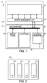
- FIG 1 is a schematic overview of a processor 10 forming an exemplary embodiment of the present invention.
- the processor 10 includes a processing engine 100 and a processor backplane 20.
- the processor is a Digital Signal Processor 10 implemented in an Application Specific Integrated Circuit (ASIC).
- ASIC Application Specific Integrated Circuit
- the processing engine 100 forms a central processing unit (CPU) with a processing core 102 and a memory interface, or management, unit 104 for interfacing the processing core 102 with memory units external to the processor core 102.
- CPU central processing unit
- management unit 104 for interfacing the processing core 102 with memory units external to the processor core 102.
- the processor backplane 20 comprises a backplane bus 22, to which the memory management unit 104 of the processing engine is connected. Also connected to the backplane bus 22 is an instruction cache memory 24, peripheral devices 26 and an external interface 28.
- the processing engine 100 could form the processor 10, with the processor backplane 20 being separate therefrom.
- the processing engine 100 could, for example be a DSP separate from and mounted on a backplane 20 supporting a backplane bus 22, peripheral and external interfaces.
- the processing engine 100 could, for example, be a microprocessor rather than a DSP and could be implemented in technologies other than ASIC technology.
- the processing engine, or a processor including the processing engine could be implemented in one or more integrated circuits.
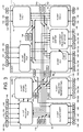
- FIG. 2 illustrates the basic structure of an embodiment of the processing core 102.
- the processing core 102 includes four elements, namely an Instruction Buffer Unit (I Unit) 106 and three execution units.
- the execution units are a Program Flow Unit (P Unit) 108, Address Data Flow Unit (A Unit) 110 and a Data Computation Unit (D Unit) 112 for executing instructions decoded from the Instruction Buffer Unit (I Unit) 106 and for controlling and monitoring program flow.
- P Unit Program Flow Unit
- a Unit Address Data Flow Unit
- D Unit Data Computation Unit
- FIG. 3 illustrates the P Unit 108, A Unit 110 and D Unit 112 of the processing core 102 in more detail and shows the bus structure connecting the various elements of the processing core 102.
- the P Unit 108 includes, for example, loop control circuitry, GoTo/Branch control circuitry and various registers for controlling and monitoring program flow such as repeat counter registers and interrupt mask, flag or vector registers.
- the P Unit 108 is coupled to general purpose Data Write busses (EB, FB) 130, 132, Data Read busses (CB, DB) 134, 136 and a coefficient program bus (BB) 138. Additionally, the P Unit 108 is coupled to sub-units within the A Unit 110 and D Unit 112 via various busses labeled CSR, ACB and RGD.
- the A Unit 110 includes a register file 30, a data address generation sub-unit (DAGEN) 32 and an Arithmetic and Logic Unit (ALU) 34.
- the A Unit register file 30 includes various registers, among which are 16 bit pointer registers (AR0, ..., AR7) and data registers (DR0, ..., DR3) which may also be used for data flow as well as address generation. Additionally, the register file includes 16 bit circular buffer registers and 7 bit data page registers.
- the general purpose busses (EB, FB, CB, DB) 130, 132, 134, 136, a coefficient data bus 140 and a coefficient address bus 142 are coupled to the A Unit register file 30.
- the A Unit register file 30 is coupled to the A Unit DAGEN unit 32 by unidirectional busses 144 and 146 respectively operating in opposite directions.
- the DAGEN unit 32 includes 16 bit X/Y registers and coefficient and stack pointer registers, for example for controlling and monitoring address generation within the processing engine 100.
- the A Unit 110 also comprises the ALU 34 which includes a shifter function as well as the functions typically associated with an ALU such as addition, subtraction, and AND, OR and XOR logical operators.
- the ALU 34 is also coupled to the general-purpose busses (EB, DB) 130, 136 and an instruction constant data bus (KDB) 140.
- the A Unit ALU is coupled to the P Unit 108 by a PDA bus for receiving register content from the P Unit 108 register file.
- the ALU 34 is also coupled to the A Unit register file 30 by busses RGA and RGB for receiving address and data register contents and by a bus RGD for forwarding address and data registers in the register file 30.
- the D Unit 112 includes a D Unit register file 36, a D Unit ALU 38, a D Unit shifter 40 and two multiply and accumulate units (MAC1, MAC2) 42 and 44.
- the D Unit register file 36, D Unit ALU 38 and D Unit shifter 40 are coupled to busses (EB, FB, CB, DB and KDB) 130, 132, 134, 136 and 140, and the MAC units 42 and 44 are coupled to the busses (CB, DB, KDB) 134, 136, 140 and data read bus (BB) 144.
- the D Unit register file 36 includes 40-bit accumulators (AC0, ..., AC3) and a 16-bit transition register.
- the D Unit 112 can also utilize the 16 bit pointer and data registers in the A Unit 110 as source or destination registers in addition to the 40-bit accumulators.
- the D Unit register file 36 receives data from the D Unit ALU 38 and MACs 1&2 42, 44 over accumulator write busses (ACW0, ACW1) 146, 148, and from the D Unit shifter 40 over accumulator write bus (ACW1) 148. Data is read from the D Unit register file accumulators to the D Unit ALU 38, D Unit shifter 40 and MACs 1&2 42, 44 over accumulator read busses (ACR0, ACR1) 150, 152.
- the D Unit ALU 38 and D Unit shifter 40 are also coupled to sub-units of the A Unit 108 via various busses labeled EFC, DRB, DR2 and ACB.
- an instruction buffer unit 106 comprising a 32 word instruction buffer queue (IBQ) 502.
- the IBQ 502 comprises 32 ⁇ 16 bit registers 504, logically divided into 8 bit bytes 506. Instructions arrive at the IBQ 502 via the 32-bit program bus (PB) 122.
- the instructions are fetched in a 32-bit cycle into the location pointed to by the Local Write Program Counter (LWPC) 532.
- the LWPC 532 is contained in a register located in the P Unit 108.
- the P Unit 108 also includes the Local Read Program Counter (LRPC) 536 register, and the Write Program Counter (WPC) 530 and Read Program Counter (RPC) 534 registers.
- LRPC Local Read Program Counter
- WPC Write Program Counter
- RPC Read Program Counter
- LRPC 536 points to the location in the IBQ 502 of the next instruction or instructions to be loaded into the instruction decoder(s) 512 and 514. That is to say, the LRPC 534 points to the location in the IBQ 502 of the instruction currently being dispatched to the decoders 512, 514.
- the WPC points to the address in program memory of the start of the next 4 bytes of instruction code for the pipeline. For each fetch into the IBQ, the next 4 bytes from the program memory are fetched regardless of instruction boundaries.
- the RPC 534 points to the address in program memory of the instruction currently being dispatched to the decoder(s) 512 and 514.
- the instructions are formed into a 48-bit word and are loaded into the instruction decoders 512, 514 over a 48-bit bus 516 via multiplexors 520 and 521. It will be apparent to a person of ordinary skill in the art that the instructions may be formed into words comprising other than 48-bits, and that the present invention is not limited to the specific embodiment described above.
- the bus 516 can load a maximum of two instructions, one per decoder, during any one instruction cycle.
- the combination of instructions may be in any combination of formats, 8, 16, 24, 32, 40 and 48 bits, which will fit across the 48-bit bus.
- Decoder 1, 512 is loaded in preference to decoder 2, 514, if only one instruction can be loaded during a cycle.
- the respective instructions are then forwarded on to the respective function units in order to execute them and to access the data for which the instruction or operation is to be performed.
- the instructions Prior to being passed to the instruction decoders, the instructions are aligned on byte boundaries. The alignment is done based on the format derived for the previous instruction during decoding thereof.
- the multiplexing associated with the alignment of instructions with byte boundaries is performed in multiplexors 520 and 521.
- the processor core 102 executes instructions through a 7 stage pipeline, the respective stages of which will now be described with reference to Figure 5.
- the first stage of the pipeline is a PRE-FETCH (P0) stage 202, during which stage a next program memory location is addressed by asserting an address on the address bus (PAB) 118 of a memory interface, or memory management unit 104.
- P0 PRE-FETCH
- PAB address bus
- FETCH (P1) stage 204 the program memory is read and the I Unit 106 is filled via the PB bus 122 from the memory management unit 104.
- the PRE-FETCH and FETCH stages are separate from the rest of the pipeline stages in that the pipeline can be interrupted during the PRE-FETCH and FETCH stages to break the sequential program flow and point to other instructions in the program memory, for example for a Branch instruction.
- the next instruction in the instruction buffer is then dispatched to the decoder/s 512/514 in the third stage, DECODE (P2) 206, where the instruction is decoded and dispatched to the execution unit for executing that instruction, for example to the P Unit 108, the A Unit 110 or the D Unit 112.
- the decode stage 206 includes decoding at least part of an instruction including a first part indicating the class of the instruction, a second part indicating the format of the instruction and a third part indicating an addressing mode for the instruction.
- the next stage is an ADDRESS (P3) stage 208, in which the address of the data to be used in the instruction is computed, or a new program address is computed should the instruction require a program branch or jump. Respective computations take place in the A Unit 110 or the P Unit 108 respectively.
- ADDRESS P3 stage 208
- an ACCESS (P4) stage 210 the address of a read operand is output and the memory operand, the address of which has been generated in a DAGEN X operator with an Xmem indirect addressing mode, is then READ from indirectly addressed X memory (Xmem).
- the next stage of the pipeline is the READ (P5) stage 212 in which a memory operand, the address of which has been generated in a DAGEN Y operator with an Ymem indirect addressing mode or in a DAGEN C operator with coefficient address mode, is READ.
- the address of the memory location to which the result of the instruction is to be written is output.
- read operands can also be generated in the Y path, and write operands in the X path.
- stage 214 there is an execution EXEC (P6) stage 214 in which the instruction is executed in either the A Unit 110 or the D Unit 112. The result is then stored in a data register or accumulator, or written to memory for Read/Modify/Write or store instructions. Additionally, shift operations are performed on data in accumulators during the EXEC stage.
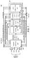
- the present embodiment of the invention includes a memory management unit 104 which is coupled to external memory units via a 24 bit address bus 114 and a bi-directional 16 bit data bus 116. Additionally, the memory management unit 104 is coupled to program storage memory (not shown) via a 24 bit address bus 118 and a 32 bit bi-directional data bus 120. The memory management unit 104 is also coupled to the I Unit 106 of the machine processor core 102 via a 32 bit program read bus (PB) 122. The P Unit 108, A Unit 110 and D Unit 112 are coupled to the memory management unit 104 via data read and data write busses and corresponding address busses. The P Unit 108 is further coupled to a program address bus 128.
- PB program read bus
- the P Unit 108 is coupled to the memory management unit 104 by a 24 bit program address bus 128, the two 16 bit data write busses (EB, FB) 130, 132, and the two 16 bit data read busses (CB, DB) 134, 136.
- the A Unit 110 is coupled to the memory management unit 104 via two 24 bit data write address busses (EAB, FAB) 160, 162, the two 16 bit data write busses (EB, FB) 130, 132, the three data read address busses (BAB, CAB, DAB) 164, 166, 168 and the two 16 bit data read busses (CB, DB) 134, 136.
- the D Unit 112 is coupled to the memory management unit 104 via the two data write busses (EB, FB) 130, 132 and three data read busses (BB, CB, DB) 144, 134, 136.
- Figure 7 represents the passing of instructions from the I Unit 106 to the P Unit 108 at 124, for forwarding branch instructions for example. Additionally, Figure 7 represents the passing of data from the I Unit 106 to the A Unit 110 and the D Unit 112 at 126 and 128 respectively.
- a difficulty with the operation of a pipeline is that different instructions may need to make access to one and the same resource. Quite often, a first instruction will be operable to modify a resource, for example a register of a part, for example a field, of a register and a second instruction may then need to access that resource. If the instructions were being processed separately with the processing of the second instruction only being commenced when the processing of the first instruction has finished, this would not create a conflict. However, in a pipelined architecture, there is a possibility that a second instruction could access the resource before the first instruction has finished with it, unless measures are undertaken to prevent this.
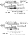
- FIG. 8A represents an example of a pipeline protection action for a Read After Write (RAW).
- a pipeline protection action (604) comprises setting a stall 606 for the address phase, whereby the addresses for the read are not generated at 610 (the read of AR1 is not valid) until after the write to AR1 is performed at 612, the new AR1 value being available and the stall for the address phase being relaxed (removed) at 614.
- FIG. 8B represents another example of a pipeline protection action for a Read After Write (RAW).
- Step 602 represents a read performed in the read phase (RD) on AR0 (e.g. Condition Read/MMR read).
- a pipeline protection action (624) comprises setting a stall 626 for the access phase (ACC), whereby the addresses and requests are kept active at 628, a write on AC0 is performed at 630 and the stall of the access phase is relaxed (removed) and the Condition/MMR new value is available at 632.
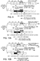
- FIG 9 represents an example of a pipeline protection action for a Write After Write (WAW).
- a pipeline protection action (644) comprises setting a stall 646 for the address phase, whereby the addresses for the second write to AR1 are not generated at 650 (the write to AR1 is not allowed) until after the first write to AR1 is performed at 652, the new AR1 value being available and the stall for the address phase being relaxed (removed) at 654.
- FIG 10A represents an example of a pipeline protection action for a Write After Read (WAR).
- Step 662 represents a write performed in the address phase (ADR) on AR3 (e.g. *AR3+DR0).
- a pipeline protection action (664) comprises setting a stall 666 for the address phase, whereby the addresses for the write to AR3 are not generated at 670 (the write to AR3 is not allowed) until after the read of AR3 is performed at 672, the AR3 write being allowed and the stall for the address phase being relaxed (removed) at 674.
- FIG 10B represents another example of a pipeline protection action for a Write After Read (WAR).
- Step 680 represents a read performed by a first instruction in a read phase (RD) on a register AR3 (e.g. Condition or MMR).
- Step 682 represents a write performed in the address phase (ADR) on AR3 (e.g. *AR3 + DR0).
- a pipeline protection action (684) comprises setting a stall 686 for the address phase, whereby the addresses for the write to AR3 are not generated at 690 (the write to AR3 is not allowed) until after the read of AR3 is performed at 690, the write to AR3 then being allowed and the stall for the address phase being relaxed (removed).
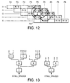
- Figure 11 is a schematic of an approach adopted for determining a definition of a generic arbitration function of all possible resource access conflicts of the pipeline.
- the generic arbitration function is an abstract concept which underpins and simplifies the design of each arbitration logic, which can all be implemented as special forms of the generic function.
- Logic in which the generic arbitration function is embedded may also be included in the processing engine.
- the generic arbitration function can also aid circuit testing at the end of the circuit design. Although described in the context of the present embodiment, this approach could be used for other processor architectures.
- register files e.g. 702, 704, 706
- register files e.g. 702, 704, 706
- CF program unit
- DU data unit
- AU address unit
- Each of the register files comprises a number of registers N(i) (e.g., 708, 710, 712).
- N(i) e.g., 708, 710, 712).
- These registers can form the resources to be protected.
- it may be desired to protect parts of (or fields within) registers e.g. 714, 716, 718).
- Figure 11 represents this definition of resource granularity. Accordingly, a protected resource could, for example, be a register or a field within a register.
- the pipeline depth (e.g., here pipeline stages P2, P3, P4, P5 and P6) has to be taken into account to consider the instruction execution overlap, as represented at 722 for five instructions I0, I1, I2, I3 and I4.
- Figure 12 is a schematic diagram illustrating potential conflicts at different stages of a pipeline.
- Figure 12 illustrates the five stages P2 - P6 of Figure 5 for each of the four instructions I0, I1, I2 and I3 and I4.
- a generic arbitration function can be derived as illustrated in Figure 13, this generic arbitration function defining relationships between current and pending accesses.
- the generic arbitration function can then be used to control the selective stalling of the pipeline to avoid data hazards.
- the generic logic is representative of all potential resource access conflicts for the pipeline. From an analysis of the potential conflict problems represented schematically in Figure 12, the following signals susceptible to resulting in a conflict can be identified, namely:
- each arbitration logic will be a special form or sub-set of the generic function with a lower degree of degeneracy, i.e. with a number of the operands which are variable in the generic function being fixed.
- the generic arbitration function can be used to implement the circuit design of each of the arbitration logic blocks, which are all definable as special forms of the generic arbitration function.
- the full generic form is not needed for the arbitration logic of each individual resource, since, for each of the resources, it will in general be impossible for some of the conflicts envisaged by the generic arbitration function to occur.
- Generic arbitration logic embodying the generic arbitration function need only be provided in the processing engine if full protection is desired against simultaneous occurrence of all envisaged conflicts.
- the concept of the generic arbitration function can be further exploited at the stage of software testing of the hardware design of the processing engine.
- generating all the test patterns for pipeline processing engine hardware can be a huge undertaking because of the complexity of the CPU, its instruction set and architecture.
- the test patterns need to be defined in terms of a prespecified reference. It is the specification of this reference which can be highly laborious.
- a functional test pattern generator can be created using the generic function as the reference in association with a conventional instruction set latency table. This simplifies the creation of the test pattern generator since the scope of the testing can be restricted to the possible conflicts envisaged by the generic function. Because the test pattern generator follows directly from the generic function, the process of hardware design testing is not only quicker, but also more systematic and ensures good coverage.
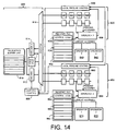
- Figure 14 is a schematic overview of an interlocked architecture for a processing engine. As shown in Figure 14, there are first and second pipelines 820 and 850, receiving instructions from a control flow 800. In terms of Figure 2, the first pipeline could be the D unit and the second pipeline could be the A unit, for example.
- the control flow includes an instruction buffer 810 and first and second decoders 812 and 814, for decoding first and second instruction streams.
- a parallel encoding validity check is effected in parallel verification logic 816, to ensure that the parallel context is valid.
- the instructions from the decoders 812 and 814 are dispatched from dispatch logic 818 under the control of a dispatch controller 808.
- first pipeline 820 successive pipeline stages 822, 824, 826 and 828 are under the control of a local pipeline controller 830.
- first local interlock control logic 838 forming a first local interlock controller.
- the pipeline controller is responsive to control signals from the associated interlock control logic to cause selective stalling of the pipelines stages. This is responsive to outputs from the pipeline 820 and also to outputs from a register file 832 for the pipeline 820.
- the register file 832 includes register file control logic 834 and individual registers 836.
- One or more operators 840 and 842 may be accessed in respect of a current access operation.
- successive pipeline stages 852, 854, 856 and 858 are under the control of a local pipeline controller 860.
- second local interlock control logic 868 forming a second local interlock controller.
- the pipeline controller is responsive to control signals from the associated interlock control logic to cause selective stalling of the pipeline stages. This is responsive to outputs from the pipeline 850 and also to outputs from a register file 862 for the pipeline 850.
- the register file 862 includes register file control logic 864 and individual registers 866.
- One or more operators 870 and 872 may be accessed in respect of a current access operation.
- each of the local pipeline controllers 830 and 860 is responsive to outputs from each of the local interlock controllers 838 and 868. This general principle is extendible. Accordingly, where more than two pipelines are provided, the local pipeline controller for each pipeline will be responsive to the outputs from all of the local interrupt controllers.
- FIG 15 A schematic overview of an exemplary structure for an interlock control mechanism is illustrated in Figure 15, for example, for the pipelines 820 of Figure 14. It will be understood that the mechanism could have the same structure for other pipelines, such as the pipeline 850 of Figure 14. It will be noted that no memory elements (read/write queue) are provided for stall management as the instruction pipeline itself is used to achieve this. For example, a write after write conflict from stage P4 to stage P7 of the pipeline between two consecutive instructions should generate a 3 cycle stall (at stage 4). In practice, the interlock logic generates 3 x 1 cycle consecutive stalls (at stage 4).
- Figure 15 illustrates a regular and parallel structure for hazard detection, including:
- the stall control signals 889 are also supplied to register access control logic 890 current access control. Stall penalty reduction is not considered in this architecture, with the result that any conflict will result in an appropriate pipeline stall, that is a freeze of the lower stages and bubble insertion at the next stage.
- the arbitration logic is relatively simple in hardware as a result of its 'logic re-use'.
- logic re-use it is meant that the arbitration logic makes use of tapping from the queue of the existing main pipeline 822 - 828 (rather than creation of a new queue for arbitration purposes which has been previously proposed) and also makes use of the results from the decoders 880, in the embodiment through the merge logic 883. Consequently, the additional amount of hardware required for the arbitration logic blocks is greatly reduced.
- all the arbitration logic covers less than 2% of the total CPU area.
- the chip area required for the logic necessary to provide a comparable level of pipeline protection would be at least several times greater, perhaps an order of magnitude greater.
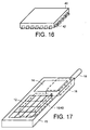
- Figure 16 is a schematic representation of an integrated circuit 40 incorporating the processor 10 of Figure 1.
- the integrated circuit can be implemented using application specific integrated circuit (ASIC) technology.
- ASIC application specific integrated circuit
- the integrated circuit includes a plurality of contacts 42 for surface mounting.
- the integrated circuit could include other configurations, for example a plurality of pins on a lower surface of the circuit for mounting in a zero insertion force socket, or indeed any other suitable configuration.
- a processing engine such as the processor 10, for example as incorporated in an integrated circuit as in Figure 16, is in a telecommunications device, for example a mobile wireless telecommunications device.
- Figure 17 illustrates one example of such a telecommunications device.
- the telecommunications device is a mobile telephone 11 with integrated user input device such as a keypad, or keyboard 12 and a display 14.
- the display could be implemented using appropriate technology, as, for example, a liquid crystal display or a TFT display.
- the processor 10 is connected to the keypad 12, where appropriate via a keyboard adapter (not shown), to the display 14, where appropriate via a display adapter (not shown), and to a telecommunications interface or transceiver 16, for example a wireless telecommunications interface including radio frequency (RF) circuitry.
- the radio frequency circuitry could be incorporated into, or separate from, an integrated circuit 40 comprising the processor 10.
- the RF circuitry 16 is connected to an aerial 18.
Abstract
Description
- The present invention relates to pipeline processor design, more especially to protecting a processor pipeline against conflicts.
- Typically, modem processing engines, such as are found in digital signal processors (DSP's) or microprocessors employ a pipelined architecture in order to improve processing performance. A pipelined architecture means that various stages of instruction processing are performed sequentially such that more than one instruction will be at different stages of processing within the pipeline at any one stage.
- Although a pipelined architecture does allow higher processing speed than would be possible if the processing of one instruction were to be completed before the processing of another could be started, this does lead to significant complications regarding potential conflicts in operation. Conflicts may occur between resource accesses, for example in a situation where a second instruction attempts to access a register or a part of a register before a first instruction has finished operations on that register, whereby the second instruction might receive invalid data.
- Such potential conflicts are often termed "data hazards". Examples of possible data hazards are in cases of, for example:
- read after write (ex:
- write after read (ex:
- write after write (ex:
- Various techniques for hardware pipeline protection are known in the art.
- One example is termed "scoreboarding". With scoreboarding each register or field can have pending writes and reads qualified with their execution phase using a table, or scoreboard. However, such an approach can be complex to handle and expensive in terms of logic overhead and, as a consequence, in power consumption. Particularly in processing engines designed for portable applications or applications powered other than by the mains (e.g., battery or other alternatively powered applications), such an approach is undesirable. Moreover, a scoreboarding approach rapidly becomes unwieldy when the processing engine has a large instruction set and/or a parallel processing architecture.
- Other approaches can employ read/write queuing. However, such an approach is unsuitable where there is a wide variety of pipeline fields and/or sources of resource accesses. Moreover, such an approach can also rapidly become complex to handle and expensive in terms of logic overhead and power consumption.
- A further approach can employ attaching a resource encoding to instructions within the pipeline. However, such an approach can also suffer from disadvantages similar to those described above.
- There is, therefore, is a need for a different approach to resource conflict management within a pipeline for avoiding data hazards, which does not suffer from the disadvantages of the prior approaches described above.
- Particular and preferred aspects of the invention are set out in the accompanying independent and dependent claims. Combinations of features from the dependent claims may be combined with features of the independent claims as appropriate and not merely as explicitly set out in the claims.
- In accordance with an aspect of the invention, there is provided a processing engine including a processor pipeline with a plurality of pipeline stages, a plurality of resources and a pipeline protection mechanism. The pipeline protection mechanism includes, for each protected resource, respective arbitration logic for anticipating access conflicts for that resource between the pipeline stages. An output of each arbitration logic is connected to form stall control signals for controlling the selective stalling of the pipeline to avoid the resource access conflicts.
- The resources could, for example, be registers or parts (e.g. fields) of registers.
- By providing arbitration logic for each resource, an embodiment of the invention effectively enables a distribution of the control logic needed to anticipate potential resource access conflicts, and allows selectively stalling of the pipeline to avoid the conflicts from actually occurring. With this distributed, or modular, approach the overall logic can be kept relatively simple and easy to manage. Also, surprisingly, this can result in a reduction in the total logic needed. Consequently, less area, or so-called real estate, within an integrated circuit will be taken up by the pipeline protection mechanism than would be the case with the prior approaches described above. Moreover, as a result of the reduction in the amount of logic needed, the power consumption can be reduced, while still providing effective pipeline protection.
- Preferably, the arbitration logic for each of the resources is derived from a generic arbitration logic determined for the pipeline. The generic function may itself be embodied in the integrated circuit as generic arbitration logic capable of handling simultaneous occurrence of all envisaged conflicts. Each of the arbitration logic blocks may fully embody the generic arbitration function, but will typically only embody different special forms of the generic arbitration function. The generic arbitration function provides a logical definition of all of the potential, or theoretical, conflicts which could occur between respective pipeline stages. In practice, it may not be physically possible for all of the theoretical conflicts to occur for each of the resources, since the resources concerned may not be accessible at all of the pipeline stages being monitored. However, configuring the respective arbitration logic blocks from a single, generic function simplifies the design of the logic for the individual resources, and provides consistent performance and testability.
- The processing engine will typically include pipeline control logic for controlling the stages of the pipeline. This pipeline control logic can be connected to receive the stall control signals derived, or output, from the arbitration logic. Output merge logic can be provided for merging the output of each arbitration logic to form stall control signals for controlling the selective stalling of the pipeline to avoid the resource access conflicts.
- The pipeline protection mechanism may comprise an access decoder stage connected to receive access information from at least selected pipeline stages to derive access information for respective protected resources. The arbitration logic for a protected resource can then be connected to receive access information for that protected resource from the access decoder stage. In this manner, the arbitration logic for each protected resource can receive the information it needs to perform a conflict check for that resource.
- The decoder stage may include a plurality of access decoders, each access decoder being associated with a respective pipeline stage. Input merge logic can be provided for each protected resource to merge the access information for that resource from the various access decoders.
- The access information can relate to pending accesses. It can also relate to current access. Indeed, a current access decoding stage can be connected to receive current access information from the pipeline to derive current access information for respective protected resources, the arbitration logic for a protected resource being connected to receive current access information for that protected resource as well as pending access information.
- In an embodiment of the invention, the current access decoder stage is a decoder stage for a register file, whereby the logic for the register file is reused for the pipeline protection mechanism, thus providing a saving in the logic required for the processing engine.
- Separate input merge logic can be provided for each protected resource and be connected to the arbitration logic for that resource.
- The processing engine can be in the form of a digital signal processor. Alternatively, it could be in the form of a microprocessor, or any other form of processing engine employing a pipelined architecture. The processing engine can be implemented in the form of an integrated circuit.
- A particular application for a processing engine in accordance with the present invention is in the form of a wireless telecommunications device, in particular a portable telecommunications device such as, for example, a mobile telephone, where low power consumption and high processing performance is required.
- In accordance with another aspect of the invention there is provided a method of protecting a pipeline in a processing engine, which processing engine includes a processor pipeline with a plurality of pipeline stages and a plurality of resources. The method comprises, for respective protected resources, separately arbitrating for the resource to anticipate access conflicts between the pipeline stages, and selectively stalling the pipeline depending upon the result of the arbitration for the respective resources to avoid resource access conflicts.
- Particular embodiments in accordance with the invention will now be described, by way of example only, and with reference to the accompanying drawings in which like reference signs are used to denote like pans, unless otherwise stated, and in which:
- Figure 1 is a schematic block diagram of a processor in accordance with an embodiment of the invention;
- Figure 2 is a schematic diagram of a core of the processor of Figure 1;
- Figure 3 is a more detailed schematic block diagram of various execution units of the core of the processor of Figure 1;
- Figure 4 is schematic diagram of an instruction buffer queue and an instruction decoder controller of the processor of Figure 1;
- Figure 5 is a representation of pipeline phases of the processor of Figure 1;
- Figure 6 is a diagrammatic illustration of an example of operation of a pipeline in the processor of Figure 1;
- Figure 7 is a schematic representation of the core of the processor for explaining the operation of the pipeline of the processor of Figure 1;
- Figure 8A is an example of a read after write hazard;
- Figure 8B is another example of a read after write hazard;
- Figure 9 is an example of a write after write hazard;
- Figure 10A is one example of a write after read hazard;
- Figure 10B is another example of a write after read hazard;
- Figure 11 illustrates possible conflicts at various pipeline stages;
- Figure 12 illustrates the derivation of a generic arbitration function definition process;
- Figure 13 is a schematic diagram of generic arbitration logic;
- Figure 14 illustrates the architecture of a dual-pipeline arithmetic logic unit of a processing engine incorporating an embodiment of the invention;
- Figure 15 is a schematic block diagram of an example of pipeline protection logic in accordance with the invention;
- Figure 16 is an integrated circuit incorporating the processor of Figure 1; and
- Figure 17 is an example of mobile telecommunications apparatus incorporating the processor of Figure 1.
-
- Although the invention finds particular application to Digital Signal Processors (DSPs), implemented for example in an Application Specific Integrated Circuit (ASIC), it also finds application to other forms of processing engines.
- The basic architecture of an example of a processor according to the invention will now be described.
- Figure 1 is a schematic overview of a
processor 10 forming an exemplary embodiment of the present invention. Theprocessor 10 includes aprocessing engine 100 and aprocessor backplane 20. In the present embodiment, the processor is aDigital Signal Processor 10 implemented in an Application Specific Integrated Circuit (ASIC). - As shown in Figure 1, the
processing engine 100 forms a central processing unit (CPU) with aprocessing core 102 and a memory interface, or management,unit 104 for interfacing theprocessing core 102 with memory units external to theprocessor core 102. - The
processor backplane 20 comprises a backplane bus 22, to which thememory management unit 104 of the processing engine is connected. Also connected to the backplane bus 22 is aninstruction cache memory 24,peripheral devices 26 and anexternal interface 28. - It will be appreciated that in other embodiments, the invention could be implemented using different configurations and/or different technologies. For example, the
processing engine 100 could form theprocessor 10, with theprocessor backplane 20 being separate therefrom. Theprocessing engine 100 could, for example be a DSP separate from and mounted on abackplane 20 supporting a backplane bus 22, peripheral and external interfaces. Theprocessing engine 100 could, for example, be a microprocessor rather than a DSP and could be implemented in technologies other than ASIC technology. The processing engine, or a processor including the processing engine, could be implemented in one or more integrated circuits. - Figure 2 illustrates the basic structure of an embodiment of the
processing core 102. As illustrated, theprocessing core 102 includes four elements, namely an Instruction Buffer Unit (I Unit) 106 and three execution units. The execution units are a Program Flow Unit (P Unit) 108, Address Data Flow Unit (A Unit) 110 and a Data Computation Unit (D Unit) 112 for executing instructions decoded from the Instruction Buffer Unit (I Unit) 106 and for controlling and monitoring program flow. - Figure 3 illustrates the
P Unit 108, AUnit 110 andD Unit 112 of theprocessing core 102 in more detail and shows the bus structure connecting the various elements of theprocessing core 102. TheP Unit 108 includes, for example, loop control circuitry, GoTo/Branch control circuitry and various registers for controlling and monitoring program flow such as repeat counter registers and interrupt mask, flag or vector registers. TheP Unit 108 is coupled to general purpose Data Write busses (EB, FB) 130, 132, Data Read busses (CB, DB) 134, 136 and a coefficient program bus (BB) 138. Additionally, theP Unit 108 is coupled to sub-units within theA Unit 110 andD Unit 112 via various busses labeled CSR, ACB and RGD. - As illustrated in Figure 3, in the present embodiment the
A Unit 110 includes aregister file 30, a data address generation sub-unit (DAGEN) 32 and an Arithmetic and Logic Unit (ALU) 34. The AUnit register file 30 includes various registers, among which are 16 bit pointer registers (AR0, ..., AR7) and data registers (DR0, ..., DR3) which may also be used for data flow as well as address generation. Additionally, the register file includes 16 bit circular buffer registers and 7 bit data page registers. As well as the general purpose busses (EB, FB, CB, DB) 130, 132, 134, 136, acoefficient data bus 140 and acoefficient address bus 142 are coupled to the AUnit register file 30. The AUnit register file 30 is coupled to the AUnit DAGEN unit 32 byunidirectional busses DAGEN unit 32 includes 16 bit X/Y registers and coefficient and stack pointer registers, for example for controlling and monitoring address generation within theprocessing engine 100. - The
A Unit 110 also comprises theALU 34 which includes a shifter function as well as the functions typically associated with an ALU such as addition, subtraction, and AND, OR and XOR logical operators. TheALU 34 is also coupled to the general-purpose busses (EB, DB) 130, 136 and an instruction constant data bus (KDB) 140. The A Unit ALU is coupled to theP Unit 108 by a PDA bus for receiving register content from theP Unit 108 register file. TheALU 34 is also coupled to the AUnit register file 30 by busses RGA and RGB for receiving address and data register contents and by a bus RGD for forwarding address and data registers in theregister file 30. - As illustrated, the
D Unit 112 includes a DUnit register file 36, aD Unit ALU 38, aD Unit shifter 40 and two multiply and accumulate units (MAC1, MAC2) 42 and 44. The DUnit register file 36,D Unit ALU 38 andD Unit shifter 40 are coupled to busses (EB, FB, CB, DB and KDB) 130, 132, 134, 136 and 140, and theMAC units Unit register file 36 includes 40-bit accumulators (AC0, ..., AC3) and a 16-bit transition register. TheD Unit 112 can also utilize the 16 bit pointer and data registers in theA Unit 110 as source or destination registers in addition to the 40-bit accumulators. The DUnit register file 36 receives data from theD Unit ALU 38 and MACs 1&2 42, 44 over accumulator write busses (ACW0, ACW1) 146, 148, and from theD Unit shifter 40 over accumulator write bus (ACW1) 148. Data is read from the D Unit register file accumulators to theD Unit ALU 38,D Unit shifter 40 and MACs 1&2 42, 44 over accumulator read busses (ACR0, ACR1) 150, 152. TheD Unit ALU 38 andD Unit shifter 40 are also coupled to sub-units of theA Unit 108 via various busses labeled EFC, DRB, DR2 and ACB. - Referring now to Figure 4, there is illustrated an
instruction buffer unit 106 comprising a 32 word instruction buffer queue (IBQ) 502. TheIBQ 502 comprises 32×16 bit registers 504, logically divided into 8 bit bytes 506. Instructions arrive at theIBQ 502 via the 32-bit program bus (PB) 122. The instructions are fetched in a 32-bit cycle into the location pointed to by the Local Write Program Counter (LWPC) 532. TheLWPC 532 is contained in a register located in theP Unit 108. TheP Unit 108 also includes the Local Read Program Counter (LRPC) 536 register, and the Write Program Counter (WPC) 530 and Read Program Counter (RPC) 534 registers.LRPC 536 points to the location in theIBQ 502 of the next instruction or instructions to be loaded into the instruction decoder(s) 512 and 514. That is to say, theLRPC 534 points to the location in theIBQ 502 of the instruction currently being dispatched to thedecoders RPC 534 points to the address in program memory of the instruction currently being dispatched to the decoder(s) 512 and 514. - The instructions are formed into a 48-bit word and are loaded into the
instruction decoders bit bus 516 viamultiplexors - The
bus 516 can load a maximum of two instructions, one per decoder, during any one instruction cycle. The combination of instructions may be in any combination of formats, 8, 16, 24, 32, 40 and 48 bits, which will fit across the 48-bit bus.Decoder decoder multiplexors - The
processor core 102 executes instructions through a 7 stage pipeline, the respective stages of which will now be described with reference to Figure 5. - The first stage of the pipeline is a PRE-FETCH (P0)
stage 202, during which stage a next program memory location is addressed by asserting an address on the address bus (PAB) 118 of a memory interface, ormemory management unit 104. - In the next stage, FETCH (P1)
stage 204, the program memory is read and theI Unit 106 is filled via thePB bus 122 from thememory management unit 104. - The PRE-FETCH and FETCH stages are separate from the rest of the pipeline stages in that the pipeline can be interrupted during the PRE-FETCH and FETCH stages to break the sequential program flow and point to other instructions in the program memory, for example for a Branch instruction.
- The next instruction in the instruction buffer is then dispatched to the decoder/s 512/514 in the third stage, DECODE (P2) 206, where the instruction is decoded and dispatched to the execution unit for executing that instruction, for example to the
P Unit 108, theA Unit 110 or theD Unit 112. Thedecode stage 206 includes decoding at least part of an instruction including a first part indicating the class of the instruction, a second part indicating the format of the instruction and a third part indicating an addressing mode for the instruction. - The next stage is an ADDRESS (P3)
stage 208, in which the address of the data to be used in the instruction is computed, or a new program address is computed should the instruction require a program branch or jump. Respective computations take place in theA Unit 110 or theP Unit 108 respectively. - In an ACCESS (P4)
stage 210 the address of a read operand is output and the memory operand, the address of which has been generated in a DAGEN X operator with an Xmem indirect addressing mode, is then READ from indirectly addressed X memory (Xmem). - The next stage of the pipeline is the READ (P5)
stage 212 in which a memory operand, the address of which has been generated in a DAGEN Y operator with an Ymem indirect addressing mode or in a DAGEN C operator with coefficient address mode, is READ. The address of the memory location to which the result of the instruction is to be written is output. - In the case of dual access, read operands can also be generated in the Y path, and write operands in the X path.
- Finally, there is an execution EXEC (P6)
stage 214 in which the instruction is executed in either theA Unit 110 or theD Unit 112. The result is then stored in a data register or accumulator, or written to memory for Read/Modify/Write or store instructions. Additionally, shift operations are performed on data in accumulators during the EXEC stage. - The basic principle of operation for a pipeline processor will now be described with reference to Figure 6. As can be seen from Figure 6, for a
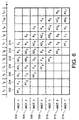
first instruction 302, the successive pipeline stages take place over time periods T1-T7. Each time period is a clock cycle for the processor machine clock. Asecond instruction 304, can enter the pipeline in period T2, since the previous instruction has now moved on to the next pipeline stage. Forinstruction PRE-FETCH stage 202 occurs in time period T3. As can be seen from Figure 6 for a seven stage pipeline a total of 7 instructions may be processed simultaneously. For all 7 instructions 302-314, Figure 6 shows them all under process in time period T7. Such a structure adds a form of parallelism to the processing of instructions. - As shown in Figure 7, the present embodiment of the invention includes a
memory management unit 104 which is coupled to external memory units via a 24bit address bus 114 and a bi-directional 16bit data bus 116. Additionally, thememory management unit 104 is coupled to program storage memory (not shown) via a 24bit address bus 118 and a 32 bitbi-directional data bus 120. Thememory management unit 104 is also coupled to theI Unit 106 of themachine processor core 102 via a 32 bit program read bus (PB) 122. TheP Unit 108, AUnit 110 andD Unit 112 are coupled to thememory management unit 104 via data read and data write busses and corresponding address busses. TheP Unit 108 is further coupled to aprogram address bus 128. - More particularly, the
P Unit 108 is coupled to thememory management unit 104 by a 24 bitprogram address bus 128, the two 16 bit data write busses (EB, FB) 130, 132, and the two 16 bit data read busses (CB, DB) 134, 136. TheA Unit 110 is coupled to thememory management unit 104 via two 24 bit data write address busses (EAB, FAB) 160, 162, the two 16 bit data write busses (EB, FB) 130, 132, the three data read address busses (BAB, CAB, DAB) 164, 166, 168 and the two 16 bit data read busses (CB, DB) 134, 136. TheD Unit 112 is coupled to thememory management unit 104 via the two data write busses (EB, FB) 130, 132 and three data read busses (BB, CB, DB) 144, 134, 136. - Figure 7 represents the passing of instructions from the
I Unit 106 to theP Unit 108 at 124, for forwarding branch instructions for example. Additionally, Figure 7 represents the passing of data from theI Unit 106 to theA Unit 110 and theD Unit 112 at 126 and 128 respectively. - A difficulty with the operation of a pipeline is that different instructions may need to make access to one and the same resource. Quite often, a first instruction will be operable to modify a resource, for example a register of a part, for example a field, of a register and a second instruction may then need to access that resource. If the instructions were being processed separately with the processing of the second instruction only being commenced when the processing of the first instruction has finished, this would not create a conflict. However, in a pipelined architecture, there is a possibility that a second instruction could access the resource before the first instruction has finished with it, unless measures are undertaken to prevent this.
- Such potential conflicts are often termed "data hazards". Examples of possible data hazards are in cases of, for example:
- Read after Write (e.g.:
- Write after Read (e.g.:
- Write after Write (e.g.:
- Figure 8A represents an example of a pipeline protection action for a Read After Write (RAW). Step 600 represents a write performed by a first instruction in an execute phase (EXE) on a register AR1 (e.g.
stall 606 for the address phase, whereby the addresses for the read are not generated at 610 (the read of AR1 is not valid) until after the write to AR1 is performed at 612, the new AR1 value being available and the stall for the address phase being relaxed (removed) at 614. - Figure 8B represents another example of a pipeline protection action for a Read After Write (RAW). Step 620 represents a write performed by a first instruction in an execute phase (EXE) on a register AR0 (e.g.
stall 626 for the access phase (ACC), whereby the addresses and requests are kept active at 628, a write on AC0 is performed at 630 and the stall of the access phase is relaxed (removed) and the Condition/MMR new value is available at 632. - Figure 9 represents an example of a pipeline protection action for a Write After Write (WAW). Step 640 represents a write performed by a first instruction in an execute phase (EXE) on a register AR1 (e.g.
stall 646 for the address phase, whereby the addresses for the second write to AR1 are not generated at 650 (the write to AR1 is not allowed) until after the first write to AR1 is performed at 652, the new AR1 value being available and the stall for the address phase being relaxed (removed) at 654. - Figure 10A represents an example of a pipeline protection action for a Write After Read (WAR). Step 660 represents a read performed by a first instruction in a read phase (RD) on a register AR3 (e.g.
stall 666 for the address phase, whereby the addresses for the write to AR3 are not generated at 670 (the write to AR3 is not allowed) until after the read of AR3 is performed at 672, the AR3 write being allowed and the stall for the address phase being relaxed (removed) at 674. - Figure 10B represents another example of a pipeline protection action for a Write After Read (WAR). Step 680 represents a read performed by a first instruction in a read phase (RD) on a register AR3 (e.g. Condition or MMR). Step 682 represents a write performed in the address phase (ADR) on AR3 (e.g. *AR3 + DR0). A pipeline protection action (684) comprises setting a
stall 686 for the address phase, whereby the addresses for the write to AR3 are not generated at 690 (the write to AR3 is not allowed) until after the read of AR3 is performed at 690, the write to AR3 then being allowed and the stall for the address phase being relaxed (removed). - Figure 11 is a schematic of an approach adopted for determining a definition of a generic arbitration function of all possible resource access conflicts of the pipeline. The generic arbitration function is an abstract concept which underpins and simplifies the design of each arbitration logic, which can all be implemented as special forms of the generic function. Logic in which the generic arbitration function is embedded may also be included in the processing engine. The generic arbitration function can also aid circuit testing at the end of the circuit design. Although described in the context of the present embodiment, this approach could be used for other processor architectures.
- Referring to Figure 11, in an initial stage the organization (700) of the processing engine as a whole is divided into groups of registers, or register files (e.g. 702, 704, 706). In the present example, three register files exist for the program unit, or control flow (CF), for the data unit (DU) and for the address unit (AU). Each of the register files comprises a number of registers N(i) (e.g., 708, 710, 712). These registers can form the resources to be protected. As well as, or instead of, protecting whole registers, it may be desired to protect parts of (or fields within) registers (e.g. 714, 716, 718). Figure 11 represents this definition of resource granularity. Accordingly, a protected resource could, for example, be a register or a field within a register.
- For each protected resource, an analysis of the worst possible resource usage is derived. Different instructions will provide different ways of reading from and writing to a resource, for example. As shown in Figure 11 in respect of register field 714, the pipeline stages represented at 720 in which read/write operations could be performed for that resource are stages P3, P5 and P6. In other words, the worst case resource usage for this resource is in respect of pipeline stages P3, P5 and P6. The above accesses can be classified in terms of their execution stages.
- The pipeline depth (e.g., here pipeline stages P2, P3, P4, P5 and P6) has to be taken into account to consider the instruction execution overlap, as represented at 722 for five instructions I0, I1, I2, I3 and I4.
- All potential data hazards are considered as represented by the arrows in Figure 12, which Figure is a schematic diagram illustrating potential conflicts at different stages of a pipeline. Figure 12 illustrates the five stages P2 - P6 of Figure 5 for each of the four instructions I0, I1, I2 and I3 and I4.
- From the consideration of the data hazards found, a generic arbitration function can be derived as illustrated in Figure 13, this generic arbitration function defining relationships between current and pending accesses. The generic arbitration function can then be used to control the selective stalling of the pipeline to avoid data hazards. The generic logic is representative of all potential resource access conflicts for the pipeline. From an analysis of the potential conflict problems represented schematically in Figure 12, the following signals susceptible to resulting in a conflict can be identified, namely:
- a:
current read stage 4 - b: pending (stage 5) read
stage 7 - c: pending (stage 5) read
stage 6 - d:
current read stage 6 - e: pending (stage 6) read
stage 7 - f:
current read stage 7 - 1:
current write stage 4 - 2: pending (stage 5)
write stage 7 - 3: pending (stage 5)
write stage 6 - 4: pending (stage 6)
write stage 7 - 5:
current write stage 6 - 6:
current write stage 7 -
- The logic for interpreting these signals is illustrated in Figure 13. It will be noted that signals "d" and "f" are not shown in Figure 13. These signals are not, however, needed as all potential conflicts dealing with a 7-stage read are solved by anticipating using the pending signals "b" and "e". Accordingly, these signals do not need to be represented in Figure 13 as any conflicts related thereto can already be predicted.
- It will thus be appreciated that in general the generic function will have a large number of variable operands and that each arbitration logic will be a special form or sub-set of the generic function with a lower degree of degeneracy, i.e. with a number of the operands which are variable in the generic function being fixed.
- Once determined, the generic arbitration function can be used to implement the circuit design of each of the arbitration logic blocks, which are all definable as special forms of the generic arbitration function. The full generic form is not needed for the arbitration logic of each individual resource, since, for each of the resources, it will in general be impossible for some of the conflicts envisaged by the generic arbitration function to occur.
- Generic arbitration logic embodying the generic arbitration function need only be provided in the processing engine if full protection is desired against simultaneous occurrence of all envisaged conflicts.
- The concept of the generic arbitration function can be further exploited at the stage of software testing of the hardware design of the processing engine. In general, generating all the test patterns for pipeline processing engine hardware can be a huge undertaking because of the complexity of the CPU, its instruction set and architecture. The test patterns need to be defined in terms of a prespecified reference. It is the specification of this reference which can be highly laborious. With the present design, a functional test pattern generator can be created using the generic function as the reference in association with a conventional instruction set latency table. This simplifies the creation of the test pattern generator since the scope of the testing can be restricted to the possible conflicts envisaged by the generic function. Because the test pattern generator follows directly from the generic function, the process of hardware design testing is not only quicker, but also more systematic and ensures good coverage.
- Figure 14 is a schematic overview of an interlocked architecture for a processing engine. As shown in Figure 14, there are first and
second pipelines control flow 800. In terms of Figure 2, the first pipeline could be the D unit and the second pipeline could be the A unit, for example. - The control flow includes an
instruction buffer 810 and first andsecond decoders parallel verification logic 816, to ensure that the parallel context is valid. The instructions from thedecoders dispatch logic 818 under the control of adispatch controller 808. - In the
first pipeline 820, successive pipeline stages 822, 824, 826 and 828 are under the control of alocal pipeline controller 830. Associated with thefirst pipeline 820 is first localinterlock control logic 838 forming a first local interlock controller. The pipeline controller is responsive to control signals from the associated interlock control logic to cause selective stalling of the pipelines stages. This is responsive to outputs from thepipeline 820 and also to outputs from aregister file 832 for thepipeline 820. Theregister file 832 includes registerfile control logic 834 andindividual registers 836. One ormore operators - In the
second pipeline 850, successive pipeline stages 852, 854, 856 and 858 are under the control of alocal pipeline controller 860. Associated with thesecond pipeline 850 is second localinterlock control logic 868 forming a second local interlock controller. The pipeline controller is responsive to control signals from the associated interlock control logic to cause selective stalling of the pipeline stages. This is responsive to outputs from thepipeline 850 and also to outputs from aregister file 862 for thepipeline 850. Theregister file 862 includes registerfile control logic 864 andindividual registers 866. One ormore operators - It will be noted that each of the
local pipeline controllers local interlock controllers - Thus, in Figure 14, the natural partitioning of the interlock control is the same as for the register files. However, this need not be the case and it may be desirable to move an individual interlock control (e.g., 838 or 868) from its original register file to another depending on the arbitration function information location (pending verses current accesses).
- As mentioned above, in the present embodiment, there are three register files, namely for the control flow (CF), for the D unit (DU) and for the A unit (AU). Accordingly three sets of local interlock control logic are provided. The physical location of the control logic is, however, distributed such that pending and/or current accesses information is mainly located at the respective location (AU,CF). For the D unit, the interlock logic is moved to the control flow unit, where the biggest percentage of signals for control is pending in the instruction pipeline. By re-using as much as possible current accesses of the register files the logic overhead can be minimized. Stalls which are generated are spread within all the CPU sub-units having a pipeline and the associated local pipeline control logic.
- A schematic overview of an exemplary structure for an interlock control mechanism is illustrated in Figure 15, for example, for the
pipelines 820 of Figure 14. It will be understood that the mechanism could have the same structure for other pipelines, such as thepipeline 850 of Figure 14. It will be noted that no memory elements (read/write queue) are provided for stall management as the instruction pipeline itself is used to achieve this. For example, a write after write conflict from stage P4 to stage P7 of the pipeline between two consecutive instructions should generate a 3 cycle stall (at stage 4). In practice, the interlock logic generates 3 x 1 cycle consecutive stalls (at stage 4). - Figure 15 illustrates a regular and parallel structure for hazard detection, including:
- A first level comprises basic decoders 882 (from pending signals or current
accesses). These decoders are the same as
decoders 880 in the register files but are applied on the pending signals. The decoder logic is responsive to access information from at least selected pipeline stages to derive access information for respective protected resources. Thedecoders 882 are operable to decode pending access information. Thedecoders 880 are operable to decode current accesses. - A second level comprises a
stage 884 of merging of the equivalent signals (in the arbitration function sense) for each register to protect. This is achieved by ORing those signals in OR gates, for example using logic as illustrated in Figure 13. The output of thedecoders 880 for current accesses are merged inmerge logic 883, and then are supplied to mergelogic 884, where they are merged with the output of thedecoders 882 for pending access. - A third level is composed of as many sets of
arbitration logic 886 as there are registers to protect. The arbitration logic is extracted from the generic arbitration function illustrated in Figure 13, according to the inputs thereto (i.e. it forms a sub-set of the arbitration logic of Figure 13), and is applied (reduced) to each register access trace. The register access traces are formed from incoming signals specifying an access/phase. - A fourth level is simply the
merge 888 of all the arbitration results, for example using OR gates. Each set of arbitration logic generates between 1 and 3 stalls (atstages - The stall control signals 889 are also supplied to register access control logic 890 current access control. Stall penalty reduction is not considered in this architecture, with the result that any conflict will result in an appropriate pipeline stall, that is a freeze of the lower stages and bubble insertion at the next stage.
- The arbitration logic is relatively simple in hardware as a result of its 'logic re-use'. By logic re-use it is meant that the arbitration logic makes use of tapping from the queue of the existing main pipeline 822 - 828 (rather than creation of a new queue for arbitration purposes which has been previously proposed) and also makes use of the results from the
decoders 880, in the embodiment through themerge logic 883. Consequently, the additional amount of hardware required for the arbitration logic blocks is greatly reduced. In a specific hardware implementation of the embodiment as a DSP integrated circuit, all the arbitration logic covers less than 2% of the total CPU area. By contrast, it is estimated that without logic re-use the chip area required for the logic necessary to provide a comparable level of pipeline protection would be at least several times greater, perhaps an order of magnitude greater. - There has been described a pipeline protection mechanism which, as a result of its regularity and generality is straightforward to implement and to test. Queuing of read/write pendings (pending operations) is handled by the pipeline itself. Thus the interlock detection logic is purely combinatorial and does not require a read/write queue as part of the interlock mechanism.
- Figure 16 is a schematic representation of an
integrated circuit 40 incorporating theprocessor 10 of Figure 1. The integrated circuit can be implemented using application specific integrated circuit (ASIC) technology. As shown, the integrated circuit includes a plurality ofcontacts 42 for surface mounting. However, the integrated circuit could include other configurations, for example a plurality of pins on a lower surface of the circuit for mounting in a zero insertion force socket, or indeed any other suitable configuration. - One application for a processing engine such as the
processor 10, for example as incorporated in an integrated circuit as in Figure 16, is in a telecommunications device, for example a mobile wireless telecommunications device. Figure 17 illustrates one example of such a telecommunications device. In the specific example illustrated in Figure 17, the telecommunications device is amobile telephone 11 with integrated user input device such as a keypad, orkeyboard 12 and adisplay 14. The display could be implemented using appropriate technology, as, for example, a liquid crystal display or a TFT display. Theprocessor 10 is connected to thekeypad 12, where appropriate via a keyboard adapter (not shown), to thedisplay 14, where appropriate via a display adapter (not shown), and to a telecommunications interface ortransceiver 16, for example a wireless telecommunications interface including radio frequency (RF) circuitry. The radio frequency circuitry could be incorporated into, or separate from, anintegrated circuit 40 comprising theprocessor 10. TheRF circuitry 16 is connected to an aerial 18. - It will be appreciated that although particular embodiments of the invention have been described, many modifications/additions and/or substitutions may be made within the scope of the present invention.
Claims (29)
- A processing engine including a processor pipeline with a plurality of pipeline stages, a plurality of resources and a pipeline protection mechanism, the pipeline protection mechanism comprising, for each protected resource, an arbitration logic for anticipating access conflicts for that resource between the pipeline stages, an output of each arbitration logic being connected to form stall control signals for selective stalling of stages of the pipeline to avoid resource access conflicts.
- A processing engine according to claim 1, wherein each arbitration logic is definable as a specific form of a single, generic arbitration function.
- A processing engine according to claim 2, wherein the generic arbitration function is embedded in generic arbitration logic of the processing engine.
- A processing engine according to any preceding claim, including pipeline control logic for controlling the stages of the pipeline, the pipeline control logic being connected to receive the stall control signals output from the arbitration logic.
- A processing engine according to any preceding claim, wherein the pipeline protection mechanism comprises output merge logic for merging the output of each arbitration logic to form stall control signals for controlling the selective stalling of the pipeline to avoid resource access conflicts.
- A processing engine according to any preceding claim, wherein each arbitration logic is connected to receive access information from the pipeline.
- A processing engine according to claim 6, wherein each arbitration logic is also connected to receive further control signals related to the protected resource associated with the arbitration logic concerned.
- A processing engine according to any preceding claim and comprising an decoder stage connected to receive access information from the pipeline to derive access information for respective ones of the protected resources.
- A processing engine according to claim 7 or claim 8, wherein the further control signals are outputs from the decoder stage.
- A processing engine according to claim 6, wherein the decoder stage includes a plurality of access decoders, each access decoder being associated with a respective pipeline stage, and wherein the pipeline protection mechanism comprises, for at least one protected resource, input merge logic for merging the access information for that resource from the access decoders.
- A processing engine according to claim 10, wherein the access information relates to pending accesses.
- A processing engine according to claim 11, further comprising a current access decoder stage connected to receive current access information from the pipeline to derive current access information for respective protected resources, the arbitration logic for a protected resource being further connected to receive current access information for that protected resource.
- A processing engine according to claim 12, wherein the current access decoder stage is a decoder stage for a register file.
- A processing engine according to claim 12 or claim 13, wherein the current access information is also supplied to the input merge logic.
- A processing engine according to any one of claims 10 to 13, comprising, for each protected resource, respective input merge logic for that resource.
- A processing engine according to any preceding claim, wherein at least one resource is one of: a group of registers; a register; a field of a register; and a sub-field of a register.
- A processing engine according to any preceding claim in the form of a digital signal processor.
- An integrated circuit including a processing engine according to any preceding claim.
- Telecommunications apparatus comprising a processing engine according to any one of claims 1 to 17.
- Telecommunications apparatus according to claim 19, comprising a user input device, a display, a wireless telecommunications interface and an aerial.
- A method of protecting a pipeline in a processing engine, which processing engine includes a processor pipeline with a plurality of pipeline stages and a plurality of resources, the method comprising, for respective protected resources, separately arbitrating for the resource to anticipate access conflicts between the pipeline stages, and selectively stalling stages of the pipeline depending upon the result of the arbitration for the respective resources to avoid resource access conflicts.
- A method according to claim 21, wherein arbitration logic for each protected resource is derived from a generic arbitration function.
- A method according to claim 22, wherein the generic arbitration function is representative of all potential resource access conflicts for the pipeline.
- A method according to any one of claims 21 to 23, wherein access information from at least selected pipeline stages is decoded to derive access information for respective protected resources.
- A method according to claim 24, wherein, for at least one protected resource, access information for a plurality of pipeline stages is merged for arbitration by arbitration logic for that resource.
- A method according to claim 25, wherein the access information relates to pending accesses.
- A method according to claim 26, wherein further access information also relates to current resource accesses.
- A method according to any one of claims 21 to 27, wherein at least one resource is one of: a group of registers; a register; a field of a register; and a sub-field of a register.
- A method of software testing a hardware design of a multi-stage pipeline processor having a generic function defining possible conflicts between the pipeline stages of the processor, the method comprising:applying the generic function together with an instruction set latency table to create a test pattern generator; andapplying the test pattern generator to test the hardware design.
Priority Applications (4)
| Application Number | Priority Date | Filing Date | Title |
|---|---|---|---|
| EP98402466A EP0992896A1 (en) | 1998-10-06 | 1998-10-06 | Pipeline protection |
| EP99400551.0A EP1004959B1 (en) | 1998-10-06 | 1999-03-08 | Processor with pipeline protection |
| US09/411,434 US6810475B1 (en) | 1998-10-06 | 1999-10-01 | Processor with pipeline conflict resolution using distributed arbitration and shadow registers |
| JP11321530A JP2000305779A (en) | 1998-10-06 | 1999-10-06 | Pipeline protection |
Applications Claiming Priority (1)
| Application Number | Priority Date | Filing Date | Title |
|---|---|---|---|
| EP98402466A EP0992896A1 (en) | 1998-10-06 | 1998-10-06 | Pipeline protection |
Publications (1)
| Publication Number | Publication Date |
|---|---|
| EP0992896A1 true EP0992896A1 (en) | 2000-04-12 |
Family
ID=8235522
Family Applications (1)
| Application Number | Title | Priority Date | Filing Date |
|---|---|---|---|
| EP98402466A Withdrawn EP0992896A1 (en) | 1998-10-06 | 1998-10-06 | Pipeline protection |
Country Status (2)
| Country | Link |
|---|---|
| EP (1) | EP0992896A1 (en) |
| JP (1) | JP2000305779A (en) |
Cited By (10)
| Publication number | Priority date | Publication date | Assignee | Title |
|---|---|---|---|---|
| GB2365568A (en) * | 2000-01-18 | 2002-02-20 | Hewlett Packard Co | Using local stall techniques upon data dependency hazard detection in pipelined microprocessors |
| US6587940B1 (en) | 2000-01-18 | 2003-07-01 | Hewlett-Packard Development Company | Local stall/hazard detect in superscalar, pipelined microprocessor to avoid re-read of register file |
| EP1986094A1 (en) * | 2007-04-27 | 2008-10-29 | Technology Properties Limited | System and method for processing data in a series of computers |
| US7555637B2 (en) | 2007-04-27 | 2009-06-30 | Vns Portfolio Llc | Multi-port read/write operations based on register bits set for indicating select ports and transfer directions |
| US7617383B2 (en) | 2006-02-16 | 2009-11-10 | Vns Portfolio Llc | Circular register arrays of a computer |
| US7809874B2 (en) * | 2006-06-21 | 2010-10-05 | International Business Machines Corporation | Method for resource sharing in a multiple pipeline environment |
| US7904615B2 (en) | 2006-02-16 | 2011-03-08 | Vns Portfolio Llc | Asynchronous computer communication |
| US7937557B2 (en) | 2004-03-16 | 2011-05-03 | Vns Portfolio Llc | System and method for intercommunication between computers in an array |
| US7966481B2 (en) | 2006-02-16 | 2011-06-21 | Vns Portfolio Llc | Computer system and method for executing port communications without interrupting the receiving computer |
| CN113488099A (en) * | 2021-06-11 | 2021-10-08 | 青岛本原微电子有限公司 | DSP register access conflict processing method |
Families Citing this family (1)
| Publication number | Priority date | Publication date | Assignee | Title |
|---|---|---|---|---|
| US6851033B2 (en) * | 2002-10-01 | 2005-02-01 | Arm Limited | Memory access prediction in a data processing apparatus |
Citations (3)
| Publication number | Priority date | Publication date | Assignee | Title |
|---|---|---|---|---|
| EP0649085A1 (en) * | 1993-10-18 | 1995-04-19 | Cyrix Corporation | Microprocessor pipe control and register translation |
| US5673425A (en) * | 1993-09-01 | 1997-09-30 | Fujitsu Limited | System for automatic generating instruction string to verify pipeline operations of a processor by inputting specification information having time for the processor to access hardware resources |
| US5708594A (en) * | 1994-05-30 | 1998-01-13 | Fujitsu Limited | Automatic instruction string generation method and device for verifying processor operation model and logic |
-
1998
- 1998-10-06 EP EP98402466A patent/EP0992896A1/en not_active Withdrawn
-
1999
- 1999-10-06 JP JP11321530A patent/JP2000305779A/en active Pending
Patent Citations (3)
| Publication number | Priority date | Publication date | Assignee | Title |
|---|---|---|---|---|
| US5673425A (en) * | 1993-09-01 | 1997-09-30 | Fujitsu Limited | System for automatic generating instruction string to verify pipeline operations of a processor by inputting specification information having time for the processor to access hardware resources |
| EP0649085A1 (en) * | 1993-10-18 | 1995-04-19 | Cyrix Corporation | Microprocessor pipe control and register translation |
| US5708594A (en) * | 1994-05-30 | 1998-01-13 | Fujitsu Limited | Automatic instruction string generation method and device for verifying processor operation model and logic |
Non-Patent Citations (8)
| Title |
|---|
| DIEP T A ET AL: "SYSTEMATIC VALIDATION OF PIPELINE INTERLOCK FOR SUPERSCALAR MICROARCHITECTURES", 25TH. INTERNATIONAL SYMPOSIUM ON FAULT TOLERANT COMPUTING DIGEST OF PAPERS, PASADENA,US, no. SYMP. 25, 27 June 1995 (1995-06-27) - 30 June 1995 (1995-06-30), INSTITUTE OF ELECTRICAL AND ELECTRONICS ENGINEERS, pages 100 - 109, XP000597783, ISBN: 0-7803-2965-1 * |
| IWASHITA, H. ET AL: "Integrated design and test assistance for pipeline controllers", IEICE TRANSACTIONS ON INFORMATION AND SYSTEMS, vol. E76-D, no. 7, July 1993 (1993-07-01), Japan, pages 747 - 754, XP002115064 * |
| LEE D C ET AL: "FUNCTIONAL TEST GENERATION FOR PIPELINED COMPUTER IMPLEMENTATIONS", PROCEEDINGS OF THE INTERNATIONAL SYMPOSIUM ON FAULT TOLERANT COMPUT, MONTREAL, JUNE 25 - 27, 1991, no. SYMP. 21, 25 June 1991 (1991-06-25), INSTITUTE OF ELECTRICAL AND ELECTRONICS ENGINEERS, pages 60 - 67, XP000242693, ISBN: 0-8186-2150-8 * |
| P. KOGGE: "The architecture of pipelined computers", 1981, HEMISPHERE PUBLISHING CORP., WASHINGTON, US, XP002096561 * |
| PAVER N C ET AL: "REGISTER LOCKING IN AN ASYNCHRONOUS MICROPROCESSOR", PROCEEDINGS OF THE INTERNATIONAL CONFERENCE ON COMPUTER DESIGN: VLSI IN COMPUTERS AND PROCESSORS, CAMBRIDGE, MA., OCT. 11 - 14, 1992, 11 October 1992 (1992-10-11), INSTITUTE OF ELECTRICAL AND ELECTRONICS ENGINEERS, pages 351 - 355, XP000344641 * |
| SALAMA A E ET AL: "FUNCTIONAL TESTING OF PIPELINED PROCESSORS", IEE PROCEEDINGS: COMPUTERS AND DIGITAL TECHNIQUES, vol. 143, no. 5, 1 September 1996 (1996-09-01), pages 318 - 324, XP000636912, ISSN: 1350-2387 * |
| SHIMAMURA K ET AL: "A SUPERSCALAR RISC PROCESSOR WITH PSEUDO VECTOR PROCESSING FEATURE", INTERNATIONAL CONFERENCE ON COMPUTER DESIGN: VLSI IN COMPUTERS AND PROCESSORS, AUSTIN, OCT. 2 - 4, 1995, 2 October 1995 (1995-10-02), INSTITUTE OF ELECTRICAL AND ELECTRONICS ENGINEERS, pages 102 - 109, XP000631900 * |
| TAHAR S ET AL: "FORMAL SPECIFICATION AND VERIFICATION TECHNIQUES FOR RISC PIPELINE CONFLICTS", COMPUTER JOURNAL, vol. 38, no. 2, 1 January 1995 (1995-01-01), pages 111 - 120, XP000538865, ISSN: 0010-4620 * |
Cited By (13)
| Publication number | Priority date | Publication date | Assignee | Title |
|---|---|---|---|---|
| GB2365568A (en) * | 2000-01-18 | 2002-02-20 | Hewlett Packard Co | Using local stall techniques upon data dependency hazard detection in pipelined microprocessors |
| US6587940B1 (en) | 2000-01-18 | 2003-07-01 | Hewlett-Packard Development Company | Local stall/hazard detect in superscalar, pipelined microprocessor to avoid re-read of register file |
| US6591360B1 (en) | 2000-01-18 | 2003-07-08 | Hewlett-Packard Development Company | Local stall/hazard detect in superscalar, pipelined microprocessor |
| GB2365568B (en) * | 2000-01-18 | 2004-03-31 | Hewlett Packard Co | Local stall/hazard detect in supercalar pipelined microprocessor |
| US7937557B2 (en) | 2004-03-16 | 2011-05-03 | Vns Portfolio Llc | System and method for intercommunication between computers in an array |
| US7617383B2 (en) | 2006-02-16 | 2009-11-10 | Vns Portfolio Llc | Circular register arrays of a computer |
| US7904615B2 (en) | 2006-02-16 | 2011-03-08 | Vns Portfolio Llc | Asynchronous computer communication |
| US7966481B2 (en) | 2006-02-16 | 2011-06-21 | Vns Portfolio Llc | Computer system and method for executing port communications without interrupting the receiving computer |
| US8825924B2 (en) | 2006-02-16 | 2014-09-02 | Array Portfolio Llc | Asynchronous computer communication |
| US7809874B2 (en) * | 2006-06-21 | 2010-10-05 | International Business Machines Corporation | Method for resource sharing in a multiple pipeline environment |
| US7555637B2 (en) | 2007-04-27 | 2009-06-30 | Vns Portfolio Llc | Multi-port read/write operations based on register bits set for indicating select ports and transfer directions |
| EP1986094A1 (en) * | 2007-04-27 | 2008-10-29 | Technology Properties Limited | System and method for processing data in a series of computers |
| CN113488099A (en) * | 2021-06-11 | 2021-10-08 | 青岛本原微电子有限公司 | DSP register access conflict processing method |
Also Published As
| Publication number | Publication date |
|---|---|
| JP2000305779A (en) | 2000-11-02 |
Similar Documents
| Publication | Publication Date | Title |
|---|---|---|
| EP1004959B1 (en) | Processor with pipeline protection | |
| EP0992907B1 (en) | Trace fifo management | |
| US6363470B1 (en) | Circular buffer management | |
| JP3842474B2 (en) | Data processing device | |
| US8719837B2 (en) | Microprocessor architecture having extendible logic | |
| US5694565A (en) | Method and device for early deallocation of resources during load/store multiple operations to allow simultaneous dispatch/execution of subsequent instructions | |
| EP0473420A2 (en) | Virtual long instruction word memory architecture for digital signal processor | |
| KR19980018072A (en) | Single Instruction Multiple Data Processing Using Multiple Banks of Vector Registers | |
| US6826679B1 (en) | Processor with pointer tracking to eliminate redundant memory fetches | |
| EP0992896A1 (en) | Pipeline protection | |
| WO2010112970A1 (en) | Data processing with variable operand size | |
| US6502152B1 (en) | Dual interrupt vector mapping | |
| US6742110B2 (en) | Preventing the execution of a set of instructions in parallel based on an indication that the instructions were erroneously pre-coded for parallel execution | |
| US6889320B1 (en) | Microprocessor with an instruction immediately next to a branch instruction for adding a constant to a program counter | |
| US7134000B2 (en) | Methods and apparatus for instruction alignment including current instruction pointer logic responsive to instruction length information | |
| EP1499956B1 (en) | Method and apparatus for swapping the contents of address registers | |
| RU2150738C1 (en) | Information processing system and method for its operations | |
| EP0992917B1 (en) | Linear vector computation | |
| EP0992889A1 (en) | Interrupt processing during iterative instruction execution | |
| EP0992897B1 (en) | Stack pointer management | |
| EP0992880A1 (en) | Circular buffer management | |
| EP0992887B1 (en) | Memory access using byte qualifiers | |
| EP0992892B1 (en) | Compound memory access instructions | |
| EP0992893B1 (en) | Verifying instruction parallelism | |
| EP0992888B1 (en) | Method and apparatus for iterative instruction execution |
Legal Events
| Date | Code | Title | Description |
|---|---|---|---|
| PUAI | Public reference made under article 153(3) epc to a published international application that has entered the european phase |
Free format text: ORIGINAL CODE: 0009012 |
|
| 17P | Request for examination filed |
Effective date: 19981019 |
|
| AK | Designated contracting states |
Kind code of ref document: A1 Designated state(s): DE FI FR GB SE |
|
| AX | Request for extension of the european patent |
Free format text: AL;LT;LV;MK;RO;SI |
|
| AKX | Designation fees paid |
Free format text: DE FI FR GB SE |
|
| RAP1 | Party data changed (applicant data changed or rights of an application transferred) |
Owner name: TEXAS INSTRUMENTS FRANCE Owner name: TEXAS INSTRUMENTS INC. |
|
| STAA | Information on the status of an ep patent application or granted ep patent |
Free format text: STATUS: THE APPLICATION HAS BEEN WITHDRAWN |
|
| 18W | Application withdrawn |
Effective date: 20040316 |