EP0997702B1 - Interferometric thickness profiles with maintenance of a flatness of the moving material - Google Patents
Interferometric thickness profiles with maintenance of a flatness of the moving material Download PDFInfo
- Publication number
- EP0997702B1 EP0997702B1 EP99203420A EP99203420A EP0997702B1 EP 0997702 B1 EP0997702 B1 EP 0997702B1 EP 99203420 A EP99203420 A EP 99203420A EP 99203420 A EP99203420 A EP 99203420A EP 0997702 B1 EP0997702 B1 EP 0997702B1
- Authority
- EP
- European Patent Office
- Prior art keywords
- length
- moving
- measurement region
- measurement
- data
- Prior art date
- Legal status (The legal status is an assumption and is not a legal conclusion. Google has not performed a legal analysis and makes no representation as to the accuracy of the status listed.)
- Expired - Lifetime
Links
- 239000000463 material Substances 0.000 title claims description 126
- 238000012423 maintenance Methods 0.000 title 1
- 238000005259 measurement Methods 0.000 claims description 80
- 230000003287 optical effect Effects 0.000 claims description 58
- 238000000034 method Methods 0.000 claims description 29
- 238000001514 detection method Methods 0.000 claims description 5
- 238000005520 cutting process Methods 0.000 claims description 4
- 239000000523 sample Substances 0.000 description 37
- 230000015572 biosynthetic process Effects 0.000 description 9
- 238000005755 formation reaction Methods 0.000 description 9
- 238000004364 calculation method Methods 0.000 description 7
- 230000009977 dual effect Effects 0.000 description 6
- 230000002411 adverse Effects 0.000 description 5
- 230000001427 coherent effect Effects 0.000 description 5
- 238000004519 manufacturing process Methods 0.000 description 5
- 238000003909 pattern recognition Methods 0.000 description 5
- 230000007723 transport mechanism Effects 0.000 description 5
- 239000000835 fiber Substances 0.000 description 4
- 238000000691 measurement method Methods 0.000 description 3
- 230000007246 mechanism Effects 0.000 description 3
- 239000013307 optical fiber Substances 0.000 description 3
- 238000012805 post-processing Methods 0.000 description 3
- 238000012935 Averaging Methods 0.000 description 2
- 238000004422 calculation algorithm Methods 0.000 description 2
- 230000001419 dependent effect Effects 0.000 description 2
- 230000036961 partial effect Effects 0.000 description 2
- 239000002356 single layer Substances 0.000 description 2
- 230000003068 static effect Effects 0.000 description 2
- 229920004943 Delrin® Polymers 0.000 description 1
- JOYRKODLDBILNP-UHFFFAOYSA-N Ethyl urethane Chemical compound CCOC(N)=O JOYRKODLDBILNP-UHFFFAOYSA-N 0.000 description 1
- 230000004075 alteration Effects 0.000 description 1
- XAGFODPZIPBFFR-UHFFFAOYSA-N aluminium Chemical compound [Al] XAGFODPZIPBFFR-UHFFFAOYSA-N 0.000 description 1
- 229910052782 aluminium Inorganic materials 0.000 description 1
- 230000000712 assembly Effects 0.000 description 1
- 238000000429 assembly Methods 0.000 description 1
- 230000008859 change Effects 0.000 description 1
- 239000011248 coating agent Substances 0.000 description 1
- 238000000576 coating method Methods 0.000 description 1
- 238000012937 correction Methods 0.000 description 1
- 230000008878 coupling Effects 0.000 description 1
- 238000010168 coupling process Methods 0.000 description 1
- 238000005859 coupling reaction Methods 0.000 description 1
- 230000007423 decrease Effects 0.000 description 1
- 230000003247 decreasing effect Effects 0.000 description 1
- 239000000428 dust Substances 0.000 description 1
- 230000000694 effects Effects 0.000 description 1
- 239000000839 emulsion Substances 0.000 description 1
- 238000010348 incorporation Methods 0.000 description 1
- 230000002452 interceptive effect Effects 0.000 description 1
- 238000005305 interferometry Methods 0.000 description 1
- 239000010410 layer Substances 0.000 description 1
- 230000000704 physical effect Effects 0.000 description 1
- 229920000642 polymer Polymers 0.000 description 1
- 230000008569 process Effects 0.000 description 1
- 238000003908 quality control method Methods 0.000 description 1
- 230000002441 reversible effect Effects 0.000 description 1
- 238000005096 rolling process Methods 0.000 description 1
- 238000005001 rutherford backscattering spectroscopy Methods 0.000 description 1
- 238000012360 testing method Methods 0.000 description 1
Images


Classifications
-
- G—PHYSICS
- G01—MEASURING; TESTING
- G01B—MEASURING LENGTH, THICKNESS OR SIMILAR LINEAR DIMENSIONS; MEASURING ANGLES; MEASURING AREAS; MEASURING IRREGULARITIES OF SURFACES OR CONTOURS
- G01B9/00—Measuring instruments characterised by the use of optical techniques
- G01B9/02—Interferometers
- G01B9/02055—Reduction or prevention of errors; Testing; Calibration
- G01B9/0207—Error reduction by correction of the measurement signal based on independently determined error sources, e.g. using a reference interferometer
- G01B9/02071—Error reduction by correction of the measurement signal based on independently determined error sources, e.g. using a reference interferometer by measuring path difference independently from interferometer
-
- G—PHYSICS
- G01—MEASURING; TESTING
- G01B—MEASURING LENGTH, THICKNESS OR SIMILAR LINEAR DIMENSIONS; MEASURING ANGLES; MEASURING AREAS; MEASURING IRREGULARITIES OF SURFACES OR CONTOURS
- G01B11/00—Measuring arrangements characterised by the use of optical techniques
- G01B11/02—Measuring arrangements characterised by the use of optical techniques for measuring length, width or thickness
- G01B11/06—Measuring arrangements characterised by the use of optical techniques for measuring length, width or thickness for measuring thickness ; e.g. of sheet material
- G01B11/0691—Measuring arrangements characterised by the use of optical techniques for measuring length, width or thickness for measuring thickness ; e.g. of sheet material of objects while moving
-
- G—PHYSICS
- G01—MEASURING; TESTING
- G01B—MEASURING LENGTH, THICKNESS OR SIMILAR LINEAR DIMENSIONS; MEASURING ANGLES; MEASURING AREAS; MEASURING IRREGULARITIES OF SURFACES OR CONTOURS
- G01B9/00—Measuring instruments characterised by the use of optical techniques
- G01B9/02—Interferometers
- G01B9/02055—Reduction or prevention of errors; Testing; Calibration
- G01B9/02062—Active error reduction, i.e. varying with time
- G01B9/02067—Active error reduction, i.e. varying with time by electronic control systems, i.e. using feedback acting on optics or light
- G01B9/02069—Synchronization of light source or manipulator and detector
-
- G—PHYSICS
- G01—MEASURING; TESTING
- G01B—MEASURING LENGTH, THICKNESS OR SIMILAR LINEAR DIMENSIONS; MEASURING ANGLES; MEASURING AREAS; MEASURING IRREGULARITIES OF SURFACES OR CONTOURS
- G01B9/00—Measuring instruments characterised by the use of optical techniques
- G01B9/02—Interferometers
- G01B9/0209—Low-coherence interferometers
Definitions
- the present invention relates generally to the measurement of physical properties of a moving object by non-contact optical interferometry. More particularly, the invention concerns an apparatus and method for providing material thickness profiles of a moving length of material such as film, sheet, or web.
- control of material thickness is of critical importance, particularly during the manufacturing of layered or coated web material.
- the manufacturing of photographic film requires the formation of a uniform layer of emulsion on a base support.
- Non-contact thickness measuring means are preferred so as to not adversely affect the characteristics of the material and to minimize dust, dirt or film residue buildup in a sensor head of a measurement apparatus. Residue buildup on a measurement sensor head would adversely affect the measurement resolution and could result in the loss of data.
- Non-contact thickness measurement methods based on beta, Rutherford backscattering or gamma rays are known to the prior art. These non-contact methods require relatively large beam spot sizes (e.g., one-half inch diameter or larger) to acquire a measurement with sufficient signal-to-noise ratio to provide a useful thickness measurement profile.
- a need continues to exist for an apparatus and method for measuring the thickness of a moving material without adversely affecting the material.
- a need also exists to measure materials with a high degree of lateral resolution. In situations wherein some loss of data may occur, a need further exists to account for the lost data, and to provide a meaningful thickness profile.
- An object of the present invention is to provide an improved apparatus and method for measuring the thickness of a moving material.
- a further object of the present invention is to provide such an apparatus and method to provide a thickness profile of the material in the direction of the movement of the material.
- Still another object of the present invention is to provide such an apparatus and method which provides accurate and reliable measurements with minimum loss of thickness information and provides a meaningful thickness profile.
- Yet another object of the present invention is to provide such an apparatus and method which provides measurements with a high degree of lateral resolution.
- a method for determining a thickness of a moving material having at least two optical interfaces includes the steps of transporting a length of material along a transport path through a measurement region; maintaining a substantially constant velocity of the moving length through the measurement region; maintaining a predetermined flatness to the moving length through the measurement region; directing a beam of light toward a segment of the moving length disposed within the measurement region; collecting a portion of the light reflected from the optical interfaces of the segment of the moving length; directing the collected light toward an interferometer apparatus; generating an interference signal representative of the collected light; and analyzing the interference signal to determine a thickness profile of the material in the first direction.
- the present invention provides an improved method for providing material thickness profiles of a moving length of material, such as film, sheet, or web. Factors of the moving web are taken into account to provide accurate measurements with minimum loss of thickness. Non-contact measuring means are employed, thereby not adversely affecting the measurements or the characteristics of the material.
- the present invention can be employed for quality control purposes of the manufacturing equipment or for certification procedures whereby a standard sample can be measured multiple times to test and compare manufacturing equipment performance.
- Figure 1 generally illustrates a measurement system 10 in accordance with the present invention suitable to determine a thickness profile of a moving material having a predetermined width.
- a length of material M is transported along a transport path P from an inlet 12 to an outlet 14 in a direction indicated by arrow A.
- the length of material M has a leading and trailing end.
- a measurement and transport apparatus 16 disposed in the transport path P is a measurement and transport apparatus 16, which is more particularly described below.
- an optical probe 18 arranged in an appropriate orientation with material M to enable the measurement of the thickness profile of material M. This orientation will be further discussed below.
- optical probe 18 directs a beam of light through single mode optical fiber 19 toward a segment of the moving material.
- An interferometer apparatus 20 collects a portion of the light reflected from the optical interfaces of the segment of material M, and generates an interference signal representative of the collected light.
- the interference signals are provided to a photodetector internal to interferometer apparatus 20 and converted to an analog electrical signal.
- the analog electrical signal is amplified and filtered and then converted to digital data by an A-D converter in a data acquisition module 22.
- the digital data is then converted to thickness values by an analyzer 24.
- data acquisition module 22 and analyzer 24 may be incorporated into a computer 25, as illustrated in Figure 1.
- An ordered array of the thickness values provides a thickness profile of the material in the direction of movement.
- Figure 2 shows an example of a thickness profile (y-axis) for a 54 inch length of the material (x-axis).
- Material M may be in sheet or web form and can be comprised of single or multiple layers. For ease of discussion, material M will be assumed to be comprised of a single layer having two optical interfaces: a front surface F and a back surface B. Further, material M can be transparent, colored, or partially opaque (i.e., an optical density less than 4 at the measured wavelength).
- Figure 3 illustrates a length of material M having a length L and a width W.
- the thickness profile illustrated in Figure 2 can be a lengthwise thickness profile (i.e., the x-axis of Figure 2 has a range of the value of length L), or a widthwise thickness profile (i.e., the x-axis of Figure 2 has a range of the value of width W).
- strip M' is slit from material M, and strip M' would be used for the widthwise thickness profile measurement. (Material M" being the remaining portion of material M after strip M' is removed.)
- Interferometer apparatus 20 for use with measurement system 10 is disclosed in US Patent No. 5,659,392 ( Marcus et al ) and 5,596,409 ( Marcus et al ), which describes an apparatus and method for measuring a thickness of a material.
- Interferometer apparatus 20 is preferably a dual interferometer apparatus of a Michelson configuration in an autocorrelation mode, as shown in Figure 4.
- Optical probe 18 directs a beam of light from a non-coherent light source 30 (such as light-emitting diode (LED) toward a segment of the moving length of material M.
- Optical probe 18 includes a Gradient Index lens (e.g., GRIN).
- GRIN Gradient Index lens
- the light is reflected on the front F and back B surfaces of material M and the light signals are introduced into two arms of interferometer apparatus 20 through a 1x2 optical coupler 32 and a fiber collimator 34.
- a coherent light source 36 (such as a HeNe laser) emits a beam of light toward a beam splitter 38.
- Beam splitter 38 divides the beams of light into pairs of light beams directed toward a pair of hollow-cube retroreflectors 40,42 which are mounted 90 degrees apart and move in perpendicular directions as shown by arrows B and C.
- the outputs of interferometer apparatus 20 are directed to a pair of detectors 44,46 for LED 30 and laser 36, respectively.
- the non-coherent light of LED 30 follows the same light path as the coherent light path of HeNe laser 36, but in reverse time order.
- a band-pass filter 48 blocks the light from laser 36 being incident on material M.
- a second filter 50 prevents light from LED 30 from interfering with the light from laser 36.
- the laser interferometer tracks the distance the optical path has changed, with the laser signal providing data acquisition trigger signals, at constant distance intervals, for collecting interferometric data from the LED interferometer. Therefore, the purpose of the laser interferometer is to track the distance the optical path moves while the LED interferometer is collecting data from material M.
- Applicants have discovered that a particular degree of flatness of material M must be maintained when the material moves past optical probe 18. If the flatness is not maintained, aberrations such as vibrations, lateral movements, standing waves, and fluctuations render thickness measurements inaccurate and unintelligible. Accordingly, Applicants have devised a measurement and transport apparatus 16 to maintain material M to a predetermined flatness. Applicants have determined that, for a particular lens, material M must be flat to within one degree (1°) of normal from the transport path within the measurement region. More particularly, Applicants have determined that optical probe 18 provides for a one degree variation from normal with a 2mm depth of focus.
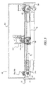
- Measurement and transport apparatus 16 is now more particularly described. This apparatus, illustrated in Figures 5-14, allows for the transport of the material at the necessary degree of flatness and speed to provide accurate measurements without data loss.
- Measurement and transport apparatus 16 includes a transport mechanism 50 for transporting a length of material M in a first direction along transport path P through a measurement zone Z adjacent optical probe 18 as shown in Figure 8.
- Transport mechanism 50 includes an open channel 52 defining the transport path P.
- Channel 52 is defined by a bottom wall 54 having a recessed web relief track 60 disposed along its length, two side walls 56,57, and two tops walls 58,59. The two top walls are spaced apart to provide an opening in the channel to allow the optical probe to be disposed adjacent the moving material M.
- This opening channel 52 having recessed web relief track 60 a portion of material M in measurement zone Z does not contact any component of the transport mechanism.
- Channel 52 has a width greater than, but substantially equal to, the width of the material so that the material does not move laterally along the sample path. For example, for a length of material M having a width of approximately 35mm, channel 52 would have a width of 35 + ⁇ 2mm. Similarly, the distance between top walls 58,59 and bottom wall 54 must be sufficient to transport the maximum web thickness of the samples being measured. For web thickness in the range of 2-10 mils, a distance of 20 mils is sufficient, particularly if the material includes knurled portions. The combination of the width dimension and the length dimension of channel 52 maintaining the material flat in the measurement region and reduces edge effects as the material enters and exits the channel.
- the length of the base support be at least 5 times the width of the material. For example, for a material having a width of approximately 35 mm, channels of 7-32 inches in length have been found suitable.
- Web relief track 60 is recessed within bottom wall 54 to provide a portion of material M which is not contacted by transport mechanism 50.
- Optional ionized air inlets 62 are positioned along web relief track 60 to prevent static build-up on material M as it is transported, as illustrated in Figure 6.
- An optional static-preventing member 64 may surround a portion of or all of measurement and transport apparatus 16 to prevent static build-up on the material.
- such a static-preventing member could be an ion-purged transparent cover which provides ionized air.
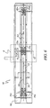
- Transport mechanism 50 also includes a stepper motor 66 (refer to Figure 7) in mechanical association with a drive roller 68 (refer to Figure 5) to transport material M through channel 52.
- Stepper motor 66 is controlled by a Programmable Logic Controller (PLC) or computer (not shown) to obtain various sample speeds.
- PLC Programmable Logic Controller
- a preferred arrangement includes a 3:1 planetary gear 70 employed in the mechanical association. This gearing arrangement allows stepper motor 66 to operate at a higher, smoother speed.
- the gearing arrangement increases the torque at drive roller 68.
- Each one of a pair of drive pinch rollers 72a,72b forms a nip with drive roller 68 wherein the material passes through the nips at a predetermined constant speed S.
- Drive pinch rollers 72a,72b are spaced apart from each other to provide a region on material M that does not contact the components of the transport so as to adversely affect the characteristics of the material.
- Drive roller 68 is in mechanical association with an inlet roller 74 disposed near inlet 12 of transport path P, and an outlet roller 76 disposed near outlet 14 of transport path P, as illustrated in Figure 5.
- rollers 68, 74 and 76 are of substantially equal diameter.
- the mechanical association can be accomplished, for example, by toothed belts B 1 ,B 2 coupled to toothed pulleys 68a, 74a, and 76a attached to roller shafts of drive 68, inlet 74, and outlet 76 rollers, respectively.
- Drive roller toothed pulley 68a (shown in Figure 7) is a dual pulley for coupling to both toothed belts B 1 and B 2 . All three rollers (drive 68, inlet 74, and outlet 76) have a recessed center portion which aids in reducing dirt buildup reduces the amount of contact with material M, and provides for a non-contact measurement region.
- a pair of inlet pinch rollers 78a,78b form nips with inlet roller 74.
- a pair of outlet pinch rollers 80a,80b form nips with outlet roller 76.
- Drive, inlet, and outlet rollers 68,74,76 are preferably comprised of anodized aluminum with a urethane coating.
- Drive pinch rollers 72a,72b are preferably comprised of a Delrin material, as is inlet and outlet nip rollers 78a,78b, 80a,80b.
- the drive pinch rollers and inlet and outlet nip rollers may include a suitable polymer such as an O-ring 81 of EDPM, as illustrated in Figure 10, to provide for non-slippage during transport.
- Inlet roller 74 operates at a speed slightly less than speed S of drive roller 68. This operation is accomplished by toothed pulley 74a coupled to drive roller dual toothed pulley 68a by means of belt B 1 . Inlet roller pulley 74a has slightly more teeth per revolution than drive roller dual toothed pulley 68a. A roller clutch 82 is coupled to inlet roller 74 to aid in uniform transport of material M. As the length of material M enters the nip formed with drive roller 68, the length is pulled from the slightly slower speed inlet roller 74 with no drag due to the free rolling clutch of roller clutch 82.
- Outlet roller 76 operates as a speed slightly greater than speed S of drive roller 68. This operation is accomplished by toothed pulley 76a coupled to drive roller dual toothed pulley 68a by means of belt B 2 . Outlet roller pulley 76a has slightly fewer teeth per revolution than drive roller dual toothed pulley 68a. Outlet pinch rollers 80a,80b are biased away from the transport path P, for example by a resilient member 85 such as a spring shown in Figure 5. As will be discussed in more detail below, at least one solenoid 86 causes outlet pinch rollers 80a,80b to overcome the biasing of resilient member 85 to form a nip with outlet roller 76 when the trailing end of the length of material M is sensed. This formation of the nip between outlet pinch rollers 80a,80b and outlet roller 76 causes a quick exit of the trailing end of the length of the material.
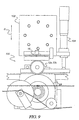
- At least one sensor is mounted in overlapping orientation to the transport path in measurement region R to detect the leading and trailing ends of the length of material M during transport. More particularly, measurement region R is located along web relief track 60, intermediate drive pinch rollers 72a,72b.
- the present invention preferably employs two sensors 90,92 mounted side-by-side on a sliding rail so as to be independently positioned, with the web measurement location disposed between the sensors.
- Figure 10 illustrates this web measurement location by a cone C of light directed toward material M from optical probe 18.
- Suitable sensors are light emitting diode photodetector reflective pair assemblies such as Honeywell HOA1160-2.
- the sensors are employed, for example, to start and stop the data acquisitions of the measurements.
- Sensors 90,92 may be slightly offset, with the sensors being positioned substantially opposing optical probe 18. This permits one sensor to detect the leading edge immediately prior to optical probe 18, with a resulting signal being used to start the measurements, and permits the other sensor to detect the trailing end immediately after optical probe 18, with a resulting signal being used to end the measurements. (One sensor may be used to detect both the leading edge and the trailing end.)
- the leading and/or the trailing end of the length of material M may include knurled areas or other distinctive markings which may not be analyzed for thickness.
- measurement and transport apparatus 50 also comprises a measurement mechanism 100 having an optical probe mounting plate 102, and a height adjusting apparatus 104, and optical probe 18. Adjusting apparatus 104 adjusts the position of optical probe mounting plate 102 relative to the transport path P, and move moves in a direction substantially perpendicular to the channel as illustrated in Figure 9 by arrow D. Optical probe 18 is affixed to optical probe mounting plate 102.
- optical probe 18 is more particularly illustrated in Figures 11-14.
- optical probe 18 preferably includes a gimbal mount having a ball pivot point 108.
- Optical probe 18 is affixed to optical probe mounting plate 102 by a plurality of mechanical fasteners (not shown) and includes a fiber mount 112 such as a Rifocs Part No. DAK-13/FC.
- fiber mount 112 such as a Rifocs Part No. DAK-13/FC.
- Adjusting members 110 provide adjustment to align optical probe 18 normal to channel 52 so as to be normal to the surface of material M as it moves along the transport path.
- Optical probe 18 is the interface between interferometer apparatus 20 and the length of material being measured.
- Optical probe 18 preferably includes a GRIN lens.
- the positioning of optical probe 18 relative to the channel is dependent on the focal length of the optical probe.
- the focal length of the lens is strongly dependent on the lens to optical fiber spacing.
- a 3mm diameter, 0.11 pitch NSG America (SLW 300011 130NCO) for 1300nm operation with an approximate 28.5 mm focal length was utilized, a depth of focus of 2.5 mm and a focused beam spot size of 47 ⁇ m.
- the lens-to-fiber spacing is 4.7 mm.
- the light through the optical fiber must be centered on the GRIN lens axis. Accordingly, the lens must be properly aligned for accurate measurements.
- material M is transported along the transport path P through channel 52 to enter the nip formed by inlet roller 74 and inlet pinch rollers 78a,78b.
- one of sensors 90,92 senses the leading edge of the material, and the sensor provides a signal to initiate the acquiring of data.
- optical probe 18 directs a beam of light toward a segment of the moving material.
- Interferometer apparatus 20 collects a portion of the light reflected from the optical interfaces of the segment of material M, and generates an interference signal representative of the collected light.
- the sensor When the other of sensors 90,92 senses the trailing end of the length within the measurement region R, the sensor provides a signal to stop the acquisition of data.
- solenoid 86 is activated to overcome the biasing of resilient member 85 and form a nip between outlet roller 76 and outlet nip rollers 80a,80b, causing the trailing end to quickly exit the channel.
- the data values acquired by data acquisition module 22 are converted to thickness values by analyzer 24 to provide a thickness profile of the material in the direction of movement.
- interferometer apparatus 20 is initialized for operation. Predetermined values are selected for a motor amplitude and offset so as to identify triplet peak formations, as shown in absolute value representation in Figure 16. Large amplitude peaks, (e.g., peaks 2, 5, 8, and 11) illustrated in Figure 16 are referred to as zero-crossing peaks. A set of smaller peaks are adjacent to each zero-crossing peak (e.g., peaks 1, 3, 4, 6, 7 and 8). The distance between the large and small peaks (e.g., distance from 1-2, 2-3, and 4-5 of Figure 16) are indicative of the optical path (nt).
- the interferometer motor amplitude and motor start position are selected such that the optical path (nt) is less than the intervals between adjacent small peaks (e.g., 3-4, 6-7, 9-10 in Figure 16).
- a single interferometer motor scan would include three peaks having a small, large, and small amplitude.
- the interferometer motor scanning direction would change between peaks 3-4, 6-7, 9-10, etc, as shown in Figure 16.
- the intervals between adjacent small peaks can be made to be consistently smaller than the optical path (nt).
- Appropriate gain levels are selected so as to not saturate amplifiers when zero-crossing peaks are present.
- the set of adjacent small interference peak amplitudes must also be large enough to exceed a required threshold value.
- predetermined values can be selected for a motor amplitude and offset so as to identify doublet peak formations.
- data is collected at constant distance intervals using an A-D converter.
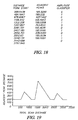
- the data represented in Figure 16 shows the absolute value of the A-D converter counts (vertical axis) versus the accumulated interferometer motor scan distance (horizontal axis).
- the measurements are performed at a relatively constant interferometer motor scan frequency, for example at 10 Hz.
- the speed of material M through a measurement zone (defined as an area in the channel about the optical probe) is predetermined and is substantially constant for ease of calculations.
- a measurement time interval from start to stop trigger signals i.e., the detection of the leading edge and the trailing end by sensors 90,92
- sensors 90,92 are disposed at the substantially same relative position within channel 52 as optical probe 18. Offsetting their positions would be accommodated by incorporating a constant and predetermined delay.
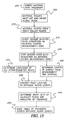
- interferometer apparatus 20 With interferometer apparatus 20 initialized for operation, the following steps are conducted to provide a thickness profile.
- the leading edge of the length of material M is inserted into inlet 12 of the transport path P so as to be disposed within channel 52 (step 200 illustrated in Figure 15).
- the length of material M is automatically transported through the channel (step 205) of Figure 15).
- the leading edge enters the drive pinch roller area (step 210)
- the leading edge is detected by sensor 90, and a signal is sent to interferometer apparatus 20 to initiate collection of interferometer data at constant distance intervals (step 215 of Figure 15). Accordingly, digital signal amplitude data is sent and stored in a sequential data file, and the time at which the leading edge is detected is stored.
- the collection of interferometer data is stopped, and digital signal amplitude data is no longer sent and stored in the sequential data file (step 220 of Figure 15).
- the time at which the trailing end is detected is also stored.
- Figure 17 illustrates a subset of the peaks shown in Figure 16.
- the first column of the data table shows, for each peak, a calculated distance D j from the origin of all the calculated peaks (step 235 of Figure 15).
- the last row of the data tables shows the distance D q from the origin of the last data point which corresponds to the trailing end of the material.
- a pattern recognition classifier is used to assist in the determination of which sets of adjacent peaks should be utilized in a thickness profile determination (step 240 of Figure 15).
- the small amplitude and large amplitude zero-crossing peaks can be thought of as binary signals of level 0 (small) and 1 (large).
- the third data column of Figure 18 shows the amplitude classifier level for each of the peaks shown in Figure 17.
- optical path length indicating peaks are due to a pair of adjacent peaks of amplitude classifier levels 0-1 or 1-0.
- the sets of adjacent peaks which fulfill this criteria are peak sets 1-2, 2-3, 4-5, 5-6, 7-8, 8-9, 10-11, and 11-12.
- the usual sequence of adjacent amplitude peaks of 010010010010 occurs.
- the 010010 pattern can be construed as a pattern recognition classifier, indicating no loss of data. With some materials, it is possible that a double reflection could occur at twice the optical path. This would result in an adjacent peak pattern of 0010000100 for the classifiers. This pattern can be construed as a pattern recognition classifier for a double reflection. Only the adjacent peaks with amplitudes 0-1 and 1-0 would be used in the optical path measurement calculations. In some cases there may be lost data due to peaks not having enough amplitude. In this case, adjacent peak amplitude patterns such as 0101010010 may occur. To accommodate for this case, a thickness range acceptance criteria is devised in addition to the amplitude classifier selection criteria.
- Figure 17 of US Patent No. 5,659,392 ( Marcus et al ) and 5,596,409 ( Marcus et al ) illustrate an example of doublet peak formation in absolute value representation.
- the pattern recognition classifier for doublet peak formation without loss of data is 011001100 or 10011001100.
- the peaks and locations are selected that meet both the classifier amplitude criteria and thickness range acceptance criteria for potential optical path indicative sets of peaks.
- the peaks that fit the acceptance criteria are stored in a subarray T i with their corresponding distances from the origin (step 245 of Figure 15).
- An example of an acceptance criteria is: product aim ⁇ 25 um.
- 195 ⁇ 25 may be used as the acceptance criteria.
- Figures 20-21 shows the processed data set for the data of Figures 17-18.
- the first column of data in Figure 20 shows the selected peaks distances from the origin.
- the second column of Figure 20 shows an optional adjusted distances D j ' for the selected peaks.
- the adjusted distance calculation takes into account that the material is moving during the measurement. The average position of the material during a measurement is midway between the two adjacent peaks used in its optical path length calculation. For long lengths of material with many data points, the adjusted distance calculation is a minor correction and is not necessary.
- the third column of Figure 20 shows the calculated locations of the measured points along the material length.
- the optional adjusted distances D j ' for the selected peaks are calculated as follows.
- the optical path is equal to the distance between two adjacent peaks, thus the average location of the material during the measurement is at a distance halfway between the two peaks.
- the measurement interval is divided into scanning intervals S 1 and S 2 as shown Figure 17. With general measurement conditions, typically 4 measurements occur over the distance range S 1 + S 2 . Markers can be included to the data array to monitor lost data locations. This is used to prevent averaging over lost data regions, and is further discussed below with reference to Figure 22.
- Figure 22 shows the post processing method to present a thickness profile once the table of thickness verses distance along the length is obtained (step 245 of Figure 15).
- an outlier as being a location wherein there is no thickness data or a location of a peak which does not meet the thickness acceptance range, and is out of the reasonable range of thickness based on the standard deviation of the data set. Accordingly, these outliers are searched for and marked (i.e., noted or flagged), for example, as having a zero value. As such, during the moving average calculation, the marked outliers are excluded from the average.
- outliers are searched for, and marked as having a zero value (step 255).
- the data may be averaged over several adjacent thickness measurements (step 260). For example, the data could be averaged over every 3-to-35 adjacent thickness measurements, excluding the zero marked outliers.
- the thickness at location m would become the average of locations m-1, m, and m+1. If location m+1 is an outlier, then the moving average will be an average of only locations m-1 and m.
- the selected averaging may depend on the number of measurements acquired.
- step 265 it may be desired to exclude the data collected at the leading edge and trailing end of the material (step 265), for example, if the ends are knurled (i.e., areas of raised ridges/bumps).
- the number of measurements acquired is compared to the determined length of the material (step 230 of Figure 15) to determine if an acceptable minimum number of data points has been obtained (step 270). For example, an acceptable minimum number could be 95 percent. If not, an error message is provided (step 275) and further calculations are not made (step 295). If an acceptable minimum is obtained, the distance scale is adjusted (step 280) and the thickness profile is displayed (step 290).
- Further information about the measurement may be displayed. For example, it may be desirable to visually display the location and magnitude of the three highest local slopes on the thickness profile.
- Various other material statistics may be desired, for example, average thickness, standard deviation, and maximum and minimum deviation from a desired aim thickness along with their locations.
- Applicants have found the present invention suitable for lengths of material up to 200 feet (60 m). Cutting of material M may be advantageous in particular applications, particularly if a supply of web material is being measured. Therefore, a cutting mechanism (not shown) may be optionally disposed along the transport path, prior to the inlet of the channel. This cutting mechanism would allow for various lengths of material to be measured from the supply.
Description
- The present invention relates generally to the measurement of physical properties of a moving object by non-contact optical interferometry. More particularly, the invention concerns an apparatus and method for providing material thickness profiles of a moving length of material such as film, sheet, or web.
- In many industrial processes, control of material thickness is of critical importance, particularly during the manufacturing of layered or coated web material. For example, the manufacturing of photographic film requires the formation of a uniform layer of emulsion on a base support. Non-contact thickness measuring means are preferred so as to not adversely affect the characteristics of the material and to minimize dust, dirt or film residue buildup in a sensor head of a measurement apparatus. Residue buildup on a measurement sensor head would adversely affect the measurement resolution and could result in the loss of data.
- Methods for measuring the thickness of a material using interferometers are known in the prior art. For example, US Patent No. 3,319,515 (Flournoy) relates to the determination of thickness on the basis of interferometric optical phase discrimination. US Patent No. 5,473,432 (Sorin) and US Patent No. 5,610,716 (Sorin et al) relate to an apparatus and method for measuring film thickness of a moving film, employing optical reflectrometry. Factors of a moving material, such as vibrations, lateral movements, flutter coupled with angular variation, standing waves, and fluctuations, would render the thickness measurements inaccurate and unintelligible or result in a loss of data. Sorin attempts to account for flutter through the incorporation of an adjustable numerical aperture lens. However, in situations of high flutter, continuous adjustment of the numerical aperture lens is impractical. As the numerical aperture is decreased to tolerate additional flutter, the acceptance angle for reflected light going back into the fiber decreases.
- Non-contact thickness measurement methods based on beta, Rutherford backscattering or gamma rays are known to the prior art. These non-contact methods require relatively large beam spot sizes (e.g., one-half inch diameter or larger) to acquire a measurement with sufficient signal-to-noise ratio to provide a useful thickness measurement profile.
- Accordingly, a need continues to exist for an apparatus and method for measuring the thickness of a moving material without adversely affecting the material. A need also exists to measure materials with a high degree of lateral resolution. In situations wherein some loss of data may occur, a need further exists to account for the lost data, and to provide a meaningful thickness profile.
- An object of the present invention is to provide an improved apparatus and method for measuring the thickness of a moving material.
- A further object of the present invention is to provide such an apparatus and method to provide a thickness profile of the material in the direction of the movement of the material.
- Still another object of the present invention is to provide such an apparatus and method which provides accurate and reliable measurements with minimum loss of thickness information and provides a meaningful thickness profile.
- Yet another object of the present invention is to provide such an apparatus and method which provides measurements with a high degree of lateral resolution.
- These objects are given only by way of illustrative example. Thus, other desirable objectives and advantages inherently achieved by the disclosed invention may occur or become apparent to those skilled in the art. The invention is defined by the appended claims.
- According to the invention, there is provided a method for determining a thickness of a moving material having at least two optical interfaces. The method includes the steps of transporting a length of material along a transport path through a measurement region; maintaining a substantially constant velocity of the moving length through the measurement region; maintaining a predetermined flatness to the moving length through the measurement region; directing a beam of light toward a segment of the moving length disposed within the measurement region; collecting a portion of the light reflected from the optical interfaces of the segment of the moving length; directing the collected light toward an interferometer apparatus; generating an interference signal representative of the collected light; and analyzing the interference signal to determine a thickness profile of the material in the first direction.
- The present invention provides an improved method for providing material thickness profiles of a moving length of material, such as film, sheet, or web. Factors of the moving web are taken into account to provide accurate measurements with minimum loss of thickness. Non-contact measuring means are employed, thereby not adversely affecting the measurements or the characteristics of the material. The present invention can be employed for quality control purposes of the manufacturing equipment or for certification procedures whereby a standard sample can be measured multiple times to test and compare manufacturing equipment performance.
- The foregoing and other objects, features, and advantages of the invention will be apparent from the following more particular description of the preferred embodiments of the invention, as illustrated in the accompanying drawings.
- FIG. 1 shows a measurement system for measuring material thickness profiles in accordance with the present invention.
- FIG. 2 shows an example of a material thickness profile of a length of material provided by the measurement system of FIG. 1.
- FIG. 3 shows a length of material illustrating the orientation of the material for lengthwise and widthwise thickness profile measurements.
- FIG. 4 shows an interferometer apparatus suitable for use with the measurement system of FIG. 1.
- FIG. 5 shows a front view of a transport and measurement apparatus in accordance with the present invention.
- FIG. 6 shows a top view of the transport and measurement apparatus of FIG. 5.
- FIG. 7 shows a side view of the transport and measurement apparatus of FIG. 5.
- FIG. 8 shows an enlarged partial side view of the channel of the transport and measurement apparatus.
- FIG. 9 shows and enlarged view of the drive roller and the optical mounting plate of FIG. 5.
- FIG. 10 shows a partial side view of the drive roller and the drive pinch rollers.
- FIGS. 11-14 show an illustrative view, side views, and a top view of the optical probe mount in accordance with the present invention.
- FIG. 15 shows a flow chart generally illustrating the operational method in accordance with the present invention.
- FIG. 16 generally shows a triplet peak formation in absolute value representation.
- FIG. 17 shows generally shows a portion of the peak formations of FIG. 16.
- FIG. 18 shows a tabular format showing the distances between the peaks illustrated in FIG. 16.
- FIG. 19 shows a graph of the table data of FIG. 18.
- FIG. 20 shows a tabular format showing the distances for the peaks of FIG. 16 after applying a pattern recognition classifier.
- FIG. 21 shows a graph of the table data of FIG. 20.
- FIG. 22 shows a post processing method in accordance with the present invention.
-
- The following is a detailed description of the preferred embodiments of the invention, reference being made to the drawings in which the same reference numerals identify the same elements of structure in each of the several figures.
- Figure 1 generally illustrates a measurement system 10 in accordance with the present invention suitable to determine a thickness profile of a moving material having a predetermined width. A length of material M is transported along a transport path P from an inlet 12 to an outlet 14 in a direction indicated by arrow A. The length of material M has a leading and trailing end. As shown in Figure 1, disposed in the transport path P is a measurement and transport apparatus 16, which is more particularly described below. As illustrated in Figure 1, disposed adjacent measurement and transport apparatus 16 is an optical probe 18 arranged in an appropriate orientation with material M to enable the measurement of the thickness profile of material M. This orientation will be further discussed below.
- As the material is transported, optical probe 18 directs a beam of light through single mode optical fiber 19 toward a segment of the moving material. An interferometer apparatus 20 collects a portion of the light reflected from the optical interfaces of the segment of material M, and generates an interference signal representative of the collected light. The interference signals are provided to a photodetector internal to interferometer apparatus 20 and converted to an analog electrical signal. The analog electrical signal is amplified and filtered and then converted to digital data by an A-D converter in a data acquisition module 22. The digital data is then converted to thickness values by an analyzer 24. Optionally, data acquisition module 22 and analyzer 24 may be incorporated into a computer 25, as illustrated in Figure 1. An ordered array of the thickness values provides a thickness profile of the material in the direction of movement. Figure 2 shows an example of a thickness profile (y-axis) for a 54 inch length of the material (x-axis).
- Material M may be in sheet or web form and can be comprised of single or multiple layers. For ease of discussion, material M will be assumed to be comprised of a single layer having two optical interfaces: a front surface F and a back surface B. Further, material M can be transparent, colored, or partially opaque (i.e., an optical density less than 4 at the measured wavelength). Figure 3 illustrates a length of material M having a length L and a width W. The thickness profile illustrated in Figure 2 can be a lengthwise thickness profile (i.e., the x-axis of Figure 2 has a range of the value of length L), or a widthwise thickness profile (i.e., the x-axis of Figure 2 has a range of the value of width W). For a widthwise thickness profile, those skilled in the art will recognize that it may be preferable to slit the length of material M into a strip of substantially constant width W. For example, as illustrated in Figure 3, strip M' is slit from material M, and strip M' would be used for the widthwise thickness profile measurement. (Material M" being the remaining portion of material M after strip M' is removed.)
- A suitable interferometer apparatus 20 for use with measurement system 10 is disclosed in US Patent No. 5,659,392 (Marcus et al) and 5,596,409 (Marcus et al), which describes an apparatus and method for measuring a thickness of a material. Interferometer apparatus 20 is preferably a dual interferometer apparatus of a Michelson configuration in an autocorrelation mode, as shown in Figure 4. Optical probe 18 directs a beam of light from a non-coherent light source 30 (such as light-emitting diode (LED) toward a segment of the moving length of material M. Optical probe 18 includes a Gradient Index lens (e.g., GRIN). The light is reflected on the front F and back B surfaces of material M and the light signals are introduced into two arms of interferometer apparatus 20 through a 1x2 optical coupler 32 and a fiber collimator 34. A coherent light source 36 (such as a HeNe laser) emits a beam of light toward a beam splitter 38. Beam splitter 38 divides the beams of light into pairs of light beams directed toward a pair of hollow-cube retroreflectors 40,42 which are mounted 90 degrees apart and move in perpendicular directions as shown by arrows B and C. The outputs of interferometer apparatus 20 are directed to a pair of detectors 44,46 for LED 30 and laser 36, respectively. The non-coherent light of LED 30 follows the same light path as the coherent light path of HeNe laser 36, but in reverse time order. A band-pass filter 48 blocks the light from laser 36 being incident on material M. A second filter 50 prevents light from LED 30 from interfering with the light from laser 36.
- As such, the laser interferometer tracks the distance the optical path has changed, with the laser signal providing data acquisition trigger signals, at constant distance intervals, for collecting interferometric data from the LED interferometer. Therefore, the purpose of the laser interferometer is to track the distance the optical path moves while the LED interferometer is collecting data from material M.
- Applicants have discovered that a particular degree of flatness of material M must be maintained when the material moves past optical probe 18. If the flatness is not maintained, aberrations such as vibrations, lateral movements, standing waves, and fluctuations render thickness measurements inaccurate and unintelligible. Accordingly, Applicants have devised a measurement and transport apparatus 16 to maintain material M to a predetermined flatness. Applicants have determined that, for a particular lens, material M must be flat to within one degree (1°) of normal from the transport path within the measurement region. More particularly, Applicants have determined that optical probe 18 provides for a one degree variation from normal with a 2mm depth of focus.
- Measurement and transport apparatus 16 is now more particularly described. This apparatus, illustrated in Figures 5-14, allows for the transport of the material at the necessary degree of flatness and speed to provide accurate measurements without data loss.
- Measurement and transport apparatus 16 includes a transport mechanism 50 for transporting a length of material M in a first direction along transport path P through a measurement zone Z adjacent optical probe 18 as shown in Figure 8. Transport mechanism 50 includes an open channel 52 defining the transport path P. Channel 52 is defined by a bottom wall 54 having a recessed web relief track 60 disposed along its length, two side walls 56,57, and two tops walls 58,59. The two top walls are spaced apart to provide an opening in the channel to allow the optical probe to be disposed adjacent the moving material M. By this opening channel 52 having recessed web relief track 60, a portion of material M in measurement zone Z does not contact any component of the transport mechanism.
- Channel 52 has a width greater than, but substantially equal to, the width of the material so that the material does not move laterally along the sample path. For example, for a length of material M having a width of approximately 35mm, channel 52 would have a width of 35 + ∼ 2mm. Similarly, the distance between top walls 58,59 and bottom wall 54 must be sufficient to transport the maximum web thickness of the samples being measured. For web thickness in the range of 2-10 mils, a distance of 20 mils is sufficient, particularly if the material includes knurled portions. The combination of the width dimension and the length dimension of channel 52 maintaining the material flat in the measurement region and reduces edge effects as the material enters and exits the channel. Applicants have discovered that a sufficiently long channel is advantageous to maintaining the material flat, and accordingly, prefer that the length of the base support be at least 5 times the width of the material. For example, for a material having a width of approximately 35 mm, channels of 7-32 inches in length have been found suitable.
- Web relief track 60 is recessed within bottom wall 54 to provide a portion of material M which is not contacted by transport mechanism 50. Optional ionized air inlets 62 are positioned along web relief track 60 to prevent static build-up on material M as it is transported, as illustrated in Figure 6. An optional static-preventing member 64 may surround a portion of or all of measurement and transport apparatus 16 to prevent static build-up on the material. For example, such a static-preventing member could be an ion-purged transparent cover which provides ionized air.
- Transport mechanism 50 also includes a stepper motor 66 (refer to Figure 7) in mechanical association with a drive roller 68 (refer to Figure 5) to transport material M through channel 52. Stepper motor 66 is controlled by a Programmable Logic Controller (PLC) or computer (not shown) to obtain various sample speeds. A preferred arrangement includes a 3:1 planetary gear 70 employed in the mechanical association. This gearing arrangement allows stepper motor 66 to operate at a higher, smoother speed. In addition, the gearing arrangement increases the torque at drive roller 68. Each one of a pair of drive pinch rollers 72a,72b (refer to Figure 6) forms a nip with drive roller 68 wherein the material passes through the nips at a predetermined constant speed S. Drive pinch rollers 72a,72b are spaced apart from each other to provide a region on material M that does not contact the components of the transport so as to adversely affect the characteristics of the material.
- Drive roller 68 is in mechanical association with an inlet roller 74 disposed near inlet 12 of transport path P, and an outlet roller 76 disposed near outlet 14 of transport path P, as illustrated in Figure 5. For ease of discussion, rollers 68, 74 and 76 are of substantially equal diameter. The mechanical association can be accomplished, for example, by toothed belts B1,B2 coupled to toothed pulleys 68a, 74a, and 76a attached to roller shafts of drive 68, inlet 74, and outlet 76 rollers, respectively. Drive roller toothed pulley 68a (shown in Figure 7) is a dual pulley for coupling to both toothed belts B1 and B2. All three rollers (drive 68, inlet 74, and outlet 76) have a recessed center portion which aids in reducing dirt buildup reduces the amount of contact with material M, and provides for a non-contact measurement region.
- A pair of inlet pinch rollers 78a,78b form nips with inlet roller 74. Similarly, a pair of outlet pinch rollers 80a,80b form nips with outlet roller 76. Drive, inlet, and outlet rollers 68,74,76 are preferably comprised of anodized aluminum with a urethane coating. Drive pinch rollers 72a,72b are preferably comprised of a Delrin material, as is inlet and outlet nip rollers 78a,78b, 80a,80b. The drive pinch rollers and inlet and outlet nip rollers may include a suitable polymer such as an O-ring 81 of EDPM, as illustrated in Figure 10, to provide for non-slippage during transport.
- Inlet roller 74 operates at a speed slightly less than speed S of drive roller 68. This operation is accomplished by toothed pulley 74a coupled to drive roller dual toothed pulley 68a by means of belt B1. Inlet roller pulley 74a has slightly more teeth per revolution than drive roller dual toothed pulley 68a. A roller clutch 82 is coupled to inlet roller 74 to aid in uniform transport of material M. As the length of material M enters the nip formed with drive roller 68, the length is pulled from the slightly slower speed inlet roller 74 with no drag due to the free rolling clutch of roller clutch 82.
- Outlet roller 76 operates as a speed slightly greater than speed S of drive roller 68. This operation is accomplished by toothed pulley 76a coupled to drive roller dual toothed pulley 68a by means of belt B2. Outlet roller pulley 76a has slightly fewer teeth per revolution than drive roller dual toothed pulley 68a. Outlet pinch rollers 80a,80b are biased away from the transport path P, for example by a resilient member 85 such as a spring shown in Figure 5. As will be discussed in more detail below, at least one solenoid 86 causes outlet pinch rollers 80a,80b to overcome the biasing of resilient member 85 to form a nip with outlet roller 76 when the trailing end of the length of material M is sensed. This formation of the nip between outlet pinch rollers 80a,80b and outlet roller 76 causes a quick exit of the trailing end of the length of the material.
- When material M is transported through channel 52, the speed of the material is maintained at a substantially constant velocity in the area about drive roller 68. While Applicants have successfully employed the present invention for speeds from 1-10 inches/second (2-26 cm/sec), higher and lower speeds can be accommodated using the apparatus and method of the present invention.
- At least one sensor is mounted in overlapping orientation to the transport path in measurement region R to detect the leading and trailing ends of the length of material M during transport. More particularly, measurement region R is located along web relief track 60, intermediate drive pinch rollers 72a,72b. As shown in Figure 10, the present invention preferably employs two sensors 90,92 mounted side-by-side on a sliding rail so as to be independently positioned, with the web measurement location disposed between the sensors. Figure 10 illustrates this web measurement location by a cone C of light directed toward material M from optical probe 18. Suitable sensors are light emitting diode photodetector reflective pair assemblies such as Honeywell HOA1160-2. By detecting the leading and trailing end of the length of material M, the sensors are employed, for example, to start and stop the data acquisitions of the measurements. Sensors 90,92 may be slightly offset, with the sensors being positioned substantially opposing optical probe 18. This permits one sensor to detect the leading edge immediately prior to optical probe 18, with a resulting signal being used to start the measurements, and permits the other sensor to detect the trailing end immediately after optical probe 18, with a resulting signal being used to end the measurements. (One sensor may be used to detect both the leading edge and the trailing end.) Note that the leading and/or the trailing end of the length of material M may include knurled areas or other distinctive markings which may not be analyzed for thickness.
- As shown in Figure 9, measurement and transport apparatus 50 also comprises a measurement mechanism 100 having an optical probe mounting plate 102, and a height adjusting apparatus 104, and optical probe 18. Adjusting apparatus 104 adjusts the position of optical probe mounting plate 102 relative to the transport path P, and move moves in a direction substantially perpendicular to the channel as illustrated in Figure 9 by arrow D. Optical probe 18 is affixed to optical probe mounting plate 102.
- Optical probe 18 is more particularly illustrated in Figures 11-14. As illustrated, optical probe 18 preferably includes a gimbal mount having a ball pivot point 108. Optical probe 18 is affixed to optical probe mounting plate 102 by a plurality of mechanical fasteners (not shown) and includes a fiber mount 112 such as a Rifocs Part No. DAK-13/FC. When optical probe 18 is affixed, it is positioned in overlapping relation to web relief track 60 of the transport path P over drive roller 68, and over sensors 90,92 (refer to Figure 10). Adjusting members 110 provide adjustment to align optical probe 18 normal to channel 52 so as to be normal to the surface of material M as it moves along the transport path. Optical probe 18 is the interface between interferometer apparatus 20 and the length of material being measured.
- Optical probe 18 preferably includes a GRIN lens. The positioning of optical probe 18 relative to the channel is dependent on the focal length of the optical probe. For example, in a GRIN lens, the focal length of the lens is strongly dependent on the lens to optical fiber spacing. For Applicant's particular application, a 3mm diameter, 0.11 pitch NSG America (SLW 300011 130NCO) for 1300nm operation with an approximate 28.5 mm focal length was utilized, a depth of focus of 2.5 mm and a focused beam spot size of 47 µm. The lens-to-fiber spacing is 4.7 mm. For the light to be normal to the axis of the GRIN lens, the light through the optical fiber must be centered on the GRIN lens axis. Accordingly, the lens must be properly aligned for accurate measurements.
- In operation, once optical probe 18 is properly aligned, material M is transported along the transport path P through channel 52 to enter the nip formed by inlet roller 74 and inlet pinch rollers 78a,78b. As material M enters measurement region R and the nip formed by drive roller 68 and drive pinch rollers 72a,72b, one of sensors 90,92 senses the leading edge of the material, and the sensor provides a signal to initiate the acquiring of data. As the length of material M is transported past optical probe 18, optical probe 18 directs a beam of light toward a segment of the moving material. Interferometer apparatus 20 collects a portion of the light reflected from the optical interfaces of the segment of material M, and generates an interference signal representative of the collected light. When the other of sensors 90,92 senses the trailing end of the length within the measurement region R, the sensor provides a signal to stop the acquisition of data. In addition, solenoid 86 is activated to overcome the biasing of resilient member 85 and form a nip between outlet roller 76 and outlet nip rollers 80a,80b, causing the trailing end to quickly exit the channel. The data values acquired by data acquisition module 22 are converted to thickness values by analyzer 24 to provide a thickness profile of the material in the direction of movement.
- The measurement technique is now more particularly described with reference to Figures 15-22. After optical probe 18 is properly mounted and aligned, interferometer apparatus 20 is initialized for operation. Predetermined values are selected for a motor amplitude and offset so as to identify triplet peak formations, as shown in absolute value representation in Figure 16. Large amplitude peaks, (e.g., peaks 2, 5, 8, and 11) illustrated in Figure 16 are referred to as zero-crossing peaks. A set of smaller peaks are adjacent to each zero-crossing peak (e.g., peaks 1, 3, 4, 6, 7 and 8). The distance between the large and small peaks (e.g., distance from 1-2, 2-3, and 4-5 of Figure 16) are indicative of the optical path (nt). Accordingly, the interferometer motor amplitude and motor start position (offset) are selected such that the optical path (nt) is less than the intervals between adjacent small peaks (e.g., 3-4, 6-7, 9-10 in Figure 16). In the present instance, a single interferometer motor scan would include three peaks having a small, large, and small amplitude. The interferometer motor scanning direction would change between peaks 3-4, 6-7, 9-10, etc, as shown in Figure 16. Alternatively, the intervals between adjacent small peaks can be made to be consistently smaller than the optical path (nt). Appropriate gain levels are selected so as to not saturate amplifiers when zero-crossing peaks are present. The set of adjacent small interference peak amplitudes must also be large enough to exceed a required threshold value.
- While not shown, note that as an alternative to triplet peak formations, predetermined values can be selected for a motor amplitude and offset so as to identify doublet peak formations.
- By using the laser interferometer to trigger data acquisition of the non-coherent light interferometer, data is collected at constant distance intervals using an A-D converter. For ease of illustration, the data represented in Figure 16 shows the absolute value of the A-D converter counts (vertical axis) versus the accumulated interferometer motor scan distance (horizontal axis).
- The measurements are performed at a relatively constant interferometer motor scan frequency, for example at 10 Hz. In addition, the speed of material M through a measurement zone (defined as an area in the channel about the optical probe) is predetermined and is substantially constant for ease of calculations. Further, a measurement time interval from start to stop trigger signals (i.e., the detection of the leading edge and the trailing end by sensors 90,92) can be used to determine the length of the length of material M. For ease of discussion, sensors 90,92 are disposed at the substantially same relative position within channel 52 as optical probe 18. Offsetting their positions would be accommodated by incorporating a constant and predetermined delay.
- With interferometer apparatus 20 initialized for operation, the following steps are conducted to provide a thickness profile. The leading edge of the length of material M is inserted into inlet 12 of the transport path P so as to be disposed within channel 52 (step 200 illustrated in Figure 15). Once the leading edge is inserted through the nip formed by inlet roller 82 and inlet pinch rollers 78a,78b, the length of material M is automatically transported through the channel (step 205) of Figure 15). When the leading edge enters the drive pinch roller area (step 210), the leading edge is detected by sensor 90, and a signal is sent to interferometer apparatus 20 to initiate collection of interferometer data at constant distance intervals (step 215 of Figure 15). Accordingly, digital signal amplitude data is sent and stored in a sequential data file, and the time at which the leading edge is detected is stored.
- When the trailing end of the length of material M is detected by sensor 92, the collection of interferometer data is stopped, and digital signal amplitude data is no longer sent and stored in the sequential data file (step 220 of Figure 15). The time at which the trailing end is detected is also stored. For ease of discussion, a total number of data points is identified as q, with a data point index ranging from N = 1 to q. Further, the first data point is defined as the origin; and the measurement distance interval between adjacent interferometer sampled data points is defined as δx. Consequently, the scan distance dj from the origin to the Nth data point for j = 1 to q is given by:
- Similarly, the total scan distance dq is given by:
- A first data point N = 1 corresponds to the leading edge of the length of material M, and a last data point N = q corresponds to the trailing end.
- A length L of the length of material M is calculated (step 230 of Figure 15) using the time interval between the detection of the leading edge and trailing end by sensors 90,92 (tT) and the predetermined transport speed (VT). This length is given by:
- An algorithm is used to process the sequential data file to determine the location(s) of all the peak positions P together with their amplitudes and distances from the first data point of the data file (step 225 of Figure 15). Suitable algorithms are disclosed in US Patent No. 5,659,392 (Marcus et al) and 5,596,409 (Marcus et al), commonly assigned and incorporated herein by reference. An array of distances Dj from the origin of the interference peaks for j = 1 to P is then generated.
- Figure 17 illustrates a subset of the peaks shown in Figure 16. Referring to Figure 18, the first column of the data table shows, for each peak, a calculated distance Dj from the origin of all the calculated peaks (step 235 of Figure 15). The last row of the data tables shows the distance Dq from the origin of the last data point which corresponds to the trailing end of the material.
- The distances between all the pairs of adjacent peaks are then calculated. Referring to Figure 18, the second column shows the adjacent distances for the peaks illustrated in Figure 17. This data is also illustrated in graph form in Figure 18.
- A pattern recognition classifier, defined below, is used to assist in the determination of which sets of adjacent peaks should be utilized in a thickness profile determination (step 240 of Figure 15). The small amplitude and large amplitude zero-crossing peaks can be thought of as binary signals of level 0 (small) and 1 (large). The third data column of Figure 18 shows the amplitude classifier level for each of the peaks shown in Figure 17. Applicants note that optical path length indicating peaks are due to a pair of adjacent peaks of amplitude classifier levels 0-1 or 1-0. Referring to Figure 18, the sets of adjacent peaks which fulfill this criteria are peak sets 1-2, 2-3, 4-5, 5-6, 7-8, 8-9, 10-11, and 11-12.
- When all the peaks are present (i.e., no loss of data) the usual sequence of adjacent amplitude peaks of 010010010010 occurs. The 010010 pattern can be construed as a pattern recognition classifier, indicating no loss of data. With some materials, it is possible that a double reflection could occur at twice the optical path. This would result in an adjacent peak pattern of 0010000100 for the classifiers. This pattern can be construed as a pattern recognition classifier for a double reflection. Only the adjacent peaks with amplitudes 0-1 and 1-0 would be used in the optical path measurement calculations. In some cases there may be lost data due to peaks not having enough amplitude. In this case, adjacent peak amplitude patterns such as 0101010010 may occur. To accommodate for this case, a thickness range acceptance criteria is devised in addition to the amplitude classifier selection criteria.
- Figure 17 of US Patent No. 5,659,392 (Marcus et al) and 5,596,409 (Marcus et al) illustrate an example of doublet peak formation in absolute value representation. The pattern recognition classifier for doublet peak formation without loss of data is 011001100 or 10011001100.
- From the adjacent distance data, the peaks and locations are selected that meet both the classifier amplitude criteria and thickness range acceptance criteria for potential optical path indicative sets of peaks. The peaks that fit the acceptance criteria are stored in a subarray Ti with their corresponding distances from the origin (step 245 of Figure 15). (An example of an acceptance criteria is: product aim ± 25 um.) For the example of Figures 17-18, 195 ± 25 may be used as the acceptance criteria.
- Figures 20-21 shows the processed data set for the data of Figures 17-18. The first column of data in Figure 20 shows the selected peaks distances from the origin. The second column of Figure 20 shows an optional adjusted distances Dj' for the selected peaks. The adjusted distance calculation takes into account that the material is moving during the measurement. The average position of the material during a measurement is midway between the two adjacent peaks used in its optical path length calculation. For long lengths of material with many data points, the adjusted distance calculation is a minor correction and is not necessary. The third column of Figure 20 shows the calculated locations of the measured points along the material length.
- Note that the optional adjusted distances Dj' for the selected peaks are calculated as follows. The optical path is equal to the distance between two adjacent peaks, thus the average location of the material during the measurement is at a distance halfway between the two peaks. The adjusted distance from the origin Dj' of the jth thickness peak Tj' is given by
- The length L of material M per interferometer measurement distance interval (j = 1 - q) is given by L/dq.
- The location along the length of the material of the jth thickness peak Wj is given by:
- In some situations during a measurement, not all of the expected interferometer peaks may be observed, for example, due to scratches and excessive dirt on the material. To monitor "lost" peaks in a particular measurement, the measurement interval is divided into scanning intervals S1 and S2 as shown Figure 17. With general measurement conditions, typically 4 measurements occur over the distance range S1 + S2. Markers can be included to the data array to monitor lost data locations. This is used to prevent averaging over lost data regions, and is further discussed below with reference to Figure 22.
- Figure 22 shows the post processing method to present a thickness profile once the table of thickness verses distance along the length is obtained (step 245 of Figure 15). Applicants define an outlier as being a location wherein there is no thickness data or a location of a peak which does not meet the thickness acceptance range, and is out of the reasonable range of thickness based on the standard deviation of the data set. Accordingly, these outliers are searched for and marked (i.e., noted or flagged), for example, as having a zero value. As such, during the moving average calculation, the marked outliers are excluded from the average.
- Thus, in post processing, outliers are searched for, and marked as having a zero value (step 255). The data may be averaged over several adjacent thickness measurements (step 260). For example, the data could be averaged over every 3-to-35 adjacent thickness measurements, excluding the zero marked outliers. As an example, for a three adjacent point moving average, the thickness at location m would become the average of locations m-1, m, and m+1. If location m+1 is an outlier, then the moving average will be an average of only locations m-1 and m. The selected averaging may depend on the number of measurements acquired. In addition, it may be desired to exclude the data collected at the leading edge and trailing end of the material (step 265), for example, if the ends are knurled (i.e., areas of raised ridges/bumps). Next, the number of measurements acquired is compared to the determined length of the material (step 230 of Figure 15) to determine if an acceptable minimum number of data points has been obtained (step 270). For example, an acceptable minimum number could be 95 percent. If not, an error message is provided (step 275) and further calculations are not made (step 295). If an acceptable minimum is obtained, the distance scale is adjusted (step 280) and the thickness profile is displayed (step 290).
- Further information about the measurement may be displayed. For example, it may be desirable to visually display the location and magnitude of the three highest local slopes on the thickness profile. Various other material statistics may be desired, for example, average thickness, standard deviation, and maximum and minimum deviation from a desired aim thickness along with their locations.
- Applicants have found the present invention suitable for lengths of material up to 200 feet (60 m). Cutting of material M may be advantageous in particular applications, particularly if a supply of web material is being measured. Therefore, a cutting mechanism (not shown) may be optionally disposed along the transport path, prior to the inlet of the channel. This cutting mechanism would allow for various lengths of material to be measured from the supply.
Claims (9)
- A method for determining a thickness profile of a moving material having at least two optical interfaces, comprising the steps of:transporting a length of material in a first direction along a transport path through a measurement region;maintaining a substantially constant velocity of the moving length through the measurement region;maintaining a predetermined flatness to the moving length through the measurement region;directing a beam of light toward a segment of the moving length disposed within the measurement region;collecting a portion of the light reflected from the optical interfaces of the segment of the moving length;directing the collected light toward an interferometer apparatus;generating an interference signal representative of the collected light; andanalyzing a plurality of the interference signals to determine a thickness profile of the material in the first direction.
- The method according to Claim 1 wherein the moving length is maintained to a predetermined flatness of at least one degree of normal from the transport path.
- The method according to Claim 1 further comprising the steps of:detecting a leading end of the moving length as the leading end enters the measurement region;collecting the generated interference signal responsive to the detection of the leading end of the moving length;detecting a trailing end of the moving length as the trailing end enters the measurement region; andstopping the collection of the generated interference signal responsive to the detection of the trailing end of the moving length.
- The method according to Claim 3 wherein a length dimension L of the length of the moving length is determined by the substantially constant velocity and a time interval between the detection of the leading end and the trailing end.
- The method according to Claim 1 wherein, prior to being transported through the measurement region, the length of material is transported at a first velocity slightly less than the velocity of the length of material through the measurement region.
- The method according to Claim 5 wherein, upon exiting the transport path, the length of material is transported at a second velocity slightly greater than the velocity of the length of material through the measurement region.
- The method according to Claim 1 further comprising the step of cutting the material to a predetermined length immediately prior to transporting the moving length along the transport path.
- The method according to Claim 1 wherein the interference signals are being collected at constant distance intervals.
- The method according to Claim 1 further comprising the step of eliminating static-buildup on the moving material.
Applications Claiming Priority (4)
| Application Number | Priority Date | Filing Date | Title |
|---|---|---|---|
| US10613198P | 1998-10-29 | 1998-10-29 | |
| US106131P | 1998-10-29 | ||
| US09/216,045 US6038027A (en) | 1998-10-29 | 1998-12-18 | Method for measuring material thickness profiles |
| US216045 | 1998-12-18 |
Publications (2)
| Publication Number | Publication Date |
|---|---|
| EP0997702A1 EP0997702A1 (en) | 2000-05-03 |
| EP0997702B1 true EP0997702B1 (en) | 2001-12-19 |
Family
ID=26803331
Family Applications (1)
| Application Number | Title | Priority Date | Filing Date |
|---|---|---|---|
| EP99203420A Expired - Lifetime EP0997702B1 (en) | 1998-10-29 | 1999-10-18 | Interferometric thickness profiles with maintenance of a flatness of the moving material |
Country Status (4)
| Country | Link |
|---|---|
| US (1) | US6038027A (en) |
| EP (1) | EP0997702B1 (en) |
| JP (1) | JP2000131025A (en) |
| DE (1) | DE69900628T2 (en) |
Families Citing this family (14)
| Publication number | Priority date | Publication date | Assignee | Title |
|---|---|---|---|---|
| US6522410B1 (en) * | 2000-03-07 | 2003-02-18 | Eastman Kodak Company | Method for processing low coherence interferometric data |
| WO2002004888A1 (en) * | 2000-07-07 | 2002-01-17 | Robert Bosch Gmbh | Interferometric, short coherent form-measuring device for several surfaces (valve seats) using multi-focal optics, optical segments or high depth of focus |
| US6674533B2 (en) * | 2000-12-21 | 2004-01-06 | Joseph K. Price | Anodizing system with a coating thickness monitor and an anodized product |
| US7274463B2 (en) * | 2003-12-30 | 2007-09-25 | Sensory Analytics | Anodizing system with a coating thickness monitor and an anodized product |
| US7365860B2 (en) * | 2000-12-21 | 2008-04-29 | Sensory Analytics | System capable of determining applied and anodized coating thickness of a coated-anodized product |
| US6805899B2 (en) | 2002-01-30 | 2004-10-19 | Honeywell International Inc. | Multi-measurement/sensor coating consolidation detection method and system |
| US6810365B1 (en) | 2002-06-13 | 2004-10-26 | The United States Of America As Represented By The Secretary Of The Navy | Monitoring waste liquid to determine membrane cleansing performance |
| US7206076B2 (en) * | 2003-11-04 | 2007-04-17 | Lumetrics, Inc. | Thickness measurement of moving webs and seal integrity system using dual interferometer |
| US7636166B2 (en) * | 2006-01-23 | 2009-12-22 | Zygo Corporation | Interferometer system for monitoring an object |
| US20090279171A1 (en) * | 2008-05-12 | 2009-11-12 | Raytheon Company | Method and Apparatus for Providing an Adjustable Optical Delay |
| US8004688B2 (en) * | 2008-11-26 | 2011-08-23 | Zygo Corporation | Scan error correction in low coherence scanning interferometry |
| RS61478B1 (en) * | 2014-06-11 | 2021-03-31 | Pkc Wiring Systems Oy | Sensor arrangement, measuring device and measuring method |
| EP3330677B1 (en) * | 2016-12-05 | 2019-08-28 | Hch. Kündig & Cie. AG | Protecting cover for a sensor and measuring device with a sensor with a protecting cover |
| EP3816573B1 (en) * | 2019-11-04 | 2023-07-26 | Hch. Kündig & Cie. AG | Device and method for analyzing a multi-layer plastic sheet |
Family Cites Families (7)
| Publication number | Priority date | Publication date | Assignee | Title |
|---|---|---|---|---|
| US3319515A (en) * | 1963-08-27 | 1967-05-16 | Du Pont | Interferometric optical phase discrimination apparatus |
| US5473432A (en) * | 1994-09-12 | 1995-12-05 | Hewlett-Packard Company | Apparatus for measuring the thickness of a moving film utilizing an adjustable numerical aperture lens |
| US5596409A (en) * | 1995-03-22 | 1997-01-21 | Eastman Kodak Company | Associated dual interferometric measurement method for determining a physical property of an object |
| US5659392A (en) * | 1995-03-22 | 1997-08-19 | Eastman Kodak Company | Associated dual interferometric measurement apparatus for determining a physical property of an object |
| US5610716A (en) * | 1995-08-28 | 1997-03-11 | Hewlett-Packard Company | Method and apparatus for measuring film thickness utilizing the slope of the phase of the Fourier transform of an autocorrelator signal |
| US5731876A (en) * | 1996-09-17 | 1998-03-24 | Hewlett-Packard Company | Method and apparatus for on-line determination of the thickness of a multilayer film using a partially reflecting roller and low coherence reflectometry |
| US5850287A (en) * | 1997-07-11 | 1998-12-15 | Hewlett-Packard Company | Roller assembly having pre-aligned for on-line thickness measurements |
-
1998
- 1998-12-18 US US09/216,045 patent/US6038027A/en not_active Expired - Lifetime
-
1999
- 1999-10-18 EP EP99203420A patent/EP0997702B1/en not_active Expired - Lifetime
- 1999-10-18 DE DE69900628T patent/DE69900628T2/en not_active Expired - Lifetime
- 1999-10-28 JP JP11306844A patent/JP2000131025A/en active Pending
Also Published As
| Publication number | Publication date |
|---|---|
| US6038027A (en) | 2000-03-14 |
| DE69900628D1 (en) | 2002-01-31 |
| JP2000131025A (en) | 2000-05-12 |
| EP0997702A1 (en) | 2000-05-03 |
| DE69900628T2 (en) | 2002-08-14 |
Similar Documents
| Publication | Publication Date | Title |
|---|---|---|
| EP0997702B1 (en) | Interferometric thickness profiles with maintenance of a flatness of the moving material | |
| EP0997703B1 (en) | Interferometric thickness profiles with a flatness maintaining channel for the moving material | |
| US7134933B2 (en) | Wafer thickness control during backside grind | |
| US7768629B2 (en) | Device and process for optical distance measurement | |
| US6034772A (en) | Method for processing interferometric measurement data | |
| US7098448B2 (en) | Method and apparatus for measuring beam spot of scanning light | |
| US9062964B1 (en) | Laser caliper measurement of paper material | |
| US5164603A (en) | Modular surface inspection method and apparatus using optical fibers | |
| KR0125442B1 (en) | Method and apparatus for the optical detection of the roughness profile of a material surface | |
| EP0760459A2 (en) | System for measuring the thickness and index refraction of a film | |
| FR2710145A1 (en) | A method of measuring the shape and / or flatness of a moving material, and device for its implementation. | |
| EP0660075B1 (en) | High resolution high speed film measuring apparatus and method | |
| US4719347A (en) | Method and apparatus for investigating a sample under tension | |
| US5369284A (en) | Active edge position measuring device | |
| US8324604B2 (en) | Fiber optic web edge sensor | |
| US6614534B1 (en) | Method and apparatus for combined measurement of surface non-uniformity index of refraction variation and thickness variation | |
| JPH07280523A (en) | Method and device for measuring thickness of film, and manufacture of film | |
| JP3162364B2 (en) | Optical sensor device | |
| US20050207532A1 (en) | Method for X-ray reflectance measurement | |
| JP4076803B2 (en) | Movement detection device and transfer device | |
| JPS5924963Y2 (en) | Edge shape measuring device | |
| Seshadri et al. | A novel edge sensor for web guiding | |
| CN115280164A (en) | Device for determining the speed and/or length of a product | |
| JPH0296603A (en) | Gap measuring apparatus | |
| JPH0216405A (en) | Surface waviness measuring instrument |
Legal Events
| Date | Code | Title | Description |
|---|---|---|---|
| PUAI | Public reference made under article 153(3) epc to a published international application that has entered the european phase |
Free format text: ORIGINAL CODE: 0009012 |
|
| AK | Designated contracting states |
Kind code of ref document: A1 Designated state(s): DE FR GB |
|
| AX | Request for extension of the european patent |
Free format text: AL;LT;LV;MK;RO;SI |
|
| 17P | Request for examination filed |
Effective date: 20001007 |
|
| GRAG | Despatch of communication of intention to grant |
Free format text: ORIGINAL CODE: EPIDOS AGRA |
|
| AKX | Designation fees paid |
Free format text: DE FR GB |
|
| 17Q | First examination report despatched |
Effective date: 20010118 |
|
| GRAG | Despatch of communication of intention to grant |
Free format text: ORIGINAL CODE: EPIDOS AGRA |
|
| GRAH | Despatch of communication of intention to grant a patent |
Free format text: ORIGINAL CODE: EPIDOS IGRA |
|
| GRAH | Despatch of communication of intention to grant a patent |
Free format text: ORIGINAL CODE: EPIDOS IGRA |
|
| GRAA | (expected) grant |
Free format text: ORIGINAL CODE: 0009210 |
|
| AK | Designated contracting states |
Kind code of ref document: B1 Designated state(s): DE FR GB |
|
| REG | Reference to a national code |
Ref country code: GB Ref legal event code: IF02 |
|
| REF | Corresponds to: |
Ref document number: 69900628 Country of ref document: DE Date of ref document: 20020131 |
|
| ET | Fr: translation filed |
Owner name: KONINKLIJKE PHILIPS ELECTRONICS N.V. |
|
| PLBE | No opposition filed within time limit |
Free format text: ORIGINAL CODE: 0009261 |
|
| STAA | Information on the status of an ep patent application or granted ep patent |
Free format text: STATUS: NO OPPOSITION FILED WITHIN TIME LIMIT |
|
| 26N | No opposition filed |
Opponent name: KONINKLIJKE PHILIPS ELECTRONICS N.V. |
|
| REG | Reference to a national code |
Ref country code: FR Ref legal event code: PLFP Year of fee payment: 18 |
|
| REG | Reference to a national code |
Ref country code: FR Ref legal event code: PLFP Year of fee payment: 19 |
|
| PGFP | Annual fee paid to national office [announced via postgrant information from national office to epo] |
Ref country code: GB Payment date: 20170925 Year of fee payment: 19 Ref country code: FR Payment date: 20170922 Year of fee payment: 19 |
|
| PGFP | Annual fee paid to national office [announced via postgrant information from national office to epo] |
Ref country code: DE Payment date: 20171027 Year of fee payment: 19 |
|
| REG | Reference to a national code |
Ref country code: DE Ref legal event code: R119 Ref document number: 69900628 Country of ref document: DE |
|
| GBPC | Gb: european patent ceased through non-payment of renewal fee |
Effective date: 20181018 |
|
| PG25 | Lapsed in a contracting state [announced via postgrant information from national office to epo] |
Ref country code: DE Free format text: LAPSE BECAUSE OF NON-PAYMENT OF DUE FEES Effective date: 20190501 |
|
| PG25 | Lapsed in a contracting state [announced via postgrant information from national office to epo] |
Ref country code: FR Free format text: LAPSE BECAUSE OF NON-PAYMENT OF DUE FEES Effective date: 20181031 |
|
| PG25 | Lapsed in a contracting state [announced via postgrant information from national office to epo] |
Ref country code: GB Free format text: LAPSE BECAUSE OF NON-PAYMENT OF DUE FEES Effective date: 20181018 |