EP1005010A2 - Method for processing data in a multimedia graphics system - Google Patents
Method for processing data in a multimedia graphics system Download PDFInfo
- Publication number
- EP1005010A2 EP1005010A2 EP00105015A EP00105015A EP1005010A2 EP 1005010 A2 EP1005010 A2 EP 1005010A2 EP 00105015 A EP00105015 A EP 00105015A EP 00105015 A EP00105015 A EP 00105015A EP 1005010 A2 EP1005010 A2 EP 1005010A2
- Authority
- EP
- European Patent Office
- Prior art keywords
- information
- line
- bytes
- shift register
- register means
- Prior art date
- Legal status (The legal status is an assumption and is not a legal conclusion. Google has not performed a legal analysis and makes no representation as to the accuracy of the status listed.)
- Withdrawn
Links
- 238000000034 method Methods 0.000 title claims abstract description 26
- 101150021858 SIF2 gene Proteins 0.000 claims abstract description 12
- 101100533506 Schizosaccharomyces pombe (strain 972 / ATCC 24843) sif1 gene Proteins 0.000 claims abstract description 12
- 230000000977 initiatory effect Effects 0.000 claims description 4
- 238000010586 diagram Methods 0.000 description 9
- 239000003086 colorant Substances 0.000 description 7
- 238000010276 construction Methods 0.000 description 6
- 238000006243 chemical reaction Methods 0.000 description 2
- 230000001419 dependent effect Effects 0.000 description 2
- 230000011664 signaling Effects 0.000 description 2
- 101100115709 Mus musculus Stfa2 gene Proteins 0.000 description 1
- 101100311241 Saccharomyces cerevisiae (strain ATCC 204508 / S288c) STF2 gene Proteins 0.000 description 1
- 238000004519 manufacturing process Methods 0.000 description 1
- 230000004044 response Effects 0.000 description 1
- 230000001360 synchronised effect Effects 0.000 description 1
Images


Classifications
-
- G—PHYSICS
- G09—EDUCATION; CRYPTOGRAPHY; DISPLAY; ADVERTISING; SEALS
- G09G—ARRANGEMENTS OR CIRCUITS FOR CONTROL OF INDICATING DEVICES USING STATIC MEANS TO PRESENT VARIABLE INFORMATION
- G09G5/00—Control arrangements or circuits for visual indicators common to cathode-ray tube indicators and other visual indicators
- G09G5/36—Control arrangements or circuits for visual indicators common to cathode-ray tube indicators and other visual indicators characterised by the display of a graphic pattern, e.g. using an all-points-addressable [APA] memory
- G09G5/39—Control of the bit-mapped memory
- G09G5/395—Arrangements specially adapted for transferring the contents of the bit-mapped memory to the screen
-
- G—PHYSICS
- G09—EDUCATION; CRYPTOGRAPHY; DISPLAY; ADVERTISING; SEALS
- G09G—ARRANGEMENTS OR CIRCUITS FOR CONTROL OF INDICATING DEVICES USING STATIC MEANS TO PRESENT VARIABLE INFORMATION
- G09G5/00—Control arrangements or circuits for visual indicators common to cathode-ray tube indicators and other visual indicators
- G09G5/02—Control arrangements or circuits for visual indicators common to cathode-ray tube indicators and other visual indicators characterised by the way in which colour is displayed
- G09G5/06—Control arrangements or circuits for visual indicators common to cathode-ray tube indicators and other visual indicators characterised by the way in which colour is displayed using colour palettes, e.g. look-up tables
-
- G—PHYSICS
- G09—EDUCATION; CRYPTOGRAPHY; DISPLAY; ADVERTISING; SEALS
- G09G—ARRANGEMENTS OR CIRCUITS FOR CONTROL OF INDICATING DEVICES USING STATIC MEANS TO PRESENT VARIABLE INFORMATION
- G09G5/00—Control arrangements or circuits for visual indicators common to cathode-ray tube indicators and other visual indicators
- G09G5/36—Control arrangements or circuits for visual indicators common to cathode-ray tube indicators and other visual indicators characterised by the display of a graphic pattern, e.g. using an all-points-addressable [APA] memory
- G09G5/363—Graphics controllers
-
- H—ELECTRICITY
- H04—ELECTRIC COMMUNICATION TECHNIQUE
- H04N—PICTORIAL COMMUNICATION, e.g. TELEVISION
- H04N21/00—Selective content distribution, e.g. interactive television or video on demand [VOD]
- H04N21/40—Client devices specifically adapted for the reception of or interaction with content, e.g. set-top-box [STB]; Operations thereof
- H04N21/41—Structure of client; Structure of client peripherals
- H04N21/426—Internal components of the client ; Characteristics thereof
- H04N21/42653—Internal components of the client ; Characteristics thereof for processing graphics
-
- G—PHYSICS
- G09—EDUCATION; CRYPTOGRAPHY; DISPLAY; ADVERTISING; SEALS
- G09G—ARRANGEMENTS OR CIRCUITS FOR CONTROL OF INDICATING DEVICES USING STATIC MEANS TO PRESENT VARIABLE INFORMATION
- G09G2340/00—Aspects of display data processing
- G09G2340/12—Overlay of images, i.e. displayed pixel being the result of switching between the corresponding input pixels
- G09G2340/125—Overlay of images, i.e. displayed pixel being the result of switching between the corresponding input pixels wherein one of the images is motion video
-
- G—PHYSICS
- G09—EDUCATION; CRYPTOGRAPHY; DISPLAY; ADVERTISING; SEALS
- G09G—ARRANGEMENTS OR CIRCUITS FOR CONTROL OF INDICATING DEVICES USING STATIC MEANS TO PRESENT VARIABLE INFORMATION
- G09G2352/00—Parallel handling of streams of display data
-
- H—ELECTRICITY
- H04—ELECTRIC COMMUNICATION TECHNIQUE
- H04N—PICTORIAL COMMUNICATION, e.g. TELEVISION
- H04N5/00—Details of television systems
- H04N5/44—Receiver circuitry for the reception of television signals according to analogue transmission standards
Definitions
- the invention relates to a method for processing data, in a multimedia graphics system for use with a monitor for displaying information as indicated in claims 1 and 5.
- bytes of different types of digital information including standard interframe video (SIF), graphics, television and audio are transferred between a controller, a storage memory and shift registers (e.g. FIFO's) individually associated with the different information types.
- SIF standard interframe video
- FIFO's shift registers
- information is transferred in parallel, controlled by tag bus information, from the controller to the memory and then serially from the memory to the FIFO's, all at a frequency higher than a clock frequency in a monitor raster scan.
- the tag bus information is decoded and introduced to an additional FIFO.
- a state machine processes such additional FIFO information and transfers the digital information to the different FIFO's at times controlled in each line by such additional FIFO-e.g. particular times in each line for the SIF and the graphics and thereafter, for television and audio, at times unrelated to any times in such line.
- the graphics transfer is timed to substantially fill, but not overflow, the limited capacity of the associated FIFO in each line. Their limited capacities cause the television and audio FIFO's to stop receiving bytes when filled to particular limits.
- information is transferred, dependent upon tag bus information, in parallel between the controller, memory and FIFO's at the clock frequency.
- a bus common with the controller, memory and FIFO's provides control and timing bytes. The information in successive bytes is transferred through the common bus to the controller, memory and FIFO's dependent upon such timing and control information in such bytes.
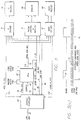
- FIG. 1 illustrates an embodiment of the prior art.
- the embodiment includes a graphics controller 10, a storage memory such as a VRAM 12 and stages 14 comprising a random access memory (RAM) and a digital-to-analog converter (DAC).
- the graphics controller 10 may be a central processing unit which transfers information into the VRAM 12 as indicated at 16. Information is in turn transferred from the VRAM 12 into the stages 14 (designated as "RAMDAC” in Figure as an acronym for random access memory and digital-to-analog converter).
- the random access memory may comprise a palette (also known as a look-up table) which is well known in the art.
- the transfer of information into the RAMDAC 14 is indicated at 18.
- a "/32" indication is provided adjacent the line 18 to indicate that there may be thirty two (32) bits in each byte of information.
- the analog output from the RAMDAC is indicated at 19. This output may be introduced to a monitor 20 for display on the face of a display screen in the monitor.
- the palette in the RAMDAC may have a plurality of positions each indicating an individual color.
- the color at each position may be indicated by a first plurality of bits indicating the primary color red, a second plurality of bits indicating the primary color blue and a third plurality of colors indicating the primary color green.
- the bits indicating each of the primary colors are converted to corresponding analog values in the RAMDAC.
- the respective intensities of the three primary colors at each pixel position controls the color generated at such pixel position on the face of the monitor 20.
- the graphics controller 10 introduces binary indications into successive positions in the VRAM 12. Each of these binary indication is comprised of a plurality of binary bits. Each plurality indicates a particular position to be selected in the palette.
- the information transferred from the graphics controller 10 to the VRAM 12 and from the VRAM to the RAMDAC 16 may be provided at a particular clock frequency as indicated by a line 22 extending from the graphics controller 10 to the VRAM 12 and the RAMDAC 14.
- Graphics information may be displayed on the screen of the monitor 20.
- the image on the face of the monitor 20 may be formed by a plurality of pixels in a raster scan. For example, twelve hundred and eighty (1280) pixels may be provided in each horizontal line in the raster scan and ten hundred and twenty four(1024) lines may be provided in such raster scan.
- the raster may be refreshed at a rate of seventy hertz (70 Hz). Under such circumstances, the pixels are presented at a frequency of one hundred and thirty two megahertz (132 Mhz).
- the VRAM is thirty two (32) bits wide, four (4) words each of eight (8) bits may be presented in parallel. This allows the information to be transferred serially from the VRAM at a frequency of thirty three megahertz (33 Mhz). Since each word comprises eight (8) bits, the palette may have two hundred and fifty six (256) different positions each indicating an individual color.
- Figure 1 (a) schematically indicates the clock signals on the line 22 as at 24 and schematically indicates the blanking interval 26 at the beginning of each line.
- Figure 2 schematically shows a system which is disclosed in EP-A-0610829 (published 17.8. 94).
- a graphics controller 40, a storage member (such as a VRAM 42) and stages 44 are included in the system.
- the stages 44 may include a shift register such as a first-in-first-out (FIFO) register and may also include a random access memory (RAM) and a digital-to-analog converter (DAC).
- FIFO first-in-first-out
- RAM random access memory
- DAC digital-to-analog converter
- This information may be graphics information in a first portion 42a of the VRAM and may also be standard interframe video information (SIF) such as NTSC or PAL video in a second portion 42b of the VRAM.
- SIF standard interframe video information
- the first and second portions of the VRAM are indicated schematically by a broken horizontal line in the VRAM 42.
- This information may illustratively have 320 pixels per horizontal line and may have 240 horizontal lines in each raster scan.
- the graphics information for a frame may be stored in one portion of the VRAM 42 as indicated at 42a and the standard interframe video information for a frame may be stored in a second portion 42b of the VRAM.
- the graphics information and the standard interframe video information are transferred from the graphics controller 40 into the VRAM 42 in parallel form.
- Each byte of parallel information may have thirty two (32) bits.
- the graphics information and the standard interframe video information are serially transferred from the VRAM 42.
- the graphics information in the portion 42a of the VRAM 42 is transferred, as in the embodiment shown in Figure 1, at a rate of thirty three megahertz (33 Mhz) by providing four (4) words, each of eight (8) bits.
- the transfer is made into the RAMDAC portion of the stages 42 in a manner similar to that disclosed above for the embodiment shown in Figure 1. This transfer occurs during the portion of each line in the raster scan in a monitor 46 other than the video blanking interval. This transfer is in synchronism with the rate of presentation of pixels on the screen of the video monitor 46. The transfer is accordingly at thirty three megahertz (33 Mhz). This transfer is indicated at 48a in Figure 2a.
- the VRAMs now being introduced into the market can transfer information serially out of the VRAM 42 at a rate of sixty six megahertz (66 Mhz). The transfer accordingly does not utilize the full capability of the VRAM 42.
- the standard video information (SIF) is transferred serially from the portion 42b of the VRAM 42 into the FIFO portion of the stages 44 at a frequency of sixty six megahertz (66 Mhz). This transfer is indicated at 48b in Figure 2a.
- the horizontal blanking interval constitutes only about twelve percent (12%) of the time in a line.
- the horizontal retrace period and the horizontal blanking interval are sufficiently long to transfer all of the standard interframe video information for a line into the FIFO portion of the stages 44. This is particularly true if the information transfer is at a rate of sixty six megahertz (66 Mhz).
- the information stored in the FIFO portion of the stages 44 for each line is converted into a line of twelve hundred and eighty (1280) pixels in the stages 44 by techniques known in the prior art.
- a multiplexer included in the stages 44 selects, in accordance with information from the controller 40, whether the graphics information in the RAM or the standard interframe information obtained from the FIFO will be converted by the DAC to analog information for display on the screen of the monitor 46.
- the video information in the portion 42b of the VRAM is transferred into the stages 44 at the graphics frequency of thirty three megahertz (33 Mhz).
- the system shown in Figure 2 and described above has certain important advantages. As described above, it uses only one (1) VRAM to store two (2) types (graphics and standard interframe video) information. It provides for the transfer of both types of information in each line in the raster scan and provides for the display of both types of information simultaneously in the successive frames on the screen of the monitor 46. For example, the graphics information may be displayed in the major portion of the raster scan and the standard interframe video information may be displayed in a window in the raster scan. However, the full transfer capabilities of the VRAM at sixty six megahertz (66 Mhz) are utilized for only a small (12%) portion of each line. Furthermore, only two (2) types of information can be presented. This is less than the number of different types of information that it is often desired to provide in a multimedia system.
- FIG 3 is a schematic diagram illustrating one embodiment of the invention.
- This embodiment includes a graphics controller 60 similar to that shown in Figures 1 and 2.
- Bytes of digital information are transferred from the graphics controller 60 to a storage member such as a VRAM 62 similar to that shown in Figures 1 and 2.
- Each byte may be thirty two (32) bits wide and may be provided through a bus 64.
- Each byte is transferred to a particular location in the VRAM 62 under the control of address information passing to the VRAM 62 through a pair of lines 66 and 68.
- a row address select (RAS) may be provided on the line 66 and a column address select (CAS) may be provided on the line 66.
- the digital information passing through the lines 64, 66 and 68 may be at the VRAM clock frequency of sixty six megahertz (66 Mhz). These clock signals are provided through a line 70.
- the digital information in the VRAM 62 is transferred from the VRAM serially at the clock frequency of sixty six megahertz (66 Mhz). Unlike the embodiment shown in Figure 2 in which this high clock rate was possible only during the blanking interval in each horizontal line in the raster scan, the high clock rate is essentially continuous in the embodiment shown in Figure 3.
- the only time that the clock is not at sixty six megahertz (66 Mhz) is when a serial register transfer is being made inside the VRAM at the request of the graphics controller 60. During this time, new data is being transferred from the storage location in the VRAM register to the VRAM serial data register. This occurs for only a few cycles of the clock frequency in each line in the raster scan.
- the blanking interval in each line in the raster scan is indicated at 70 in Figure 3(a).
- the serial transfer of data from the VRAM 62 at essentially the clock frequency of sixty six megahertz (66 Mhz) is indicated at 72 in Figure 3(a).
- the information transferred serially from the VRAM 62 at this clock frequency may represent a number of different media.
- the information may constitute television information in NTSC, PAL or SECAM form. This information is transferred to a television encoder 74 and is then transferred from the television encoder to a television receiver 76.
- the digital information may also be transferred from the VRAM 62 to stages 78.
- This information may have several different forms. It may constitute standard interframe video information (SIF). Actually, the standard interframe video interframe information may have several different forms. For example, SIF information may have 240 lines each of 320 pixels in a raster scan (designated as SIF1). Similarly, information designated as SIF2 may have 120 lines and 160 pixels in each line.
- the digital information transferred from the VRAM 62 may also be in graphics form.
- the graphics information may have several different formats. For example, when the graphics information is intended for a workstation, there may be 1024 rows and 1280 pixels in each row. When the graphics information is intended for a VGA format, there may be 4xx rows and 6xx pixels in each row. For a super VGA format, the number of rows may be 768 and the number of pixels in each row may be 1024.
- the stages 78 may receive other types of information in addition to the standard interframe video information and the graphics information. For example, digital information may be transferred from the VRAM 62 to the stages 78 to indicate cursor information.
- the information transferred to the stages 78 is introduced to a monitor 80 corresponding to the monitors 20 and 46 respectively shown in Figures 1 and 2. Audio information may also be transferred to an audio encoder 82 for storage and conversion to analog form and may then be transferred from these stages to an audio receiver 84. As will be appreciated and as will be seen from subsequent Figures, the stages 78 are shown in simplified form as a single stage but may actually constitute a plurality of different stages.
- Some control may accordingly have to be provided to direct the information from the VRAM 62 at different times to individual ones of the television encoder 74, the stages 78 (including standard interframe video, graphics and cursor encoders) and the audio encoder 82.
- This control is provided by a tag bus 86 which may provide four (4) bits in parallel. In the embodiment shown in Figure 3, the tag bus 86 provides these four (4) bits for each byte or packet of thirty two (32) bits from the VRAM 62. The four (4) bits are encoded to direct such byte or packet into the proper one of the different encoders.
- a line 88 also extends in Figure 3 from the stages 78 to the graphics controller 60 to synchronize the operation of the graphics controller in each line in the raster scan in providing for the passage of information serially from the VRAM 62 to the different encoders in the stages 78.
- different types of digital information may be transferred from the VRAM 62 to the different types of encoders shown schematically in Figure 3 and in additional detail in Figure 6.
- Such different types of digital information may include graphics, different types of standard interframe video (such as those designated as SIF1 and SIF2), audio, television (designated as NTSC only be way of illustration) and cursor.
- the information transferred from the VRAM 62 may also include what is designated in Figure 4 as a palette shadow.
- This information involves an updating of every position in the palette or look-up table at the end of each frame in the raster scan in the monitor 80 in Figure 3.
- the updating is provided in each position in the palette even though the color information in some positions in the palette remains unchanged. This is different from the updating provided in the prior art.
- the updating is generally provided at the end of each line and is only in selected positions.
- the updating of all of the positions in the palette at the end of each frame in the raster scan may be provided because the updating is occurring at the high frequency of sixty six (66) megahertz.
- the transfer of information from the VRAM 62 may occur in a particular sequence in each line in the raster scan in the monitor 80.
- This sequence is illustratively shown in Figure 5.
- the sequence in each line may be as follows: standard interframe video information (SIFI and STF2), graphics information, audio information and television information (designated as NTSC).
- SIFI and STF2 standard interframe video information
- graphics information graphics information
- audio information and television (NTSC) information may be synchronized at a particular time in each line.
- the audio information and the television (NTSC) information may occur after the standard interframe video information and the graphics information in each line but at a time unrelated to any synchronizing information, such as the blanking interval, in such line.
- NTSC information is specifically designated in Figure 5, other types of television information such as PAL or SECAM are within the scope of the invention.
- Figure 5 illustrates the sequence of the different types of digital information in each line.
- the standard interframe video information (SIF1 and SIF2) occurs first in each line. This is followed by the graphics information.
- the audio and television (e.g. NTSC) information then occur in each line.
- the cursor information occurs after the television (e.g. NTSC) information.
- the palette shadow information is provided to update the palette or look-up table for the graphics information in the next raster scan.
- the graphics data is transferred into a shift register such as a first-in-first out register 100 (e.g. FIFO) in Figure 6.
- a shift register such as a first-in-first out register 100 (e.g. FIFO) in Figure 6.
- FIFO 100 and other FIFO's in the embodiment shown in Figure 6 and in other Figures in this application are well known in the art. They receive and store bytes of information. These bytes of information are shifted through the FIFO 100 (and other FIFO's) in the same order as they are received. When the information introduced into the FIFO 100 has been shifted through the FIFO, the bytes of digital information are then transferred from the FIFO in the same order that they are received.
- the FIFO 100 for the graphics information has a capacity less than the number of pixels in each line. This causes the transfer of the bytes of binary graphics information into the FIFO 100 to be initiated at a particular instant in each line in the raster scan. This initiation of the transfer of the digital graphics information in each line into the FIFO 100 occurs at a particular time during the blanking interval 102 (see Figure 5) in each line. By initiating the transfer of the digital graphics information into the FIFO 100 at such time, substantially the full capacity of the FIFO 100 can be utilized in receiving the bytes of graphics information for the line without any of the graphics information being unable to be transferred into the FIFO because the FIFO has become filled. Furthermore, with this type of transfer, substantially the full capacity of the FIFO is used all of the time.
- the standard interframe video information is transferred into storage registers such as FIFO's 104 (for the SIF1) and 106 (for the SIF2) in Figure 6.
- the transfer of the standard interframe video information into the FIFO's 104 and 106 for each line may be initiated at a time 108 in Figure 5 before the blanking interval for the line.
- the FIFO's 104 and 106 may have a full capacity (rather than a partial capacity as for the FIFO 100) because the capacities of the FIFO's 104 and 106 are not very large. This results from the fact that there are only 320 pixels per line in SIF1 information and only 160 pixels per line in SIF2 information. This is in contrast to 1280 pixels per line in graphics information for display on the monitors in work stations.
- the transfers of the standard interframe video information and the graphics information may be initiated at particular times in each line in the raster scan in the monitor 80 in Figure 3.
- the transfer of the audio information for each line in the raster scan into the audio encoder 82 in Figure 3 may be initiated immediately after the transfer of the graphics information for that line has been completed.
- the transfer of the audio information may be initiated without reference to any particular time in each line.
- the capacity of the audio encoder 82 (which may be a FIFO) is somewhat limited. Because of this, when the audio encoder 82 has been substantially filled in a line, it sends a signal (designated as "Audio FF Full") on a line 110 in Figure 3 to the graphics controller 60. This signal causes the graphics controller 60 to instruct the VRAM 62 to stop sending bytes of digital audio information to the audio encoder 82 for that line.
- the transfer of the bytes of the digital television information may be initiated in each line after the transfer of the audio information in that line.
- the transfer of such bytes of digital television information in each line is made into the encoder 74 in Figure 3.
- the transfer may be made on any asynchronous basis in each line, in other words, without reference to any particular time in such line.
- the capacity of the encoder 74 may be somewhat limited. Because of this, the encoder sends a signal through a line 112 in Figure 3 to have the graphics controller 60 discontinue the transfer of television information into the encoder 74 from the VRAM 62 in any line when the encoder has been filled to a particular capacity in that line. This signal is designated in Figure 3 as "NTSC-FF-FULL".
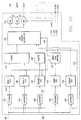
- stages 78 in Figure 3 are shown in additional detail in Figure 6. This is indicated by broken lines which extend around the stages shown in Figure 6 and which have the numerical designation 78.
- the stages 78 in Figure 3 may include the stages 100, 104 and 106 in Figure 6. They may also include FIFO's 114 and 116 in Figure 6.
- the FIFO 116 receives the cursor information in a particular line in the raster scan.
- the stages 100, 104, 106 and 116 may receive bytes of digital information through a line 118 (also shown in Figure 3) from the VRAM 62.
- the FIFO 114 may receive the timing and control information from the tag bus 84 also shown in Figure 3.
- the information from the tag bus 84 may pass through an amplifier 120 in Figure 6 to decoders 122, 124, 126 ,128 and 130 respectively for the FIFO's 104, 106, 100, 114 and 116.
- Decoders such as the decoders 122, 124, 126, 128 and 130 are well known in the art. They decode the four (4) bits of digital information in the tag bus 84 for each byte of digital information in the bus 118. The decoded information controls which one of the FIFO's 100, 104, 106 and 116 will receive and store that byte of information.
- the decoder 128 decodes the bytes of the digital information in the tag bus 84 to provide timing and control information in binary form. This timing and control information passes from the decoder 128 into the FIFO 114.
- the information in the FIFO 114 then passes into a timing state machine 134 which processes this information to produce various timing and control signals for each line in the raster scan.
- the timing state machine 134 may produce the synchronizing signal on the line 88 to initiate the transfer of the standard interframe video information in each line into the FIFO's 104 and 106 at the time indicated at 108 in Figure 5(a).
- the timing state machine 134 may also produce on a line 136 the horizontal sync signal for each line in the raster scan and on a line 138 the vertical sync signal after each such raster scan.
- the timing state machine may also produce the horizontal blanking signal (see 70 in Figure 3a and 102 in Figure 5) on a line 154 in Figure 6.
- the timing state machine 134 may also produce signals on a line 135 for introduction to the FIFO's 100, 104, 106 and 116. These signals may activate individual ones of the FIFO's 100, 104, 106 and 116 to provide for the passage of signals from these FIFO's at times determined by the timing state machine.
- the signals from the standard interframe video FIFO's 104 and 106 pass to a scaler 144; the signals from the graphics FIFO pass to a palette 146; and the signals from the cursor FIFO 116 pass to a cursor palette 147.
- the timing state machine 134 may additionally produce a priority signal on a line 140. This signal is introduced to a pixel priority multiplexer 142 to control whether the standard interframe video information from one of the FIFO's 104 and 106 or the graphics information from the FIFO 100 will pass through the multiplexer at each instant.
- the information in the FIFO's 104 and 106 may be initially introduced to the scaler 144 and the scaled information may be then passed to the multiplexer 142.
- the scaler 144 is well known in the art and different examples of the scaler 144 are disclosed in some detail in EP-A-0 610 829 (published 17.8.94).
- the scaler increases the number of bytes in the FIFO's 104 and 106 for each line in the raster scan into a number of bytes corresponding to the number of bytes in each line in the graphics information.
- the bytes of the digital information in the FIFO 100 for each line may be introduced to the palette 146 to select the individual positions in the palette for the passage of color information to the pixel priority multiplexer 142.
- the palette 146 corresponds in construction to the palette in the RAMDAC 14 in Figure 1 and to the palette in the stages 44 in Figure 2.
- the FIFO 116 passes information to the cursor palette 147 which passes the cursor information to the multiplexer 142 for passage through the multiplexer.
- the passage of the cursor information from the palette 147 through the multiplexer 142 may be controlled by the priority signal on the line 140.
- the bytes of information passing through the multiplexer 142 from the scaler 144, the palette 146 and the palette 147 may be introduced to digital-to-analog converters 148, 150 and 152 respectively for the primary colors red, green and blue.
- the analog signals from the converters 148, 150 and 152 then pass to the monitor 80 shown in Figure 3.
- the converters 148, 150 and 152 may receive a blanking signal on the line 154 from the timing state machine 134. The blanking signal blanks the converters 148, 150 and 152 during each line in the raster scan.
- each byte of information from the timing FIFO 114 may comprise thirty two (32) bits. Of these, twenty (20) bits may be introduced to stages 160 (designated as "state") which produce the horizontal sync signal on the line 136, the vertical sync signal on the line 138, the blanking signal on the line 154, the priority signal on the line 140 and the signals on the lines 135 to the FIFO's 100, 104, 106 and 116.
- the timing of these signals is provided by the other twelve (12) bits in each byte from the timing FIFO 114. These bits are introduced to a counter 162 which is preset to a particular value.
- the counter 162 then counts downwardly by an integer through a documenting stage 164 every time that a pixel clock signal is produced on the line 70 (also shown in Figure 3).
- the count from the counter corresponds to a count preset in a comparator 166.
- the comparator 166 then produces a signal on a line 168 to provide for the passage of the next byte of thirty two (32) bits from the FIFO 114 to the stages 160 and the counter 162.
- FIG 8 schematically illustrates an embodiment in which a dynamic random access memory (DRAM) 170 may be used instead of a VRAM as in the previous embodiment.
- the DRAM 170 is advantageous because the cost of a DRAM is approximately one halt (1/2) of the cost of a VRAM of the same size.
- the embodiment shown in Figure 8 is also advantageous because all of the transfer of information, even from the DRAM 170, to PACDAC stages 172 is in parallel. This tends to increase the speed of operation of the system shown in Figure 8.
- a DRAM is disadvantageous in comparison to a VRAM because first information cannot be simultaneously introduced into a DRAM while second information is being transferred out of the DRAM.
- the data bandwidth of the system shown in Figure 8 is not as great as that of Figure 3 because only the random access port of the DRAM 170 is used and the bandwidth of the DRAM is typically less than half of the sixty six megahertz (66 Mhz) bandwidth in the VRAMs which are being introduced into the market.
- the embodiment shown in Figure 8 includes a graphics controller 172 similar to the graphics controller 60 shown in Figure 3. It also includes stages 174 designated as "PACDAC". These stages correspond to the stages 78 shown in Figure 3.
- PACDAC stages 174 designated as "PACDAC".
- stages 174 correspond to the stages 78 shown in Figure 3.
- Each of the controller 172, the DRAM 170 and the PACDAC stages 174 can communicate with the others.
- the transfer of information into the DRAM 170 from the controller 172 and out of the DRAM 172 is controlled by address signals on a bus 175.
- the signals on the bus 175 correspond to the signals on the lines 66 and 68 in Figure 3.
- a tag bus 176 is provided in Figure 8 to control the destination of the bytes of the different types of information in the DRAM 170 and the time in each line for the transfer of such bytes.
- the PACDAC stages 174 can have the construction shown in Figure 6 and the timing state machine can have the construction shown in Figure 7.
- the different types of information can be provided in the sequence shown in Figure 5 and the timing for the standard interframe video information in each line can be provided as by a pulse on a line 175 corresponding to the pulse 108 in Figure 5.
- the bytes of digital information transferred between the DRAM 170, the graphics controller 172 and the PACDAC stages 174 on a bus 177 may have sixty four (64) bits.
- the DRAM 170 may accordingly be formed from four (4) DRAMs in parallel, each DRAM having sixteen (16) bits.
- the FIFO for the graphics information may have a limited capacity to conserve cost and space.
- the FIFO's for the television (e.g. NTSC) and audio information may also have limited capacities as in the embodiment shown in Figure 3. This is indicated by the designation of "NTSC-FF-FULL" for a line 178 and "AUDIO-FF-FULL" for a line 180.
- Signals may accordingly be produced respectively on the lines 178 and 180 to instruct the graphics controller to interrupt the transfer of information from the DRAM 170 into the television and audio FIFO's when these FIFO's become filled to a particular limit.
- Clock signals may be produced on a line 182 in the embodiment shown in Figure 8 in a manner similar to the production of clock signals on the line 70 in the embodiment shown in Figure 3.
- the embodiment shown in Figure 9 is intended to be used for a system designated as "RAMBUS.”
- the "RAMBUS" system is well known in the prior art.
- the embodiment shown in Figure 9 represents an improvement in the "RAMBUS" system of the prior art.
- the system shown in Figure 9A includes a graphics controller 190, PACDAC stages 192 and DRAMs 194 as in the embodiments shown in Figures 3 and 8.
- the controller 190, the stages 192 and the DRAMs 194 may be connected by a common bus 196. Packets or bytes of digital information may pass through the bus 196 between the controller 190, the stages 192 and the DRAMs 194. Each of these bytes or packets may have ten (10) bits.
- Eight (8) of the ten (10) bits in each byte or packet in the embodiment of Figure 9 may comprise data.
- the other two (2) bits in each byte or packet may be used to provide parity checking and to provide special signalling.
- the two (2) bits for special signalling in individual ones of the bytes or packets may be used to indicate that the eight (8) data bits in such bytes or packets provide the information provided in the Tag Bus in the embodiments shown in Figures 3 and 8.
- such eight (8) bits specify the destination of the data in the subsequent bytes or packets and specify the timing for the information in the subsequent bytes or packets.
- the graphics controller 190 in Figure 9 may have the same construction as the graphics controller in the embodiments shown in Figures 2 and 8.
- the DRAMs 194 in the embodiment of Figure 9 may have the same construction as the DRAM 170 in the embodiment shown in Figure 8. However, the DRAMs 190 may be only ten (10) bits wide rather than sixty four (64) bits wide as in the embodiment shown in Figure 8.
- the PACDAC stages 192 shown in Figure 9 are substantially the same as the PACDAC stages shown in Figure 3 except that, as described above, a Tag Bus is not included in the embodiment shown in Figure 9. Because of this, the PACDAC stages 192 may have the construction shown in Figure 10. They are included within broken lines designated as 192 in Figure 10.
- the bytes or packets on the bus 196 from the graphics controller 190 may pass to the decoder 228 which decodes the bits indicating that the eight (8) data bits in the bytes or packets contain timing and control information rather than digital information for the other FIFO's. These eight (8) bits in the timing and control packets may then pass to the timing FIFO 214. The eight (8) bits may then pass from the FIFO 214 to the timing state machine 234 which produces the timing and control signals indicating the destination of the subsequent bytes or packets of information. The destination signals may be produced by the timing state machine 234 on lines 235. These signals may accordingly activate one of the decoders 222, 224, 226 and 230. The activated one of the decoders 222, 224, 226 and 230 may then pass the subsequent bytes or packets of information on the line 218 to the respective ones of the FIFO's 200, 204, 206 and 216.
- the scaler 244 acts on these signals to scale the number of pixels in each line upwardly and the signals from the scaler 244 may then pass to the pixel priority multiplexer 242.
- the signals from the graphics FIFO 200 may select positions in the palette 246 and these signals may pass to the pixel priority multiplexer 242.
- the signals in the FIFO 216 may select positions in the cursor palette 246 and the signals from the palette may pass to the pixel priority multiplexer 242.
- the pixel priority multiplexer 242 may pass the signals from individual ones of the scaler 244, the palette 246 and the cursor FIFO 216 in accordance with signals on the line 240 from the timing state machine 234.
- the signals passing through the pixel priority multiplexer 242 are introduced to the color converters 248, 250 and 252.
- the passage of the signals from the converters 248, 250 and 252 and the display of the signals on the monitor 280 are controlled by signals produced on the lines 236, 238 and 254 by the timing state machine 234.
- the apparatus disclosed above has several important advantages. It provides for an efficient processing of different types of information including standard interframe video information, graphics information, television information, audio information and cursor information.
- the system provides for such processing either with a VRAM or a DRAM.
- the system employs a data bus for the different types of information and employs a tag bus for the timing and control information.
- the system employs a common bus for all of the sub-systems in the system and uses individual bits in each byte or packet on such bus to indicate whether the data bits in such byte or packet represent media information or timing and control information.
Abstract
Description
- The invention relates to a method for processing data, in a multimedia graphics system for use with a monitor for displaying information as indicated in
claims 1 and 5. - Significant advances have been made in recent years in providing displays of a video information on a video monitor or screen. For example, graphics information has been displayed oh a video monitor with enhanced resolution and fidelity as a result of significant advances in the processing of the digital information representing such colors and in the conversion of such digital information into an analog form. Such information has often been processed in digital form and thereafter converted to analog form in a personal computer or work station. In recent years, video information has been simultaneously displayed with the graphics information in such personal computers and work stations. For example, video information has been displayed in a window on the face of the video monitor of the personal computer or work station while graphics information has been displayed on the remainder of the monitor face.
- In recent years there have also been significant strides in using miniaturized computers such as personal computers and work stations in processing information involving multimedia applications. These multimedia applications may take many different forms. For example, they may involve graphics, television, facsimile and/or audio. In spite of these advances, a suitable system does not exist which is sufficiently flexible to process different types of information efficiently, inexpensively and reliably. For example, the systems now in use are not capable of switching efficiently, inexpensively and reliably between different types of presentations such as graphics, video and audio. This has been particularly true when information from more than one type of media (e.g. graphics, video, television and audio) is to be presented simultaneously. This has limited the utility of the systems now in use. Such limitations exist now in multimedia equipment even though considerable amounts of money have been expended, and considerable effort has been devoted, through the years, and particularly in recent years, to develop a satisfactory multimedia system.
- In one embodiment of this invention, bytes of different types of digital information including standard interframe video (SIF), graphics, television and audio are transferred between a controller, a storage memory and shift registers (e.g. FIFO's) individually associated with the different information types. For a VRAM memory, information is transferred in parallel, controlled by tag bus information, from the controller to the memory and then serially from the memory to the FIFO's, all at a frequency higher than a clock frequency in a monitor raster scan.
- The tag bus information is decoded and introduced to an additional FIFO. A state machine processes such additional FIFO information and transfers the digital information to the different FIFO's at times controlled in each line by such additional FIFO-e.g. particular times in each line for the SIF and the graphics and thereafter, for television and audio, at times unrelated to any times in such line.
- The graphics transfer is timed to substantially fill, but not overflow, the limited capacity of the associated FIFO in each line. Their limited capacities cause the television and audio FIFO's to stop receiving bytes when filled to particular limits. For a DRAM memory, information is transferred, dependent upon tag bus information, in parallel between the controller, memory and FIFO's at the clock frequency. In a "Rambus" system, a bus common with the controller, memory and FIFO's provides control and timing bytes. The information in successive bytes is transferred through the common bus to the controller, memory and FIFO's dependent upon such timing and control information in such bytes.
- In the drawings:
- Figure 1 is a schematic block diagram of a system of the prior art;
- Figure 1(a) shows wave forms at strategic terminals in the system shown in Figure 1;
- Figure 2 is a schematic block diagram of another system of the prior art, this system being shown and disclosed in a patent application recently filed in the Patent Office by the assignee of record in this application;
- Figure 2(a) shows wave forms at strategic terminals in the system shown in Figure 2;
- Figure 3 is a schematic block diagram of a system constituting one embodiment of the invention;
- Figure 3(a) shows waveforms at strategic terminals in the system shown in Figure 3;
- Figure 4 is a table illustrating the different types of digital information processed by the system shown in Figure 3;
- Figure 5 illustrates the sequence of signals processed by the system of Figure 3 in each line in a raster scan in a monitor included in Figure 3;
- Figure 5(a) illustrates wave forms at strategic terminals in the system of Figure 3;
- Figure 6 is an expanded schematic block diagram illustrating one of the blocks in Figure 3 in additional detail;
- Figure 7 is an expanded schematic block diagram illustrating one of the blocks in Figure 6 in additional detail;
- Figure 8 is a schematic block diagram of another embodiment of the invention;
- Figure 9 is a schematic block diagram of a further embodiment of the invention; and
- Figure 10 is an expanded schematic block diagram illustrating one of the blocks in Figure 9 in additional detail.
-
- Figure 1 illustrates an embodiment of the prior art. The embodiment includes a
graphics controller 10, a storage memory such as aVRAM 12 andstages 14 comprising a random access memory (RAM) and a digital-to-analog converter (DAC). Thegraphics controller 10 may be a central processing unit which transfers information into theVRAM 12 as indicated at 16. Information is in turn transferred from theVRAM 12 into the stages 14 (designated as "RAMDAC" in Figure as an acronym for random access memory and digital-to-analog converter). The random access memory may comprise a palette (also known as a look-up table) which is well known in the art. The transfer of information into the RAMDAC 14 is indicated at 18. A "/32" indication is provided adjacent theline 18 to indicate that there may be thirty two (32) bits in each byte of information. The analog output from the RAMDAC is indicated at 19. This output may be introduced to amonitor 20 for display on the face of a display screen in the monitor. - The palette in the RAMDAC may have a plurality of positions each indicating an individual color. The color at each position may be indicated by a first plurality of bits indicating the primary color red, a second plurality of bits indicating the primary color blue and a third plurality of colors indicating the primary color green. When an individual position in the palette is selected, the bits indicating each of the primary colors are converted to corresponding analog values in the RAMDAC. The respective intensities of the three primary colors at each pixel position controls the color generated at such pixel position on the face of the
monitor 20. - The
graphics controller 10 introduces binary indications into successive positions in theVRAM 12. Each of these binary indication is comprised of a plurality of binary bits. Each plurality indicates a particular position to be selected in the palette. The information transferred from thegraphics controller 10 to theVRAM 12 and from the VRAM to theRAMDAC 16 may be provided at a particular clock frequency as indicated by aline 22 extending from thegraphics controller 10 to theVRAM 12 and theRAMDAC 14. - Graphics information may be displayed on the screen of the
monitor 20. When the RAMDAC is included in a work station (not shown), the image on the face of themonitor 20 may be formed by a plurality of pixels in a raster scan. For example, twelve hundred and eighty (1280) pixels may be provided in each horizontal line in the raster scan and ten hundred and twenty four(1024) lines may be provided in such raster scan. The raster may be refreshed at a rate of seventy hertz (70 Hz). Under such circumstances, the pixels are presented at a frequency of one hundred and thirty two megahertz (132 Mhz). When the VRAM is thirty two (32) bits wide, four (4) words each of eight (8) bits may be presented in parallel. This allows the information to be transferred serially from the VRAM at a frequency of thirty three megahertz (33 Mhz). Since each word comprises eight (8) bits, the palette may have two hundred and fifty six (256) different positions each indicating an individual color. - It may be desired to update the palette in the RAMDAC 14. This may be accomplished during the horizontal retrace period at the end of each line or during the horizontal blanking interval at the beginning of each line. The horizontal retrace period is relatively short but the horizontal blanking interval in each line is approximately twelve percent (12%) of the duration of the line. The palette may also be updated during the vertical retrace period at the end of each raster scan. The vertical retrace period is considerably longer than each horizontal retrace period. Figure 1 (a) schematically indicates the clock signals on the
line 22 as at 24 and schematically indicates the blankinginterval 26 at the beginning of each line. - The system shown schematically in Figure 1 and discussed above has had extensive usage in the prior art. It is advantageous in that it is relatively simple and reliable. It is disadvantageous in that it provides only a limited number of pseudo colors rather than real colors. Furthermore, it is able to provide only graphics information for display on the
monitor 20. It is also not capable of fully utilizing the advantages offered by the latest models of VRAMS which are just being introduced to the market. These VRAMS are capable of operating at a frequency of sixty six megahertz (66 Mhz). This is in contrast to the maximum frequency response of thirty three megahertz (33 Mhz) for the VRAMs now on the market. - Figure 2 schematically shows a system which is disclosed in EP-A-0610829 (published 17.8. 94).
- A
graphics controller 40, a storage member (such as a VRAM 42) and stages 44 are included in the system. Thestages 44 may include a shift register such as a first-in-first-out (FIFO) register and may also include a random access memory (RAM) and a digital-to-analog converter (DAC). - Information is introduced into the VRAM 42 from the
graphics controller 40 in the embodiment shown in Figure 2. This information may be graphics information in a first portion 42a of the VRAM and may also be standard interframe video information (SIF) such as NTSC or PAL video in a second portion 42b of the VRAM. The first and second portions of the VRAM are indicated schematically by a broken horizontal line in the VRAM 42. This information may illustratively have 320 pixels per horizontal line and may have 240 horizontal lines in each raster scan. The graphics information for a frame may be stored in one portion of the VRAM 42 as indicated at 42a and the standard interframe video information for a frame may be stored in a second portion 42b of the VRAM. This is advantageous over the prior art because it eliminates the need for a separate storage memory to store the standard interframe video information. The graphics information and the standard interframe video information are transferred from thegraphics controller 40 into the VRAM 42 in parallel form. Each byte of parallel information may have thirty two (32) bits. - The graphics information and the standard interframe video information are serially transferred from the VRAM 42. The graphics information in the portion 42a of the VRAM 42 is transferred, as in the embodiment shown in Figure 1, at a rate of thirty three megahertz (33 Mhz) by providing four (4) words, each of eight (8) bits. The transfer is made into the RAMDAC portion of the stages 42 in a manner similar to that disclosed above for the embodiment shown in Figure 1. This transfer occurs during the portion of each line in the raster scan in a
monitor 46 other than the video blanking interval. This transfer is in synchronism with the rate of presentation of pixels on the screen of thevideo monitor 46. The transfer is accordingly at thirty three megahertz (33 Mhz). This transfer is indicated at 48a in Figure 2a. - However, as previously indicated, the VRAMs now being introduced into the market can transfer information serially out of the VRAM 42 at a rate of sixty six megahertz (66 Mhz). The transfer accordingly does not utilize the full capability of the VRAM 42. During the horizontal retrace and the horizontal blanking interval in each line in the raster scan in the
monitor 46, the standard video information (SIF) is transferred serially from the portion 42b of the VRAM 42 into the FIFO portion of thestages 44 at a frequency of sixty six megahertz (66 Mhz). This transfer is indicated at 48b in Figure 2a. - The horizontal blanking interval constitutes only about twelve percent (12%) of the time in a line. However, since there are only three hundred and twenty (320) pixels in a line in standard interframe video information, the horizontal retrace period and the horizontal blanking interval are sufficiently long to transfer all of the standard interframe video information for a line into the FIFO portion of the
stages 44. This is particularly true if the information transfer is at a rate of sixty six megahertz (66 Mhz). The information stored in the FIFO portion of thestages 44 for each line is converted into a line of twelve hundred and eighty (1280) pixels in thestages 44 by techniques known in the prior art. A multiplexer included in the stages 44 (but not specifically shown) then selects, in accordance with information from thecontroller 40, whether the graphics information in the RAM or the standard interframe information obtained from the FIFO will be converted by the DAC to analog information for display on the screen of themonitor 46. The video information in the portion 42b of the VRAM is transferred into thestages 44 at the graphics frequency of thirty three megahertz (33 Mhz). - The system shown in Figure 2 and described above has certain important advantages. As described above, it uses only one (1) VRAM to store two (2) types (graphics and standard interframe video) information. It provides for the transfer of both types of information in each line in the raster scan and provides for the display of both types of information simultaneously in the successive frames on the screen of the
monitor 46. For example, the graphics information may be displayed in the major portion of the raster scan and the standard interframe video information may be displayed in a window in the raster scan. However, the full transfer capabilities of the VRAM at sixty six megahertz (66 Mhz) are utilized for only a small (12%) portion of each line. Furthermore, only two (2) types of information can be presented. This is less than the number of different types of information that it is often desired to provide in a multimedia system. - Figure 3 is a schematic diagram illustrating one embodiment of the invention. This embodiment includes a
graphics controller 60 similar to that shown in Figures 1 and 2. Bytes of digital information are transferred from thegraphics controller 60 to a storage member such as aVRAM 62 similar to that shown in Figures 1 and 2. Each byte may be thirty two (32) bits wide and may be provided through abus 64. Each byte is transferred to a particular location in theVRAM 62 under the control of address information passing to theVRAM 62 through a pair oflines line 66 and a column address select (CAS) may be provided on theline 66. The digital information passing through thelines line 70. - The digital information in the
VRAM 62 is transferred from the VRAM serially at the clock frequency of sixty six megahertz (66 Mhz). Unlike the embodiment shown in Figure 2 in which this high clock rate was possible only during the blanking interval in each horizontal line in the raster scan, the high clock rate is essentially continuous in the embodiment shown in Figure 3. The only time that the clock is not at sixty six megahertz (66 Mhz) is when a serial register transfer is being made inside the VRAM at the request of thegraphics controller 60. During this time, new data is being transferred from the storage location in the VRAM register to the VRAM serial data register. This occurs for only a few cycles of the clock frequency in each line in the raster scan. - The blanking interval in each line in the raster scan is indicated at 70 in Figure 3(a). The serial transfer of data from the
VRAM 62 at essentially the clock frequency of sixty six megahertz (66 Mhz) is indicated at 72 in Figure 3(a). The information transferred serially from theVRAM 62 at this clock frequency may represent a number of different media. For example, the information may constitute television information in NTSC, PAL or SECAM form. This information is transferred to atelevision encoder 74 and is then transferred from the television encoder to atelevision receiver 76. - The digital information may also be transferred from the
VRAM 62 to stages 78. This information may have several different forms. It may constitute standard interframe video information (SIF). Actually, the standard interframe video interframe information may have several different forms. For example, SIF information may have 240 lines each of 320 pixels in a raster scan (designated as SIF1). Similarly, information designated as SIF2 may have 120 lines and 160 pixels in each line. - The digital information transferred from the
VRAM 62 may also be in graphics form. The graphics information may have several different formats. For example, when the graphics information is intended for a workstation, there may be 1024 rows and 1280 pixels in each row. When the graphics information is intended for a VGA format, there may be 4xx rows and 6xx pixels in each row. For a super VGA format, the number of rows may be 768 and the number of pixels in each row may be 1024. Thestages 78 may receive other types of information in addition to the standard interframe video information and the graphics information. For example, digital information may be transferred from theVRAM 62 to thestages 78 to indicate cursor information. - The information transferred to the
stages 78 is introduced to amonitor 80 corresponding to themonitors audio encoder 82 for storage and conversion to analog form and may then be transferred from these stages to anaudio receiver 84. As will be appreciated and as will be seen from subsequent Figures, thestages 78 are shown in simplified form as a single stage but may actually constitute a plurality of different stages. - Some control may accordingly have to be provided to direct the information from the
VRAM 62 at different times to individual ones of thetelevision encoder 74, the stages 78 (including standard interframe video, graphics and cursor encoders) and theaudio encoder 82. This control is provided by atag bus 86 which may provide four (4) bits in parallel. In the embodiment shown in Figure 3, thetag bus 86 provides these four (4) bits for each byte or packet of thirty two (32) bits from theVRAM 62. The four (4) bits are encoded to direct such byte or packet into the proper one of the different encoders. Aline 88 also extends in Figure 3 from thestages 78 to thegraphics controller 60 to synchronize the operation of the graphics controller in each line in the raster scan in providing for the passage of information serially from theVRAM 62 to the different encoders in thestages 78. - As illustrated in Figure 4 and as discussed above, different types of digital information may be transferred from the
VRAM 62 to the different types of encoders shown schematically in Figure 3 and in additional detail in Figure 6. Such different types of digital information may include graphics, different types of standard interframe video (such as those designated as SIF1 and SIF2), audio, television (designated as NTSC only be way of illustration) and cursor. - The information transferred from the
VRAM 62 may also include what is designated in Figure 4 as a palette shadow. This information involves an updating of every position in the palette or look-up table at the end of each frame in the raster scan in themonitor 80 in Figure 3. The updating is provided in each position in the palette even though the color information in some positions in the palette remains unchanged. This is different from the updating provided in the prior art. In the prior art, the updating is generally provided at the end of each line and is only in selected positions. The updating of all of the positions in the palette at the end of each frame in the raster scan may be provided because the updating is occurring at the high frequency of sixty six (66) megahertz. - The transfer of information from the
VRAM 62 may occur in a particular sequence in each line in the raster scan in themonitor 80. This sequence is illustratively shown in Figure 5. The sequence in each line may be as follows: standard interframe video information (SIFI and STF2), graphics information, audio information and television information (designated as NTSC). The standard interframe video information and the graphics information may be synchronized at a particular time in each line. The audio information and the television (NTSC) information may occur after the standard interframe video information and the graphics information in each line but at a time unrelated to any synchronizing information, such as the blanking interval, in such line. It will be appreciated that, although NTSC information is specifically designated in Figure 5, other types of television information such as PAL or SECAM are within the scope of the invention. - Figure 5 illustrates the sequence of the different types of digital information in each line. As will be seen, the standard interframe video information (SIF1 and SIF2) occurs first in each line. This is followed by the graphics information. The audio and television (e.g. NTSC) information then occur in each line. For the line in each raster scan where the cursor appears, the cursor information occurs after the television (e.g. NTSC) information. During the vertical retrace interval in each raster scan, the palette shadow information is provided to update the palette or look-up table for the graphics information in the next raster scan.
- As shown in Figure 5, the graphics data is transferred into a shift register such as a first-in-first out register 100 (e.g. FIFO) in Figure 6. The
FIFO 100 and other FIFO's in the embodiment shown in Figure 6 and in other Figures in this application are well known in the art. They receive and store bytes of information. These bytes of information are shifted through the FIFO 100 (and other FIFO's) in the same order as they are received. When the information introduced into theFIFO 100 has been shifted through the FIFO, the bytes of digital information are then transferred from the FIFO in the same order that they are received. - The
FIFO 100 for the graphics information has a capacity less than the number of pixels in each line. This causes the transfer of the bytes of binary graphics information into theFIFO 100 to be initiated at a particular instant in each line in the raster scan. This initiation of the transfer of the digital graphics information in each line into theFIFO 100 occurs at a particular time during the blanking interval 102 (see Figure 5) in each line. By initiating the transfer of the digital graphics information into theFIFO 100 at such time, substantially the full capacity of theFIFO 100 can be utilized in receiving the bytes of graphics information for the line without any of the graphics information being unable to be transferred into the FIFO because the FIFO has become filled. Furthermore, with this type of transfer, substantially the full capacity of the FIFO is used all of the time. - The standard interframe video information is transferred into storage registers such as FIFO's 104 (for the SIF1) and 106 (for the SIF2) in Figure 6. The transfer of the standard interframe video information into the FIFO's 104 and 106 for each line may be initiated at a
time 108 in Figure 5 before the blanking interval for the line. The FIFO's 104 and 106 may have a full capacity (rather than a partial capacity as for the FIFO 100) because the capacities of the FIFO's 104 and 106 are not very large. This results from the fact that there are only 320 pixels per line in SIF1 information and only 160 pixels per line in SIF2 information. This is in contrast to 1280 pixels per line in graphics information for display on the monitors in work stations. - As will be seen from Figure 5 and from the discussion above, the transfers of the standard interframe video information and the graphics information may be initiated at particular times in each line in the raster scan in the
monitor 80 in Figure 3. The transfer of the audio information for each line in the raster scan into theaudio encoder 82 in Figure 3 may be initiated immediately after the transfer of the graphics information for that line has been completed. However, the transfer of the audio information may be initiated without reference to any particular time in each line. The capacity of the audio encoder 82 (which may be a FIFO) is somewhat limited. Because of this, when theaudio encoder 82 has been substantially filled in a line, it sends a signal (designated as "Audio FF Full") on aline 110 in Figure 3 to thegraphics controller 60. This signal causes thegraphics controller 60 to instruct theVRAM 62 to stop sending bytes of digital audio information to theaudio encoder 82 for that line. - In like manner, the transfer of the bytes of the digital television information may be initiated in each line after the transfer of the audio information in that line. The transfer of such bytes of digital television information in each line is made into the
encoder 74 in Figure 3. As with the audio information, the transfer may be made on any asynchronous basis in each line, in other words, without reference to any particular time in such line. The capacity of theencoder 74 may be somewhat limited. Because of this, the encoder sends a signal through aline 112 in Figure 3 to have thegraphics controller 60 discontinue the transfer of television information into theencoder 74 from theVRAM 62 in any line when the encoder has been filled to a particular capacity in that line. This signal is designated in Figure 3 as "NTSC-FF-FULL". - The
stages 78 in Figure 3 are shown in additional detail in Figure 6. This is indicated by broken lines which extend around the stages shown in Figure 6 and which have thenumerical designation 78. As previously described, thestages 78 in Figure 3 may include thestages FIFO 116 receives the cursor information in a particular line in the raster scan. Thestages VRAM 62. In contrast, theFIFO 114 may receive the timing and control information from thetag bus 84 also shown in Figure 3. - The information from the
tag bus 84 may pass through anamplifier 120 in Figure 6 todecoders decoders tag bus 84 for each byte of digital information in thebus 118. The decoded information controls which one of the FIFO's 100, 104, 106 and 116 will receive and store that byte of information. Furthermore, thedecoder 128 decodes the bytes of the digital information in thetag bus 84 to provide timing and control information in binary form. This timing and control information passes from thedecoder 128 into theFIFO 114. - The information in the
FIFO 114 then passes into atiming state machine 134 which processes this information to produce various timing and control signals for each line in the raster scan. For example, thetiming state machine 134 may produce the synchronizing signal on theline 88 to initiate the transfer of the standard interframe video information in each line into the FIFO's 104 and 106 at the time indicated at 108 in Figure 5(a). Thetiming state machine 134 may also produce on aline 136 the horizontal sync signal for each line in the raster scan and on aline 138 the vertical sync signal after each such raster scan. The timing state machine may also produce the horizontal blanking signal (see 70 in Figure 3a and 102 in Figure 5) on aline 154 in Figure 6. - The
timing state machine 134 may also produce signals on aline 135 for introduction to the FIFO's 100, 104, 106 and 116. These signals may activate individual ones of the FIFO's 100, 104, 106 and 116 to provide for the passage of signals from these FIFO's at times determined by the timing state machine. The signals from the standard interframe video FIFO's 104 and 106 pass to ascaler 144; the signals from the graphics FIFO pass to apalette 146; and the signals from thecursor FIFO 116 pass to acursor palette 147. - The
timing state machine 134 may additionally produce a priority signal on aline 140. This signal is introduced to apixel priority multiplexer 142 to control whether the standard interframe video information from one of the FIFO's 104 and 106 or the graphics information from theFIFO 100 will pass through the multiplexer at each instant. The information in the FIFO's 104 and 106 may be initially introduced to thescaler 144 and the scaled information may be then passed to themultiplexer 142. Thescaler 144 is well known in the art and different examples of thescaler 144 are disclosed in some detail in EP-A-0 610 829 (published 17.8.94). - The scaler increases the number of bytes in the FIFO's 104 and 106 for each line in the raster scan into a number of bytes corresponding to the number of bytes in each line in the graphics information.
- The bytes of the digital information in the
FIFO 100 for each line may be introduced to thepalette 146 to select the individual positions in the palette for the passage of color information to thepixel priority multiplexer 142. Thepalette 146 corresponds in construction to the palette in theRAMDAC 14 in Figure 1 and to the palette in thestages 44 in Figure 2. In like manner, theFIFO 116 passes information to thecursor palette 147 which passes the cursor information to themultiplexer 142 for passage through the multiplexer. The passage of the cursor information from thepalette 147 through themultiplexer 142 may be controlled by the priority signal on theline 140. - The bytes of information passing through the
multiplexer 142 from thescaler 144, thepalette 146 and thepalette 147 may be introduced to digital-to-analog converters converters monitor 80 shown in Figure 3. Theconverters line 154 from thetiming state machine 134. The blanking signal blanks theconverters - The
timing state machine 134 is shown in additional detail in Figure 7 as being included within broken lines designated as 134. As shown in Figure 7, each byte of information from thetiming FIFO 114 may comprise thirty two (32) bits. Of these, twenty (20) bits may be introduced to stages 160 (designated as "state") which produce the horizontal sync signal on theline 136, the vertical sync signal on theline 138, the blanking signal on theline 154, the priority signal on theline 140 and the signals on thelines 135 to the FIFO's 100, 104, 106 and 116. The timing of these signals is provided by the other twelve (12) bits in each byte from thetiming FIFO 114. These bits are introduced to acounter 162 which is preset to a particular value. Thecounter 162 then counts downwardly by an integer through a documentingstage 164 every time that a pixel clock signal is produced on the line 70 (also shown in Figure 3). When thecounter 162 reaches a count of zero (0), the count from the counter corresponds to a count preset in acomparator 166. Thecomparator 166 then produces a signal on aline 168 to provide for the passage of the next byte of thirty two (32) bits from theFIFO 114 to thestages 160 and thecounter 162. - Figure 8 schematically illustrates an embodiment in which a dynamic random access memory (DRAM) 170 may be used instead of a VRAM as in the previous embodiment. The
DRAM 170 is advantageous because the cost of a DRAM is approximately one halt (1/2) of the cost of a VRAM of the same size. The embodiment shown in Figure 8 is also advantageous because all of the transfer of information, even from theDRAM 170, to PACDAC stages 172 is in parallel. This tends to increase the speed of operation of the system shown in Figure 8. - However, a DRAM is disadvantageous in comparison to a VRAM because first information cannot be simultaneously introduced into a DRAM while second information is being transferred out of the DRAM. Furthermore, the data bandwidth of the system shown in Figure 8 is not as great as that of Figure 3 because only the random access port of the
DRAM 170 is used and the bandwidth of the DRAM is typically less than half of the sixty six megahertz (66 Mhz) bandwidth in the VRAMs which are being introduced into the market. - The embodiment shown in Figure 8 includes a
graphics controller 172 similar to thegraphics controller 60 shown in Figure 3. It also includesstages 174 designated as "PACDAC". These stages correspond to thestages 78 shown in Figure 3. One difference between the system shown in Figure 8 and the system shown in Figure 3 is that, in the system shown in Figure 8, each of thecontroller 172, theDRAM 170 and the PACDAC stages 174 can communicate with the others. The transfer of information into theDRAM 170 from thecontroller 172 and out of theDRAM 172 is controlled by address signals on abus 175. The signals on thebus 175 correspond to the signals on thelines - As in the embodiment shown in Figure 3, a
tag bus 176 is provided in Figure 8 to control the destination of the bytes of the different types of information in theDRAM 170 and the time in each line for the transfer of such bytes. As in the embodiment shown in Figure 3, the PACDAC stages 174 can have the construction shown in Figure 6 and the timing state machine can have the construction shown in Figure 7. The different types of information can be provided in the sequence shown in Figure 5 and the timing for the standard interframe video information in each line can be provided as by a pulse on aline 175 corresponding to thepulse 108 in Figure 5. - As shown in Figure 8, the bytes of digital information transferred between the
DRAM 170, thegraphics controller 172 and the PACDAC stages 174 on abus 177 may have sixty four (64) bits. TheDRAM 170 may accordingly be formed from four (4) DRAMs in parallel, each DRAM having sixteen (16) bits. As in the embodiment shown in Figure 3, the FIFO for the graphics information may have a limited capacity to conserve cost and space. The FIFO's for the television (e.g. NTSC) and audio information may also have limited capacities as in the embodiment shown in Figure 3. This is indicated by the designation of "NTSC-FF-FULL" for aline 178 and "AUDIO-FF-FULL" for aline 180. Signals may accordingly be produced respectively on thelines DRAM 170 into the television and audio FIFO's when these FIFO's become filled to a particular limit. Clock signals may be produced on aline 182 in the embodiment shown in Figure 8 in a manner similar to the production of clock signals on theline 70 in the embodiment shown in Figure 3. - The embodiment shown in Figure 9 is intended to be used for a system designated as "RAMBUS." The "RAMBUS" system is well known in the prior art. The embodiment shown in Figure 9 represents an improvement in the "RAMBUS" system of the prior art. The system shown in Figure 9A includes a
graphics controller 190, PACDAC stages 192 andDRAMs 194 as in the embodiments shown in Figures 3 and 8. However, unlike the embodiments shown in Figures 3 and 8, thecontroller 190, thestages 192 and theDRAMs 194 may be connected by acommon bus 196. Packets or bytes of digital information may pass through thebus 196 between thecontroller 190, thestages 192 and theDRAMs 194. Each of these bytes or packets may have ten (10) bits. - Eight (8) of the ten (10) bits in each byte or packet in the embodiment of Figure 9 may comprise data. The other two (2) bits in each byte or packet may be used to provide parity checking and to provide special signalling. The two (2) bits for special signalling in individual ones of the bytes or packets may be used to indicate that the eight (8) data bits in such bytes or packets provide the information provided in the Tag Bus in the embodiments shown in Figures 3 and 8. For example, such eight (8) bits specify the destination of the data in the subsequent bytes or packets and specify the timing for the information in the subsequent bytes or packets.
- The
graphics controller 190 in Figure 9 may have the same construction as the graphics controller in the embodiments shown in Figures 2 and 8. TheDRAMs 194 in the embodiment of Figure 9 may have the same construction as theDRAM 170 in the embodiment shown in Figure 8. However, theDRAMs 190 may be only ten (10) bits wide rather than sixty four (64) bits wide as in the embodiment shown in Figure 8. The PACDAC stages 192 shown in Figure 9 are substantially the same as the PACDAC stages shown in Figure 3 except that, as described above, a Tag Bus is not included in the embodiment shown in Figure 9. Because of this, the PACDAC stages 192 may have the construction shown in Figure 10. They are included within broken lines designated as 192 in Figure 10. In the PACDAC stages shown in Figure 10, different stages have the same numerical designation as the stages shown in Figure 6 except that they are preceded by the numeral "2" rather than the numeral "1" as in the embodiment shown in Figure 6. For example, the graphics FIFO is designated as "200" in Figure 10 but is designated as "100" in Figure 6. - In the embodiment shown in Figure 10, the bytes or packets on the
bus 196 from thegraphics controller 190 may pass to thedecoder 228 which decodes the bits indicating that the eight (8) data bits in the bytes or packets contain timing and control information rather than digital information for the other FIFO's. These eight (8) bits in the timing and control packets may then pass to thetiming FIFO 214. The eight (8) bits may then pass from theFIFO 214 to thetiming state machine 234 which produces the timing and control signals indicating the destination of the subsequent bytes or packets of information. The destination signals may be produced by thetiming state machine 234 onlines 235. These signals may accordingly activate one of thedecoders decoders - When the standard interframe video signals pass through one of the video FIFO's 204 and 206, the
scaler 244 acts on these signals to scale the number of pixels in each line upwardly and the signals from thescaler 244 may then pass to thepixel priority multiplexer 242. This is the same as in the embodiment shown in Figure 6. As in the embodiment shown in Figure 6, the signals from thegraphics FIFO 200 may select positions in thepalette 246 and these signals may pass to thepixel priority multiplexer 242. Similarly, the signals in theFIFO 216 may select positions in thecursor palette 246 and the signals from the palette may pass to thepixel priority multiplexer 242. - The
pixel priority multiplexer 242 may pass the signals from individual ones of thescaler 244, thepalette 246 and thecursor FIFO 216 in accordance with signals on theline 240 from thetiming state machine 234. The signals passing through thepixel priority multiplexer 242 are introduced to thecolor converters converters lines timing state machine 234. - The apparatus disclosed above has several important advantages. It provides for an efficient processing of different types of information including standard interframe video information, graphics information, television information, audio information and cursor information. The system provides for such processing either with a VRAM or a DRAM. In some embodiments, the system employs a data bus for the different types of information and employs a tag bus for the timing and control information. For the RAMBUS embodiment, the system employs a common bus for all of the sub-systems in the system and uses individual bits in each byte or packet on such bus to indicate whether the data bits in such byte or packet represent media information or timing and control information.
Claims (10)
- A method for processing data, in a multimedia graphics system for use with a monitor (80) for displaying information, said monitor providing a raster scan defined by a plurality of lines and by a plurality of pixels presented at a first particular frequency in each line, the method comprising:storing bytes of different types of digital information selected from a group including standard interframe video information (SIF1, SIF2), graphics information (GRAPHICS DATA), audio information (AUDIO) and television information (NTSC) in a storage means (62, 170; 194);transferring bytes of at least a first one of the different types of information, at a particular time relative to each line in the raster scan in the monitor, from the storage means (62; 170; 194) to a first individual one (100, 104, 106: 200, 204, 206) of the shift register means (100,...216) receiving such bytes;receiving a plurality bytes, of an individual one, of the first one of the different types of digital information in a shift register means (100, 104, 106, 114, 116; 200, 204, 206, 214, 216) of the shift register means receiving such bytes;passing the stored information from the shift register means;receiving, in a plurality of converter means (148, 150, 152; 248, 250, 252) each byte associated with an individual one of the shift register means (100,...216) each byte passed from the shift register means in the plurality;converting, to analog form, the bytes of digital information received from the associated one of the shift register means in the plurality; andtransferring the bytes of at least a second one of the different types of information in each line, at times relative to such line after the transfer of the bytes of the first individual one of the different types of information to the first individual one of the shift register means in such line but without reference to any particular time relative to such line, from the storage means (62; 70; 194) to a second individual one (116, 216) of the shift register means (100; 216) receiving such bytes.
- A method as set forth in claim 1, wherein the method further comprises:selecting the bytes of the first individual one of the different types of information from the group including of standard interframe video information (SIF1, SIF2) and graphics information (GRAPHICS DATA); andselecting the bytes of the second individual one of the different types of information from the group including audio information (AUDIO) and television information (NTSC).
- A method as set forth in claim 1, the method further comprising:providing the transfer of the bytes of a pair of the different types of information in each line in the raster scan, at particular times relative to such line in the raster scan in the monitor (80) and in a particular order for the information in the pair of different types, from the storage means (62;...194) to a respective pair (100, 103, 106; 200, 204, 206) of the shift register means (100,...216) in the plurality.
- A method as set forth in claim 3, the method further comprising:providing a blanking interval at the beginning of each line, andtransferring bytes of the pair of the different types of information relative to each line in the raster provides such transfer at particular times in such line relative to the blanking interval in such line.
- A method for processing data in a multimedia graphics system for use with a monitor (80) for displaying information, the method comprising:storing bytes of different types of digital information selected from a group including standard interface video information (SIF1, SIF2), graphics information (GRAPHICS DATA) audio information (AUDIO) and television information (NTSC) within a storage means (62; 170; 194);transferring the different types of digital information from the storage means (62; 170; 194) to a plurality of shift register means (100, 104, 106, 114, 116; 200, 204, 206, 214, 216);receiving and storing the bytes of an individual one of the different types of digital information within the plurality of shift register means (100, 104, 106, 114, 116; 200, 204, 206, 214, 216);associating a plurality of converter means (148, 150, 152; 248, 250, 252) with an individual one of the shift register means (100,...216) in the plurality;converting to analog form, at a first particular frequency, the bytes of digital information from the individual one of the shift register means in the plurality;transferring each individual one of the different types of digital information in particular sequence relative to each line in the raster scan, at a second particular frequency (72) greater than the first particular frequency, to the individual one of the shift register means (100,...216) receiving that individual one of the different types of digital information; andtransferring at each instant the bytes of information from a selective one of the shift register means (100,...216) to a selective one of the converter means (148,...252) for the presentation in analog form of the information introduced to such selective one of the second means.
- The method as set forth in claim 5 wherein the step of transferring each individual one of the different types of digital information in particular sequence relative to each line in the raster scan further comprises:transferring successive bytes of the different types of digital information from the controller means to the storage means in parallel form and;passing bits in each successive byte of the different types of digital information from the storage means to the individual ones of the shift register means (100,...216) in serial form.
- The method as set forth in claim 5 wherein the monitor provides a raster scan defined by a plurality of lines and by a plurality of pixels in each line, the method further comprising:transferring of the successive bytes of the different types of digital information from the controller means (60;...190) to the storage means (62;...192) using a first bus (66, 68; 175); andselecting, using a second bus, the individual one of the shift register means (100,...216) to receive the successive bytes of signal information from the storage means (62;...192) at each instant and for synchronizing the reception by the individual ones of the shift register means (100,...216) of the bytes of the standard interface video information (SIF1, SIF2) and graphics information (GRAPHICS...) for each line relative to the presentation of the successive lines in the raster scan in the monitor (80).
- A method as set forth in claim 5 wherein the monitor provides a raster scan defined by a plurality of lines and by a plurality of pixels in each line, the method further comprising:transferring successive bytes of the different types of digital information from the controller means (60;...190) to the storage means (62,...192) using a first bus (66,...175); andselecting the individual ones of the shift register means (100,...216) in the plurality to receive the successive bytes of digital information from the storage means at each instant using a second bus (84, 86; 196);synchronizing the reception by such individual ones of the shift register means (SIF1, SIF2) and graphics information (GRAPHICS...) for each line with the presentation of the lines in the raster scan in the monitor (80) using the second bus (84, 86; 196);providing a blanking interval at the beginning of each line;transferring bytes of the standard interframe video information for each line from the storage means to the individual one of the shift register means at a particular time before the blanking interval for such line in the raster scan; andproviding a shift register means (100; 200) for the bytes of the graphics information in each line, said shift register means having a capacity less than the number of bytes in such line of the graphics information and the means (122, 230) including the second bus initiating the transfer of the bytes of the graphics information for each line into the individual one of the shift register means at a time during the blanking interval in each line in the raster scan in the monitor (80) to provide substantially full use of such shift register means (100, 200) in such line without preventing any transfer of the bytes of the graphics information into such shift register means throughout such line because of the full loading of such shift register means.
- A method as set forth in claim 5, wherein the monitor provides a raster scan defined by a plurality of lines and by a plurality of pixels in each line, the method further comprising:providing a blanking interval at the beginning of each line;transferring bytes for each line, using a bus, at a particular time before the blanking interval, from the storage means (62;...19) to the individual one (104, 106; 204, 206) of the shift register means (100,...206);receiving said bytes (standard interface video information (SIF1, SIF2)); andinitiating the transfer of the bytes of the graphics information (GRAPHICS) for each line, at a particular time during the blanking interval in such line, from the storage means to the individual one (100; 200) of the shift register means receiving such bytes.
- The method as set forth in claim 9 the method further comprising:transferring bytes of the graphics information into shift register means (100; 200), having a capacity less than the number of bytes in each line of the graphics information, at a time during the blanking interval in each line in the raster scan in the monitor to provide substantially full use of such shift register means in such line without preventing any transfer of the bytes of the graphics information into such shift register means throughout such line because of the full loading of such shift register means.
Applications Claiming Priority (3)
| Application Number | Priority Date | Filing Date | Title |
|---|---|---|---|
| US21478794A | 1994-03-16 | 1994-03-16 | |
| US214787 | 1994-03-16 | ||
| EP95102037A EP0675478B1 (en) | 1994-03-16 | 1995-02-14 | Multimedia graphics systems with continuous high clock rate |
Related Parent Applications (1)
| Application Number | Title | Priority Date | Filing Date |
|---|---|---|---|
| EP95102037A Division EP0675478B1 (en) | 1994-03-16 | 1995-02-14 | Multimedia graphics systems with continuous high clock rate |
Publications (2)
| Publication Number | Publication Date |
|---|---|
| EP1005010A2 true EP1005010A2 (en) | 2000-05-31 |
| EP1005010A3 EP1005010A3 (en) | 2001-10-24 |
Family
ID=22800416
Family Applications (2)
| Application Number | Title | Priority Date | Filing Date |
|---|---|---|---|
| EP95102037A Expired - Lifetime EP0675478B1 (en) | 1994-03-16 | 1995-02-14 | Multimedia graphics systems with continuous high clock rate |
| EP00105015A Withdrawn EP1005010A3 (en) | 1994-03-16 | 1995-02-14 | Method for processing data in a multimedia graphics system |
Family Applications Before (1)
| Application Number | Title | Priority Date | Filing Date |
|---|---|---|---|
| EP95102037A Expired - Lifetime EP0675478B1 (en) | 1994-03-16 | 1995-02-14 | Multimedia graphics systems with continuous high clock rate |
Country Status (5)
| Country | Link |
|---|---|
| US (1) | US5640332A (en) |
| EP (2) | EP0675478B1 (en) |
| JP (1) | JPH0888710A (en) |
| CA (1) | CA2143490C (en) |
| DE (1) | DE69518778T2 (en) |
Families Citing this family (25)
| Publication number | Priority date | Publication date | Assignee | Title |
|---|---|---|---|---|
| US5577258A (en) * | 1994-07-13 | 1996-11-19 | Bell Communications Research, Inc. | Apparatus and method for preprocessing multimedia presentations to generate a delivery schedule |
| WO1996016505A2 (en) * | 1994-11-10 | 1996-05-30 | Brooktree Corporation | System and method for generating video data and video control data in a computer system |
| US5732279A (en) * | 1994-11-10 | 1998-03-24 | Brooktree Corporation | System and method for command processing or emulation in a computer system using interrupts, such as emulation of DMA commands using burst mode data transfer for sound or the like |
| US5598525A (en) | 1995-01-23 | 1997-01-28 | Cirrus Logic, Inc. | Apparatus, systems and methods for controlling graphics and video data in multimedia data processing and display systems |
| US5877741A (en) * | 1995-06-07 | 1999-03-02 | Seiko Epson Corporation | System and method for implementing an overlay pathway |
| US5805173A (en) * | 1995-10-02 | 1998-09-08 | Brooktree Corporation | System and method for capturing and transferring selected portions of a video stream in a computer system |
| US5940610A (en) * | 1995-10-05 | 1999-08-17 | Brooktree Corporation | Using prioritized interrupt callback routines to process different types of multimedia information |
| DE19541871A1 (en) * | 1995-11-09 | 1997-05-15 | Siemens Nixdorf Inf Syst | Personal computer system with the possibility of optional image output on a monitor or on a television set |
| DE19546841C2 (en) * | 1995-12-15 | 2000-06-15 | Sican Gmbh | Multiple overlay with an overlay controller |
| US5745700A (en) * | 1996-05-13 | 1998-04-28 | International Business Machines Corporation | Multi media video matrix address decoder |
| US6308248B1 (en) * | 1996-12-31 | 2001-10-23 | Compaq Computer Corporation | Method and system for allocating memory space using mapping controller, page table and frame numbers |
| US6201580B1 (en) * | 1997-03-31 | 2001-03-13 | Compaq Computer Corporation | Apparatus for supporting multiple video resources |
| US6175891B1 (en) * | 1997-04-23 | 2001-01-16 | Micron Technology, Inc. | System and method for assigning addresses to memory devices |
| US6184861B1 (en) | 1998-03-24 | 2001-02-06 | Ati Technologies, Inc. | Method and apparatus for processing video and graphics data utilizing intensity scaling |
| US6157365A (en) * | 1998-03-24 | 2000-12-05 | Ati Technologies, Inc. | Method and apparatus for processing video and graphics data utilizing a higher sampling rate |
| US7046308B1 (en) * | 1998-11-13 | 2006-05-16 | Hewlett-Packard Development Company, L.P. | Method and apparatus for transmitting digital television data |
| US6192082B1 (en) * | 1998-11-13 | 2001-02-20 | Compaq Computer Corporation | Digital television data format conversion with automatic parity detection |
| US6545683B1 (en) * | 1999-04-19 | 2003-04-08 | Microsoft Corporation | Apparatus and method for increasing the bandwidth to a graphics subsystem |
| US6442697B1 (en) | 2000-03-24 | 2002-08-27 | Intel Corporation | Method and apparatus to control processor power and performance for single phase lock loop (PLL) processor systems |
| US6240031B1 (en) | 2000-03-24 | 2001-05-29 | Cypress Semiconductor Corp. | Memory architecture |
| US6400642B1 (en) | 2000-03-24 | 2002-06-04 | Cypress Semiconductor Corp. | Memory architecture |
| KR100374646B1 (en) | 2001-03-10 | 2003-03-03 | 삼성전자주식회사 | Image processing apparatus and method for performing picture in picture with frame rate conversion |
| US6654021B2 (en) | 2001-05-18 | 2003-11-25 | Sun Microsystems, Inc. | Multi-channel, demand-driven display controller |
| US6864900B2 (en) * | 2001-05-18 | 2005-03-08 | Sun Microsystems, Inc. | Panning while displaying a portion of the frame buffer image |
| US7142778B2 (en) * | 2001-10-31 | 2006-11-28 | Etreppid Technologies, Llc. | Optical encoding of audio data |
Citations (4)
| Publication number | Priority date | Publication date | Assignee | Title |
|---|---|---|---|---|
| EP0493881A2 (en) * | 1990-12-11 | 1992-07-08 | International Business Machines Corporation | Bus architecture for a multimedia system |
| EP0524468A2 (en) * | 1991-07-22 | 1993-01-27 | International Business Machines Corporation | High definition multimedia display |
| EP0601647A1 (en) * | 1992-12-11 | 1994-06-15 | Koninklijke Philips Electronics N.V. | System for combining multiple-format multiple-source video signals |
| EP0610829A1 (en) * | 1993-02-05 | 1994-08-17 | Brooktree Corporation | System for, and method of, displaying information from a graphics memory and a video memory on a display monitor |
Family Cites Families (36)
| Publication number | Priority date | Publication date | Assignee | Title |
|---|---|---|---|---|
| JPS5492015A (en) * | 1977-12-29 | 1979-07-20 | Matsushita Electric Ind Co Ltd | Color television image receiving unit |
| US4486746A (en) * | 1981-11-24 | 1984-12-04 | Hughes Aircraft Company | Digital system for raster scan display of video and alpha-numerics with single bit map memory |
| US4599611A (en) * | 1982-06-02 | 1986-07-08 | Digital Equipment Corporation | Interactive computer-based information display system |
| US4496976A (en) * | 1982-12-27 | 1985-01-29 | Rockwell International Corporation | Reduced memory graphics-to-raster scan converter |
| US4606068A (en) * | 1984-08-13 | 1986-08-12 | Recognition Equipment Incorporated | Video compressor for video format unit |
| US4755937A (en) * | 1986-02-14 | 1988-07-05 | Prime Computer, Inc. | Method and apparatus for high bandwidth shared memory |
| GB8614876D0 (en) * | 1986-06-18 | 1986-07-23 | Rca Corp | Display processors |
| US4740832A (en) * | 1986-10-14 | 1988-04-26 | Technology, Inc., 64 | Image storage using separately scanned luminance and chrominance variables |
| US4745462A (en) * | 1987-03-02 | 1988-05-17 | Rca Corporation | Image storage using separately scanned color component variables |
| US4779144A (en) * | 1987-03-02 | 1988-10-18 | Technology Inc., 64 | Image storage using separately scanned luminance-detail and narrowband color-component variables |
| US4907086A (en) * | 1987-09-04 | 1990-03-06 | Texas Instruments Incorporated | Method and apparatus for overlaying a displayable image with a second image |
| US5250933A (en) * | 1989-03-02 | 1993-10-05 | Hewlett-Packard Company | Method and apparatus for the simultaneous display of one or more selected images |
| US5097257A (en) * | 1989-12-26 | 1992-03-17 | Apple Computer, Inc. | Apparatus for providing output filtering from a frame buffer storing both video and graphics signals |
| US5129036A (en) * | 1990-03-30 | 1992-07-07 | Computer Concepts Corporation | Broadcast digital sound processing system |
| IL96808A (en) | 1990-04-18 | 1996-03-31 | Rambus Inc | Integrated circuit i/o using a high performance bus interface |
| JPH05324821A (en) * | 1990-04-24 | 1993-12-10 | Sony Corp | High-resolution video and graphic display device |
| US5274753A (en) * | 1990-05-24 | 1993-12-28 | Apple Computer, Inc. | Apparatus for distinguishing information stored in a frame buffer |
| US5262861A (en) * | 1990-06-29 | 1993-11-16 | Sony Electronics Inc. | Computer controllable video synchronization and frame pulse signal generator |
| US5274779A (en) * | 1990-07-26 | 1993-12-28 | Sun Microsystems, Inc. | Digital computer interface for simulating and transferring CD-I data including buffers and a control unit for receiving and synchronizing audio signals and subcodes |
| US5327156A (en) * | 1990-11-09 | 1994-07-05 | Fuji Photo Film Co., Ltd. | Apparatus for processing signals representative of a computer graphics image and a real image including storing processed signals back into internal memory |
| CA2055554C (en) * | 1990-12-11 | 1998-04-14 | John Monroe Dinwiddie, Jr. | Multimedia system |
| EP0508402B1 (en) * | 1991-04-08 | 1997-09-03 | Nec Corporation | Common intermediate format converter with reduced number of multipliers |
| US5283819A (en) * | 1991-04-25 | 1994-02-01 | Compuadd Corporation | Computing and multimedia entertainment system |
| US5192999A (en) * | 1991-04-25 | 1993-03-09 | Compuadd Corporation | Multipurpose computerized television |
| US5291187A (en) * | 1991-05-06 | 1994-03-01 | Compaq Computer Corporation | High-speed video display system |
| EP0523299A1 (en) * | 1991-07-18 | 1993-01-20 | International Business Machines Corporation | System and method for combining multiple composite video signals |
| US5333299A (en) * | 1991-12-31 | 1994-07-26 | International Business Machines Corporation | Synchronization techniques for multimedia data streams |
| US5369729A (en) * | 1992-03-09 | 1994-11-29 | Microsoft Corporation | Conversionless digital sound production |
| US5297231A (en) * | 1992-03-31 | 1994-03-22 | Compaq Computer Corporation | Digital signal processor interface for computer system |
| GB2271700B (en) * | 1992-04-10 | 1996-02-28 | Videologic Ltd | Multimedia display |
| US5345554A (en) * | 1992-04-17 | 1994-09-06 | Intel Corporation | Visual frame buffer architecture |
| US5432900A (en) * | 1992-06-19 | 1995-07-11 | Intel Corporation | Integrated graphics and video computer display system |
| US5377018A (en) * | 1992-06-22 | 1994-12-27 | Media Vision | Video compression and decompression using block selection and subdivision |
| US5402147A (en) * | 1992-10-30 | 1995-03-28 | International Business Machines Corporation | Integrated single frame buffer memory for storing graphics and video data |
| US5367301A (en) * | 1992-11-10 | 1994-11-22 | Cd Rom, Inc. | Method and system for decoding digital audio files |
| US5333135A (en) * | 1993-02-01 | 1994-07-26 | North American Philips Corporation | Identification of a data stream transmitted as a sequence of packets |
-
1995
- 1995-02-14 EP EP95102037A patent/EP0675478B1/en not_active Expired - Lifetime
- 1995-02-14 EP EP00105015A patent/EP1005010A3/en not_active Withdrawn
- 1995-02-14 DE DE69518778T patent/DE69518778T2/en not_active Expired - Fee Related
- 1995-02-27 CA CA002143490A patent/CA2143490C/en not_active Expired - Fee Related
- 1995-03-15 JP JP7055925A patent/JPH0888710A/en active Pending
-
1996
- 1996-05-16 US US08/648,542 patent/US5640332A/en not_active Expired - Fee Related
Patent Citations (4)
| Publication number | Priority date | Publication date | Assignee | Title |
|---|---|---|---|---|
| EP0493881A2 (en) * | 1990-12-11 | 1992-07-08 | International Business Machines Corporation | Bus architecture for a multimedia system |
| EP0524468A2 (en) * | 1991-07-22 | 1993-01-27 | International Business Machines Corporation | High definition multimedia display |
| EP0601647A1 (en) * | 1992-12-11 | 1994-06-15 | Koninklijke Philips Electronics N.V. | System for combining multiple-format multiple-source video signals |
| EP0610829A1 (en) * | 1993-02-05 | 1994-08-17 | Brooktree Corporation | System for, and method of, displaying information from a graphics memory and a video memory on a display monitor |
Non-Patent Citations (1)
| Title |
|---|
| WINEINGER G ET AL: "MERGING VIDEO INTO A GRAPHICS DISPLAY: CHALLENGES AND APPROACHES" WESCON CONFERENCE, IEEE CENTER, HOES LANE, US, no. 93, 1993, pages 601-608, XP000846783 ISSN: 1044-6036 * |
Also Published As
| Publication number | Publication date |
|---|---|
| CA2143490A1 (en) | 1995-09-17 |
| CA2143490C (en) | 2000-12-12 |
| DE69518778D1 (en) | 2000-10-19 |
| EP0675478B1 (en) | 2000-09-13 |
| EP1005010A3 (en) | 2001-10-24 |
| JPH0888710A (en) | 1996-04-02 |
| DE69518778T2 (en) | 2001-02-01 |
| EP0675478A1 (en) | 1995-10-04 |
| US5640332A (en) | 1997-06-17 |
Similar Documents
| Publication | Publication Date | Title |
|---|---|---|
| EP0675478B1 (en) | Multimedia graphics systems with continuous high clock rate | |
| EP0791265B1 (en) | System and method for generating video in a computer system | |
| EP0462396B1 (en) | Triple field buffer for television image storage and visualization on raster graphics display | |
| KR100245309B1 (en) | Display generator apparatus and computer system and image display method | |
| US5559954A (en) | Method & apparatus for displaying pixels from a multi-format frame buffer | |
| CA1213361A (en) | Teletext decoder having a register array for operating on pixel words | |
| US5519450A (en) | Graphics subsystem for digital television | |
| US5387945A (en) | Video multiplexing system for superimposition of scalable video streams upon a background video data stream | |
| US5914711A (en) | Method and apparatus for buffering full-motion video for display on a video monitor | |
| US5896140A (en) | Method and apparatus for simultaneously displaying graphics and video data on a computer display | |
| US7030934B2 (en) | Video system for combining multiple video signals on a single display | |
| EP0424743A2 (en) | Audio-video data interface for a high speed communication link in a video-graphics display window environment | |
| US5986633A (en) | Video multiplexing system for superimposition of scalable video data streams upon a background video data stream | |
| JPH03120981A (en) | Color television window enlargement and over-scan correction for high resolution raster graphic display | |
| US6954234B2 (en) | Digital video data signal processing system and method of processing digital video data signals for display by a DVI-compliant digital video display | |
| US6175387B1 (en) | Device for converting video received in digital TV | |
| US6573946B1 (en) | Synchronizing video streams with different pixel clock rates | |
| JP3935960B2 (en) | How to configure an on-screen display bitstream | |
| JP3935959B2 (en) | Method for constructing an on-screen display bitstream having OSD header and OSD data | |
| US20020113891A1 (en) | Multi-frequency video encoder for high resolution support | |
| JP2001169311A (en) | Image comparator | |
| JPS63995B2 (en) | ||
| JPH0244394A (en) | Horizontal screen position adjusting circuit device |
Legal Events
| Date | Code | Title | Description |
|---|---|---|---|
| PUAI | Public reference made under article 153(3) epc to a published international application that has entered the european phase |
Free format text: ORIGINAL CODE: 0009012 |
|
| 17P | Request for examination filed |
Effective date: 20000309 |
|
| AC | Divisional application: reference to earlier application |
Ref document number: 675478 Country of ref document: EP |
|
| AK | Designated contracting states |
Kind code of ref document: A2 Designated state(s): AT BE CH DE DK ES FR GB GR IE IT LI LU MC NL PT SE Kind code of ref document: A2 Designated state(s): CH DE FR GB IT LI SE |
|
| AX | Request for extension of the european patent |
Free format text: LT;SI |
|
| PUAL | Search report despatched |
Free format text: ORIGINAL CODE: 0009013 |
|
| AK | Designated contracting states |
Kind code of ref document: A3 Designated state(s): AT BE CH DE DK ES FR GB GR IE IT LI LU MC NL PT SE |
|
| AX | Request for extension of the european patent |
Free format text: LT;SI |
|
| AKX | Designation fees paid |
Free format text: CH DE FR GB IT LI SE |
|
| STAA | Information on the status of an ep patent application or granted ep patent |
Free format text: STATUS: THE APPLICATION IS DEEMED TO BE WITHDRAWN |
|
| 18D | Application deemed to be withdrawn |
Effective date: 20050901 |