EP1005081A2 - Semiconductor nonvolatile memory and manufacturing method thereof - Google Patents
Semiconductor nonvolatile memory and manufacturing method thereof Download PDFInfo
- Publication number
- EP1005081A2 EP1005081A2 EP99123440A EP99123440A EP1005081A2 EP 1005081 A2 EP1005081 A2 EP 1005081A2 EP 99123440 A EP99123440 A EP 99123440A EP 99123440 A EP99123440 A EP 99123440A EP 1005081 A2 EP1005081 A2 EP 1005081A2
- Authority
- EP
- European Patent Office
- Prior art keywords
- transistor
- polysilicon
- memory
- select
- logic area
- Prior art date
- Legal status (The legal status is an assumption and is not a legal conclusion. Google has not performed a legal analysis and makes no representation as to the accuracy of the status listed.)
- Withdrawn
Links
Images


Classifications
-
- H—ELECTRICITY
- H10—SEMICONDUCTOR DEVICES; ELECTRIC SOLID-STATE DEVICES NOT OTHERWISE PROVIDED FOR
- H10B—ELECTRONIC MEMORY DEVICES
- H10B69/00—Erasable-and-programmable ROM [EPROM] devices not provided for in groups H10B41/00 - H10B63/00, e.g. ultraviolet erasable-and-programmable ROM [UVEPROM] devices
-
- H—ELECTRICITY
- H10—SEMICONDUCTOR DEVICES; ELECTRIC SOLID-STATE DEVICES NOT OTHERWISE PROVIDED FOR
- H10B—ELECTRONIC MEMORY DEVICES
- H10B41/00—Electrically erasable-and-programmable ROM [EEPROM] devices comprising floating gates
- H10B41/40—Electrically erasable-and-programmable ROM [EEPROM] devices comprising floating gates characterised by the peripheral circuit region
- H10B41/41—Electrically erasable-and-programmable ROM [EEPROM] devices comprising floating gates characterised by the peripheral circuit region of a memory region comprising a cell select transistor, e.g. NAND
-
- H—ELECTRICITY
- H10—SEMICONDUCTOR DEVICES; ELECTRIC SOLID-STATE DEVICES NOT OTHERWISE PROVIDED FOR
- H10B—ELECTRONIC MEMORY DEVICES
- H10B41/00—Electrically erasable-and-programmable ROM [EEPROM] devices comprising floating gates
- H10B41/40—Electrically erasable-and-programmable ROM [EEPROM] devices comprising floating gates characterised by the peripheral circuit region
- H10B41/42—Simultaneous manufacture of periphery and memory cells
- H10B41/43—Simultaneous manufacture of periphery and memory cells comprising only one type of peripheral transistor
- H10B41/44—Simultaneous manufacture of periphery and memory cells comprising only one type of peripheral transistor with a control gate layer also being used as part of the peripheral transistor
-
- H—ELECTRICITY
- H10—SEMICONDUCTOR DEVICES; ELECTRIC SOLID-STATE DEVICES NOT OTHERWISE PROVIDED FOR
- H10B—ELECTRONIC MEMORY DEVICES
- H10B41/00—Electrically erasable-and-programmable ROM [EEPROM] devices comprising floating gates
- H10B41/40—Electrically erasable-and-programmable ROM [EEPROM] devices comprising floating gates characterised by the peripheral circuit region
- H10B41/42—Simultaneous manufacture of periphery and memory cells
- H10B41/43—Simultaneous manufacture of periphery and memory cells comprising only one type of peripheral transistor
- H10B41/48—Simultaneous manufacture of periphery and memory cells comprising only one type of peripheral transistor with a tunnel dielectric layer also being used as part of the peripheral transistor
Definitions
- the present invention relates to a semiconductor device and a manufacturing method thereof and more particularly to improvements in a gate electrode of a select-transistor in a 2-transistors type flash memory.
- An electrically-erasable nonvolatile semiconductor memory device such as a FLASHEEPROM (Flash Electrically-Erasable Programmable Read Only Memory) comprises two sorts of transistors, the memory-transistor and the select-transistor.
- a plurality of memory-transistors each of which has a floating gate electrode (FGE) and a control gate electrode (CGE) are formed in a memory cell area thereof and are under control as well as selection of a select-transistor.
- FGE floating gate electrode
- CGE control gate electrode
- a transistor in a logic area such as the one in a logical operation circuit is also formed on the same substrate.
- a gate electrode of the logic transistor and a CGE in the memory cell area are formed from the same layer in the manufacturing method generally used. Referring to the drawings, a conventional manufacturing method is described below.
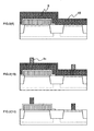
- Figs. 3(1) to 3(20) are a series of schematic cross-sectional views illustrating the steps of a conventional method of manufacturing a FLASHEEPROM.
- a first P-well 2 and a second P-well 3 are formed in a flash memory area and a logic area, respectively.
- a field oxide film 4 that defines areas of elements is formed, and thereafter an oxide film 5 with a thickness of 8 to 10 nm is formed on the surface of the substrate 1 by the thermal oxidation method (Fig. 3(1)).
- a first N - -type polysilicon 7 that is to become a FGE material in the flash memory area is formed thereon to a thickness of 150 nm.
- phosphorus is injected thereinto to a dopant concentration of approximately 1 to 3 ⁇ 10 19 atoms / cm 3 (Fig. 3(2)).
- a photoresist 6a is formed into the pattern (Fig. 3(3)) and, using this as a mask, etching is applied thereto (Fig. 3(4)).
- an ONO (Oxide-Nitride-Oxide) film 8 is grown over the entire surface to a thickness of 12 to 16 nm in terms of oxide film thickness by the CVD (Chemical Vapour Deposition) method (Fig. 3(5)).
- a photoresist 6b is then applied and patterned so as to cover only the flash memory area (Fig. 3(6)), and thereafter etching of said ONO film is performed.
- the oxide film 5 in the logic area is concurrently once removed (Fig. 3(7)), and a gate oxide film with a thickness of 5 nm, for example, is subsequently formed again in the logic area (Fig. 3(8)).
- a second polysilicon 9 that is to become a CGE material as well as a material for a gate electrode in the logic area is grown to a thickness of 200 nm (Fig. 3(9)).
- a photoresist 6c is formed into the pattern of electrodes of a memory-transistor and a select-transistor in the flash memory area, and formed over the entire surface, in the logic area (Fig. 3(10)).
- Etching is then applied to the second polysilicon 9 , the ONO film 8 in the flash memory area and the first polysilicon 7 (Fig. 3(11)).
- a first LDD (Lightly-Doped Drain) structure 11 in the flash memory area arsenic (As) or phosphorus (P) is ion-implanted thereinto with a dose of approximately 1 ⁇ 10 13 to 1 ⁇ 10 14 atoms / cm 2 .
- As arsenic
- P phosphorus
- the entire surface of the logic area is masked with a photoresist 6d (Fig. 3(12)).
- a photoresist 6e is formed into the pattern of the entire surface of the flash memory area and of the transistor of the logic area by means of patterning (Fig. 3(13)).
- the subsequent etching applied thereto forms a gate electrode of the transistor in the logic area (Fig. 3(14)).
- a second LDD 12 in the logic area the entire surface of the flash memory area is again covered with a photoresist 6f and, then, As or P is ion-implanted thereinto with a dose of approximately 1 ⁇ 10 13 to 1X10 14 atoms / cm 2 (Fig. 3 (15)).
- a titanium (Ti) film 15 is grown over the entire surface (Fig. 3(19)).
- silicide films 16 are selectively formed on the SD regions of the P-type substrate 1 as well as on the polysilicons of the transistors, and thereby a semiconductor device having a memory-transistor (Tr) and a select-transistor (Tr) in the flash memory area and a logic-transistor (Tr) in the logic area is accomplished (Fig. 3(20)).
- the first polysilicon 7 for the gate electrode of the select-transistor is not N + -type but N - -type so that holding characteristics of the flash memory does not become deteriorated.
- the use of N - -type brings about significant gate depletion, which results in an increase in effective thickness of the oxide film and a lowering of the operational speed.
- the first polysilicon 7 which is the gate electrode of the select-transistor is not turned to silicide and is insulated by the ONO film 8 from the second polysilicon 9 that is turned to silicide, the resistance thereof is considerable. This gives rise to a problem that the voltage applied substantially to the gate of the select-transistor varies from cell to cell and, therefore, the ON-current of the select-transistor varies with the cell.
- a select-transistor has a gate electrode formed in such a way that a silicon film either interposing a metal silicide film therebetween or having a silicide surface thereof is formed into the shape of a sidewall on the lateral face of a gate electrode of a memory-transistor, and an adjacent circuit transistor has a gate electrode formed from the same layer as said gate electrode of the select-transistor.
- JP-A-9-181282 there is disclosed a method of manufacturing a flash memory element, wherein, after a first polysilicon such as described above and an ONO film are formed, the ONO film lying in a select-transistor area and an adjacent circuit transistor area is removed by means of photolithography, and thereafter a second polysilicon is grown and, its surface being turned to silicide, patterning is applied thereto to form the shape of gate electrodes of a memory-transistor, a select-transistor and an adjacent circuit transistor, and then the ion implantation is carried out to form source-drain regions.
- the structure of the select-transistor is formed by patterning that is performed when a floating gate and a control gate of the select-transistor are directly contacted with each other. This produces an effect of lowering the gate resistance and, thus, making formation of a buttering contact as described above unnecessary.
- concentrations of the implanted dopants are different between the floating gate and the control gate, while they are in contact with each other, so that the depletion of the underlying floating gate cannot be eliminated thoroughly.
- the dopant concentration within a polysilicon layer is made uniform through thermal diffusion.
- the surface of the lower layer is exposed to the air during the step of forming the upper layer, which leads to the formation of a thin natural oxidation film. Though 1 to 2 nm thick at the most, this natural oxidation film makes the dopant diffusion still slower by its presence.
- the grain boundaries of polysilicon layers do not usually meet on the composition plane and this further hinders the dopant diffusion.
- the RTA (Rapid Thermal Annealing) treatment performed at 1020 °C for 10 seconds or so is sufficient for a single-layered polysilicon
- the RTA treatment at the same temperature must be carried out for as long as 40 seconds for a double-layered polysilicon such as the one described herein.
- to attain diffusion within the gate polysilicon in this instance while it takes 10 seconds in a single layer, it requires 40 seconds in a double layer. Consequently, in a transistor with a double-layered structure, the diffusion in the transverse direction within the LDD becomes more marked and the effective channel length, shorter. In short, the double layer is not suited for the miniaturization, because of its substantial short channel effect.
- an object of the present invention is to provide a nonvolatile memory semiconductor device having, on one and the same substrate, a flash memory area where a memory-transistor and a select-transistor are formed and a logic area where an adjacent circuit transistor is formed; which has a transistor structure capable to suppress the gate depletion particularly in the select-transistor and to perform high speed operations, all without making the steps of manufacturing method thereof unduly complicated.
- a gate electrode of the adjacent circuit transistor in the logic area is composed of a single layer of a polysilicon film, which is formed from the same layer as the floating gate of the memory-transistor and then doped to have an enhanced dopant concentration by ion implantation performed in the step of forming source-drain regions of the transistors.
- a gate electrode of the adjacent circuit transistor in the logic area is composed of a single layer being formed from the same layer as the control gate electrode of the memory-transistor.
- a method of manufacturing a nonvolatile memory semiconductor device having, on one and the same substrate, a flash memory area where a memory-transistor and a select-transistor are formed and a logic area where an adjacent circuit transistor is formed; which, at least, comprises the steps of:
- step (7) comprises the sub-steps of removing said nitride film as well as resist pattern and then performing the first ion implantation to form an LDD structure in the flash memory area, with another resist masking the entire surface of the logic area; removing the resist in the logic area and then performing the second ion implantation to form an LDD structure in the logic area, with another resist masking the entire surface of the flash memory area; and, in addition, forming sidewalls prior to another ion implantation to form source-drain regions.
- a method of manufacturing a nonvolatile memory semiconductor device having, on one and the same substrate, a flash memory area where a memory-transistor and a select-transistor are formed and a logic area where an adjacent circuit transistor is formed; which, at least, comprises the steps of:
- step (8) comprises the sub-steps of performing the first ion implantation to form an LDD structure in the flash memory area before removing said nitride film and resist pattern; removing said nitride film and resist and then performing the second ion implantation to form an LDD structure in the logic area, with another resist masking the entire surface of the flash memory area; and, in addition, forming sidewalls prior to another ion implantation to form flash memory area; and, in addition, forming sidewalls prior to another ion implantation to form source-drain regions.
- the gate electrode of the select-transistor produced in the flash memory area is composed of a single layer of a polysilicon film, which is formed from the same layer as the floating gate electrode of the memory-transistor and then doped to have an enhanced dopant concentration by ion implantation performed in the step of forming source-drain regions of the transistors, and therefore a select-transistor structure capable of high speed operations is provided. Furthermore, because of silicide formation on the gate surface of the select-transistor, the voltage applied substantially to the gate of the select-transistor becomes almost identical for every cell so that the problem associated with the conventional structure that the ON-current of the select-transistor varies with the cell is also eliminated.
- the present invention also has the effect of simplifying the steps thereof.
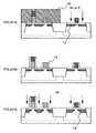
- Figs. 1(1) to 1(20) are a series of schematic cross-sectional views illustrating the steps of a method of manufacturing a FLASHEEPROM that is an embodiment of the present invention.
- a first P-well 2 and a second P-well 3 are formed in a flash memory area and a logic area, respectively.
- a field oxide film 4 that defines areas of elements is formed, and thereafter an oxide film 5 with a thickness of 6 to 8 nm is formed on the surface of the substrate 1 by the thermal oxidation method (Fig. 1(1)).
- the oxide film overlying the first P-well 2 is covered with a photoresist 6a , and then, after the oxide film overlying the second P-well 3 is once removed (Fig. 1(2)), a gate oxide film with a thickness of 5 nm is again formed by the thermal oxidation method (Fig. 1(3)).
- the film thickness of the oxide film in the flash memory area becomes 8 to 10 nm.
- a first N - -type polysilicon 7 that is to become a FGE material in the flash memory area is formed thereon to a thickness of 150 nm.
- phosphorus is injected thereinto to a dopant concentration of approximately 1 ⁇ 10 19 to 3 ⁇ 10 19 atoms / cm 3 (Fig. 1(4)).
- a photoresist 6b is formed into the pattern on the oxide film in the flash memory area and the logic area (Fig. 1(5)) and, using this as a mask, etching is applied thereto (Fig. 1(6)).
- an ONO film 8 is grown over the entire surface to a thickness of 12 to 16 nm in terms of oxide film thickness (Fig. 1(7)) and, over this, a second polysilicon 9 is grown to a thickness of 200 nm and then a nitride film 10 that is to serve as an etching mask for a floating gate in the later step is grown (Fig. 1(8)).
- a photoresist pattern 6 corresponding to the shape of an electrode of a memory-transistor in the flash memory area is formed on said nitride film 10 (Fig. 1(9)), and then the nitride film 10 , the second polysilicon 9 and the ONO film 8 are etched in succession (Fig. 1(10). After removing the photoresist, another resist pattern 6c is formed into the shape of a select-transistor gate and an adjacent circuit transistor gate (Fig. 1(11)).
- the first polysilicon 7 is etched (Fig. 1(12)).
- the nitride film as well as the resist are then removed (Fig. 1(13)), and thereafter, in order to form a first LDD structure 11 in the flash memory area, As or P is ion-implanted thereinto with a dose of approximately 1 ⁇ 10 13 to 1 ⁇ 10 14 atoms / cm 2 .
- the entire surface of the logic area is masked with a photoresist 6d (Fig. 1(14)).
- the resist formed in the logic area is removed and the entire surface of the flash memory area is again covered with a photoresist 6e and, then, As or P is ion-implanted thereinto with a dose of approximately 1 ⁇ 10 13 to 1 ⁇ 10 14 atoms/ cm 2 (Fig.1(15)).
- a photoresist 6e is ion-implanted thereinto with a dose of approximately 1 ⁇ 10 13 to 1 ⁇ 10 14 atoms/ cm 2 (Fig.1(15)).
- an oxide film is formed over the entire surface, and therefrom sidewalls 13 are formed on lateral faces of the electrode materials in the flash memory area and in the logic area (Fig. 1(16)).
- source-drain (SD) regions 14 in the flash memory area and in the logic area As is ion-implanted thereinto with a dose of approximately 1 ⁇ 10 15 to 5 ⁇ 10 15 atoms / cm 2 (Fig. 1 (17)).
- a titanium (Ti) film 15 is grown over the entire surface (Fig. 1(19)).
- silicide films 16 are selectively formed on the SD regions of the P-type substrate 1 as well as on the polysilicons of the transistors, and thereby a semiconductor device having a memory-transistor (Tr) and a select-transistor (Tr) in the flash memory area and a logic-transistor (Tr) in the logic area is accomplished (Fig. 1(20)).
- Figs. 2(1) to 2(20) are a series of schematic cross-sectional views illustrating the steps of a method of manufacturing a FLASHEEPROM that is another embodiment of the present invention.
- a first P-well 2 and a second P-well 3 are formed in a flash memory area and a logic area, respectively.
- a field oxide film 4 tat defines areas of elements is formed, and thereafter an oxide film 5 with a thickness of 8 to 10 nm is formed on the surface of the substrate 1 by the thermal oxidation method (Fig. 2(1)).
- a first N - -type polysilicon 7 that is to become a FGE material in the flash memory area is formed thereon to a thickness of 150 nm (Fig. 2(2)).
- the polysilicon film may be grown to a thickness of 150 nm by performing the CVD method using SiH 4 and PH 3 or AsH 3 , for example, as material gases and controlling the amount of the flow of the doping material so as to make the dopant concentration approximately 1 ⁇ 10 19 to 3 ⁇ 10 19 atoms / cm 3 .
- a photoresist 6a is formed into the pattern on the oxide film in the flash memory area (Fig. 2(3)), and, using this as a mask, etching is applied thereto (Fig. 2(4)).
- an ONO film 8 is grown over the entire surface to a thickness of 12 to 16 nm in terms of oxide film thickness (Fig. 2(5)).
- a photoresist 6b is formed into the pattern over the flash memory area and then etching is applied thereto (Fig. 2(6)).
- the oxide film on the surface of the substrate in the logic area is simultaneously removed (Fig. 2(7)) so that another oxide film (a gate oxide film) is subsequently formed again in the logic area by the thermal oxidation (Fig. 2(8)).
- a second polysilicon 9 is grown to a thickness of 200 nm and then a nitride film 10 that is to serve as an etching mask for the ONO film and a floating gate in the later step is grown (Fig. 2(9)).
- a photoresist pattern 6c corresponding to the shape of an electrode of a memory-transistor in the flash memory area and the shape of an adjacent circuit transistor in the logic area is formed on said nitride film 10 (Fig. 2(10)), and then the nitride film 10 and the second polysilicon 9 are etched in succession (Fig. 2(11).
- a second LDD 12 in the logic area the entire surface of the flash memory area is covered with a photoresist 6 and, then, As or P is ion-implanted thereinto with a dose of approximately 1 ⁇ 10 13 to 1 ⁇ 10 14 atoms / cm 2 (Fig. 2(15)).
- an oxide film is formed over the entire surface, and therefrom sidewalls 13 are formed on lateral faces of the electrode materials in the flash memory area and in the logic area (Fig. 2(16)).
- SD source-drain
- a titanium (Ti) film 15 is grown over the entire surface (Fig. 2(19)).
- silicide films 16 are selectively formed on the SD regions of the P-type substrate 1 as well as on the polysilicons of the transistors, and thereby a semiconductor device having a memory-transistor (Tr) and a select-transistor (Tr) in the flash memory area and a logic-transistor (Tr) in the logic area is accomplished (Fig. 2(20)).
- CMOS Complementary Metal-Oxide-Semiconductor
Abstract


Description
- The present invention relates to a semiconductor device and a manufacturing method thereof and more particularly to improvements in a gate electrode of a select-transistor in a 2-transistors type flash memory.
- An electrically-erasable nonvolatile semiconductor memory device such as a FLASHEEPROM (Flash Electrically-Erasable Programmable Read Only Memory) comprises two sorts of transistors, the memory-transistor and the select-transistor. A plurality of memory-transistors each of which has a floating gate electrode (FGE) and a control gate electrode (CGE) are formed in a memory cell area thereof and are under control as well as selection of a select-transistor. Further, in a more practically designed FLASHEEPROM, a transistor in a logic area such as the one in a logical operation circuit is also formed on the same substrate.
- For such a FLASHEEPROM as having a logic transistor on the same substrate, a gate electrode of the logic transistor and a CGE in the memory cell area are formed from the same layer in the manufacturing method generally used. Referring to the drawings, a conventional manufacturing method is described below.
- Figs. 3(1) to 3(20) are a series of schematic cross-sectional views illustrating the steps of a conventional method of manufacturing a FLASHEEPROM.
- First, upon a P-
type semiconductor substrate 1, a first P-well 2 and a second P-well 3 are formed in a flash memory area and a logic area, respectively. Next, a field oxide film 4 that defines areas of elements is formed, and thereafter anoxide film 5 with a thickness of 8 to 10 nm is formed on the surface of thesubstrate 1 by the thermal oxidation method (Fig. 3(1)). A first N--type polysilicon 7 that is to become a FGE material in the flash memory area is formed thereon to a thickness of 150 nm. After that, by means of ion implantation, phosphorus is injected thereinto to a dopant concentration of approximately 1 to 3 × 10¹⁹ atoms / cm3 (Fig. 3(2)). Next, in order to maintain said polysilicon only on the oxide film in the flash memory area, a photoresist 6a is formed into the pattern (Fig. 3(3)) and, using this as a mask, etching is applied thereto (Fig. 3(4)). - Next, covering said polysilicon, an ONO (Oxide-Nitride-Oxide)
film 8 is grown over the entire surface to a thickness of 12 to 16 nm in terms of oxide film thickness by the CVD (Chemical Vapour Deposition) method (Fig. 3(5)). Over that, a photoresist 6b is then applied and patterned so as to cover only the flash memory area (Fig. 3(6)), and thereafter etching of said ONO film is performed. At this, theoxide film 5 in the logic area is concurrently once removed (Fig. 3(7)), and a gate oxide film with a thickness of 5 nm, for example, is subsequently formed again in the logic area (Fig. 3(8)). - Over the entire surface of the substrate, a
second polysilicon 9 that is to become a CGE material as well as a material for a gate electrode in the logic area is grown to a thickness of 200 nm (Fig. 3(9)). Following that, on saidsecond polysilicon 9, a photoresist 6c is formed into the pattern of electrodes of a memory-transistor and a select-transistor in the flash memory area, and formed over the entire surface, in the logic area (Fig. 3(10)). Etching is then applied to thesecond polysilicon 9, theONO film 8 in the flash memory area and the first polysilicon 7 (Fig. 3(11)). - Next, in order to form a first LDD (Lightly-Doped Drain)
structure 11 in the flash memory area, arsenic (As) or phosphorus (P) is ion-implanted thereinto with a dose of approximately 1×10¹³ to 1×10¹⁴ atoms / cm2. For this, the entire surface of the logic area is masked with a photoresist 6d (Fig. 3(12)). After that, to form a logic-transistor, a photoresist 6e is formed into the pattern of the entire surface of the flash memory area and of the transistor of the logic area by means of patterning (Fig. 3(13)). The subsequent etching applied thereto forms a gate electrode of the transistor in the logic area (Fig. 3(14)). - Further, for the formation of a
second LDD 12 in the logic area, the entire surface of the flash memory area is again covered with a photoresist 6f and, then, As or P is ion-implanted thereinto with a dose of approximately 1×10¹³ to 1X10¹⁴ atoms / cm2 (Fig. 3 (15)). - After removing the photoresist, an oxide film is formed over the entire surface, and therefrom
sidewalls 13 are formed on lateral faces of the electrode materials in the flash memory area and in the logic area (Fig. 3(16)). Following that, to form source-drain (SD)regions 14 in the flash memory area and in the logic area, As is ion-implanted thereinto with a dose of approximately 1×10¹⁵ to 5×10¹⁵ atoms / cm2 (Fig. 3 (17)). - Next, the oxide film lying outside of the transistors is all removed by wet etching (Fig. 3(18)) and then a titanium (Ti)
film 15 is grown over the entire surface (Fig. 3(19)). Finally, by performing a salicide process in which titanium is turned to silicide and removing unreacted parts of theTi film 15 subsequently,silicide films 16 are selectively formed on the SD regions of the P-type substrate 1 as well as on the polysilicons of the transistors, and thereby a semiconductor device having a memory-transistor (Tr) and a select-transistor (Tr) in the flash memory area and a logic-transistor (Tr) in the logic area is accomplished (Fig. 3(20)). - In the flash memory formed in such a way as described above, the
first polysilicon 7 for the gate electrode of the select-transistor is not N+-type but N--type so that holding characteristics of the flash memory does not become deteriorated. The use of N--type, however, brings about significant gate depletion, which results in an increase in effective thickness of the oxide film and a lowering of the operational speed. Obviously with this manufacturing method, it is impossible to add the dopants to increase the dopant concentration in the first polysilicon 7 (to make it N+-type) so that the operational speed thereof cannot be improved further. Moreover, since thefirst polysilicon 7 which is the gate electrode of the select-transistor is not turned to silicide and is insulated by theONO film 8 from thesecond polysilicon 9 that is turned to silicide, the resistance thereof is considerable. This gives rise to a problem that the voltage applied substantially to the gate of the select-transistor varies from cell to cell and, therefore, the ON-current of the select-transistor varies with the cell. - It is reported that there have been an attempt to form a butting contact on an ONO film of a select-transistor so as to make electrical connection between the upper and the lower electrode layers. In this case, it is necessary to add the step of forming said contact into the manufacturing method thereof, which undoubtedly complicates the steps but its effect of reducing the gate resistance is not particularly promising so far.
- Meanwhile, in JP-A-5-121700, with the object of lowering the resistance of the select-transistor enough to achieve a higher operational speed, there is disclosed a structure in which a select-transistor has a gate electrode formed in such a way that a silicon film either interposing a metal silicide film therebetween or having a silicide surface thereof is formed into the shape of a sidewall on the lateral face of a gate electrode of a memory-transistor, and an adjacent circuit transistor has a gate electrode formed from the same layer as said gate electrode of the select-transistor.
- In the method described in said publication, however, conductive layers of polysilicon or the like must be formed twice for the formation of the gate electrode of the memory-transistor and once more for the formation of the select-transistor and the adjacent circuit transistor. Furthermore, there are problems that, because of an insulating film present between the select-transistor and the memory-transistor, no channel is formed under that insulating film and that the gate oxide film of the select-transistor becomes thicker than the gate oxide film of the memory-transistor, which inevitably hinders the improvement of the operational speed.
- Further, in JP-A-9-181282, there is disclosed a method of manufacturing a flash memory element, wherein, after a first polysilicon such as described above and an ONO film are formed, the ONO film lying in a select-transistor area and an adjacent circuit transistor area is removed by means of photolithography, and thereafter a second polysilicon is grown and, its surface being turned to silicide, patterning is applied thereto to form the shape of gate electrodes of a memory-transistor, a select-transistor and an adjacent circuit transistor, and then the ion implantation is carried out to form source-drain regions. In this method, the structure of the select-transistor is formed by patterning that is performed when a floating gate and a control gate of the select-transistor are directly contacted with each other. This produces an effect of lowering the gate resistance and, thus, making formation of a buttering contact as described above unnecessary.
- In this method, however, concentrations of the implanted dopants are different between the floating gate and the control gate, while they are in contact with each other, so that the depletion of the underlying floating gate cannot be eliminated thoroughly. In general, the dopant concentration within a polysilicon layer is made uniform through thermal diffusion. In the case that a polysilicon layer is laid over another polysilicon layer, however, the surface of the lower layer is exposed to the air during the step of forming the upper layer, which leads to the formation of a thin natural oxidation film. Though 1 to 2 nm thick at the most, this natural oxidation film makes the dopant diffusion still slower by its presence. In addition, when two layers of polysilicon are formed, the grain boundaries of polysilicon layers do not usually meet on the composition plane and this further hinders the dopant diffusion. For instance, if the RTA (Rapid Thermal Annealing) treatment performed at 1020 °C for 10 seconds or so is sufficient for a single-layered polysilicon, the RTA treatment at the same temperature must be carried out for as long as 40 seconds for a double-layered polysilicon such as the one described herein. In other words, to attain diffusion within the gate polysilicon in this instance, while it takes 10 seconds in a single layer, it requires 40 seconds in a double layer. Consequently, in a transistor with a double-layered structure, the diffusion in the transverse direction within the LDD becomes more marked and the effective channel length, shorter. In short, the double layer is not suited for the miniaturization, because of its substantial short channel effect.
- Further, since the step of another photolithography is added to remove the ONO film lying in the select-transistor area and the adjacent circuit transistor area, another problem of further complicating steps also arises for this method.
- Accordingly, an object of the present invention is to provide a nonvolatile memory semiconductor device having, on one and the same substrate, a flash memory area where a memory-transistor and a select-transistor are formed and a logic area where an adjacent circuit transistor is formed; which has a transistor structure capable to suppress the gate depletion particularly in the select-transistor and to perform high speed operations, all without making the steps of manufacturing method thereof unduly complicated.
- In accordance with the present invention, there are presented the following structures and manufacturing methods thereof:
- A nonvolatile memory semiconductor device having, on one and the same substrate, a flash memory area where a memory-transistor and a select-transistor are formed and a logic area where an adjacent circuit transistor is formed; wherein:
- said memory-transistor is composed of layers of structure consisting of a floating gate and a control gate separated by a first insulating film; and
- at least, a gate electrode of the select-transistor is composed of a single layer of a polysilicon film, which is formed from the same layer as the floating gate of the memory-transistor and then doped to have an enhanced dopant concentration by ion implantation performed in the step of forming source-drain regions of the transistors.
-
- The afore-mentioned semiconductor device, wherein a gate electrode of the adjacent circuit transistor in the logic area is composed of a single layer of a polysilicon film, which is formed from the same layer as the floating gate of the memory-transistor and then doped to have an enhanced dopant concentration by ion implantation performed in the step of forming source-drain regions of the transistors.
- The afore-mentioned semiconductor device, wherein a gate electrode of the adjacent circuit transistor in the logic area is composed of a single layer being formed from the same layer as the control gate electrode of the memory-transistor.
- The afore-mentioned semiconductor device, wherein the surface of the control gate of the memory-transistor and the surfaces of the gate electrodes of the select-transistor and of the adjacent circuit transistor in the logic area have undergone the chemical change to silicide.
- The afore-mentioned semiconductor device, wherein a sidewall is formed on each lateral face of the gate electrode of each transistor and an LDD structure is each formed in the substrate under said sidewall.
- A method of manufacturing a nonvolatile memory semiconductor device having, on one and the same substrate, a flash memory area where a memory-transistor and a select-transistor are formed and a logic area where an adjacent circuit transistor is formed; which, at least, comprises the steps of:
- (1) growing an N--type first polysilicon upon a semiconductor substrate on which an element isolation region and an oxide film are formed;
- (2) removing the first polysilicon overlying the element isolation region by etching;
- (3) growing a first insulating film over the entire surface so as to cover the remaining first polysilicon;
- (4) growing a second polysilicon as well as a nitride film over the entire surface;
- (5) forming a resist pattern at the position where electrodes of the memory-transistor are to be formed and, then, with said pattern used as a mask, carrying out etching of the nitride film, the second polysilicon and the first polysilicon;
- (6) removing the resist pattern, and thereafter forming another resist pattern at the positions where electrodes of the select-transistor and the adjacent circuit transistor are to be formed and, then, with said nitride film used as a mask for the memory-transistor and said pattern, for the select-transistor and the adjacent circuit transistor, carrying out etching of the first polysilicon;
- (7) removing said nitride film as well as said resist pattern, and thereafter, concurrently with forming source-drain regions, applying ion implantation to the second polysilicon which is to serve as a control gate of the memory-transistor and to the first polysilicon which is to serve as gate electrodes of the select-transistor and of the adjacent circuit transistor in the logic area; and
- (8) removing, by means of isotropic etching, the oxide film lying on the substrate surface other than the parts thereof underlying every transistor, to the level where the substrate surface is exposed. The afore-mentioned method of manufacturing a semiconductor device, which further comprises the step of injecting dopants by ion implantation after growing said N--type first polysilicon.The afore-mentioned method of manufacturing a semiconductor device, which, after said step (8), further comprises the step of:
- (9) growing a metal film over the entire surface for the silicide formation, and thereafter subjecting that to the chemical change to silicide and then removing the unreacted metal film.
-
- The afore-mentioned method of manufacturing a semiconductor device, wherein said step (7) comprises the sub-steps of removing said nitride film as well as resist pattern and then performing the first ion implantation to form an LDD structure in the flash memory area, with another resist masking the entire surface of the logic area; removing the resist in the logic area and then performing the second ion implantation to form an LDD structure in the logic area, with another resist masking the entire surface of the flash memory area; and, in addition, forming sidewalls prior to another ion implantation to form source-drain regions.
- A method of manufacturing a nonvolatile memory semiconductor device having, on one and the same substrate, a flash memory area where a memory-transistor and a select-transistor are formed and a logic area where an adjacent circuit transistor is formed; which, at least, comprises the steps of:
- (1) growing an N--type first polysilicon upon a semiconductor substrate on which an element isolation region and an oxide film are formed;
- (2) removing the first polysilicon overlying the element isolation region as well as the logic area by etching;
- (3) growing a first insulating film over the entire surface so as to cover the remaining first polysilicon;
- (4) removing, at least, the first insulating film in the logic area;
- (5) growing a second polysilicon as well as a nitride film over the entire surface;
- (6) forming a resist pattern at the positions where electrodes of the memory-transistor and the adjacent circuit transistor are to be formed and, then, with said pattern used as a mask, carrying out etching of the nitride film and the second polysilicon;
- (7) removing the resist pattern, and thereafter forming another resist pattern at the position where an electrode of the select-transistor is to be formed as well as on the entire surface of the logic area, and, then, with said nitride film used as a mask for the memory-transistor and said pattern, for the select-transistor, carrying out etching of the first insulating film and the first polysilicon;
- (8) removing said nitride film as well as said resist pattern, and thereafter, concurrently with forming source-drain regions, applying ion implantation to the second polysilicon which is to serve as a control gate of the memory-transistor and as a gate electrode of the adjacent circuit transistor in the logic area and to the first polysilicon which is to serve as a gate electrode of the select-transistor; and
- (9) removing, by means of isotropic etching, the oxide film lying on the substrate surface other than the parts thereof underlying every transistor, to the level where the substrate surface is exposed. The afore-mentioned method of manufacturing a semiconductor device, which further comprises the step of injecting dopants by ion implantation after growing said N--type first polysilicon.The afore-mentioned method of manufacturing a semiconductor device, which, after said step (9), further comprises the step of:
- (10) growing a metal film over the entire surface for the suicide formation, and thereafter subjecting that to the chemical change to suicide and then removing the unreacted metal film.
-
- The afore-mentioned method of manufacturing a semiconductor device, wherein said step (8) comprises the sub-steps of performing the first ion implantation to form an LDD structure in the flash memory area before removing said nitride film and resist pattern; removing said nitride film and resist and then performing the second ion implantation to form an LDD structure in the logic area, with another resist masking the entire surface of the flash memory area; and, in addition, forming sidewalls prior to another ion implantation to form flash memory area; and, in addition, forming sidewalls prior to another ion implantation to form source-drain regions.
- According to the present invention, the gate electrode of the select-transistor produced in the flash memory area is composed of a single layer of a polysilicon film, which is formed from the same layer as the floating gate electrode of the memory-transistor and then doped to have an enhanced dopant concentration by ion implantation performed in the step of forming source-drain regions of the transistors, and therefore a select-transistor structure capable of high speed operations is provided. Furthermore, because of silicide formation on the gate surface of the select-transistor, the voltage applied substantially to the gate of the select-transistor becomes almost identical for every cell so that the problem associated with the conventional structure that the ON-current of the select-transistor varies with the cell is also eliminated.
- Further, in the manufacturing method of the present invention, a simple addition of the step of forming a nitride film over the second polysilicon makes it unnecessary to add the step of troublesome photolithography which is required, in the conventional method, to perform in the later step, in removing the ONO film lying outside of the memory transistor area, thus, the present invention also has the effect of simplifying the steps thereof.
-
- Figs. 1(1) to 1(20) are a series of schematic cross-sectional views illustrating the steps of a method of manufacturing a FLASHEEPROM that is an embodiment of the present invention.
- Figs. 2(1) to 2(20) are a series of schematic cross-sectional views illustrating the steps of a method of manufacturing a FLASHEEPROM that is another embodiment of the present invention.
- Figs. 3(1) to 3(20) are a series of schematic cross-sectional views illustrating the steps of a conventional method of manufacturing a FLASHEEPROM.
-
- Referring to the drawings, the present invention is described in detail below.
- Figs. 1(1) to 1(20) are a series of schematic cross-sectional views illustrating the steps of a method of manufacturing a FLASHEEPROM that is an embodiment of the present invention.
- First, upon a P-
type semiconductor substrate 1, a first P-well 2 and a second P-well 3 are formed in a flash memory area and a logic area, respectively. Next, a field oxide film 4 that defines areas of elements is formed, and thereafter anoxide film 5 with a thickness of 6 to 8 nm is formed on the surface of thesubstrate 1 by the thermal oxidation method (Fig. 1(1)). Next, the oxide film overlying the first P-well 2 is covered with aphotoresist 6a, and then, after the oxide film overlying the second P-well 3 is once removed (Fig. 1(2)), a gate oxide film with a thickness of 5 nm is again formed by the thermal oxidation method (Fig. 1(3)). Through that, the film thickness of the oxide film in the flash memory area becomes 8 to 10 nm. A first N--type polysilicon 7 that is to become a FGE material in the flash memory area is formed thereon to a thickness of 150 nm. After that, by means of ion implantation, phosphorus is injected thereinto to a dopant concentration of approximately 1 × 10¹⁹ to 3 × 10¹⁹ atoms / cm3 (Fig. 1(4)). - Next, in order to remove said
first polysilicon film 7 above theelement isolation region 2, aphotoresist 6b is formed into the pattern on the oxide film in the flash memory area and the logic area (Fig. 1(5)) and, using this as a mask, etching is applied thereto (Fig. 1(6)). Next, covering remaining said polysilicon, anONO film 8 is grown over the entire surface to a thickness of 12 to 16 nm in terms of oxide film thickness (Fig. 1(7)) and, over this, asecond polysilicon 9 is grown to a thickness of 200 nm and then anitride film 10 that is to serve as an etching mask for a floating gate in the later step is grown (Fig. 1(8)). - Following that, a photoresist pattern 6 corresponding to the shape of an electrode of a memory-transistor in the flash memory area is formed on said nitride film 10 (Fig. 1(9)), and then the
nitride film 10, thesecond polysilicon 9 and theONO film 8 are etched in succession (Fig. 1(10). After removing the photoresist, another resistpattern 6c is formed into the shape of a select-transistor gate and an adjacent circuit transistor gate (Fig. 1(11)). - Next, using as a mask said nitride film in the memory-transistor area and the resist pattern, in the other areas, the
first polysilicon 7 is etched (Fig. 1(12)). The nitride film as well as the resist are then removed (Fig. 1(13)), and thereafter, in order to form afirst LDD structure 11 in the flash memory area, As or P is ion-implanted thereinto with a dose of approximately 1×10¹³ to 1×10¹⁴ atoms / cm2. For this, the entire surface of the logic area is masked with aphotoresist 6d (Fig. 1(14)). - Next, for the formation of a
second LDD 12 in the logic area, the resist formed in the logic area is removed and the entire surface of the flash memory area is again covered with aphotoresist 6e and, then, As or P is ion-implanted thereinto with a dose of approximately 1×10¹³ to 1×10¹⁴ atoms/ cm2 (Fig.1(15)). After removing the photoresist, an oxide film is formed over the entire surface, and therefromsidewalls 13 are formed on lateral faces of the electrode materials in the flash memory area and in the logic area (Fig. 1(16)). Following that, to form source-drain (SD)regions 14 in the flash memory area and in the logic area, As is ion-implanted thereinto with a dose of approximately 1×10¹⁵ to 5×10¹⁵ atoms / cm2 (Fig. 1 (17)). - Next, the oxide film lying outside of the transistors is all removed by wet etching (Fig. 1(18)) and then a titanium (Ti)
film 15 is grown over the entire surface (Fig. 1(19)). Finally, by performing a salicide process in which titanium is turned to silicide and removing unreacted parts of theTi film 15 subsequently,silicide films 16 are selectively formed on the SD regions of the P-type substrate 1 as well as on the polysilicons of the transistors, and thereby a semiconductor device having a memory-transistor (Tr) and a select-transistor (Tr) in the flash memory area and a logic-transistor (Tr) in the logic area is accomplished (Fig. 1(20)). - Figs. 2(1) to 2(20) are a series of schematic cross-sectional views illustrating the steps of a method of manufacturing a FLASHEEPROM that is another embodiment of the present invention.
- First, upon a P-
type semiconductor substrate 1, a first P-well 2 and a second P-well 3 are formed in a flash memory area and a logic area, respectively. Next, a field oxide film 4 tat defines areas of elements is formed, and thereafter anoxide film 5 with a thickness of 8 to 10 nm is formed on the surface of thesubstrate 1 by the thermal oxidation method (Fig. 2(1)). Next, a first N--type polysilicon 7 that is to become a FGE material in the flash memory area is formed thereon to a thickness of 150 nm (Fig. 2(2)). Alternatively, the polysilicon film may be grown to a thickness of 150 nm by performing the CVD method using SiH4 and PH3 or AsH3, for example, as material gases and controlling the amount of the flow of the doping material so as to make the dopant concentration approximately 1×10¹⁹ to 3×10¹⁹ atoms / cm3. Next, in order to remove saidfirst polysilicon film 7 lying outside of the flash memory area, aphotoresist 6a is formed into the pattern on the oxide film in the flash memory area (Fig. 2(3)), and, using this as a mask, etching is applied thereto (Fig. 2(4)). - Next, covering remaining said polysilicon, an
ONO film 8 is grown over the entire surface to a thickness of 12 to 16 nm in terms of oxide film thickness (Fig. 2(5)). To remove the ONO film in the logic area, aphotoresist 6b is formed into the pattern over the flash memory area and then etching is applied thereto (Fig. 2(6)). At this, the oxide film on the surface of the substrate in the logic area is simultaneously removed (Fig. 2(7)) so that another oxide film (a gate oxide film) is subsequently formed again in the logic area by the thermal oxidation (Fig. 2(8)). - Over this, a
second polysilicon 9 is grown to a thickness of 200 nm and then anitride film 10 that is to serve as an etching mask for the ONO film and a floating gate in the later step is grown (Fig. 2(9)). Following that, aphotoresist pattern 6c corresponding to the shape of an electrode of a memory-transistor in the flash memory area and the shape of an adjacent circuit transistor in the logic area is formed on said nitride film 10 (Fig. 2(10)), and then thenitride film 10 and thesecond polysilicon 9 are etched in succession (Fig. 2(11). - After removing the photoresist, another resist
pattern 6d is formed into the shape of a select-transistor gate as well as on the entire surface of the logic area. Then, using as a mask said nitride film in the memory-transistor area and the resist pattern, in the select-transistor area, theONO film 8 and thefirst polysilicon 7 in the flash memory area are etched (Fig. 2(12)). Leaving the nitride film and the resist as they are, As or P is ion-implanted thereinto with a dose of 1×10¹³ to 1×10¹⁴ atoms / cm2, in order to form afirst LDD structure 11 in the flash memory area (Fig. 2(13)). After that, the photoresist, the ONO film lying on the gate of the select-transistor and finally the nitride film are removed in succession (Fig. 2(14)). - Next, for the formation of a
second LDD 12 in the logic area, the entire surface of the flash memory area is covered with a photoresist 6 and, then, As or P is ion-implanted thereinto with a dose of approximately 1×10¹³ to 1×10¹⁴ atoms / cm2 (Fig. 2(15)). After removing the photoresist, an oxide film is formed over the entire surface, and therefromsidewalls 13 are formed on lateral faces of the electrode materials in the flash memory area and in the logic area (Fig. 2(16)). Following that, to form source-drain (SD)regions 14 in the flash memory area and in the logic area, As is ion-implanted thereinto with a dose of approximately 1×10¹⁵ atoms / cm2 (Fig. 2 (17)). - Next, the oxide film lying outside of the transistors is all removed by wet etching (Fig. 2(18)) and then a titanium (Ti)
film 15 is grown over the entire surface (Fig. 2(19)). Finally, by performing a salicide process in which titanium is turned to silicide and removing unreacted parts of theTi film 15 subsequently,silicide films 16 are selectively formed on the SD regions of the P-type substrate 1 as well as on the polysilicons of the transistors, and thereby a semiconductor device having a memory-transistor (Tr) and a select-transistor (Tr) in the flash memory area and a logic-transistor (Tr) in the logic area is accomplished (Fig. 2(20)). - Further, while, in the above description, a semiconductor device having an N-channel structure is taken as an example, it is to be understood that the present invention may be applied to the one having a P-channel structure or a CMOS (Complementary Metal-Oxide-Semiconductor) structure.
| Explanation of symbols: | |
| 1: P-type substrate; | 2: First P-well; |
| 3: Second P-well; | 4: Field oxide film; |
| 5: Oxide film; | 6: Photoresist; |
| 7: First polysilicon (N-); | 8: ONO film; |
| 9: Second polysilicon; | 10: Nitride film; |
| 11: First LDD; | 12: Second LDD; |
| 13: Sidewall; | 14: SD region; |
| 15: Titanium film; | 16: Silicide film. |
Claims (13)
- A nonvolatile memory semiconductor device having, on one and the same substrate, a flash memory area where a memory-transistor and a select-transistor are formed and a logic area where an adjacent circuit transistor is formed; wherein:said memory-transistor is composed of layers of structure consisting of a floating gate and a control gate separated by a first insulating film; andat least, a gate electrode of the select-transistor is composed of a single layer of a polysilicon film, which is formed from the same layer as the floating gate of the memory-transistor and then doped to have an enhanced dopant concentration by ion implantation performed in the step of forming source-drain regions of the transistors.
- The semiconductor device according to Claim 1, wherein a gate electrode of the adjacent circuit transistor in the logic area is composed of a single layer of a polysilicon film, which is formed from the same layer as the floating gate of the memory-transistor and then doped to have an enhanced dopant concentration by ion implantation performed in the step of forming source-drain regions of the transistors.
- The semiconductor device according to Claim 1, wherein a gate electrode of the adjacent circuit transistor in the logic area is composed of a single layer being formed from the same layer as the control gate of the memory-transistor.
- The semiconductor device according to one of Claims 1 to 3 wherein the surface of the control gate of the memory-transistor and the surfaces of the gate electrodes of the select-transistor and of the adjacent circuit transistor in the logic area have undergone the chemical change to silicide.
- The semiconductor device according to one of Claims 1 to 4, wherein a sidewall is formed on each lateral face of the gate electrode of each transistor and an LDD structure is each formed in the substrate under said sidewall.
- A method of manufacturing a nonvolatile memory semiconductor device having, on one and the same substrate, a flash memory area where a memory-transistor and a select-transistor are formed and a logic area where an adjacent circuit transistor is formed; which, at least, comprises the steps of:(1) growing an N--type first polysilicon upon a semiconductor substrate on which an element isolation region and an oxide film are formed;(2) removing the first polysilicon overlying the element isolation region by etching;(3) growing a first insulating film over the entire surface so as to cover the remaining first polysilicon;(4) growing a second polysilicon as well as a nitride film over the entire surface;(5) forming a resist pattern at the position where electrodes of the memory-transistor are to be formed and, then, with said pattern used as a mask, carrying out etching of the nitride film, the second polysilicon and the first polysilicon;(6) removing the resist pattern, and thereafter forming another resist pattern at the positions where electrodes of the select-transistor and the adjacent circuit transistor are to be formed and, then, with said nitride film used as a mask for the memory-transistor and said pattern, for the select-transistor and the adjacent circuit transistor, carrying out etching of the first polysilicon;(7) removing said nitride film as well as said resist pattern, and thereafter, concurrently with forming source-drain regions, applying ion implantation to the second polysilicon which is to serve as a control gate of the memory-transistor and to the first polysilicon which is to serve as gate electrodes of the select-transistor and of the adjacent circuit transistor in the logic area; and(8) removing, by means of isotropic etching, the oxide film lying on the substrate surface other than the parts thereof underlying every transistor, to the level where the substrate surface is exposed.
- The method of manufacturing a semiconductor device according to Claim 6, which further comprises the step of injecting dopants by ion implantation after growing said N--type first polysilicon.
- The method of manufacturing a semiconductor device according to Claim 6 or 7, which, after said step (8), further comprises the step of:(9) growing a metal film over the entire surface for the silicide formation, and thereafter subjecting that to the chemical change to silicide and then removing the unreacted metal film.
- The method of manufacturing a semiconductor device according to one of Claims 6 to 8, wherein said step (7) comprises the sub-steps of removing said nitride film as well as resist pattern and then performing the first ion implantation to form an LDD structure in the flash memory area, with another resist masking the entire surface of the logic area; removing the resist in the logic area and then performing the second ion implantation to form an LDD structure in the logic area, with another resist masking the entire surface of the flash memory area; and, in addition, forming sidewalls prior to another ion implantation to form source-drain regions.
- A method of manufacturing a nonvolatile memory semiconductor device having, on one and the same substrate, a flash memory area where a memory-transistor and a select-transistor are formed and a logic area where an adjacent circuit transistor is formed; which, at least, comprises the steps of:(1) growing an N--type first polysilicon upon a semiconductor substrate on which an element isolation region and an oxide film are formed;(2) removing the first polysilicon overlying the element isolation region as well as the logic area by etching;(3) growing a first insulating film over the entire surface so as to cover the remaining first polysilicon;(4) removing, at least, the first insulating film in the logic area;(5) growing a second polysilicon as well as a nitride film over the entire surface;(6) forming a resist pattern at the positions where electrodes of the memory-transistor and the adjacent circuit transistor are to be formed and, then, with said pattern used as a mask, carrying out etching of the nitride film and the second polysilicon;(7) removing the resist pattern, and thereafter forming another resist pattern at the position where an electrode of the select-transistor is to be formed as well as on the entire surface of the logic area, and, then, with said nitride film used as a mask for the memory-transistor and said pattern, for the select-transistor, carrying out etching of the first insulating film and the first polysilicon;(8) removing said nitride film as well as said resist pattern, and thereafter, concurrently with forming source-drain regions, applying ion implantation to the second polysilicon which is to serve as a control gate of the memory-transistor and as a gate electrode of the adjacent circuit transistor in the logic area and to the first polysilicon which is to serve as a gate electrode of the select-transistor; and(9) removing, by means of isotropic etching, the oxide film lying on the substrate surface other than the parts thereof underlying every transistor, to the level where the substrate surface is exposed.
- The method of manufacturing a semiconductor device according to Claim 10, which further comprises the step of injecting dopants by ion implantation after growing said N--type first polysilicon.
- The method of manufacturing a semiconductor device according to Claim 10 or 11, which, after said step (9), further comprises the step of:(10) growing a metal film over the entire surface for the silicide formation, and thereafter subjecting that to the chemical change to silicide and then removing the unreacted metal film.
- The method of manufacturing a semiconductor device according to Claim 10, 11 or 12, wherein said step (8) comprises the sub-steps of removing said nitride film as well as resist pattern and then performing the first ion implantation to form an LDD structure in the flash memory area, with another resist masking the entire surface of the logic area; removing the resist in the logic area and then performing the second ion implantation to form an LDD structure in the logic area, with another resist masking the entire surface of the flash memory area; and, in addition, forming sidewalls prior to another ion implantation to form source-drain regions.
Applications Claiming Priority (2)
| Application Number | Priority Date | Filing Date | Title |
|---|---|---|---|
| JP33583598A JP3314807B2 (en) | 1998-11-26 | 1998-11-26 | Method for manufacturing semiconductor device |
| JP33583598 | 1998-11-26 |
Publications (2)
| Publication Number | Publication Date |
|---|---|
| EP1005081A2 true EP1005081A2 (en) | 2000-05-31 |
| EP1005081A3 EP1005081A3 (en) | 2001-02-07 |
Family
ID=18292945
Family Applications (1)
| Application Number | Title | Priority Date | Filing Date |
|---|---|---|---|
| EP99123440A Withdrawn EP1005081A3 (en) | 1998-11-26 | 1999-11-24 | Semiconductor nonvolatile memory and manufacturing method thereof |
Country Status (4)
| Country | Link |
|---|---|
| US (2) | US6287907B1 (en) |
| EP (1) | EP1005081A3 (en) |
| JP (1) | JP3314807B2 (en) |
| KR (1) | KR100392532B1 (en) |
Cited By (2)
| Publication number | Priority date | Publication date | Assignee | Title |
|---|---|---|---|---|
| EP1962332A2 (en) | 2007-02-22 | 2008-08-27 | Fujitsu Ltd. | Semiconductor device and method for manufacturing the same |
| EP1494276A3 (en) * | 2003-06-30 | 2009-06-24 | Kabushiki Kaisha Toshiba | Semiconductor device including nonvolatile memory and method for fabricating the same |
Families Citing this family (23)
| Publication number | Priority date | Publication date | Assignee | Title |
|---|---|---|---|---|
| JP2003518742A (en) * | 1999-12-21 | 2003-06-10 | コーニンクレッカ フィリップス エレクトロニクス エヌ ヴィ | Non-volatile memory cells and peripherals |
| JP4078014B2 (en) * | 2000-05-26 | 2008-04-23 | 株式会社ルネサステクノロジ | Nonvolatile semiconductor memory device and manufacturing method thereof |
| JP2002064157A (en) * | 2000-06-09 | 2002-02-28 | Toshiba Corp | Semiconductor memory integrated circuit and its manufacturing method |
| JP2002050697A (en) * | 2000-08-07 | 2002-02-15 | Mitsubishi Electric Corp | Method for manufacturing semiconductor device and the semiconductor device |
| JP2002151686A (en) * | 2000-11-15 | 2002-05-24 | Nec Corp | Semiconductor device and manufacturing method thereof |
| US6338992B1 (en) * | 2000-11-29 | 2002-01-15 | Lsi Logic Corporation | Programmable read only memory in CMOS process flow |
| US6429067B1 (en) * | 2001-01-17 | 2002-08-06 | International Business Machines Corporation | Dual mask process for semiconductor devices |
| KR100549320B1 (en) * | 2002-02-21 | 2006-02-02 | 마츠시타 덴끼 산교 가부시키가이샤 | Semiconductor storage device and its manufacturing method |
| KR20030085631A (en) * | 2002-04-29 | 2003-11-07 | 주식회사 하이닉스반도체 | Method of fabricating semiconductor devices |
| JP5179692B2 (en) * | 2002-08-30 | 2013-04-10 | 富士通セミコンダクター株式会社 | Semiconductor memory device and manufacturing method thereof |
| US7256090B2 (en) * | 2003-12-31 | 2007-08-14 | Dongbu Electronics Co., Ltd. | Method for fabricating semiconductor device |
| KR100655285B1 (en) | 2004-11-04 | 2006-12-08 | 삼성전자주식회사 | Semiconductor device having stack gate and method of fabricating the same |
| CN100361292C (en) * | 2004-12-30 | 2008-01-09 | 旺宏电子股份有限公司 | Quickflashing memory unit manufacturing method |
| CN100442524C (en) * | 2005-09-28 | 2008-12-10 | 中芯国际集成电路制造(上海)有限公司 | Structure and method for disposable programmable memory for built-in EEPROM |
| JP5118341B2 (en) * | 2006-12-22 | 2013-01-16 | 株式会社東芝 | Semiconductor memory device and manufacturing method thereof |
| US7652923B2 (en) * | 2007-02-02 | 2010-01-26 | Macronix International Co., Ltd. | Semiconductor device and memory and method of operating thereof |
| KR101001466B1 (en) * | 2007-03-06 | 2010-12-14 | 주식회사 하이닉스반도체 | Method of manufacturing a non-volatile memory device |
| JP5546740B2 (en) | 2008-05-23 | 2014-07-09 | ローム株式会社 | Semiconductor device |
| US8228726B2 (en) * | 2008-12-14 | 2012-07-24 | Chip Memory Technology, Inc. | N-channel SONOS non-volatile memory for embedded in logic |
| CN101777562B (en) * | 2010-01-15 | 2015-05-20 | 复旦大学 | Non-volatile semiconductor memory with floating gate and manufacturing method thereof |
| CN101800251B (en) * | 2010-01-29 | 2015-04-15 | 复旦大学 | Electric charge capture non-volatile semiconductor storage unit and manufacture method thereof |
| JP6065586B2 (en) | 2012-12-28 | 2017-01-25 | 日亜化学工業株式会社 | Light emitting device and manufacturing method thereof |
| CN104425366B (en) * | 2013-08-20 | 2017-12-29 | 中芯国际集成电路制造(北京)有限公司 | The forming method of semiconductor structure |
Citations (6)
| Publication number | Priority date | Publication date | Assignee | Title |
|---|---|---|---|---|
| EP0395084A2 (en) * | 1989-04-28 | 1990-10-31 | Kabushiki Kaisha Toshiba | Method of manufacturing a logic semiconductor device having non-volatile memory |
| US5066992A (en) * | 1989-06-23 | 1991-11-19 | Atmel Corporation | Programmable and erasable MOS memory device |
| US5235200A (en) * | 1990-01-29 | 1993-08-10 | Hitachi, Ltd. | Semiconductor integrated circuit device |
| JPH0855920A (en) * | 1994-08-15 | 1996-02-27 | Toshiba Corp | Manufacture of semiconductor device |
| US5497018A (en) * | 1991-11-14 | 1996-03-05 | Fujitsu Limited | Semiconductor memory device having a floating gate with improved insulation film quality |
| JPH0870055A (en) * | 1994-08-30 | 1996-03-12 | Nkk Corp | Manufacture of nonvolatile semiconductor storage device |
Family Cites Families (16)
| Publication number | Priority date | Publication date | Assignee | Title |
|---|---|---|---|---|
| JPH07114264B2 (en) * | 1985-08-23 | 1995-12-06 | 株式会社日立製作所 | Method for manufacturing semiconductor integrated circuit device |
| JPH03125479A (en) | 1989-10-11 | 1991-05-28 | Kawasaki Steel Corp | Manufacture of semiconductor integration circuit with non-volatile memory element |
| JPH088314B2 (en) | 1989-10-11 | 1996-01-29 | 株式会社東芝 | Nonvolatile semiconductor memory device and manufacturing method thereof |
| JPH05121700A (en) | 1991-08-28 | 1993-05-18 | Fujitsu Ltd | Semiconductor device and its manufacture |
| US5273923A (en) * | 1991-10-09 | 1993-12-28 | Motorola, Inc. | Process for fabricating an EEPROM cell having a tunnel opening which overlaps field isolation regions |
| JPH08139089A (en) | 1994-11-08 | 1996-05-31 | Sony Corp | Semiconductor device |
| JPH08148586A (en) * | 1994-11-21 | 1996-06-07 | Toshiba Corp | Manufacture of semiconductor device |
| JPH08167705A (en) * | 1994-12-15 | 1996-06-25 | Toshiba Corp | Nonvolatile semiconductor memory and manufacture thereof |
| US6475846B1 (en) * | 1995-05-18 | 2002-11-05 | Texas Instruments Incorporated | Method of making floating-gate memory-cell array with digital logic transistors |
| JPH0955441A (en) | 1995-08-10 | 1997-02-25 | Sony Corp | Manufacture of semiconductor device |
| KR970053947A (en) | 1995-12-16 | 1997-07-31 | 김광호 | Nonvolatile semiconductor memory device and manufacturing method thereof |
| JPH09283643A (en) * | 1996-04-19 | 1997-10-31 | Rohm Co Ltd | Semiconductor device and manufacture of semiconductor device |
| US5668035A (en) * | 1996-06-10 | 1997-09-16 | Taiwan Semiconductor Manufacturing Company Ltd. | Method for fabricating a dual-gate dielectric module for memory with embedded logic technology |
| JPH10270578A (en) | 1997-03-27 | 1998-10-09 | Seiko Instr Inc | Semiconductor device and manufacture thereof |
| JP3586072B2 (en) * | 1997-07-10 | 2004-11-10 | 株式会社東芝 | Nonvolatile semiconductor memory device |
| US6037222A (en) * | 1998-05-22 | 2000-03-14 | Taiwan Semiconductor Manufacturing Company | Method for fabricating a dual-gate dielectric module for memory embedded logic using salicide technology and polycide technology |
-
1998
- 1998-11-26 JP JP33583598A patent/JP3314807B2/en not_active Expired - Fee Related
-
1999
- 1999-11-23 US US09/447,869 patent/US6287907B1/en not_active Expired - Fee Related
- 1999-11-24 KR KR10-1999-0052429A patent/KR100392532B1/en not_active IP Right Cessation
- 1999-11-24 EP EP99123440A patent/EP1005081A3/en not_active Withdrawn
-
2001
- 2001-09-12 US US09/950,870 patent/US6534355B2/en not_active Expired - Fee Related
Patent Citations (6)
| Publication number | Priority date | Publication date | Assignee | Title |
|---|---|---|---|---|
| EP0395084A2 (en) * | 1989-04-28 | 1990-10-31 | Kabushiki Kaisha Toshiba | Method of manufacturing a logic semiconductor device having non-volatile memory |
| US5066992A (en) * | 1989-06-23 | 1991-11-19 | Atmel Corporation | Programmable and erasable MOS memory device |
| US5235200A (en) * | 1990-01-29 | 1993-08-10 | Hitachi, Ltd. | Semiconductor integrated circuit device |
| US5497018A (en) * | 1991-11-14 | 1996-03-05 | Fujitsu Limited | Semiconductor memory device having a floating gate with improved insulation film quality |
| JPH0855920A (en) * | 1994-08-15 | 1996-02-27 | Toshiba Corp | Manufacture of semiconductor device |
| JPH0870055A (en) * | 1994-08-30 | 1996-03-12 | Nkk Corp | Manufacture of nonvolatile semiconductor storage device |
Non-Patent Citations (2)
| Title |
|---|
| PATENT ABSTRACTS OF JAPAN vol. 1996, no. 06, 28 June 1996 (1996-06-28) & JP 08 055920 A (TOSHIBA CORP), 27 February 1996 (1996-02-27) * |
| PATENT ABSTRACTS OF JAPAN vol. 1996, no. 07, 31 July 1996 (1996-07-31) & JP 08 070055 A (NKK CORP), 12 March 1996 (1996-03-12) * |
Cited By (5)
| Publication number | Priority date | Publication date | Assignee | Title |
|---|---|---|---|---|
| EP1494276A3 (en) * | 2003-06-30 | 2009-06-24 | Kabushiki Kaisha Toshiba | Semiconductor device including nonvolatile memory and method for fabricating the same |
| EP1962332A2 (en) | 2007-02-22 | 2008-08-27 | Fujitsu Ltd. | Semiconductor device and method for manufacturing the same |
| EP1962332A3 (en) * | 2007-02-22 | 2009-04-29 | Fujitsu Microelectronics Limited | Semiconductor device and method for manufacturing the same |
| US8466509B2 (en) | 2007-02-22 | 2013-06-18 | Fujitsu Semiconductor Limited | Semiconductor device having a contact plug connecting to a silicide film formed on a diffusion region of a flash memory cell |
| US8865546B2 (en) | 2007-02-22 | 2014-10-21 | Fujitsu Semiconductor Limited | Method for manufacturing a non-volatile semiconductor memory device having contact plug formed on silicided source/drain region |
Also Published As
| Publication number | Publication date |
|---|---|
| EP1005081A3 (en) | 2001-02-07 |
| US20020052073A1 (en) | 2002-05-02 |
| US6287907B1 (en) | 2001-09-11 |
| JP2000164834A (en) | 2000-06-16 |
| JP3314807B2 (en) | 2002-08-19 |
| KR20000035655A (en) | 2000-06-26 |
| US6534355B2 (en) | 2003-03-18 |
| KR100392532B1 (en) | 2003-07-22 |
Similar Documents
| Publication | Publication Date | Title |
|---|---|---|
| US6287907B1 (en) | Method of manufacturing a flash memory having a select transistor | |
| KR100474631B1 (en) | Floating gate non-volatile memory device, and a method of manufacturing the device | |
| US6297094B1 (en) | Semiconductor device with salicide structure and fabrication method thereof | |
| US6159795A (en) | Low voltage junction and high voltage junction optimization for flash memory | |
| US5998849A (en) | Semiconductor device having highly-doped source/drain regions with interior edges in a dislocation-free state | |
| US5381028A (en) | Nonvolatile semiconductor memory with raised source and drain | |
| US6787419B2 (en) | Method of forming an embedded memory including forming three silicon or polysilicon layers | |
| US20020072173A1 (en) | Semiconductor device and fabrication process therefor | |
| US20020053710A1 (en) | Semiconductor device having a high breakdown voltage | |
| JP2000133729A (en) | Electronic device and manufacture thereof including nonvolatile memory cell subjected to non-salicide processing, high-voltage transistor subjected thereto, and junction low-voltage transistor subjected to salicide processing | |
| KR100327736B1 (en) | Semiconductor device manufacturing method | |
| US6362062B1 (en) | Disposable sidewall spacer process for integrated circuits | |
| US6069033A (en) | Method of manufacturing a non-volatile memory and a CMOS transistor | |
| US10332875B2 (en) | Semiconductor device and a method of fabricating the same | |
| US6492234B1 (en) | Process for the selective formation of salicide on active areas of MOS devices | |
| KR20000071414A (en) | Method for fabricating semiconductor device including memory cell region and cmos logic region | |
| KR20010071624A (en) | Method of manufacturing a semiconductor device comprising a field effect transistor | |
| US20040217411A1 (en) | Non-volatile semiconductor memory device and manufacturing method therefor | |
| JP2000208638A (en) | Double gate forming method for semiconductor element | |
| US6933199B1 (en) | Method for integrating non-volatile memory with high-voltage and low-voltage logic in a salicide process | |
| KR19980081779A (en) | MOOS transistor and its manufacturing method | |
| US20080014691A1 (en) | Mask rom cell, nor-type mask rom device, and related methods of fabrication | |
| KR100263063B1 (en) | Method of fabricating cmos transistor | |
| JPH1126609A (en) | Semiconductor memory and manufacture thereof | |
| EP0878833B1 (en) | Process for the selective formation of salicide on active areas of MOS devices |
Legal Events
| Date | Code | Title | Description |
|---|---|---|---|
| PUAI | Public reference made under article 153(3) epc to a published international application that has entered the european phase |
Free format text: ORIGINAL CODE: 0009012 |
|
| AK | Designated contracting states |
Kind code of ref document: A2 Designated state(s): DE GB |
|
| AX | Request for extension of the european patent |
Free format text: AL;LT;LV;MK;RO;SI |
|
| PUAL | Search report despatched |
Free format text: ORIGINAL CODE: 0009013 |
|
| AK | Designated contracting states |
Kind code of ref document: A3 Designated state(s): AT BE CH CY DE DK ES FI FR GB GR IE IT LI LU MC NL PT SE |
|
| AX | Request for extension of the european patent |
Free format text: AL;LT;LV;MK;RO;SI |
|
| 17P | Request for examination filed |
Effective date: 20010511 |
|
| AKX | Designation fees paid |
Free format text: DE GB |
|
| RAP1 | Party data changed (applicant data changed or rights of an application transferred) |
Owner name: NEC ELECTRONICS CORPORATION |
|
| STAA | Information on the status of an ep patent application or granted ep patent |
Free format text: STATUS: THE APPLICATION HAS BEEN WITHDRAWN |
|
| 18W | Application withdrawn |
Effective date: 20030930 |