BACKGROUND OF THE INVENTION
1.Field of the invention
-
The present invention relates to a power amplifier,
a control method for such a power amplifier, and a communication
equipment which are used mainly in a mobile communication system.
2.Related art of the invention
-
Recently, digital mobile communication system rapidly
enters widespread use, and miniaturization of a communication
terminal, and reduction of power consumption are advancing. As
a successor to a currently used digital portable telephone, also
a portable telephone using the CDMA (Code Division Multiple Access)
system which can ensure a larger communication capacity is being
developed. The CDMA system is described in detail in "CDMA HOSHIKI
TO JISEDAI IDOTAI TSUSHIN SYSTEM" (Chap. 1, TRORIKEPSU SOSHO),
and hence its detailed description is omitted.
-
Hereinafter, a power amplifier of the conventional art
will be described with reference to Figs. 13 and 14. Fig 13.
is a diagram showing the configuration of power amplifier of the
convention art. Referring to Fig. 13, 701 denotes an input
terminal, 702 denotes a preamplifier, 703 denotes a postamplifier,
and 704 denotes an output terminal.
-
Fig. 14 is a graph showing a consumed current, an amount
of distortion, and an efficiency with respect to an output power
of the power amplifier of the conventional art. In Fig. 14, the
solid lines show variations of characteristics in the case where
the initial currents are set to be similar to set values in a
power amplifier of a conventional digital portable telephone of
the TDMA system, and the broken lines show characteristics in
the case where the initial currents of the preamplifier and the
postamplifier shown in Fig. 13 are set to be a half of the values.
-
Generally a power amplifier is controlled so that
efficiency at maximum output becomes maximum. But in the CDMA
portable telephone system, the power output is controlled in such
wide range of exceeding 70 dB from maximum output in accordance
with the distance between a telephone and a base station. Therefore
it is demanded to satisfy high efficiency for whole power output
range.
-
However as shown in Fig. 14, in the case where the initial
currents are set to be similar to those in the TDMA system, the
efficiency becomes poor because the consumed current at low output
is large. On the contrary when the initial currents are half,
the amount of distortion near maximum output becomes poor.
Therefore the initial currents of the power amplifier are to be
set as smallest within tolerable amount of distortion.
-
In this configuration, when the output power of the power
amplifier is reduced, the efficiency is lowered and a current
which is not actually necessary is consumed. In the CDMA system,
particularly, the time period when transmission is performed at
a power of a reduced level is longer than that when transmission
is performed at the maximum power, and therefore the battery power
is largely consumed, with the result that the talk time is
shortened.
-
In order to improve the efficiency at the reduction of
the output power, the initial current may be set to be close to
that of Class B (the initial current is reduced in level). In
this case, however, the distortion level is impaired. Therefore,
the reduction of the initial current is limited.
SUMMARY OF THE INVENTION
-
The invention has been conducted in view of the problems
of the power amplifier of the conventional art. It is an object
of the invention to provide a power amplifier the efficiency of
which is not impaired even in the CDMA system, and a control method
for the power amplifier.
-
In order to solve the problems, the power amplifier of
the present invention comprises: an input terminal; an output
terminal; an N number of bypassable amplification circuits which
are connected directly or indirectly in a sequential manner between
said input terminal and said output terminal; an impedance
conversion circuit which is connected directly or indirectly
between said amplification circuit of a final stage and said output
terminal; and a bias control circuit which controls said
amplification circuits,
- each of said amplification circuits is configured by a
high-frequency switch circuit, and an amplifier which is connected
directly or indirectly to said switch circuit, and
- said bias control circuit controls power source voltages
of said amplifiers and controls status of said switch circuit.
-
-
A power amplifier of the present invention comprises:
an input terminal; a first high-frequency switch circuit which
can output a signal input to said input terminal while switching
to two output terminals; a first amplifier which is connected
directly or indirectly to one of said output terminals of said
first high-frequency switch circuit; a second high-frequency
switch circuit which is connected directly or indirectly to an
output terminal of said first amplifier and another one of said
output terminals of said first high-frequency switch circuit,
and which can independently output two signals respectively input
from said output terminals while switching to two output terminals
a second amplifier which is connected directly or indirectly to
one of said output terminals of said second high-frequency switch
circuit; an impedance conversion circuit which is connected
directly or indirectly to another one of said output terminals
of said second high-frequency switch circuit; an output terminal
which is commonly connected directly or indirectly to an output
terminal of said second amplifier and an output terminal of said
impedance conversion circuit; and a bias control circuit which
controls power source voltages of said first and second amplifiers
and controls status of said switch circuit.
-
A power amplifier of the present invention comprises:
an input terminal; a first high-frequency switch circuit which
can output a signal input to said input terminal while switching
to two output terminals; a first amplifier which is connected
directly or indirectly to one of said output terminals of said
first high-frequency switch circuit; a second high-frequency
switch circuit which is connected directly or indirectly to an
output terminal of said first amplifier and another one of said
output terminals of said first high-frequency switch circuit,
and which can independently output two signals respectively input
from said output terminals while switching to two output terminals;
a second amplifier which is connected directly or indirectly to
one of said output terminals of said second high-frequency switch
circuit; a third high-frequency switch circuit which is connected
directly or indirectly to an output terminal of said second
amplifier and another one of said output terminals of said second
high-frequency switch circuit, and which can independently output
two signals respectively input from said output terminals while
switching to two output terminals; a third amplifier which is
connected directly or indirectly to one of said output terminals
of said third high-frequency switch circuit; an impedance
conversion circuit which is connected directly or indirectly to
another one of said output terminals of said third high-frequency
switch circuit; an output terminal which is commonly connected
directly or indirectly to an output terminal of said third
amplifier and an output terminal of said impedance conversion
circuit; and a bias control circuit which controls power source
voltages of said first, second, and third amplifiers and controls
status of said switch circuit.
-
A power amplifier of the present invention comprises: an
input terminal; a first high-frequency switch circuit which can
output a signal input to said input terminal while switching to
two output terminals; a first amplifier which is connected directly
or indirectly to one of said output terminals of said first
high-frequency switch circuit; impedance switching means which
is connected directly or indirectly to an output terminal of said
first amplifier; a second high-frequency switch circuit which
is connected directly or indirectly to another one of said output
terminals of said first high-frequency switch circuit and an output
terminal of said impedance switching means, and which can
independently output two signals respectively input from said
output terminals while switching to three output terminals; a
first final amplifier which is connected directly or indirectly
to a first one of said output terminals of said second
high-frequency switch circuit; a second final amplifier which
is connected directly or indirectly to a second one of said output
terminals of said second high-frequency switch circuit; a
impedance conversion circuit which is connected directly or
indirectly to a third one of said output terminals of said second
high-frequency switch circuit; an output terminal which is
commonly connected directly or indirectly to said first and second
final amplifiers, and said impedance conversion circuit; and a
bias control circuit which controls power source voltages of said
first amplifier, and said first and second final amplifiers, on/off
operations of said impedance switching means, and switching
operations of said first and second high-frequency switch
circuits.
-
A power control method of the present invention for a power
amplifier comprising: at least two stages of power amplifiers;
a bypass circuit which is connected in parallel to said power
amplifiers; a high-frequency switch circuit which is connected
to input/output terminals of said power amplifiers and said bypass
circuit, and a bias control circuit, is such method that
- said high-frequency switch circuit switches over said
power amplifiers and said bypass circuit in accordance with an
output power of a whole of said amplifier, and said bias control
circuit interrupts a power source of a power amplifier which is
not used.
-
-
According to this configuration, in accordance with
reduction of the transmission power by at least two stages of
power amplifiers, the amplifier of a higher power is bypassed
by a high-frequency switch, and the power source of the bypassed
amplifier is cut off, whereby the efficiency in transmission at
a low power can be improved. When the transmission power is further
reduced, the amplifier in front of the bypassed amplifier is
bypassed, and the power source of the newly bypassed amplifier
is cut off, thereby further improving the efficiency. By
repeating this operation, the efficiency can be improved in a
broad dynamic range in transmission.
-
When the output power is lowered, therefore, the final
amplifier is bypassed by a bypass circuit using a high-frequency
switch to cut off the bias current of a final transistor, thereby
enabling the efficiency to be improved.
-
Furthermore, the initial current of the amplifier itself
of each stage is reduced so that the amplifier operates in a manner
similar to that of Class B, whereby the efficiency at a low output
power can be improved. In this case, although distortion of a
higher degree appears in the amplifiers, predistortion
compensation is performed by using transistors of the
high-frequency switch in the bypass circuit. Therefore, a power
amplifier can be realized in which the initial current is low
in level and an unnecessary current is interrupted at a low output
power can be realized without increasing the circuit scale.
BRIEF DESCRIPTION OF THE DRAWINGS
-
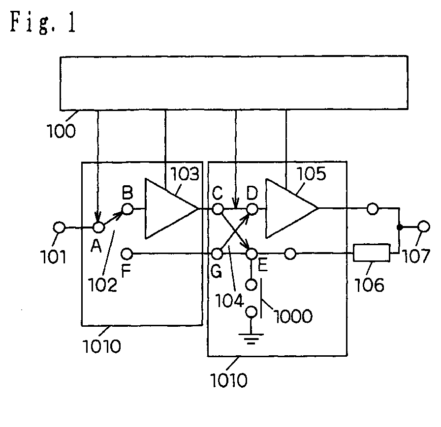
- Fig. 1 is a block diagram of a power amplifier of a first
embodiment of the invention.
- Figs. 2(a) and 2(b) are graphs illustrating the operation
of the power amplifier of the first embodiment.
- Fig. 3 is a block diagram of a power amplifier of a second
embodiment.
- Fig. 4 is a graph illustrating the operation of the power
amplifier of the second embodiment.
- Fig. 5 is a block diagram of a power amplifier of a third
embodiment.
- Fig. 6(a) is a block diagram of a high-frequency switch
section of a power amplifier of a fourth embodiment,
- Fig. 6(b) is a circuit diagram of the high-frequency switch
section of the power amplifier of the fourth embodiment, and
- Fig. 6(c) is a circuit diagram of a further improved
high-frequency switch section.
- Fig. 7(a) is a block diagram of a high-frequency switch
section of a power amplifier of a fifth embodiment, and
- Fig. 7(b) is a circuit diagram of the high-frequency switch
section of the power amplifier of the fifth embodiment.
- Fig. 8 is a block diagram of a power amplifier of a sixth
embodiment.
- Fig. 9 is a view illustrating the operation of the power
amplifier of the sixth embodiment.
- Fig. 10(a) is a block diagram of a high-frequency switch
section of a power amplifier of a seventh embodiment, and
- Fig. 10(b) is a circuit diagram of the high-frequency switch
section of the power amplifier of the seventh embodiment.
- Fig. 11 is a side view of a substrate and its periphery
in an embodiment of the invention.
- Fig. 12 is a diagram showing the configuration of an
embodiment of the communication equipment of the invention.
- Fig. 13 is a diagram showing the configuration of a power
amplifier of the conventional art.
- Fig. 14 is a view illustrating the operation of the power
amplifier of the conventional art.
-
[Description of the Reference Numerals and Signs]
-
- 100, 300, 400, 610
- bias control circuit
- 101, 301, 401, 701, 601
- input terminal
- 102, 302, 402, 602
- first high-frequency switch circuit
- 103, 303, 403, 702
- preamplifier
- 104, 304, 404, 605
- second high-frequency switch circuit
- 105, 307, 405, 703
- postamplifier
- 106, 308, 406
- quarter wavelength line (impedance conversion
circuit)
- 107, 309, 407, 609, 704
- output terminal
- 305
- middle amplifier
- 306
- third high-frequency switch circuit
- 408
- first predistortion circuit
- 409
- second predistortion circuit
- 603
- amplifier
- 606
- first final amplifier
- 607
- second final amplifier
- 608
- transmission line (impedance conversion circuit)
- 1010
- amplification circuit
PREFERRED EMBODIMENTS OF THE INVENTION
-
Hereinafter, embodiments of the power amplifier of the
invention will be described with reference to the accompanying
drawings.
(Embodiment 1)
-
A first embodiment of the invention will be described with
reference to Figs. 1 and 2. Fig. 1 is a block diagram of a power
amplifier of the first embodiment. The reference numeral 100
denotes a bias control circuit, 101 denotes an input terminal,
102 denotes a first high-frequency switch circuit which switches
one input to two outputs, 103 denotes a preamplifier, 104 denotes
a second high-frequency switch circuit which independently
switches two inputs to two outputs, 105 denotes a postamplifier,
106 denotes a quarter wavelength line (impedance conversion
circuit), and 107 denotes an output terminal. The amplification
circuit 1010 according to the invention is a combination of the
high-frequency switch circuits and the amplifiers.
-
In the power amplifier of the embodiment, when the maximum
power must be output, connection between A and B is made in the
first high-frequency switch circuit 102, and connection between
C and D is made in the second switch. At this time, the impedance
of a terminal E of the second switch is short-circuited (or set
to be low), whereby the impedance when seeing the terminal E from
an output terminal of the postamplifier 105 via the quarter
wavelength line 106 is converted into open (high impedance). In
Fig. 1, 1000 denotes a switch for causing the short circuit.
-
According to this configuration, a signal which is input
via the input terminal 101 is amplified by the preamplifier 103,
and then further amplified by the postamplifier 105. An output
signal of the postamplifier is output to the output terminal 107.
-
When the output power is reduced from the maximum point
by a degree corresponding to the gain of the postamplifier,
connection between C and E is made in the second high-frequency
switch circuit 104 while maintaining the connection between A
and B in the first high-frequency switch circuit 102 of Fig. 1.
The bias current of the postamplifier 105 is then interrupted
by the bias control circuit 100.
-
At this time, the bias control circuit performs the bias
control so that the impedance when seeing the output of the
postamplifier 105 from the point where the quarter wavelength
line 106 is connected to the output terminal 107 is set to be
high.
-
Therefore, the signal which is input via the input terminal
101 is amplified by the preamplifier 103, and then bypasses around
the postamplifier 105 to be transmitted to the output terminal
107 via the quarter wavelength line 106.
-
When the output power is further reduced by a degree
corresponding to the gain of the preamplifier, connection between
A and F is made in the first high-frequency switch circuit 102,
and connection between G and E is made in the second high-frequency
switch circuit 102. The bias currents of the preamplifier 103
and the postamplifier 105 are then interrupted by the bias control
circuit 100. Therefore, the signal which is input via the input
terminal 101 bypasses around the preamplifier 103 and the
postamplifier 105 to be transmitted to the output terminal 107.
-
Fig. 2 shows variations of the consumed current with respect
to the output power of the power amplifier. When the power
amplifier operates as described above, the power amplifier has
consumed current characteristics indicated by the thick line in
Fig. 2(a). Namely, the consumed current can be largely reduced
as compared with the case where the amplifiers are not bypassed.
-
In the figure, PMAX indicates the maximum transmission
power, PLEV1 indicates "PMAX - the gain of the postamplifier",
and PLEV2 indicates "PLEV1 - the gain of preamplifier".
-
At each boundary where the bypassing operation on one or
both of the preamplifier and the postamplifier is to be started
or stopped, as shown in Fig. 2(b), the value of the power at which
the transmission power is reduced and the bypassing operation
is started may be shifted from that of the power at which the
transmission power is increased and the bypassing operation is
stopped. In this configuration, the switching frequency of the
bypassing operation can be reduced.
(Embodiment 2)
-
A second embodiment of the invention will be described
with reference to Fig. 3. Fig. 3 is a block diagram of a power
amplifier of the second embodiment. The reference numeral 300
denotes a bias control circuit, 301 denotes an input terminal,
302 denotes a first high-frequency switch circuit which switches
one input to two outputs, 303 denotes a preamplifier, 304 denotes
a second high-frequency switch circuit which independently
switches two inputs to two outputs, 305 denotes a middle amplifier,
306 denotes a third high-frequency switch circuit which
independently switches two inputs to two outputs, 307 denotes
a postamplifier, 308 denotes a quarter wavelength line, and 309
denotes an output terminal.
-
The power amplifier of the second embodiment of the
invention is configured by: the input terminal 301; the first
high-frequency switch circuit 302 which switches a signal input
via the input terminal 301 to two outputs; the first amplifier
(preamplifier) 303 which is connected to one of the outputs of
the first high-frequency switch circuit 302; the second
high-frequency switch circuit 304 which independently switches
two inputs respectively connected to an output of the first
amplifier 303 and the other output of the first high-frequency
switch circuit 302, to two outputs; the second amplifier (middle
amplifier) 305 which is connected to one of the outputs of the
second high-frequency switch circuit 304; the third
high-frequency switch circuit 306 which independently switches
two inputs respectively connected to an output of the second
amplifier 305 and the other output of the second high-frequency
switch circuit 304, to two outputs; the third amplifier
(postamplifier) 307 which is connected to one of the outputs of
the third high-frequency switch circuit 306; the quarter
wavelength line 308 which is connected to the other output of
the third high-frequency switch circuit 306; and the bias control
circuit 300 which controls the power source voltages of the first,
second, and third amplifiers 303, 305, and 307.
-
In the embodiment, the first embodiment is modified so
that the bypass circuit is expanded to an amplifier of a lower
transmission power. When the embodiment is operated in a similar
manner as the first embodiment, the consumed current can be reduced
as shown in Fig. 4.
-
It is apparent that, when the transmission power is further
reduced, the consumed current can be further reduced by disposing
another bypass circuit in a more preceding stage in the same
procedure. In other words, amplification circuits 1010
(combinations of a high-frequency switch circuit and an amplifier)
can be connected at any N stages.
(Embodiment 3)
-
A third embodiment of the invention will be described with
reference to Fig. 5. Fig. 5 is a block diagram of a power amplifier
of the third embodiment. The reference numeral 400 denotes a
bias control circuit, 401 denotes an input terminal, 402 denotes
a first high-frequency switch circuit which switches one input
to two outputs, 403 denotes a preamplifier, 404 denotes a second
high-frequency switch circuit which independently switches two
inputs to two outputs, 405 denotes a postamplifier, 406 denotes
a quarter wavelength line, 407 denotes an output terminal, 408
denotes a first predistortion circuit which previously
compensates distortion generated in the preamplifier, and 409
denotes a second predistortion circuit which previously
compensates distortion generated in the postamplifier.
-
The power amplifier of the third embodiment of the invention
is characterized in that, in addition to the configuration of
the first embodiment, the first predistortion circuit (first
predistortion compensation circuit) 408 is disposed between the
first high-frequency switch circuit 402 and the first amplifier
(preamplifier) 403, and the second predistortion circuit (second
predistortion compensation circuit) 409 is disposed between the
second high-frequency switch circuit 404 and the second amplifier
(postamplifier) 405.
-
The first and second predistortion circuits of Fig. 5
previously correct one or both of amplitude distortion and phase
distortion of the preamplifier and the postamplifier, whereby
nonlinear distortion of the whole of the amplifier can be reduced.
-
At this time, the initial currents of the amplifiers can
be reduced by an amount corresponding to the improved degree of
the distortion. In this case, even in a range where the bypass
circuit is not switched, reduction of the consumed current in
a reduced transmission power can be realized. It is a matter
of course that an unnecessary current can be reduced by the bias
control same as that described in the first embodiment.
-
The predistortion compensation circuits are placed in
front of the first and second amplifiers, respectively. Even
when a predistortion compensation circuit is used only for one
of the amplifiers, it is possible to reduce nonlinear distortion
of the whole of the amplifier.
-
In the above, the example in which predistortion
compensation circuits are used in the configuration of the power
amplifier of the first embodiment has been described. Also when
predistortion compensation circuits are used in the power
amplifier of the second embodiment, nonlinear distortion of the
whole of the amplifier can be similarly reduced.
(Embodiment 4)
-
A fourth embodiment of the invention will be described
with reference to Fig. 6. Fig. 6 is a block diagram of a power
amplifier of the fourth embodiment. Fig. 6 shows the
high-frequency switch circuit of the first embodiment. In the
figure, (a) is a block diagram of the circuit, (b) is a diagram
of the circuit, (c) is a diagram of a circuit which is an improvement
of the circuit of (b), and A to E denote terminals of the
high-frequency switch circuit. In order to simplify the
description, each of transistors Q1 to Q8 in Fig. 6(c), and
transistors Q1 to Q12 in Fig. 6(b) is shown in a state where the
gate terminal is opened. Actually, however, the gate terminal
is connected to the bias control circuit via a serial protection
resistor and a parallel bypass capacitor for reducing noise
components.
-
In the high-frequency switch circuit of (c), the number
of transistors can be decreased by four as compared with the switch
configuration of (b), and therefore the circuit can be miniaturized,
thereby enabling the circuit to be easily integrated into an IC.
-
The high-frequency switch circuit shown in Fig. 6(c)
comprises: the first input terminal A; the first transistor Q2
in which one of the drain and the source is connected in series
to the first input terminal A, the first output terminal B being
connected to the other one of the drain and the source of the
first transistor Q2, one of the drain and the source of the second
transistor Q1 in which the other one of the drain and the source
is grounded in a high-frequency manner being connected to the
first output terminal B; the third transistor Q3 in which one
of the drain and the source is connected in series to the first
input terminal A, the second output terminal E being connected
to the other one of the drain and the source of the third transistor
Q3, one of the drain and the source of the fourth transistor Q4
in which the other one of the drain and the source is grounded
in a high-frequency manner being connected to the second output
terminal E; the fifth transistor Q5 in which one of the drain
and the source is connected in series to the second output terminal
E, the second input terminal C being connected to the other one
of the drain and the source of the fifth transistor Q5, one of
the drain and the source of the sixth transistor Q6 in which the
other one of the drain and the source is grounded in a high-frequency
manner being connected to the second input terminal C; and the
seventh transistor Q7 in which one of the drain and the source
is connected in series to the second input terminal C, the third
output terminal D being connected to the other one of the drain
and the source of the seventh transistor Q7, one of the drain
and the source of the eighth transistor Q8 in which the other
one of the drain and the source is grounded in a high-frequency
manner being connected to the third output terminal D.
-
In the circuit, when voltages applied to the gate terminals
of the transistors are controlled as shown in Table 1 below, the
effects described in the first embodiment are attained.
| state of transmission power | Q1 | Q2 | Q3 | Q4 | Q5 | Q6 | Q7 | Q8 |
| PLEV1 ∼ PMAX | L | H | L | H | L | L | H | L |
| PLEV2 ∼ PLEV1 | L | H | L | L | H | L | L | H |
| PLEV2 or lower | H | L | H | L | L | H | L | H |
PMAX: maximum transmission power
PLEV1: PMAX - gain of postamplifier
PLEV2: PLEV1 - gain of preamplifier
H: potential at which transistor is conductive
L: potential at which transistor is nonconductive |
-
When at least one of the transistors Q1 and Q2 is
appropriately biased so as to perform a predistortion operation,
the effects of the third embodiment can be attained without adding
a special predistortion circuit.
-
Similarly, when at least one of the transistors Q6, Q7,
and Q8 is appropriately biased so as to perform a predistortion
operation, the effects of the third embodiment can be attained
without involving a special predistortion circuit.
(Embodiment 5)
-
A fifth embodiment of the invention will be described with
reference to Fig. 7. Fig. 7 is a block diagram of a power amplifier
of the fifth embodiment. Fig. 7 shows the high-frequency switch
circuit of the second embodiment. In the figure, (a) is a block
diagram of the circuit, (b) is a diagram of the circuit, and A
to K denote terminals of the switch circuit.
-
In order to simplify the description, each of transistors
Q1 to Q14 in Fig. 7(b) is shown in a state where the gate terminal
is opened. Actually, however, the gate terminal is connected
to the bias control circuit via a serial protection resistor and
a parallel bypass capacitor for reducing noise components. In
the same manner as the fourth embodiment, the number of transistors
in the circuit can be decreased by six as compared with the
conventional configuration, and the circuit can be miniaturized,
thereby enabling the circuit to be easily integrated into an IC.
The conventional configuration is for example such circuit that
the circuit part of Q1 to Q11 in Fig. 6(b) is added to the whole
circuit of the Fig. 6(b) while the output terminal E is connected
with the input terminal of said added part circuit. The number
of the transistors in the conventional configuration is 20 but
the Fig. 7(b) is only 14 and the six transistors can be reduced.
-
The high-frequency switch circuit shown in Fig. 7(b)
comprises: the first input terminal A; the first transistor Q2
in which one of the drain and the source is connected in series
to the first input terminal A, the first output terminal B being
connected to the other one of the drain and the source of the
first transistor Q2, one of the drain and the source of the second
transistor Q1 in which the other one of the drain and the source
is grounded in a high-frequency manner being connected to the
first output terminal B; the third transistor Q3 in which one
of the drain and the source is connected in series to the first
input terminal A, one of the drain and the source of the fourth
transistor Q4 in which the other one of the drain and the source
is grounded in a high-frequency manner being connected to the
other one of the drain and the source of the third transistor
Q3; the fifth transistor Q5 in which one of the drain and the
source is connected in series to the other one of the drain and
the source of the third transistor Q3, the second input terminal
C being connected to the other one of the drain and the source
of the fifth transistor Q5, one of the drain and the source of
the sixth transistor Q6 in which the other one of the drain and
the source is grounded in a high-frequency manner being connected
to the second input terminal C; the seventh transistor Q7 in which
one of the drain and the source is connected in series to the
second input terminal C, the second output terminal D being
connected to the other one of the drain and the source of the
seventh transistor Q7, one of the drain and the source of the
eighth transistor Q8 in which the other one of the drain and the
source is grounded in a high-frequency manner being connected
to the second output terminal D; the ninth transistor Q9 in which
one of the drain and the source is connected in series to the
other one of the drain and the source of the third transistor
Q3, the third output terminal K being connected to the other one
of the drain and the source of the ninth transistor Q9, one of
the drain and the source of the tenth transistor Q10 in which
the other one of the drain and the source is grounded in a
high-frequency manner being connected to the third output terminal
K; the eleventh transistor Q11 in which one of the drain and the
source is connected in series to the third output terminal K,
the third input terminal H being connected to the other one of
the drain and the source of the eleventh transistor Q11, one of
the drain and the source of the twelfth transistor Q12 in which
the other one of the drain and the source is grounded in a
high-frequency manner being connected to the third input terminal
H; and the thirteenth transistor Q13 in which one of the drain
and the source is connected in series to the third input terminal
H, the fourth output terminal I being connected to the other one
of the drain and the source of the thirteenth transistor Q13,
one of the drain and the source of the fourteenth transistor Q14
in which the other one of the drain and the source is grounded
in a high-frequency manner being connected to the fourth output
terminal I.
-
In the circuit, when voltages applied to the gate terminals
of the transistors are controlled as shown in Table 2 below, the
effects described in the third embodiment are attained.
-
When at least one of the transistors Q1 and Q2 is
appropriately biased so as to perform a predistortion operation,
the effects of the third embodiment can be attained without
involving a predistortion circuit. Similarly, when at least one
of the transistors Q6, Q7, and Q8 is appropriately biased so as
to perform a predistortion operation, the effects of the third
embodiment can be attained without involving a predistortion
circuit.
-
Similarly, when at least one of the transistors Q12, Q13,
and Q14 is appropriately biased so as to perform a predistortion
operation, the effects of the third embodiment can be attained
without involving a predistortion circuit.
(Embodiment 6)
-
A sixth embodiment of the invention will be described with
reference to Figs. 8 and 9. Fig. 8 is a block diagram of a power
amplifier 600 according to the invention. The reference numeral
601 denotes an input terminal, 602 denotes a first high-frequency
switch which switches one input to two outputs, 603 denotes an
amplifier, 604 denotes impedance switching means, 605 denotes
a second high-frequency switch which switches two inputs to three
outputs, 606 denotes a first final amplifier, 607 denotes a second
final amplifier, 608 denotes a transmission line, 609 denotes
an output terminal, and 610 denotes a bias control circuit.
-
When the maximum power must be output, the power amplifier
of the sixth embodiment causes the first high-frequency switch
601 of Fig. 8 to make connection between A and B, and the second
high-frequency switch 605 to make connection among C, D, and E.
At this time, the impedance of a terminal F of the second
high-frequency switch 605 is short-circuited to be lowered, by
closing a switch 1001, whereby the impedance when seeing the
terminal from outputs of the first and second final amplifiers
606 and 607 via the transmission line 608 is converted into an
open-circuit impedance (high impedance).
-
According to this configuration, a signal which is input
via the input terminal 601 is amplified by the amplifier 603,
and then further amplified by the first and second final amplifiers
606 and 607. Output signals of the final amplifiers are output
to the output terminal 609. At this time, since the first and
second final amplifiers 606 and 607 are connected to each other
in parallel and the circuits have usually the same characteristic
impedance, matching is attained by using the impedance switching
means 604.
-
When the transmission power is made sufficient by the
amplifier 603 and the first final amplifier 606, connection between
C and D is made in the second high-frequency switch 605 while
maintaining the connection between A and B in the first
high-frequency switch 602.
-
At this time, the control circuit 610 performs a control
so that the bias current of the second final amplifier 607 is
interrupted, a bias is given so as to set the impedance when seeing
the output of the second final amplifier 607 from the point where
the first final amplifier 606 is connected to the output terminal
609 to be high, and the impedance switching means 604 is turned
off. Therefore, the signal which is input via the input terminal
601 is amplified by the amplifier 603, the amplified signal is
further amplified by the first final amplifier 606, and an output
signal of the amplifier is output to the output terminal 609.
-
When the transmission power is made sufficient by the
amplifier 603 and the second final amplifier 607, connection
between C and E is made in the second high-frequency switch 605
while maintaining the connection between A and B in the first
high-frequency switch 602.
-
At this time, the control circuit 610 performs a control
so that the bias current of the second final amplifier 607 is
interrupted, a bias is given so as to set the impedance when seeing
the output of the first final amplifier 606 from the point where
the second final amplifier 607 is connected to the output terminal
609 to be high, and the impedance switching means 604 is turned
off. Therefore, the signal which is input via the input terminal
601 is amplified by the amplifier 603, the amplified signal is
further amplified by the second final amplifier 607, and an output
signal of the amplifier is output to the output terminal 609.
-
When the output power is further reduced by a degree
corresponding to the gains of the final amplifiers, connection
between C and F is made in the second high-frequency switch 605
while maintaining the connection between A and B in the first
high-frequency switch 602.
-
At this time, the control circuit 610 performs a control
so that the bias currents of the first and second final amplifiers
606 and 607 are interrupted, a bias is given so as to set the
impedances when seeing the outputs of the first second final
amplifiers 606 and 607 from the point where the transmission line
608 is connected to the output terminal 609 to be high, and the
impedance switching means 604 is turned off. Therefore, the
signal which is input via the input terminal 601 is amplified
by the amplifier 603, and the amplified signal bypasses around
the final amplifiers 606 and 607, and then output to the output
terminal 609 via the transmission line 608.
-
When the output power is further reduced by a degree
corresponding to the gain of the amplifier 603, connection between
A and G is made in the first switch 602, and connection between
H and F is made in the second switch 605. At this time, the control
circuit 610 performs a control so that the bias currents of the
first and second final amplifiers 606 and 607 are interrupted,
a bias is given so as to set the impedances when seeing the outputs
of the first second final amplifiers 606 and 607 from the point
where the transmission line 608 is connected to the output terminal
609 to be high, and the impedance switching means 604 is turned
off. Therefore, the signal which is input via the input terminal
601 bypasses around the amplifier 603 and the final amplifiers,
and then output to the output terminal 609 via the transmission
line 608.
-
Fig. 9 shows variations of the consumed current with respect
to the output power of the power amplifier of the sixth embodiment
in the case where the first and second final amplifiers 606 and
607 have different characteristics.
-
When the power amplifier operates as described above, the
power amplifier has consumed current characteristics indicated
by the thick line in Fig. 9. Namely, the consumed current can
be largely reduced as compared with the case where the amplifiers
are not bypassed.
-
In the case where the first and second final amplifiers
606 and 607 have the same characteristics, the efficiency at an
output power which is lower by 3 dB than the maximum output power
may be made equal to that at the maximum output power.
-
As indicated by the broken lines in Fig. 9, the value of
the transmission power at the timing of the bypass switching in
the case where the transmission power is increasing may be shifted
from that in the case where the transmission power is decreasing,
whereby the switching frequency of the bypass switching operation
can be reduced.
(Embodiment 7)
-
Fig. 10 shows the switches_ in Fig. 8 showing the power
amplifier of the sixth embodiment. In the figure, (a) is a block
diagram of the switches, and (b) is a circuit diagram of the switches.
The symbols of the terminals correspond to those of Fig. 8. In
order to simplify the description, each of transistors Q1 to Q10
in Fig. 10(b) is shown in a state where the gate terminal is opened.
Actually, however, the gate terminal is connected to the control
circuit via a serial protection resistor and a parallel bypass
capacitor for reducing noise components.
-
The high-frequency switch circuit shown in Fig. 10(b)
comprises: the first input terminal A; the first transistor Q2
in which one of the drain and the source is connected in series
to the first input terminal A, the first output terminal B being
connected to the other one of the drain and the source of the
first transistor Q2, one of the drain and the source of the second
transistor Q1 in which the other one of the drain and the source
is grounded in a high-frequency manner being connected to the
first output terminal B; the third transistor Q3 in which one
of the drain and the source is connected in series to the first
input terminal A, the second output terminal F being connected
the other one of the drain and the source of the third transistor
Q3, one of the drain and the source of the fourth transistor Q4
in which the other one of the drain and the source is grounded
in a high-frequency manner being connected to the second output
terminal F; the fifth transistor Q5 in which one of the drain
and the source is connected in series to the second output terminal
F, the second input terminal C being connected to the other one
of the drain and the source of the fifth transistor Q5, one of
the drain and the source of the sixth transistor Q6 in which the
other one of the drain and the source is grounded in a high-frequency
manner being connected to the second input terminal C; and the
seventh transistor Q7 in which one of the drain and the source
is connected in series to the second input terminal C, the third
output terminal D being connected to the other one of the drain
and the source of the seventh transistor Q7, one of the drain
and the source of the eighth transistor Q8 in which the other
one of the drain and the source is grounded in a high-frequency
manner being connected to the third output terminal D, one of
the drain and the source of the ninth transistor Q9 being connected
in series to the other one of the drain and the source of the
fifth transistor Q5, one of the drain and the source of the tenth
transistor Q10 in which the other one of the drain and the source
is grounded in a high-frequency manner being connected to the
other one of the drain and the source of the ninth transistor
Q9, the fourth output terminal E being connected to the other
one of the drain and the source of the ninth transistor Q9.
-
In the circuit, when voltages applied to the gate terminals
of the transistors are controlled as shown in Table 3 below, the
effects described in the sixth embodiment are attained. When
at least one of the transistors Q1 and Q2, and similarly at least
one of the transistors Q6, Q7, and Q8, and at least one of the
transistors Q6, Q9, and Q10 are appropriately biased, the power
amplifier is enabled to perform a predistortion operation without
involving a predistortion circuit.
-
When the power amplifier performs a predistortion
operation, nonlinear distortion of the whole of the amplifier
can be reduced, and the initial current can be reduced by an amount
corresponding to the improved degree of the distortion. In this
case, even when the transmission power is lowered in a range where
the bypass circuit is not switched, reduction of the consumed
current can be realized.
| driving power amplifier | Q1 | Q2 | Q3 | Q4 | Q5 | Q6 | Q7 | Q8 | Q9 | Q10 |
| driver amplifier + final amplifiers 1 and 2 | L | H | L | H | L | L | H | L | H | L |
| driver amplifier + final amplifiers 1 | L | H | L | H | L | L | H | L | H | L |
| driver amplifier + final amplifiers 2 | L | H | L | H | L | L | L | H | L | H |
| driver amplifier only | L | H | L | L | H | L | L | H | L | H |
| all amplifiers are off | H | L | H | L | L | H | L | H | L | H |
H: potential at which transistor is conductive
L: potential at which transistor is nonconductive |
-
It is apparent that the bypass switching control which
is described in the sixth embodiment can attain the same effects
in the seventh embodiment also.
-
It is apparent that, even when a part or all of the
high-frequency switch circuits and the amplifiers are formed on
a same semiconductor substrate, the same effects as those described
above can be attained. When the high-frequency switch circuits
and the amplifiers are configured on different semiconductor
substrates, components which are configured by different
materials (for example, gallium arsenide, silicon, and silicon
germanium), or different processes (an electric field transistor,
a bipolar transistor, and the like) and which have excellent
performances can be shared. Therefore, the production cost can
be lowered, and miniaturization of a terminal device can be
realized as a result of the operation based on a single power
source.
-
In Fig. 11, the above-mentioned high-frequency switch
circuits are configured on a first same semiconductor substrate
80, the amplifiers are configured on a second same semiconductor
substrate 81, and the first and second semiconductor substrates
80 and 81 are mounted on a same dielectric substrate 82.
-
It is apparent that, when the switching control in the
bypass switching boundaries which has been described only in the
first embodiment is performed in accordance with the principle
described in the first embodiment, the same effects are attained
also in the second to seventh embodiments.
-
The communication equipment of the invention is a
communication equipment which is characterized in that the
equipment comprises: a power amplifier 931 according to the
invention which has been described above; an antenna 90; a
reception circuit 91; a signal process circuit 93 which processes
a signal from the reception circuit 91 by using the power amplifier
931; and a transmission circuit 92 which performs a transmission
process on a signal supplied from the signal process circuit 93.
[Effects of the Invention]
-
As described above, in the power amplifier of the invention,
in accordance with reduction of the transmission power, the
amplifier of a higher power is bypassed by the high-frequency
switch, and the power source of the bypassed amplifier is cut
off, whereby the efficiency in transmission at a low power can
be improved. By repeating this operation, the efficiency can
be improved in a broad dynamic range in transmission.
-
Furthermore, the initial current of the amplifier itself
of each stage is reduced so that the amplifier operates in a manner
similar to that of Class B, whereby the efficiency at a low output
power can be improved. In this case, although distortion of a
higher degree appears in the amplifiers, predistortion
compensation is performed by using transistors of the
high-frequency switch in the bypass circuit. Therefore, a power
amplifier can be realized in which the initial current is low
in level and an unnecessary current is interrupted at a low output
power can be realized without increasing the circuit scale.