EP1069712A2 - Broadband optical amplifier - Google Patents
Broadband optical amplifier Download PDFInfo
- Publication number
- EP1069712A2 EP1069712A2 EP00401982A EP00401982A EP1069712A2 EP 1069712 A2 EP1069712 A2 EP 1069712A2 EP 00401982 A EP00401982 A EP 00401982A EP 00401982 A EP00401982 A EP 00401982A EP 1069712 A2 EP1069712 A2 EP 1069712A2
- Authority
- EP
- European Patent Office
- Prior art keywords
- optical
- divider
- dielectric multi
- optical amplifier
- combiner
- Prior art date
- Legal status (The legal status is an assumption and is not a legal conclusion. Google has not performed a legal analysis and makes no representation as to the accuracy of the status listed.)
- Granted
Links
Images


Classifications
-
- H—ELECTRICITY
- H04—ELECTRIC COMMUNICATION TECHNIQUE
- H04B—TRANSMISSION
- H04B10/00—Transmission systems employing electromagnetic waves other than radio-waves, e.g. infrared, visible or ultraviolet light, or employing corpuscular radiation, e.g. quantum communication
- H04B10/29—Repeaters
- H04B10/291—Repeaters in which processing or amplification is carried out without conversion of the main signal from optical form
- H04B10/293—Signal power control
- H04B10/294—Signal power control in a multiwavelength system, e.g. gain equalisation
-
- H—ELECTRICITY
- H04—ELECTRIC COMMUNICATION TECHNIQUE
- H04B—TRANSMISSION
- H04B2210/00—Indexing scheme relating to optical transmission systems
- H04B2210/25—Distortion or dispersion compensation
- H04B2210/258—Distortion or dispersion compensation treating each wavelength or wavelength band separately
Definitions
- the present invention relates to an optical amplifier for use in optical fiber communication systems and optical signal processing systems.
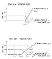
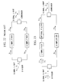
- FIG. 22 The basic configuration of a conventional optical amplifier is shown in Figure 22.
- This optical amplifier is comprised by two amplifying sections having different gain band regions (L-amplifying section and S-amplifying section), a divider, and a combiner, and attempts to broaden the operational bandwidths by coupling the two gain band regions in the wavelength domain.
- L-amplifying section and S-amplifying section two amplifying sections having different gain band regions
- a divider a divider
- a combiner attempts to broaden the operational bandwidths by coupling the two gain band regions in the wavelength domain.
- dividers and combiners are utilized in constructing such optical amplifiers, and they can be classified as a dielectric multi-layer filter or a combination of fiber grating in association with circulator. Those based on dielectric multi-layer filter are reported in the following references.
- wavelength division properties of these devices are not perfect, and problems are encountered depending on the manner and conditions of applying the amplifiers.
- Figures 1A and 1B show the configuration of a conventional optical amplifier, where Figure 1A shows a design based on dielectric multi-layer filters of the long wavelength transmission type (L-type) for the divider and combiner, represented by L-divider (3) and L-combiner (4), and Figure 1B shows a design based on dielectric multi-layer filters of the short wavelength transmission type (S-type) for the divider and combiner, represented by S-divider (5) and S-combiner (6).
- L-type long wavelength transmission type
- S-type short wavelength transmission type
- the amplifying section has a gain medium and a pumping section for excitation, and examples of such optical amplifiers are rare-earth doped fiber amplifier, fiber Raman amplifier and semiconductor laser amplifier.
- the rare-earth doped fiber amplifiers include erbium-doped fiber amplifier and the like, and according to "Wideband erbium-doped fibre amplifiers with three-stage amplification", H. Masuda et. al., IEE Electronics Letters, vol. 34, no. 6, 1998, pp567-568 (Reference 8), it is advantageous when such an amplifier has a gain equalizer to broaden the region of flat gain because such an amplifier can produce a large total gam bandwidth.
- optical amplifiers are generally designed to receive wavelength-multiplexed light signals, and in optical signal processing systems for instruments and the like, optical amplifiers are generally designed to receive wavelength- multiplexed light signals or single wavelength light signals.
- Figures 2A and 2B show configurations of the divider, where Figure 2A represents an L-type dielectric multi-layer filter (L-divider), and Figure 2B represents an S-type dielectric multi-layer filter (S-divider).
- the L-divider receives input light containing a short-wavelength ⁇ s and a long wavelength ⁇ l in the common port (c), and transmits a long wavelength ⁇ l from the transmission port ( l ) and reflects a short wavelength ⁇ s from the reflection port (s).
- the S-divider receives input light containing a short-wavelength ⁇ s and a long wavelength ⁇ l in the common port (c), and reflects a long wavelength light ⁇ l from the reflection port ( l ) and transmits a short wavelength light ⁇ s from the transmission port (s).
- Figures 3A and 3B show configurations of the combiner, where Figure 3A represents an L-type dielectric multi-layer filter (L-combiner), and Figure 3B represents an S-type dielectric multi-layer filter (S-combiner).
- the L-combiner receives input light containing a short-wavelength ⁇ s from the reflection port (s) and a long wavelength ⁇ l from the transmission port ( l ), and outputs light containing a long wavelength ⁇ l and a short wavelength ⁇ s from the common port (c).
- the S-combiner receives input light containing a short-wavelength ⁇ s from the transmission port (s) and a long wavelength ⁇ l from the reflection port ( l ), and outputs light containing a long wavelength ⁇ l and a short wavelength ⁇ s from the common port (c).
- the dividers (L- and S-dividers) 3,.5 perform the steps described above, and divide the multiplexed signal light containing a long wavelength ⁇ l and a short wavelength ⁇ s into a long wavelength signal light ⁇ l and a short wavelength signal light ⁇ s, which are input into the respective amplifying sections (L-a and S-amplifying sections) 1, 2, and are combined in the combiners 4, 6 and multiplexed light signals are thus output.
- Figures 4A and 4B show gain spectra obtained in the amplifying sections (L-, S-amplifying sections) 1, 2, where Figure 4A shows an overall view of the gain region while Figure 4B shows details of gains in the vicinities of the wave boundaries (wavelengths ⁇ tr-s to ⁇ tr- l ) of the L- and S-amplifying sections.
- wavelengths in the L-amplifying section are denoted by ⁇ l * and those in the S-amplifying section are denoted by ⁇ s*
- the peak gains in the L-, S-amplifying sections are denoted by G while the wavelength-specific gains for ⁇ l *, ⁇ s* are denoted by G*.
- Figures 5A and 5B show loss spectra in the L-divider, and show the losses relating to a transmission loss between ports c and s, and the same between ports c and l (refer to Figures 2A and 2B), which are denoted respectively by Lcs1 and Lc l 1 where 1 indicates that the losses are related to long wavelengths.
- Figure 5A shows the loss in the overall view of the gain region and
- Figure 5B shows the details of the loss in the wave boundary.
- the loss becomes larger as the wavelength of the signal waves moves away from the respective boundary wavelengths (wavelengths ⁇ tr-s to ⁇ tr- l ) into fringes of the respective gain regions.
- the loss Lcs1 between the port s (for reflected light) and the common port c is limited to a certain constant value, because of the contribution from residual reflection components in the dielectric multi-layer filter.
- the difference in the wavelengths ⁇ tr-s to ⁇ tr- l (referred to as the boundary bandwidth) is typically 5 ⁇ 10 nm at a 15 ⁇ m wavelength, and the limiting value and the loss at the wavelength ⁇ s* are typically about 10 dB and 20 dB, respectively.
- the boundary bandwidth and the slope of the curve of loss spectrum in the vicinity of the wave boundary are dependent on the parameters (composition and the number of layers of lamination) of the dielectric multi-layer filter.
- Figures 6A and 6B show the loss spectra of the S-type divider, where Figure 6A, 6B relate, respectively, to the transmission losses between ports s and l , and between ports c and l shown in Figures 2A and 2B (referred to as Lcs2, Lc l 2, where 2 indicates that the losses are related to short wavelengths).
- Figure 6A refers to the overall view of the loss region and Figure 6B shows details of losses in the wave boundary.
- Both Lcs2, Lc l 2 show a tendency to increase as the wavelengths of the signal waves move away from the respective boundary wavelengths (wavelengths ⁇ tr-s to ⁇ tr- l ) into fringes of the gain regions.
- the loss Lcs2 between the port l (for reflected light) and the common port c is limited to a certain constant value, which is caused by the contribution from residual reflection components in the dielectric multi-layer filter.
- the difference in the wavelengths ⁇ tr-s to ⁇ tr- l (referred to as the boundary bandwidth) is typically 5 ⁇ 10 nm at a 15 ⁇ m wavelength, and the limiting value and the loss at the wavelength ⁇ s* are typically about 10 dB and 20 dB, respectively.
- the boundary bandwidth and the slope of the curve of loss spectrum in the vicinity of the wave boundary are dependent on the parameters (composition and the number of layers of lamination) of the dielectric multi-layer filter.
- the loss spectra of the L- and S-type combiners are the same as the loss spectra of the L- and S-type dividers shown in Figures 5 and 6, because of the reciprocality of light propagation. That is, if the transmission ports are the same, the loss values are the same.
- Figures 7A and 7B show loss spectra in the optical circuits of a conventional optical amplifier. The losses are incurred in the L- and S-amplifying sections, and the circuit loss is represented by a sum of the losses in the dividers and combiners, and are expressed in the units of dB.
- Figure 7A shows the losses in the L-type divider and combiner shown in Figure 1A
- Figure 7B shows the losses in the S-type divider and combiner shown in Figure 1B.
- the loss value (denoted by L l ) in the S-amplifying section at a wavelength ⁇ l * is limited to 20 dB, which is twice the limit value (about 10 dB).
- 20 dB and 10 dB correspond to non-dimensional numbers, 100 and 10, respectively, so that the former is ten times the latter.
- the loss value (denoted by Ls) in the L-amplifying section at a wavelength ⁇ s* is limited to 20 dB, which is twice the limit value (about 10 dB). In other words, the loss of signal light at the wavelength ⁇ s* is limited to ten times the limit value.
- the output light for example wavelength ⁇ l *, from its primary circuit (through the L-amplifying section) is affected by the contribution from the residual light in the reflection circuit (through the S-amplifying section).
- the optical powers of the primary output light and the residual light are designated, respectively, by P and P*. If the value of P* is not sufficiently small compared with P, coherent interference is generated and interference noise will be superimposed on the signal light to cause operational problems. For example, in an optical communication system, an increase in bit error rate will lead to degradation of the system performance.
- P and P* are related to the input power Pin (in units of dBm) according to the following expressions.
- P-P* G - G* + L l
- G* is the gain in the residual circuit
- L l represents the circuit loss described in Figures 7A and 7B, and wavelength-dependent losses in the dividers and combiners are neglected for simplicity. If it is assumed that the difference between G and G* is smaller than L l and can be neglected, the difference between P and P* is equal to L 1 from equation (2). In the example given in Figures 7A and 7B, L l is about 20 dB, but this value is not sufficiently large, so that interference noise is generated.
- P and P* are related to the input power Pin (in units of dBm) according to the following expressions.
- P-P* G - G* + Ls
- Ls represents the circuit loss described in Figures 7A and 7B. If it is assumed, for simplicity, that the difference between G and G* is smaller than Ls and can be neglected, the difference between P and P* is equal to Ls from equation (4). In the example given in Figures 7A and 7B, Ls is about 20 dB, but this value is not sufficiently large, so that interference noise is generated.
- the signal wavelength in the long wavelength region to produce a gain difference G-G* of less than 10 dB is designated by ⁇ l ** as indicated in Figures 4A and 4B, and the gain value at this wavelength is designated by G**.
- the optical power difference P-P* is less than 30 dB.
- an optical amplifier comprising: an optical divider for dividing input signal light according to wavelengths; two amplifying sections disposed in parallel and having different wavelength amplification regions for amplifying respective light signals emitted from the optical divider; an optical combiner for combining the light signals output from the respective amplifying sections; and an optical filter disposed in series with at least one of the two amplifying sections for generating a loss in a specific wavelength region.
- the optical amplifier of such a design enables to narrow the latent noise region by the action of the filter in generating a loss in residual reflection components created by the wave division effect in the optical divider so as to increase the gain performance of the signal processing circuit associated with the optical filter.
- the object has also been achieved in another design of the optical amplifier comprising: an optical divider using a dielectric multi-layer filter for dividing input signal light according to wavelengths; two amplifying sections disposed in parallel and having different wavelength amplification regions for amplifying respective light signals emitted from the optical divider; and an optical combiner for combining light signals output from respective amplifying sections using a filter having a blocking wavelength region different than the dielectric multi-layer filter provided in the optical divider.
- the optical amplifier of such a design enable to narrow the latent noise region as a result of improved gain in the signal processing circuits because the transmission region of the dielectric multi-layer filter used in the optical divider is different than the dielectric multi-layer filter used in the optical combiner.
- the present optical amplifier provides benefits that the wavelength bandwidth of the latent noise region has been narrowed and, consequently, the bandwidth of useable wavelengths of signal light that can be used for optical processing purposes has been broadened.
- Figures 1A, 1B are schematic diagrams of the configurations of an optical amplifier according to the conventional technology.
- Figures 2A, 2B are schematic diagrams of conventional L-type and S-type dividers.
- Figures 3A, 3B are schematic diagrams of conventional L-type and S-type combiners.
- Figures 4A, 4B are graphs showing the gain spectra in the conventional amplifying section.
- Figures 5A, 5B are graphs showing the loss spectra in a conventional L-type divider (and an L-type combiner).
- Figures 6A, 6B are graphs showing the loss spectra in a conventional S-type divider (and an S-type combiner).
- Figures 7A, 7B are graphs showing the circuit loss spectra in the conventional optical amplifier.
- Figures 8A, 8B are schematic diagrams of the first configuration of the optical amplifier of the present invention.
- Figure 9 is a graph showing the circuit loss spectrum in the first configuration.
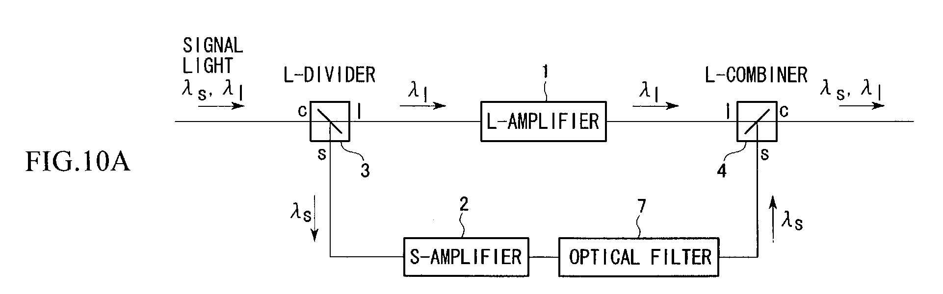
- Figures 10A, 10B are schematic diagrams of the second configuration of the optical amplifier of the present invention.
- Figure 11 is a graph showing a circuit loss spectrum in the second configuration of the optical amplifier of the present invention.
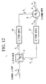
- Figure 12 is a schematic diagram of the configuration of Embodiment 1 of the optical amplifier of the present invention.
- Figure 13A, 13B are graphs showing the gain spectra of the optical amplifier in the first embodiment.
- Figure 14 is a graph showing the circuit loss spectrum in Embodiment 1.
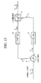
- Figure 15 is a schematic diagram of the configuration of the optical amplifier in Embodiment 2 of the present invention.
- Figures 16A, 16B are graphs showing the gain spectra in the amplifying section in Embodiment 2.
- Figure 17 is a graph showing the circuit loss in Embodiment 2.
- Figure 18 is a schematic diagram of the configuration of the optical amplifier in Embodiment 3.
- Figure 19 is a graph showing the circuit loss spectrum in Embodiment 3.
- Figure 20 a schematic diagram of the configuration of the optical amplifier in Embodiment 4.
- Figure 21 is a graph showing the circuit loss spectrum in Embodiment 4.
- Figure 22 is a schematic diagram of the basic configuration of the conventional optical amplifier.
- Figure 23 is a schematic diagram of the third configuration of the optical amplifier of the present invention.
- Figure 24 is a schematic diagram of the configuration of the optical amplifier in Embodiment 5 of the present invention.
- Figure 25 is a schematic diagram of the configuration of the optical amplifier in Embodiment 6 of the present invention.
- Figure 8A shows a configuration based on an L-type divider and an S-type combiner (referred to as L-divider and S-combiner hereinafter), and Figure 8B shows a configuration based on an S-divider and an L-combiner.
- Figure 9 shows the circuit loss spectra of the amplifier in the first configuration, relating the circuit losses through the L- and S-amplifying sections, representing a sum of the losses in the divider and combiner in units of decibels (dB).
- This loss spectra are obtained from the loss spectra shown in Figures 5 and 6 which were explained in the section on the related art.
- the loss values are typical values as described in the section concerned with the related art.
- the wavelength region that shows less than 30 dB power difference, P-P*, in Figure 9 occurs from the vicinity of ⁇ s* to the vicinity of ⁇ l *.
- This difference in the wavelengths (difference between the wavelengths in the vicinities of ⁇ s* and ⁇ l *) is considerably smaller than the difference in the corresponding wavelengths (difference between the wavelengths in the vicinities of ⁇ s** and ⁇ l **) described in the section concerned with the related art. That is, according to the first configuration, bandwidth of the signal waves affected by the interference noise is narrower compared with that of conventional amplifiers, because the residual reflection components have been reduced, thus enabling to expand the useable bandwidth of signal waves.
- Figure 10A shows a configuration based on an L-divider and an L-combiner
- Figure 10B shows a configuration based on an S-divider and an S-combiner.
- the optical filter 7 in Figure 10A is a short wavelength transmission type and the optical filter 8 in Figure 10B is a long wavelength transmission type.
- the filters 7, 8 include 2-port optical filters having dielectric multi-layer filters or fiber gratings that reflect those signal waves having wavelengths in the vicinities of boundary wavelengths.
- optical amplifiers based on such filters 7 and 8 utilizing 2-port optical filter are made of dielectric multi-layer filters, amplifiers can be produced at lower cost compared with amplifiers based on other types of optical filters, because of the low cost of making dielectric multi-layer filters.
- the filters 7 and 8 are made of fiber gratings, optical amplifiers utilizing such filters are advantageous because the insertion losses due to insertion of signal waves are smaller compared with the insertion losses experienced by other types of filters so that higher gain and output power as well as lower interference noise can be obtained from such optical amplifiers.
- optical filters 7, 8 are placed in the aft-stage of the L- and S-amplifying sections, they may be placed in series in the fore-stage.
- the aft-stage placement is more advantageous than the fore-stage placement, because the interference noise is lower in such an arrangement.
- Figure 11 shows a circuit loss spectrum of the optical amplifier based on the second configuration, especially the use of an L-divider and an L-combiner, shown in Figure 10A.
- the optical filter 7 in this case is based on a 2-port optical filter having dielectric multi-layer filters, relating the circuit losses through the L- and S-amplifying sections, and representing a sum of the losses in the divider and combiner in units of decibels (dB).
- dB decibels
- the wavelength region that shows less than 30 dB power difference, P-P*, in Figure 11 occurs from the vicinity of ⁇ s** to the vicinity of ⁇ tr- l .
- This difference in the wavelengths (difference between the wavelengths in the vicinities of ⁇ s** and ⁇ tr- l ) is considerably small than the difference in the corresponding wavelengths described in the section concerned with the related art. That is, according to the second configuration, bandwidth of the signal waves affected by the interference noise is narrower compared with that of conventional amplifiers, thus enabling to expand the bandwidth of useable signal wavelengths.
- Figure 23 shows a third configuration of the optical amplifier.
- the divider (1:1 division) and combiner are either fiber couplers (combiners), whose performance properties do not vary with wavelengths, or a combination of a fiber coupler and either a divider or a combiner made of dielectric multi-layer filters.
- the signal wavelength ⁇ s in the short wavelength band is close to the wavelengths in the wave boundary between the long and short wavelength bands, such signal waves tend to mix with the long wavelengths in the long wavelength L-amplifying section, and therefore, such mixed wave components are eliminated by placing an optical filter in the aft-stage of the L-amplifying section.
- the loss value in the optical filter for the mixed waves should be higher than 30 dB for the same reasons as explained earlier.
- the fiber grating clearly serves a different purpose than the optical filter provided in the present invention as a constituting element for the purpose of eliminating residual reflection components.
- Figure 12 shows an optical amplifier in Embodiment 1. This is an example of using an erbium doped fiber amplifier (EDFA) in the amplifying section.
- EDFA erbium doped fiber amplifier
- a regular EDFA for short wavelength band (S-type EDFA) 11 is used for processing short wavelength signals
- a long wavelength band (L-type EDFA) 12 having the bandwidth enlarged by a gain equalizer, described in the section concerned with the related art, was used for processing long wavelength signals.
- Figures 13A and 13B show schematic diagrams of the gain spectra of the amplifying sections (S-type EDFA and L-type EDFA) in Embodiment 1, where Figure 13A relates to the overall view of the spectrum and Figure 13B relates to the details of the spectrum near the wave boundary.
- the wave boundary extends from 1562 to 1566 nm.
- the number of layers of the dielectric multi-layer filter is approximately 100.
- the peak gain of the amplifying section is 20 dB, and the gains for S-type EDFA and L-type EDFA at 1570 nm are 10 dB for each.
- Figure 14 shows the circuit loss spectrum of the amplifier in Embodiment 1.
- the boundary bandwidth in which the differential power P-P* of the signal waves is less than 30 dB is approximately 1560 ⁇ 1568 nm according to the results shown in Figures 13, 14. It means that the bandwidth of the "latent noise region" is 8 nm. On the other hand, in the conventional optical amplifiers based on L-type divider and S-type combiner, the corresponding boundary bandwidth is approximately 1561 ⁇ 1574, resulting in the bandwidth of the latent noise region of 13 nm.
- the bandwidth of the latent noise region (wavelength region that cannot be used for signal waves because of interference noise effects) in the present optical amplifier is about a half of the conventional width (8/13 to be exact).
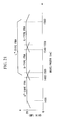
- Figure 15 shows a configuration of the optical amplifier in Embodiment 2.
- SLA semiconductor laser amplifier
- the wavelength gain region of SLA can be changed by varying the semiconductor composition ratio.
- short wavelength band SLA (S-type SLA) 13 and long wavelength band SLA (L-type SLA) 14 are being used, and they have primarily different composition ratios of semiconductors.
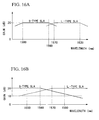
- Figures 16A and 16B show schematic diagrams of the gain spectra of the amplifying sections (S-type and L-type SLA) in this embodiment, where Figure 16A relates to the overall spectrum and Figure 16B relates to the spectrum near the wave boundary.
- the wave boundary extends from 1560 to 1570 nm.
- the number of layers of the dielectric multi-layer filter is approximately 50.
- the peak gain of the amplifying section is 20 dB, and the gains for S-type SLA 13 and L-type SLA 14 at 1585 nm are 10 dB for each.
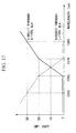
- Figure 17 shows the circuit loss spectrum of the amplifier in this embodiment.
- the boundary bandwidth in which the differential power P-P* of the signal waves is less than 30 dB is approximately 1554 ⁇ 1576 nm according to the results shown in Figures 16, 17. It means that the width of the latent noise region is 22 nm. On the other hand, in the conventional optical amplifiers based on L-divider and S-combiner, the corresponding boundary bandwidth is approximately 1557 ⁇ 1595, resulting in the width of the latent noise region of 38 nm.
- the width of the latent noise region (wavelength region that cannot be used for signal waves because of interference noise effects) in the present optical amplifier is about a half of the conventional width (22/38 to be exact).
- Figure 18 shows a configuration of the optical amplifier in Embodiment 3.
- SLA semiconductor laser amplifier
- the wavelength gain region of SLA can be changed by varying the semiconductor composition ratio.
- short wavelength band SLA (S-type SLA) 13 and long wavelength band SLA (L-type SLA) 14 are being used, they are primarily different in the semiconductor composition ratios.
- the structure of the amplifying section in this embodiment is the same as that in Figures 16A and 16B.
- the number of layers in the dielectric multi-layer filter, L-divider, L-combiner and the optical filter 15 used in the amplifier shown in Figure 18 is approximately 50.
- Figure 19 shows circuit loss spectrum for the amplifier in this embodiment.
- the boundary bandwidth in which the differential power P-P* of the signal waves is less than 30 dB is approximately 1556 ⁇ 1570 nm according to the results shown in Figures 16, 19. It means that the bandwidth of the latent noise region is 14 nm. On the other hand, in the conventional optical amplifiers based on L-divider and L-combiner, the corresponding boundary bandwidth is approximately 1557 ⁇ 1595, giving the width of the latent noise region as 38 nm.
- the width of the latent noise region (wavelength region that cannot be used for signal waves because of interference noise effects) in the present optical amplifier is about a third of the conventional width (14/38 to be exact).
- Figure 20 shows a configuration of the optical amplifier in Embodiment 4. This is an example of using a fiber Raman amplifier (FRA) in the amplifying section.
- FRA fiber Raman amplifier
- the wavelength gain region of FRA can be changed by varying the pumping wavelength.
- the amplifier in this embodiment is a 3-wavelength band amplifier, based on the concept outlined earlier to regard an amplifier for two wavelength bands as one amplifying section.
- a short wavelength band FRA (S-type FRA) 16 and a long wavelength band FRA (L-type FRA) 17 are used to construct a 2-wavelength band optical amplifier, which is designated as the new long wavelength band FRA (L*-type FRA), and a short wavelength band FRA (S*-type FRA) 18 is used at the short wavelength end of the new L*-type FRA, as a third amplifying section, in association with an L-divider (3') and an S-combiner (6').
- the outlines of the gain spectra of the amplifying sections are shown in Figure 21.
- the number of layers of the dielectric multi-layer filters used in the L-divider and S-combiner used in this embodiment is approximately 50. Similar to Embodiment 3, the width of the latent noise region relates, in this case, to the widths of the two wave boundaries in the 3-wavelength bands, and both are 14 nm. On the other hand, in the conventional optical amplifier, the corresponding boundary bandwidth is 38 nm.
- the width of the latent noise region (wavelength region that cannot be used for signal waves because of interference noise effects) in the present optical amplifier is about a third of the conventional width (14/38 to be exact).
- Figure 24 shows a configuration of the optical amplifier in Embodiment 5.
- the amplifying section is comprised by an S-type EDFA for short wavelengths, an L-type EDFA for long wavelengths, and the divider and combiner are made of fiber couplers that are not dependent on wavelength and having a 1:1 split ratio.
- a fiber grating is placed in each aft-stages of the S-EDFA and L-EDFA for eliminating long wavelength signal waves and short wavelength signal waves, respectively, to serve as optical filters, and are respectively referred to as L-fiber-grating and S-fiber-grating.
- the S- and L-EDFA respectively amplify signal waves having wavelengths in a range of 1530 ⁇ 1560 nm and wavelengths in a range of 1570 ⁇ 1600 nm.
- the S-fiber-grating filters only those signal waves having wavelengths in a range of 1550 ⁇ 1560 nm to generate a loss value of more than 20 dB.
- the L-EDFA generates a gain of more than 20 dB for wavelengths of signal waves in a range of 1570 ⁇ 1600 nm, at the same time, a gain of less than 10 dB for wavelengths of signal waves in a range of 1550 ⁇ 1560 nm, and a loss of more than 10 dB for wavelengths of signal waves in a range of 1530 ⁇ 1550 nm.
- the L-fiber-grating filters only those waves having wavelengths in a range of 1570 ⁇ 1600 nm to generate a loss value of more than 20 dB.
- the S-EDFA generates a gain of more than 20 dB for wavelengths of signal waves in a range of 1530 ⁇ 1560 nm, at the same time, a gain of less than 10 dB for wavelengths of signal waves in a range of 1570 ⁇ 1600 nm.
- Fiber gratings having such optical properties can be produced readily at low cost.
- non-useable wavelength range for signal waves is 10 nm that exists between 1560 ⁇ 1570 nm. This value is less than half the value generally observed in the conventional technologies and is clearly less than the conventional amplifiers that do not use L- and S-fiber-gratings.
- the divider and combiner used in the input section and output section of the amplifier have a split ratio of 1: 1 and no wavelength dependency, compared with an amplifier based on wave-separation type divider and combiner such as dielectric multi-layer filters, an excess loss value of nearly 3 dB is generated.
- fiber couplers having a 1:1 split ratio and no wavelength dependency have an advantage that they generally cost less than other types of filters. Also, the excess loss can be compensated by providing additional means.
- Figure 25 shows a configuration of the optical amplifier in Embodiment 6.
- This configuration may appear similar to the one for Embodiment 1, but a significant difference is that the divider is based on a dielectric multi-layer filter and the combiner is based on a fiber coupler having a 1:1 split ratio and no wavelength dependency. Also, an S-fiber-grating is placed in the aft-stage of the L-EDFA as an optical filter for filtering signal waves in the short wavelength band.
- the S-fiber-grating filters only those signal waves having wavelengths in a range of 1550 ⁇ 1560 nm to generate a loss value of more than 10 dB.
- the L-EDFA generates a gain of 20 dB for wavelengths of signal waves in a range of 1570 ⁇ 1600 nm, at the same time, a gain of less than 10 dB for wavelengths of signal waves in a range of 1550 ⁇ 1560 nm, and a loss of more than 10 dB for wavelengths of signal waves in a range of 1530 ⁇ 1550 nm.
- the S-divider generates a loss of more than 10 dB for signal waves in a range of 1530 ⁇ 1560 nm between input port (c) and port ( l ) connecting to the L-EDFA.
- the latent noise bandwidth is 10 nm that exists between 1560 ⁇ 1570 nm. This value is clearly less than the conventional amplifiers that do not use S-fiber-gratings, and is less than half the value generally observed in the conventional technologies.
- the present invention has been demonstrated using examples as described above, but the configurations of the amplifiers are not limited to those demonstrated in specific examples, and includes those circuit designs within the concept outlined in the present invention.
Abstract
- an optical divider for dividing input signal light according to wavelengths,
- two amplifying sections (1, 2) disposed in parallel and having different wavelength amplification regions for amplifying respective light signals emitted from the optical divider,
- an optical combiner for combining the light signals output from the respective amplifying sections, and
- an optical filter disposed in series with at least one of the two amplifying sections for generating a loss in a specific wavelength region.
Description
- The present invention relates to an optical amplifier for use in optical fiber communication systems and optical signal processing systems.
- This application is based on patent application No. Hei 11-197126, the content of which is incorporated herein by reference.
- The basic configuration of a conventional optical amplifier is shown in Figure 22. This optical amplifier is comprised by two amplifying sections having different gain band regions (L-amplifying section and S-amplifying section), a divider, and a combiner, and attempts to broaden the operational bandwidths by coupling the two gain band regions in the wavelength domain. (refer to "Broadband and gain-flattened amplifier composed of a 1.55 µm-band and a 1.58 µm-band Er3+-doped fiber amplifier in a parallel configuration", M. Yamada et. al., IEE Electronics Letters, Vol. 33, No. 8, 1977, pp710-711) (Reference 1).
- Various types of dividers and combiners are utilized in constructing such optical amplifiers, and they can be classified as a dielectric multi-layer filter or a combination of fiber grating in association with circulator. Those based on dielectric multi-layer filter are reported in the following references.
- "Broadband and gain-flattened amplifier composed of a 1.55 µm-band and a 1.58 µm-band Er3+-doped fiber amplifier in a parallel configuration", M. Yamada et. al., IEE Electronics Letters, vol. 33, no. 8, 1977, pp710-711. (Reference 1)
- Japanese Unexamined Patent Application, First Publication, No. Hei 10-229238, Publication Date, August 25, 1998. (Reference 2)
- Japanese Unexamined Patent Application, First Publication, No. Hei 11-204859, Publication Date, July 30, 1999. (Reference 3)
- International Application Published under the Patent Cooperation Treaty, PCT/US98/16558, "Optical amplifier apparatus", International publication date, April 8, 1999, International Publication Number WO 99/17410. (Reference 4)
- Those based on a combination of circulator and fiber grating are reported in the following references.
- European Patent Application,
EP 0 883 218 A1, "Wide band optical amplifier", Publication date 09.12.1998. (Reference 5) - "A gain-flattened ultra wide band EDFA for high capacity WDM optical communication systems", Y.Sun et. al., Technical Digest of ECOC'98, pp.53-54, 1998. (Reference 6)
- The following reference does not specify what type of device is used.
- Japanese Unexamined Patent Application, First Publication, No. Hei 4-101124, Publication Date, April 2, 1992. (Reference 7)
- All of the above references assume that the wavelength division properties are either perfect or present no particular problems.
- However, as will be shown with specific examples in the following, wavelength division properties of these devices are not perfect, and problems are encountered depending on the manner and conditions of applying the amplifiers.
- First, the most common problem of such amplifiers is encountered when the dividers and combiners are made of dielectric multi-layer filters. Figures 1A and 1B show the configuration of a conventional optical amplifier, where Figure 1A shows a design based on dielectric multi-layer filters of the long wavelength transmission type (L-type) for the divider and combiner, represented by L-divider (3) and L-combiner (4), and Figure 1B shows a design based on dielectric multi-layer filters of the short wavelength transmission type (S-type) for the divider and combiner, represented by S-divider (5) and S-combiner (6).
- The amplifying section has a gain medium and a pumping section for excitation, and examples of such optical amplifiers are rare-earth doped fiber amplifier, fiber Raman amplifier and semiconductor laser amplifier. The rare-earth doped fiber amplifiers include erbium-doped fiber amplifier and the like, and according to "Wideband erbium-doped fibre amplifiers with three-stage amplification", H. Masuda et. al., IEE Electronics Letters, vol. 34, no. 6, 1998, pp567-568 (Reference 8), it is advantageous when such an amplifier has a gain equalizer to broaden the region of flat gain because such an amplifier can produce a large total gam bandwidth.
- In optical communication systems, optical amplifiers are generally designed to receive wavelength-multiplexed light signals, and in optical signal processing systems for instruments and the like, optical amplifiers are generally designed to receive wavelength- multiplexed light signals or single wavelength light signals.
- Figures 2A and 2B show configurations of the divider, where Figure 2A represents an L-type dielectric multi-layer filter (L-divider), and Figure 2B represents an S-type dielectric multi-layer filter (S-divider). The L-divider receives input light containing a short-wavelength λs and a long wavelength λl in the common port (c), and transmits a long wavelength λl from the transmission port (l) and reflects a short wavelength λs from the reflection port (s). On the other hand, the S-divider receives input light containing a short-wavelength λs and a long wavelength λl in the common port (c), and reflects a long wavelength light λl from the reflection port (l) and transmits a short wavelength light λs from the transmission port (s).
- Figures 3A and 3B show configurations of the combiner, where Figure 3A represents an L-type dielectric multi-layer filter (L-combiner), and Figure 3B represents an S-type dielectric multi-layer filter (S-combiner). The L-combiner receives input light containing a short-wavelength λs from the reflection port (s) and a long wavelength λl from the transmission port (l), and outputs light containing a long wavelength λl and a short wavelength λs from the common port (c). On the other hand, the S-combiner receives input light containing a short-wavelength λs from the transmission port (s) and a long wavelength λl from the reflection port (l), and outputs light containing a long wavelength λl and a short wavelength λs from the common port (c).
- Referring to Figures 1A and 1B, the dividers (L- and S-dividers) 3,.5, perform the steps described above, and divide the multiplexed signal light containing a long wavelength λl and a short wavelength λs into a long wavelength signal light λl and a short wavelength signal light λs, which are input into the respective amplifying sections (L-a and S-amplifying sections) 1, 2, and are combined in the
combiners - However, there are problems in the performance of the light amplifiers described above, which will be explained in the following.
- Figures 4A and 4B show gain spectra obtained in the amplifying sections (L-, S-amplifying sections) 1, 2, where Figure 4A shows an overall view of the gain region while Figure 4B shows details of gains in the vicinities of the wave boundaries (wavelengths λtr-s to λtr-l) of the L- and S-amplifying sections. In Figure 4B, wavelengths in the L-amplifying section are denoted by λl* and those in the S-amplifying section are denoted by λs*, and the peak gains in the L-, S-amplifying sections are denoted by G while the wavelength-specific gains for λl*, λs* are denoted by G*.
- Figures 5A and 5B show loss spectra in the L-divider, and show the losses relating to a transmission loss between ports c and s, and the same between ports c and l (refer to Figures 2A and 2B), which are denoted respectively by Lcs1 and Lcl1 where 1 indicates that the losses are related to long wavelengths. Figure 5A shows the loss in the overall view of the gain region and Figure 5B shows the details of the loss in the wave boundary. For both Lcs1 and Lcl1, the loss becomes larger as the wavelength of the signal waves moves away from the respective boundary wavelengths (wavelengths λtr-s to λtr-l) into fringes of the respective gain regions.
- However, in the long wavelength side of the loss spectrum (i.e., at the λtr-l end), the loss Lcs1 between the port s (for reflected light) and the common port c is limited to a certain constant value, because of the contribution from residual reflection components in the dielectric multi-layer filter.
- The difference in the wavelengths λtr-s to λtr-l (referred to as the boundary bandwidth) is typically 5∼10 nm at a 15 µm wavelength, and the limiting value and the loss at the wavelength λs* are typically about 10 dB and 20 dB, respectively. The boundary bandwidth and the slope of the curve of loss spectrum in the vicinity of the wave boundary are dependent on the parameters (composition and the number of layers of lamination) of the dielectric multi-layer filter.
- Figures 6A and 6B show the loss spectra of the S-type divider, where Figure 6A, 6B relate, respectively, to the transmission losses between ports s and l, and between ports c and l shown in Figures 2A and 2B (referred to as Lcs2, Lcl2, where 2 indicates that the losses are related to short wavelengths). Figure 6A refers to the overall view of the loss region and Figure 6B shows details of losses in the wave boundary. Both Lcs2, Lcl2 show a tendency to increase as the wavelengths of the signal waves move away from the respective boundary wavelengths (wavelengths λtr-s to λtr-l) into fringes of the gain regions.
- However, in the short wavelength side of the loss spectrum (i.e., at the Xtr-s end), the loss Lcs2 between the port l (for reflected light) and the common port c is limited to a certain constant value, which is caused by the contribution from residual reflection components in the dielectric multi-layer filter.
- The difference in the wavelengths λtr-s to λtr-l (referred to as the boundary bandwidth) is typically 5∼10 nm at a 15 µm wavelength, and the limiting value and the loss at the wavelength λs* are typically about 10 dB and 20 dB, respectively. The boundary bandwidth and the slope of the curve of loss spectrum in the vicinity of the wave boundary are dependent on the parameters (composition and the number of layers of lamination) of the dielectric multi-layer filter.
- The loss spectra of the L- and S-type combiners are the same as the loss spectra of the L- and S-type dividers shown in Figures 5 and 6, because of the reciprocality of light propagation. That is, if the transmission ports are the same, the loss values are the same.
- Figures 7A and 7B show loss spectra in the optical circuits of a conventional optical amplifier. The losses are incurred in the L- and S-amplifying sections, and the circuit loss is represented by a sum of the losses in the dividers and combiners, and are expressed in the units of dB. Figure 7A shows the losses in the L-type divider and combiner shown in Figure 1A, and Figure 7B shows the losses in the S-type divider and combiner shown in Figure 1B.
- In the case of the L-type amplifier, the loss value (denoted by Ll) in the S-amplifying section at a wavelength λl* is limited to 20 dB, which is twice the limit value (about 10 dB). These values, 20 dB and 10 dB, correspond to non-dimensional numbers, 100 and 10, respectively, so that the former is ten times the latter. On the other hand, the case of the S-type amplifier, the loss value (denoted by Ls) in the L-amplifying section at a wavelength λs* is limited to 20 dB, which is twice the limit value (about 10 dB). In other words, the loss of signal light at the wavelength λs* is limited to ten times the limit value.
- As explained above, in the vicinity of the wave boundaries, because the wave separation properties in the dividers and combiners are not perfect, the output light, for example wavelength λl*, from its primary circuit (through the L-amplifying section) is affected by the contribution from the residual light in the reflection circuit (through the S-amplifying section).
- For the purpose of providing a quantitative explanation, the optical powers of the primary output light and the residual light are designated, respectively, by P and P*. If the value of P* is not sufficiently small compared with P, coherent interference is generated and interference noise will be superimposed on the signal light to cause operational problems. For example, in an optical communication system, an increase in bit error rate will lead to degradation of the system performance.
- In the L-type divider and combiner (refer to Figure 1A), P and P* are related to the input power Pin (in units of dBm) according to the following expressions.
- Similarly, in the configuration based on S-type dividers and combiners (refer to Figure 1B), P and P* are related to the input power Pin (in units of dBm) according to the following expressions.
- If it is assumed that 30 dB is a sufficiently high value of the difference P-P* to prevent the interference noise from being generated, in the wavelength regions where the gain difference, G-G*, is less than 10 dB, it is obvious that interference noise cannot be neglected.
- In the amplifier based on L-type dividers and combiners, the signal wavelength in the long wavelength region to produce a gain difference G-G* of less than 10 dB is designated by λl** as indicated in Figures 4A and 4B, and the gain value at this wavelength is designated by G**. Then, as shown in Figure 7A, in the region from the vicinity of the signal wavelength λs** (where the power difference P-P* in the short wavelength region becomes less than 30 dB) to the vicinity the signal wavelength λl**, the optical power difference P-P* is less than 30 dB. Therefore, because of such double adverse effects, i.e., insufficient differences in gain as well as output power levels caused by residual reflection components in both L- and S-devices, interference noise generated in the boundary bandwidth causes degradation in the amplifier performance. Similar results occur in the amplifier based on S-type dividers and combiners, and therefore, it creates a difficulty that the useable wavelengths are restricted in the conventional design of amplifiers regardless of the wavelengths of dividers and combiners.
- As discussed above, in the conventional technologies based on dielectric multi-layer filters, interference noises are unavoidable in the signal waves in the vicinity of the wave boundaries, and therefore, it creates a problem that the useable wavelengths are restricted. Even in those systems using dividers and combiners not based on dielectric multi-layer filters, the same problems are experienced because the wavelength division properties of the dividers and combiners are not perfect.
- It is an object of the present invention to resolve the problems outlined above, and provide an optical amplifier having a broad bandwidth of useable wavelength for processing input signal light.
- According to the present invention, the object has been achieved in an optical amplifier comprising: an optical divider for dividing input signal light according to wavelengths; two amplifying sections disposed in parallel and having different wavelength amplification regions for amplifying respective light signals emitted from the optical divider; an optical combiner for combining the light signals output from the respective amplifying sections; and an optical filter disposed in series with at least one of the two amplifying sections for generating a loss in a specific wavelength region.
- The optical amplifier of such a design enables to narrow the latent noise region by the action of the filter in generating a loss in residual reflection components created by the wave division effect in the optical divider so as to increase the gain performance of the signal processing circuit associated with the optical filter.
- Also, the object has also been achieved in another design of the optical amplifier comprising: an optical divider using a dielectric multi-layer filter for dividing input signal light according to wavelengths; two amplifying sections disposed in parallel and having different wavelength amplification regions for amplifying respective light signals emitted from the optical divider; and an optical combiner for combining light signals output from respective amplifying sections using a filter having a blocking wavelength region different than the dielectric multi-layer filter provided in the optical divider.
- The optical amplifier of such a design enable to narrow the latent noise region as a result of improved gain in the signal processing circuits because the transmission region of the dielectric multi-layer filter used in the optical divider is different than the dielectric multi-layer filter used in the optical combiner.
- Accordingly, the present optical amplifier provides benefits that the wavelength bandwidth of the latent noise region has been narrowed and, consequently, the bandwidth of useable wavelengths of signal light that can be used for optical processing purposes has been broadened.
- The reference numerals appended in the claims do not limit the interpretation of the claims.
- Figures 1A, 1B are schematic diagrams of the configurations of an optical amplifier according to the conventional technology.
- Figures 2A, 2B are schematic diagrams of conventional L-type and S-type dividers.
- Figures 3A, 3B are schematic diagrams of conventional L-type and S-type combiners.
- Figures 4A, 4B are graphs showing the gain spectra in the conventional amplifying section.
- Figures 5A, 5B are graphs showing the loss spectra in a conventional L-type divider (and an L-type combiner).
- Figures 6A, 6B are graphs showing the loss spectra in a conventional S-type divider (and an S-type combiner).
- Figures 7A, 7B are graphs showing the circuit loss spectra in the conventional optical amplifier.
- Figures 8A, 8B are schematic diagrams of the first configuration of the optical amplifier of the present invention.
- Figure 9 is a graph showing the circuit loss spectrum in the first configuration.
- Figures 10A, 10B are schematic diagrams of the second configuration of the optical amplifier of the present invention.
- Figure 11 is a graph showing a circuit loss spectrum in the second configuration of the optical amplifier of the present invention.
- Figure 12 is a schematic diagram of the configuration of
Embodiment 1 of the optical amplifier of the present invention. - Figure 13A, 13B are graphs showing the gain spectra of the optical amplifier in the first embodiment.
- Figure 14 is a graph showing the circuit loss spectrum in
Embodiment 1. - Figure 15 is a schematic diagram of the configuration of the optical amplifier in
Embodiment 2 of the present invention. - Figures 16A, 16B are graphs showing the gain spectra in the amplifying section in
Embodiment 2. - Figure 17 is a graph showing the circuit loss in
Embodiment 2. - Figure 18 is a schematic diagram of the configuration of the optical amplifier in
Embodiment 3. - Figure 19 is a graph showing the circuit loss spectrum in
Embodiment 3. - Figure 20 a schematic diagram of the configuration of the optical amplifier in
Embodiment 4. - Figure 21 is a graph showing the circuit loss spectrum in
Embodiment 4. - Figure 22 is a schematic diagram of the basic configuration of the conventional optical amplifier.
- Figure 23 is a schematic diagram of the third configuration of the optical amplifier of the present invention.
- Figure 24 is a schematic diagram of the configuration of the optical amplifier in
Embodiment 5 of the present invention. - Figure 25 is a schematic diagram of the configuration of the optical amplifier in
Embodiment 6 of the present invention. - The following embodiments do not restrict the interpretation of the claims relating to the present invention, and the combination of all the features explained in the embodiments are not always indispensable means of solving the problem.
- The first configuration of the present optical amplifier is shown in Figures 8A and 8B. Figure 8A shows a configuration based on an L-type divider and an S-type combiner (referred to as L-divider and S-combiner hereinafter), and Figure 8B shows a configuration based on an S-divider and an L-combiner. Figure 9 shows the circuit loss spectra of the amplifier in the first configuration, relating the circuit losses through the L- and S-amplifying sections, representing a sum of the losses in the divider and combiner in units of decibels (dB). This loss spectra are obtained from the loss spectra shown in Figures 5 and 6 which were explained in the section on the related art. The loss values are typical values as described in the section concerned with the related art.
- The wavelength region that shows less than 30 dB power difference, P-P*, in Figure 9 occurs from the vicinity of λs* to the vicinity of λl*. This difference in the wavelengths (difference between the wavelengths in the vicinities of λs* and λl*) is considerably smaller than the difference in the corresponding wavelengths (difference between the wavelengths in the vicinities of λs** and λl**) described in the section concerned with the related art. That is, according to the first configuration, bandwidth of the signal waves affected by the interference noise is narrower compared with that of conventional amplifiers, because the residual reflection components have been reduced, thus enabling to expand the useable bandwidth of signal waves.
- The second configuration of the optical amplifier is shown in Figures 10A and 10B. Figure 10A shows a configuration based on an L-divider and an L-combiner, and Figure 10B shows a configuration based on an S-divider and an S-combiner.
- According to the second configuration, an extra optical filter is added to the conventional technology. The
optical filter 7 in Figure 10A is a short wavelength transmission type and theoptical filter 8 in Figure 10B is a long wavelength transmission type. Thefilters - However, when optical amplifiers based on
such filters filters - In Figures 10A and 10B, although the
optical filters - Figure 11 shows a circuit loss spectrum of the optical amplifier based on the second configuration, especially the use of an L-divider and an L-combiner, shown in Figure 10A. The
optical filter 7 in this case is based on a 2-port optical filter having dielectric multi-layer filters, relating the circuit losses through the L- and S-amplifying sections, and representing a sum of the losses in the divider and combiner in units of decibels (dB). These loss spectra are obtained from the loss spectra shown in Figures 5 and 6 relating to the section on the related art. The loss values are typical values as described in the section concerned with the related art. - The wavelength region that shows less than 30 dB power difference, P-P*, in Figure 11 occurs from the vicinity of λs** to the vicinity of λtr-l. This difference in the wavelengths (difference between the wavelengths in the vicinities of λs** and λtr-l) is considerably small than the difference in the corresponding wavelengths described in the section concerned with the related art. That is, according to the second configuration, bandwidth of the signal waves affected by the interference noise is narrower compared with that of conventional amplifiers, thus enabling to expand the bandwidth of useable signal wavelengths.
- The foregoing embodiments were all based on dielectric multi-layer filters, but the following optical amplifiers are based on other types of filters.
- Figure 23 shows a third configuration of the optical amplifier. The divider (1:1 division) and combiner are either fiber couplers (combiners), whose performance properties do not vary with wavelengths, or a combination of a fiber coupler and either a divider or a combiner made of dielectric multi-layer filters.
- Because the signal wavelength λs in the short wavelength band is close to the wavelengths in the wave boundary between the long and short wavelength bands, such signal waves tend to mix with the long wavelengths in the long wavelength L-amplifying section, and therefore, such mixed wave components are eliminated by placing an optical filter in the aft-stage of the L-amplifying section. The loss value in the optical filter for the mixed waves should be higher than 30 dB for the same reasons as explained earlier.
- Although a combination of a circulator (as a divider) and a fiber grating (as a combiner) is used in
References - In the three configurations presented above (first to third configurations), there are two amplifying sections, however, when there are three amplifying sections, it is clear that the same configuration and results can be derived by re-configuring the amplifying circuit in such a way that two adjacent long wavelength bands are grouped to be processed in one amplifying section using a pair of divider and combiner, as explained above, so that the operation is the same as the amplifier having two amplifying sections. Even if the number of amplifiers exceeds four, other alternative arrangements may similarly be provided. Therefore, the present invention is valid in any amplifier having more than two amplifying sections.
- In the following, various embodiments of the optical amplifier based on the present configuration designs will be explained with reference to the drawings.
- Figure 12 shows an optical amplifier in
Embodiment 1. This is an example of using an erbium doped fiber amplifier (EDFA) in the amplifying section. A regular EDFA for short wavelength band (S-type EDFA) 11 is used for processing short wavelength signals, and a long wavelength band (L-type EDFA) 12, having the bandwidth enlarged by a gain equalizer, described in the section concerned with the related art, was used for processing long wavelength signals. - Figures 13A and 13B show schematic diagrams of the gain spectra of the amplifying sections (S-type EDFA and L-type EDFA) in
Embodiment 1, where Figure 13A relates to the overall view of the spectrum and Figure 13B relates to the details of the spectrum near the wave boundary. The wave boundary extends from 1562 to 1566 nm. The number of layers of the dielectric multi-layer filter is approximately 100. The peak gain of the amplifying section is 20 dB, and the gains for S-type EDFA and L-type EDFA at 1570 nm are 10 dB for each. Figure 14 shows the circuit loss spectrum of the amplifier inEmbodiment 1. - The boundary bandwidth in which the differential power P-P* of the signal waves is less than 30 dB is approximately 1560∼1568 nm according to the results shown in Figures 13, 14. It means that the bandwidth of the "latent noise region" is 8 nm. On the other hand, in the conventional optical amplifiers based on L-type divider and S-type combiner, the corresponding boundary bandwidth is approximately 1561∼1574, resulting in the bandwidth of the latent noise region of 13 nm.
- As explained above, compared with the conventional technologies, the bandwidth of the latent noise region (wavelength region that cannot be used for signal waves because of interference noise effects) in the present optical amplifier is about a half of the conventional width (8/13 to be exact).
- Figure 15 shows a configuration of the optical amplifier in
Embodiment 2. This is an example of using a semiconductor laser amplifier (SLA) in the amplifying section. The wavelength gain region of SLA can be changed by varying the semiconductor composition ratio. In this embodiment, although short wavelength band SLA (S-type SLA) 13 and long wavelength band SLA (L-type SLA) 14 are being used, and they have primarily different composition ratios of semiconductors. - Figures 16A and 16B show schematic diagrams of the gain spectra of the amplifying sections (S-type and L-type SLA) in this embodiment, where Figure 16A relates to the overall spectrum and Figure 16B relates to the spectrum near the wave boundary. The wave boundary extends from 1560 to 1570 nm. The number of layers of the dielectric multi-layer filter is approximately 50. The peak gain of the amplifying section is 20 dB, and the gains for S-
type SLA 13 and L-type SLA 14 at 1585 nm are 10 dB for each. Figure 17 shows the circuit loss spectrum of the amplifier in this embodiment. - The boundary bandwidth in which the differential power P-P* of the signal waves is less than 30 dB is approximately 1554∼1576 nm according to the results shown in Figures 16, 17. It means that the width of the latent noise region is 22 nm. On the other hand, in the conventional optical amplifiers based on L-divider and S-combiner, the corresponding boundary bandwidth is approximately 1557∼1595, resulting in the width of the latent noise region of 38 nm.
- As explained above, compared with the conventional technology, the width of the latent noise region (wavelength region that cannot be used for signal waves because of interference noise effects) in the present optical amplifier is about a half of the conventional width (22/38 to be exact).
- Figure 18 shows a configuration of the optical amplifier in
Embodiment 3. This is an example of using a semiconductor laser amplifier (SLA) and an optical filter in the amplifying section. The wavelength gain region of SLA can be changed by varying the semiconductor composition ratio. In this embodiment, although short wavelength band SLA (S-type SLA) 13 and long wavelength band SLA (L-type SLA) 14 are being used, they are primarily different in the semiconductor composition ratios. - The structure of the amplifying section in this embodiment is the same as that in Figures 16A and 16B. The number of layers in the dielectric multi-layer filter, L-divider, L-combiner and the
optical filter 15 used in the amplifier shown in Figure 18 is approximately 50. Figure 19 shows circuit loss spectrum for the amplifier in this embodiment. - The boundary bandwidth in which the differential power P-P* of the signal waves is less than 30 dB is approximately 1556∼1570 nm according to the results shown in Figures 16, 19. It means that the bandwidth of the latent noise region is 14 nm. On the other hand, in the conventional optical amplifiers based on L-divider and L-combiner, the corresponding boundary bandwidth is approximately 1557∼1595, giving the width of the latent noise region as 38 nm.
- As explained above, compared with the conventional technology, the width of the latent noise region (wavelength region that cannot be used for signal waves because of interference noise effects) in the present optical amplifier is about a third of the conventional width (14/38 to be exact).
- Figure 20 shows a configuration of the optical amplifier in
Embodiment 4. This is an example of using a fiber Raman amplifier (FRA) in the amplifying section. The wavelength gain region of FRA can be changed by varying the pumping wavelength. The amplifier in this embodiment is a 3-wavelength band amplifier, based on the concept outlined earlier to regard an amplifier for two wavelength bands as one amplifying section. A short wavelength band FRA (S-type FRA) 16 and a long wavelength band FRA (L-type FRA) 17 are used to construct a 2-wavelength band optical amplifier, which is designated as the new long wavelength band FRA (L*-type FRA), and a short wavelength band FRA (S*-type FRA) 18 is used at the short wavelength end of the new L*-type FRA, as a third amplifying section, in association with an L-divider (3') and an S-combiner (6'). The outlines of the gain spectra of the amplifying sections (S-type FRA, L-type FRA, and S*-type FRA) are shown in Figure 21. - The number of layers of the dielectric multi-layer filters used in the L-divider and S-combiner used in this embodiment is approximately 50. Similar to
Embodiment 3, the width of the latent noise region relates, in this case, to the widths of the two wave boundaries in the 3-wavelength bands, and both are 14 nm. On the other hand, in the conventional optical amplifier, the corresponding boundary bandwidth is 38 nm. - As explained above, compared with the conventional technology, the width of the latent noise region (wavelength region that cannot be used for signal waves because of interference noise effects) in the present optical amplifier is about a third of the conventional width (14/38 to be exact).
- Figure 24 shows a configuration of the optical amplifier in
Embodiment 5. This configuration appears similar to the one forEmbodiment 1, butEmbodiment 1 is based on the first amplifier configuration, andEmbodiment 5 is based on the third amplifier configuration of the present invention. The amplifying section is comprised by an S-type EDFA for short wavelengths, an L-type EDFA for long wavelengths, and the divider and combiner are made of fiber couplers that are not dependent on wavelength and having a 1:1 split ratio. A fiber grating is placed in each aft-stages of the S-EDFA and L-EDFA for eliminating long wavelength signal waves and short wavelength signal waves, respectively, to serve as optical filters, and are respectively referred to as L-fiber-grating and S-fiber-grating. The S- and L-EDFA respectively amplify signal waves having wavelengths in a range of 1530∼1560 nm and wavelengths in a range of 1570∼1600 nm. - The S-fiber-grating filters only those signal waves having wavelengths in a range of 1550∼1560 nm to generate a loss value of more than 20 dB. However, the L-EDFA generates a gain of more than 20 dB for wavelengths of signal waves in a range of 1570∼1600 nm, at the same time, a gain of less than 10 dB for wavelengths of signal waves in a range of 1550∼1560 nm, and a loss of more than 10 dB for wavelengths of signal waves in a range of 1530∼1550 nm. Also, the L-fiber-grating filters only those waves having wavelengths in a range of 1570∼1600 nm to generate a loss value of more than 20 dB. However, the S-EDFA generates a gain of more than 20 dB for wavelengths of signal waves in a range of 1530∼1560 nm, at the same time, a gain of less than 10 dB for wavelengths of signal waves in a range of 1570∼1600 nm. Fiber gratings having such optical properties can be produced readily at low cost.
- In this embodiment, non-useable wavelength range for signal waves is 10 nm that exists between 1560∼1570 nm. This value is less than half the value generally observed in the conventional technologies and is clearly less than the conventional amplifiers that do not use L- and S-fiber-gratings.
- Also, in this embodiment, because the divider and combiner used in the input section and output section of the amplifier have a split ratio of 1: 1 and no wavelength dependency, compared with an amplifier based on wave-separation type divider and combiner such as dielectric multi-layer filters, an excess loss value of nearly 3 dB is generated. However, fiber couplers having a 1:1 split ratio and no wavelength dependency have an advantage that they generally cost less than other types of filters. Also, the excess loss can be compensated by providing additional means.
- Figure 25 shows a configuration of the optical amplifier in
Embodiment 6. This configuration may appear similar to the one forEmbodiment 1, but a significant difference is that the divider is based on a dielectric multi-layer filter and the combiner is based on a fiber coupler having a 1:1 split ratio and no wavelength dependency. Also, an S-fiber-grating is placed in the aft-stage of the L-EDFA as an optical filter for filtering signal waves in the short wavelength band. - The S-fiber-grating filters only those signal waves having wavelengths in a range of 1550∼1560 nm to generate a loss value of more than 10 dB. However, the L-EDFA generates a gain of 20 dB for wavelengths of signal waves in a range of 1570∼1600 nm, at the same time, a gain of less than 10 dB for wavelengths of signal waves in a range of 1550∼1560 nm, and a loss of more than 10 dB for wavelengths of signal waves in a range of 1530∼1550 nm. Also, the S-divider generates a loss of more than 10 dB for signal waves in a range of 1530∼1560 nm between input port (c) and port (l) connecting to the L-EDFA.
- In this embodiment, the latent noise bandwidth is 10 nm that exists between 1560∼1570 nm. This value is clearly less than the conventional amplifiers that do not use S-fiber-gratings, and is less than half the value generally observed in the conventional technologies.
- The present invention has been demonstrated using examples as described above, but the configurations of the amplifiers are not limited to those demonstrated in specific examples, and includes those circuit designs within the concept outlined in the present invention.
Claims (13)
- An optical amplifier comprising:an optical divider for dividing input signal light according to wavelengths;two amplifying sections (1, 2) disposed in parallel and having different wavelength amplification regions for amplifying respective light signals emitted from the optical divider;an optical combiner for combining the light signals output from the respective amplifying sections; andan optical filter disposed in series with at least one of the two amplifying sections for generating a loss in a specific wavelength region.
- An optical amplifier according to claim 1, wherein said amplifier has an optical filter (7) disposed in series with a short wavelength region of an optical amplifier (2), and generates a loss in a long wavelength region.
- An optical amplifier according to claim 1, wherein said amplifier has an optical filter (8) disposed in series with a long wavelength region of an optical amplifier (1), and generates a loss in a short wavelength region.
- An optical amplifier according to claim 1, wherein said optical divider uses a dielectric multi-layer filter.
- An optical amplifier according to claim 1, wherein said optical combiner uses a dielectric multi-layer filter.
- An optical amplifier comprising:an optical divider using a dielectric multi-layer filter for dividing input signal light according to wavelengths:two amplifying sections (1, 2; 11, 12; 13, 14) disposed in parallel and having different wavelength amplification regions for amplifying respective light signals emitted from the optical divider; andan optical combiner for combining light signals output from respective amplifying sections using a filter having a blocking wavelength region different than said dielectric multi-layer filter provided in said optical divider.
- An optical amplifier according to claim 6, wherein said optical divider (3) uses a long wavelength transmission type dielectric multi-layer filter, and said optical combiner (6) uses a short wavelength transmission type dielectric multi-layer filter.
- An optical amplifier according to claim 6, wherein said optical divider (5) uses a short wavelength transmission type dielectric multi-layer filter, and said optical combiner (4) uses a long wavelength transmission type dielectric multi-layer filter.
- An optical amplifier according to claim 2, wherein said optical divider (3) uses a long wavelength transmission type dielectric multi-layer filter, and said optical combiner (4) uses a long wavelength transmission type dielectric multi-layer filter.
- An optical amplifier according to claim 3, wherein said optical divider (5) uses a short wavelength transmission type dielectric multi-layer filter, and said optical combiner (6) uses a short wavelength transmission type dielectric multi-layer filter.
- An optical amplifier according to one of claim 9 or 10, wherein said optical filter uses a dielectric multi-layer filter.
- An optical amplifier according to one of claim 9 or 10, wherein said optical filter uses a fiber grating.
- An optical amplifier having parallel amplifying sections, wherein said amplifier according to one of claims 1 to 12 is disposed in one of the amplifying sections.
Applications Claiming Priority (2)
| Application Number | Priority Date | Filing Date | Title |
|---|---|---|---|
| JP19712699 | 1999-07-12 | ||
| JP19712699 | 1999-07-12 |
Publications (3)
| Publication Number | Publication Date |
|---|---|
| EP1069712A2 true EP1069712A2 (en) | 2001-01-17 |
| EP1069712A3 EP1069712A3 (en) | 2002-01-09 |
| EP1069712B1 EP1069712B1 (en) | 2008-09-10 |
Family
ID=16369184
Family Applications (1)
| Application Number | Title | Priority Date | Filing Date |
|---|---|---|---|
| EP00401982A Expired - Lifetime EP1069712B1 (en) | 1999-07-12 | 2000-07-10 | Broadband optical amplifier |
Country Status (3)
| Country | Link |
|---|---|
| US (2) | US6469826B1 (en) |
| EP (1) | EP1069712B1 (en) |
| DE (1) | DE60040192D1 (en) |
Cited By (15)
| Publication number | Priority date | Publication date | Assignee | Title |
|---|---|---|---|---|
| EP1246320A2 (en) * | 2001-02-21 | 2002-10-02 | Nippon Telegraph and Telephone Corporation | Thulium-doped fiber amplifier |
| US6532101B2 (en) | 2001-03-16 | 2003-03-11 | Xtera Communications, Inc. | System and method for wide band Raman amplification |
| US6574037B2 (en) | 1998-06-16 | 2003-06-03 | Xtera Communications, Inc. | All band amplifier |
| US6587259B2 (en) | 2001-07-27 | 2003-07-01 | Xtera Communications, Inc. | System and method for controlling noise figure |
| US6600592B2 (en) | 1998-03-24 | 2003-07-29 | Xtera Communications, Inc. | S+ band nonlinear polarization amplifiers |
| US6606187B1 (en) | 1998-03-24 | 2003-08-12 | The Regents Of The University Of Michigan | Nonlinear fiber amplifiers used for a 1430-1530 nm low-loss window in optical fibers |
| US6631028B1 (en) | 1998-03-24 | 2003-10-07 | Xtera Communications, Inc. | Broadband amplifier and communication system |
| EP1388959A2 (en) * | 2002-08-07 | 2004-02-11 | Broadcom Corporation | System and method for programmably adjusting gain and frequency response in a 10-gigabit ethernet/fibre channel system |
| US6693738B2 (en) | 1998-03-24 | 2004-02-17 | The Regents Of The University Of Michigan | Broadband amplifier and communication system |
| US6778321B1 (en) | 2002-03-15 | 2004-08-17 | Xtera Communications, Inc. | Fiber optic transmission system for a metropolitan area network |
| US6810214B2 (en) | 2001-03-16 | 2004-10-26 | Xtera Communications, Inc. | Method and system for reducing degradation of optical signal to noise ratio |
| US6819479B1 (en) | 2001-12-20 | 2004-11-16 | Xtera Communications, Inc. | Optical amplification using launched signal powers selected as a function of a noise figure |
| US6819478B1 (en) | 2002-03-15 | 2004-11-16 | Xtera Communications, Inc. | Fiber optic transmission system with low cost transmitter compensation |
| US6833946B2 (en) | 1996-12-23 | 2004-12-21 | Xtera Communications, Inc. | Optical amplification using polarization diversity pumping |
| US7974002B2 (en) | 2002-03-15 | 2011-07-05 | Xtera Communication, Inc. | System and method for managing system margin |
Families Citing this family (5)
| Publication number | Priority date | Publication date | Assignee | Title |
|---|---|---|---|---|
| JP4821037B2 (en) * | 2000-08-25 | 2011-11-24 | 富士通株式会社 | Optical amplifier and Raman pump light source using Raman amplification |
| DE602007013815D1 (en) * | 2007-04-13 | 2011-05-19 | Ericsson Telefon Ab L M | OPTICAL SIGNAL AMPLIFIER, METHOD FOR OPTICAL GAIN AND OPTICAL NETWORK |
| US9825726B2 (en) | 2016-01-25 | 2017-11-21 | Tyco Electronics Subsea Communications Llc | Efficient optical signal amplification systems and methods |
| US9967051B2 (en) | 2016-01-25 | 2018-05-08 | Tyco Electronics Subsea Communications Llc | Efficient optical signal amplification systems and methods |
| CN108923260A (en) * | 2018-08-23 | 2018-11-30 | 武汉英飞华科技有限公司 | A kind of super-radiance light emitting diode wideband light source |
Citations (3)
| Publication number | Priority date | Publication date | Assignee | Title |
|---|---|---|---|---|
| EP0841764A2 (en) * | 1996-11-06 | 1998-05-13 | Corning Incorporated | Crosstalk suppression in a multipath optical amplifier |
| EP0883218A1 (en) * | 1997-06-02 | 1998-12-09 | Lucent Technologies Inc. | Wide band optical amplifier |
| FR2764452A1 (en) * | 1997-06-06 | 1998-12-11 | Nec Corp | Optical signal level adjustment system for optical fibre communications |
Family Cites Families (10)
| Publication number | Priority date | Publication date | Assignee | Title |
|---|---|---|---|---|
| JPH04101124A (en) | 1990-08-21 | 1992-04-02 | Sumitomo Electric Ind Ltd | Light signal amplifier |
| JP3288965B2 (en) | 1996-12-11 | 2002-06-04 | 日本電信電話株式会社 | Optical fiber amplifier and optical amplification method |
| FR2769139B1 (en) | 1997-09-29 | 1999-12-24 | Corning Inc | OPTICAL AMPLIFIER APPARATUS |
| JP3308201B2 (en) | 1998-01-16 | 2002-07-29 | 日本電信電話株式会社 | Optical fiber amplifier |
| US6049418A (en) * | 1998-02-06 | 2000-04-11 | Lucent Technologies, Inc. | Noise figure in optical amplifiers with a split-band architecture |
| US6104527A (en) * | 1998-02-20 | 2000-08-15 | Afc Technologies Inc. | High efficiency bandwidth doubled and gain flattened silica fiber amplifier |
| US6204958B1 (en) * | 1998-10-08 | 2001-03-20 | Ciena Corporation | Optical amplifier having a substantially flat gain spectrum |
| KR100318942B1 (en) * | 1998-11-24 | 2002-03-20 | 윤종용 | Parallel fluorescent fiber amplifier with high power conversion efficiency |
| CA2279645A1 (en) * | 1999-08-04 | 2001-02-04 | Nortel Networks Corporation | Two-stage modular wide-band optical amplifiers |
| US6307668B1 (en) * | 1999-10-04 | 2001-10-23 | Optigain, Inc. | Ultra-wide bandwidth fiber based optical amplifier |
-
2000
- 2000-07-10 US US09/612,913 patent/US6469826B1/en not_active Expired - Lifetime
- 2000-07-10 DE DE60040192T patent/DE60040192D1/en not_active Expired - Lifetime
- 2000-07-10 EP EP00401982A patent/EP1069712B1/en not_active Expired - Lifetime
-
2002
- 2002-06-27 US US10/187,732 patent/US6583924B2/en not_active Expired - Lifetime
Patent Citations (3)
| Publication number | Priority date | Publication date | Assignee | Title |
|---|---|---|---|---|
| EP0841764A2 (en) * | 1996-11-06 | 1998-05-13 | Corning Incorporated | Crosstalk suppression in a multipath optical amplifier |
| EP0883218A1 (en) * | 1997-06-02 | 1998-12-09 | Lucent Technologies Inc. | Wide band optical amplifier |
| FR2764452A1 (en) * | 1997-06-06 | 1998-12-11 | Nec Corp | Optical signal level adjustment system for optical fibre communications |
Cited By (23)
| Publication number | Priority date | Publication date | Assignee | Title |
|---|---|---|---|---|
| US6833946B2 (en) | 1996-12-23 | 2004-12-21 | Xtera Communications, Inc. | Optical amplification using polarization diversity pumping |
| US6693738B2 (en) | 1998-03-24 | 2004-02-17 | The Regents Of The University Of Michigan | Broadband amplifier and communication system |
| US6600592B2 (en) | 1998-03-24 | 2003-07-29 | Xtera Communications, Inc. | S+ band nonlinear polarization amplifiers |
| US6606187B1 (en) | 1998-03-24 | 2003-08-12 | The Regents Of The University Of Michigan | Nonlinear fiber amplifiers used for a 1430-1530 nm low-loss window in optical fibers |
| US6631028B1 (en) | 1998-03-24 | 2003-10-07 | Xtera Communications, Inc. | Broadband amplifier and communication system |
| US6574037B2 (en) | 1998-06-16 | 2003-06-03 | Xtera Communications, Inc. | All band amplifier |
| EP1246320A3 (en) * | 2001-02-21 | 2004-04-14 | Nippon Telegraph and Telephone Corporation | Thulium-doped fiber amplifier |
| EP1246320A2 (en) * | 2001-02-21 | 2002-10-02 | Nippon Telegraph and Telephone Corporation | Thulium-doped fiber amplifier |
| US6532101B2 (en) | 2001-03-16 | 2003-03-11 | Xtera Communications, Inc. | System and method for wide band Raman amplification |
| US6646788B2 (en) | 2001-03-16 | 2003-11-11 | Xtera Communications, Inc. | System and method for wide band Raman amplification |
| EP1368869A2 (en) * | 2001-03-16 | 2003-12-10 | Xtera Communications, Inc. | System and method for wide band raman amplification |
| US6810214B2 (en) | 2001-03-16 | 2004-10-26 | Xtera Communications, Inc. | Method and system for reducing degradation of optical signal to noise ratio |
| EP1368869A4 (en) * | 2001-03-16 | 2006-06-21 | Xtera Communications Inc | System and method for wide band raman amplification |
| US6587259B2 (en) | 2001-07-27 | 2003-07-01 | Xtera Communications, Inc. | System and method for controlling noise figure |
| US6819479B1 (en) | 2001-12-20 | 2004-11-16 | Xtera Communications, Inc. | Optical amplification using launched signal powers selected as a function of a noise figure |
| US6819478B1 (en) | 2002-03-15 | 2004-11-16 | Xtera Communications, Inc. | Fiber optic transmission system with low cost transmitter compensation |
| US7974002B2 (en) | 2002-03-15 | 2011-07-05 | Xtera Communication, Inc. | System and method for managing system margin |
| US6778321B1 (en) | 2002-03-15 | 2004-08-17 | Xtera Communications, Inc. | Fiber optic transmission system for a metropolitan area network |
| EP1388959A2 (en) * | 2002-08-07 | 2004-02-11 | Broadcom Corporation | System and method for programmably adjusting gain and frequency response in a 10-gigabit ethernet/fibre channel system |
| EP1388959A3 (en) * | 2002-08-07 | 2005-06-08 | Broadcom Corporation | System and method for programmably adjusting gain and frequency response in a 10-gigabit ethernet/fibre channel system |
| US8090047B2 (en) | 2002-08-07 | 2012-01-03 | Broadcom Corporation | System and method for programmably adjusting gain and frequency response in a 10-gigabit ethernet/fibre channel system |
| US7206366B2 (en) | 2002-08-07 | 2007-04-17 | Broadcom Corporation | System and method for programmably adjusting gain and frequency response in a 10-GigaBit ethernet/fibre channel system |
| US7733998B2 (en) | 2002-08-07 | 2010-06-08 | Broadcom Corporation | System and method for programmably adjusting gain and frequency response in a 10-gigabit Ethernet/fibre channel system |
Also Published As
| Publication number | Publication date |
|---|---|
| DE60040192D1 (en) | 2008-10-23 |
| US6583924B2 (en) | 2003-06-24 |
| US20020196530A1 (en) | 2002-12-26 |
| EP1069712B1 (en) | 2008-09-10 |
| EP1069712A3 (en) | 2002-01-09 |
| US6469826B1 (en) | 2002-10-22 |
Similar Documents
| Publication | Publication Date | Title |
|---|---|---|
| EP1069712B1 (en) | Broadband optical amplifier | |
| US6091540A (en) | Optical amplifier | |
| US6215581B1 (en) | Performance gain flattened EDFA | |
| JP2968614B2 (en) | Multi-stage optical fiber amplifier | |
| KR100686417B1 (en) | Optical fiber amplifier having a gnin flattening filter | |
| JP3755962B2 (en) | Optical repeater | |
| US6396623B1 (en) | Wide-band optical amplifiers with interleaved gain stages | |
| US11923651B2 (en) | Gain equalization in C+L erbium-doped fiber amplifiers | |
| US5822113A (en) | Optical amplifier using optical circulator and fiber amplifier | |
| US20020126372A1 (en) | Optical signal repeating and amplifying device and optical level adjusting device | |
| CN113497403B (en) | Optical fiber, optical amplifier and optical communication system | |
| JP4411696B2 (en) | Optical coupler, optical amplification device, and optical communication system | |
| US6618193B1 (en) | Optical amplification systems and methods | |
| US6798945B1 (en) | Lumped raman amplifier for adaptive dispersion compensation | |
| US6144488A (en) | Optically amplifying device with gain equalizing function | |
| US6268955B1 (en) | Optical amplifier and wave length division multiplexed light transmission system | |
| JPH1146167A (en) | Optical repeater | |
| JP2001068772A (en) | Automatically gain controlled multi-wavelength amplifying remote control communication system | |
| JP2004193587A (en) | Optical amplifier | |
| JP2023029247A (en) | Semiconductor based system and method for broad bandwidth transmission | |
| Tzeng et al. | Chirped-fiber-grating-based optical limiting-amplified multiwavelength compensator for simultaneous dispersion compensation and limiting amplification in 10 Gb/s DWDM system | |
| KR980013063A (en) | Optical fiber amplifiers with low noise figure and flat gain | |
| JPH11238931A (en) | Optical amplifier | |
| MXPA00009621A (en) | Improved performance gain flattened edfa | |
| JPH11266208A (en) | Dense interleaved bidirectional optical transmission system for wavelength division multiplex |
Legal Events
| Date | Code | Title | Description |
|---|---|---|---|
| PUAI | Public reference made under article 153(3) epc to a published international application that has entered the european phase |
Free format text: ORIGINAL CODE: 0009012 |
|
| AK | Designated contracting states |
Kind code of ref document: A2 Designated state(s): AT BE CH CY DE DK ES FI FR GB GR IE IT LI LU MC NL PT SE Kind code of ref document: A2 Designated state(s): DE FR |
|
| AX | Request for extension of the european patent |
Free format text: AL;LT;LV;MK;RO;SI |
|
| PUAL | Search report despatched |
Free format text: ORIGINAL CODE: 0009013 |
|
| AK | Designated contracting states |
Kind code of ref document: A3 Designated state(s): AT BE CH CY DE DK ES FI FR GB GR IE IT LI LU MC NL PT SE |
|
| AX | Request for extension of the european patent |
Free format text: AL;LT;LV;MK;RO;SI |
|
| RIC1 | Information provided on ipc code assigned before grant |
Free format text: 7H 04B 10/17 A, 7H 01S 3/067 B |
|
| 17P | Request for examination filed |
Effective date: 20020606 |
|
| AKX | Designation fees paid |
Free format text: DE FR |
|
| 17Q | First examination report despatched |
Effective date: 20060404 |
|
| GRAP | Despatch of communication of intention to grant a patent |
Free format text: ORIGINAL CODE: EPIDOSNIGR1 |
|
| GRAS | Grant fee paid |
Free format text: ORIGINAL CODE: EPIDOSNIGR3 |
|
| GRAA | (expected) grant |
Free format text: ORIGINAL CODE: 0009210 |
|
| AK | Designated contracting states |
Kind code of ref document: B1 Designated state(s): DE FR |
|
| REF | Corresponds to: |
Ref document number: 60040192 Country of ref document: DE Date of ref document: 20081023 Kind code of ref document: P |
|
| PLBE | No opposition filed within time limit |
Free format text: ORIGINAL CODE: 0009261 |
|
| STAA | Information on the status of an ep patent application or granted ep patent |
Free format text: STATUS: NO OPPOSITION FILED WITHIN TIME LIMIT |
|
| 26N | No opposition filed |
Effective date: 20090611 |
|
| PGFP | Annual fee paid to national office [announced via postgrant information from national office to epo] |
Ref country code: DE Payment date: 20140702 Year of fee payment: 15 |
|
| PGFP | Annual fee paid to national office [announced via postgrant information from national office to epo] |
Ref country code: FR Payment date: 20140708 Year of fee payment: 15 |
|
| REG | Reference to a national code |
Ref country code: DE Ref legal event code: R119 Ref document number: 60040192 Country of ref document: DE |
|
| PG25 | Lapsed in a contracting state [announced via postgrant information from national office to epo] |
Ref country code: DE Free format text: LAPSE BECAUSE OF NON-PAYMENT OF DUE FEES Effective date: 20160202 |
|
| REG | Reference to a national code |
Ref country code: FR Ref legal event code: ST Effective date: 20160331 |
|
| PG25 | Lapsed in a contracting state [announced via postgrant information from national office to epo] |
Ref country code: FR Free format text: LAPSE BECAUSE OF NON-PAYMENT OF DUE FEES Effective date: 20150731 |