EP1085665A2 - Digital receiver - Google Patents
Digital receiver Download PDFInfo
- Publication number
- EP1085665A2 EP1085665A2 EP00307800A EP00307800A EP1085665A2 EP 1085665 A2 EP1085665 A2 EP 1085665A2 EP 00307800 A EP00307800 A EP 00307800A EP 00307800 A EP00307800 A EP 00307800A EP 1085665 A2 EP1085665 A2 EP 1085665A2
- Authority
- EP
- European Patent Office
- Prior art keywords
- digital
- converter
- receiver
- analog
- signals
- Prior art date
- Legal status (The legal status is an assumption and is not a legal conclusion. Google has not performed a legal analysis and makes no representation as to the accuracy of the status listed.)
- Granted
Links
Images

Classifications
-
- H—ELECTRICITY
- H04—ELECTRIC COMMUNICATION TECHNIQUE
- H04B—TRANSMISSION
- H04B1/00—Details of transmission systems, not covered by a single one of groups H04B3/00 - H04B13/00; Details of transmission systems not characterised by the medium used for transmission
- H04B1/0003—Software-defined radio [SDR] systems, i.e. systems wherein components typically implemented in hardware, e.g. filters or modulators/demodulators, are implented using software, e.g. by involving an AD or DA conversion stage such that at least part of the signal processing is performed in the digital domain
- H04B1/0028—Software-defined radio [SDR] systems, i.e. systems wherein components typically implemented in hardware, e.g. filters or modulators/demodulators, are implented using software, e.g. by involving an AD or DA conversion stage such that at least part of the signal processing is performed in the digital domain wherein the AD/DA conversion occurs at baseband stage
Definitions
- the present invention relates to a digital receiver.
- a digital receiver may be used as a digital terrestrial receiver, a digital cable receiver or in other multimedia digital receivers.
- CMOS complementary metal-oxide-semiconductor
- IF final intermediate frequency
- NZIF near zero intermediate frequency
- the NZIF signal is then digitised and subjected to demodulation and other processing such as forward error correction in the digital domain.
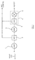
- FIG. 1 of the accompanying drawings illustrates a typical IF strip of such a known type of receiver.
- the IF signal from the front end is supplied via a first surface acoustic wave (SAW) filter 1 to a first automatic gain control amplifier 2.
- the output of the amplifier 2 is supplied via a further SAW filter 3 to a down-converter 4 comprising a second automatic gain controller amplifier 5 and a frequency changer 6.
- the frequency changer 6 converts the signal to an NZIF signal, which is typically supplied to a digital demodulator.
- the gains of the amplifiers 2 and 5 are controlled by an AGC control signal supplied by the demodulator.
- the two SAW filters 1 and 3 are required to attenuate the N+1 and N-1 channels by typically 70dB. This is a system requirement because, after conversion to the NZIF signal, the image channel is coincident with the N+1 or N-1 channel and may be up to 35dB above the level of the wanted channel N, which must be attenuated by at least 35dB relative to the channel N. Thus, several stages are necessary in order to receive the required channel, filter out the unwanted channels and convert the desired channel to the NZIF output signal.
- each SAW filter has an insertion loss of 20dB so that there is a total loss in the "direct" path of 40dB plus the gain of the amplifier 2 between the filters 1 and 3, which may typically be approximately 10dB.
- the ratio of direct signal to leakage signal is therefore only about 15dB. Because the leakage signal is phase-shifted with respect to the direct signal, the leakage signal effectively appears as an interfering signal which can severely disrupt reception of the desired channel.
- US 4 817 167 discloses an FM stereo receiver which comprises a single conversion zero intermediate frequency down-converter supplying in-phase and quadrature baseband signals to respective analog-digital converters.
- the converter outputs are supplied to an up-converter for converting the in-phase and quadrature signals to a near-zero intermediate frequency.
- the up-converter comprises a quadrature generator, a pair of mixers and a summer.
- Analog baseband filters and AGC circuits are provided between the down-converter and the analog-digital converters.
- GB 2 215 945 discloses digital baseband filters in the context of a zero intermediate frequency receiver.
- W091/14311 discloses a receiver formed in a single monolithic integrated circuit.
- EP 0 122 657 discloses a television receiver comprising a quadrature down-converter supplying in-phase and quadrature signals to an analog quadrature up-converter.
- the up-converter comprises mixers and a local oscillator producing quadrature outputs.
- the local oscillator comprises an amplitude and phase adjusting arrangement.
- a digital receiver comprising: an analog single-conversion zero intermediate frequency down-converter for converting a selected radio frequency channel to in-phase (I) and quadrature (Q) base band signals; first and second analog digital converters for converting the I and Q base band signals to digital I and Q base band signals; a digital up-converter for converting the digital I and Q base band signals to a near-zero intermediate frequency signal; and a digital demodulator, characterised in that the up-converter has a phase adjuster for adjusting the relative phases of the digital I and Q baseband signals and the digital demodulator has a correction signal generator for supplying a feedback signal to the phase adjuster based on bit error rate in the demodulator in order substantially to correct for quadrature phase imbalance in the analog down-converter.
- the up-converter may comprise a quadrature generator for generating quadrature local oscillator signals, first and second mixers for mixing the digital I and Q base band signals, respectively, with the quadrature local oscillator signals, and a summer for summing output signals of the first and second mixers.
- the phase adjuster may be arranged to adjust the phase of at least one of the quadrature local oscillator signals in response to the feedback signal.
- the phase adjuster may be arranged to provide an adjustable delay.
- the up-converter may be connected to the first and second analog-digital converters via first and second digital base band filters, respectively.
- the up-converter may be connected to the first and second digital base band filters via first and second digital automatic gain control circuits, respectively.
- the first and second analog digital converters may be connected to the down-converter via first and second analog base band filters, respectively.
- the first and second analog-digital converters may be connected to the first and second analog base band filters via first and second analog automatic gain control circuits, respectively.
- the down-converter may be connected to an input of the receiver via a third automatic gain control circuit.
- the receiver may be formed in a single monolithic integrated circuit.
- RF radio frequency
- DSP baseband digital signal processing
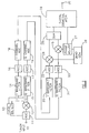
- the receiver shown in Figure 2 is intended for use as a digital terrestrial receiver but may be used in other applications.
- a receiver input 10 is connected to an RF front end in the form of an automatic gain control circuit 11 and a frequency changer 12 of the zero IF down-converter type.
- the frequency changer 12 converts the selected RF channel to base band I and Q signals which are supplied to a level detector 13 for controlling the AGC circuit 11 and to identical I and Q channels.
- the front end may be of known type and will not be described further. The quadrature balance of the front end is not critical because any imbalance is dealt with elsewhere as described hereinafter.
- the I and Q channels comprise I and Q baseband filters 14 and 15 whose outputs are supplied via analog AGC circuits 16 and 17 to simultaneously clocked analog-digital converters (ADCs) 18 and 19, respectively.
- ADCs analog-digital converters
- the outputs of the converters 18 and 19 are supplied via digital baseband filters 20 and 21 to digital AGC circuits 22 and 23, respectively.
- the outputs of the AGC circuits 22 and 23 are supplied to a digital up-converter.
- the up-converter comprises first and second mixers 24 and 25 which receive the digital I and Q baseband signals together with quadrature local oscillator signals.
- the local oscillator signals are generated by a quadrature generator 26 and one of the signals passes through a phase adjuster 27, for example providing an adjustable delay to the signal from the generator 26, controlled by a phase adjust feedback signal from a digital demodulator 29.
- the outputs of the mixers 24 and 25 are supplied to a summer 28, whose output provides an NZIF output signal to the digital demodulator 29.
- the demodulator output 30 forms the output of the receiver.
- Figure 3 illustrates the spectrum of three adjacent channels D-1, D and D+1.
- the channel D-1 occupies a band 492 to 500MHz
- the channel D occupies a band 500 to 508MHz
- the channel D+1 occupies a band from 508 to 516MHz. It is desired to receive the channel D but the power of the signal in the channel D+1 is +35dBm greater than that in the channel D.
- the local oscillator of the frequency changer 12 is set to 504MHz and the whole RF spectrum including the channels shown in Figure 3 are quadrature frequency down-converted to zero IF so that the converted channel D is centered on 0Hz.
- the frequency 508MHz is converted to +4MHz
- the frequency 500MHz is converted to -4MHz. Because of the phase characteristics of the quadrature signals, the positive and negative frequency offsets of the I channel are in phase whereas the positive and negative frequencies of the Q channel are in antiphase. This is illustrated pictorially in Figure 4.
- the level detector 13 and the AGC circuit 11 limit the amplitude of input signals to the frequency changer 12 so as to limit the generation of intermodulation products in this stage. Also, the down-conversion performed by the front end inherently introduces quadrature phase imbalances. However, these are dealt with in the digital domain as described hereinafter.
- the baseband I and Q signals are supplied to the baseband filters 14 and 15 which attenuate energy from the spectrum outside the baseband of the I and Q signals. This helps to prevent overloading of the converters 18 and 19.
- the AGC circuits 16 and 17 control the signal levels to the converters 18 and 19 following the baseband filtering.
- the converters 18 and 19 convert the baseband signals into digital baseband signals for subsequent processing in the digital domain.
- the digital filters 20 and 21 may be required because of imperfections in the filtering performed in the analog domain by the baseband filters 14 and 15.
- the AGC circuits 22 restore defined signal levels to the digital I and Q signals which are then supplied to the up-converter.
- the up-converter mixes or multiplies the digital I and Q signals with locally generated quadrature signals at 5MHz.
- the frequencies +4MHz and -4MHz are converted to 1MHz and 9MHz, respectively.
- These up-converted digital signals are vectorially summed in the summer 28 where, as illustrated, the +9MHz tones are summed and the +1MHz tones cancel each other.
- the original signal is thus reconstructed and may then be supplied to a digital demodulator (not shown).
- the demodulator supplies a phase adjust feedback correction signal to the phase adjuster 27 which compensates for phase errors in the initial down-conversion performed in the front end converter 12 and thus makes it possible to meet the quadrature crosstalk requirements of a digital receiver.
- the ADCs 18, 19 have a sampling rate of 18.26MHz.
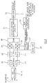
- Figure 6 also illustrates the digital demodulator 29 in more detail for the specific example of complimentary offset frequency division modulation (COFDM) signals.
- COFDM complimentary offset frequency division modulation
- other standards may be used such as ATSC or QAM.
- the digital demodulator comprises a main demodulating section 31 which, for example, performs automatic frequency control (AFC), fast Fourier transform (FFT), channel correction and timing lock.
- AFC automatic frequency control
- FFT fast Fourier transform
- the output of the section 31 is supplied to a decoder 32 which, for example, performs MPEG-2 decoding.
- the demodulator 29 also comprises a feedback signal generator in the form of a bit error rate (BER) optimisation algorithm 33 which supplies the phase adjust feedback signal to the phase adjuster 27.
- the algorithm 33 monitors the bit error rate at various stages in the decoding process, for example after the FFT or after Viterbi decoding.
- the algorithm derives from the bit error rate a correction or feedback signal which adjusts the delay provided by the phase adjuster 27 and hence varies the relative phase of the local oscillator signals supplied to the mixers 24 and 25. In particular, the relative phase is adjusted so as to minimise the bit error rate.
- BER bit error rate
- Algorithms which act to minimise a measured quantity are well known in the field of signal processing. It is thus possible substantially to correct for phase error or imbalance in the analog down-converter 12, whose quadrature performance requirements are not therefore critical to achieving an acceptable signal-to-noise ratio and hence an acceptably low bit error rate in the MPEG-2 bit stream supplied to the output 30 of the receiver.
- the receiver illustrated in Figure 2 provides improved performance compared with known receivers, such as that using the IF strip illustrated in Figure 1. Further, the receiver may be implemented in a single monolithic integrated circuit without, for example, requiring external filters. The receiver may therefore be made more compact and manufacturing cost may be substantially reduced.
Abstract
Description
- The present invention relates to a digital receiver. For example, such a receiver may be used as a digital terrestrial receiver, a digital cable receiver or in other multimedia digital receivers.
- Known types of digital receivers are based on analog techniques, for example involving single-conversion or double-conversion superheterodyne techniques. Typically, such a receiver has a final intermediate frequency (IF) in the region of 36MHz. The IF signal is further amplified and filtered and is then down-converted to a near zero intermediate frequency (NZIF). The NZIF signal is then digitised and subjected to demodulation and other processing such as forward error correction in the digital domain.
- Figure 1 of the accompanying drawings illustrates a typical IF strip of such a known type of receiver. The IF signal from the front end is supplied via a first surface acoustic wave (SAW)
filter 1 to a first automaticgain control amplifier 2. The output of theamplifier 2 is supplied via afurther SAW filter 3 to a down-converter 4 comprising a second automaticgain controller amplifier 5 and afrequency changer 6. Thefrequency changer 6 converts the signal to an NZIF signal, which is typically supplied to a digital demodulator. The gains of theamplifiers - When it is desired to receive a channel N, the two
SAW filters - The presence of two
SAW filters amplifier 2 and theconverter 4 because each filter attenuates the wanted signal by typically 20dB. These constraints may limit the signal-to-noise performance of the receiver. - The required number of stages prohibits integration of the whole receiver into a single integrated circuit, not only because of the number of stages required but also because of the requirement for two external IF SAW filters. This results from the SAW filter insertion loss of 20dB and from the finite level of isolation which may be achieved around an integrated circuit package. For example, each SAW filter has an insertion loss of 20dB so that there is a total loss in the "direct" path of 40dB plus the gain of the
amplifier 2 between thefilters - US 4 817 167 discloses an FM stereo receiver which comprises a single conversion zero intermediate frequency down-converter supplying in-phase and quadrature baseband signals to respective analog-digital converters. The converter outputs are supplied to an up-converter for converting the in-phase and quadrature signals to a near-zero intermediate frequency. The up-converter comprises a quadrature generator, a pair of mixers and a summer. Analog baseband filters and AGC circuits are provided between the down-converter and the analog-digital converters.
- GB 2 215 945 discloses digital baseband filters in the context of a zero intermediate frequency receiver.
- W091/14311 discloses a receiver formed in a single monolithic integrated circuit.
- EP 0 122 657 discloses a television receiver comprising a quadrature down-converter supplying in-phase and quadrature signals to an analog quadrature up-converter. The up-converter comprises mixers and a local oscillator producing quadrature outputs. The local oscillator comprises an amplitude and phase adjusting arrangement.
- According to the invention, there is provided a digital receiver comprising: an analog single-conversion zero intermediate frequency down-converter for converting a selected radio frequency channel to in-phase (I) and quadrature (Q) base band signals; first and second analog digital converters for converting the I and Q base band signals to digital I and Q base band signals; a digital up-converter for converting the digital I and Q base band signals to a near-zero intermediate frequency signal; and a digital demodulator, characterised in that the up-converter has a phase adjuster for adjusting the relative phases of the digital I and Q baseband signals and the digital demodulator has a correction signal generator for supplying a feedback signal to the phase adjuster based on bit error rate in the demodulator in order substantially to correct for quadrature phase imbalance in the analog down-converter.
- The up-converter may comprise a quadrature generator for generating quadrature local oscillator signals, first and second mixers for mixing the digital I and Q base band signals, respectively, with the quadrature local oscillator signals, and a summer for summing output signals of the first and second mixers.
- The phase adjuster may be arranged to adjust the phase of at least one of the quadrature local oscillator signals in response to the feedback signal.
- The phase adjuster may be arranged to provide an adjustable delay.
- The up-converter may be connected to the first and second analog-digital converters via first and second digital base band filters, respectively. The up-converter may be connected to the first and second digital base band filters via first and second digital automatic gain control circuits, respectively.
- The first and second analog digital converters may be connected to the down-converter via first and second analog base band filters, respectively. The first and second analog-digital converters may be connected to the first and second analog base band filters via first and second analog automatic gain control circuits, respectively.
- The down-converter may be connected to an input of the receiver via a third automatic gain control circuit.
- The receiver may be formed in a single monolithic integrated circuit.
- It is thus possible to provide a receiver in which the radio frequency (RF) circuitry is substantially simplified and any resulting inadequacies are overcome by increased baseband digital signal processing (DSP). Such a receiver may be implemented as or as part of a single integrated circuit, thus providing reduced size and cost while providing an improved performance compared with known digital receivers.
- The invention will be further described, by way of example, with reference to the accompanying drawings, in which:
- Figure 1 is a block circuit diagram of an IF strip of a known type of receiver;
- Figure 2 is a block circuit diagram of a digital receiver constituting an embodiment of the invention;
- Figure 3 is a diagram illustrating the spectrum of RF signals in three adjacent channels of a digital terrestrial broadcast system; and
- Figure 4 is a vector diagram of the incoming required and image signal in the I and Q channels after down conversion in the receiver of Figure 2;
- Figure 5 is a vector diagram of the required and image signals in the I and Q channels after upconversion in the receiver of Figure 2; and
- Figure 6 is a more detailed block circuit diagram of part of the receiver of Figure 2.
-
- The receiver shown in Figure 2 is intended for use as a digital terrestrial receiver but may be used in other applications. A
receiver input 10 is connected to an RF front end in the form of an automaticgain control circuit 11 and afrequency changer 12 of the zero IF down-converter type. Thefrequency changer 12 converts the selected RF channel to base band I and Q signals which are supplied to alevel detector 13 for controlling theAGC circuit 11 and to identical I and Q channels. The front end may be of known type and will not be described further. The quadrature balance of the front end is not critical because any imbalance is dealt with elsewhere as described hereinafter. - The I and Q channels comprise I and
Q baseband filters analog AGC circuits - The outputs of the
converters digital baseband filters digital AGC circuits AGC circuits - The up-converter comprises first and
second mixers quadrature generator 26 and one of the signals passes through aphase adjuster 27, for example providing an adjustable delay to the signal from thegenerator 26, controlled by a phase adjust feedback signal from adigital demodulator 29. The outputs of themixers summer 28, whose output provides an NZIF output signal to thedigital demodulator 29. Thedemodulator output 30 forms the output of the receiver. - Figure 3 illustrates the spectrum of three adjacent channels D-1, D and D+1. By way of example, the channel D-1 occupies a band 492 to 500MHz, the channel D occupies a band 500 to 508MHz and the channel D+1 occupies a band from 508 to 516MHz. It is desired to receive the channel D but the power of the signal in the channel D+1 is +35dBm greater than that in the channel D. The local oscillator of the
frequency changer 12 is set to 504MHz and the whole RF spectrum including the channels shown in Figure 3 are quadrature frequency down-converted to zero IF so that the converted channel D is centered on 0Hz. For both the I and Q components, the frequency 508MHz is converted to +4MHz and the frequency 500MHz is converted to -4MHz. Because of the phase characteristics of the quadrature signals, the positive and negative frequency offsets of the I channel are in phase whereas the positive and negative frequencies of the Q channel are in antiphase. This is illustrated pictorially in Figure 4. - The
level detector 13 and theAGC circuit 11 limit the amplitude of input signals to thefrequency changer 12 so as to limit the generation of intermodulation products in this stage. Also, the down-conversion performed by the front end inherently introduces quadrature phase imbalances. However, these are dealt with in the digital domain as described hereinafter. - The baseband I and Q signals are supplied to the baseband filters 14 and 15 which attenuate energy from the spectrum outside the baseband of the I and Q signals. This helps to prevent overloading of the
converters AGC circuits converters - The
converters digital filters AGC circuits 22 restore defined signal levels to the digital I and Q signals which are then supplied to the up-converter. - Because it is possible for a channel adjacent the selected channel to contain relatively high signal levels, for example as illustrated in Figure 3, sufficient filtering must be provided to suppress the undesired channel signals to a sufficient level below the desired signals at the inputs of the up-converter. If this can be achieved by the analog filters 14 and 15 or by filtering which may be provided in the front end, the
digital filters AGC circuits - The up-converter mixes or multiplies the digital I and Q signals with locally generated quadrature signals at 5MHz. Thus, the frequencies +4MHz and -4MHz are converted to 1MHz and 9MHz, respectively. This is illustrated in the vector diagram shown in Figure 5 which demonstrates the conversion in the I and Q channels of the +4MHz tone. These up-converted digital signals are vectorially summed in the
summer 28 where, as illustrated, the +9MHz tones are summed and the +1MHz tones cancel each other. The same happens for the -4MHz tone; in particular the +1MHz tones are summed and the +9MHz tones cancel each other. The original signal is thus reconstructed and may then be supplied to a digital demodulator (not shown). - The demodulator supplies a phase adjust feedback correction signal to the
phase adjuster 27 which compensates for phase errors in the initial down-conversion performed in thefront end converter 12 and thus makes it possible to meet the quadrature crosstalk requirements of a digital receiver. - As shown in Figure 6, the
ADCs digital demodulator 29 in more detail for the specific example of complimentary offset frequency division modulation (COFDM) signals. However, other standards may be used such as ATSC or QAM. - The digital demodulator comprises a
main demodulating section 31 which, for example, performs automatic frequency control (AFC), fast Fourier transform (FFT), channel correction and timing lock. The output of thesection 31 is supplied to adecoder 32 which, for example, performs MPEG-2 decoding. - The
demodulator 29 also comprises a feedback signal generator in the form of a bit error rate (BER)optimisation algorithm 33 which supplies the phase adjust feedback signal to thephase adjuster 27. Thealgorithm 33 monitors the bit error rate at various stages in the decoding process, for example after the FFT or after Viterbi decoding. The algorithm derives from the bit error rate a correction or feedback signal which adjusts the delay provided by thephase adjuster 27 and hence varies the relative phase of the local oscillator signals supplied to themixers converter 12, whose quadrature performance requirements are not therefore critical to achieving an acceptable signal-to-noise ratio and hence an acceptably low bit error rate in the MPEG-2 bit stream supplied to theoutput 30 of the receiver. - The receiver illustrated in Figure 2 provides improved performance compared with known receivers, such as that using the IF strip illustrated in Figure 1. Further, the receiver may be implemented in a single monolithic integrated circuit without, for example, requiring external filters. The receiver may therefore be made more compact and manufacturing cost may be substantially reduced.
Claims (10)
- A digital receiver comprising: an analog single conversion zero intermediate frequency down-converter (12) for converting a selected radio frequency channel to in-phase (I) and quadrature (Q) baseband signals; first and second analog-digital converters (18, 19) for converting the I and Q baseband signals to digital I and Q baseband signals; a digital up-converter (24-28) for converting the digital I and Q baseband signals to a near-zero intermediate frequency signal; and a digital demodulator (29), characterised in that the up-converter (24-28) has a phase adjuster (27) for adjusting the relative phase of the digital I and Q baseband signals and the digital demodulator (29) has a correction signal generator (33) for supplying a feedback signal to the phase adjuster (27) based on bit error rate in the demodulator (29) in order substantially to correct for quadrature phase imbalance in the analog down-converter (12).
- A receiver as claimed in claim 1, characterised in that the up-converter (24-28) comprises a quadrature generator (26) for generating quadrature local oscillator signals, first and second mixers (24, 25) for mixing the digital I and Q baseband signals, respectively, with the quadrature local oscillator signals, and a summer (28) for summing output signals of the first and second mixers.
- A receiver as claimed in claim 2, characterised in that the phase adjuster (27) is arranged to adjust the phase of at least one of the quadrature local oscillator signals in response to the feedback signal.
- A receiver as claimed in any one of the preceding claims, characterised in that the phase adjuster (27) is arranged to provide an adjustable delay.
- A receiver as claimed in any one of the preceding claims, characterised in that the up-converter (24-28) is connected to the first and second analog-digital converters (18, 19) via first and second digital baseband filters (20, 21), respectively.
- A receiver as claimed in claim 5, characterised in that the up-converter (24-28) is connected to the first and second digital baseband filters (20, 21) via first and second digital automatic gain control circuits (22, 23), respectively.
- A receiver as claimed in any one of the preceding claims, characterised in that the first and second analog-digital converters (18, 19) are connected to the down-converter (12) via first and second analog baseband filters (14, 15), respectively.
- A receiver as claimed in claim 7, characterised in that the first and second analog-digital converters (18, 19) are connected to the first and second analog baseband filters (14, 15) via first and second analog automatic gain control circuits (16, 17), respectively.
- A receiver as claimed in any one of the preceding claims, characterised in that the down-converter (12) is connected to an input (10) of the receiver via a third automatic gain control circuit (11).
- A receiver as claimed in any one of the preceding claims, formed in a single monolithic integrated circuit.
Applications Claiming Priority (2)
| Application Number | Priority Date | Filing Date | Title |
|---|---|---|---|
| GBGB9921811.7A GB9921811D0 (en) | 1999-09-16 | 1999-09-16 | Digital tuner |
| GB9921811 | 1999-09-16 |
Publications (3)
| Publication Number | Publication Date |
|---|---|
| EP1085665A2 true EP1085665A2 (en) | 2001-03-21 |
| EP1085665A3 EP1085665A3 (en) | 2003-06-11 |
| EP1085665B1 EP1085665B1 (en) | 2005-07-13 |
Family
ID=10860966
Family Applications (1)
| Application Number | Title | Priority Date | Filing Date |
|---|---|---|---|
| EP00307800A Expired - Lifetime EP1085665B1 (en) | 1999-09-16 | 2000-09-08 | Digital receiver |
Country Status (3)
| Country | Link |
|---|---|
| EP (1) | EP1085665B1 (en) |
| DE (1) | DE60021237D1 (en) |
| GB (1) | GB9921811D0 (en) |
Cited By (3)
| Publication number | Priority date | Publication date | Assignee | Title |
|---|---|---|---|---|
| US6973297B1 (en) | 1999-09-01 | 2005-12-06 | Sirific Wireless Corporation | Method and apparatus for down-conversion of radio frequency (RF) signals with reduced local oscillator leakage |
| GB2394373B (en) * | 2002-10-19 | 2005-12-14 | Zarlink Semiconductor Ltd | Radio frequency tuner |
| CN111711475A (en) * | 2020-06-15 | 2020-09-25 | 上海航天电子有限公司 | Polarization diversity reception method for wireless telemetry |
Citations (9)
| Publication number | Priority date | Publication date | Assignee | Title |
|---|---|---|---|---|
| EP0122657A1 (en) * | 1983-04-01 | 1984-10-24 | Koninklijke Philips Electronics N.V. | Receiver for RF signals comprising a pair of parallel signal paths |
| EP0237590A1 (en) * | 1986-03-15 | 1987-09-23 | Deutsche ITT Industries GmbH | Control circuit for controlling two signals out of phase by about 90o |
| US4817167A (en) * | 1986-08-07 | 1989-03-28 | Deutsche Itt Industries Gmbh | Method of receiving frequency-modulated stereo multiplex signals |
| GB2215945A (en) * | 1988-03-26 | 1989-09-27 | Stc Plc | Digital direct conversion radio |
| WO1991014311A1 (en) * | 1990-03-07 | 1991-09-19 | At&E Corporation | Zero if radio receiver for intermittent operation |
| EP0624033A2 (en) * | 1993-05-07 | 1994-11-09 | Koninklijke Philips Electronics N.V. | QAM television transmission system |
| US5835165A (en) * | 1995-06-07 | 1998-11-10 | Lsi Logic Corporation | Reduction of false locking code words in concatenated decoders |
| US5896061A (en) * | 1992-10-29 | 1999-04-20 | Sican Gesellschaft Fur Silizium-Anwendungen Und Cad/Cat | Homodyne receiver and process for correcting the converted received signal |
| US5937341A (en) * | 1996-09-13 | 1999-08-10 | University Of Washington | Simplified high frequency tuner and tuning method |
-
1999
- 1999-09-16 GB GBGB9921811.7A patent/GB9921811D0/en not_active Ceased
-
2000
- 2000-09-08 EP EP00307800A patent/EP1085665B1/en not_active Expired - Lifetime
- 2000-09-08 DE DE60021237T patent/DE60021237D1/en not_active Expired - Lifetime
Patent Citations (9)
| Publication number | Priority date | Publication date | Assignee | Title |
|---|---|---|---|---|
| EP0122657A1 (en) * | 1983-04-01 | 1984-10-24 | Koninklijke Philips Electronics N.V. | Receiver for RF signals comprising a pair of parallel signal paths |
| EP0237590A1 (en) * | 1986-03-15 | 1987-09-23 | Deutsche ITT Industries GmbH | Control circuit for controlling two signals out of phase by about 90o |
| US4817167A (en) * | 1986-08-07 | 1989-03-28 | Deutsche Itt Industries Gmbh | Method of receiving frequency-modulated stereo multiplex signals |
| GB2215945A (en) * | 1988-03-26 | 1989-09-27 | Stc Plc | Digital direct conversion radio |
| WO1991014311A1 (en) * | 1990-03-07 | 1991-09-19 | At&E Corporation | Zero if radio receiver for intermittent operation |
| US5896061A (en) * | 1992-10-29 | 1999-04-20 | Sican Gesellschaft Fur Silizium-Anwendungen Und Cad/Cat | Homodyne receiver and process for correcting the converted received signal |
| EP0624033A2 (en) * | 1993-05-07 | 1994-11-09 | Koninklijke Philips Electronics N.V. | QAM television transmission system |
| US5835165A (en) * | 1995-06-07 | 1998-11-10 | Lsi Logic Corporation | Reduction of false locking code words in concatenated decoders |
| US5937341A (en) * | 1996-09-13 | 1999-08-10 | University Of Washington | Simplified high frequency tuner and tuning method |
Cited By (7)
| Publication number | Priority date | Publication date | Assignee | Title |
|---|---|---|---|---|
| US6973297B1 (en) | 1999-09-01 | 2005-12-06 | Sirific Wireless Corporation | Method and apparatus for down-conversion of radio frequency (RF) signals with reduced local oscillator leakage |
| US7016662B1 (en) | 1999-09-01 | 2006-03-21 | Sirific Wireless Corporation | Method and apparatus for up-conversion of radio frequency (RF) signals |
| US7046980B1 (en) | 1999-09-01 | 2006-05-16 | Sirific Wireless Corporation | Method and apparatus for up-and down-conversion of radio frequency (RF) signals |
| GB2394373B (en) * | 2002-10-19 | 2005-12-14 | Zarlink Semiconductor Ltd | Radio frequency tuner |
| US7266350B2 (en) | 2002-10-19 | 2007-09-04 | Intel Corporation | Radio frequency tuner |
| CN111711475A (en) * | 2020-06-15 | 2020-09-25 | 上海航天电子有限公司 | Polarization diversity reception method for wireless telemetry |
| CN111711475B (en) * | 2020-06-15 | 2023-09-01 | 上海航天电子有限公司 | Polarization diversity receiving method for wireless telemetry |
Also Published As
| Publication number | Publication date |
|---|---|
| GB9921811D0 (en) | 1999-11-17 |
| DE60021237D1 (en) | 2005-08-18 |
| EP1085665A3 (en) | 2003-06-11 |
| EP1085665B1 (en) | 2005-07-13 |
Similar Documents
| Publication | Publication Date | Title |
|---|---|---|
| JP5902430B2 (en) | Harmonic rejection receiver architecture and mixer | |
| US6400416B1 (en) | Single-chip digital cable TV/cable modem tuner IC | |
| WO2001024358A1 (en) | System and method for a single conversion tuner | |
| US20040229584A1 (en) | Telecommunications receiver and a transmitter | |
| KR100515551B1 (en) | Receiver apparatus of broadcast | |
| JP3190551B2 (en) | Multi-carrier signal processing method and apparatus | |
| JPH10303767A (en) | Receiver and operating method therefor | |
| KR100560192B1 (en) | Digital Broadcast Receiver | |
| US20050090213A1 (en) | Tuner and demodulator for analog cable television | |
| EP1158676B1 (en) | Interference reducing circuit and television broadcasting receiver | |
| US6363120B1 (en) | Apparatus and method for extending the dynamic range of a mixer using feed forward distortion reduction | |
| EP0799523A1 (en) | Receiver circuit | |
| EP1085665B1 (en) | Digital receiver | |
| US7233368B2 (en) | Down-converter | |
| EP0903937B1 (en) | Digital television signal receiving tuner system | |
| US7065337B2 (en) | Tuner for digital terrestrial broadcast signals | |
| US7463874B2 (en) | Complex digital signal channel select filter for analog cable television | |
| US7343142B2 (en) | Tuner | |
| US20060194557A1 (en) | Tuner | |
| JP2002359569A (en) | Broadcasting receiver | |
| JPH10313261A (en) | Interference wave suppression circuit, interference wave suppression method and radio receiver | |
| JP2002335174A (en) | Receiver for digital broadcasting | |
| KR20030006574A (en) | Dc offset removal circuit | |
| JPH0965236A (en) | Digital broadcast receiver | |
| MXPA98002517A (en) | Signal resolutor of |
Legal Events
| Date | Code | Title | Description |
|---|---|---|---|
| PUAI | Public reference made under article 153(3) epc to a published international application that has entered the european phase |
Free format text: ORIGINAL CODE: 0009012 |
|
| AK | Designated contracting states |
Kind code of ref document: A2 Designated state(s): AT BE CH CY DE DK ES FI FR GB GR IE IT LI LU MC NL PT SE |
|
| AX | Request for extension of the european patent |
Free format text: AL;LT;LV;MK;RO;SI |
|
| RAP1 | Party data changed (applicant data changed or rights of an application transferred) |
Owner name: ZARLINK SEMICONDUCTOR LIMITED |
|
| PUAL | Search report despatched |
Free format text: ORIGINAL CODE: 0009013 |
|
| AK | Designated contracting states |
Designated state(s): AT BE CH CY DE DK ES FI FR GB GR IE IT LI LU MC NL PT SE |
|
| AX | Request for extension of the european patent |
Extension state: AL LT LV MK RO SI |
|
| 17P | Request for examination filed |
Effective date: 20031128 |
|
| 17Q | First examination report despatched |
Effective date: 20040116 |
|
| AKX | Designation fees paid |
Designated state(s): DE GB |
|
| GRAP | Despatch of communication of intention to grant a patent |
Free format text: ORIGINAL CODE: EPIDOSNIGR1 |
|
| GRAS | Grant fee paid |
Free format text: ORIGINAL CODE: EPIDOSNIGR3 |
|
| GRAA | (expected) grant |
Free format text: ORIGINAL CODE: 0009210 |
|
| AK | Designated contracting states |
Kind code of ref document: B1 Designated state(s): DE GB |
|
| REG | Reference to a national code |
Ref country code: GB Ref legal event code: FG4D |
|
| REF | Corresponds to: |
Ref document number: 60021237 Country of ref document: DE Date of ref document: 20050818 Kind code of ref document: P |
|
| PGFP | Annual fee paid to national office [announced via postgrant information from national office to epo] |
Ref country code: DE Payment date: 20050902 Year of fee payment: 6 |
|
| PG25 | Lapsed in a contracting state [announced via postgrant information from national office to epo] |
Ref country code: DE Free format text: LAPSE BECAUSE OF FAILURE TO SUBMIT A TRANSLATION OF THE DESCRIPTION OR TO PAY THE FEE WITHIN THE PRESCRIBED TIME-LIMIT Effective date: 20051014 |
|
| PLBE | No opposition filed within time limit |
Free format text: ORIGINAL CODE: 0009261 |
|
| STAA | Information on the status of an ep patent application or granted ep patent |
Free format text: STATUS: NO OPPOSITION FILED WITHIN TIME LIMIT |
|
| 26N | No opposition filed |
Effective date: 20060418 |
|
| REG | Reference to a national code |
Ref country code: GB Ref legal event code: 732E |
|
| PGFP | Annual fee paid to national office [announced via postgrant information from national office to epo] |
Ref country code: GB Payment date: 20120905 Year of fee payment: 13 |
|
| GBPC | Gb: european patent ceased through non-payment of renewal fee |
Effective date: 20130908 |
|
| PG25 | Lapsed in a contracting state [announced via postgrant information from national office to epo] |
Ref country code: GB Free format text: LAPSE BECAUSE OF NON-PAYMENT OF DUE FEES Effective date: 20130908 |