EP1146550A2 - Method for making interconnections in an integrated circuit - Google Patents
Method for making interconnections in an integrated circuit Download PDFInfo
- Publication number
- EP1146550A2 EP1146550A2 EP01400287A EP01400287A EP1146550A2 EP 1146550 A2 EP1146550 A2 EP 1146550A2 EP 01400287 A EP01400287 A EP 01400287A EP 01400287 A EP01400287 A EP 01400287A EP 1146550 A2 EP1146550 A2 EP 1146550A2
- Authority
- EP
- European Patent Office
- Prior art keywords
- cavity
- titanium
- track
- copper
- deposition
- Prior art date
- Legal status (The legal status is an assumption and is not a legal conclusion. Google has not performed a legal analysis and makes no representation as to the accuracy of the status listed.)
- Withdrawn
Links
Images

Classifications
-
- H—ELECTRICITY
- H01—ELECTRIC ELEMENTS
- H01L—SEMICONDUCTOR DEVICES NOT COVERED BY CLASS H10
- H01L23/00—Details of semiconductor or other solid state devices
- H01L23/52—Arrangements for conducting electric current within the device in operation from one component to another, i.e. interconnections, e.g. wires, lead frames
- H01L23/522—Arrangements for conducting electric current within the device in operation from one component to another, i.e. interconnections, e.g. wires, lead frames including external interconnections consisting of a multilayer structure of conductive and insulating layers inseparably formed on the semiconductor body
- H01L23/532—Arrangements for conducting electric current within the device in operation from one component to another, i.e. interconnections, e.g. wires, lead frames including external interconnections consisting of a multilayer structure of conductive and insulating layers inseparably formed on the semiconductor body characterised by the materials
- H01L23/53204—Conductive materials
- H01L23/53209—Conductive materials based on metals, e.g. alloys, metal silicides
- H01L23/53228—Conductive materials based on metals, e.g. alloys, metal silicides the principal metal being copper
- H01L23/53238—Additional layers associated with copper layers, e.g. adhesion, barrier, cladding layers
-
- H—ELECTRICITY
- H01—ELECTRIC ELEMENTS
- H01L—SEMICONDUCTOR DEVICES NOT COVERED BY CLASS H10
- H01L23/00—Details of semiconductor or other solid state devices
- H01L23/52—Arrangements for conducting electric current within the device in operation from one component to another, i.e. interconnections, e.g. wires, lead frames
- H01L23/522—Arrangements for conducting electric current within the device in operation from one component to another, i.e. interconnections, e.g. wires, lead frames including external interconnections consisting of a multilayer structure of conductive and insulating layers inseparably formed on the semiconductor body
- H01L23/5226—Via connections in a multilevel interconnection structure
-
- H—ELECTRICITY
- H01—ELECTRIC ELEMENTS
- H01L—SEMICONDUCTOR DEVICES NOT COVERED BY CLASS H10
- H01L2924/00—Indexing scheme for arrangements or methods for connecting or disconnecting semiconductor or solid-state bodies as covered by H01L24/00
- H01L2924/0001—Technical content checked by a classifier
- H01L2924/0002—Not covered by any one of groups H01L24/00, H01L24/00 and H01L2224/00
Definitions
- the invention relates to the manufacture of integrated circuits, and more particularly the production of metal tracks using a process of the "damascene" type, according to a name well known to man of the job.
- a damascene process can be carried out according to several variants.
- the track is made in providing a cavity in the inter-track dielectric disposed at metallization considered, then filling the cavity with a metal of filling, for example copper, after depositing in the bottom and on the sides of the cavity a conductive barrier layer, for example in tantalum nitride.
- the manufacturing of the integrated circuit also includes the deposit an encapsulation layer, typically made of silicon nitride, on the metallization level.
- This deposition is carried out conventionally at high temperature, typically at 400 ° C.
- manufacturing an integrated circuit requires other heat treatments, for example after each oxide deposition.
- small amounts of silicon can diffuse into the copper tracks from the nitride encapsulation layer of silicon. This then results in a significant increase in the resistivity of metal tracks.
- the invention aims to provide a solution to this problem and proposes a radically different solution to avoid increasing the resistance of metal tracks due to diffusion of silicon in the copper.
- the invention therefore provides a method of manufacturing a circuit integrated, including a production phase, at a metallization level predetermined, of at least one metallic track within a material dielectric interpiste, this phase of realization comprising an engraving dielectric material interoperates so as to form a cavity at the place from said track, the deposition in the cavity of a conductive barrier layer, for example in tantalum nitride, filling the cavity with copper and the deposition on the predetermined metallization level of a layer of silicon nitride.
- the phase of realization of the metal track further comprises, between the deposition step of the barrier layer and the copper filling step, a deposit of titanium on at least part of the barrier layer.
- the silicon in the silicon nitride layer diffuses in the copper tracks, under significant thermal budgets, for example greater than or equal to 400 ° C., the silicon forms with the titanium a titanium silicide TiSi 2 .
- the silicon that diffuses in copper is thus trapped by titanium, which preserves the low resistivity of copper.
- the layer of titanium hugs the walls of the cavity perfectly perfectly continuous, since its sole purpose is to extract copper from the diffused silicon (by transformation into titanium silicide). So, he it is possible to deposit this titanium with a simple spray, for example using an argon plasma which strikes a target in titanium.
- the deposition of titanium by spraying is sufficient to deposit titanium particles at the top of the cavity, this which has the advantage of being as close as possible to the layer of silicon nitride.
- non-reactive ion etching is carried out titanium deposited in the cavity, with a plasma flow perpendicular to the bottom of the cavity. This removes the titanium from the bottom of the cavity and thus avoiding the risk of an increase in the resistance of the line (track). And, this non-reactive ion etching with a plasma flow perpendicular to the bottom of the cavity, allows the titanium particles on the vertical sides of the cavity, and in particular those close to the upper edge of the cavity.
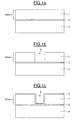
- the reference 1 designates a layer of an inter-track dielectric material, for example SiO 2 formed from ethyl tetraorthosilicate (Si (OC 2 H 5 ) 4 ; TEOS in English)). It is inside this layer 1 that the metal tracks of metallization level n will be produced.
- SiO 2 formed from ethyl tetraorthosilicate (Si (OC 2 H 5 ) 4 ; TEOS in English)
- This dielectric layer 1 rests on an encapsulation layer 2, having a thickness of the order of 120 nm, and typically made of silicon nitride SiN or more generally of Si x N y .
- This encapsulation layer 2 is deposited on a layer of an inter-level dielectric material, for example also SiO 2 formed from ethyl tetraorthosilicate, and which separates the metal level n from the lower metal level n- 1.
- This inter-level dielectric layer typically has a thickness of 800 nm.
- the next step ( Figure 1b) consists, using methods conventional photolithography, to engrave the material inter-track dielectric 1, with stop on the encapsulation layer 2, of so as to provide cavities 4 (only one of these cavities is shown on Figure 1b) at the location of future metal tracks.
- the encapsulation layer 2 serves, on the one hand to avoid contamination of the inter-level dielectric by the copper of the level n track, on the other hand of stop layer for etching of the cavity.
- a barrier layer is deposited (FIG. 1c) conductive 5, typically made of tantalum nitride or else titanium nitride.
- This layer with a thickness of a few tens of nanometers, for example 25 nm, serves as a barrier to the diffusion of copper particles in the inter-track dielectric.
- a titanium deposition is then carried out (FIG. 1d) by spraying, for example using an argon-based plasma which comes hit a titanium target at room temperature under a pressure of 1 Torr.
- the titanium particles 6 are then sprayed on the sides and the bottom of the cavity 4 as well as on the surface of the barrier layer 5.
- This cleaning step removes the titanium from the bottom of the cavity, which will avoid a risk of increasing the resistance of the track subsequent metal.
- the invention therefore has the advantage of not affecting the low resistivity of copper on metal tracks while avoiding causing damage to the integrated circuit transistors.
- the invention is not limited to the so-called variant "simple damascene" which has just been described. It also applies in particular to the variant called “self-aligned double damascene” in which simultaneously etches the cavities of the connections vertical metal (commonly known to those skilled in the art “vias”) and cavities of the future tracks of the metallization level superior.
Abstract
Le procédé comprend une phase de réalisation, à un niveau de métallisation prédéterminé, d'au moins une piste métallique 7 au sein d'un matériau diélectrique inter-pistes 1 comportant une gravure du matériau diélectrique inter-pistes 1 de façon à former une cavité 4 à l'endroit de ladite piste, le dépôt dans la cavité d'une couche-barrière conductrice 5, le remplissage de la cavité par du cuivre et le dépôt sur le niveau de métallisation prédéterminé d'une couche de nitrure de silicium 8. Entre l'étape de dépôt de la couche-barrière et l'étape de remplissage par le cuivre, on dépose du titane sur une partie au moins de la couche-barrière. Ce titane se transformera en TiSi2 (60) lors de la diffusion du silicium de la couche de nitrure de silicium 8. <IMAGE>The method comprises a phase of producing, at a predetermined metallization level, at least one metal track 7 within an inter-track dielectric material 1 comprising an etching of the inter-track dielectric material 1 so as to form a cavity 4 at the location of said track, the deposition in the cavity of a conductive barrier layer 5, the filling of the cavity with copper and the deposition on the predetermined metallization level of a layer of silicon nitride 8. Between the step of depositing the barrier layer and the step of filling with copper, titanium is deposited on at least part of the barrier layer. This titanium will transform into TiSi2 (60) during the diffusion of the silicon from the silicon nitride layer 8. <IMAGE>
Description
L'invention concerne la fabrication des circuits intégrés, et plus particulièrement la réalisation des pistes métalliques utilisant un procédé du type "damascène", selon une dénomination bien connue de l'homme du métier.The invention relates to the manufacture of integrated circuits, and more particularly the production of metal tracks using a process of the "damascene" type, according to a name well known to man of the job.
Un procédé de damascène peut être effectué selon plusieurs variantes. Dans la variante dite "simple damascène", on réalise la piste en ménageant une cavité dans le diélectrique interpiste disposé au niveau de métallisation considéré, puis en remplissant la cavité par un métal de remplissage, par exemple du cuivre, après avoir déposé dans le fond et sur les flancs de la cavité une couche-barrière conductrice, par exemple en nitrure de tantale.A damascene process can be carried out according to several variants. In the so-called "simple damascene" variant, the track is made in providing a cavity in the inter-track dielectric disposed at metallization considered, then filling the cavity with a metal of filling, for example copper, after depositing in the bottom and on the sides of the cavity a conductive barrier layer, for example in tantalum nitride.
La fabrication du circuit intégré comporte également le dépôt d'une couche d'encapsulation, typiquement en nitrure de silicium, sur le niveau de métallisation. Ce dépôt s'effectue de façon classique à haute température, typiquement à 400°C. Par ailleurs, outre ce traitement thermique, la fabrication d'un circuit intégré nécessite d'autres traitements thermiques, par exemple après chaque dépôt d'oxyde. Or, lors de ces traitements thermiques, et notamment lors du dépôt à 400°C du nitrure de silicium, de petites quantités de silicium peuvent diffuser dans les pistes en cuivre à partir de la couche d'encapsulation en nitrure de silicium. Il en résulte alors une augmentation significative de la résistivité des pistes métalliques.The manufacturing of the integrated circuit also includes the deposit an encapsulation layer, typically made of silicon nitride, on the metallization level. This deposition is carried out conventionally at high temperature, typically at 400 ° C. Furthermore, in addition to this treatment thermal, manufacturing an integrated circuit requires other heat treatments, for example after each oxide deposition. However, when of these heat treatments, and in particular during the deposition at 400 ° C. of the silicon nitride, small amounts of silicon can diffuse into the copper tracks from the nitride encapsulation layer of silicon. This then results in a significant increase in the resistivity of metal tracks.
Actuellement, cet effet indésirable sur la résistance des pistes peut être évité en exposant le niveau de métallisation à un plasma d'ammoniaque avant le dépôt de la couche d'encapsulation en nitrure de silicium. Ceci permet d'empêcher la diffusion ultérieure du silicium. Cependant, un tel traitement à base de plasma peut endommager les transistors du circuit intégré.Currently, this undesirable effect on the resistance of the tracks can be avoided by exposing the metallization level to a plasma of ammonia before the deposition of the nitride encapsulation layer of silicon. This prevents further diffusion of the silicon. However, such a plasma treatment can damage integrated circuit transistors.
L'invention vise à apporter une solution à ce problème et propose une solution radicalement différente pour éviter l'augmentation de la résistance des pistes métalliques due à une diffusion de silicium dans le cuivre.The invention aims to provide a solution to this problem and proposes a radically different solution to avoid increasing the resistance of metal tracks due to diffusion of silicon in the copper.
L'invention propose donc un procédé de fabrication d'un circuit intégré, comprenant une phase de réalisation, à un niveau de métallisation prédéterminé, d'au moins une piste métallique au sein d'un matériau diélectrique interpiste, cette phase de réalisation comportant une gravure du matériau diélectrique interpiste de façon à former une cavité à l'endroit de ladite piste, le dépôt dans la cavité d'une couche-barrière conductrice, par exemple en nitrure de tantale, le remplissage de la cavité par du cuivre et le dépôt sur le niveau de métallisation prédéterminé d'une couche de nitrure de silicium.The invention therefore provides a method of manufacturing a circuit integrated, including a production phase, at a metallization level predetermined, of at least one metallic track within a material dielectric interpiste, this phase of realization comprising an engraving dielectric material interoperates so as to form a cavity at the place from said track, the deposition in the cavity of a conductive barrier layer, for example in tantalum nitride, filling the cavity with copper and the deposition on the predetermined metallization level of a layer of silicon nitride.
Selon une caractéristique générale de l'invention, la phase de réalisation de la piste métallique comprend en outre, entre l'étape de dépôt de la couche-barrière et l'étape de remplissage par le cuivre, un dépôt de titane sur une partie au moins de la couche-barrière.According to a general characteristic of the invention, the phase of realization of the metal track further comprises, between the deposition step of the barrier layer and the copper filling step, a deposit of titanium on at least part of the barrier layer.
Ainsi, lorsque le silicium de la couche de nitrure de silicium diffuse dans les pistes en cuivre, sous des budgets thermiques importants, par exemple supérieur ou égal à 400°C, le silicium forme avec le titane un siliciure de titane TiSi2. Le silicium qui diffuse dans le cuivre est ainsi piégé par le titane, ce qui permet de préserver la basse résistivité du cuivre.Thus, when the silicon in the silicon nitride layer diffuses in the copper tracks, under significant thermal budgets, for example greater than or equal to 400 ° C., the silicon forms with the titanium a titanium silicide TiSi 2 . The silicon that diffuses in copper is thus trapped by titanium, which preserves the low resistivity of copper.
D'une façon générale, il n'est pas nécessaire que la couche de titane épouse parfaitement les parois de la cavité ni qu'elle soit parfaitement continue, puisque son seul but est d'extraire du cuivre le silicium ayant diffusé (par transformation en siliciure de titane). Ainsi, il est possible d'effectuer ce dépôt de titane par une simple pulvérisation, par exemple à l'aide d'un plasma d'argon qui vient frapper une cible en titane.In general, it is not necessary that the layer of titanium hugs the walls of the cavity perfectly perfectly continuous, since its sole purpose is to extract copper from the diffused silicon (by transformation into titanium silicide). So, he it is possible to deposit this titanium with a simple spray, for example using an argon plasma which strikes a target in titanium.
Par ailleurs, le dépôt de titane par pulvérisation s'avère suffisant pour déposer des particules de titane à la partie supérieure de la cavité, ce qui présente l'avantage d'être le plus proche possible de la couche de nitrure de silicium.Furthermore, the deposition of titanium by spraying is sufficient to deposit titanium particles at the top of the cavity, this which has the advantage of being as close as possible to the layer of silicon nitride.
Selon un mode de mise en oeuvre de l'invention, préalablement au remplissage par le cuivre, on effectue une gravure ionique non réactive du titane déposé dans la cavité, avec un flux de plasma perpendiculaire au fond de la cavité. Ceci permet de retirer le titane du fond de la cavité et d'éviter ainsi le risque d'un accroissement de la résistance de la ligne (piste). Et, cette gravure ionique non réactive avec un flux de plasma perpendiculaire au fond de la cavité, permet de laisser subsister les particules de titane sur les flancs verticaux de la cavité, et en particulier celles proches du bord supérieur de la cavité.According to an embodiment of the invention, previously when filling with copper, non-reactive ion etching is carried out titanium deposited in the cavity, with a plasma flow perpendicular to the bottom of the cavity. This removes the titanium from the bottom of the cavity and thus avoiding the risk of an increase in the resistance of the line (track). And, this non-reactive ion etching with a plasma flow perpendicular to the bottom of the cavity, allows the titanium particles on the vertical sides of the cavity, and in particular those close to the upper edge of the cavity.
D'autres avantages et caractéristiques de l'invention apparaítront à l'examen de la description détaillée d'un mode de mise en oeuvre, nullement limitatif, et des dessins annexés, sur lesquels :
- les figures 1a à 1h illustrent schématiquement un mode de mise en oeuvre du procédé selon l'invention, plus particulièrement dans le cadre d'un procédé simple damascène.
- Figures 1a to 1h schematically illustrate an embodiment of the method according to the invention, more particularly in the context of a simple damascene method.
Sur la figure 1a, la référence 1 désigne une couche d'un matériau
diélectrique inter-pistes, par exemple du SiO2 formé à partir de
tétraorthosilicate d'éthyle (Si(OC2H5)4; TEOS en langue anglaise)). C'est
à l'intérieur de cette couche 1 que l'on va réaliser les pistes métalliques du
niveau de métallisation n.In FIG. 1a, the
Cette couche diélectrique 1 repose sur une couche
d'encapsulation 2, ayant une épaisseur de l'ordre de 120 nm, et
typiquement en nitrure de silicium SiN ou plus généralement en SixNy.
Cette couche d'encapsulation 2 est déposée sur une couche d'un matériau
diélectrique inter-niveaux, par exemple également du SiO2 formé à partir
de tétraorthosilicate d'éthyle, et qui sépare le niveau de métal n du niveau
de métal inférieur n-1. Cette couche de diélectrique inter-niveaux a
typiquement une épaisseur de 800 nm.This
L'étape suivante (figure 1b) consiste, en utilisant des méthodes
classiques de photo-lithographie, à effectuer une gravure du matériau
diélectrique inter-pistes 1, avec arrêt sur la couche d'encapsulation 2, de
façon à ménager des cavités 4 (une seule de ces cavités est représentée sur
la figure 1b) à l'endroit des futures pistes métalliques. The next step (Figure 1b) consists, using methods
conventional photolithography, to engrave the material
inter-track dielectric 1, with stop on the
Il convient de noter ici que la couche d'encapsulation 2 sert,
d'une part à éviter une contamination du diélectrique inter-niveaux par le
cuivre de la piste du niveau n, d'autre part de couche d'arrêt pour la gravure
de la cavité.It should be noted here that the
On dépose ensuite (figure 1c), de façon classique, une couche-barrière conductrice 5, typiquement en nitrure de tantale ou bien en nitrure de titane. Cette couche, d'une épaisseur de quelques dizaines de nanomètres, par exemple 25 nm, sert de barrière à la diffusion de particules de cuivre dans le diélectrique inter-pistes.Next, a barrier layer is deposited (FIG. 1c) conductive 5, typically made of tantalum nitride or else titanium nitride. This layer, with a thickness of a few tens of nanometers, for example 25 nm, serves as a barrier to the diffusion of copper particles in the inter-track dielectric.
On effectue ensuite (figure 1d) un dépôt de titane par
pulvérisation, par exemple en utilisant un plasma à base d'argon qui vient
frapper une cible en titane à température ambiante sous une pression de 1
Torr. Les particules de titane 6 sont alors pulvérisées sur les flancs et le
fond de la cavité 4 ainsi que sur la surface de la couche-barrière 5.A titanium deposition is then carried out (FIG. 1d) by
spraying, for example using an argon-based plasma which comes
hit a titanium target at room temperature under a pressure of 1
Torr. The
Quoique non indispensable, on effectue ensuite
avantageusement (figure 1e) une gravure ionique non réactive du titane 6
pulvérisé à l'étape précédente, de façon à retirer les particules de titane
notamment dans le fond de la cavité. Cette gravure ionique non réactive a
également pour conséquence de retirer le titane sur la surface supérieure
de la couche-barrière 5. Une telle gravure ionique non réactive est
classique pour l'homme du métier. Elle s'effectue ainsi typiquement avec
un flux d'ions dirigé perpendiculairement au fond de la cavité 4.Although not essential, we then perform
advantageously (FIG. 1e) non-reactive ion etching of
Cette étape de nettoyage permet de retirer le titane du fond de la cavité, ce qui évitera un risque d'accroissement de la résistance de la piste métallique ultérieure.This cleaning step removes the titanium from the bottom of the cavity, which will avoid a risk of increasing the resistance of the track subsequent metal.
On procède ensuite (figure 1f) à un dépôt classique de cuivre 7,
puis on effectue un polissage mécano-chimique classique de façon à
obtenir la configuration illustrée sur la figure 1g. Ce polissage permet
également avantageusement de retirer des résidus éventuels de titane, qui
auraient pu subsister après la gravure ionique non réactive du titane.We then proceed (FIG. 1f) to a
On procède ensuite (figure 1h) au dépôt d'une autre couche
d'encapsulation 8 en nitrure de silicium. Ce dépôt s'effectue
classiquement sous un budget thermique de l'ordre de 400°C, ce qui
provoque une diffusion de silicium dans le cuivre de la cavité 4.
Cependant, le silicium ainsi diffusé est piégé par les particules de titane et
se transforme en un siliciure de titane TiSi2 60, ce qui permet de préserver
la faible résistivité du cuivre.We then proceed (Figure 1h) to deposit another
L'invention présente donc l'avantage de ne pas affecter la faible résistivité du cuivre des pistes métalliques tout en évitant de causer des dommages aux transistors du circuit intégré.The invention therefore has the advantage of not affecting the low resistivity of copper on metal tracks while avoiding causing damage to the integrated circuit transistors.
Bien entendu, l'invention n'est pas limitée à la variante dite "simple damascène" qui vient d'être décrite. Elle s'applique également notamment à la variante dite "double damascène auto-aligné" dans laquelle on réalise simultanément la gravure des cavités des connexions métalliques verticales (communément appelées par l'homme du métier "vias") et des cavités des futures pistes du niveau de métallisation supérieur.Of course, the invention is not limited to the so-called variant "simple damascene" which has just been described. It also applies in particular to the variant called "self-aligned double damascene" in which simultaneously etches the cavities of the connections vertical metal (commonly known to those skilled in the art "vias") and cavities of the future tracks of the metallization level superior.
Claims (3)
Applications Claiming Priority (2)
| Application Number | Priority Date | Filing Date | Title |
|---|---|---|---|
| FR0001801A FR2805084B1 (en) | 2000-02-14 | 2000-02-14 | METHOD FOR MANUFACTURING METAL TRACKS FOR INTEGRATED CIRCUITS |
| FR0001801 | 2000-02-14 |
Publications (2)
| Publication Number | Publication Date |
|---|---|
| EP1146550A2 true EP1146550A2 (en) | 2001-10-17 |
| EP1146550A3 EP1146550A3 (en) | 2002-01-16 |
Family
ID=8846973
Family Applications (1)
| Application Number | Title | Priority Date | Filing Date |
|---|---|---|---|
| EP01400287A Withdrawn EP1146550A3 (en) | 2000-02-14 | 2001-02-06 | Method for making interconnections in an integrated circuit |
Country Status (4)
| Country | Link |
|---|---|
| US (1) | US6528419B1 (en) |
| EP (1) | EP1146550A3 (en) |
| JP (1) | JP2001230257A (en) |
| FR (1) | FR2805084B1 (en) |
Families Citing this family (6)
| Publication number | Priority date | Publication date | Assignee | Title |
|---|---|---|---|---|
| JP4447438B2 (en) * | 2004-11-29 | 2010-04-07 | Necエレクトロニクス株式会社 | Manufacturing method of semiconductor device |
| JP2010503191A (en) * | 2006-09-04 | 2010-01-28 | コーニンクレッカ フィリップス エレクトロニクス エヌ ヴィ | Controlling carbon nanostructure growth in interconnected structures |
| US8143157B2 (en) * | 2006-11-29 | 2012-03-27 | Nxp B.V. | Fabrication of a diffusion barrier cap on copper containing conductive elements |
| US7964934B1 (en) | 2007-05-22 | 2011-06-21 | National Semiconductor Corporation | Fuse target and method of forming the fuse target in a copper process flow |
| US8030733B1 (en) | 2007-05-22 | 2011-10-04 | National Semiconductor Corporation | Copper-compatible fuse target |
| US7709956B2 (en) * | 2008-09-15 | 2010-05-04 | National Semiconductor Corporation | Copper-topped interconnect structure that has thin and thick copper traces and method of forming the copper-topped interconnect structure |
Citations (4)
| Publication number | Priority date | Publication date | Assignee | Title |
|---|---|---|---|---|
| EP0552968A2 (en) * | 1992-01-23 | 1993-07-28 | Samsung Electronics Co. Ltd. | Semiconductor device including a wiring layer |
| US5595937A (en) * | 1995-04-13 | 1997-01-21 | Nec Corporation | Method for fabricating semiconductor device with interconnections buried in trenches |
| US5821168A (en) * | 1997-07-16 | 1998-10-13 | Motorola, Inc. | Process for forming a semiconductor device |
| DE19814703A1 (en) * | 1997-07-16 | 1999-01-28 | Mitsubishi Electric Corp | Filling semiconductor device trench and-or via with copper |
Family Cites Families (8)
| Publication number | Priority date | Publication date | Assignee | Title |
|---|---|---|---|---|
| JPH11145138A (en) * | 1997-11-10 | 1999-05-28 | Hitachi Ltd | Semiconductor device and manufacture thereof |
| JP3500564B2 (en) * | 1997-12-19 | 2004-02-23 | 富士通株式会社 | Method for manufacturing semiconductor device |
| US6218302B1 (en) * | 1998-07-21 | 2001-04-17 | Motorola Inc. | Method for forming a semiconductor device |
| US6093632A (en) * | 1998-12-07 | 2000-07-25 | Industrial Technology Research Institute | Modified dual damascene process |
| US6225210B1 (en) * | 1998-12-09 | 2001-05-01 | Advanced Micro Devices, Inc. | High density capping layers with improved adhesion to copper interconnects |
| US6258707B1 (en) * | 1999-01-07 | 2001-07-10 | International Business Machines Corporation | Triple damascence tungsten-copper interconnect structure |
| US6100181A (en) * | 1999-05-05 | 2000-08-08 | Advanced Micro Devices, Inc. | Low dielectric constant coating of conductive material in a damascene process for semiconductors |
| US6197681B1 (en) * | 1999-12-31 | 2001-03-06 | United Microelectronics Corp. | Forming copper interconnects in dielectric materials with low constant dielectrics |
-
2000
- 2000-02-14 FR FR0001801A patent/FR2805084B1/en not_active Expired - Fee Related
-
2001
- 2001-02-06 EP EP01400287A patent/EP1146550A3/en not_active Withdrawn
- 2001-02-07 JP JP2001031574A patent/JP2001230257A/en active Pending
- 2001-02-21 US US09/790,259 patent/US6528419B1/en not_active Expired - Fee Related
Patent Citations (4)
| Publication number | Priority date | Publication date | Assignee | Title |
|---|---|---|---|---|
| EP0552968A2 (en) * | 1992-01-23 | 1993-07-28 | Samsung Electronics Co. Ltd. | Semiconductor device including a wiring layer |
| US5595937A (en) * | 1995-04-13 | 1997-01-21 | Nec Corporation | Method for fabricating semiconductor device with interconnections buried in trenches |
| US5821168A (en) * | 1997-07-16 | 1998-10-13 | Motorola, Inc. | Process for forming a semiconductor device |
| DE19814703A1 (en) * | 1997-07-16 | 1999-01-28 | Mitsubishi Electric Corp | Filling semiconductor device trench and-or via with copper |
Also Published As
| Publication number | Publication date |
|---|---|
| EP1146550A3 (en) | 2002-01-16 |
| FR2805084B1 (en) | 2003-09-26 |
| FR2805084A1 (en) | 2001-08-17 |
| JP2001230257A (en) | 2001-08-24 |
| US6528419B1 (en) | 2003-03-04 |
Similar Documents
| Publication | Publication Date | Title |
|---|---|---|
| EP0351001B1 (en) | Method for making a semi-conductor device with at least one level of interconnection with small dimensioned via holes | |
| US5147819A (en) | Semiconductor metallization method | |
| EP0325808B1 (en) | Process for producing an electric connexion on a silicon semiconductor device | |
| JP3006735B2 (en) | Semiconductor device and manufacturing method thereof | |
| EP0343698B1 (en) | Process for producing interconnect structures on a semiconductor device, especially on an LSI circuit | |
| US6334249B2 (en) | Cavity-filling method for reducing surface topography and roughness | |
| FR2757312A1 (en) | SELF-ALIGNED METAL GRID TRANSISTOR AND MANUFACTURING METHOD THEREOF | |
| JPH06216263A (en) | Wiring layer formation of semiconductor device | |
| EP0143700A2 (en) | Process for making integrated circuits having connectors comprising tantalum silicides, and integrated circuits made by this process | |
| US5985751A (en) | Process for fabricating interconnection of semiconductor device | |
| JP2001085438A (en) | Method for forming copper interconnection during manufacture of ic device | |
| FR2764734A1 (en) | METHOD FOR FORMING CONTACT PLATES OF A SEMICONDUCTOR DEVICE | |
| EP1480266A2 (en) | Process of making integrated electronic circuit with stacked elements and corresponding integrated electronic circuit. | |
| EP1146550A2 (en) | Method for making interconnections in an integrated circuit | |
| FR3000840A1 (en) | METHOD FOR MAKING METAL CONTACTS WITHIN AN INTEGRATED CIRCUIT, AND CORRESPONDING INTEGRATED CIRCUIT | |
| FR2763424A1 (en) | Dual damascene process for integrated circuits | |
| EP1463102A2 (en) | Method of manufacturing a transistor with metal gate and corresponding transistor | |
| EP1650796A2 (en) | Process for a contact plug on a region of an integrated circuit, in particular on the electrodes of a transistor | |
| WO2004057658A2 (en) | Mis transistor with self-aligned gate and method for making same | |
| FR2782841A1 (en) | PROCESS FOR FORMING CONTACT PLATES AND, AT THE SAME TIME, TO PLANE A SURFACE OF SUBSTRATE IN INTEGRATED CIRCUITS | |
| US5994213A (en) | Aluminum plug process | |
| EP3072148B1 (en) | Method of protecting a silicide layer | |
| FR3037714A1 (en) | METHOD FOR MAKING A CONTACT ON AN ACTIVE ZONE OF AN INTEGRATED CIRCUIT, FOR EXAMPLE ON A SOI SUBSTRATE, IN PARTICULAR FDSOI, AND INTEGRATED CIRCUIT CORRESPONDING | |
| FR2713397A1 (en) | Process for forming thin and thick metallic layers. | |
| KR20070082887A (en) | Semiconductor device and method of manufacturing the same |
Legal Events
| Date | Code | Title | Description |
|---|---|---|---|
| PUAI | Public reference made under article 153(3) epc to a published international application that has entered the european phase |
Free format text: ORIGINAL CODE: 0009012 |
|
| AK | Designated contracting states |
Kind code of ref document: A2 Designated state(s): AT BE CH CY DE DK ES FI FR GB GR IE IT LI LU MC NL PT SE TR Kind code of ref document: A2 Designated state(s): DE FR GB IT |
|
| AX | Request for extension of the european patent |
Free format text: AL;LT;LV;MK;RO;SI |
|
| PUAL | Search report despatched |
Free format text: ORIGINAL CODE: 0009013 |
|
| RAP1 | Party data changed (applicant data changed or rights of an application transferred) |
Owner name: KONINKLIJKE PHILIPS ELECTRONICS N.V. Owner name: STMICROELECTRONICS S.A. |
|
| AK | Designated contracting states |
Kind code of ref document: A3 Designated state(s): AT BE CH CY DE DK ES FI FR GB GR IE IT LI LU MC NL PT SE TR |
|
| AX | Request for extension of the european patent |
Free format text: AL;LT;LV;MK;RO;SI |
|
| 17P | Request for examination filed |
Effective date: 20020708 |
|
| AKX | Designation fees paid |
Free format text: DE FR GB IT |
|
| 17Q | First examination report despatched |
Effective date: 20071009 |
|
| RAP1 | Party data changed (applicant data changed or rights of an application transferred) |
Owner name: NXP B.V. Owner name: STMICROELECTRONICS S.A. |
|
| STAA | Information on the status of an ep patent application or granted ep patent |
Free format text: STATUS: THE APPLICATION IS DEEMED TO BE WITHDRAWN |
|
| 18D | Application deemed to be withdrawn |
Effective date: 20141209 |