EP1163544B1 - method of making ultraviolet filters with enhanced weatherability - Google Patents
method of making ultraviolet filters with enhanced weatherability Download PDFInfo
- Publication number
- EP1163544B1 EP1163544B1 EP00910092A EP00910092A EP1163544B1 EP 1163544 B1 EP1163544 B1 EP 1163544B1 EP 00910092 A EP00910092 A EP 00910092A EP 00910092 A EP00910092 A EP 00910092A EP 1163544 B1 EP1163544 B1 EP 1163544B1
- Authority
- EP
- European Patent Office
- Prior art keywords
- layer
- target
- plasma
- zinc oxide
- substrate
- Prior art date
- Legal status (The legal status is an assumption and is not a legal conclusion. Google has not performed a legal analysis and makes no representation as to the accuracy of the status listed.)
- Expired - Lifetime
Links
- 238000004519 manufacturing process Methods 0.000 title description 8
- 239000000758 substrate Substances 0.000 claims abstract description 76
- 238000004544 sputter deposition Methods 0.000 claims abstract description 24
- 238000000576 coating method Methods 0.000 claims abstract description 17
- 239000011248 coating agent Substances 0.000 claims abstract description 14
- XLOMVQKBTHCTTD-UHFFFAOYSA-N Zinc monoxide Chemical compound [Zn]=O XLOMVQKBTHCTTD-UHFFFAOYSA-N 0.000 claims description 116
- 239000011787 zinc oxide Substances 0.000 claims description 58
- 230000003287 optical effect Effects 0.000 claims description 51
- 229910052738 indium Inorganic materials 0.000 claims description 50
- 239000000376 reactant Substances 0.000 claims description 48
- APFVFJFRJDLVQX-UHFFFAOYSA-N indium atom Chemical compound [In] APFVFJFRJDLVQX-UHFFFAOYSA-N 0.000 claims description 46
- 239000011701 zinc Substances 0.000 claims description 39
- 239000007789 gas Substances 0.000 claims description 34
- 238000000034 method Methods 0.000 claims description 29
- 229910052725 zinc Inorganic materials 0.000 claims description 25
- XKRFYHLGVUSROY-UHFFFAOYSA-N Argon Chemical compound [Ar] XKRFYHLGVUSROY-UHFFFAOYSA-N 0.000 claims description 24
- HCHKCACWOHOZIP-UHFFFAOYSA-N Zinc Chemical compound [Zn] HCHKCACWOHOZIP-UHFFFAOYSA-N 0.000 claims description 20
- 238000005299 abrasion Methods 0.000 claims description 19
- 238000001755 magnetron sputter deposition Methods 0.000 claims description 19
- VYPSYNLAJGMNEJ-UHFFFAOYSA-N Silicium dioxide Chemical compound O=[Si]=O VYPSYNLAJGMNEJ-UHFFFAOYSA-N 0.000 claims description 17
- 229910052786 argon Inorganic materials 0.000 claims description 12
- 239000004417 polycarbonate Substances 0.000 claims description 10
- 229920000515 polycarbonate Polymers 0.000 claims description 10
- 239000000377 silicon dioxide Substances 0.000 claims description 7
- 235000012239 silicon dioxide Nutrition 0.000 claims description 6
- 239000004697 Polyetherimide Substances 0.000 claims description 3
- -1 polyestercarbonate Polymers 0.000 claims description 3
- 229920001601 polyetherimide Polymers 0.000 claims description 3
- PNEYBMLMFCGWSK-UHFFFAOYSA-N aluminium oxide Inorganic materials [O-2].[O-2].[O-2].[Al+3].[Al+3] PNEYBMLMFCGWSK-UHFFFAOYSA-N 0.000 claims description 2
- 239000004695 Polyether sulfone Substances 0.000 claims 1
- 229920006393 polyether sulfone Polymers 0.000 claims 1
- 238000000151 deposition Methods 0.000 abstract description 22
- 230000008021 deposition Effects 0.000 abstract description 17
- 229910044991 metal oxide Inorganic materials 0.000 abstract description 13
- 150000004706 metal oxides Chemical class 0.000 abstract description 13
- 230000005855 radiation Effects 0.000 abstract description 6
- 239000010410 layer Substances 0.000 description 135
- 238000012360 testing method Methods 0.000 description 47
- 229910052751 metal Inorganic materials 0.000 description 38
- 239000002184 metal Substances 0.000 description 38
- XLYOFNOQVPJJNP-UHFFFAOYSA-N water Substances O XLYOFNOQVPJJNP-UHFFFAOYSA-N 0.000 description 34
- QVGXLLKOCUKJST-UHFFFAOYSA-N atomic oxygen Chemical compound [O] QVGXLLKOCUKJST-UHFFFAOYSA-N 0.000 description 20
- 229910052760 oxygen Inorganic materials 0.000 description 20
- 239000001301 oxygen Substances 0.000 description 20
- 238000010521 absorption reaction Methods 0.000 description 18
- GWEVSGVZZGPLCZ-UHFFFAOYSA-N Titan oxide Chemical compound O=[Ti]=O GWEVSGVZZGPLCZ-UHFFFAOYSA-N 0.000 description 16
- 229910052782 aluminium Inorganic materials 0.000 description 16
- 239000011521 glass Substances 0.000 description 15
- XAGFODPZIPBFFR-UHFFFAOYSA-N aluminium Chemical compound [Al] XAGFODPZIPBFFR-UHFFFAOYSA-N 0.000 description 14
- 229910052739 hydrogen Inorganic materials 0.000 description 14
- 239000000463 material Substances 0.000 description 14
- 230000003247 decreasing effect Effects 0.000 description 12
- 239000000523 sample Substances 0.000 description 10
- 239000010408 film Substances 0.000 description 9
- GQPLMRYTRLFLPF-UHFFFAOYSA-N Nitrous Oxide Chemical compound [O-][N+]#N GQPLMRYTRLFLPF-UHFFFAOYSA-N 0.000 description 8
- 238000002474 experimental method Methods 0.000 description 8
- JLTRXTDYQLMHGR-UHFFFAOYSA-N trimethylaluminium Chemical compound C[Al](C)C JLTRXTDYQLMHGR-UHFFFAOYSA-N 0.000 description 8
- 125000004429 atom Chemical group 0.000 description 7
- 239000002019 doping agent Substances 0.000 description 7
- 239000000203 mixture Substances 0.000 description 7
- 229920000642 polymer Polymers 0.000 description 7
- 238000005546 reactive sputtering Methods 0.000 description 7
- 230000007423 decrease Effects 0.000 description 6
- AXAZMDOAUQTMOW-UHFFFAOYSA-N dimethylzinc Chemical compound C[Zn]C AXAZMDOAUQTMOW-UHFFFAOYSA-N 0.000 description 6
- 238000010438 heat treatment Methods 0.000 description 6
- 239000007787 solid Substances 0.000 description 6
- OTRPZROOJRIMKW-UHFFFAOYSA-N triethylindigane Chemical compound CC[In](CC)CC OTRPZROOJRIMKW-UHFFFAOYSA-N 0.000 description 6
- 239000011229 interlayer Substances 0.000 description 5
- WFKWXMTUELFFGS-UHFFFAOYSA-N tungsten Chemical compound [W] WFKWXMTUELFFGS-UHFFFAOYSA-N 0.000 description 5
- IJGRMHOSHXDMSA-UHFFFAOYSA-N Atomic nitrogen Chemical compound N#N IJGRMHOSHXDMSA-UHFFFAOYSA-N 0.000 description 4
- BVKZGUZCCUSVTD-UHFFFAOYSA-L Carbonate Chemical compound [O-]C([O-])=O BVKZGUZCCUSVTD-UHFFFAOYSA-L 0.000 description 4
- 238000002835 absorbance Methods 0.000 description 4
- IISBACLAFKSPIT-UHFFFAOYSA-N bisphenol A Chemical compound C=1C=C(O)C=CC=1C(C)(C)C1=CC=C(O)C=C1 IISBACLAFKSPIT-UHFFFAOYSA-N 0.000 description 4
- 230000008020 evaporation Effects 0.000 description 4
- 238000001704 evaporation Methods 0.000 description 4
- 239000001272 nitrous oxide Substances 0.000 description 4
- 239000000126 substance Substances 0.000 description 4
- 229910052721 tungsten Inorganic materials 0.000 description 4
- 239000010937 tungsten Substances 0.000 description 4
- RYGMFSIKBFXOCR-UHFFFAOYSA-N Copper Chemical compound [Cu] RYGMFSIKBFXOCR-UHFFFAOYSA-N 0.000 description 3
- KFZMGEQAYNKOFK-UHFFFAOYSA-N Isopropanol Chemical compound CC(C)O KFZMGEQAYNKOFK-UHFFFAOYSA-N 0.000 description 3
- 239000006096 absorbing agent Substances 0.000 description 3
- 238000006243 chemical reaction Methods 0.000 description 3
- 238000004140 cleaning Methods 0.000 description 3
- 229910052802 copper Inorganic materials 0.000 description 3
- 239000010949 copper Substances 0.000 description 3
- 238000010894 electron beam technology Methods 0.000 description 3
- UQEAIHBTYFGYIE-UHFFFAOYSA-N hexamethyldisiloxane Chemical compound C[Si](C)(C)O[Si](C)(C)C UQEAIHBTYFGYIE-UHFFFAOYSA-N 0.000 description 3
- 238000002347 injection Methods 0.000 description 3
- 239000007924 injection Substances 0.000 description 3
- 238000010926 purge Methods 0.000 description 3
- 238000001552 radio frequency sputter deposition Methods 0.000 description 3
- 229910052814 silicon oxide Inorganic materials 0.000 description 3
- 229910052709 silver Inorganic materials 0.000 description 3
- UHUUYVZLXJHWDV-UHFFFAOYSA-N trimethyl(methylsilyloxy)silane Chemical compound C[SiH2]O[Si](C)(C)C UHUUYVZLXJHWDV-UHFFFAOYSA-N 0.000 description 3
- 229910052724 xenon Inorganic materials 0.000 description 3
- FHNFHKCVQCLJFQ-UHFFFAOYSA-N xenon atom Chemical compound [Xe] FHNFHKCVQCLJFQ-UHFFFAOYSA-N 0.000 description 3
- ZSLUVFAKFWKJRC-IGMARMGPSA-N 232Th Chemical compound [232Th] ZSLUVFAKFWKJRC-IGMARMGPSA-N 0.000 description 2
- QGZKDVFQNNGYKY-UHFFFAOYSA-N Ammonia Chemical compound N QGZKDVFQNNGYKY-UHFFFAOYSA-N 0.000 description 2
- CURLTUGMZLYLDI-UHFFFAOYSA-N Carbon dioxide Chemical compound O=C=O CURLTUGMZLYLDI-UHFFFAOYSA-N 0.000 description 2
- UFHFLCQGNIYNRP-UHFFFAOYSA-N Hydrogen Chemical compound [H][H] UFHFLCQGNIYNRP-UHFFFAOYSA-N 0.000 description 2
- PXHVJJICTQNCMI-UHFFFAOYSA-N Nickel Chemical compound [Ni] PXHVJJICTQNCMI-UHFFFAOYSA-N 0.000 description 2
- ISWSIDIOOBJBQZ-UHFFFAOYSA-N Phenol Chemical compound OC1=CC=CC=C1 ISWSIDIOOBJBQZ-UHFFFAOYSA-N 0.000 description 2
- KKEYFWRCBNTPAC-UHFFFAOYSA-N Terephthalic acid Chemical compound OC(=O)C1=CC=C(C(O)=O)C=C1 KKEYFWRCBNTPAC-UHFFFAOYSA-N 0.000 description 2
- 229910052776 Thorium Inorganic materials 0.000 description 2
- WNLRTRBMVRJNCN-UHFFFAOYSA-N adipic acid Chemical compound OC(=O)CCCCC(O)=O WNLRTRBMVRJNCN-UHFFFAOYSA-N 0.000 description 2
- 125000003118 aryl group Chemical group 0.000 description 2
- 230000008901 benefit Effects 0.000 description 2
- 230000015572 biosynthetic process Effects 0.000 description 2
- 230000015556 catabolic process Effects 0.000 description 2
- 238000005229 chemical vapour deposition Methods 0.000 description 2
- 229910052681 coesite Inorganic materials 0.000 description 2
- 239000013068 control sample Substances 0.000 description 2
- 229910052906 cristobalite Inorganic materials 0.000 description 2
- 238000006731 degradation reaction Methods 0.000 description 2
- 230000000694 effects Effects 0.000 description 2
- 239000001257 hydrogen Substances 0.000 description 2
- QQVIHTHCMHWDBS-UHFFFAOYSA-N isophthalic acid Chemical compound OC(=O)C1=CC=CC(C(O)=O)=C1 QQVIHTHCMHWDBS-UHFFFAOYSA-N 0.000 description 2
- 230000008018 melting Effects 0.000 description 2
- 238000002844 melting Methods 0.000 description 2
- 229910052757 nitrogen Inorganic materials 0.000 description 2
- 239000002243 precursor Substances 0.000 description 2
- CXMXRPHRNRROMY-UHFFFAOYSA-N sebacic acid Chemical compound OC(=O)CCCCCCCCC(O)=O CXMXRPHRNRROMY-UHFFFAOYSA-N 0.000 description 2
- 229910052710 silicon Inorganic materials 0.000 description 2
- 239000010703 silicon Substances 0.000 description 2
- 239000000243 solution Substances 0.000 description 2
- 125000006850 spacer group Chemical group 0.000 description 2
- 238000005477 sputtering target Methods 0.000 description 2
- 229910052682 stishovite Inorganic materials 0.000 description 2
- 229920001169 thermoplastic Polymers 0.000 description 2
- 239000004416 thermosoftening plastic Substances 0.000 description 2
- 229910052905 tridymite Inorganic materials 0.000 description 2
- QFGCFKJIPBRJGM-UHFFFAOYSA-N 12-[(2-methylpropan-2-yl)oxy]-12-oxododecanoic acid Chemical compound CC(C)(C)OC(=O)CCCCCCCCCCC(O)=O QFGCFKJIPBRJGM-UHFFFAOYSA-N 0.000 description 1
- PZNSFCLAULLKQX-UHFFFAOYSA-N Boron nitride Chemical group N#B PZNSFCLAULLKQX-UHFFFAOYSA-N 0.000 description 1
- MYMOFIZGZYHOMD-UHFFFAOYSA-N Dioxygen Chemical compound O=O MYMOFIZGZYHOMD-UHFFFAOYSA-N 0.000 description 1
- OFOBLEOULBTSOW-UHFFFAOYSA-N Malonic acid Chemical compound OC(=O)CC(O)=O OFOBLEOULBTSOW-UHFFFAOYSA-N 0.000 description 1
- YGYAWVDWMABLBF-UHFFFAOYSA-N Phosgene Chemical compound ClC(Cl)=O YGYAWVDWMABLBF-UHFFFAOYSA-N 0.000 description 1
- 229920012266 Poly(ether sulfone) PES Polymers 0.000 description 1
- 229920002873 Polyethylenimine Polymers 0.000 description 1
- 239000004642 Polyimide Substances 0.000 description 1
- 229920003295 Radel® Polymers 0.000 description 1
- XUIMIQQOPSSXEZ-UHFFFAOYSA-N Silicon Chemical compound [Si] XUIMIQQOPSSXEZ-UHFFFAOYSA-N 0.000 description 1
- 229920004738 ULTEM® Polymers 0.000 description 1
- 229910001297 Zn alloy Inorganic materials 0.000 description 1
- LGDAGYXJBDILKZ-UHFFFAOYSA-N [2-methyl-1,1-dioxo-3-(pyridin-2-ylcarbamoyl)-1$l^{6},2-benzothiazin-4-yl] 2,2-dimethylpropanoate Chemical compound CC(C)(C)C(=O)OC=1C2=CC=CC=C2S(=O)(=O)N(C)C=1C(=O)NC1=CC=CC=N1 LGDAGYXJBDILKZ-UHFFFAOYSA-N 0.000 description 1
- 239000002250 absorbent Substances 0.000 description 1
- 230000002745 absorbent Effects 0.000 description 1
- 239000002253 acid Substances 0.000 description 1
- 239000001361 adipic acid Substances 0.000 description 1
- 235000011037 adipic acid Nutrition 0.000 description 1
- 229910021529 ammonia Inorganic materials 0.000 description 1
- 238000000149 argon plasma sintering Methods 0.000 description 1
- 230000009286 beneficial effect Effects 0.000 description 1
- 230000005540 biological transmission Effects 0.000 description 1
- 238000000071 blow moulding Methods 0.000 description 1
- 125000004432 carbon atom Chemical group C* 0.000 description 1
- 229910002092 carbon dioxide Inorganic materials 0.000 description 1
- 239000001569 carbon dioxide Substances 0.000 description 1
- 239000003153 chemical reaction reagent Substances 0.000 description 1
- 238000004891 communication Methods 0.000 description 1
- 238000000748 compression moulding Methods 0.000 description 1
- 238000009833 condensation Methods 0.000 description 1
- 230000005494 condensation Effects 0.000 description 1
- 238000011109 contamination Methods 0.000 description 1
- 238000001816 cooling Methods 0.000 description 1
- QSAWQNUELGIYBC-UHFFFAOYSA-N cyclohexane-1,2-dicarboxylic acid Chemical compound OC(=O)C1CCCCC1C(O)=O QSAWQNUELGIYBC-UHFFFAOYSA-N 0.000 description 1
- HQWPLXHWEZZGKY-UHFFFAOYSA-N diethylzinc Chemical compound CC[Zn]CC HQWPLXHWEZZGKY-UHFFFAOYSA-N 0.000 description 1
- 229910001882 dioxygen Inorganic materials 0.000 description 1
- 230000005670 electromagnetic radiation Effects 0.000 description 1
- 230000007613 environmental effect Effects 0.000 description 1
- 150000002148 esters Chemical class 0.000 description 1
- 238000001125 extrusion Methods 0.000 description 1
- 230000004313 glare Effects 0.000 description 1
- 239000011261 inert gas Substances 0.000 description 1
- 238000001746 injection moulding Methods 0.000 description 1
- 239000011810 insulating material Substances 0.000 description 1
- 150000002500 ions Chemical class 0.000 description 1
- 150000002739 metals Chemical class 0.000 description 1
- 239000002991 molded plastic Substances 0.000 description 1
- 239000000178 monomer Substances 0.000 description 1
- 238000009740 moulding (composite fabrication) Methods 0.000 description 1
- 230000001537 neural effect Effects 0.000 description 1
- 229910052759 nickel Inorganic materials 0.000 description 1
- 229910052756 noble gas Inorganic materials 0.000 description 1
- HMMGMWAXVFQUOA-UHFFFAOYSA-N octamethylcyclotetrasiloxane Chemical compound C[Si]1(C)O[Si](C)(C)O[Si](C)(C)O[Si](C)(C)O1 HMMGMWAXVFQUOA-UHFFFAOYSA-N 0.000 description 1
- 239000007800 oxidant agent Substances 0.000 description 1
- 230000003647 oxidation Effects 0.000 description 1
- 238000007254 oxidation reaction Methods 0.000 description 1
- 230000001590 oxidative effect Effects 0.000 description 1
- TWNQGVIAIRXVLR-UHFFFAOYSA-N oxo(oxoalumanyloxy)alumane Chemical compound O=[Al]O[Al]=O TWNQGVIAIRXVLR-UHFFFAOYSA-N 0.000 description 1
- 125000004430 oxygen atom Chemical group O* 0.000 description 1
- 150000002989 phenols Chemical class 0.000 description 1
- 239000011941 photocatalyst Substances 0.000 description 1
- 229920000412 polyarylene Polymers 0.000 description 1
- 229920005668 polycarbonate resin Polymers 0.000 description 1
- 239000004431 polycarbonate resin Substances 0.000 description 1
- 229920001721 polyimide Polymers 0.000 description 1
- 239000002952 polymeric resin Substances 0.000 description 1
- 239000004800 polyvinyl chloride Substances 0.000 description 1
- 229920000915 polyvinyl chloride Polymers 0.000 description 1
- 230000001737 promoting effect Effects 0.000 description 1
- 239000010453 quartz Substances 0.000 description 1
- 238000007493 shaping process Methods 0.000 description 1
- 239000007921 spray Substances 0.000 description 1
- 238000005478 sputtering type Methods 0.000 description 1
- 239000010935 stainless steel Substances 0.000 description 1
- 229910001220 stainless steel Inorganic materials 0.000 description 1
- 229920003002 synthetic resin Polymers 0.000 description 1
- 229910052715 tantalum Inorganic materials 0.000 description 1
- GUVRBAGPIYLISA-UHFFFAOYSA-N tantalum atom Chemical compound [Ta] GUVRBAGPIYLISA-UHFFFAOYSA-N 0.000 description 1
- JBQYATWDVHIOAR-UHFFFAOYSA-N tellanylidenegermanium Chemical compound [Te]=[Ge] JBQYATWDVHIOAR-UHFFFAOYSA-N 0.000 description 1
- 239000010409 thin film Substances 0.000 description 1
- 150000003568 thioethers Chemical class 0.000 description 1
- 239000004408 titanium dioxide Substances 0.000 description 1
- 238000001721 transfer moulding Methods 0.000 description 1
- IBEFSUTVZWZJEL-UHFFFAOYSA-N trimethylindium Chemical compound C[In](C)C IBEFSUTVZWZJEL-UHFFFAOYSA-N 0.000 description 1
- 238000007666 vacuum forming Methods 0.000 description 1
Images


Classifications
-
- G—PHYSICS
- G02—OPTICS
- G02B—OPTICAL ELEMENTS, SYSTEMS OR APPARATUS
- G02B5/00—Optical elements other than lenses
- G02B5/20—Filters
- G02B5/208—Filters for use with infrared or ultraviolet radiation, e.g. for separating visible light from infrared and/or ultraviolet radiation
Definitions
- the present invention relates generally to a coating for transparent substrates with high UV absorbency and excellent weatherability, and more particularly to a doped metal oxide coating for transparent polymeric substrates.
- TiO 2 titanium dioxide
- the TiO 2 coating acts as a partial absorber of UV radiation and provides a measure of protection for some applications.
- TiO 2 generally provides an insufficient amount of UV absorption, and windows coated with TiO 2 eventually turn a shade of yellow.
- TiO 2 is also a photocatalyst for oxidation of polymers. Therefore. TiO 2 coated polymers are generally unsuitable as a car window material.
- Zinc oxide provides UV absorption to higher wavelengths than TiO 2 , providing greater protection for polycarbonate and other polymeric substrates. Therefore, polymers coated with ZnO generally do not turn yellow when exposed to sunlight.
- prior art ZnO coatings are known to dissolve in water. Poor water soak stability on many substrates, including polycarbonate (PC), has thus surfaced as one potential limitation to the use of ZnO as a UV absorber for car windows, because car windows are frequently exposed to rain and snow.
- U.S. Patent No. 5,008,148 is directed to a process for coating molded plastic articles of thermoplastic polycarbonates or thermoplastic polyarylene sulfides with metal oxides.
- the molded articles are coated with metal oxides which absorb electromagnetic radiation at wavelengths from 250 nm to 400nm.
- metal oxides which absorb electromagnetic radiation at wavelengths from 250 nm to 400nm.
- the invention provides a method of preparing a layered structure which includes a polymeric substrate and a weather-resistant and UV absorbent doped zinc oxide layer on the polymeric substrate.
- the doped zinc oxide layer is indium doped zinc oxide (IZO).
- the invention also relates to a method of forming an indium doped zinc oxide layer on a substrate comprising the steps of placing the substrate in a sputtering chamber, providing indium and zinc in at least one target, and performing DC magnetron sputtering on the target to form an indium doped zinc oxide layer on the substrate.
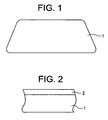
- a coated structure according to an exemplary embodiment of the invention is shown in Figure 2 .
- the coated structure includes a substrate 1 and a UV absorption layer 2.
- the thickness of the substrate 1 and UV absorption layer 2 is not necessarily to scale.
- the substrate 1 comprises a clear polymeric material such as polycarbonate.
- the UV absorption layer 2 is indium doped zinc oxide (IZO).
- the coated substrate is preferably a vehicle window, such as a car, truck, motorcycle, tractor, boat or airplane window, as shown in Figure 1 .
- the coated substrate may be used in other applications, such as building windows, architectural materials, or manufacturing apparatus portholes, e.g. viewing areas that allow the user to look inside metal or industrial manufacturing apparatus.
- the substrate may also comprise a display screen, such as a television screen, an LCD screen, a computer monitor screen, a plasma display screen or a glare guard for a computer monitor. Display screens benefit from being coated with the UV absorption layer to prevent the screen from turning yellow and to prevent UV radiation from damaging electronic components inside the display.
- the substrate 1, comprises a polymer resin.
- the substrate may comprise a polycarbonate.
- Polycarbonates suitable for forming the substrate are well-known in the art and generally comprise repeating units of the formula: where R is a divalent aromatic radical of a dihydric phenol (e.g., a radical of 2,2-bis(4-hydroxyphenyl)-propane, also known as bisphenol A) employed in the polymer producing reaction; or an organic polycarboxylic acid (e.g. terephthalic acid, isophthalic acid, hexahydrophthalic acid, adipic acid, sebacic acid, dodecanedioic acid, and the like).
- R is a divalent aromatic radical of a dihydric phenol (e.g., a radical of 2,2-bis(4-hydroxyphenyl)-propane, also known as bisphenol A) employed in the polymer producing reaction; or an organic polycarboxylic acid (e.g. terephthalic acid, isophthalic
- polycarbonate resins are aromatic carbonate polymers which may be prepared by reacting one or more dihydric phenols with a carbonate precursor such as phosgene, a haloformate or a carbonate ester.
- a carbonate precursor such as phosgene, a haloformate or a carbonate ester.
- a polycarbonate which can be used is TEXAN®, manufactured by the General Electric Company.
- Aromatic carbonate polymers may be prepared by methods well known in the art as described, for example, in U.S. Patent Nos. 3,161,615 ; 3,220,973 ; 3,312,659 ; 3,312,660 ; 3,313,777 ; 3,666,614 ; 3,989,672 ; 4,200,681 ; 4,842,941 ; and 4,210,699 .
- the substrate may also comprise a polyestercarbonate which can be prepared by reacting a carbonate precursor, a dihydric phenol, and a dicarboxylic acid or ester forming derivative thereof.
- Polyestercarbonates are described, for example, in U.S. Patent Nos. 4,454,275 ; 5,510,448 ; 4,194,038 ; and 5,463,013 .
- polyestercarbonate PPC
- PES polyethersulfone
- Radel® by Amoco
- PEI polyetherimide
- Ultem® by the General Electric Company
- the substrate can be formed in a conventional manner, for example by injection molding, extrusion, cold forming, vacuum forming, blow molding, compression molding, transfer molding, thermal forming, and the like.
- the article may be in any shape and need not be a finished article of commerce, that is, it may be sheet material or film which would be cut or sized or mechanically shaped into a finished article.
- the substrate may be rigid or flexible.
- the substrate may be transparent or not transparent.
- the UV absorption layer 2 typically comprises a doped metal oxide having a thickness of 1-1000 nm, typically 300-600 nm.
- IZO indium doped zinc oxide
- the IZO layer displays superior UV absorption and weather resistance as compared to other UV absorption materials.
- the IZO layer shows excellent weather resistance since it does not become hazy or lose its ability to absorb UV light after being submerged for an extended period in 65° C water.
- IZO layers had an optical density of at least 4 at 350 nm showing substantially no Increase in haze, and only a negligible decrease in UV absorption.
- Optical density (“OD”, also referred to as "absorbance”) is defined as log(I i /I q ), where I i is the intensity of incident light on the doped zinc oxide layer and I o is the output intensity. Unless otherwise specified the wavelength of light at which optical density is measured is 350 nm (UV).
- the IZO film exhibits excellent absorbance In the UV region (wavelengths of 1 to 380 nm), it protects polymeric substrates from turning yellow, unlike coatings that contain prior art UV absorbers.
- the IZO layers of the present invention have optical density values greater than than 2.0, typically greater than 3.0, more typically greater than 4.0, at 350 nm.
- the IZO layer maintains chemical stability and desirable optical properties even with a relatively high indium content.
- Indium comprises 2-15 atomic percent of the total metal content of the IZO layer 2, such that the material has the following atomic composition: in 0.02-0.15 Zn 0.85-0.88 O, while maintaining good chemical stability and UV absorption.
- the indium content may comprise greater than 3.0, 5.0, or 10.0 atomic percent of the total metal content of the IZO layer.
- IZO layers having a relatively high initial optical density, e.g. 3.0, a low loss of optical density under a water soak test, e.g. 0.02 per day, and a relatively low increase in haze under the water soak test, e.g. 0.3% per day.
- DC magnetron sputtering produces IZO layers having a relatively high initial optical density, e.g. 3.0, a low loss of optical density under a water soak test, e.g. 0.02 per day, and a relatively low increase in haze under the water soak test, e.g. 0.3% per day.
- IZO also provides the advantage that the IZO layer is electrically conductive. Therefore the IZO layer of the present invention may be used as a window defogger on an automobile window, since it is typically transparent. Another application of IZO layer(s) of the present invention may be in theft or break-in deterrence.
- a window coated with the IZO layers may carry a low current passed through the IZO layers. When a window is broken by a thief or chemically attacked, the current flow through the IZO layers is interrupted which sets off an alarm.
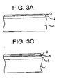
- FIG. 3A An alternative embodiment of the present invention is shown in Figure 3A .
- an optional scratch or abrasion resistant coating 3 is formed on the metal oxide UV absorption layer 2.
- the abrasion resistant layer 3 minimizes or even prevents the UV absorption layer 2 from being scratched during use.
- the abrasion resistant layer 3 may comprise, for example, a plasma polymerized organosilicon material, as described in EP-A-1165856 (GE Docket No. RD-25993), entitled “Multilayer Article and Method of Making by Arc Plasma Deposition", by lacovangelo et al., filed on the same day as the present application.
- the organosilicon material may comprise, for example, octamethylcyclotetrasiloxane (D4) tetramethyldisiloxane (TMDSO), hexamethyldisiloxane (HMDSO), or other organosilicon, as described in the above copending application.
- the organosilicon monomers are oxidized, decomposed, and polymerized In an arc plasma deposition apparatus, typically with a stoichiometric excess oxygen, to form an abrasion resistant layer which comprises an oxidized D4, TMDSO, or HMDSO layer, for example.
- Such an abrasion resistant layer may be referred to as an SiO x layer.
- the SiO x layer may also contain hydrogen and carbon atoms in which case it is generally referred to as SiO x C y H z .
- abrasion-resistant material examples include silicon dioxide and aluminum oxide, for example, or mixtures thereof.
- an interlayer 6 may be formed between the metal oxide UV absorption layer 2 and the abrasion resistant layer 3, as shown in Figure 3C .
- Layer 5 relives stress between layers 2 and 3 that occurs due to different coefficients of thermal expansion, different ductility and different elastic modulus of layers 2 and 3.
- Layer 5 may comprise aluminum or a polymerized organosilicon, for example
- the interlayer 5 is optional, and may be omitted if layer 2 comprises IZO since this layer acts as a compliant layer for an outer abrasion resistant layer due to its Intermediate coefficient of thermal expansion, high ductility and modulus.
- one or more of the layers depicted in Figures 3A and 3C may be applied to both sides of the substrate 1.
- both the outside and inside surfaces of the substrate may include an interlayer 4, a UV absorption layer 2, and an abrasion resistant layer 3.
- the outside surface of the substrate may include one or more of layers 2, 3, 4, 5, 6, while the inside surface of the substrate 1 includes one or more of layers 2, 3, 4, 5, 6.
- the metal oxide UV absorption layer may be deposited by a variety of methods, such as chemical vapor deposition (CVD), evaporation (thermal, RF of electron beam), reactive evaporation, suttering (DC, RF, microwave and/or magnetron), arc plasma deposition, and reactive sputtering.
- CVD chemical vapor deposition
- evaporation thermal, RF of electron beam
- reactive evaporation suttering
- DC RF, microwave and/or magnetron
- arc plasma deposition arc plasma deposition
- reactive sputtering Typically, the layers are deposited by RF and DC magnetron sputtering.
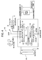
- FIG. 4 illustrates an apparatus which may be used to deposit the layers of the coated article by reactive sputtering, according to an exemplary embodiment of the invention.
- the reactive sputtering apparatus 60 preferably comprises a reactant target 61, a substrate holder or support 62, a plasma reaction space 63 between the support and the target, an optional shutter 64 that separates the target from the support, a plasma gas supply tank 65, a reactant gas supply tank 66 for reactive sputtering, and DC or RF voltage supple lines 67 and 67'.
- the apparatus may optionally comprise a testing probe/oscilloscope 68.
- the apparatus is preferably evacuated by at least one mechanical pump, turbo pump, and/or cryopump 69.
- the target 61 may be cooled by flowing water on its back side.
- the support 62 may be heated, cooled or biased as desired.
- magnets 70 may be provided above or adjacent to the target 61 to form a DC or RF magnetron sputtering apparatus.
- the target 61 preferably comprises solid IZO containing 0-15 weight %, and preferably 1.5 weight % indium, and the sputtering gas comprises Ar or a mixture of Ar with an oxidant such as oxygen or nitrous oxide (N 2 O).
- the target may comprise In:Zn of the same indium content as the IZO target and the sputtering gas may comprise a mixture of Ar and oxygen or N 2 O (i.e. the IZO layers may be formed by reactive sputtering).
- the chamber 63 is typically pumped down by pump(s) 69.
- a sputtering gas such as Ar
- Ar is filled into space 63 from gas supply tank 65.
- a DC or RF voltage is applied to the target, which causes the sputtering gas to form a plasma.
- the plasma atoms and ions bombard the target due to the negative charge applied to the target.
- the plasma bombardment causes reactant atoms to be sputtered off from the target 61 and to drift toward the substrate 1 on the support 62.
- adjacent but separate Zn and In targets may be used to form the IZO layer.
- the Ar plasma may be used to bombard the substrate 1. This causes the plasma to sputter clean the substrate 1 or any layers thereon prior to depositing layer 2. This increases process throughput by eliminating a separate cleaning step in a separate chamber.
- an abrasion resistant and/or adhesion layer may be deposited in the same sputtering chamber.
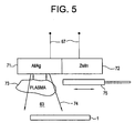
- the target may comprise an Ag or At portion 71 and a In:Zn or an IZO portion 72.
- DC or RF voltage is then applied to target portion 71, while portion 72 may be covered with a shutter 75.
- portion 72 is simply covered by shutter 75.
- the plasma 73 only bombards the uncovered target portion 71, causing only Ag or Al atoms 74 to be sputtered toward the substrate 1.
- the Ag or Al film is sputter deposited on substrate 1.
- the substrate 1 may be similarly cleaned before depositing layer 6. However, the cleaning step may be omitted.
- portion 71 is then applied only to target portion 72, while portion 71 may be covered with a shutter 75.
- portion 71 is simply covered by shutter 75.
- the plasma 73 bombards only target portion 72 to sputter off Zn, In and oxygen atoms to form an IZO layer on or over the adhesion layer 6. Forming the various layers and carrying out sputter cleaning in the same chamber greatly enhances process speed and throughput.
- the abrasion resistant layer or other layer may also be formed in the same apparatus as the UV absorbing layers.
- an extra sputtering target may be added to the chamber.
- the target may comprise silicon for reactive sputtering or silicon dioxide for inert gas sputtering to form a silicon dioxide layer.
- extra targets are preferably covered by shutter 75 when other layers are being sputtered.
- the doped metal oxide coating according to exemplary embodiments of the invention exhibits excellent weathering and protects polymeric substrates from turning yellow
- a method of protecting polymeric substrates from UV degradation comprising coating the polymeric substrate with a layer comprising a doped metal oxide such as IZO.
- the method may also include deposition of an abrasion resistant layer and a stress relieving interlayer.
- the various layers may be applied by methods other than sputtering, such as arc plasma deposition.
- An arc plasma deposition apparatus for depositing the UV absorption layers according to another embodiment of the invention is shown in Figure 6 .
- the apparatus comprises a plasma generation chamber 10 and a deposition chamber 11.
- the deposition chamber 11 contains a substrate 20 mounted on a temperature controlled support 22.
- the substrate 20 may be a transparent polymeric substrate 1 shown in Figure 1 .
- the support 22 may be positioned at any position within the interior 21 of chamber 11. Typically, the substrate 20 is positioned about 15-35 cm, most typically 25,5 cm, from the anode of the plasma generation chamber 10.
- Chamber 11 also optionally comprises a retractable shutter 24.
- the shutter may be positioned by any suitable means, such as by a handle 25 or by a computer controlled positioning mechanism.
- the shutter 24 may also contain a circular aperture to control the diameter of the plasma that emanates from the plasma generation chamber 10 towards the substrate 20.
- Chamber 11 may also optionally comprise magnets or magnetic field generating coils (not shown) adjacent to chamber walls to direct the flow of the plasma.
- Chamber 11 may also contain an optional nozzle 18.
- the nozzle 18 provides Improved control of the injection, ionization and reaction of the reactants to be deposited on the substrate 20.
- the nozzle 18 assists in assuring the deposition of a solid metal oxide film or layer on the substrate 20 and reduces or even prevents formation of powdery reactant deposits on the substrate 20.
- the nozzle 18 has a conical shape with a divergent angle (measured from one inner surface to the opposite inner surface) of about 25-60 degrees, most typically 40 degrees, and a length of about 16 cm.
- the nozzle 18 may have a variable cross section, such as such as conical-cylindrical-conical or conical cylindrical, a divergent angle other than 40 degrees and a length other than 16 cm.
- the nozzle may also be omitted entirely.
- Chamber 11 also contains at least one reactant supply line.
- chamber 11 may contain an oxygen supply line 12, a zinc supply line 14, and an indium line 16 to deposit IZO or AZO on the substrate 20.
- the supply lines 12, 14 and 16 preferably communicate with the nozzle 18 and supply reactants into the plasma flowing through the nozzle.
- Chamber 11 also contains vacuum pumps (not shown) for evacuating the chamber.
- the plasma generation chamber 10 contains at least one cathode 13, a plasma gas supply line 17 and an anode 19.
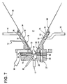
- One embodiment of the plasma generation chamber 10 is shown in more detail in Figure 7 .
- Each cathode 13 may comprise tungsten or thorium doped tungsten tips. The use of thorium allows the temperature of the tips to be maintained below the melting point of tungsten, thus avoiding contamination of the plasma with tungsten atoms.
- Each cathode 13 may be surrounded by a cathode housing 83 to isolate each cathode 13 from the walls of the cathode support plate 28.
- the cathode housing 83 may suitably comprise a shell surrounding an isolating mantle made from an insulating material such as quartz.
- the anode 19 typically has a central aperture in the form of a diverging cone.
- Each cathode 13 is typically separated from the anode 19 by at least one cascade plate 26.
- the cascade plate(s) preferably comprise copper discs containing a central aperture corresponding to the shape of the aperture in the anode 19.
- the plasma generation chamber 10 also contains at least one plasma gas supply line 17.
- chamber 10 may also contain a purging gas supply line adjacent to the plasma gas supply line 17 to supply a purging gas to chambers 10 and 11 prior to supplying a plasma gas.
- the cathode support plate 28 may be attached to the cascade plate(s) 26 and the anode 19 by an insulated bolt 27 or by other fasteners.
- the cascade plate 26 is typically electrically Insulated from the cathode support plate 28 and the anode 19 by spacers 15.
- Spacers 15 may comprise any suitable material, for example O-ring vacuum seals, polyvinylchloride rings and/or boron nitride rings.
- the cascade plate(s) 26 and the anode 19 include cooling channels 29 and 99, respectively.
- the channels 29 and 99 have a circular shape within the interior volume of the plate(s) 26 and the anode 19. Chilled water supplied through a water supply line 89 flows through the channel 99 to cool the anode 19 during operation.
- a similar water supply line (not shown) supplies water to the channel 29 to cool the cascade plate(s) 26.
- the nozzle 18 is preferably attached to the anode 19.
- the nozzle 18 may contain an integral or removable divergent portion 88 for directing the plasma and reactive species flow.
- the reactant supply line(s) 12, 14 and 16 are in communication with the nozzle 18.
- the nozzle 18 may contain a showerhead nozzle supply line which comprises a ring shaped reactant supply channel(s) connected to injection holes.
- reactant supply line 14 connects to reactant supply channel 35 formed Inside the body of the nozzle 18.
- Reactant supply channel 35 contains a plurality of openings 34, which are preferably evenly distributed around the circumference of channel 35. The reactant flows from line 14 into the channel 35.
- the reactant then flows from the channel 35 simultaneously through openings 34 to enter the plasma, emanating from anode 19 into deposition chamber space 21, from several directions.
- supply line 16 is connected to channel 33 and openings 32 and supply line 12 is connected to channel 31 and openings 30.
- the channel and openings may be omitted and the supply lines may deposit the reactants directly into the plasma, if desired.
- a plasma gas is supplied through plasma gas supply line 17.
- the plasma gas may comprise any suitable gas, such as any noble gas, nitrogen, ammonia, nitrous oxide, carbon dioxide or hydrogen or any mixture thereof. It there is more than one plasma gas, then the plural gasses may be supplied through plural supply lines.
- the plasma gas comprises argon or a combination of argon and oxygen.
- the plasma gas in plasma generation chamber 10 is maintained at a higher pressure than the pressure in the deposition chamber 11, which Is continuously evacuated by a pump.
- An arc voltage is then applied between the cathode(s) 13 and the anode 19 to generate a plasma in the chamber 10.
- the plasma then shoots out as a supersonic plasma through the anode 19 aperture Into the deposition chamber 11 due to the pressure difference between chambers 10 and 11.
- the reactants are supplied into the plasma through the supply lines 12, 14, 16.
- oxygen gas may be supplied through line 12
- zinc may be supplied through line 14
- indium or aluminum may be supplied through line 16 to form an IZO film on substrate 20.
- Zinc and indium or aluminum may be supplied through the same line (14 or 16).
- the supply line location may be altered, and oxygen may be supplied through line 14 or 16, etc.
- Zinc and indium reactants may be supplied though a supply line in the form of metal organic gases, such as diethyl zinc, dimethyl zinc, triethyl indium or trimethyl indium, which disassociate in the plasma stream.
- metal organic gases such as diethyl zinc, dimethyl zinc, triethyl indium or trimethyl indium, which disassociate in the plasma stream.
- the zinc and/or indium reactants are supplied in the form of a metal vapor.
- the metal supply line may be altered, for example as shown in Figure 8 .
- the metal supply line 14 (or 12 or 16, as necessary) may be replaced by a tube 44, such as a stainless steel tube.
- the tube 44 Is attached to a crucible 45, such as a nickel crucible with a tantalum liner.
- the crucible is surrounded by a heating element 47, such as a high resistance wire or RF coils.
- the heating element is also wrapped around the tube 44.
- the heating element is kept at a temperature sufficient to prevent the metal from solidifying in the tube 44.
- the heating element is kept above the melting point of zinc, and typically above 800° C.
- the heating element 47 also extends to the nozzle 18 to prevent the metal from solidifying therein.
- the metal reactant 48 is preferably loaded into the crucible 47 such that the reactant abuts the pipe 44.
- the heating element Is activated to evaporate the metal reactant 48 into the pipe 44.
- the metal reactant is then fed into the plasma 50 from pipe 44 through channel 35 and openings 34.
- the metal reactant is zinc.
- the metal reactant 48 may be an in:Zn alloy, such as 2.5 atomic % in:Zn.
- indium vapor may be supplied through a conduit separate from the zinc vapor conduit.
- the second metal supply line 16 is replaced with a second tube 46 and a second crucible containing Indium.
- the zinc and indium vapor enter the plasma, where they mix with oxygen supplied through supply line 12.
- the metals and oxygen reactants mix in the plasma 50 to form IZO which deposits on the substrate 20 as a thin film as the plasma strikes the substrate.
- At least one reactant inlet such as a metal reactant inlet 54
- the inlet 54 may have a ring shape with a wide aperture in the center of the ring.
- the inlet preferably contains a reactant supply channel 35 and reactant supply openings 34 similar to the previous embodiment, such as the ones shown in Figure 8 .
- the plasma 50 passes through the aperture in the Inlet 54.
- the reactant is supplied to channel 35 through a supply line 14 if the reactant is a gas or through a pipe 44 and crucible 45 if the reactant is a vapor.
- the reactant 48 enters the plasma 50 from plural openings 34.
- the nozzle 18 may be omitted because the Inlet 54 controls the shape and direction of the plasma 50.
- the reactant inlet may comprise a crucible 55, as shown for example in Figure 10 .
- Solid Zn; In:Zn, or Al:Zn 48 may be evaporated from the crucible 55 directly into the plasma 50.
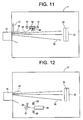
- the reactant source may comprise a biased sputtering target 56 (e.g. cathode) adjacent to a biased anode 57, as shown for example in Figure 11 .
- Edge portions of the plasma 80 are drawn to the biased target 56 and sputter off target atoms 48, that drift into the main portion of the plasma 50.
- the reactant atoms combine in the plasma and are deposited on the substrate 20 by the arc.
- the target 56 may comprise any suitable material, such as Zn, In:Zn, ZnO or IZO. If the target 56 contains oxygen, then a separate source of oxygen may be omitted. Likewise, the injection nozzle 18 may be omitted.
- the reactant source comprises an e-beam evaporation system, as shown for example in Figure 12 .
- An electron gun 58 emits a beam of electrons 60.
- the electron beam is directed toward a reactant target 61 by magnet(s) 59.
- the reactant target is a rotating wheel to allow uniform reactant release from the target 61.
- the reactant atoms 48 migrate toward the plasma 50 to be deposited on the substrate 20.
- the target 61 may comprise Zn, In:Zn, ZnO or IZO. If the target 61 contains oxygen, then a separate source of oxygen may be omitted. Likewise, the nozzle 18 may be omitted.
- the abrasion resistant layer 3, the interlayer(s) 4 and/or 5 and the adhesion promoting layer 6, if any are utilized in the structure may be formed In the same chamber as the UV absorbing layers.
- a silicon dioxide, alumina, or polymerized organosilicon abrasion resistant coating may be deposited by supplying oxygen and silicon or aluminum or organosilicon reactants into the plasma.
- a purging gas is flown through chamber 11 between depositions of each layer. Deposition of several layers in the same chamber increases process throughput and decreases process cost.
- optical density refers to the absorbance of radiation having a wavelength of 350 nanometers (UV), defined as log(I i ,I o ), where I i is the intensity incident on the deposit and I o is the output intensity.
- UV nanometers
- Optical density was measured on a Unicam UV-3 spectrometer. Haze refers to the percentage of light scattering. The haze was measured using a Gardner XL-835 colorimeter. In Table 1 below, “high power” is 100 W (4.9 W/cm 2 ), and “low power” is 75 W (3.68 W/cm 2 ).
- Examples 1-2 the samples were subjected to a water soak test involving submerging the sample in 65° C water for 24 hours.
- Examples 3-9 were subjected to a QUV® accelerated weathering test (hereinafter the "QUV test").
- QUV test QUV® accelerated weathering test
- This test was carried out in a model QUV environmental chamber manufactured by the Q-Panel Company. Samples were placed In the chamber and exposed for consecutive cycles, each cycle consisting of 5 hours at 60°C with exposure to UV light (295 nm-370 nm, with a maximum at 340 nm, using UVA-340 lamps) followed by 1 hour at 50°C with moisture condensation.
- a glass substrate was cleaned in isopropyl alcohol and air dried.
- the reactor chamber was pumped to 2.7 x 10 -4 Pa prior to introduction of the reactive gas.
- the substrate was sputter etched at 100 watts for 2 minutes in an argon plasma at 1.2 Pa.
- the thickness of the ZnO layer was about 500 nm.
- the ZnO layer was subjected to a water soak test by being submerged in 65°C water for 24 hours.
- the optical density at a wavelength of 350 nm and the haze were measured before and after the water soak test.
- the optical density of the ZnO layer decreased from 4.0 to 3.2, and ⁇ %H was 7% after the water soak test.
- Example 1 The experiment of example 1 was repeated, except that the Ar sputtering gas was replaced with an Ar and 10% O 2 sputtering gas.
- the QUV test was conducted, as described above, for 300 hours. The OD decreased from 4.2 to 3.4 after the QUV test. ⁇ %H was 1.4%.
- Example 3 The experiment of example 3 was repeated, except that the ZnO layer was replaced with an In 0.025 Zn 0.975 O layer deposited by DC magnetron sputtering from a 1.5 weight % indium IZO target and the sputtering power was decreased to 75 W.
- the OD remained constant at 4.2 after 300 hours of the QUV test. ⁇ %H after the QUV test was 0%.
- Table 1 The results of the weathering tests are summarized in Table 1 below.
- Table 1 # Coating Plasma Power Hours OD Results After Weathering Test OD ⁇ %H 1 ZnO Ar High 24 4.0 3.2 7 2 ZnO 7% O 2 High 24 3.9 3.5 5 3 ZnO 10%O 2 High 300 4.2 3.4 1.4 4 ZnO 10%O 2 High 1000 4.2 3.4 10 5 IZO Ar Low 300 4.2 4.2 0.0 6 IZO Ar High 300 4.0 4.0 0.0 7 IZO Ar Low 1000 4.2 4.0 0.0 8 IZO Ar High 1000 4.2 4.0 0.0 9 ZnO/SiO 2 10%O 2 High 1000 4.2 4.1 12
- Examples 1 and 2 which were ZnO deposited with Ar and 7% O 2 /Ar plasma, turned hazy after only 1 day of the water soak test.
- examples 3-4 deposited with 10% oxygen exhibited good stability with little change after 300 hours of the QUV test.
- the OD also deteriorated from 4.2 to 3.4. Therefore, ZnO layers with acceptable weather resistance may be deposited by reactive sputtering when sufficient oxygen reactant is present In the plasma.
- IZO samples 5-8 showed no significant degradation after 300 or 1000 hours of the QUV test, either in OD or haze.
- Samples 5 and 7 were deposited at a lower power (75 W) which results in a higher stress in the deposit. Based on this data there does not appear to be an effect of stress on stability.
- the preferred metal oxide UV absorbing layer 2 of the coated structure described above has an optical density of at least 4.0 and exhibits substantially zero increase in haze after being exposed the QUV test for 300 or 1000 hours.
- a ZnO layer was deposited on glass by RF magnetron sputtering in an argon/10% oxygen plasma at a power of 100 W.
- the sample had an initial optical density of 4.2.
- the sample was then subjected a UV accelerated weathering test in an Atlas Ci35a xenon arc Weatherometer® using Type S borosilicate inner and outer filters.
- the irradiance level was 0.77 W/m 2 at 340 nm.
- the black panel temperature was 70-73° C.
- the dry bulb temperature was 45° C with a wet-bulb depression of 10° C (50% RH).
- the cycle was 160 minutes light, 5 minutes dark, 15 minutes dark with water spray. This cycle accumulates 2.46 kJ/m 2 at 340 nm per hour of run-time.
- the following examples 11-18 illustrate additional methods of forming a doped zinc oxide layer with improved weatherability.
- the weatherability data i.e. increase in haze and loss of UV absorbency, are presented in Table 2 below.
- the samples were subjected to a water soak test, in which the samples were submerged in 65° C water for the time periods specified below.
- a layer of ZnO was deposited by RF magnetron sputtering at a power of 100 W with a ZnO target.
- the initial optical density was 2.5.
- the average increase in haze during a 7-day water soak test was 4.0% per day.
- the average daily loss of optical density was 0.45.
- a layer of IZO containing indium in the amount of 2.5 atomic percent of the total metal content of the IZO layer was deposited by RF sputtering.
- the target was IZO with indium comprising 2.5 atomic percent of the total metal content of the target.
- the initial optical density was 2.4.
- the average daily increase in haze during the 10-day water soak test was 3.0%.
- the average daily loss of optical density was 0.25.
- a layer of IZO containing indium in the amount of 5.0 atomic percent of the total metal content of the IZO layer was deposited by RF magnetron sputtering.
- the target was IZO with indium comprising 5.0 atomic percent of the total metal content of the target.
- the initial optical density was 1.5.
- the average daily increase in haze during the 21-day water soak test was 4.0%.
- the average daily loss of optical density was 0.05.
- a layer of IZO containing indium in the amount of 2.5 atomic percent of the total metal content of the IZO layer was deposited by DC magnetron sputtering.
- the target was IZO with indium comprising 2.5 atomic percent of the total metal content of the target.
- the initial optical density was 3.0.
- the average daily increase in haze during the 21-day water soak test was 0.3%.
- the average daily loss of optical density was 0.02.
- a layer of IZO containing indium in the amount of 10.0 atomic percent of the total metal content of the IZO layer was deposited by RF sputtering.
- the target was IZO with indium comprising 10.0 atomic percent of the total metal content of the target.
- the initial optical density was 2.9.
- the average daily increase in haze during the 23-day water soak test was 0.6%.
- the average daily loss of optical density was 0.12.
- a layer of IZO containing indium in the amount of 15 atomic percent of the total metal content of the IZO layer was deposited by RF sputtering.
- the target was IZO with indium comprising 15 atomic percent of the total metal content of the target.
- the initial optical density was 2.2.
- the average daily increase in haze during the 23-day water soak test was 0.4%.
- the average daily loss of optical density was 0.08.
- a layer of AZO containing aluminum in the amount of 2.5 atomic percent of the total metal content of the AZO layer was deposited by DC magnetron sputtering.
- the target was aluminum doped zinc oxide with aluminum comprising 2.5 atomic percent of the total metal content of the target.
- the initial optical density was 3.0.
- the average daily increase in haze during the 21-day water soak test was 3.0%, The average daily loss of optical density was 0.04.
- a layer of AZO containing aluminum in the amount of 2.5 atomic percent of the total metal content of the AZO layer was deposited by RF magnetron sputtering.
- the target was aluminum doped zinc oxide with aluminum comprising 2.5 atomic percent of the total metal content of the target.
- the initial optical density was 4.0.
- the average daily increase in haze during the 21-day water soak test was 2.0%.
- the average daily loss of optical density was 0.05. Table 2 Ex.
- the IZO layer of example 14 prepared by DC magnetron sputtering had a relatively high initial optical density of 3.0, a low daily decrease in optical density (0.02), and a low daily increase in haze (0.3). These properties were achieved with an indium content of 2.5%. Examples 15 and 16 also exhibited a relatively low decrease in optical density and increase in haze, but the indium content was considerably higher, i.e. 10% and 15%, respectively.
- the AZO layers of examples 17 and 18 exhibited a relatively high initial optical density and a relatively low loss in optical density per day. However, the increase in haze of the AZO layers was relatively high at 3.0% and 2.0% per day.
- a preferred doped zinc oxide UV absorbing layer is formed by DC magnetron sputtering and has an initial optical density of at least 3.0, and after a water soak test for 21 days has a daily decrease in optical density of at most 0.02 and a daily increase in haze of at most 0.3.
- Other preferred doped zinc oxide coatings have initial optical densities of at least 2.0, and after water soak testing for 23 days, have a daily decrease in optical density of at most 0.12 and a daily increase in haze of at most 0.6.
- An IZO sample was deposited on glass by DC magnetron sputtering in an argon plasma at a power of 100 W.
- the IZO layer contained indium in the amount of 2.5 atomic percent of the total metal content of the IZO layer.
- the target was IZO with indium comprising 2.5 atomic percent of the total metal content of the target.
- the initial optical density of the sample was 3.09.
- Example 10 The sample was then subjected to a UV accelerated weathering test in a xenon arc weatherometer, as described above in Example 10. After 3786 hours in the weatherometer (8945 KJ/m 2 ), the optical density had decreased only slightly to 2.93. There was no increase in haze as compared to a control sample comprising glass.
- An IZO sample was deposited on glass by sputtering DC magnetron in an argon plasma at a power of 100 W.
- the IZO layer contained indium in the amount of 2.5 atomic percent of the total metal content of the IZO layer.
- the target was IZO with indium comprising 2.5 atomic percent of the total metal content of the target.
- the initial optical density of the sample was 3.52.
- Example 10 The sample was then subjected to a UV accelerated weathering test in a xenon arc weatherometer, as described above in Example 10. After 3786 hours in the weatherometer (8945 KJ/m 2 ), the optical density had decreased only slightly to 3.43. There was no increase in haze as compared to a control sample comprising glass.
- Examples 19-20 illustrate that a UV absorbing layer formed of indium doped zinc oxide can have a relatively high optical density and can maintain that optical density for a substantial period of time under accelerated weathering conditions.
- arc plasma deposition as described above with respect to Figures 6-8 , was used to deposit doped zinc oxide layers on glass.
- the arc plasma generator Included a copper anode separated from three needle-type cathodes of thoriated tungsten by at least one electrically isolated copper disk.
- Each chamber was pumped to less than 1 milliTorr and back flushed with nitrogen to about 500 Torr then pumped back down at least two times to remove residual moisture from the chamber prior to introduction of the reactants.
- the substrates were etched at 50 W for 10 seconds In an argon plasma (2 lpm Ar) at 20-30 mT.
- the working distance (anode to substrate) for all examples was 25.5 cm.
- Zn Srce refers to the zinc source, which is either dimethyl zinc (DMZ) or solid zinc (Zn) evaporated In a crucible.
- Dopant Srce refers to the source of the dopant, trimethyl aluminum (TMA) or triethyl indium (TEI).
- % Dopant refers to the amount of dopant in the layer in terms atomic percent of the total metal content of the layer.
- An aluminum doped zinc oxide layer was deposited on glass.
- the zinc source was dimethyl zinc.
- the aluminum source was trimethyl aluminum.
- the dimethyl zinc flow rate was 0.6 lpm.
- the TMA flow rate was 0.06 lpm.
- the oxygen flow rate was 6.7 lpm.
- the argon flow rate was 1.25 lpm.
- the arc current was 60 amps.
- the pressure was 100 mT.
- the AZO layer had a thickness of 0.52 microns and was deposited in 5 seconds.
- the optical density of the AZO layer at 350 nanometers was 2.48.
- An aluminum doped zinc oxide layer was deposited on glass.
- the zinc source was solid zinc which was evaporated into the plasma.
- the aluminum source was trimethyl aluminum.
- the zinc temperature was 800° C.
- the TMA flow rate was 0.06 lpm.
- the oxygen flow rate was 4.0 lpm.
- the argon flow rate was 1.5 lpm.
- the arc current was 35 amps.
- the pressure was 80 mT.
- the AZO layer had a thickness of 0.38 microns and was deposited in 20 seconds.
- the optical density of the AZO layer at 350 nanometers was 1.95.
- An indium doped zinc oxide layer was deposited on glass.
- the zinc source was solid zinc which was evaporated into the plasma.
- the indium source was triethyl indium.
- the zinc temperature was 800° C.
- the TEI flow rate was 0.06 lpm.
- the oxygen flow rate was 4.0 lpm.
- the argon flow rate was 1.5 lpm.
- the arc current was 35 amps.
- the pressure was 80 mT.
- the IZO layer had a thickness of 0.63 microns and was deposited in 20 seconds.
- the optical density of the AZO layer at 350 nanometers was 3.8. Table 3 # Layer Zn Srce Dopant Srce % Dopant OD 21 AZO DMZ TMA 2.5 2.48 22 AZO Zn TMA 2.5 1.95 23 IZO Zn TEI 2.8 3.8
Abstract
Description
- The present invention relates generally to a coating for transparent substrates with high UV absorbency and excellent weatherability, and more particularly to a doped metal oxide coating for transparent polymeric substrates.
- Car manufacturers have traditionally used glass as the material for car windows. However, recently it has become desirable to substitute glass windows with polymeric windows, such as polycarbonate (PC) windows. Polymeric windows are often advantageous compared to glass windows because of their low weight, high strength and ease of shaping. However, some polymeric windows, such as PC windows, turn yellow after being exposed to the ultraviolet (UV) radiation in sunlight. The yellow windows suffer from poor transmission of visible light, thus making them unsuitable for many car window applications.
- One solution to the UV damage problem is to coat the polymeric substrates with a TiO2 (titanium dioxide) layer. The TiO2 coating acts as a partial absorber of UV radiation and provides a measure of protection for some applications. However, TiO2 generally provides an insufficient amount of UV absorption, and windows coated with TiO2 eventually turn a shade of yellow. TiO2 is also a photocatalyst for oxidation of polymers. Therefore. TiO2 coated polymers are generally unsuitable as a car window material.
- Another solution to the UV damage problem is to coat the polymers with a ZnO (zinc oxide) layer. Zinc oxide provides UV absorption to higher wavelengths than TiO2, providing greater protection for polycarbonate and other polymeric substrates. Therefore, polymers coated with ZnO generally do not turn yellow when exposed to sunlight. However, prior art ZnO coatings are known to dissolve in water. Poor water soak stability on many substrates, including polycarbonate (PC), has thus surfaced as one potential limitation to the use of ZnO as a UV absorber for car windows, because car windows are frequently exposed to rain and snow.
-
U.S. Patent No. 5,008,148 is directed to a process for coating molded plastic articles of thermoplastic polycarbonates or thermoplastic polyarylene sulfides with metal oxides. The molded articles are coated with metal oxides which absorb electromagnetic radiation at wavelengths from 250 nm to 400nm. In view of the foregoing, it would be beneficial to have a coating for a transparent substrate that exhibits good UV absorption and chemical stability. It would also be desirable to have a method for effectively applying such a coating. - According to an exemplary embodiment, the invention provides a method of preparing a layered structure which includes a polymeric substrate and a weather-resistant and UV absorbent doped zinc oxide layer on the polymeric substrate. The doped zinc oxide layer is indium doped zinc oxide (IZO).
- The invention also relates to a method of forming an indium doped zinc oxide layer on a substrate comprising the steps of placing the substrate in a sputtering chamber, providing indium and zinc in at least one target, and performing DC magnetron sputtering on the target to form an indium doped zinc oxide layer on the substrate.
-
-
Figure 1 shows an example of a substrate according to one embodiment of the invention. -
Figure 2 is side cross sectional view of a glazed substrate according to an embodiment of the present invention. -
Figures 3A and 3C are side cross sectional views of a glazed substrate according to alternative embodiments of the present invention. -
Figure 4 is a side cross sectional view of an exemplary apparatus used to manufacture the glazed substrate. -
Figure 5 is a side cross sectional view of an apparatus used to manufacture the glazed substrate according to another embodiment of the present invention. -
Figure 6 is a side cross sectional view of an apparatus used to manufacture the glazed substrate according another embodiment of the invention. -
Figure 7 is a side cross sectional view of a portion of the apparatus shown inFigure 6 . -
Figures 8-12 are side cross sectional views of exemplary apparatus used to manufacture the glazed substrate according to other embodiments of the invention. - A coated structure according to an exemplary embodiment of the invention is shown in
Figure 2 . The coated structure includes asubstrate 1 and aUV absorption layer 2. The thickness of thesubstrate 1 andUV absorption layer 2 is not necessarily to scale. Typically, thesubstrate 1 comprises a clear polymeric material such as polycarbonate. TheUV absorption layer 2 is indium doped zinc oxide (IZO). - The coated substrate is preferably a vehicle window, such as a car, truck, motorcycle, tractor, boat or airplane window, as shown in
Figure 1 . The coated substrate may be used in other applications, such as building windows, architectural materials, or manufacturing apparatus portholes, e.g. viewing areas that allow the user to look inside metal or industrial manufacturing apparatus. The substrate may also comprise a display screen, such as a television screen, an LCD screen, a computer monitor screen, a plasma display screen or a glare guard for a computer monitor. Display screens benefit from being coated with the UV absorption layer to prevent the screen from turning yellow and to prevent UV radiation from damaging electronic components inside the display. - The
substrate 1, comprises a polymer resin. For example, the substrate may comprise a polycarbonate. Polycarbonates suitable for forming the substrate are well-known in the art and generally comprise repeating units of the formula:
-
- The substrate may also comprise a polyestercarbonate which can be prepared by reacting a carbonate precursor, a dihydric phenol, and a dicarboxylic acid or ester forming derivative thereof. Polyestercarbonates are described, for example, in
U.S. Patent Nos. 4,454,275 ;5,510,448 ;4,194,038 ; and5,463,013 . - Materials from which the substrate may be formed are polyestercarbonate (PPC), polyethersulfone (PES) (sold under the trademark "Radel®" by Amoco), polyetherimide (PEI or polyimide) (sold under the trademark "Ultem®" by the General Electric Company).
- The substrate can be formed in a conventional manner, for example by injection molding, extrusion, cold forming, vacuum forming, blow molding, compression molding, transfer molding, thermal forming, and the like. The article may be in any shape and need not be a finished article of commerce, that is, it may be sheet material or film which would be cut or sized or mechanically shaped into a finished article. The substrate may be rigid or flexible. The substrate may be transparent or not transparent.
- Referring again to
Figure 2 , theUV absorption layer 2 typically comprises a doped metal oxide having a thickness of 1-1000 nm, typically 300-600 nm. The present Inventor has discovered that the limitations associated with the multilayer films or structures of the prior art can be overcome with a polymeric structure coated with indium doped zinc oxide (IZO). The IZO layer displays superior UV absorption and weather resistance as compared to other UV absorption materials. The IZO layer shows excellent weather resistance since it does not become hazy or lose its ability to absorb UV light after being submerged for an extended period in 65° C water. In addition, after being subjected to a QUV® accelerated weathering test involving exposure to UV radiation, IZO layers had an optical density of at least 4 at 350 nm showing substantially no Increase in haze, and only a negligible decrease in UV absorption. Optical density ("OD", also referred to as "absorbance") is defined as log(Ii/Iq), where Ii is the intensity of incident light on the doped zinc oxide layer and Io is the output intensity. Unless otherwise specified the wavelength of light at which optical density is measured is 350 nm (UV). - Because the IZO film exhibits excellent absorbance In the UV region (wavelengths of 1 to 380 nm), it protects polymeric substrates from turning yellow, unlike coatings that contain prior art UV absorbers. The IZO layers of the present invention have optical density values greater than than 2.0, typically greater than 3.0, more typically greater than 4.0, at 350 nm.
- The present inventor has found that the IZO layer maintains chemical stability and desirable optical properties even with a relatively high indium content. Indium comprises 2-15 atomic percent of the total metal content of the
IZO layer 2, such that the material has the following atomic composition: in0.02-0.15Zn0.85-0.88O, while maintaining good chemical stability and UV absorption. According to various embodiments of the invention, the indium content may comprise greater than 3.0, 5.0, or 10.0 atomic percent of the total metal content of the IZO layer. - The inventor has also discovered that certain deposition methods, e.g. DC magnetron sputtering, produce IZO layers having a relatively high initial optical density, e.g. 3.0, a low loss of optical density under a water soak test, e.g. 0.02 per day, and a relatively low increase in haze under the water soak test, e.g. 0.3% per day. These properties, which indicate good chemical stability, can be achieved by DC magnetron sputtering with a modest amount of indium, e.g. 2-5 atomic percent of the total metal content.
- IZO also provides the advantage that the IZO layer is electrically conductive. Therefore the IZO layer of the present invention may be used as a window defogger on an automobile window, since it is typically transparent. Another application of IZO layer(s) of the present invention may be in theft or break-in deterrence. A window coated with the IZO layers may carry a low current passed through the IZO layers. When a window is broken by a thief or chemically attacked, the current flow through the IZO layers is interrupted which sets off an alarm.
- An alternative embodiment of the present invention is shown in
Figure 3A . In this embodiment, an optional scratch or abrasion resistant coating 3 is formed on the metal oxideUV absorption layer 2. The abrasion resistant layer 3 minimizes or even prevents theUV absorption layer 2 from being scratched during use. The abrasion resistant layer 3 may comprise, for example, a plasma polymerized organosilicon material, as described inEP-A-1165856 (GE Docket No. RD-25993), entitled "Multilayer Article and Method of Making by Arc Plasma Deposition", by lacovangelo et al., filed on the same day as the present application. The organosilicon material may comprise, for example, octamethylcyclotetrasiloxane (D4) tetramethyldisiloxane (TMDSO), hexamethyldisiloxane (HMDSO), or other organosilicon, as described in the above copending application. The organosilicon monomers are oxidized, decomposed, and polymerized In an arc plasma deposition apparatus, typically with a stoichiometric excess oxygen, to form an abrasion resistant layer which comprises an oxidized D4, TMDSO, or HMDSO layer, for example. Such an abrasion resistant layer may be referred to as an SiOx layer. However, the SiOx layer may also contain hydrogen and carbon atoms in which case it is generally referred to as SiOxCyHz. - Other examples of materials suitable for the abrasion-resistant material include silicon dioxide and aluminum oxide, for example, or mixtures thereof.
- In another embodiment of the present invention, an interlayer 6 may be formed between the metal oxide
UV absorption layer 2 and the abrasion resistant layer 3, as shown inFigure 3C . Layer 5 relives stress betweenlayers 2 and 3 that occurs due to different coefficients of thermal expansion, different ductility and different elastic modulus oflayers 2 and 3. Layer 5 may comprise aluminum or a polymerized organosilicon, for example However, the interlayer 5 is optional, and may be omitted iflayer 2 comprises IZO since this layer acts as a compliant layer for an outer abrasion resistant layer due to its Intermediate coefficient of thermal expansion, high ductility and modulus. - According to further embodiments of the invention, one or more of the layers depicted in
Figures 3A and 3C may be applied to both sides of thesubstrate 1. For example, both the outside and inside surfaces of the substrate may include an interlayer 4, aUV absorption layer 2, and an abrasion resistant layer 3. Alternatively, the outside surface of the substrate may include one or more oflayers 2, 3, 4, 5, 6, while the inside surface of thesubstrate 1 includes one or more oflayers 2, 3, 4, 5, 6. - The metal oxide UV absorption layer may be deposited by a variety of methods, such as chemical vapor deposition (CVD), evaporation (thermal, RF of electron beam), reactive evaporation, suttering (DC, RF, microwave and/or magnetron), arc plasma deposition, and reactive sputtering. Typically, the layers are deposited by RF and DC magnetron sputtering.
-
Figure 4 illustrates an apparatus which may be used to deposit the layers of the coated article by reactive sputtering, according to an exemplary embodiment of the invention. Thereactive sputtering apparatus 60 preferably comprises areactant target 61, a substrate holder orsupport 62, aplasma reaction space 63 between the support and the target, anoptional shutter 64 that separates the target from the support, a plasmagas supply tank 65, a reactantgas supply tank 66 for reactive sputtering, and DC or RF voltagesupple lines 67 and 67'. The apparatus may optionally comprise a testing probe/oscilloscope 68. The apparatus is preferably evacuated by at least one mechanical pump, turbo pump, and/orcryopump 69. Thetarget 61 may be cooled by flowing water on its back side. Thesupport 62 may be heated, cooled or biased as desired. In case more precise control of the plasma is desired,magnets 70 may be provided above or adjacent to thetarget 61 to form a DC or RF magnetron sputtering apparatus. - To form IZO layers, the
target 61 preferably comprises solid IZO containing 0-15 weight %, and preferably 1.5 weight % indium, and the sputtering gas comprises Ar or a mixture of Ar with an oxidant such as oxygen or nitrous oxide (N2O). By using a 1.5 weight % indium target, an IZO layer containing 2.5 atomic % indium may be formed. However, the target may comprise In:Zn of the same indium content as the IZO target and the sputtering gas may comprise a mixture of Ar and oxygen or N2O (i.e. the IZO layers may be formed by reactive sputtering). Thechamber 63 is typically pumped down by pump(s) 69. A sputtering gas, such as Ar, is filled intospace 63 fromgas supply tank 65. A DC or RF voltage is applied to the target, which causes the sputtering gas to form a plasma. The plasma atoms and ions bombard the target due to the negative charge applied to the target. The plasma bombardment causes reactant atoms to be sputtered off from thetarget 61 and to drift toward thesubstrate 1 on thesupport 62. Alternatively, adjacent but separate Zn and In targets may be used to form the IZO layer. - Furthermore, by covering the
target 61 withshutter 64 and applying a negative charge to thesupport 62, the Ar plasma may be used to bombard thesubstrate 1. This causes the plasma to sputter clean thesubstrate 1 or any layers thereon prior to depositinglayer 2. This increases process throughput by eliminating a separate cleaning step in a separate chamber. - In an alternative embodiment, an abrasion resistant and/or adhesion layer may be deposited in the same sputtering chamber. For example, as shown in
Figure 5 , the target may comprise an Ag or Atportion 71 and a In:Zn or anIZO portion 72. Alternatively, there may be two or moreseparate targets portion 71, whileportion 72 may be covered with ashutter 75. Alternatively, if there is only onevoltage supply line 67 to bothtarget portions portion 72 is simply covered byshutter 75. Theplasma 73 only bombards the uncoveredtarget portion 71, causing only Ag orAl atoms 74 to be sputtered toward thesubstrate 1. Thus, the Ag or Al film is sputter deposited onsubstrate 1. - The support Is then positively biased to sputter clean layer 6 using the
Ar plasma 73. Thesubstrate 1 may be similarly cleaned before depositing layer 6. However, the cleaning step may be omitted. - DC or RF voltage is then applied only to target
portion 72, whileportion 71 may be covered with ashutter 75. Alternatively, if there is only onevoltage supply line 67 to bothtarget portions portion 71 is simply covered byshutter 75. Theplasma 73 bombards onlytarget portion 72 to sputter off Zn, In and oxygen atoms to form an IZO layer on or over the adhesion layer 6. Forming the various layers and carrying out sputter cleaning in the same chamber greatly enhances process speed and throughput. - Furthermore, the abrasion resistant layer or other layer may also be formed in the same apparatus as the UV absorbing layers. For example, to form an abrasion resistant layer, an extra sputtering target may be added to the chamber. The target may comprise silicon for reactive sputtering or silicon dioxide for inert gas sputtering to form a silicon dioxide layer. extra targets are preferably covered by
shutter 75 when other layers are being sputtered. - Since the doped metal oxide coating according to exemplary embodiments of the invention exhibits excellent weathering and protects polymeric substrates from turning yellow, there is also provided, in another aspect of the invention, a method of protecting polymeric substrates from UV degradation comprising coating the polymeric substrate with a layer comprising a doped metal oxide such as IZO. The method may also include deposition of an abrasion resistant layer and a stress relieving interlayer.
- As discussed above, the various layers may be applied by methods other than sputtering, such as arc plasma deposition. An arc plasma deposition apparatus for depositing the UV absorption layers according to another embodiment of the invention is shown in
Figure 6 . The apparatus comprises aplasma generation chamber 10 and adeposition chamber 11. Thedeposition chamber 11 contains asubstrate 20 mounted on a temperature controlledsupport 22. Thesubstrate 20 may be a transparentpolymeric substrate 1 shown inFigure 1 . Thesupport 22 may be positioned at any position within theinterior 21 ofchamber 11. Typically, thesubstrate 20 is positioned about 15-35 cm, most typically 25,5 cm, from the anode of theplasma generation chamber 10. -
Chamber 11 also optionally comprises aretractable shutter 24. The shutter may be positioned by any suitable means, such as by ahandle 25 or by a computer controlled positioning mechanism. Theshutter 24 may also contain a circular aperture to control the diameter of the plasma that emanates from theplasma generation chamber 10 towards thesubstrate 20.Chamber 11 may also optionally comprise magnets or magnetic field generating coils (not shown) adjacent to chamber walls to direct the flow of the plasma. -
Chamber 11 may also contain anoptional nozzle 18. Thenozzle 18 provides Improved control of the injection, ionization and reaction of the reactants to be deposited on thesubstrate 20. Thenozzle 18 assists in assuring the deposition of a solid metal oxide film or layer on thesubstrate 20 and reduces or even prevents formation of powdery reactant deposits on thesubstrate 20. Typically, thenozzle 18 has a conical shape with a divergent angle (measured from one inner surface to the opposite inner surface) of about 25-60 degrees, most typically 40 degrees, and a length of about 16 cm. According to other embodiments, thenozzle 18 may have a variable cross section, such as such as conical-cylindrical-conical or conical cylindrical, a divergent angle other than 40 degrees and a length other than 16 cm. The nozzle may also be omitted entirely. -
Chamber 11 also contains at least one reactant supply line. For example,chamber 11 may contain anoxygen supply line 12, azinc supply line 14, and anindium line 16 to deposit IZO or AZO on thesubstrate 20. Thesupply lines nozzle 18 and supply reactants into the plasma flowing through the nozzle.Chamber 11 also contains vacuum pumps (not shown) for evacuating the chamber. - The
plasma generation chamber 10 contains at least onecathode 13, a plasmagas supply line 17 and ananode 19. One embodiment of theplasma generation chamber 10 is shown in more detail inFigure 7 . Typically, there are threecathodes 13, but any number of cathodes may be used depending on the particular application. Eachcathode 13 may comprise tungsten or thorium doped tungsten tips. The use of thorium allows the temperature of the tips to be maintained below the melting point of tungsten, thus avoiding contamination of the plasma with tungsten atoms. Eachcathode 13 may be surrounded by acathode housing 83 to isolate eachcathode 13 from the walls of thecathode support plate 28. Thecathode housing 83 may suitably comprise a shell surrounding an isolating mantle made from an insulating material such as quartz. Theanode 19 typically has a central aperture in the form of a diverging cone. - Each
cathode 13 is typically separated from theanode 19 by at least onecascade plate 26. The cascade plate(s) preferably comprise copper discs containing a central aperture corresponding to the shape of the aperture in theanode 19. - The
plasma generation chamber 10 also contains at least one plasmagas supply line 17. Optionally,chamber 10 may also contain a purging gas supply line adjacent to the plasmagas supply line 17 to supply a purging gas tochambers - The
cathode support plate 28 may be attached to the cascade plate(s) 26 and theanode 19 by aninsulated bolt 27 or by other fasteners. Thecascade plate 26 is typically electrically Insulated from thecathode support plate 28 and theanode 19 byspacers 15.Spacers 15 may comprise any suitable material, for example O-ring vacuum seals, polyvinylchloride rings and/or boron nitride rings. - Plasma discharge at high power density and high temperature tends to heat the cascade plate(s) 26 and the
anode 19. Preferably, the cascade plate(s) 26 and theanode 19 include coolingchannels channels anode 19. Chilled water supplied through awater supply line 89 flows through thechannel 99 to cool theanode 19 during operation. A similar water supply line (not shown) supplies water to thechannel 29 to cool the cascade plate(s) 26. - The
nozzle 18 is preferably attached to theanode 19. Thenozzle 18 may contain an integral or removabledivergent portion 88 for directing the plasma and reactive species flow. Preferably, the reactant supply line(s) 12, 14 and 16 are in communication with thenozzle 18. Thenozzle 18 may contain a showerhead nozzle supply line which comprises a ring shaped reactant supply channel(s) connected to injection holes. For example, as shown inFigure 7 ,reactant supply line 14 connects toreactant supply channel 35 formed Inside the body of thenozzle 18.Reactant supply channel 35 contains a plurality ofopenings 34, which are preferably evenly distributed around the circumference ofchannel 35. The reactant flows fromline 14 into thechannel 35. The reactant then flows from thechannel 35 simultaneously throughopenings 34 to enter the plasma, emanating fromanode 19 intodeposition chamber space 21, from several directions. Likewise,supply line 16 is connected to channel 33 andopenings 32 andsupply line 12 is connected to channel 31 andopenings 30. However, the channel and openings may be omitted and the supply lines may deposit the reactants directly into the plasma, if desired. - To form a plasma in
chamber 10, a plasma gas is supplied through plasmagas supply line 17. The plasma gas may comprise any suitable gas, such as any noble gas, nitrogen, ammonia, nitrous oxide, carbon dioxide or hydrogen or any mixture thereof. It there is more than one plasma gas, then the plural gasses may be supplied through plural supply lines. Preferably, the plasma gas comprises argon or a combination of argon and oxygen. The plasma gas inplasma generation chamber 10 is maintained at a higher pressure than the pressure in thedeposition chamber 11, which Is continuously evacuated by a pump. An arc voltage is then applied between the cathode(s) 13 and theanode 19 to generate a plasma in thechamber 10. The plasma then shoots out as a supersonic plasma through theanode 19 aperture Into thedeposition chamber 11 due to the pressure difference betweenchambers - The reactants are supplied into the plasma through the
supply lines line 12, zinc may be supplied throughline 14 and indium or aluminum may be supplied throughline 16 to form an IZO film onsubstrate 20. Zinc and indium or aluminum may be supplied through the same line (14 or 16). Of course the supply line location may be altered, and oxygen may be supplied throughline - Zinc and indium reactants may be supplied though a supply line in the form of metal organic gases, such as diethyl zinc, dimethyl zinc, triethyl indium or trimethyl indium, which disassociate in the plasma stream.
- Preferably, the zinc and/or indium reactants are supplied in the form of a metal vapor. To generate a metal vapor, the metal supply line may be altered, for example as shown in
Figure 8 . The metal supply line 14 (or 12 or 16, as necessary) may be replaced by atube 44, such as a stainless steel tube. Thetube 44 Is attached to acrucible 45, such as a nickel crucible with a tantalum liner. The crucible is surrounded by aheating element 47, such as a high resistance wire or RF coils. The heating element is also wrapped around thetube 44. The heating element is kept at a temperature sufficient to prevent the metal from solidifying in thetube 44. For example, in the case of zinc, the heating element is kept above the melting point of zinc, and typically above 800° C. Preferably, theheating element 47 also extends to thenozzle 18 to prevent the metal from solidifying therein. - The
metal reactant 48 is preferably loaded into thecrucible 47 such that the reactant abuts thepipe 44. The heating element Is activated to evaporate themetal reactant 48 into thepipe 44. The metal reactant is then fed into theplasma 50 frompipe 44 throughchannel 35 andopenings 34. To deposit a ZnO film, the metal reactant is zinc. To deposit an IZO film, themetal reactant 48 may be an in:Zn alloy, such as 2.5 atomic % in:Zn. The details of pressure, temperature and other parameters are described inEP-A-1161574 (GE Docket No. RD-26345), entitled "Method and Apparatus for Arc Plasma Deposition with Evaporation of Reagents", by lacovangelo et al., filed on the same day as the present application - Alternatively, indium vapor may be supplied through a conduit separate from the zinc vapor conduit. In this embodiment, the second
metal supply line 16 is replaced with a second tube 46 and a second crucible containing Indium. The zinc and indium vapor enter the plasma, where they mix with oxygen supplied throughsupply line 12. The metals and oxygen reactants mix in theplasma 50 to form IZO which deposits on thesubstrate 20 as a thin film as the plasma strikes the substrate. - In an alternative embodiment, at least one reactant inlet, such as a
metal reactant inlet 54, may be located distal from theanode 19, as shown for example inFigure 9 . Theinlet 54 may have a ring shape with a wide aperture in the center of the ring. The inlet preferably contains areactant supply channel 35 andreactant supply openings 34 similar to the previous embodiment, such as the ones shown inFigure 8 . Theplasma 50 passes through the aperture in theInlet 54. The reactant is supplied to channel 35 through asupply line 14 if the reactant is a gas or through apipe 44 andcrucible 45 if the reactant is a vapor. Thereactant 48 enters theplasma 50 fromplural openings 34. In this embodiment, thenozzle 18 may be omitted because theInlet 54 controls the shape and direction of theplasma 50. - In another embodiment, the reactant inlet may comprise a
crucible 55, as shown for example inFigure 10 . Solid Zn; In:Zn, or Al:Zn 48 may be evaporated from thecrucible 55 directly into theplasma 50. - In yet another embodiment, the reactant source may comprise a biased sputtering target 56 (e.g. cathode) adjacent to a
biased anode 57, as shown for example inFigure 11 . Edge portions of theplasma 80 are drawn to thebiased target 56 and sputter offtarget atoms 48, that drift into the main portion of theplasma 50. The reactant atoms combine in the plasma and are deposited on thesubstrate 20 by the arc. Thetarget 56 may comprise any suitable material, such as Zn, In:Zn, ZnO or IZO. If thetarget 56 contains oxygen, then a separate source of oxygen may be omitted. Likewise, theinjection nozzle 18 may be omitted. - In another embodiment, the reactant source comprises an e-beam evaporation system, as shown for example in
Figure 12 . Anelectron gun 58 emits a beam ofelectrons 60. The electron beam is directed toward areactant target 61 by magnet(s) 59. As theelectron beam 60 strikes thereactant target 61, it evaporatesreactant atoms 48 from the reactant target. Preferably, the reactant target is a rotating wheel to allow uniform reactant release from thetarget 61. Thereactant atoms 48 migrate toward theplasma 50 to be deposited on thesubstrate 20. Thetarget 61 may comprise Zn, In:Zn, ZnO or IZO. If thetarget 61 contains oxygen, then a separate source of oxygen may be omitted. Likewise, thenozzle 18 may be omitted. - Furthermore, the abrasion resistant layer 3, the interlayer(s) 4 and/or 5 and the adhesion promoting layer 6, if any are utilized in the structure, may be formed In the same chamber as the UV absorbing layers. For example, a silicon dioxide, alumina, or polymerized organosilicon abrasion resistant coating may be deposited by supplying oxygen and silicon or aluminum or organosilicon reactants into the plasma. Preferably a purging gas is flown through
chamber 11 between depositions of each layer. Deposition of several layers in the same chamber increases process throughput and decreases process cost. - The present invention, thus generally described, will be understood more readily by reference to the following examples, which are provided by way of illustration of neurals for depositing IZO films on glass substrates.
- In the following examples, optical density ("OD", also known as "absorbance") refers to the absorbance of radiation having a wavelength of 350 nanometers (UV), defined as log(Ii,Io), where Ii is the intensity incident on the deposit and Io is the output intensity. Optical density was measured on a Unicam UV-3 spectrometer. Haze refers to the percentage of light scattering. The haze was measured using a Gardner XL-835 colorimeter. In Table 1 below, "high power" is 100 W (4.9 W/cm2), and "low power" is 75 W (3.68 W/cm2).
- In Examples 1-2, the samples were subjected to a water soak test involving submerging the sample in 65° C water for 24 hours.
- Examples 3-9 were subjected to a QUV® accelerated weathering test (hereinafter the "QUV test"). This test was carried out in a model QUV environmental chamber manufactured by the Q-Panel Company. Samples were placed In the chamber and exposed for consecutive cycles, each cycle consisting of 5 hours at 60°C with exposure to UV light (295 nm-370 nm, with a maximum at 340 nm, using UVA-340 lamps) followed by 1 hour at 50°C with moisture condensation.
- A glass substrate was cleaned in isopropyl alcohol and air dried. The reactor chamber was pumped to 2.7 x 10⁻⁴ Pa prior to introduction of the reactive gas. The substrate was sputter etched at 100 watts for 2 minutes in an argon plasma at 1.2 Pa. A ZnO layer was deposited by RF magnetron sputtering on the substrate at a power of 100 W (power density = 4.9W/cm2) and a pressure of 0.8 Pa from a ZnO target. The thickness of the ZnO layer was about 500 nm. The ZnO layer was subjected to a water soak test by being submerged in 65°C water for 24 hours. The optical density at a wavelength of 350 nm and the haze were measured before and after the water soak test. The optical density of the ZnO layer decreased from 4.0 to 3.2, and Δ%H was 7% after the water soak test.
- The experiment of example 1 was repeated, except the Ar sputtering gas was replaced with an Ar and 7% O2 sputtering gas. The OD decreased from 3.9 to 3.5 after the water soak test. Δ%H was 5%.
- The experiment of example 1 was repeated, except that the Ar sputtering gas was replaced with an Ar and 10% O2 sputtering gas. In lieu of the water soak test, the QUV test was conducted, as described above, for 300 hours. The OD decreased from 4.2 to 3.4 after the QUV test. Δ%H was 1.4%.
- The experiment of example 3 was repeated, except that the QUV test was extended to 1,000 hours (total). The OD decreased from 4,2 to 3.4 after the QUV test. Δ%H was 10%. The QUV test was continued to 3000 hours (not shown in Table 1), at which point the optical density had decreased to 0.2.
- The experiment of example 3 was repeated, except that the ZnO layer was replaced with an In0.025Zn0.975O layer deposited by DC magnetron sputtering from a 1.5 weight % indium IZO target and the sputtering power was decreased to 75 W. The OD remained constant at 4.2 after 300 hours of the QUV test. Δ%H after the QUV test was 0%.
- The experiment of example 5 was repeated, except that the power was increased to 100 W. The OD remained constant at 4.0 after 300 hours of the QUV test. Δ%H after the QUV test was 0%.
- The experiment of example 5 was repeated, except that the length of the QUV test was increased to 1000 hours (total). The OD decreased from 4.2 to 4.0 after the QUV test. Δ%H was 0%.
- The experiment of example 6 was repeated, except that the length of the QUV test was increased to 1000 hours (total). The OD decreased from 4.2 to 4.0 after the QUV test. Δ%H was 0%.
- The experiment of example 4 was repeated, except that the ZnO layer was covered with a SiO2 abrasion resistant layer to prevent water from reacting with the ZnO layer. This was done to separate the effect of UV exposure from water stability. The OD decreased from 4.2 to 4.1 after the QUV test. Δ%H was 12%. The increase in haze was associated with the SIO2 layer, and not with the ZnO layer. Therefore, the UV exposure alone did not substantially affect the OD and Δ%H of the metal oxide layers.
- The results of the weathering tests are summarized in Table 1 below.
Table 1 # Coating Plasma Power Hours OD Results After Weathering Test OD Δ %H 1 ZnO Ar High 24 4.0 3.2 7 2 ZnO 7% O2 High 24 3.9 3.5 5 3 ZnO 10%O2 High 300 4.2 3.4 1.4 4 ZnO 10%O2 High 1000 4.2 3.4 10 5 IZO Ar Low 300 4.2 4.2 0.0 6 IZO Ar High 300 4.0 4.0 0.0 7 IZO Ar Low 1000 4.2 4.0 0.0 8 IZO Ar High 1000 4.2 4.0 0.0 9 ZnO/ SiO 210%O2 High 1000 4.2 4.1 12 - Examples 1 and 2, which were ZnO deposited with Ar and 7% O2/Ar plasma, turned hazy after only 1 day of the water soak test. In comparison, examples 3-4 deposited with 10% oxygen exhibited good stability with little change after 300 hours of the QUV test. However, there was a considerable increase in haze after 1000 hours. The OD also deteriorated from 4.2 to 3.4. Therefore, ZnO layers with acceptable weather resistance may be deposited by reactive sputtering when sufficient oxygen reactant is present In the plasma.
- All of the IZO samples 5-8 showed no significant degradation after 300 or 1000 hours of the QUV test, either in OD or haze. Samples 5 and 7 were deposited at a lower power (75 W) which results in a higher stress in the deposit. Based on this data there does not appear to be an effect of stress on stability.The preferred metal oxide
UV absorbing layer 2 of the coated structure described above has an optical density of at least 4.0 and exhibits substantially zero increase in haze after being exposed the QUV test for 300 or 1000 hours. - A ZnO layer was deposited on glass by RF magnetron sputtering in an argon/10% oxygen plasma at a power of 100 W. The sample had an initial optical density of 4.2.
- The sample was then subjected a UV accelerated weathering test in an Atlas Ci35a xenon arc Weatherometer® using Type S borosilicate inner and outer filters. The irradiance level was 0.77 W/m2 at 340 nm. The black panel temperature was 70-73° C. The dry bulb temperature was 45° C with a wet-bulb depression of 10° C (50% RH). The cycle was 160 minutes light, 5 minutes dark, 15 minutes dark with water spray. This cycle accumulates 2.46 kJ/m2 at 340 nm per hour of run-time.
- After 392 hours (932 KJ/m2) in the weatherometer, the increase in haze was 10%. After 900 hours (2141 KJ/m2), the optical density had decreased to 0.2.
- The following examples 11-18 illustrate additional methods of forming a doped zinc oxide layer with improved weatherability. The weatherability data, i.e. increase in haze and loss of UV absorbency, are presented in Table 2 below.
- All samples were formed on glass substrates by sputtering at a pressure of 12 milliTorr with an argon/7% oxygen sputtering gas. The working distance from the target to the substrate was 6.35 cm.
- After formation, the samples were subjected to a water soak test, in which the samples were submerged in 65° C water for the time periods specified below.
- A layer of ZnO was deposited by RF magnetron sputtering at a power of 100 W with a ZnO target. The initial optical density was 2.5. The average increase in haze during a 7-day water soak test was 4.0% per day. The average daily loss of optical density was 0.45.
- A layer of IZO containing indium in the amount of 2.5 atomic percent of the total metal content of the IZO layer was deposited by RF sputtering. The target was IZO with indium comprising 2.5 atomic percent of the total metal content of the target. The initial optical density was 2.4. The average daily increase in haze during the 10-day water soak test was 3.0%. The average daily loss of optical density was 0.25.
- A layer of IZO containing indium in the amount of 5.0 atomic percent of the total metal content of the IZO layer was deposited by RF magnetron sputtering. The target was IZO with indium comprising 5.0 atomic percent of the total metal content of the target. The initial optical density was 1.5. The average daily increase in haze during the 21-day water soak test was 4.0%. The average daily loss of optical density was 0.05.
- A layer of IZO containing indium in the amount of 2.5 atomic percent of the total metal content of the IZO layer was deposited by DC magnetron sputtering. The target was IZO with indium comprising 2.5 atomic percent of the total metal content of the target. The initial optical density was 3.0. The average daily increase in haze during the 21-day water soak test was 0.3%. The average daily loss of optical density was 0.02.
- A layer of IZO containing indium in the amount of 10.0 atomic percent of the total metal content of the IZO layer was deposited by RF sputtering. The target was IZO with indium comprising 10.0 atomic percent of the total metal content of the target. The initial optical density was 2.9. The average daily increase in haze during the 23-day water soak test was 0.6%. The average daily loss of optical density was 0.12.
- A layer of IZO containing indium in the amount of 15 atomic percent of the total metal content of the IZO layer was deposited by RF sputtering. The target was IZO with indium comprising 15 atomic percent of the total metal content of the target. The initial optical density was 2.2. The average daily increase in haze during the 23-day water soak test was 0.4%. The average daily loss of optical density was 0.08.
- A layer of AZO containing aluminum in the amount of 2.5 atomic percent of the total metal content of the AZO layer was deposited by DC magnetron sputtering. The target was aluminum doped zinc oxide with aluminum comprising 2.5 atomic percent of the total metal content of the target. The initial optical density was 3.0. The average daily increase in haze during the 21-day water soak test was 3.0%, The average daily loss of optical density was 0.04.
- A layer of AZO containing aluminum in the amount of 2.5 atomic percent of the total metal content of the AZO layer was deposited by RF magnetron sputtering. The target was aluminum doped zinc oxide with aluminum comprising 2.5 atomic percent of the total metal content of the target. The initial optical density was 4.0. The average daily increase in haze during the 21-day water soak test was 2.0%. The average daily loss of optical density was 0.05.
Table 2 Ex. Layer type of sputtering Power (W) Dopant/% Initial OD Δ OD per day Δ%H per day 11 ZnO RF mag 100 N/A 2.5 0.45 4.0 12 IZO RF 150 In/2.5% 2.4 0.25 3.0 13 IZO RF mag 100 In/5.0% 1.5 0.05 4.0 14 IZO DC mag 100 In/2.5% 3.0 0.02 0.3 15 IZO RF 125 In/10% 2.9 0.12 0.6 16 IZO RF 150 In/15% 2.2 0.08 0.4 17 AZO DC mag 100 Al/2.5% 3.0 0.04 3.0 18 AZO RF mag 75 Al/3.0% 4.0 0.05 2.0 - As shown In Table 2, the IZO layer of example 14 prepared by DC magnetron sputtering had a relatively high initial optical density of 3.0, a low daily decrease in optical density (0.02), and a low daily increase in haze (0.3). These properties were achieved with an indium content of 2.5%. Examples 15 and 16 also exhibited a relatively low decrease in optical density and increase in haze, but the indium content was considerably higher, i.e. 10% and 15%, respectively.
- The AZO layers of examples 17 and 18 exhibited a relatively high initial optical density and a relatively low loss in optical density per day. However, the increase in haze of the AZO layers was relatively high at 3.0% and 2.0% per day.
- Therefore, a preferred doped zinc oxide UV absorbing layer is formed by DC magnetron sputtering and has an initial optical density of at least 3.0, and after a water soak test for 21 days has a daily decrease in optical density of at most 0.02 and a daily increase in haze of at most 0.3. Other preferred doped zinc oxide coatings have initial optical densities of at least 2.0, and after water soak testing for 23 days, have a daily decrease in optical density of at most 0.12 and a daily increase in haze of at most 0.6.
- An IZO sample was deposited on glass by DC magnetron sputtering in an argon plasma at a power of 100 W. The IZO layer contained indium in the amount of 2.5 atomic percent of the total metal content of the IZO layer. The target was IZO with indium comprising 2.5 atomic percent of the total metal content of the target. The initial optical density of the sample was 3.09.
- The sample was then subjected to a UV accelerated weathering test in a xenon arc weatherometer, as described above in Example 10. After 3786 hours in the weatherometer (8945 KJ/m2), the optical density had decreased only slightly to 2.93. There was no increase in haze as compared to a control sample comprising glass.
- An IZO sample was deposited on glass by sputtering DC magnetron in an argon plasma at a power of 100 W. The IZO layer contained indium in the amount of 2.5 atomic percent of the total metal content of the IZO layer. The target was IZO with indium comprising 2.5 atomic percent of the total metal content of the target. The initial optical density of the sample was 3.52.
- The sample was then subjected to a UV accelerated weathering test in a xenon arc weatherometer, as described above in Example 10. After 3786 hours in the weatherometer (8945 KJ/m2), the optical density had decreased only slightly to 3.43. There was no increase in haze as compared to a control sample comprising glass.
- Examples 19-20 illustrate that a UV absorbing layer formed of indium doped zinc oxide can have a relatively high optical density and can maintain that optical density for a substantial period of time under accelerated weathering conditions.
- In the following examples 21-23, arc plasma deposition, as described above with respect to
Figures 6-8 , was used to deposit doped zinc oxide layers on glass. The arc plasma generator Included a copper anode separated from three needle-type cathodes of thoriated tungsten by at least one electrically isolated copper disk. - Each chamber was pumped to less than 1 milliTorr and back flushed with nitrogen to about 500 Torr then pumped back down at least two times to remove residual moisture from the chamber prior to introduction of the reactants. The substrates were etched at 50 W for 10 seconds In an argon plasma (2 lpm Ar) at 20-30 mT. The working distance (anode to substrate) for all examples was 25.5 cm.
- In Table 3 below, "Zn Srce" refers to the zinc source, which is either dimethyl zinc (DMZ) or solid zinc (Zn) evaporated In a crucible. "Dopant Srce" refers to the source of the dopant, trimethyl aluminum (TMA) or triethyl indium (TEI). "% Dopant" refers to the amount of dopant in the layer in terms atomic percent of the total metal content of the layer.
- An aluminum doped zinc oxide layer was deposited on glass. The zinc source was dimethyl zinc. The aluminum source was trimethyl aluminum. The dimethyl zinc flow rate was 0.6 lpm. The TMA flow rate was 0.06 lpm. The oxygen flow rate was 6.7 lpm. The argon flow rate was 1.25 lpm. The arc current was 60 amps. The pressure was 100 mT. The AZO layer had a thickness of 0.52 microns and was deposited in 5 seconds. The optical density of the AZO layer at 350 nanometers was 2.48.
- An aluminum doped zinc oxide layer was deposited on glass. The zinc source was solid zinc which was evaporated into the plasma. The aluminum source was trimethyl aluminum. The zinc temperature was 800° C. The TMA flow rate was 0.06 lpm. The oxygen flow rate was 4.0 lpm. The argon flow rate was 1.5 lpm. The arc current was 35 amps. The pressure was 80 mT. The AZO layer had a thickness of 0.38 microns and was deposited in 20 seconds. The optical density of the AZO layer at 350 nanometers was 1.95.
- An indium doped zinc oxide layer was deposited on glass. The zinc source was solid zinc which was evaporated into the plasma. The indium source was triethyl indium. The zinc temperature was 800° C. The TEI flow rate was 0.06 lpm. The oxygen flow rate was 4.0 lpm. The argon flow rate was 1.5 lpm. The arc current was 35 amps. The pressure was 80 mT. The IZO layer had a thickness of 0.63 microns and was deposited in 20 seconds. The optical density of the AZO layer at 350 nanometers was 3.8.
Table 3 # Layer Zn Srce Dopant Srce % Dopant OD 21 AZO DMZ TMA 2.5 2.48 22 AZO Zn TMA 2.5 1.95 23 IZO Zn TEI 2.8 3.8
Claims (14)
- A method of preparing a layered structure comprising the steps of:providing a transparent polymeric substrate (1) selected from the group consisting of polycarbonate, polyestercarbonate, polyethersulfone and polyetherimide; andforming an indium doped zinc oxide layer (2) directly on the polymeric substrate (1) wherein the doped zinc oxide layer (2) has the formula In0.02-0.15Zn0.85-0.98O.
- The method of claim 1, further comprising the step of forming an abrasion resistant layer (3) on the doped zinc oxide layer (2).
- The method of claim 2, wherein the abrasion resistant layer (3) comprises at least one of: silicon dioxide, alumina, or a plasma polymerized organosilicon.
- The method of claim 1, wherein the optical density of the doped zinc oxide layer (2) is greater than 2.0 at a wavelength of 350 nm.
- The method of claim 1, wherein the thickness of the doped zinc oxide layer (2) is 1 - 1,000 nm.
- The method of claim 1, wherein the thickness of the doped zinc oxide layer (2) is 300 - 600 nm.
- The method of claim 1, wherein the doped zinc oxide layer (2) has an optical density of at least 4.
- The method of claim 1, wherein the doped zinc oxide layer (2) is formed in a first chamber (11) of a coating apparatus.
- The method of claim 8, further comprising the step of forming at least one of an abrasion resistant layer (3), and a stress relief layer (5) in said first chamber (11) of the coating apparatus.
- The method of claim 1, wherein the layer is formed by DC or RF magnetron sputtering.
- The method of claim 1, wherein the steps of forming the doped zinc oxide layer (2) comprises the steps of:mounting the substrate (1) on a support (62) in a chamber;mounting a target (61) in the chamber;introducing a sputtering gas into the chamber;creating a sputtering gas plasma in the chamber;directing the sputtering gas toward the target (61); andsputtering a reactant vapor from the target (61) toward the substrate (1).
- The method of claim 11, wherein the target (61) comprises an indium doped zinc oxide target, and the sputtering gas comprises argon.
- The method of claim 11, wherein the step of creating the sputtering gas plasma comprises applying a DC voltage to the target (61) and applying a magnetic field to the plasma to carry out DC magnetron sputtering.
- The method of claim 1, further comprising the steps of:placing the substrate in a sputtering chamber;providing indium and zinc in at least one target (61);performing DC magnetron sputtering on the target (61) to form the indium doped zinc oxide layer (2) on the substrate (1).
Applications Claiming Priority (3)
| Application Number | Priority Date | Filing Date | Title |
|---|---|---|---|
| US271656 | 1999-03-17 | ||
| US09/271,656 US6517687B1 (en) | 1999-03-17 | 1999-03-17 | Ultraviolet filters with enhanced weatherability and method of making |
| PCT/US2000/003076 WO2000055654A1 (en) | 1999-03-17 | 2000-02-07 | Ultraviolet filters with enhanced weatherability and method of making |
Publications (2)
| Publication Number | Publication Date |
|---|---|
| EP1163544A1 EP1163544A1 (en) | 2001-12-19 |
| EP1163544B1 true EP1163544B1 (en) | 2010-12-29 |
Family
ID=23036500
Family Applications (1)
| Application Number | Title | Priority Date | Filing Date |
|---|---|---|---|
| EP00910092A Expired - Lifetime EP1163544B1 (en) | 1999-03-17 | 2000-02-07 | method of making ultraviolet filters with enhanced weatherability |
Country Status (6)
| Country | Link |
|---|---|
| US (1) | US6517687B1 (en) |
| EP (1) | EP1163544B1 (en) |
| JP (1) | JP4571315B2 (en) |
| AT (1) | ATE493681T1 (en) |
| DE (1) | DE60045443D1 (en) |
| WO (1) | WO2000055654A1 (en) |
Families Citing this family (29)
| Publication number | Priority date | Publication date | Assignee | Title |
|---|---|---|---|---|
| US7018057B2 (en) | 2000-08-23 | 2006-03-28 | Vtec Technologies, Llc | Transparent plastic optical components and abrasion resistant polymer substrates and methods for making the same |
| US20040040833A1 (en) * | 2002-08-27 | 2004-03-04 | General Electric Company | Apparatus and method for plasma treating an article |
| US7163749B2 (en) * | 2002-12-20 | 2007-01-16 | General Electric Company | Process for depositing finely dispersed organic-inorganic films and articles made therefrom |
| US6890656B2 (en) | 2002-12-20 | 2005-05-10 | General Electric Company | High rate deposition of titanium dioxide |
| US6969953B2 (en) * | 2003-06-30 | 2005-11-29 | General Electric Company | System and method for inductive coupling of an expanding thermal plasma |
| GB0315656D0 (en) * | 2003-07-03 | 2003-08-13 | Oxonica Ltd | Metal oxide formulations |
| EP1698600B1 (en) * | 2003-12-26 | 2020-04-22 | Sekisui Chemical Co., Ltd. | Intermediate film for laminated glass and laminated glass |
| EP1725698A1 (en) * | 2004-03-09 | 2006-11-29 | Exatec, LLC. | Expanding thermal plasma deposition system |
| WO2005087978A1 (en) * | 2004-03-09 | 2005-09-22 | Exatec, Llc | Plasma coating system for non-planar substrates |
| WO2005103172A2 (en) | 2004-04-15 | 2005-11-03 | Avery Dennison Corporation | Dew resistant coatings |
| DE102004037603B3 (en) * | 2004-08-03 | 2005-10-27 | Atlas Material Testing Technology Gmbh | Control of the UV radiation sources of a weathering device on the basis of the averaged radiation intensity |
| ATE544878T1 (en) * | 2004-08-06 | 2012-02-15 | Applied Materials Gmbh & Co Kg | DEVICE AND METHOD FOR PRODUCING GAS-PERMEABLE LAYERS |
| KR20070012224A (en) * | 2005-07-22 | 2007-01-25 | 도시바 라이텍쿠 가부시키가이샤 | Uv blocking material, uv blocking visible selectively transmitting filter, visible selectively transmitting resin material, light source and lighting fixture |
| US8216679B2 (en) * | 2005-07-27 | 2012-07-10 | Exatec Llc | Glazing system for vehicle tops and windows |
| US7883632B2 (en) * | 2006-03-22 | 2011-02-08 | Tokyo Electron Limited | Plasma processing method |
| JP2008105313A (en) * | 2006-10-26 | 2008-05-08 | Stanley Electric Co Ltd | Transparent element equipped with hard coat structure and hard coat structure |
| US7772749B2 (en) * | 2007-05-01 | 2010-08-10 | General Electric Company | Wavelength filtering coating for high temperature lamps |
| TWI362530B (en) * | 2008-02-26 | 2012-04-21 | Au Optronics Corp | Pixel unit, liquid crystal display panel, electro-optical apparatus, and methods of manufacturing the same |
| ES2360777B1 (en) * | 2009-01-30 | 2012-05-03 | Nematia Ingenieria Integral, S.L. | SOLAR REFLECTOR AND MANUFACTURING PROCEDURE. |
| KR20110111369A (en) * | 2009-02-04 | 2011-10-11 | 헬리오볼트 코오퍼레이션 | Method of forming an indium-containing transparent conductive oxide film, metal targets used in the method and photovoltaic devices utilizing said films |
| JP5286143B2 (en) * | 2009-04-15 | 2013-09-11 | 株式会社アルバック | Hardened resin substrate, window glass substitute |
| US8043954B1 (en) | 2010-03-30 | 2011-10-25 | Primestar Solar, Inc. | Methods of forming a conductive transparent oxide film layer for use in a cadmium telluride based thin film photovoltaic device |
| US8525019B2 (en) | 2010-07-01 | 2013-09-03 | Primestar Solar, Inc. | Thin film article and method for forming a reduced conductive area in transparent conductive films for photovoltaic modules |
| JP5709707B2 (en) * | 2011-03-25 | 2015-04-30 | 富士フイルム株式会社 | Heat ray shielding material |
| JP5788236B2 (en) * | 2011-06-15 | 2015-09-30 | 株式会社アルバック | Method for forming sealing film, method for producing lithium secondary battery |
| US9441133B2 (en) * | 2011-08-26 | 2016-09-13 | Exatec, Llc | Organic resin laminate, methods of making and using the same, and articles comprising the same |
| JP2016087841A (en) * | 2014-10-31 | 2016-05-23 | 正尚 曹 | Manufacturing method of composite mixture |
| TWI634221B (en) * | 2017-09-01 | 2018-09-01 | 行政院原子能委員會核能硏究所 | Method for manufacturing electrochemical device |
| US10429673B2 (en) | 2017-09-11 | 2019-10-01 | Quantum Innovations, Inc. | High energy visible light absorbing material for ophthalmic substrate and application method |
Citations (9)
| Publication number | Priority date | Publication date | Assignee | Title |
|---|---|---|---|---|
| WO1990011975A1 (en) * | 1989-04-11 | 1990-10-18 | Andus Corporation | Transparent conductive coatings |
| US5008148A (en) * | 1988-06-23 | 1991-04-16 | Bayer Aktiengesellschaft | Process for the production of plastic moulded articles with improved weathering resistance |
| US5270858A (en) * | 1990-10-11 | 1993-12-14 | Viratec Thin Films Inc | D.C. reactively sputtered antireflection coatings |
| JPH08249929A (en) * | 1995-03-10 | 1996-09-27 | Idemitsu Kosan Co Ltd | Transparent electrode film for input panel of coordinate data input apparatus |
| EP0780921A2 (en) * | 1995-12-22 | 1997-06-25 | HE HOLDINGS, INC. dba HUGHES ELECTRONICS | Sunshield film transparent to radio frequency energy and shielded articles |
| EP0807846A2 (en) * | 1996-05-16 | 1997-11-19 | TryOnics Corporation | Color Display and its manufacturing method |
| DE19631728A1 (en) * | 1996-08-06 | 1998-02-12 | Bayer Ag | Electrochromic display device |
| US5763063A (en) * | 1993-08-20 | 1998-06-09 | Southwall Technologies Inc. | Multiple layer thin films with improved corrosion resistance |
| US5864419A (en) * | 1988-02-12 | 1999-01-26 | Donnelly Corporation | Near-infrared reflecting, ultraviolet protected, safety protected, electrochromic vehicular glazing |
Family Cites Families (44)
| Publication number | Priority date | Publication date | Assignee | Title |
|---|---|---|---|---|
| US3220973A (en) | 1965-11-30 | Cross-linked polycarbonate resinous compositions | ||
| US3312659A (en) | 1967-04-04 | Catalytic preparation of polycarbon- ates from bisphenol and a carbonate precursor | ||
| US3161615A (en) | 1957-02-05 | 1964-12-15 | Gen Electric | Resinous copolymeric polycarbonate of a mixture of dihydric phenols |
| US3313777A (en) | 1959-12-18 | 1967-04-11 | Eastman Kodak Co | Linear polyesters and polyester-amides from 2, 2, 4, 4-tetraalkyl-1, 3-cyclobutanediols |
| US3312660A (en) | 1962-07-03 | 1967-04-04 | Union Carbide Corp | Process for preparing polycarbonates by self-condensation of bisphenol dichloroformate |
| US3576656A (en) | 1968-03-11 | 1971-04-27 | Nasa | Stabilized zinc oxide coating compositions |
| US3666614A (en) | 1969-06-24 | 1972-05-30 | Union Carbide Corp | Glass-polycarbonate resin laminates |
| US3989672A (en) | 1972-10-30 | 1976-11-02 | General Electric Company | Process for preparing aromatic carbonate polymers |
| US3984581A (en) * | 1973-02-28 | 1976-10-05 | Carl Zeiss-Stiftung | Method for the production of anti-reflection coatings on optical elements made of transparent organic polymers |
| US4224378A (en) | 1978-11-01 | 1980-09-23 | General Electric Company | Abrasion resistant organopolysiloxane coated polycarbonate article |
| US4210699A (en) | 1978-11-01 | 1980-07-01 | General Electric Company | Abrasion resistant silicone coated polycarbonate article |
| US4200681A (en) | 1978-11-13 | 1980-04-29 | General Electric Company | Glass coated polycarbonate articles |
| US4194038A (en) | 1979-01-25 | 1980-03-18 | Allied Chemical Corporation | Poly(ester-carbonates) from dicarboxylic acid chlorides |
| US4242381A (en) | 1979-04-18 | 1980-12-30 | General Electric Company | Method of providing a polycarbonate article with a uniform and durable silica filled organopolysiloxane coating |
| US4454275A (en) | 1981-02-20 | 1984-06-12 | General Electric Company | Flame retardant copolyester-carbonate compositions |
| US4560577A (en) * | 1984-09-14 | 1985-12-24 | The United States Of America As Represented By The Administrator Of The National Aeronautics And Space Administration | Oxidation protection coatings for polymers |
| JPH0734332B2 (en) * | 1986-03-12 | 1995-04-12 | 株式会社ト−ビ | Method for producing transparent conductive film |
| US4799745A (en) * | 1986-06-30 | 1989-01-24 | Southwall Technologies, Inc. | Heat reflecting composite films and glazing products containing the same |
| US4842941A (en) | 1987-04-06 | 1989-06-27 | General Electric Company | Method for forming abrasion-resistant polycarbonate articles, and articles of manufacture produced thereby |
| NL8701530A (en) | 1987-06-30 | 1989-01-16 | Stichting Fund Ond Material | METHOD FOR TREATING SURFACES OF SUBSTRATES USING A PLASMA AND REACTOR FOR CARRYING OUT THAT METHOD |
| DE3881974T2 (en) * | 1987-07-17 | 1993-11-11 | Lucas Ind Plc | Transparent objects. |
| US4927704A (en) | 1987-08-24 | 1990-05-22 | General Electric Company | Abrasion-resistant plastic articles and method for making them |
| US5051308A (en) | 1987-08-24 | 1991-09-24 | General Electric Company | Abrasion-resistant plastic articles |
| JPH0832958B2 (en) | 1987-08-24 | 1996-03-29 | ゼネラル・エレクトリック・カンパニイ | Method for manufacturing abrasion resistant plastic articles |
| US4815962A (en) * | 1987-12-11 | 1989-03-28 | Polaroid Corporation | Process for coating synthetic optical substrates |
| US4948485A (en) | 1988-11-23 | 1990-08-14 | Plasmacarb Inc. | Cascade arc plasma torch and a process for plasma polymerization |
| EP0460206A1 (en) | 1989-12-22 | 1991-12-11 | General Electric Company | Polyestercarbonate composition |
| US5094693A (en) * | 1990-02-20 | 1992-03-10 | International Lead Zinc Research Organization, Inc. | Doped zinc oxide-based pigment |
| DE69227109T2 (en) | 1991-02-05 | 1999-02-18 | Sun Smart Inc | TRANSPARENT, UV-ABSORBING SUN PROTECTION AGENT AND METHOD FOR THE PRODUCTION THEREOF |
| US5352725A (en) * | 1991-09-27 | 1994-10-04 | Kerr-Mcgee Chemical Corporation | Attenuation of polymer substrate degradation due to ultraviolet radiation |
| US5156882A (en) | 1991-12-30 | 1992-10-20 | General Electric Company | Method of preparing UV absorbant and abrasion-resistant transparent plastic articles |
| US5306408A (en) * | 1992-06-29 | 1994-04-26 | Ism Technologies, Inc. | Method and apparatus for direct ARC plasma deposition of ceramic coatings |
| US5480722A (en) | 1992-07-03 | 1996-01-02 | Asahi Glass Company Ltd. | Ultraviolet ray absorbent glass and method for preparing the same |
| DE4235199C1 (en) | 1992-10-19 | 1993-04-22 | Fraunhofer-Gesellschaft Zur Foerderung Der Angewandten Forschung Ev, 8000 Muenchen, De | |
| DE4236264C1 (en) | 1992-10-27 | 1993-09-02 | Fraunhofer-Gesellschaft Zur Foerderung Der Angewandten Forschung Ev, 80636 Muenchen, De | |
| US5298587A (en) | 1992-12-21 | 1994-03-29 | The Dow Chemical Company | Protective film for articles and method |
| ATE181938T1 (en) | 1993-04-27 | 1999-07-15 | Teijin Chemicals Ltd | MODIFIED AROMATIC POLYCARBONATE RESIN AND MODIFIED PHENOL FOR ITS PRODUCTION |
| US5433786A (en) | 1993-08-27 | 1995-07-18 | The Dow Chemical Company | Apparatus for plasma enhanced chemical vapor deposition comprising shower head electrode with magnet disposed therein |
| US6136161A (en) * | 1993-11-12 | 2000-10-24 | Ppg Industries Ohio, Inc. | Fabrication of electrochromic device with plastic substrates |
| WO1995033688A1 (en) * | 1994-06-06 | 1995-12-14 | Nippon Shokubai Co., Ltd. | Fine zinc oxide particles, process for producing the same, and use thereof |
| JPH0949922A (en) * | 1995-08-10 | 1997-02-18 | Toshiba Lighting & Technol Corp | Ultraviolet-ray shielding filter, lamp and illuminator |
| KR100418145B1 (en) | 1995-10-13 | 2005-01-31 | 다우 글로벌 테크놀로지스 인크. | Laminates with Covered Plastic Substrates |
| JPH09156022A (en) * | 1995-12-05 | 1997-06-17 | Mitsui Toatsu Chem Inc | Transparent conductive laminate |
| US6110544A (en) * | 1997-06-26 | 2000-08-29 | General Electric Company | Protective coating by high rate arc plasma deposition |
-
1999
- 1999-03-17 US US09/271,656 patent/US6517687B1/en not_active Expired - Lifetime
-
2000
- 2000-02-07 JP JP2000605231A patent/JP4571315B2/en not_active Expired - Fee Related
- 2000-02-07 WO PCT/US2000/003076 patent/WO2000055654A1/en active Application Filing
- 2000-02-07 DE DE60045443T patent/DE60045443D1/en not_active Expired - Lifetime
- 2000-02-07 AT AT00910092T patent/ATE493681T1/en not_active IP Right Cessation
- 2000-02-07 EP EP00910092A patent/EP1163544B1/en not_active Expired - Lifetime
Patent Citations (9)
| Publication number | Priority date | Publication date | Assignee | Title |
|---|---|---|---|---|
| US5864419A (en) * | 1988-02-12 | 1999-01-26 | Donnelly Corporation | Near-infrared reflecting, ultraviolet protected, safety protected, electrochromic vehicular glazing |
| US5008148A (en) * | 1988-06-23 | 1991-04-16 | Bayer Aktiengesellschaft | Process for the production of plastic moulded articles with improved weathering resistance |
| WO1990011975A1 (en) * | 1989-04-11 | 1990-10-18 | Andus Corporation | Transparent conductive coatings |
| US5270858A (en) * | 1990-10-11 | 1993-12-14 | Viratec Thin Films Inc | D.C. reactively sputtered antireflection coatings |
| US5763063A (en) * | 1993-08-20 | 1998-06-09 | Southwall Technologies Inc. | Multiple layer thin films with improved corrosion resistance |
| JPH08249929A (en) * | 1995-03-10 | 1996-09-27 | Idemitsu Kosan Co Ltd | Transparent electrode film for input panel of coordinate data input apparatus |
| EP0780921A2 (en) * | 1995-12-22 | 1997-06-25 | HE HOLDINGS, INC. dba HUGHES ELECTRONICS | Sunshield film transparent to radio frequency energy and shielded articles |
| EP0807846A2 (en) * | 1996-05-16 | 1997-11-19 | TryOnics Corporation | Color Display and its manufacturing method |
| DE19631728A1 (en) * | 1996-08-06 | 1998-02-12 | Bayer Ag | Electrochromic display device |
Non-Patent Citations (3)
| Title |
|---|
| MINAMI T.; KAKUMU T.; TAKEDA Y.; TAKATA S.: "Preparation of transparent conducting Zn2In2O5 films by d.c. magnetron sputtering", PREPARATION AND CHARACTERIZATION, vol. 317, no. 1-2, 1 April 1998 (1998-04-01), ELSEVIER SEQUOIA, NL, pages 326 - 329, XP004147673 * |
| QIU C.X. ET AL: "Tin- and indium-doped zinc oxide films prepared by RF magnetron sputtering", SOLAR ENERGY MATERIALS, vol. 13, no. 2, February 1986 (1986-02-01), ELSEVIER SCIENCE PUBLISHERS B.V. AMSTERDAM, NL, pages 75 - 84, XP002112921 * |
| TADATSUGU MINAMI ET AL: "SUBSTRATE TEMPERATURE DEPENDENCE OF TRANSPARENT CONDUCTING AL-DOPED ZNO THIN FILMS PREPARED BY MAGNETRON SPUTTERING", JAPANESE JOURNAL OF APPLIED PHYSICS, vol. 31, no. 3A, 1 March 1992 (1992-03-01), JAPAN SOCIETY OF APPLIED PHYSICS, TOKYO, JP, pages L257 - L260, XP000323108 * |
Also Published As
| Publication number | Publication date |
|---|---|
| DE60045443D1 (en) | 2011-02-10 |
| WO2000055654A1 (en) | 2000-09-21 |
| JP4571315B2 (en) | 2010-10-27 |
| US6517687B1 (en) | 2003-02-11 |
| ATE493681T1 (en) | 2011-01-15 |
| JP2002539003A (en) | 2002-11-19 |
| EP1163544A1 (en) | 2001-12-19 |
Similar Documents
| Publication | Publication Date | Title |
|---|---|---|
| EP1163544B1 (en) | method of making ultraviolet filters with enhanced weatherability | |
| EP1642159B1 (en) | Infrared reflecting coatings | |
| EP1163543B1 (en) | Adhesion layer for metal oxide uv filters | |
| US6365016B1 (en) | Method and apparatus for arc plasma deposition with evaporation of reagents | |
| US6737121B2 (en) | Multilayer article and method of making by arc plasma deposition | |
| US6379757B1 (en) | Silicon dioxide deposition by plasma activated evaporation process | |
| JPH1171681A (en) | Protective coating film by high speed arc plasma coating formation | |
| EP1579026A1 (en) | High rate deposition of titanium dioxide | |
| JP2007528447A (en) | Plasma coating apparatus for nonplanar substrates. | |
| JP4789700B2 (en) | Method for producing hydrophilic thin film | |
| WO2017070488A1 (en) | Deposition system with integrated cooling on a rotating drum | |
| KR101662627B1 (en) | Thin film type transparent glass having high hardness, method for manufacturing the same, thin film type transparent glass having high hardness and conductivity, and touch panel including the same | |
| US20050003104A1 (en) | Method for producing a uv-absorbing transparent wear protection layer | |
| US5753379A (en) | Protective coatings for optical components | |
| Konuma et al. | Physical Vapor Deposition Under Plasma Conditions | |
| MXPA98005192A (en) | Deposition of silicon dioxide by plasma activ evaporation procedure |
Legal Events
| Date | Code | Title | Description |
|---|---|---|---|
| PUAI | Public reference made under article 153(3) epc to a published international application that has entered the european phase |
Free format text: ORIGINAL CODE: 0009012 |
|
| 17P | Request for examination filed |
Effective date: 20011017 |
|
| AK | Designated contracting states |
Kind code of ref document: A1 Designated state(s): AT BE CH CY DE DK ES FI FR GB GR IE IT LI LU MC NL PT SE |
|
| 17Q | First examination report despatched |
Effective date: 20030604 |
|
| APBN | Date of receipt of notice of appeal recorded |
Free format text: ORIGINAL CODE: EPIDOSNNOA2E |
|
| APBR | Date of receipt of statement of grounds of appeal recorded |
Free format text: ORIGINAL CODE: EPIDOSNNOA3E |
|
| APAF | Appeal reference modified |
Free format text: ORIGINAL CODE: EPIDOSCREFNE |
|
| RAP1 | Party data changed (applicant data changed or rights of an application transferred) |
Owner name: SABIC INNOVATIVE PLASTICS IP B.V. |
|
| APBT | Appeal procedure closed |
Free format text: ORIGINAL CODE: EPIDOSNNOA9E |
|
| GRAP | Despatch of communication of intention to grant a patent |
Free format text: ORIGINAL CODE: EPIDOSNIGR1 |
|
| RTI1 | Title (correction) |
Free format text: METHOD OF MAKING ULTRAVIOLET FILTERS WITH ENHANCED WEATHERABILITY |
|
| GRAS | Grant fee paid |
Free format text: ORIGINAL CODE: EPIDOSNIGR3 |
|
| GRAA | (expected) grant |
Free format text: ORIGINAL CODE: 0009210 |
|
| AK | Designated contracting states |
Kind code of ref document: B1 Designated state(s): AT BE CH CY DE DK ES FI FR GB GR IE IT LI LU MC NL PT SE |
|
| REG | Reference to a national code |
Ref country code: GB Ref legal event code: FG4D |
|
| REG | Reference to a national code |
Ref country code: CH Ref legal event code: EP |
|
| REG | Reference to a national code |
Ref country code: IE Ref legal event code: FG4D |
|
| REF | Corresponds to: |
Ref document number: 60045443 Country of ref document: DE Date of ref document: 20110210 Kind code of ref document: P |
|
| REG | Reference to a national code |
Ref country code: DE Ref legal event code: R096 Ref document number: 60045443 Country of ref document: DE Effective date: 20110210 |
|
| REG | Reference to a national code |
Ref country code: NL Ref legal event code: VDEP Effective date: 20101229 |
|
| PG25 | Lapsed in a contracting state [announced via postgrant information from national office to epo] |
Ref country code: SE Free format text: LAPSE BECAUSE OF FAILURE TO SUBMIT A TRANSLATION OF THE DESCRIPTION OR TO PAY THE FEE WITHIN THE PRESCRIBED TIME-LIMIT Effective date: 20101229 Ref country code: AT Free format text: LAPSE BECAUSE OF FAILURE TO SUBMIT A TRANSLATION OF THE DESCRIPTION OR TO PAY THE FEE WITHIN THE PRESCRIBED TIME-LIMIT Effective date: 20101229 Ref country code: CY Free format text: LAPSE BECAUSE OF FAILURE TO SUBMIT A TRANSLATION OF THE DESCRIPTION OR TO PAY THE FEE WITHIN THE PRESCRIBED TIME-LIMIT Effective date: 20101229 Ref country code: FI Free format text: LAPSE BECAUSE OF FAILURE TO SUBMIT A TRANSLATION OF THE DESCRIPTION OR TO PAY THE FEE WITHIN THE PRESCRIBED TIME-LIMIT Effective date: 20101229 |
|
| PG25 | Lapsed in a contracting state [announced via postgrant information from national office to epo] |
Ref country code: ES Free format text: LAPSE BECAUSE OF FAILURE TO SUBMIT A TRANSLATION OF THE DESCRIPTION OR TO PAY THE FEE WITHIN THE PRESCRIBED TIME-LIMIT Effective date: 20110409 Ref country code: PT Free format text: LAPSE BECAUSE OF FAILURE TO SUBMIT A TRANSLATION OF THE DESCRIPTION OR TO PAY THE FEE WITHIN THE PRESCRIBED TIME-LIMIT Effective date: 20110429 Ref country code: BE Free format text: LAPSE BECAUSE OF FAILURE TO SUBMIT A TRANSLATION OF THE DESCRIPTION OR TO PAY THE FEE WITHIN THE PRESCRIBED TIME-LIMIT Effective date: 20101229 Ref country code: GR Free format text: LAPSE BECAUSE OF FAILURE TO SUBMIT A TRANSLATION OF THE DESCRIPTION OR TO PAY THE FEE WITHIN THE PRESCRIBED TIME-LIMIT Effective date: 20110330 |
|
| PG25 | Lapsed in a contracting state [announced via postgrant information from national office to epo] |
Ref country code: NL Free format text: LAPSE BECAUSE OF FAILURE TO SUBMIT A TRANSLATION OF THE DESCRIPTION OR TO PAY THE FEE WITHIN THE PRESCRIBED TIME-LIMIT Effective date: 20101229 |
|
| PG25 | Lapsed in a contracting state [announced via postgrant information from national office to epo] |
Ref country code: MC Free format text: LAPSE BECAUSE OF NON-PAYMENT OF DUE FEES Effective date: 20110228 |
|
| REG | Reference to a national code |
Ref country code: CH Ref legal event code: PL |
|
| PG25 | Lapsed in a contracting state [announced via postgrant information from national office to epo] |
Ref country code: DK Free format text: LAPSE BECAUSE OF FAILURE TO SUBMIT A TRANSLATION OF THE DESCRIPTION OR TO PAY THE FEE WITHIN THE PRESCRIBED TIME-LIMIT Effective date: 20101229 Ref country code: LI Free format text: LAPSE BECAUSE OF NON-PAYMENT OF DUE FEES Effective date: 20110228 Ref country code: CH Free format text: LAPSE BECAUSE OF NON-PAYMENT OF DUE FEES Effective date: 20110228 |
|
| PLBE | No opposition filed within time limit |
Free format text: ORIGINAL CODE: 0009261 |
|
| STAA | Information on the status of an ep patent application or granted ep patent |
Free format text: STATUS: NO OPPOSITION FILED WITHIN TIME LIMIT |
|
| REG | Reference to a national code |
Ref country code: IE Ref legal event code: MM4A |
|
| 26N | No opposition filed |
Effective date: 20110930 |
|
| REG | Reference to a national code |
Ref country code: DE Ref legal event code: R097 Ref document number: 60045443 Country of ref document: DE Effective date: 20110930 |
|
| PG25 | Lapsed in a contracting state [announced via postgrant information from national office to epo] |
Ref country code: IE Free format text: LAPSE BECAUSE OF NON-PAYMENT OF DUE FEES Effective date: 20110207 |
|
| PG25 | Lapsed in a contracting state [announced via postgrant information from national office to epo] |
Ref country code: IT Free format text: LAPSE BECAUSE OF FAILURE TO SUBMIT A TRANSLATION OF THE DESCRIPTION OR TO PAY THE FEE WITHIN THE PRESCRIBED TIME-LIMIT Effective date: 20101229 |
|
| PG25 | Lapsed in a contracting state [announced via postgrant information from national office to epo] |
Ref country code: LU Free format text: LAPSE BECAUSE OF NON-PAYMENT OF DUE FEES Effective date: 20110207 |
|
| REG | Reference to a national code |
Ref country code: FR Ref legal event code: PLFP Year of fee payment: 17 |
|
| REG | Reference to a national code |
Ref country code: DE Ref legal event code: R081 Ref document number: 60045443 Country of ref document: DE Owner name: SABIC GLOBAL TECHNOLOGIES B.V., NL Free format text: FORMER OWNER: SABIC INNOVATIVE PLASTICS IP B.V., BERGEN OP ZOOM, NL |
|
| REG | Reference to a national code |
Ref country code: FR Ref legal event code: CD Owner name: SABIC INNOVATIVE PLASTICS IP B.V., NL Effective date: 20160224 |
|
| REG | Reference to a national code |
Ref country code: FR Ref legal event code: PLFP Year of fee payment: 18 |
|
| REG | Reference to a national code |
Ref country code: FR Ref legal event code: PLFP Year of fee payment: 19 |
|
| PGFP | Annual fee paid to national office [announced via postgrant information from national office to epo] |
Ref country code: GB Payment date: 20180321 Year of fee payment: 19 Ref country code: DE Payment date: 20180320 Year of fee payment: 19 |
|
| PGFP | Annual fee paid to national office [announced via postgrant information from national office to epo] |
Ref country code: FR Payment date: 20180327 Year of fee payment: 19 |
|
| REG | Reference to a national code |
Ref country code: DE Ref legal event code: R119 Ref document number: 60045443 Country of ref document: DE |
|
| GBPC | Gb: european patent ceased through non-payment of renewal fee |
Effective date: 20190207 |
|
| PG25 | Lapsed in a contracting state [announced via postgrant information from national office to epo] |
Ref country code: GB Free format text: LAPSE BECAUSE OF NON-PAYMENT OF DUE FEES Effective date: 20190207 Ref country code: DE Free format text: LAPSE BECAUSE OF NON-PAYMENT OF DUE FEES Effective date: 20190903 |
|
| PG25 | Lapsed in a contracting state [announced via postgrant information from national office to epo] |
Ref country code: FR Free format text: LAPSE BECAUSE OF NON-PAYMENT OF DUE FEES Effective date: 20190228 |