EP1172831A2 - Switch with at least one flexible conductive member - Google Patents
Switch with at least one flexible conductive member Download PDFInfo
- Publication number
- EP1172831A2 EP1172831A2 EP01000267A EP01000267A EP1172831A2 EP 1172831 A2 EP1172831 A2 EP 1172831A2 EP 01000267 A EP01000267 A EP 01000267A EP 01000267 A EP01000267 A EP 01000267A EP 1172831 A2 EP1172831 A2 EP 1172831A2
- Authority
- EP
- European Patent Office
- Prior art keywords
- substrate
- conductive
- conductive surface
- electrical circuit
- switch according
- Prior art date
- Legal status (The legal status is an assumption and is not a legal conclusion. Google has not performed a legal analysis and makes no representation as to the accuracy of the status listed.)
- Granted
Links
Images


Classifications
-
- H—ELECTRICITY
- H01—ELECTRIC ELEMENTS
- H01H—ELECTRIC SWITCHES; RELAYS; SELECTORS; EMERGENCY PROTECTIVE DEVICES
- H01H13/00—Switches having rectilinearly-movable operating part or parts adapted for pushing or pulling in one direction only, e.g. push-button switch
- H01H13/70—Switches having rectilinearly-movable operating part or parts adapted for pushing or pulling in one direction only, e.g. push-button switch having a plurality of operating members associated with different sets of contacts, e.g. keyboard
- H01H13/702—Switches having rectilinearly-movable operating part or parts adapted for pushing or pulling in one direction only, e.g. push-button switch having a plurality of operating members associated with different sets of contacts, e.g. keyboard with contacts carried by or formed from layers in a multilayer structure, e.g. membrane switches
-
- G—PHYSICS
- G06—COMPUTING; CALCULATING OR COUNTING
- G06F—ELECTRIC DIGITAL DATA PROCESSING
- G06F3/00—Input arrangements for transferring data to be processed into a form capable of being handled by the computer; Output arrangements for transferring data from processing unit to output unit, e.g. interface arrangements
- G06F3/01—Input arrangements or combined input and output arrangements for interaction between user and computer
- G06F3/03—Arrangements for converting the position or the displacement of a member into a coded form
- G06F3/041—Digitisers, e.g. for touch screens or touch pads, characterised by the transducing means
- G06F3/045—Digitisers, e.g. for touch screens or touch pads, characterised by the transducing means using resistive elements, e.g. a single continuous surface or two parallel surfaces put in contact
-
- H—ELECTRICITY
- H01—ELECTRIC ELEMENTS
- H01H—ELECTRIC SWITCHES; RELAYS; SELECTORS; EMERGENCY PROTECTIVE DEVICES
- H01H13/00—Switches having rectilinearly-movable operating part or parts adapted for pushing or pulling in one direction only, e.g. push-button switch
- H01H13/70—Switches having rectilinearly-movable operating part or parts adapted for pushing or pulling in one direction only, e.g. push-button switch having a plurality of operating members associated with different sets of contacts, e.g. keyboard
- H01H13/78—Switches having rectilinearly-movable operating part or parts adapted for pushing or pulling in one direction only, e.g. push-button switch having a plurality of operating members associated with different sets of contacts, e.g. keyboard characterised by the contacts or the contact sites
- H01H13/785—Switches having rectilinearly-movable operating part or parts adapted for pushing or pulling in one direction only, e.g. push-button switch having a plurality of operating members associated with different sets of contacts, e.g. keyboard characterised by the contacts or the contact sites characterised by the material of the contacts, e.g. conductive polymers
-
- H—ELECTRICITY
- H01—ELECTRIC ELEMENTS
- H01H—ELECTRIC SWITCHES; RELAYS; SELECTORS; EMERGENCY PROTECTIVE DEVICES
- H01H2201/00—Contacts
- H01H2201/022—Material
- H01H2201/032—Conductive polymer; Rubber
-
- H—ELECTRICITY
- H01—ELECTRIC ELEMENTS
- H01H—ELECTRIC SWITCHES; RELAYS; SELECTORS; EMERGENCY PROTECTIVE DEVICES
- H01H2209/00—Layers
- H01H2209/068—Properties of the membrane
- H01H2209/082—Properties of the membrane transparent
Definitions
- the present invention relates generally to switches. More specifically, the present invention relates to switches of the sort in which two conductive surfaces touch, such as in membrane switches and resistive touchscreens.
- Switches of the sort in which two conductive surfaces touch are used in such technologies as resistive touchscreens and membrane switches. For reasons of convenience and clarity, this background section describes touchscreens.
- Touchscreens are used in the computer arts to input data. Rather than a user of a computer inputting data by using a keyboard or a mouse, the user inputs data via a touchscreen mounted on the monitor of the computer.
- US 4,306,110; US 5,438,168; US 5,541,370; US 5,589,857; US 5,818,430; and US 5,840,175 disclose resistive touchscreens.
- the basic configuration of a resistive touchscreen comprises a first flexible substrate (coversheet) and a second substrate to which the coversheet is bonded.
- the first substrate typically comprises a thin layer of a plastic, such as poly(ethylene terephthalate) (PET).
- PET poly(ethylene terephthalate)
- the first substrate has opposed first and second surfaces, the first surface facing a user of the computer and the second surface facing the second substrate.
- the second surface of the first substrate is conductive e.g. by coating with a conductive element.
- the second substrate generally comprises glass, although other transparent plastic materials could be used, and is either flat or curved to fit the curvature of a computer monitor.
- the second substrate has a conductive surface e.g. by coating with a conductive element facing the first substrate, and thus also facing a user of the computer.
- the conductive elements typically are transparent conductive coatings of thin layers of metals or metal oxides such as indium tin oxide (ITO), although other metals or metal oxides could be used.
- ITO indium tin oxide
- the composition and application of ITO coatings are described in US 5,776,373; US 5,851,642; and US 6,042,752.
- the touchscreen typically also comprises a plurality of spacer dots applied to the conductive coating on one of the facing surfaces, either of the coversheet (first substrate) or of the second substrate.
- Spacer dots are described in US 5,220,136, although other spacer dots could also be used. These spacer dots separate the coversheet (first substrate) from the second substrate. Touching the coversheet presses the two conductive surfaces, one on the coversheet (first substrate) and one on the second substrate, together and thereby completes an electrical circuit that also comprises conductive elements such as wires on the edges of the conductive surfaces.
- the specific location that is touched, and thus the location of the conductive surfaces that come into contact, is the data created and transmitted by the touch.
- EP-A 0 128 529 discloses a pressure switch with two contact elements, which are arranged electrically separately from one another and are provided with connections, and additionally an electrically conductive bridging element, which is electrically insulated from one or both of these contact elements and is capable of being brought into contact with this or these by applying pressure, characterized in that the bridging element comprises an electrically conductive pyrrole polymer.
- a problem with traditional touchscreens is the interrelationship between the mechanical properties of the flexible sheet of the coversheet (first substrate) and the conductive surface of the first substrate.
- the traditional materials used for the conductive surface are generally brittle and can crack and disbond from the flexible plastic sheet of the first substrate when it is deformed repeatedly. This in turn destroys the continuity of the electrical current carrying pathways in the conductive surface, which in turn results in failure of the touchscreen to accurately report the location of a touch.
- What is needed is a conductive surface that is flexible and durable and will bond to the flexible sheet for the life of the switch. When used in touchscreens, the conductive surface also needs to be transparent.
- ITO coatings have a limited lifespan, i.e. they fail to transmit the requisite electrical current after a number of touches. ITO coatings are also relatively expensive and have low resistance to mechanical damage. What is needed is a transparent conductive coating that has a longer lifespan, a low cost, and is resistant to mechanical damage.
- the present invention solves the above problems by changing both the material used in the transparent conductive surface of the first substrate (coversheet) and the electrical characteristics of the electrical circuit.
- the present invention uses a layer of an intrinsically conductive polymer as the coating on the flexible plastic sheet of the first substrate (coversheet).
- Intrinsically conductive polymer coatings on flexible plastic sheets are less brittle, more flexible to mechanical damage, and available at lower cost than ITO coatings on plastic sheets of first substrates (coversheets).
- the coating does not crack or disbond from the plastic sheet of the first substrate (coversheet), and thus has a longer life.
- both the level of the excitation voltage and the polarity of the voltage applied to the intrinsically conductive polymer coating must be carefully controlled to maximize the benefit of the improved mechanical properties of the intrinsically conductive polymer coatings.
- the excitation voltage of the touchscreen must be reduced from the 5 volts DC that is commonly used with many commercially available touchscreens. The same effect is also observed with AC voltage. Additionally, the durability of the touchscreen is significantly improved when the intrinsically conductive polymer coating is held at a DC voltage.
- a switch comprising: a first substrate (coversheet) having a conductive surface, the first substrate comprising an intrinsically conductive polymer, and a second substrate comprising a conductive surface, the substrate spaced apart from the first substrate, wherein movement of the coversheet into contact with the conductive surface of the second substrate generates a signal indicative of the contact, characterized in that the intrinsically conductive polymer is a substituted or unsubstituted polythiophene.
- an electrical circuit comprising the above-disclosed switch and a voltage source for applying a voltage difference between the conductive surface of the first substrate and the conductive surface of the second substrate.
- aspects of the present invention are also realized by a touchscreen comprising the above-disclosed switch or the above-disclosed electrical circuit.
- keyboard comprising the above-disclosed switch or the above-disclosed electrical circuit.
- a first substrate being flexible and having a conductive surface is also indicated when the term coversheet is used.
- the switch of the present invention comprises a first and a second substrate.
- the first substrate (coversheet) of the switch comprises a flexible support (first support) and an intrinsically conductive substituted or unsubstituted polythiophene, is flexible and has a conductive surface.
- the second substrate of the switch comprises a support (second support) and has a conductive surface.
- the conductive surfaces of the first and second substrates are mutually spaced apart and face one another, such that upon touching the first substrate the conductive surface thereof and the conductive surface of the second substrate are capable of being pressed together to realize an electrical contact.
- a first terminal extends from the conductive surface of the first substrate, and a second terminal extends from the conductive surface of the second substrate, the first terminal forming an electrical circuit such that the circuit is completed when movement of the first substrate brings the conductive surface of the first substrate into contact with the conductive surface of the second substrate.
- an electrical circuit comprising a voltage source for applying a voltage difference between the surface layer of the first substrate and the surface layer of the second substrate is completed when the first substrate is touched such that the surface layer of the first substrate and the surface layer of the second substrate are pressed together.
- the polarity of the conductive layer of the first substrate is negative relative to the conductive surface of the second substrate.
- the conductive surface of the second substrate is a conventional inorganic conductive coating such as ITO.
- the switch further comprises a plurality of spacer dots disposed on the conductive surface of the first substrate or the conductive surface of the second substrate.
- a sixth embodiment of the switch of the present invention comprises: a first substrate (coversheet) comprising a first support and a first conductive coating applied to a first surface of the first support, the first conductive coating comprising an intrinsically conductive substituted or unsubstituted thiophene; and a second substrate comprising a second support and a second conductive coating applied to a first surface of the second support; wherein the first and second substrates are positioned such that the first and second conductive coatings face each other and an electric potential of less than five volts is applied across the first and the second conductive coatings.
- tie-layers between the plastic sheet and conductive polymer layer of the first substrate (coversheet) to improve adhesion may also be used with the present invention.
- the first substrate (coversheet) of the switch of the present invention comprises a flexible support (first support) and an intrinsically conductive substituted or unsubstituted polythiophene, is flexible and has a conductive surface. Furthermore, the conductive surface of the first substrate comprises an intrinsically conductive substituted or unsubstituted polythiophene.
- the intrinsically conductive substituted or unsubstituted polythiophene of the first substrate can be provided by standard coating techniques or lamination.
- the flexible support (first support) of the first substrate used in the present invention is preferably a plastic sheet such as poly(ethylene terephthalate), poly(ethylene naphthalate), polystyrene, polyethersulphone, polycarbonate, polyacrylate, polyamide, polyimide, cellulosetriacetate, polyolefins, polyvinylchloride and other plastics having similar characteristics, which is optionally provided with a subbing layer.
- the conductive surface of the first substrate is the conductive surface of a conductive coating i.e. the first substrate comprises a support (first support) and a conductive coating.
- a flexible glass/plastic laminate such as described in WO 99/21707, WO 99/21708 and EP-A 1 013 413 provided with a conductive coating can also be used as the first substrate of the switch of the present invention.
- the first substrate is preferably substantially transparent i.e. is characterized by a white light transmission of at least 80%, more preferably at least 90% and most preferably at least 95%.
- the side opposite to the conductive coating of the first substrate can be provided with additional layers such as an anti-glare layer or a scratch-resistant hardcoat layer.
- the second substrate of the switch of the present invention comprises a support (second support) and has a conductive surface.
- the support (second support) of the second substrate is not required to be flexible and may be an inorganic substrate such as a ceramic or glass, although other transparent materials such as plastics may also be used.
- the conductive surface of the second substrate is the conductive surface of a conductive coating i.e. the second substrate comprises a support (second support) and a conductive coating.
- the second substrate may be flat or curved e.g. to fit the curvature of a computer monitor screen.
- the conductive surface of the second substrate can be indium tin oxide (ITO) or of other transparent metal or metal oxide coatings or of an intrinsically conductive polymer.
- ITO indium tin oxide
- the side opposite to the conductive coating of the second substrate can be provided with additional layers such as an anti-glare layer or a scratch-resistant hardcoat layer.
- An electrical circuit comprising the above-disclosed switch and a voltage source for applying a voltage difference between the conductive surface of the first substrate and the conductive surface of the second substrate.
- Such an electrical circuit is shown in Figure 8.
- the voltage source is an AC voltage source.
- the voltage source is a DC voltage source and wherein the conductive surface of the first substrate is connected to the negative polarity of the DC voltage source.
- a touchscreen comprising the switch, according to the present invention, or the electrical circuit, according to the present invention.
- a switch when using the switch of the present invention as a component of a touchscreen, a switch is preferred wherein the first substrate and the second substrate are substantially transparent, i.e. are each characterized by a white light transmission of at least 80%, more preferably at least 90% and most preferably at least 95%.
- the touchscreen comprises:
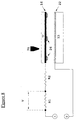
- FIG. 7 shows a touchscreen 10 according to the present invention.
- the first substrate (coversheet) 12 comprises a transparent polyethylene terephthalate (PET) sheet 14 and a conductive coating 16 disposed thereon.
- the conductive coating 16 has a conducting surface 18 facing away from the PET sheet 14.
- the conductive coating 16 of the first substrate comprises an intrinsically conductive polymer and is transparent.
- the touchscreen 10 shown in Figure 7 further comprises a second substrate 20.
- the second substrate 20 comprises a support and a conductive coating 22, which has a conductive surface 24 facing toward the conductive coating 16 of the first substrate and spaced apart therefrom.
- the conductive coating of the second support is made of ITO.
- the touchscreen 10 further comprises a plurality of spacer dots 26 of a type well known to the skilled artisan.
- the plurality of spacer dots 26 are disposed on the conductive surface 18 of the conductive coating 16 of the first substrate, facing the conductive surface 24 of the conductive coating 22 of the second substrate and spaced apart therefrom; alternatively, the spacer dots 26 may be disposed on the conductive surface 24 of the conductive coating 22 of the second substrate facing the conductive surface 18 of the conductive coating 16 of the first substrate and spaced apart therefrom.
- the touchscreen 10 further comprises a plurality of conductive elements electrically connected to the conductive coatings 16 and 22 to form an electrical circuit when the conductive coatings are in contact with each other.
- Wire 28 connects the first conductive coating 16 to a power source (not shown) within a computer monitor (not shown); similarly, wire 30 connects the second conductive coating 22 to a receiving medium (not shown) within the computer monitor (not shown).
- Many alternative configurations of conductive elements are possible, such as those described in US 4,306,110; US 5,438,168; US 5,541,370; US 5,589,857; US 5,818,430; and US 5,840,175; each of these is incorporated by reference.
- the intrinsically conductive polymers used in the present invention can be any intrinsically conductive polymer known in the art e.g. polyacetylene, polypyrrole, polyaniline, polythiophene, etc. Details about suitable intrinsically conductive polymers can be found in textbooks, such as "Advances in Synthetic Metals", ed. P. Bernier, S. Levers, and G. Bidan, Elsevier, 1999; “Intrinsically Conducting Polymers: An Emerging Technology", Kluwer (1993); “Conducting Polymer Fundamentals and Applications, A Practical Approach", P. Chandrasekhar, Kluwer, 1999; and “Handbook of Organic Conducting Molecules and Polymers", Ed. Walwa, Vol. 1-4, Marcel Dekker Inc. (1997).
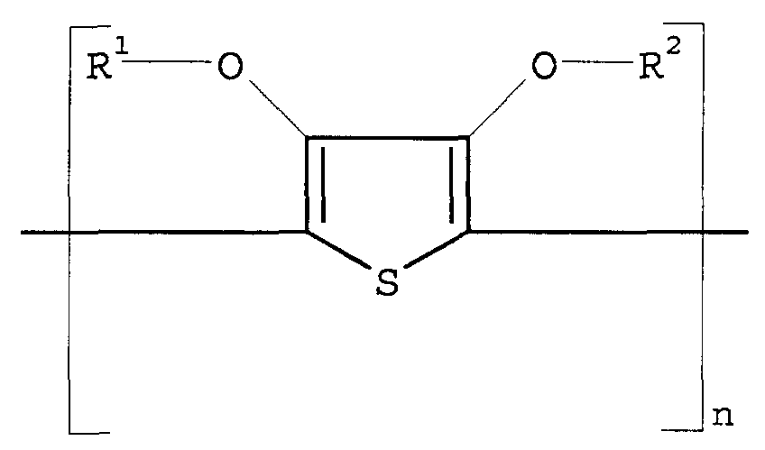
- the intrinsically conductive substituted or unsubstituted polythiophene has the following formula: wherein n is larger than 1, preferably larger than 5, and each of R 1 and R 2 independently represents hydrogen or an optionally substituted C 1-4 alkyl group or together represent an optionally substituted C 1-4 alkylene group or an optionally substituted cycloalkylene group, preferably an ethylene group, an optionally alkyl-substituted methylene group, an optionally C 1-12 alkyl- or phenyl-substituted ethylene group, a 1,3-propylene group or a 1,2-cyclohexylene group.
- a highly preferred substituted polythiophene is poly(3,4-ethylenedioxythiophene) (PEDOT), described in US 5,766,515 and EP-A 686 662, which are incorporated by reference.
- the conductive surface layers of the first and second substrates can be obtained by applying a coating solution or dispersion comprising the intrinsically conductive polymer using known coating methods, e.g. spin coating, dip coating, rod coating, blade coating, air knife coating, gravure coating, reverse roll coating, extrusion coating, slide coating and curtain coating.
- the coated solution or dispersion can be dried and cured using known methods. An overview of these coating techniques can be found in "Modern Coating and Drying Technology", Edward Cohen and Edgar B. Gutoff Editors, VCH publishers, Inc., New York (1992).
- the conductive coating thus obtained preferably has a surface resistivity ⁇ 50000 ⁇ /square.
- Stable aqueous polythiophene solutions or dispersions can be obtained by dissolving thiophenes corresponding to the formula above, a polyacid and an oxidising agent in an organic solvent or preferably in water, optionally containing a certain amount of organic solvent, and then stirring the resulting solution or emulsion at 0°C to 100°C until the polymerization reaction is completed.
- the polythiophenes formed by the oxidative polymerization are positively charged, the location and number of such positive charges being not determinable with certainty and therefore not mentioned in the general formula of the repeating units of the polythiophene polymer.
- the oxidising agents are those which are typically used for the oxidative polymerization of pyrrole, see e.g. J. Am. Soc. 85, 454 (1963).
- Preferred inexpensive and easy-to-handle oxidising agents are iron(III) salts, e.g. FeCl 3 , Fe(ClO 4 ) 3 and the iron(III) salts of organic acids and inorganic acids containing organic residues.
- Other suitable oxidising agents are H 2 O 2 , K 2 Cr 2 O 7 , alkali or ammonium persulfates, alkali perborates, potassium permanganate and copper salts such as copper tetrafluoroborate.
- Air or oxygen can also be used as oxidising agents.
- the polyacid forms a polyanion or, alternatively, the polyanion can be added as a salt of the corresponding polyacids, e.g. an alkali salt.
- Preferred polyacids or salts thereof are polymeric carbonic acids such as poly(acrylic acid), poly[(meth)-acrylic acid] and poly(maleic acid) or polymeric sulphonic acids such as poly(styrene sulphonic acid) (PSS) or poly(vinyl sulphonic acid).
- PSS poly(vinyl sulphonic acid).
- copolymers of such carbonic and/or sulphonic acids and of other polymerizable monomers such as styrene or acrylates can be used. PSS is especially preferred.
- the molecular weight of these polyanion forming polyacids is preferably between 1000 and 2x10 6 , more preferably between 2000 and 5x10 5 .
- These polyacids or their alkali salts are commercially available and can be prepared according to the known methods, e.g. as described in Houben-Weyl, Methoden der Organische Chemie, Bd. E20 Makromolekulare Stoffe, Mol 2, (1987), pp. 1141.
- the intrinsically conductive polymer solutions or dispersions thus obtained can then be used as basic ingredient of a coating solution or dispersion.
- the coating solution or dispersion can also comprise additional ingredients, such as one or more binders, one or more surfactants, spacing particles, UV-filters or IR-absorbers.
- Suitable polymer binders are described in EP-A 564 911. Such binders may be treated with a hardening agent, e.g. an epoxysilane as described in EP-A 564 911, which is especially suitable when coating on a glass substrate.
- the intrinsically conductive polymer coating solution or dispersion preferably also comprises is a linear, branched or cyclic aliphatic C 2-20 hydrocarbon or an optionally substituted aromatic C 6-14 hydrocarbon or a pyran or a furan, the organic compound comprising at least two hydroxy groups or at least one -COX or -CONYZ group wherein X denotes -OH and Y and Z independently of one another represent H or alkyl; or a heterocyclic compound containing at least one lactam group.
- organic compounds examples include N-methyl-2-pyrrolidone, 2-pyrrolidone, 1,3-dimethyl-2-imidazolidone, N,N,N',N'-tetramethylurea, formamide, dimethylformamide, and N,N-dimethylacetamide.
- sugar or sugar derivatives such as arabinose, saccharose, glucose, fructose and lactose, or di- or polyalcohols such as sorbitol, xylitol, mannitol, mannose, galactose, sorbose, gluconic acid, ethylene glycol, di- or tri(ethylene glycol), 1,1,1-trimethylol-propane, 1,3-propanediol, 1,5-pentanediol, 1,2,3-propanetriol, 1,2,4-butanetriol, 1,2,6-hexanetriol, or aromatic di- or polyalcohols such as resorcinol.
- sugar or sugar derivatives such as arabinose, saccharose, glucose, fructose and lactose
- di- or polyalcohols such as sorbitol, xylitol, mannitol, mannose, galactose, sorbose, gluconic acid,
- the switch and the electrical circuit can be used in any electrical device, such as a keyboard comprising membrane switches.
- a keyboard comprising membrane switches.
- the most preferred device is a resistive touchscreen.
- the standard AccuTouch® touchscreen configuration comprises a coversheet (first substrate) comprising a PET plastic sheet 32 coated with a transparent conductive coating 16 made of ITO and a glass support 33 coated with a transparent conductive coating 22 also made of ITO.
- the two transparent conductive coatings face each other and are spaced apart. Spacer dots were disposed on the coating of the coversheet (first substrate), facing, but not touching, the conductive coating of the glass screen.
- the standard configuration described above was modified for these experiments by replacing the ITO of the transparent conductive coating of the coversheet (first substrate) with a coating of an intrinsically conductive polymer.
- the particular intrinsically conductive polymer used was PEDOT/PSS, which is commercially available as a coating on 175 micrometer thick polyethylene terephthalate film under the trade name ORGACONTMEL3TG, of Agfa-Gevaert N.V., Mortsel, Belgium.
- a pneumatic piston was mounted above the first substrate on the side opposite the conductive surface and applied a load of 340 g (twelve ounces) to a stylus at a frequency of three times per second.
- the stylus 31 was made from a hard plastic, specifically CYCOLACTM T4500 ABS, which is commercially available from the General Electric Company.
- the tip radius of the stylus was 0.76 mm (0.030 inches). The tip was carefully positioned to strike the surface of the first substrate opposite to the conductive surface in the centre of an area defined by four of the plurality of spacer dots. When the stylus tip struck the first substrate, the conductive coatings on the first and second substrates of the touchscreen were pressed into contact, thus completing the electrical circuit.
- a 1000 ohm resistor R1 and a 9000 ohm resistor R2 were connected in series with the conductive coating of the first substrate as indicated in Figure 8.
- a data acquisition system was used to continuously monitor the voltage drop, V, across the resistor R1.
- the circuit also included a pair of input terminals A and B.
- Touchscreen failure can occur when the electrical contact is degraded to the extent that an appropriate electrical circuit is not completed when the conductive surfaces are brought into contact.
- a fifty percent reduction in current as indicated by a fifty percent decrease in the voltage drop across resistor R1, is a reasonable indication of touchscreen failure.
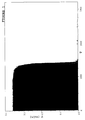
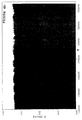
- Figure 1 shows that a fifty percent reduction in voltage, V, across resistor R1 was measured after approximately 1400 touches, T.
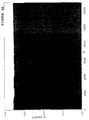
- terminal A again had a negative polarity (similar to Experiment 2), but the voltage potential across the input terminals A and B was reduced from 5 volts DC to 0.5 volt DC.
- Figures 4a and 4b show that a fifty percent reduction in voltage, V, across resistor R1 was not measured during the entire experiment, which lasted for more than 1.3 million touches, T.
Abstract
Description
- The present invention relates generally to switches. More specifically, the present invention relates to switches of the sort in which two conductive surfaces touch, such as in membrane switches and resistive touchscreens.
- Switches of the sort in which two conductive surfaces touch are used in such technologies as resistive touchscreens and membrane switches. For reasons of convenience and clarity, this background section describes touchscreens.
- Touchscreens are used in the computer arts to input data. Rather than a user of a computer inputting data by using a keyboard or a mouse, the user inputs data via a touchscreen mounted on the monitor of the computer. US 4,306,110; US 5,438,168; US 5,541,370; US 5,589,857; US 5,818,430; and US 5,840,175 disclose resistive touchscreens.
- The basic configuration of a resistive touchscreen comprises a first flexible substrate (coversheet) and a second substrate to which the coversheet is bonded. The first substrate typically comprises a thin layer of a plastic, such as poly(ethylene terephthalate) (PET). The first substrate has opposed first and second surfaces, the first surface facing a user of the computer and the second surface facing the second substrate. The second surface of the first substrate is conductive e.g. by coating with a conductive element. The second substrate generally comprises glass, although other transparent plastic materials could be used, and is either flat or curved to fit the curvature of a computer monitor. The second substrate has a conductive surface e.g. by coating with a conductive element facing the first substrate, and thus also facing a user of the computer.
- The conductive elements typically are transparent conductive coatings of thin layers of metals or metal oxides such as indium tin oxide (ITO), although other metals or metal oxides could be used. The composition and application of ITO coatings are described in US 5,776,373; US 5,851,642; and US 6,042,752.
- The touchscreen typically also comprises a plurality of spacer dots applied to the conductive coating on one of the facing surfaces, either of the coversheet (first substrate) or of the second substrate. Spacer dots are described in US 5,220,136, although other spacer dots could also be used. These spacer dots separate the coversheet (first substrate) from the second substrate. Touching the coversheet presses the two conductive surfaces, one on the coversheet (first substrate) and one on the second substrate, together and thereby completes an electrical circuit that also comprises conductive elements such as wires on the edges of the conductive surfaces. The specific location that is touched, and thus the location of the conductive surfaces that come into contact, is the data created and transmitted by the touch.
- EP-
A 0 128 529 discloses a pressure switch with two contact elements, which are arranged electrically separately from one another and are provided with connections, and additionally an electrically conductive bridging element, which is electrically insulated from one or both of these contact elements and is capable of being brought into contact with this or these by applying pressure, characterized in that the bridging element comprises an electrically conductive pyrrole polymer. - A problem with traditional touchscreens is the interrelationship between the mechanical properties of the flexible sheet of the coversheet (first substrate) and the conductive surface of the first substrate. The traditional materials used for the conductive surface are generally brittle and can crack and disbond from the flexible plastic sheet of the first substrate when it is deformed repeatedly. This in turn destroys the continuity of the electrical current carrying pathways in the conductive surface, which in turn results in failure of the touchscreen to accurately report the location of a touch. What is needed is a conductive surface that is flexible and durable and will bond to the flexible sheet for the life of the switch. When used in touchscreens, the conductive surface also needs to be transparent.
- In addition to the aforementioned shortcomings of metal and metal oxide coatings, ITO coatings have a limited lifespan, i.e. they fail to transmit the requisite electrical current after a number of touches. ITO coatings are also relatively expensive and have low resistance to mechanical damage. What is needed is a transparent conductive coating that has a longer lifespan, a low cost, and is resistant to mechanical damage.
- It is an aspect of the present invention to provide a switch wherein the conductive surface is inexpensive and has improved mechanical properties, i.e. is not brittle and which bonds to the flexible sheet of the first substrate even after long use.
- It is a further aspect of the present invention to provide touchscreens with an increased lifespan.
- Further aspects and advantages of the invention will become apparent from the description hereinafter.
- The present invention solves the above problems by changing both the material used in the transparent conductive surface of the first substrate (coversheet) and the electrical characteristics of the electrical circuit.
- In a first improvement over traditional touchscreen technology, the present invention uses a layer of an intrinsically conductive polymer as the coating on the flexible plastic sheet of the first substrate (coversheet). Intrinsically conductive polymer coatings on flexible plastic sheets are less brittle, more flexible to mechanical damage, and available at lower cost than ITO coatings on plastic sheets of first substrates (coversheets). Furthermore, by coating the plastic sheet with an intrinsically conductive polymer coating rather than a metallic coating, the coating does not crack or disbond from the plastic sheet of the first substrate (coversheet), and thus has a longer life. It has been discovered by the present inventors that, although the above switch is not liable to mechanical damage after long use, its lifetime may be limited when only one of the conductive coatings comprises an intrinsically conductive polymer and the other essentially consists of metal or metal oxide such as ITO. In order to enjoy the benefits of the improved mechanic properties of intrinsically conductive coatings over metal or metal oxide coatings it has been surprisingly discovered that it is necessary to control carefully the excitation of the electric circuit used with touchscreens incorporating intrinsically conductive polymers. This careful control of the excitation of the electric circuit is not required with conventional metal or metal oxide coatings such as ITO, and does not provide any additional advantage for these conventional materials. In particular, both the level of the excitation voltage and the polarity of the voltage applied to the intrinsically conductive polymer coating must be carefully controlled to maximize the benefit of the improved mechanical properties of the intrinsically conductive polymer coatings. The excitation voltage of the touchscreen must be reduced from the 5 volts DC that is commonly used with many commercially available touchscreens. The same effect is also observed with AC voltage. Additionally, the durability of the touchscreen is significantly improved when the intrinsically conductive polymer coating is held at a DC voltage. These surprising effects are not observed with conventional metal or metal oxide coatings.
- Aspects of the present invention are realized by a switch comprising: a first substrate (coversheet) having a conductive surface, the first substrate comprising an intrinsically conductive polymer, and a second substrate comprising a conductive surface, the substrate spaced apart from the first substrate, wherein movement of the coversheet into contact with the conductive surface of the second substrate generates a signal indicative of the contact, characterized in that the intrinsically conductive polymer is a substituted or unsubstituted polythiophene.
- Aspects of the present invention are further realized by an electrical circuit comprising the above-disclosed switch and a voltage source for applying a voltage difference between the conductive surface of the first substrate and the conductive surface of the second substrate.
- Aspects of the present invention are also realized by an electrical device comprising the above-disclosed switch or the above-disclosed electrical circuit.
- Aspects of the present invention are also realized by a touchscreen comprising the above-disclosed switch or the above-disclosed electrical circuit.
- Aspects of the present invention are also realized by a keyboard comprising the above-disclosed switch or the above-disclosed electrical circuit.
- Preferred embodiments of the switch and the electrical circuit according to the present invention are defined in the dependent claims.
-
- Figure 1 is a chart showing the voltage, V, across resistor R1 as a function of the number of touches, T, of Experiment 1 performed with the test device of Figure 8 with a circuit voltage of 5V and the coversheet (first substrate) having a positive polarity.
- Figure 2 is a chart showing the voltage, V, across resistor R1 as a function of the number of touches, T, of Experiment 2 performed with the test device of Figure 8 with a circuit voltage of 5V and the coversheet (first substrate) having a negative polarity.
- Figure 3a and Figure 3b are charts showing the voltage, V, across resistor R1 as a function of the number of touches, T, of Experiment 3 performed with the test device of Figure 8 with a circuit voltage of 0.5V and the coversheet (first substrate) having a positive polarity.
- Figure 4a and Figure 4b are charts showing the voltage, V, across resistor R1 as a function of the number of touches, T, of Experiment 4 performed with the test device of Figure 8 with a circuit voltage of 0.5V and the coversheet (first substrate) having a positive polarity.
- Figure 5 is a chart showing the voltage, V, across resistor R1 as a function of the number of touches, T, of Experiment 5 performed with the test device of Figure 8 with a circuit AC voltage of 5V and 60 Hz.
- Figure 6 is a chart showing the voltage, V, across resistor R1 as a function of the number of touches, T, of Experiment 6 performed with the test device of Figure 8 with a circuit AC voltage of 0.5V and 60 Hz.
- Figure 7 is a schematic diagram of a touchscreen in accordance with the present invention.
- Figure 8 is a schematic diagram of a circuit device used in accordance with the present invention.
-
- A first substrate being flexible and having a conductive surface, according to the present invention, is also indicated when the term coversheet is used.
- The switch of the present invention comprises a first and a second substrate. The first substrate (coversheet) of the switch comprises a flexible support (first support) and an intrinsically conductive substituted or unsubstituted polythiophene, is flexible and has a conductive surface. The second substrate of the switch comprises a support (second support) and has a conductive surface.
- According to a first embodiment of the switch of the present invention, wherein the conductive surfaces of the first and second substrates are mutually spaced apart and face one another, such that upon touching the first substrate the conductive surface thereof and the conductive surface of the second substrate are capable of being pressed together to realize an electrical contact.
- According to a second embodiment of the switch of the present invention, a first terminal extends from the conductive surface of the first substrate, and a second terminal extends from the conductive surface of the second substrate, the first terminal forming an electrical circuit such that the circuit is completed when movement of the first substrate brings the conductive surface of the first substrate into contact with the conductive surface of the second substrate.
- According to an third embodiment of the switch of the present invention, an electrical circuit comprising a voltage source for applying a voltage difference between the surface layer of the first substrate and the surface layer of the second substrate is completed when the first substrate is touched such that the surface layer of the first substrate and the surface layer of the second substrate are pressed together.
- According to a fourth embodiment of the switch of the present invention, the polarity of the conductive layer of the first substrate is negative relative to the conductive surface of the second substrate.
- According to a fourth embodiment of the switch according to the present invention, the conductive surface of the second substrate is a conventional inorganic conductive coating such as ITO.
- According to a fifth embodiment of the switch of the present invention, the switch further comprises a plurality of spacer dots disposed on the conductive surface of the first substrate or the conductive surface of the second substrate.
- According to a sixth embodiment of the switch of the present invention comprises:
a first substrate (coversheet) comprising a first support and a first conductive coating applied to a first surface of the first support, the first conductive coating comprising an intrinsically conductive substituted or unsubstituted thiophene; and a second substrate comprising a second support and a second conductive coating applied to a first surface of the second support;
wherein the first and second substrates are positioned such that the first and second conductive coatings face each other and an electric potential of less than five volts is applied across the first and the second conductive coatings. - Other elements, such as tie-layers between the plastic sheet and conductive polymer layer of the first substrate (coversheet) to improve adhesion (not shown), may also be used with the present invention.
- The first substrate (coversheet) of the switch of the present invention comprises a flexible support (first support) and an intrinsically conductive substituted or unsubstituted polythiophene, is flexible and has a conductive surface. Furthermore, the conductive surface of the first substrate comprises an intrinsically conductive substituted or unsubstituted polythiophene.
- The intrinsically conductive substituted or unsubstituted polythiophene of the first substrate can be provided by standard coating techniques or lamination. The flexible support (first support) of the first substrate used in the present invention is preferably a plastic sheet such as poly(ethylene terephthalate), poly(ethylene naphthalate), polystyrene, polyethersulphone, polycarbonate, polyacrylate, polyamide, polyimide, cellulosetriacetate, polyolefins, polyvinylchloride and other plastics having similar characteristics, which is optionally provided with a subbing layer.
- According to a preferred embodiment of the present invention, the conductive surface of the first substrate is the conductive surface of a conductive coating i.e. the first substrate comprises a support (first support) and a conductive coating.
- A flexible glass/plastic laminate such as described in WO 99/21707, WO 99/21708 and EP-A 1 013 413 provided with a conductive coating can also be used as the first substrate of the switch of the present invention.
- The first substrate is preferably substantially transparent i.e. is characterized by a white light transmission of at least 80%, more preferably at least 90% and most preferably at least 95%.
- The side opposite to the conductive coating of the first substrate can be provided with additional layers such as an anti-glare layer or a scratch-resistant hardcoat layer.
- The second substrate of the switch of the present invention comprises a support (second support) and has a conductive surface. The support (second support) of the second substrate is not required to be flexible and may be an inorganic substrate such as a ceramic or glass, although other transparent materials such as plastics may also be used.
- According to a preferred embodiment of the present invention, the conductive surface of the second substrate is the conductive surface of a conductive coating i.e. the second substrate comprises a support (second support) and a conductive coating.
- The second substrate may be flat or curved e.g. to fit the curvature of a computer monitor screen. The conductive surface of the second substrate can be indium tin oxide (ITO) or of other transparent metal or metal oxide coatings or of an intrinsically conductive polymer. The side opposite to the conductive coating of the second substrate can be provided with additional layers such as an anti-glare layer or a scratch-resistant hardcoat layer.
- An electrical circuit, according to the present invention, comprising the above-disclosed switch and a voltage source for applying a voltage difference between the conductive surface of the first substrate and the conductive surface of the second substrate. Such an electrical circuit is shown in Figure 8.
- According to a first embodiment of the electrical circuit of the present invention, the voltage source is an AC voltage source.
- According to a second embodiment of the electrical circuit of the present invention, the voltage source is a DC voltage source and wherein the conductive surface of the first substrate is connected to the negative polarity of the DC voltage source.
- According to a third embodiment of the electrical circuit of the present invention, wherein the voltage difference is less than five volts.
- According to a fourth embodiment of the electrical circuit of the present invention, wherein the voltage difference is less than three volts.
- According to a fifth embodiment of the electrical circuit of the present invention, wherein the voltage difference is less than one volt.
- A touchscreen comprising the switch, according to the present invention, or the electrical circuit, according to the present invention.
- According to a first embodiment of the touchscreen of the present invention, when using the switch of the present invention as a component of a touchscreen, a switch is preferred wherein the first substrate and the second substrate are substantially transparent, i.e. are each characterized by a white light transmission of at least 80%, more preferably at least 90% and most preferably at least 95%.
- According to a second embodiment of the touchscreen of the present invention, the touchscreen comprises:
- a first substrate (coversheet) comprising a first support, the first support comprising a plastic;
- a second substrate spaced apart from the first substrate;
- a first conductive coating on the first support, the first conductive coating having opposed surfaces, one of the opposed surfaces of the first conductive coating facing the first support, the other of the opposed surfaces of the first conductive coating facing the second substrate, the first conductive coating comprising an intrinsically conductive substituted or unsubstituted polythiophene;
- a second conductive coating on the second support, the second conductive coating spaced apart from the first conductive coating, the second conductive coating having a surface facing the first conductive coating and spaced apart therefrom; and
- a plurality of spacer dots, wherein:
- the plurality of spacer dots are disposed on the first conductive coating or the second conductive coating on the surface thereof facing the other of the conductive coatings, the spacer dots spaced apart from the other of the conductive coatings;
- a first terminal extending from the first conductive coating;
- a second terminal extending from the second conductive coating; and
- the first terminal, the first conductive coating, the second conductive coating, and the second terminal form an electrical circuit such that the electrical circuit is completed for transmission of an electrical signal to a receiving medium when the first conductive coating and the second conductive coating are pressed together.
-
- Figure 7 shows a
touchscreen 10 according to the present invention. The first substrate (coversheet) 12 comprises a transparent polyethylene terephthalate (PET)sheet 14 and aconductive coating 16 disposed thereon. Theconductive coating 16 has a conductingsurface 18 facing away from thePET sheet 14. Theconductive coating 16 of the first substrate comprises an intrinsically conductive polymer and is transparent. - The
touchscreen 10 shown in Figure 7 further comprises asecond substrate 20. Thesecond substrate 20 comprises a support and aconductive coating 22, which has aconductive surface 24 facing toward theconductive coating 16 of the first substrate and spaced apart therefrom. The conductive coating of the second support is made of ITO. - The
touchscreen 10 further comprises a plurality ofspacer dots 26 of a type well known to the skilled artisan. The plurality ofspacer dots 26 are disposed on theconductive surface 18 of theconductive coating 16 of the first substrate, facing theconductive surface 24 of theconductive coating 22 of the second substrate and spaced apart therefrom; alternatively, thespacer dots 26 may be disposed on theconductive surface 24 of theconductive coating 22 of the second substrate facing theconductive surface 18 of theconductive coating 16 of the first substrate and spaced apart therefrom. - The
touchscreen 10 further comprises a plurality of conductive elements electrically connected to theconductive coatings Wire 28 connects the firstconductive coating 16 to a power source (not shown) within a computer monitor (not shown); similarly,wire 30 connects the secondconductive coating 22 to a receiving medium (not shown) within the computer monitor (not shown). Many alternative configurations of conductive elements are possible, such as those described in US 4,306,110; US 5,438,168; US 5,541,370; US 5,589,857; US 5,818,430; and US 5,840,175; each of these is incorporated by reference. - The intrinsically conductive polymers used in the present invention can be any intrinsically conductive polymer known in the art e.g. polyacetylene, polypyrrole, polyaniline, polythiophene, etc. Details about suitable intrinsically conductive polymers can be found in textbooks, such as "Advances in Synthetic Metals", ed. P. Bernier, S. Lefrant, and G. Bidan, Elsevier, 1999; "Intrinsically Conducting Polymers: An Emerging Technology", Kluwer (1993); "Conducting Polymer Fundamentals and Applications, A Practical Approach", P. Chandrasekhar, Kluwer, 1999; and "Handbook of Organic Conducting Molecules and Polymers", Ed. Walwa, Vol. 1-4, Marcel Dekker Inc. (1997).
- According to a seventh embodiment of the switch of the present invention, the intrinsically conductive substituted or unsubstituted polythiophene has the following formula:wherein n is larger than 1, preferably larger than 5, and each of R1 and R2 independently represents hydrogen or an optionally substituted C1-4 alkyl group or together represent an optionally substituted C1-4 alkylene group or an optionally substituted cycloalkylene group, preferably an ethylene group, an optionally alkyl-substituted methylene group, an optionally C1-12 alkyl- or phenyl-substituted ethylene group, a 1,3-propylene group or a 1,2-cyclohexylene group. A highly preferred substituted polythiophene is poly(3,4-ethylenedioxythiophene) (PEDOT), described in US 5,766,515 and EP-A 686 662, which are incorporated by reference.
- The conductive surface layers of the first and second substrates can be obtained by applying a coating solution or dispersion comprising the intrinsically conductive polymer using known coating methods, e.g. spin coating, dip coating, rod coating, blade coating, air knife coating, gravure coating, reverse roll coating, extrusion coating, slide coating and curtain coating. The coated solution or dispersion can be dried and cured using known methods. An overview of these coating techniques can be found in "Modern Coating and Drying Technology", Edward Cohen and Edgar B. Gutoff Editors, VCH publishers, Inc., New York (1992). The conductive coating thus obtained preferably has a surface resistivity < 50000 Ω/square.
- The preparation of intrinsically conductive polythiophene and aqueous dispersions containing such a polythiophene and a polyanion is described in EP-A 440 957 and corresponding US 5,300,575. The preparation of polythiophene proceeds in the presence of polymeric polyanion compounds by oxidative polymerization of 3,4-dialkoxythiophenes or 3,4-alkylenedioxythiophenes according to the following formula:wherein R1 and R2 are as defined above.

- Stable aqueous polythiophene solutions or dispersions can be obtained by dissolving thiophenes corresponding to the formula above, a polyacid and an oxidising agent in an organic solvent or preferably in water, optionally containing a certain amount of organic solvent, and then stirring the resulting solution or emulsion at 0°C to 100°C until the polymerization reaction is completed. The polythiophenes formed by the oxidative polymerization are positively charged, the location and number of such positive charges being not determinable with certainty and therefore not mentioned in the general formula of the repeating units of the polythiophene polymer.
- The oxidising agents are those which are typically used for the oxidative polymerization of pyrrole, see e.g. J. Am. Soc. 85, 454 (1963). Preferred inexpensive and easy-to-handle oxidising agents are iron(III) salts, e.g. FeCl3, Fe(ClO4)3 and the iron(III) salts of organic acids and inorganic acids containing organic residues. Other suitable oxidising agents are H2O2, K2Cr2O7, alkali or ammonium persulfates, alkali perborates, potassium permanganate and copper salts such as copper tetrafluoroborate. Air or oxygen can also be used as oxidising agents. Theoretically, 2.25 equivalents of oxidising agent per mol of thiophene are required for the oxidative polymerization thereof (J. Polym. Sci. Part A, Polymer Chemistry, Vol. 26, p.1287, 1988). In practice, however, the oxidising agent is used in excess, for example, in excess of 0.1 to 2 equivalents per mol of thiophene.
- The polyacid forms a polyanion or, alternatively, the polyanion can be added as a salt of the corresponding polyacids, e.g. an alkali salt. Preferred polyacids or salts thereof are polymeric carbonic acids such as poly(acrylic acid), poly[(meth)-acrylic acid] and poly(maleic acid) or polymeric sulphonic acids such as poly(styrene sulphonic acid) (PSS) or poly(vinyl sulphonic acid). Alternatively, copolymers of such carbonic and/or sulphonic acids and of other polymerizable monomers such as styrene or acrylates can be used. PSS is especially preferred. The molecular weight of these polyanion forming polyacids is preferably between 1000 and 2x10⁶, more preferably between 2000 and 5x10⁵. These polyacids or their alkali salts are commercially available and can be prepared according to the known methods, e.g. as described in Houben-Weyl, Methoden der Organische Chemie, Bd. E20 Makromolekulare Stoffe, Teil 2, (1987), pp. 1141.
- The intrinsically conductive polymer solutions or dispersions thus obtained can then be used as basic ingredient of a coating solution or dispersion. The coating solution or dispersion can also comprise additional ingredients, such as one or more binders, one or more surfactants, spacing particles, UV-filters or IR-absorbers. Suitable polymer binders are described in EP-A 564 911. Such binders may be treated with a hardening agent, e.g. an epoxysilane as described in EP-A 564 911, which is especially suitable when coating on a glass substrate.
- The intrinsically conductive polymer coating solution or dispersion preferably also comprises is a linear, branched or cyclic aliphatic C2-20 hydrocarbon or an optionally substituted aromatic C6-14 hydrocarbon or a pyran or a furan, the organic compound comprising at least two hydroxy groups or at least one -COX or -CONYZ group wherein X denotes -OH and Y and Z independently of one another represent H or alkyl; or a heterocyclic compound containing at least one lactam group. Examples of such organic compounds are N-methyl-2-pyrrolidone, 2-pyrrolidone, 1,3-dimethyl-2-imidazolidone, N,N,N',N'-tetramethylurea, formamide, dimethylformamide, and N,N-dimethylacetamide. Preferred examples are sugar or sugar derivatives such as arabinose, saccharose, glucose, fructose and lactose, or di- or polyalcohols such as sorbitol, xylitol, mannitol, mannose, galactose, sorbose, gluconic acid, ethylene glycol, di- or tri(ethylene glycol), 1,1,1-trimethylol-propane, 1,3-propanediol, 1,5-pentanediol, 1,2,3-propanetriol, 1,2,4-butanetriol, 1,2,6-hexanetriol, or aromatic di- or polyalcohols such as resorcinol.
- The switch and the electrical circuit can be used in any electrical device, such as a keyboard comprising membrane switches. The most preferred device is a resistive touchscreen.
- A series of tests, described hereafter as Experiments 1 to 6 were carried out using the test device shown in Figure 8. This setup was configured by modifying a standard 26.4 cm (10.4 inch)-display incorporating an AccuTouch® touchscreen, which is commercially available from Elo Touchsystems, Inc. of Fremont, California. The standard AccuTouch® touchscreen configuration comprises a coversheet (first substrate) comprising a PET
plastic sheet 32 coated with a transparentconductive coating 16 made of ITO and aglass support 33 coated with a transparentconductive coating 22 also made of ITO. The two transparent conductive coatings face each other and are spaced apart. Spacer dots were disposed on the coating of the coversheet (first substrate), facing, but not touching, the conductive coating of the glass screen. - The standard configuration described above was modified for these experiments by replacing the ITO of the transparent conductive coating of the coversheet (first substrate) with a coating of an intrinsically conductive polymer. The particular intrinsically conductive polymer used was PEDOT/PSS, which is commercially available as a coating on 175 micrometer thick polyethylene terephthalate film under the trade name ORGACON™EL3TG, of Agfa-Gevaert N.V., Mortsel, Belgium.
- A pneumatic piston was mounted above the first substrate on the side opposite the conductive surface and applied a load of 340 g (twelve ounces) to a stylus at a frequency of three times per second. The
stylus 31 was made from a hard plastic, specifically CYCOLAC™ T4500 ABS, which is commercially available from the General Electric Company. The tip radius of the stylus was 0.76 mm (0.030 inches). The tip was carefully positioned to strike the surface of the first substrate opposite to the conductive surface in the centre of an area defined by four of the plurality of spacer dots. When the stylus tip struck the first substrate, the conductive coatings on the first and second substrates of the touchscreen were pressed into contact, thus completing the electrical circuit. A 1000 ohm resistor R1 and a 9000 ohm resistor R2 were connected in series with the conductive coating of the first substrate as indicated in Figure 8. A data acquisition system was used to continuously monitor the voltage drop, V, across the resistor R1. The circuit also included a pair of input terminals A and B. - In this experiment a voltage potential of 5 volts DC was applied across the input terminals A and B; this voltage is commonly used in the touchscreen industry. The voltage of terminal A was positive with respect to terminal B, as taught in US 5,766,515. If the electrical contact made by touching the conductive surface of the first substrate and the conductive surface of the second substrate into contact is degraded, the current flow during each contact will decrease and cause a decrease in the voltage drop across the series resistance.
- Touchscreen failure can occur when the electrical contact is degraded to the extent that an appropriate electrical circuit is not completed when the conductive surfaces are brought into contact. A fifty percent reduction in current, as indicated by a fifty percent decrease in the voltage drop across resistor R1, is a reasonable indication of touchscreen failure. Figure 1 shows that a fifty percent reduction in voltage, V, across resistor R1 was measured after approximately 1400 touches, T.
- In experiment 2, a voltage potential of 5 volts DC was also applied across the input terminals A and B; however, the polarity, as compared to Experiment 1, was reversed i.e. terminal A had a negative voltage with respect to terminal B. Figure 2 shows that a fifty percent reduction in voltage, V, across resistor R1 was not measured until after approximately 80,000 touches, T, corresponding to a 57-fold improvement over Experiment 1.
- In experiment 3, terminal A again had a positive polarity, but the voltage potential across the input terminals A and B was reduced from 5 volts DC to 0.5 volt DC. Figure 3a shows that the voltage reduction, V, across resistor R1 was negligible after approximately 130,000 touches, T. The experiment continued for a total of approximately 1.81 million touches, T. Figure 3b shows that the voltage decrease across the last 120,000 touches, T, of the test was only a few percent lower than the original voltage, V, shown in Figure 3a. A fifty percent reduction in voltage, V, across resistor R1 was not measured during the entire experiment, which lasted for more than 1.81 million touches, T.
- In experiment 4, terminal A again had a negative polarity (similar to Experiment 2), but the voltage potential across the input terminals A and B was reduced from 5 volts DC to 0.5 volt DC. Figures 4a and 4b show that a fifty percent reduction in voltage, V, across resistor R1 was not measured during the entire experiment, which lasted for more than 1.3 million touches, T.
- These experiments showed that, both reversing the polarity and reducing the DC voltage greatly increased the number of touches before the system fails. This was surprising and unexpected.
- In experiment 5, a 5 volt AC source operating at 60 Hz was coupled to the input terminals A and B. Figure 5 shows that after approximately 700 touches, T, the voltage, V, measured across resistor R1 was reduced by more than fifty percent.
- In experiment 6, the AC voltage level was reduced from 5 volts to 0.5 volts. Figure 6 shows that a fifty percent reduction in voltage, V, across resistor R1 was not measured during the entire experiment, which lasted for more than 30,000 touches, T.
- This experiment showed that, reducing the AC voltage greatly increased the number of touches, T, before the system fails. These results were surprising and unexpected.
- As a practitioner of ordinary skill in the art will realize, the present invention is capable of many variations, including, but not limited to, all variations of resistive touchscreens and membrane switches. All such variations to the invention come within the scope of the present invention.
Claims (19)
- A switch comprising:wherein movement of the coversheet into contact with the conductive surface of the second substrate generates a signal indicative of the contact,a first substrate (coversheet) having a conductive surface, the first substrate comprising an intrinsically conductive polymer, anda second substrate comprising a conductive surface, the substrate spaced apart from the first substrate,
characterized in that the intrinsically conductive polymer is a substituted or unsubstituted polythiophene. - A switch according to claim 1, wherein the conductive surfaces of the first and second substrates are mutually spaced apart and face one another, such that upon touching the first substrate the conductive surface thereof and the conductive surface of the second substrate are capable of being pressed together to realize an electrical contact.
- Switch according to any of the preceding claims, wherein the conductive surface of the first substrate is the conductive surface of a conductive coating.
- Switch according to any of the preceding claims, wherein the conductive surface of the second substrate is the conductive surface of a conductive coating.
- Switch according to any of the preceding claims, wherein a first terminal extends from the conductive surface of the first substrate, and a second terminal extends from the conductive surface of the second substrate, the first terminal forming an electrical circuit such that the circuit is completed when movement of the first substrate brings the conductive surface of the first substrate into contact with the conductive surface of the second substrate.
- Switch according to any of the preceding claims, wherein the polarity of the conductive surface of the first substrate is negative relative to the conductive surface of the second substrate.
- Switch according to any of the preceding claims further comprising a plurality of spacer dots disposed on the conductive surface of the first substrate or the conductive surface of the second substrate.
- Switch according to any of the preceding claims wherein the second substrate and/or the first substrate is transparent.
- Switch according to any of the preceding claims wherein the first substrate comprises a plastic sheet.
- Switch according to any of the preceding claims wherein the substituted or unsubstituted polythiophene has the following formula :wherein n is larger than 1 and each of R1 and R2 independently represents hydrogen or an optionally substituted C1-4 alkyl group or together represent an optionally substituted C1-4 alkylene group or an optionally substituted cycloalkylene group, preferably an ethylene group, an optionally alkyl-substituted methylene group, an optionally C1-12 alkyl- or phenyl-substituted ethylene group, a 1,3-propylene group or a 1,2-cyclohexylene group.

- An electrical circuit comprising a switch according to any of the preceding claims and a voltage source for applying a voltage difference between the conductive surface of the first substrate and the conductive surface of the second substrate.
- Electrical circuit according to claim 11, wherein the voltage source is an AC voltage source.
- Electrical circuit according to claim 11, wherein the voltage source is a DC voltage source and wherein the conductive surface of the first substrate is connected to the negative polarity of the DC voltage source.
- Electrical circuit according to any of claims 11 to 13, wherein the voltage difference is less than five volts.
- Electrical circuit according to any of claims 11 to 13, wherein the voltage difference is less than three volts.
- Electrical circuit according to any of claims 11 to 13, wherein the voltage difference is less than one volt.
- An electrical device comprising a switch according to any of claims 1 to 10 or an electrical circuit according to any of claims 11 to 16.
- A touchscreen comprising a switch according to any of claims 1 to 10 or an electrical circuit according to any of claims 11 to 16.
- A keyboard comprising a switch according to any of claims 1 to 10 or an electrical circuit according to any of claims 11 to 16.
Priority Applications (1)
| Application Number | Priority Date | Filing Date | Title |
|---|---|---|---|
| EP20010000267 EP1172831B1 (en) | 2000-07-12 | 2001-07-03 | Switch with at least one flexible conductive member |
Applications Claiming Priority (5)
| Application Number | Priority Date | Filing Date | Title |
|---|---|---|---|
| EP00202444 | 2000-07-12 | ||
| EP00202444 | 2000-07-12 | ||
| US614290 | 2000-07-12 | ||
| US09/614,290 US6469267B1 (en) | 2000-07-12 | 2000-07-12 | Switch with at least one flexible conductive member |
| EP20010000267 EP1172831B1 (en) | 2000-07-12 | 2001-07-03 | Switch with at least one flexible conductive member |
Publications (3)
| Publication Number | Publication Date |
|---|---|
| EP1172831A2 true EP1172831A2 (en) | 2002-01-16 |
| EP1172831A3 EP1172831A3 (en) | 2006-03-29 |
| EP1172831B1 EP1172831B1 (en) | 2012-10-24 |
Family
ID=27223367
Family Applications (1)
| Application Number | Title | Priority Date | Filing Date |
|---|---|---|---|
| EP20010000267 Expired - Lifetime EP1172831B1 (en) | 2000-07-12 | 2001-07-03 | Switch with at least one flexible conductive member |
Country Status (1)
| Country | Link |
|---|---|
| EP (1) | EP1172831B1 (en) |
Cited By (22)
| Publication number | Priority date | Publication date | Assignee | Title |
|---|---|---|---|---|
| WO2003100715A2 (en) * | 2002-05-20 | 2003-12-04 | 3M Innovative Properties Company | Capacitive touch screen with conductive polymer |
| US6809280B2 (en) | 2002-05-02 | 2004-10-26 | 3M Innovative Properties Company | Pressure activated switch and touch panel |
| US6846579B2 (en) | 2002-02-15 | 2005-01-25 | Eastman Kodak Company | Multilayer with radiation absorber and touch screen |
| US6933064B2 (en) | 2002-02-15 | 2005-08-23 | Eastman Kodak Company | Multilayer with spacers, touch screen and method |
| US7151532B2 (en) | 2002-08-09 | 2006-12-19 | 3M Innovative Properties Company | Multifunctional multilayer optical film |
| WO2007006833A3 (en) * | 2005-07-13 | 2007-04-12 | Fundacion Cidetec | Polythiophen-based distributed pressure sensors having a large surface area |
| US7227538B2 (en) | 2004-02-25 | 2007-06-05 | 3M Innovative Properties Company | Touch sensor with linearized response |
| US7260999B2 (en) | 2004-12-23 | 2007-08-28 | 3M Innovative Properties Company | Force sensing membrane |
| US7307624B2 (en) | 2003-12-30 | 2007-12-11 | 3M Innovative Properties Company | Touch sensor with linearized response |
| US7327352B2 (en) | 2002-06-14 | 2008-02-05 | 3M Innovative Properties Company | Linearized conductive surface |
| US7339579B2 (en) | 2003-12-15 | 2008-03-04 | 3M Innovative Properties Company | Wiring harness and touch sensor incorporating same |
| US7468199B2 (en) | 2004-12-23 | 2008-12-23 | 3M Innovative Properties Company | Adhesive membrane for force switches and sensors |
| US7509881B2 (en) | 2005-07-29 | 2009-03-31 | 3M Innovative Properties Company | Interdigital force switches and sensors |
| US7535462B2 (en) | 2005-06-02 | 2009-05-19 | Eastman Kodak Company | Touchscreen with one carbon nanotube conductive layer |
| US7593004B2 (en) | 2005-06-02 | 2009-09-22 | Eastman Kodak Company | Touchscreen with conductive layer comprising carbon nanotubes |
| US7645497B2 (en) | 2005-06-02 | 2010-01-12 | Eastman Kodak Company | Multi-layer conductor with carbon nanotubes |
| US7973771B2 (en) | 2007-04-12 | 2011-07-05 | 3M Innovative Properties Company | Touch sensor with electrode array |
| US8068186B2 (en) | 2003-10-15 | 2011-11-29 | 3M Innovative Properties Company | Patterned conductor touch screen having improved optics |
| US8264466B2 (en) | 2006-03-31 | 2012-09-11 | 3M Innovative Properties Company | Touch screen having reduced visibility transparent conductor pattern |
| US9442600B2 (en) | 2005-12-19 | 2016-09-13 | 3M Innovative Properties Company | Touch sensitive projection screen |
| US9933446B2 (en) | 2008-03-04 | 2018-04-03 | 3M Innovative Properties Company | Processing of biological growth media based on measured manufacturing characteristics |
| US10834786B2 (en) | 2016-01-12 | 2020-11-10 | 3M Innovative Properties Company | Heating tape and system |
Families Citing this family (1)
| Publication number | Priority date | Publication date | Assignee | Title |
|---|---|---|---|---|
| US8417013B2 (en) | 2008-03-04 | 2013-04-09 | 3M Innovative Properties Company | Information management in automated processing of biological growth media |
Citations (7)
| Publication number | Priority date | Publication date | Assignee | Title |
|---|---|---|---|---|
| US4444998A (en) * | 1981-10-27 | 1984-04-24 | Spectra-Symbol Corporation | Touch controlled membrane for multi axis voltage selection |
| EP0128529A2 (en) * | 1983-06-10 | 1984-12-19 | BASF Aktiengesellschaft | Pressure switch |
| US5177330A (en) * | 1988-09-19 | 1993-01-05 | Futaba Denshi Kogyo K.K. | Key board switch |
| US5220136A (en) * | 1991-11-26 | 1993-06-15 | Elographics, Inc. | Contact touchscreen with an improved insulated spacer arrangement |
| WO1996039707A1 (en) * | 1995-06-06 | 1996-12-12 | Raychem Corporation | Flexible electrode-bearing article |
| JPH11105417A (en) * | 1997-10-02 | 1999-04-20 | Oike Ind Co Ltd | Transparent conductive transfer material |
| EP1013413A1 (en) * | 1998-12-21 | 2000-06-28 | Agfa-Gevaert N.V. | Electroconductive glass laminate |
-
2001
- 2001-07-03 EP EP20010000267 patent/EP1172831B1/en not_active Expired - Lifetime
Patent Citations (7)
| Publication number | Priority date | Publication date | Assignee | Title |
|---|---|---|---|---|
| US4444998A (en) * | 1981-10-27 | 1984-04-24 | Spectra-Symbol Corporation | Touch controlled membrane for multi axis voltage selection |
| EP0128529A2 (en) * | 1983-06-10 | 1984-12-19 | BASF Aktiengesellschaft | Pressure switch |
| US5177330A (en) * | 1988-09-19 | 1993-01-05 | Futaba Denshi Kogyo K.K. | Key board switch |
| US5220136A (en) * | 1991-11-26 | 1993-06-15 | Elographics, Inc. | Contact touchscreen with an improved insulated spacer arrangement |
| WO1996039707A1 (en) * | 1995-06-06 | 1996-12-12 | Raychem Corporation | Flexible electrode-bearing article |
| JPH11105417A (en) * | 1997-10-02 | 1999-04-20 | Oike Ind Co Ltd | Transparent conductive transfer material |
| EP1013413A1 (en) * | 1998-12-21 | 2000-06-28 | Agfa-Gevaert N.V. | Electroconductive glass laminate |
Non-Patent Citations (1)
| Title |
|---|
| PATENT ABSTRACTS OF JAPAN vol. 1999, no. 09, 30 July 1999 (1999-07-30) & JP 11 105417 A (OIKE IND CO LTD), 20 April 1999 (1999-04-20) * |
Cited By (27)
| Publication number | Priority date | Publication date | Assignee | Title |
|---|---|---|---|---|
| US6846579B2 (en) | 2002-02-15 | 2005-01-25 | Eastman Kodak Company | Multilayer with radiation absorber and touch screen |
| US6933064B2 (en) | 2002-02-15 | 2005-08-23 | Eastman Kodak Company | Multilayer with spacers, touch screen and method |
| US6809280B2 (en) | 2002-05-02 | 2004-10-26 | 3M Innovative Properties Company | Pressure activated switch and touch panel |
| WO2003100715A3 (en) * | 2002-05-20 | 2004-10-21 | 3M Innovative Properties Co | Capacitive touch screen with conductive polymer |
| US7477242B2 (en) | 2002-05-20 | 2009-01-13 | 3M Innovative Properties Company | Capacitive touch screen with conductive polymer |
| WO2003100715A2 (en) * | 2002-05-20 | 2003-12-04 | 3M Innovative Properties Company | Capacitive touch screen with conductive polymer |
| US7327352B2 (en) | 2002-06-14 | 2008-02-05 | 3M Innovative Properties Company | Linearized conductive surface |
| US7151532B2 (en) | 2002-08-09 | 2006-12-19 | 3M Innovative Properties Company | Multifunctional multilayer optical film |
| US8068186B2 (en) | 2003-10-15 | 2011-11-29 | 3M Innovative Properties Company | Patterned conductor touch screen having improved optics |
| US7339579B2 (en) | 2003-12-15 | 2008-03-04 | 3M Innovative Properties Company | Wiring harness and touch sensor incorporating same |
| US8194044B2 (en) | 2003-12-15 | 2012-06-05 | 3M Innovative Properties Company | Wiring harness and touch sensor incorporating same |
| US7439963B2 (en) | 2003-12-30 | 2008-10-21 | 3M Innovative Properties Company | Touch sensor with linearized response |
| US7307624B2 (en) | 2003-12-30 | 2007-12-11 | 3M Innovative Properties Company | Touch sensor with linearized response |
| US7227538B2 (en) | 2004-02-25 | 2007-06-05 | 3M Innovative Properties Company | Touch sensor with linearized response |
| US7468199B2 (en) | 2004-12-23 | 2008-12-23 | 3M Innovative Properties Company | Adhesive membrane for force switches and sensors |
| US7260999B2 (en) | 2004-12-23 | 2007-08-28 | 3M Innovative Properties Company | Force sensing membrane |
| US7645497B2 (en) | 2005-06-02 | 2010-01-12 | Eastman Kodak Company | Multi-layer conductor with carbon nanotubes |
| US7593004B2 (en) | 2005-06-02 | 2009-09-22 | Eastman Kodak Company | Touchscreen with conductive layer comprising carbon nanotubes |
| US7535462B2 (en) | 2005-06-02 | 2009-05-19 | Eastman Kodak Company | Touchscreen with one carbon nanotube conductive layer |
| WO2007006833A3 (en) * | 2005-07-13 | 2007-04-12 | Fundacion Cidetec | Polythiophen-based distributed pressure sensors having a large surface area |
| US8294226B2 (en) | 2005-07-13 | 2012-10-23 | Fundacion Cidetec | Polythiophene-based large surface distributed pressure sensors |
| US7509881B2 (en) | 2005-07-29 | 2009-03-31 | 3M Innovative Properties Company | Interdigital force switches and sensors |
| US9442600B2 (en) | 2005-12-19 | 2016-09-13 | 3M Innovative Properties Company | Touch sensitive projection screen |
| US8264466B2 (en) | 2006-03-31 | 2012-09-11 | 3M Innovative Properties Company | Touch screen having reduced visibility transparent conductor pattern |
| US7973771B2 (en) | 2007-04-12 | 2011-07-05 | 3M Innovative Properties Company | Touch sensor with electrode array |
| US9933446B2 (en) | 2008-03-04 | 2018-04-03 | 3M Innovative Properties Company | Processing of biological growth media based on measured manufacturing characteristics |
| US10834786B2 (en) | 2016-01-12 | 2020-11-10 | 3M Innovative Properties Company | Heating tape and system |
Also Published As
| Publication number | Publication date |
|---|---|
| EP1172831B1 (en) | 2012-10-24 |
| EP1172831A3 (en) | 2006-03-29 |
Similar Documents
| Publication | Publication Date | Title |
|---|---|---|
| EP1172831B1 (en) | Switch with at least one flexible conductive member | |
| US6469267B1 (en) | Switch with at least one flexible conductive member | |
| KR101629060B1 (en) | Transparent conductive film, method for fabricating the same and touch panel with it | |
| JP4314623B2 (en) | Transparent conductive laminate and touch panel | |
| JP4419146B2 (en) | Transparent conductive laminate | |
| US7148439B2 (en) | High durability touch panel | |
| JP5069284B2 (en) | Increasing the lifetime of conducting polymers by voltage reversal | |
| JP4943091B2 (en) | Transparent conductive film, electrode plate for touch panel and touch panel | |
| CN103176680B (en) | Touch panel and manufacturing method of touch panel | |
| US20170029629A1 (en) | Scratch resistant touch sensor | |
| CN105793805A (en) | Composite polarizing plate-integrated touch sensing electrode and touch screen panel having same | |
| CN103176652A (en) | Touch screen and manufacturing method of touch screen | |
| KR20070042506A (en) | Composite transparent conductive substrate for touch panel and touch panel | |
| US20080135310A1 (en) | Polythiophene-based large surface distributed pressure sensors | |
| KR20140084880A (en) | Touch Panel | |
| CN105765510B (en) | Hybrid touch sensing electrode and touch-screen panel | |
| JP2012158736A (en) | Conductive polymer composition, and method for producing the same | |
| JP4974071B2 (en) | Transparent conductive film for touch panel | |
| JP5162615B2 (en) | Electrical circuit comprising a switch with at least one flexible conductive member and a DC voltage source | |
| WO2011105148A1 (en) | Transparent conductive film and organic electroluminescent element | |
| KR20180060802A (en) | Touch sensitive device and display device comprising the same | |
| JP5750908B2 (en) | Method for producing transparent conductive film, transparent conductive film and organic electroluminescence element | |
| JP5498537B2 (en) | Transparent conductive film, method for producing the same, and touch panel provided with the same | |
| JP4214063B2 (en) | Transparent conductive laminate and touch panel | |
| CN108132726B (en) | Touch sensitive element and display device comprising same |
Legal Events
| Date | Code | Title | Description |
|---|---|---|---|
| PUAI | Public reference made under article 153(3) epc to a published international application that has entered the european phase |
Free format text: ORIGINAL CODE: 0009012 |
|
| AK | Designated contracting states |
Kind code of ref document: A2 Designated state(s): AT BE CH CY DE DK ES FI FR GB GR IE IT LI LU MC NL PT SE TR |
|
| AX | Request for extension of the european patent |
Free format text: AL;LT;LV;MK;RO;SI |
|
| PUAL | Search report despatched |
Free format text: ORIGINAL CODE: 0009013 |
|
| AK | Designated contracting states |
Kind code of ref document: A3 Designated state(s): AT BE CH CY DE DK ES FI FR GB GR IE IT LI LU MC NL PT SE TR |
|
| AX | Request for extension of the european patent |
Extension state: AL LT LV MK RO SI |
|
| RIC1 | Information provided on ipc code assigned before grant |
Ipc: H01H 13/70 20060101ALI20060209BHEP Ipc: G06F 3/033 20060101AFI20060209BHEP |
|
| 17P | Request for examination filed |
Effective date: 20060929 |
|
| RAP1 | Party data changed (applicant data changed or rights of an application transferred) |
Owner name: ELO TOUCHSYSTEMS, INC. Owner name: AGFA-GEVAERT |
|
| AKX | Designation fees paid |
Designated state(s): DE FR GB |
|
| 17Q | First examination report despatched |
Effective date: 20090122 |
|
| RAP1 | Party data changed (applicant data changed or rights of an application transferred) |
Owner name: ELO TOUCHSYSTEMS, INC. Owner name: AGFA-GEVAERT N.V. |
|
| REG | Reference to a national code |
Ref country code: DE Ref legal event code: R079 Ref document number: 60147260 Country of ref document: DE Free format text: PREVIOUS MAIN CLASS: G06F0003033000 Ipc: G06F0003045000 |
|
| GRAP | Despatch of communication of intention to grant a patent |
Free format text: ORIGINAL CODE: EPIDOSNIGR1 |
|
| RIC1 | Information provided on ipc code assigned before grant |
Ipc: H01H 13/702 20060101ALI20120507BHEP Ipc: G06F 3/045 20060101AFI20120507BHEP Ipc: H01H 13/785 20060101ALI20120507BHEP |
|
| RAP1 | Party data changed (applicant data changed or rights of an application transferred) |
Owner name: TYCO ELECTRONICS CORPORATION Owner name: AGFA-GEVAERT N.V. |
|
| GRAS | Grant fee paid |
Free format text: ORIGINAL CODE: EPIDOSNIGR3 |
|
| GRAA | (expected) grant |
Free format text: ORIGINAL CODE: 0009210 |
|
| RAP1 | Party data changed (applicant data changed or rights of an application transferred) |
Owner name: AGFA-GEVAERT N.V. Owner name: ELO TOUCH SOLUTIONS, INC. |
|
| AK | Designated contracting states |
Kind code of ref document: B1 Designated state(s): DE FR GB |
|
| REG | Reference to a national code |
Ref country code: GB Ref legal event code: FG4D |
|
| REG | Reference to a national code |
Ref country code: DE Ref legal event code: R096 Ref document number: 60147260 Country of ref document: DE Effective date: 20121220 |
|
| PGFP | Annual fee paid to national office [announced via postgrant information from national office to epo] |
Ref country code: GB Payment date: 20130612 Year of fee payment: 13 |
|
| PGFP | Annual fee paid to national office [announced via postgrant information from national office to epo] |
Ref country code: FR Payment date: 20130701 Year of fee payment: 13 |
|
| PLBE | No opposition filed within time limit |
Free format text: ORIGINAL CODE: 0009261 |
|
| STAA | Information on the status of an ep patent application or granted ep patent |
Free format text: STATUS: NO OPPOSITION FILED WITHIN TIME LIMIT |
|
| 26N | No opposition filed |
Effective date: 20130725 |
|
| PGFP | Annual fee paid to national office [announced via postgrant information from national office to epo] |
Ref country code: DE Payment date: 20130612 Year of fee payment: 13 |
|
| REG | Reference to a national code |
Ref country code: DE Ref legal event code: R097 Ref document number: 60147260 Country of ref document: DE Effective date: 20130725 |
|
| REG | Reference to a national code |
Ref country code: DE Ref legal event code: R119 Ref document number: 60147260 Country of ref document: DE |
|
| GBPC | Gb: european patent ceased through non-payment of renewal fee |
Effective date: 20140703 |
|
| REG | Reference to a national code |
Ref country code: FR Ref legal event code: ST Effective date: 20150331 |
|
| PG25 | Lapsed in a contracting state [announced via postgrant information from national office to epo] |
Ref country code: DE Free format text: LAPSE BECAUSE OF NON-PAYMENT OF DUE FEES Effective date: 20150203 |
|
| REG | Reference to a national code |
Ref country code: DE Ref legal event code: R119 Ref document number: 60147260 Country of ref document: DE Effective date: 20150203 |
|
| PG25 | Lapsed in a contracting state [announced via postgrant information from national office to epo] |
Ref country code: FR Free format text: LAPSE BECAUSE OF NON-PAYMENT OF DUE FEES Effective date: 20140731 Ref country code: GB Free format text: LAPSE BECAUSE OF NON-PAYMENT OF DUE FEES Effective date: 20140703 |