EP1199802A2 - General-purpose logic module and cell using the same - Google Patents
General-purpose logic module and cell using the same Download PDFInfo
- Publication number
- EP1199802A2 EP1199802A2 EP01250367A EP01250367A EP1199802A2 EP 1199802 A2 EP1199802 A2 EP 1199802A2 EP 01250367 A EP01250367 A EP 01250367A EP 01250367 A EP01250367 A EP 01250367A EP 1199802 A2 EP1199802 A2 EP 1199802A2
- Authority
- EP
- European Patent Office
- Prior art keywords
- node
- general
- purpose logic
- logic module
- output
- Prior art date
- Legal status (The legal status is an assumption and is not a legal conclusion. Google has not performed a legal analysis and makes no representation as to the accuracy of the status listed.)
- Granted
Links
Images


Classifications
-
- H—ELECTRICITY
- H03—ELECTRONIC CIRCUITRY
- H03K—PULSE TECHNIQUE
- H03K19/00—Logic circuits, i.e. having at least two inputs acting on one output; Inverting circuits
- H03K19/02—Logic circuits, i.e. having at least two inputs acting on one output; Inverting circuits using specified components
- H03K19/173—Logic circuits, i.e. having at least two inputs acting on one output; Inverting circuits using specified components using elementary logic circuits as components
- H03K19/1733—Controllable logic circuits
- H03K19/1737—Controllable logic circuits using multiplexers
Definitions
- the present invention relates to a general-purpose logic module and a cell using the same. More particularly, the present invention relates to a basic circuit configuration of the general-purpose logic module and a structure of the cell.
- JP-A-Heisei 7-106949
- JP-A-Heisei 7-106949
- U.S. Patent No.5055718 entitled "LOGIC MODULE WITH CONFIGURABLE COMBINATIONAL AND SEQUENTIAL BLOCKS” discloses a "General Purpose Combination Logic Module”.
- the general-purpose logic module disclosed in this gazette, as shown in Fig. 1, is provided with a four-input multiplexer (MUX). This four-input multiplexer is constituted by combining three two-input multiplexers.
- MUX four-input multiplexer
- a two-input multiplexer of a non-inversion output type is composed of inverters of a first stage, transfer gates of a second stage and an inverter of a third stage, as shown in Fig. 2.
- the inputted signal is passed through the logic elements of the three stages until the signal is outputted.
- the four-input multiplexer shown in Fig. 1 is formed by using the two-input multiplexer having such configuration, the inputted signal is passed through the logic elements of six stages until the signal is outputted.
- the two-input multiplexer is an inversion output type
- the inverter of the third stage is removed.
- the two-input multiplexer of this inversion output type is used to configure the four-input multiplexer shown in Fig. 1, the inputted signal is passed through the logic elements of four stages until the signal is outputted.
- the four-input multiplexer can be formed by using inverters and transfer gates as shown in Fig. 3, without any usage of the two-input multiplexer shown in Fig. 2.
- this four-input multiplexer shown in Fig. 3 the inputted signal is passed through the logic elements of four stages until the signal is outputted.
- U.S. Patent No.5684412 discloses "CELL FORMING PART OF A COUSTOMIZABLE ARRAY".
- This general-purpose logic module is composed of a NAND gate, two two-input multiplexers A, A, and one two-input multiplexer LARGE, as shown in Fig. 4A.
- the two-input multiplexer A is composed of inverters of a first stage and transfer gates of a second stage, as shown in Fig. 4B.
- the two-input multiplexer LARGE is composed of transfer gates of a first gate and an inverter of a second stage, as shown in Fig. 4C.
- the signal inputted to the general-purpose logic module shown in Fig. 4A is outputted after passed through the logic elements composed of a maximum of four stages.
- JP-A-Heisei, 10-223902 discloses a "Semiconductor Integrated Circuit Apparatus".
- This semiconductor integrated circuit apparatus is provided with: a first region and a second region which are formed on an SOI substrate and are arranged parallel to and independently of each other; a first MOS transistor of a first channel type and a second MOS transistor of a second channel type in which they are formed on the first region, and their source diffusion layer regions and drain diffusion layers are connected to each other through a first diffusion layer wiring; and a third MOS transistor of the first channel type in which it is formed on the second region, and its source diffusion layer is connected to a source diffusion layer of the second MOS transistor, or its drain diffusion layer is connected to a drain diffusion layer of the second MOS transistor through a second diffusion layer wiring.
- Each of the above-mentioned general-purpose logic modules is provided with a multiplexer composed of the plurality of inputs and the plurality of stages, in which the plurality of two-input multiplexers are connected in serial at the plurality of stages.
- the desirable logic circuit is established by setting its input terminal to a logic value "1" (for example, a power supply potential) or a logic value "0" (for example, a ground potential).
- the above-mentioned conventional general-purpose logic modules are formed such that the two-input multiplexers are connected in serial at the plurality of stages.
- the number of the stages of the logic elements through which the signal is passed becomes large.
- the transfer gates are inserted in serial at the plurality of stages.
- the conventional general-purpose logic modules have the defect that a switching speed is slow, as compared with a configuration of a circuit, such as a gate array cell base IC or the like, which can be provided with a simple logic circuit.
- an object of the present invention is to provide a general-purpose logic module in which a switch can be carried out at a high speed, and a cell using the same.
- a general-purpose logic module is composed of: a first inverter in which an input is connected to a first node; a second node connected to an output of the first inverter; a second inverter in which an input is connected to a third node; a third inverter in which an input is connected to a fourth node; a first transfer gate in which an input is connected to the output of the first inverter, a first control input is connected to the fourth node, and a second control input is connected to an output of the third inverter; a second transfer gate in which an input is connected to the output of the second inverter, a first control input is connected to the output of the third inverter, and a second control input is connected to the fourth node; and a fifth node connected to an output of the first transfer gate and an output of the second transfer gate.
- a cell according to a second aspect of the present invention is composed of a first general-purpose logic module according to the first aspect of the present invention, a second general-purpose logic module and a third general-purpose logic module.
- the second general-purpose logic module includes a fourth inverter in which an input is connected to a seventh node and an output is connected to an eighth node.
- the third general-purpose logic module includes: a fifth inverter in which an input is connected to an eleventh node; a third transfer gate in which an input is connected to a ninth node, a first control input is inputted to the eleventh node, and a second control input is connected to an output of the fifth inverter; a fourth transfer gate in which an input is connected to a tenth node, a first control input is connected to an output of the fifth inverter, and a second control input is connected to the eleventh node; a sixth inverter in which an input is connected to an output of the third transfer gate and an output of the fourth transfer gate; and a twelfth node which is connected to an output of the sixth inverter.
- a general-purpose logic module is composed of: a first inverter in which an input is connected to a first node; a second inverter in which an input is connected to a third node; a sixth node which is connected to an output of the second inverter; a third inverter in which an input is connected to a fourth node; a first transfer gate in which an input is connected to an output of the first inverter, a first control input is connected to the fourth node, and a second control input is connected to an output of the third inverter; a second transfer gate in which an input is connected to an output of the second inverter, a first control input is connected to an output of the third inverter, and a second control input is connected to the fourth node; and a fifth node which is connected to an output of the first transfer gate and an output of the second transfer gate.
- a cell according to a fourth aspect of the present invention is composed of a first general-purpose logic module according to the third aspect of the present invention, a second general-purpose logic module and a third general-purpose logic module.
- the second general-purpose logic module includes a fourth inverter in which an input is connected to a seventh node and an output is connected to an eighth node.
- the third general-purpose logic module includes: a fifth inverter in which an input is connected to an eleventh node; a third transfer gate in which an input is connected to a ninth node, a first control input is inputted to the eleventh node, and a second control input is connected to an output of the fifth inverter; a fourth transfer gate in which an input is connected to a tenth node, a first control input is connected to an output of the fifth inverter, and a second control input is connected to the eleventh node; a sixth inverter in which an input is connected to an output of the third transfer gate and an output of the fourth transfer gate; and a twelfth node which is connected to an output of the sixth inverter.
- a first embodiment of the present invention is designed such that a general-purpose logic module has a multiplexer function by using a transfer gate and an inverter which are connected in series, and an output from the inverter can be used as a node.
- Fig. 5 is a circuit diagram showing the configuration of the general-purpose logic module according to the first embodiment of the present invention.
- This general-purpose logic module is composed of a two-input multiplexer of an inversion output type in which the first stage is the inverter and the second stage is the transfer gate.
- This general-purpose logic module is provided with: six nodes of a first node T1, a second node T2, a third node T3, a fourth node T4, a fifth node T5 and a sixth node T6; and five logic elements of a first inverter 10, a second inverter 11, a third inverter 12, a first transfer gate 20 and a second transfer gate 21.
- Each of the first to third inverters 10 to 12 has a known structure, for example, in which an N-channel MOS transistor and a P-channel MOS transistor are connected in serial with each other between a power supply and a ground, and an inputted signal is inverted and outputted.
- Each of those first to third inverters 10 to 12 is formed at a small size in order to reduce an input capacitance.
- Each of the first and second transfer gates 20, 21 has the structure in which the N-channel MOS transistor and the P-channel MOS transistor are connected parallel to each other, namely, the structure in which their sources are connected to each other and their drains are connected to each other.
- a signal supplied to an input terminal of the transfer gate is passed, or the pass of the signal is stopped.
- the gate of the P-channel MOS transistor is referred to as a first control input terminal
- the gate of the N-channel MOS transistor is referred to as a second control input terminal.
- the first node T1 is connected to an input terminal of the first inverter 10.
- An output terminal of the first inverter 10 is connected to an input terminal of the first transfer gate 20 and the second node T2.
- the third node T3 is connected to an input terminal of the second inverter 11.
- An output terminal of the second inverter 11 is connected to an input terminal of the second transfer gate 21 and the sixth node T6.
- the fourth node T4 is connected to an input terminal of the third inverter 12, the first control input terminal of the first transfer gate 20 and the second control input terminal of the second transfer gate 21.
- An output terminal of the third inverter 12 is connected to the second control input terminal of the first transfer gate 20 and the first control input terminal of the second transfer gate 21.
- An output terminal of the first transfer gate 20 and an output terminal of the second transfer gate 21 are connected to the fifth node T5.
- This general-purpose logic module basically functions as a multiplexer. That is, when a low level (hereafter, referred to as "L Level") signal is inputted to the fourth node T4, both of the P-channel MOS transistor and the N-channel MOS transistor constituting the first transfer gate 20 are turned on, and both the P-channel MOS transistor and the N-channel MOS transistor constituting the second transfer gate 21 are turned off. As a result, the signal inputted from the first node T1 is inverted by the first inverter 10, and outputted through the first transfer gate 20 from the fifth node T5.
- L Level low level
- H Level a high level (hereafter, referred to as "H Level") signal is inputted to the fourth node T4
- both of the P-channel MOS transistor and the N-channel MOS transistor constituting the first transfer gate 20 are turned off, and both the P-channel MOS transistor and the N-channel MOS transistor constituting the second transfer gate 21 are turned on.
- the signal inputted from the third node T3 is inverted by the second inverter 11, and outputted through the second transfer gate 21 from the fifth node T5.
- the function of the multiplexer of the inversion output type is attained. That is, depending on the level of the signal supplied to the fourth node T4, any one of the signal inputted to the first node T1 and the signal inputted to the third node T3 is inverted, and then outputted from the fifth node T5.
- this general-purpose logic module can be formed by removing the sixth node T6 from the general-purpose logic module shown in Fig. 5, as shown in Fig. 6, or by removing the second node T2 from the general-purpose logic module shown in Fig. 5, as shown in Fig. 7.
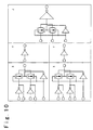
- a second embodiment of the present invention is a cell including the general-purpose logic module according to the first embodiment.
- Fig. 10 is a view showing the configuration of this cell.
- This cell is composed of the first general-purpose logic module X, a second general-purpose logic module Y and a third general-purpose logic module Z.
- the first general-purpose logic module X is the general-purpose logic module according to the first embodiment. It should be noted that, as for the cell shown in Fig. 10, for the purpose of easy illustration, the case is illustrated in which the number of the first general-purpose logic modules X is two, the number of the second general-purpose logic modules Y is two and the number of the third general-purpose logic module Z is one. However, the respective numbers of the general-purpose logic modules are arbitrary.
- the cell includes the first general-purpose logic module X, the second general-purpose logic module Y and the general-purpose logic module Z at a ratio of 2:2:1. However, it is not limited to this ratio.
- the second general-purpose logic module Y is constituted by a fourth inverter 13 in which a seventh node T7 is connected to an input terminal, and an eighth node T8 is connected to an output terminal, as shown in Fig. 8.
- the third general-purpose logic module Z is constituted by a two-input multiplexer of an inversion output type which is composed of transfer gates of a first stage and an inverter of a second stage, as shown in Fig. 9.
- This third general-purpose logic module Z is composed of: four nodes of a ninth node T9, a tenth node T10, an eleventh node T11 and a twelfth node T12; and four logic elements of a fifth inverter 15, a sixth inverter 15, a third transfer gate 22 and a fourth transfer gate 23.
- the fifth inverter 14 is equal to the first to third inverters 10 to 12 in the first embodiment.
- the sixth inverter 15 is formed at a larger size in order to improve the ability to drive, although having the same circuit structure and function as the first to third inverters 10 to 12.
- the third transfer gate 22 and the fourth transfer gate 23 are equal to the first transfer gate 20 and the second transfer gate in the first embodiment, respectively.
- the ninth node T9 is connected to an input terminal of the third transfer gate 22.
- An output terminal of the third transfer gate 22 is connected to an input terminal of the sixth inverter 15.
- the tenth node T10 is connected to an input terminal of the fourth transfer gate 23.
- An output terminal of the fourth transfer gate 23 is connected to the input terminal of the sixth inverter 15.
- the eleventh node T11 is connected to an input terminal of the fifth inverter 14, a first control input terminal of the third transfer gate 22 and a second control input terminal of the fourth transfer gate 23.
- An output terminal of the fifth inverter 14 is connected to a second control input terminal of the third transfer gate 22 and a first control input terminal of the fourth transfer gate 23.
- An output terminal of the sixth inverter 15 is connected to the twelfth node T12.
- This third general-purpose logic module Z basically functions as a multiplexer. That is, when a signal of the L level is inputted to the eleventh node T11, both of a P-channel MOS transistor and an N-channel MOS transistor constituting the third transfer gate 22 are turned on, and both a P-channel MOS transistor and an N-channel MOS transistor constituting the fourth transfer gate 23 are turned off. As a result, the signal inputted from the ninth node T9 is passed through the third transfer gate 22, and inverted by the sixth inverter 15, and then outputted from the twelfth node T12.
- both of the P-channel MOS transistor and the N-channel MOS transistor constituting the third transfer gate 22 are turned off, and both the P-channel MOS transistor and the N-channel MOS transistor constituting the fourth transfer gate 23 are turned on.
- the signal inputted from the tenth node T10 is passed through the fourth transfer gate 23, and inverted by the sixth inverter 15, and then outputted from the twelfth node T12.
- the function of the multiplexer of the inversion output type is attained. That is, depending on the level of the signal supplied to the eleventh node T11, any one of the signal inputted to the ninth node T9 and the signal inputted to the tenth node T12 is inverted, and then outputted from the twelfth node T12.
- Fig. 11 is an example in which the first general-purpose logic module X of the type shown in Fig. 5 is used to configure a NAND circuit.
- This NAND circuit is formed such that the first node T1 of the first general-purpose logic module X of the type shown in Fig. 5 is connected to the H level (logic "0") and the second node T2 and the sixth node T6 are set at a non-connection (N.C).
- N.C non-connection
- the inputted signal is passed through the logic elements of the four or six stages until the signal is outputted.
- the inputted signal is only passed through the logic elements of the two stages such as one inverter and one transfer gate.
- the inner gate delay implies the delay time substantially determined by the number of stages of the logic elements, except a wiring load capacitance occurring at an output end, a gate load capacitance and the like. It will be used below under the same meaning.
- this NAND circuit can be formed by using the first general-purpose logic module of the type shown in Fig. 6.
- the first node T1 is connected to the H level (logic "0"), and the second node T2 is set at non-connection.
- the two-input NAND circuit is attained in which the third node T3 (A) and the fourth node T4 (B) are used as input terminals and the fifth node T5 is used as output terminal (O).
- this NAND circuit can be formed by using the first general-purpose logic module of the type shown in Fig. 7.
- the first node T1 is connected to the H level (logic "0"), and the sixth node T6 is set at non-connection.
- the two-input NAND circuit is attained in which the third node T3 (A) and the fourth node T4 (B) are used as input terminals and the fifth node T5 is used as the output terminal (O).
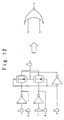
- Fig. 12 is an example in which the first general-purpose logic module of the type shown in Fig. 5 is used to configure an NOR circuit.
- This NOR circuit is formed such that the third node T3 of the first general-purpose logic module X is connected to the L level (logic "1"), and the second node T2 and the sixth node T6 are set at non-connection.
- the two-input NOR circuit is attained in which the first node T1 (A) and the fourth node T4 (B) are used as input terminals, and the fifth node T5 is used as output terminal (O).
- this NOR circuit can be formed by using the first general-purpose logic module of the type shown in Fig. 6.
- the third node T3 is connected to the L level (logic "1"), and the second node T2 is set at non-connection.
- the two-input NOR circuit is attained in which the first node T1 (A) and the fourth node T4 (B) are used as input terminals, and the fifth node T5 is used as output terminal (O).
- this NOR circuit can be formed by using the first general-purpose logic module of the type shown in Fig. 7.
- the third node T3 is connected to the L level (logic "1"), and the sixth node T6 is set at non-connection.
- the two-input NOR circuit is attained in which the third node T3 (A) and the fourth node T4 (B) are used as input terminals, and the fifth node T5 is used as output terminal (O).
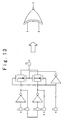
- Fig. 13 is an example in which the first general-purpose logic module of the type shown in Fig. 5 is used to configure an EXNOR circuit.
- This EXNOR circuit is formed such that the second node T2 and the third node T3 of the first general-purpose logic module X are connected to each other, and the sixth node T6 is set at non-connection.
- the two-input EXNOR circuit is attained in which the first node T1 (A) and the fourth node T4 (B) are used as input terminals, and the fifth node T5 is used as output terminal (O).
- this EXNOR circuit can be formed by using the first general-purpose logic module of the type shown in Fig. 6. In this case, the second node T2 and the third node T3 are connected to each other. Thus, the two-input EXNOR circuit is attained in which the first node T1 (A) and the fourth node T4 (B) are used as input terminals, and the fifth node T5 is used as output terminal (O).
- Fig. 14 is an example in which the first general-purpose logic module of the type shown in Fig. 5 is used to configure an EXOR circuit.
- This EXOR circuit is formed such that the first node T1 and the sixth node T6 of the first general-purpose logic module X are connected to each other, and the second node T2 is set at non-connection.
- the two-input EXOR circuit is attained in which the third node T3 (A) and the fourth node T4 (B) are used as input terminals, and the fifth node T5 is used as output terminal (O).
- this EXOR circuit can be formed by using the first general-purpose logic module of the type shown in Fig. 7. In this case, the first node T1 and the sixth node T6 are connected to each other. Thus, the two-input EXOR circuit is attained in which the third node T3 (A) and the fourth node T4 (B) are used as input terminals, and the fifth node T5 is used as output terminal (O).
- this EXOR circuit can be formed by using the first general-purpose logic module of the type shown in Fig. 6. In this case, the second node T2 and the third node T3 are connected to each other. Thus, the two-input EXOR circuit is attained in which the first node T1 (A) and the fourth node T4 (B) are used as input terminals, and the fifth node T5 is used as output terminal (O).
- Fig. 15 is an example in which a data latch circuit is formed by using one first general-purpose logic module X of the type shown in Fig. 5 and two second general-purpose logic modules Y.
- the fifth node T5 of the first general-purpose logic module X is connected to an input terminal of an inverter (hereafter, referred to as "first module” in this paragraph) that is one of the second general-purpose logic modules Y, and an output terminal of this first module is connected to the first node T1 of the first general-purpose logic module X. Also, the fifth node T5 of the first general-purpose logic module X is connected to an input terminal of an inverter (hereafter, referred to as "second module” in this paragraph) that is the other one of the second general-purpose logic modules Y.
- the data latch circuit is attained in which the third node T3 of the first general-purpose logic module X is used as a data input terminal (D), the fourth node T4 is used as an enable input terminal (G), and an output terminal of the second module is used as an output terminal (Q).
- This data latch circuit is constituted only by one two-input multiplexer of the inversion output type and two inverters. Thus, the latch circuit can be simply composed.
- Fig. 16 is an example in which a D-type flip-flop circuit is formed by using two first general-purpose logic modules X of the type shown in Fig. 5 and two second general-purpose logic modules Y.
- a fifth node T5 of a multiplexer (hereafter, referred to as "first Module” in this paragraph) that is one of the first general-purpose logic modules X is connected to a first node T1 of a multiplexer (hereafter, referred to as “second module” in this paragraph) that is the other one of the first general-purpose logic module X, and a fifth node T5 of this second module is connected to an input terminal of an inverter (hereafter, referred to as "third module") of an inverter that is one of the second general-purpose logic module Y, and an output terminal of this third module is connected to a first node T1 of the first module.
- a fifth node T5 of the second module is connected to an input terminal of an inverter (hereafter, referred to as "fourth module” in this paragraph) that is the other one of the second general-purpose logic module Y.
- the D-type flip-flop circuit is attained in which a third node T3 of the first module is used as a data input terminal (D), a fourth node T4 of the first module and a fourth node T4 of the second module are used as clock input terminals (C), and an output terminal of the fourth module is used as an output terminal (Q).
- This flip-flop circuit is constituted only by two two-input multiplexers of the inversion output type and two inverters. Thus, the flip-flop circuit can be simply composed.
- the function corresponding to that of the conventional four-input multiplexer can be formed by connecting one third general-purpose logic module Z to two first general-purpose logic modules X, and two two-input multiplexers of the typical non-inversion output type can be formed by connecting the second general-purpose logic module Y to two first general-purpose logic modules X, respectively.
- two two-input NAND circuits can be formed by using two first general-purpose logic modules X independently of each other, and apart from them, additional one two-input multiplexer of the non-inversion output type can be formed by connecting output terminals of two second general-purpose logic modules Y to input terminals of the third general-purpose logic modules Z, respectively.
- the second embodiment is designed so as to divide the configuration corresponding to the conventional four-input multiplexer into the multiplexer units of the two-input inversion output types, and individually pick up the output, and delete the number of the logic stages depending on the function, and also add the inverter and further connect the inner node of the two-input multiplexer of the inversion output type shown in Fig. 6 to another node.
- the optimal number of the logic stages it is possible to define the optimal number of the logic stages.
- the aspect that a plurality of logic functions can be attained is not lost, even when compared with the conventional four-input multiplexer.
- the third general-purpose logic module Z used in the second embodiment can be formed as shown in Fig. 17. That is, it may be formed such that the multiplexer portion and inverter portion of the third general-purpose logic module Z are separated from each other, and respective nodes are placed in the separated portions. This configuration can improve the generalization.
Abstract
Description
- The present invention relates to a general-purpose logic module and a cell using the same. More particularly, the present invention relates to a basic circuit configuration of the general-purpose logic module and a structure of the cell.
- Conventionally, a general-purpose logic module used in a typical field programmable gate array (FPGA) and a mask programmable gate array with a function block base have been well known. This general-purpose logic module is formed such that a designer can select one of a plurality of logic functions.
- As a general-purpose logic module provided with a multiplexer in which a plurality of combination logic functions can be selected, for example, Japanese Laid Open Patent Application (JP-A-Heisei, 7-106949) corresponding to U.S. Patent No.5055718 entitled "LOGIC MODULE WITH CONFIGURABLE COMBINATIONAL AND SEQUENTIAL BLOCKS" discloses a "General Purpose Combination Logic Module". The general-purpose logic module disclosed in this gazette, as shown in Fig. 1, is provided with a four-input multiplexer (MUX). This four-input multiplexer is constituted by combining three two-input multiplexers.
- This gazette does not clarify the configuration of the two-input multiplexer. Typically, a two-input multiplexer of a non-inversion output type is composed of inverters of a first stage, transfer gates of a second stage and an inverter of a third stage, as shown in Fig. 2. Thus, the inputted signal is passed through the logic elements of the three stages until the signal is outputted. If the four-input multiplexer shown in Fig. 1 is formed by using the two-input multiplexer having such configuration, the inputted signal is passed through the logic elements of six stages until the signal is outputted.
- It should be noted that, when the two-input multiplexer is an inversion output type, the inverter of the third stage is removed. Thus, if the two-input multiplexer of this inversion output type is used to configure the four-input multiplexer shown in Fig. 1, the inputted signal is passed through the logic elements of four stages until the signal is outputted.
- Moreover, the four-input multiplexer can be formed by using inverters and transfer gates as shown in Fig. 3, without any usage of the two-input multiplexer shown in Fig. 2. In the case of this four-input multiplexer shown in Fig. 3, the inputted signal is passed through the logic elements of four stages until the signal is outputted.
- Also, as another general-purpose logic module, U.S. Patent No.5684412 discloses "CELL FORMING PART OF A COUSTOMIZABLE ARRAY". This general-purpose logic module is composed of a NAND gate, two two-input multiplexers A, A, and one two-input multiplexer LARGE, as shown in Fig. 4A. The two-input multiplexer A is composed of inverters of a first stage and transfer gates of a second stage, as shown in Fig. 4B. The two-input multiplexer LARGE is composed of transfer gates of a first gate and an inverter of a second stage, as shown in Fig. 4C. Thus, the signal inputted to the general-purpose logic module shown in Fig. 4A is outputted after passed through the logic elements composed of a maximum of four stages.
- In addition to the above-mentioned general-purpose logic modules, a general-purpose logic module provided with a multiplexer in which a plurality of combination logic functions can be selected is disclosed in U.S. Patent No.4910417, U.S. Patent No.6014038 and the like.
- Japanese Laid Open Patent Application (JP-A-Heisei, 10-223902) discloses a "Semiconductor Integrated Circuit Apparatus". This semiconductor integrated circuit apparatus is provided with: a first region and a second region which are formed on an SOI substrate and are arranged parallel to and independently of each other; a first MOS transistor of a first channel type and a second MOS transistor of a second channel type in which they are formed on the first region, and their source diffusion layer regions and drain diffusion layers are connected to each other through a first diffusion layer wiring; and a third MOS transistor of the first channel type in which it is formed on the second region, and its source diffusion layer is connected to a source diffusion layer of the second MOS transistor, or its drain diffusion layer is connected to a drain diffusion layer of the second MOS transistor through a second diffusion layer wiring.
- Because of the above-mentioned configuration, it is possible to solve such conventional problems such as that a PN element separation region for arranging the bulk CMOS transistor is required, the connection using a metallic wiring is required to connect between the drain diffusion layers of an N-channel MOS transistor and a P-channel MOS transistor, and a wiring area within a block is increased.
- Each of the above-mentioned general-purpose logic modules is provided with a multiplexer composed of the plurality of inputs and the plurality of stages, in which the plurality of two-input multiplexers are connected in serial at the plurality of stages. The desirable logic circuit is established by setting its input terminal to a logic value "1" (for example, a power supply potential) or a logic value "0" (for example, a ground potential).
- However, the above-mentioned conventional general-purpose logic modules are formed such that the two-input multiplexers are connected in serial at the plurality of stages. Thus, the number of the stages of the logic elements through which the signal is passed becomes large. Moreover, the transfer gates are inserted in serial at the plurality of stages. For this reason, the conventional general-purpose logic modules have the defect that a switching speed is slow, as compared with a configuration of a circuit, such as a gate array cell base IC or the like, which can be provided with a simple logic circuit.
- Its difference is extreme if a comparison is done between the function of a two-input NAND, a two-input NOR, a two-input EXOR, a two-input EXNOR and the like which are constituted by using the general-purpose logic module shown in Fig. 1 or Fig. 4A and the function of those which are constituted by using the gate array cell base IC or the like. Especially, in a case of a configuration using a usual ASIC, the difference of an inner gate delay characteristic occurring in the two-input NAND, the two-input NOR and the like that can be constituted by one stage logic is evident.
- These problems are brought about because of a large number of logic element stages since the circuit configuration using the multiplexers composed of the plurality of inputs and the plurality of stages are employed such as the serial connection of the plurality of two-input multiplexers and because of the configuration of the logic circuit in which the plurality of transfer gates are inserted in serial.
- It is the object of the present invention to remove the above-mentioned problems. Therefore, an object of the present invention is to provide a general-purpose logic module in which a switch can be carried out at a high speed, and a cell using the same.
- In order to achieve the above-mentioned object, a general-purpose logic module according to a first aspect of the present invention is composed of: a first inverter in which an input is connected to a first node; a second node connected to an output of the first inverter; a second inverter in which an input is connected to a third node; a third inverter in which an input is connected to a fourth node; a first transfer gate in which an input is connected to the output of the first inverter, a first control input is connected to the fourth node, and a second control input is connected to an output of the third inverter; a second transfer gate in which an input is connected to the output of the second inverter, a first control input is connected to the output of the third inverter, and a second control input is connected to the fourth node; and a fifth node connected to an output of the first transfer gate and an output of the second transfer gate.
- In order to achieve the above-mentioned object, a cell according to a second aspect of the present invention is composed of a first general-purpose logic module according to the first aspect of the present invention, a second general-purpose logic module and a third general-purpose logic module. The second general-purpose logic module includes a fourth inverter in which an input is connected to a seventh node and an output is connected to an eighth node. The third general-purpose logic module includes: a fifth inverter in which an input is connected to an eleventh node; a third transfer gate in which an input is connected to a ninth node, a first control input is inputted to the eleventh node, and a second control input is connected to an output of the fifth inverter; a fourth transfer gate in which an input is connected to a tenth node, a first control input is connected to an output of the fifth inverter, and a second control input is connected to the eleventh node; a sixth inverter in which an input is connected to an output of the third transfer gate and an output of the fourth transfer gate; and a twelfth node which is connected to an output of the sixth inverter.
- In order to achieve the above-mentioned object, a general-purpose logic module according to a third aspect of the present invention is composed of: a first inverter in which an input is connected to a first node; a second inverter in which an input is connected to a third node; a sixth node which is connected to an output of the second inverter; a third inverter in which an input is connected to a fourth node; a first transfer gate in which an input is connected to an output of the first inverter, a first control input is connected to the fourth node, and a second control input is connected to an output of the third inverter; a second transfer gate in which an input is connected to an output of the second inverter, a first control input is connected to an output of the third inverter, and a second control input is connected to the fourth node; and a fifth node which is connected to an output of the first transfer gate and an output of the second transfer gate.
- In order to achieve the above-mentioned object, a cell according to a fourth aspect of the present invention is composed of a first general-purpose logic module according to the third aspect of the present invention, a second general-purpose logic module and a third general-purpose logic module. The second general-purpose logic module includes a fourth inverter in which an input is connected to a seventh node and an output is connected to an eighth node. The third general-purpose logic module includes: a fifth inverter in which an input is connected to an eleventh node; a third transfer gate in which an input is connected to a ninth node, a first control input is inputted to the eleventh node, and a second control input is connected to an output of the fifth inverter; a fourth transfer gate in which an input is connected to a tenth node, a first control input is connected to an output of the fifth inverter, and a second control input is connected to the eleventh node; a sixth inverter in which an input is connected to an output of the third transfer gate and an output of the fourth transfer gate; and a twelfth node which is connected to an output of the sixth inverter.
-
- Fig. 1 is a view illustrating a conventional general-purpose logic module;
- Fig. 2 is a circuit diagram showing a configuration of a multiplexer used in Fig. 1;
- Fig. 3 is a circuit diagram showing another configuration of the general-purpose logic module shown in Fig. 1;
- Figs. 4A to 4C are views describing another conventional general-purpose logic module;
- Fig. 5 is a circuit diagram showing a configuration of a general-purpose logic module according to a first embodiment of the present invention;
- Fig. 6 is a circuit diagram showing a variation of the general-purpose logic module shown in Fig. 5;
- Fig. 7 is a circuit diagram showing another variation of the general-purpose logic module shown in Fig. 5;
- Fig. 8 is a circuit diagram showing a configuration of a second general-purpose logic module used in a cell according to a second embodiment of the present invention;
- Fig. 9 is a circuit diagram showing a configuration of a third general-purpose logic module used in a cell according to a second embodiment of the present invention;
- Fig. 10 is a circuit diagram showing a configuration of the cell according to the second embodiment of the present invention;
- Fig. 11 is a view showing an example in which a NAND circuit is constituted by using the cell shown in Fig. 10;
- Fig. 12 is a view showing an example in which a NOR circuit is constituted by using the cell shown in Fig. 10;
- Fig. 13 is a view showing an example in which an EXNOR circuit is constituted by using the cell shown in Fig. 10;
- Fig. 14 is a view showing an example in which an EXOR circuit is constituted by using the cell shown in Fig. 10;
- Fig. 15 is a view showing an example in which a data latch circuit is constituted by using the cell shown in Fig. 10;
- Fig. 16 is a view showing an example in which a flip-flop circuit is constituted by using the cell shown in Fig. 10; and
- Fig. 17 is a view showing a configuration of a variation of the cell according to the second embodiment of the present invention.
-
- Now, the embodiments of the present invention will be described below with reference to the drawings.
- A first embodiment of the present invention is designed such that a general-purpose logic module has a multiplexer function by using a transfer gate and an inverter which are connected in series, and an output from the inverter can be used as a node.
- Fig. 5 is a circuit diagram showing the configuration of the general-purpose logic module according to the first embodiment of the present invention. This general-purpose logic module is composed of a two-input multiplexer of an inversion output type in which the first stage is the inverter and the second stage is the transfer gate. This general-purpose logic module is provided with: six nodes of a first node T1, a second node T2, a third node T3, a fourth node T4, a fifth node T5 and a sixth node T6; and five logic elements of a
first inverter 10, asecond inverter 11, athird inverter 12, afirst transfer gate 20 and asecond transfer gate 21. - Each of the first to
third inverters 10 to 12 has a known structure, for example, in which an N-channel MOS transistor and a P-channel MOS transistor are connected in serial with each other between a power supply and a ground, and an inputted signal is inverted and outputted. Each of those first tothird inverters 10 to 12 is formed at a small size in order to reduce an input capacitance. - Each of the first and
second transfer gates - The first node T1 is connected to an input terminal of the
first inverter 10. An output terminal of thefirst inverter 10 is connected to an input terminal of thefirst transfer gate 20 and the second node T2. - The third node T3 is connected to an input terminal of the
second inverter 11. An output terminal of thesecond inverter 11 is connected to an input terminal of thesecond transfer gate 21 and the sixth node T6. - The fourth node T4 is connected to an input terminal of the
third inverter 12, the first control input terminal of thefirst transfer gate 20 and the second control input terminal of thesecond transfer gate 21. An output terminal of thethird inverter 12 is connected to the second control input terminal of thefirst transfer gate 20 and the first control input terminal of thesecond transfer gate 21. - An output terminal of the
first transfer gate 20 and an output terminal of thesecond transfer gate 21 are connected to the fifth node T5. - The operation of the general-purpose logic module having the above-mentioned configuration will be described below. This general-purpose logic module basically functions as a multiplexer. That is, when a low level (hereafter, referred to as "L Level") signal is inputted to the fourth node T4, both of the P-channel MOS transistor and the N-channel MOS transistor constituting the
first transfer gate 20 are turned on, and both the P-channel MOS transistor and the N-channel MOS transistor constituting thesecond transfer gate 21 are turned off. As a result, the signal inputted from the first node T1 is inverted by thefirst inverter 10, and outputted through thefirst transfer gate 20 from the fifth node T5. - On the other hand, when a high level (hereafter, referred to as "H Level") signal is inputted to the fourth node T4, both of the P-channel MOS transistor and the N-channel MOS transistor constituting the
first transfer gate 20 are turned off, and both the P-channel MOS transistor and the N-channel MOS transistor constituting thesecond transfer gate 21 are turned on. As a result, the signal inputted from the third node T3 is inverted by thesecond inverter 11, and outputted through thesecond transfer gate 21 from the fifth node T5. - By the above-mentioned operation, the function of the multiplexer of the inversion output type is attained. That is, depending on the level of the signal supplied to the fourth node T4, any one of the signal inputted to the first node T1 and the signal inputted to the third node T3 is inverted, and then outputted from the fifth node T5.
- As necessary, this general-purpose logic module can be formed by removing the sixth node T6 from the general-purpose logic module shown in Fig. 5, as shown in Fig. 6, or by removing the second node T2 from the general-purpose logic module shown in Fig. 5, as shown in Fig. 7.
- A second embodiment of the present invention is a cell including the general-purpose logic module according to the first embodiment.
- Fig. 10 is a view showing the configuration of this cell. This cell is composed of the first general-purpose logic module X, a second general-purpose logic module Y and a third general-purpose logic module Z. The first general-purpose logic module X is the general-purpose logic module according to the first embodiment. It should be noted that, as for the cell shown in Fig. 10, for the purpose of easy illustration, the case is illustrated in which the number of the first general-purpose logic modules X is two, the number of the second general-purpose logic modules Y is two and the number of the third general-purpose logic module Z is one. However, the respective numbers of the general-purpose logic modules are arbitrary.
- It is desired that the cell includes the first general-purpose logic module X, the second general-purpose logic module Y and the general-purpose logic module Z at a ratio of 2:2:1. However, it is not limited to this ratio.
- The second general-purpose logic module Y is constituted by a
fourth inverter 13 in which a seventh node T7 is connected to an input terminal, and an eighth node T8 is connected to an output terminal, as shown in Fig. 8. - Also, the third general-purpose logic module Z is constituted by a two-input multiplexer of an inversion output type which is composed of transfer gates of a first stage and an inverter of a second stage, as shown in Fig. 9.
- This third general-purpose logic module Z is composed of: four nodes of a ninth node T9, a tenth node T10, an eleventh node T11 and a twelfth node T12; and four logic elements of a
fifth inverter 15, asixth inverter 15, athird transfer gate 22 and afourth transfer gate 23. - The
fifth inverter 14 is equal to the first tothird inverters 10 to 12 in the first embodiment. Thesixth inverter 15 is formed at a larger size in order to improve the ability to drive, although having the same circuit structure and function as the first tothird inverters 10 to 12. Also, thethird transfer gate 22 and thefourth transfer gate 23 are equal to thefirst transfer gate 20 and the second transfer gate in the first embodiment, respectively. - The ninth node T9 is connected to an input terminal of the
third transfer gate 22. An output terminal of thethird transfer gate 22 is connected to an input terminal of thesixth inverter 15. - The tenth node T10 is connected to an input terminal of the
fourth transfer gate 23. An output terminal of thefourth transfer gate 23 is connected to the input terminal of thesixth inverter 15. - The eleventh node T11 is connected to an input terminal of the
fifth inverter 14, a first control input terminal of thethird transfer gate 22 and a second control input terminal of thefourth transfer gate 23. An output terminal of thefifth inverter 14 is connected to a second control input terminal of thethird transfer gate 22 and a first control input terminal of thefourth transfer gate 23. An output terminal of thesixth inverter 15 is connected to the twelfth node T12. - The operation of the third general-purpose logic module Z having the above-mentioned configuration will be described below. This third general-purpose logic module Z basically functions as a multiplexer. That is, when a signal of the L level is inputted to the eleventh node T11, both of a P-channel MOS transistor and an N-channel MOS transistor constituting the
third transfer gate 22 are turned on, and both a P-channel MOS transistor and an N-channel MOS transistor constituting thefourth transfer gate 23 are turned off. As a result, the signal inputted from the ninth node T9 is passed through thethird transfer gate 22, and inverted by thesixth inverter 15, and then outputted from the twelfth node T12. - On the other hand, when a signal of the H level is inputted to the eleventh node T11, both of the P-channel MOS transistor and the N-channel MOS transistor constituting the
third transfer gate 22 are turned off, and both the P-channel MOS transistor and the N-channel MOS transistor constituting thefourth transfer gate 23 are turned on. As a result, the signal inputted from the tenth node T10 is passed through thefourth transfer gate 23, and inverted by thesixth inverter 15, and then outputted from the twelfth node T12. - By the above-mentioned operation, the function of the multiplexer of the inversion output type is attained. That is, depending on the level of the signal supplied to the eleventh node T11, any one of the signal inputted to the ninth node T9 and the signal inputted to the tenth node T12 is inverted, and then outputted from the twelfth node T12.
- An example will be described below in which the cell having the above-mentioned configuration is used to configure several logic circuits.
- Fig. 11 is an example in which the first general-purpose logic module X of the type shown in Fig. 5 is used to configure a NAND circuit.
- This NAND circuit is formed such that the first node T1 of the first general-purpose logic module X of the type shown in Fig. 5 is connected to the H level (logic "0") and the second node T2 and the sixth node T6 are set at a non-connection (N.C). Thus, the two-input NAND circuit is attained in which the third node T3 (A) and the fourth node T4 (B) are used as input terminals and the fifth node T5 is used as an output terminal (O).
- In the general-purpose logic module explained in the description of the related art, the inputted signal is passed through the logic elements of the four or six stages until the signal is outputted. On the contrary, according to this NAND circuit, the inputted signal is only passed through the logic elements of the two stages such as one inverter and one transfer gate. Thus, it is possible to shorten the time of the inner gate delay. It should be noted that the inner gate delay implies the delay time substantially determined by the number of stages of the logic elements, except a wiring load capacitance occurring at an output end, a gate load capacitance and the like. It will be used below under the same meaning.
- It should be noted that this NAND circuit can be formed by using the first general-purpose logic module of the type shown in Fig. 6. In this case, the first node T1 is connected to the H level (logic "0"), and the second node T2 is set at non-connection. Thus, the two-input NAND circuit is attained in which the third node T3 (A) and the fourth node T4 (B) are used as input terminals and the fifth node T5 is used as output terminal (O).
- Also, this NAND circuit can be formed by using the first general-purpose logic module of the type shown in Fig. 7. In this case, the first node T1 is connected to the H level (logic "0"), and the sixth node T6 is set at non-connection. Thus, the two-input NAND circuit is attained in which the third node T3 (A) and the fourth node T4 (B) are used as input terminals and the fifth node T5 is used as the output terminal (O).
- Fig. 12 is an example in which the first general-purpose logic module of the type shown in Fig. 5 is used to configure an NOR circuit.
- This NOR circuit is formed such that the third node T3 of the first general-purpose logic module X is connected to the L level (logic "1"), and the second node T2 and the sixth node T6 are set at non-connection. Thus, the two-input NOR circuit is attained in which the first node T1 (A) and the fourth node T4 (B) are used as input terminals, and the fifth node T5 is used as output terminal (O).
- According to this NOR circuit, similarly to the above-mentioned NAND circuit, the input signal is only passed through the logic elements of the two stages. Thus, it is possible to shorten the time of the inner gate delay.
- It should be noted that this NOR circuit can be formed by using the first general-purpose logic module of the type shown in Fig. 6. In this case, the third node T3 is connected to the L level (logic "1"), and the second node T2 is set at non-connection. Thus, the two-input NOR circuit is attained in which the first node T1 (A) and the fourth node T4 (B) are used as input terminals, and the fifth node T5 is used as output terminal (O).
- Also, this NOR circuit can be formed by using the first general-purpose logic module of the type shown in Fig. 7. In this case, the third node T3 is connected to the L level (logic "1"), and the sixth node T6 is set at non-connection. Thus, the two-input NOR circuit is attained in which the third node T3 (A) and the fourth node T4 (B) are used as input terminals, and the fifth node T5 is used as output terminal (O).
- Fig. 13 is an example in which the first general-purpose logic module of the type shown in Fig. 5 is used to configure an EXNOR circuit.
- This EXNOR circuit is formed such that the second node T2 and the third node T3 of the first general-purpose logic module X are connected to each other, and the sixth node T6 is set at non-connection. Thus, the two-input EXNOR circuit is attained in which the first node T1 (A) and the fourth node T4 (B) are used as input terminals, and the fifth node T5 is used as output terminal (O).
- According to this EXNOR circuit, although the inputted signal in the general-purpose logic module explained in the description of the related art is passed through the logic elements of the four or six stages until the signal is outputted, the input signal is only passed through the logic elements of the three stages such as the inverters of two stages and the transfer gate of one stage. Thus, it is possible to shorten the time of the inner gate delay.
- It should be noted that this EXNOR circuit can be formed by using the first general-purpose logic module of the type shown in Fig. 6. In this case, the second node T2 and the third node T3 are connected to each other. Thus, the two-input EXNOR circuit is attained in which the first node T1 (A) and the fourth node T4 (B) are used as input terminals, and the fifth node T5 is used as output terminal (O).
- Fig. 14 is an example in which the first general-purpose logic module of the type shown in Fig. 5 is used to configure an EXOR circuit.
- This EXOR circuit is formed such that the first node T1 and the sixth node T6 of the first general-purpose logic module X are connected to each other, and the second node T2 is set at non-connection. Thus, the two-input EXOR circuit is attained in which the third node T3 (A) and the fourth node T4 (B) are used as input terminals, and the fifth node T5 is used as output terminal (O).
- According to this EXOR circuit, although the inputted signal in the general-purpose logic module explained in the description of the related art is passed through the logic elements of the four or six stages until the signal is outputted, the inputted signal is only passed through the logic elements of the three stages such as the inverters of two stages and the transfer gate of one stage. Thus, it is possible to shorten the time of the inner gate delay.
- It should be noted that this EXOR circuit can be formed by using the first general-purpose logic module of the type shown in Fig. 7. In this case, the first node T1 and the sixth node T6 are connected to each other. Thus, the two-input EXOR circuit is attained in which the third node T3 (A) and the fourth node T4 (B) are used as input terminals, and the fifth node T5 is used as output terminal (O).
- Also, this EXOR circuit can be formed by using the first general-purpose logic module of the type shown in Fig. 6. In this case, the second node T2 and the third node T3 are connected to each other. Thus, the two-input EXOR circuit is attained in which the first node T1 (A) and the fourth node T4 (B) are used as input terminals, and the fifth node T5 is used as output terminal (O).
- Fig. 15 is an example in which a data latch circuit is formed by using one first general-purpose logic module X of the type shown in Fig. 5 and two second general-purpose logic modules Y.
- In this data latch circuit, the fifth node T5 of the first general-purpose logic module X is connected to an input terminal of an inverter (hereafter, referred to as "first module" in this paragraph) that is one of the second general-purpose logic modules Y, and an output terminal of this first module is connected to the first node T1 of the first general-purpose logic module X. Also, the fifth node T5 of the first general-purpose logic module X is connected to an input terminal of an inverter (hereafter, referred to as "second module" in this paragraph) that is the other one of the second general-purpose logic modules Y. Thus, the data latch circuit is attained in which the third node T3 of the first general-purpose logic module X is used as a data input terminal (D), the fourth node T4 is used as an enable input terminal (G), and an output terminal of the second module is used as an output terminal (Q).
- This data latch circuit is constituted only by one two-input multiplexer of the inversion output type and two inverters. Thus, the latch circuit can be simply composed.
- Fig. 16 is an example in which a D-type flip-flop circuit is formed by using two first general-purpose logic modules X of the type shown in Fig. 5 and two second general-purpose logic modules Y.
- In this flip-flop circuit, a fifth node T5 of a multiplexer (hereafter, referred to as "first Module" in this paragraph) that is one of the first general-purpose logic modules X is connected to a first node T1 of a multiplexer (hereafter, referred to as "second module" in this paragraph) that is the other one of the first general-purpose logic module X, and a fifth node T5 of this second module is connected to an input terminal of an inverter (hereafter, referred to as "third module") of an inverter that is one of the second general-purpose logic module Y, and an output terminal of this third module is connected to a first node T1 of the first module. Also, a fifth node T5 of the second module is connected to an input terminal of an inverter (hereafter, referred to as "fourth module" in this paragraph) that is the other one of the second general-purpose logic module Y. Thus, the D-type flip-flop circuit is attained in which a third node T3 of the first module is used as a data input terminal (D), a fourth node T4 of the first module and a fourth node T4 of the second module are used as clock input terminals (C), and an output terminal of the fourth module is used as an output terminal (Q).
- This flip-flop circuit is constituted only by two two-input multiplexers of the inversion output type and two inverters. Thus, the flip-flop circuit can be simply composed.
- It should be noted that, although not shown, the function corresponding to that of the conventional four-input multiplexer can be formed by connecting one third general-purpose logic module Z to two first general-purpose logic modules X, and two two-input multiplexers of the typical non-inversion output type can be formed by connecting the second general-purpose logic module Y to two first general-purpose logic modules X, respectively.
- Moreover, for example, two two-input NAND circuits can be formed by using two first general-purpose logic modules X independently of each other, and apart from them, additional one two-input multiplexer of the non-inversion output type can be formed by connecting output terminals of two second general-purpose logic modules Y to input terminals of the third general-purpose logic modules Z, respectively.
- As mentioned above, according to the second embodiment, it is designed so as to divide the configuration corresponding to the conventional four-input multiplexer into the multiplexer units of the two-input inversion output types, and individually pick up the output, and delete the number of the logic stages depending on the function, and also add the inverter and further connect the inner node of the two-input multiplexer of the inversion output type shown in Fig. 6 to another node. Thus, it is possible to define the optimal number of the logic stages. Hence, the aspect that a plurality of logic functions can be attained is not lost, even when compared with the conventional four-input multiplexer. Moreover, it is possible to increase the free degree of the circuit configuration.
- Incidentally, the third general-purpose logic module Z used in the second embodiment can be formed as shown in Fig. 17. That is, it may be formed such that the multiplexer portion and inverter portion of the third general-purpose logic module Z are separated from each other, and respective nodes are placed in the separated portions. This configuration can improve the generalization.
- As detailed above, according to the present invention, it is possible to provide a general-purpose logic module in which the switch can be carried out at the high speed, and the cell using the same.
Claims (28)
- A general-purpose logic module comprising:a first inverter (10) in which an input is connected to a first node (T1) ;a second inverter (11) in which an input is connected to a third node (T3);a node which is connected to an output of at lease one of said first inverter (10) and said second inverter (11);a third inverter (12) in which an input is connected to a fourth node (T4);a first transfer gate (20) in which an input is connected to the output of said first inverter (10), a first control input is connected to said fourth node (T4), and a second control input is connected to an output of said third inverter (12);a second transfer gate (21) in which an input is connected to an output of said second inverter (11), a first control input is connected to the output of said third inverter (12), and a second control input is connected to said fourth node (T4); anda fifth node (T5) which is connected to an output of said first transfer gate (20) and an output of said second transfer gate (21).
- The general-purpose logic module according to claim 1, wherein said node is a second node (T2) which is connected to the output of said first inverter (10).
- The general-purpose logic module according to claim 2, wherein a NAND circuit, in which said third node (T3) and said fourth node (T4) are used as inputs and said fifth node (T5) is used as an output, is formed by connecting said first node (T1) to a logic "0" and setting said second node (T2) at a non-connection.
- The general-purpose logic module according to claim 2, wherein a NOR circuit, in which said first node (T1) and said fourth node (T4) are used as inputs and said fifth node (T5) is used as an output, is formed by connecting said third node (T3) to a logic "1" and setting said second node (T2) at the non-connection.
- The general-purpose logic module according to claim 2, wherein an ENXOR circuit, in which said first node (T1) and said fourth node (T4) are used as inputs and said fifth node (T5) is used as an output, is formed by connecting said second node (T2) to said third node (T3).
- The general-purpose logic module according to claim 2, further comprising: a sixth node (T6) which is connected to the output of said second inverter (11).
- The general-purpose logic module according to claim 6, wherein an EXOR circuit, in which said third node (T3) and said fourth node (T4) are used as inputs and said fifth node (T5) is used as an output, is formed by connecting said first node (T1) to said sixth node (T6) and setting said second node (T2) at
non-connection. - A cell comprising:(A) a first general-purpose logic module according to claim 2;(B) a second general-purpose logic module including: a fourth inverter (13) in which an input is connected to a seventh node (T7) and an output is connected to an eighth node (T8); and(C) a third general-purpose logic module including:a fifth inverter (14) in which an input is connected to an eleventh node (T11);a third transfer gate (22) in which an input is connected to a ninth node (T9), a first control input is connected to said eleventh node (T11), and a second control input is connected to an output of said fifth inverter (14);a fourth transfer gate (23) in which an input is connected to a tenth node (T10), a first control input is connected to an output of said fifth inverter (14), and a second control input is connected to said eleventh node (T11);a sixth inverter (15) in which an input is connected to an output of said third transfer gate (22) and an output of said fourth transfer gate (23); anda twelfth node (T11) which is connected to an output of the sixth inverter (15).
- The cell according to claim 8, wherein said first general-purpose logic module is formed in a NAND circuit, in which said first node (T1) is connected to a logic "0" and said second node (T2) is set at a non-connection so that said third node (T3) and said fourth node (T4) are used as inputs and said fifth node (T5) is used as an output.
- The cell according to claim 8, wherein said first general-purpose logic module is formed in a NOR circuit, in which said third node (T3) is connected to a logic "1" and said second node (T2) is set at non-connection so that said first node (T1) and said fourth node (T4) are used as inputs and said fifth node (T5) is used as an output.
- The cell according to claim 8, wherein said first general-purpose logic module is formed in an EXNOR circuit, in which said second node (T2) is connected to said third node so that said first node (T1) and said fourth node (T4) are used as inputs and said fifth node (T5) is used as an output.
- The cell according to claim 8, wherein said first general-purpose logic module further comprises a sixth node (T6) which is connected to the output of said second inverter (11).
- The cell according to claim 12, wherein said first general-purpose logic module is formed in an EXOR circuit, in which said first node (T1) is connected to said sixth node (T6) and said second node (T2) is set at non-connection so that said third node (T3) and said fourth node (T4) are used as inputs and said fifth node (T5) is used as an output.
- The cell according to claim 8, wherein a latch circuit is formed by setting said second node (T2) of said first general-purpose logic module at a non-connection, and connecting said first node (T1) to said eighth node (T8) of a first module which is such a second general-purpose logic module, and connecting said fifth node (T5) to said seventh node (T7) of said first module and said seventh node (T7) of a second module which is also such a second general-purpose logic module, such that said third node (T3) of said first general-purpose logic module is used as a data input (D), and said fourth node (T4) is used as an enable input (G), and said eighth node (T8) of said second module is used as an output (Q).
- The cell according to claim 8, wherein a flip-flop circuit is formed by setting said second node (T2) of a first module which is such a first general-purpose logic module at the non-connection, connecting said first node (T1) of said first module to said second node (T2) of a second module which isalso such a first general-purpose logic module, connecting said fifth node (T5) of said first module to said first node (T1) of said second module, connecting said third node (T3) of said second module to said eighth node (T8) of a third module which issuch a second general-purpose logic module, and connecting said fifth node (T5) to said seventh node (T7) of said third module and said seventh node (T7) of a fourth module that is also such a second general-purpose logic module, such that a third node (T3) of said first module is used as a data input (D), and said fourth node (T4) of said first module and said fourth node (T4) of said second module are used as clock inputs (C), and said eighth node (T8) of said fourth module is used as an output (Q).
- The cell according to any one of claims 8 to 15, wherein said first general-purpose logic module, said second general-purpose logic module and said third general-purpose logic module are included at a ratio of 2:2:1.
- The general-purpose logic module according to claim 1, wherein said node is a sixth node (T6) which is connected to the output of said second inverter (11).
- The general-purpose logic module according to claim 17, wherein a NAND circuit, in which said third node (T3) and said fourth node (T4) are used as inputs and said fifth node (T5) is used as an output, is formed by connecting said first node (T1) to a logic "0" and setting said sixth node (T6) at a non-connection.
- The general-purpose logic module according to claim 17, wherein a NOR circuit, in which said first node (T1) and said fourth node (T4) are used as inputs and said fifth node (T5) is used as an output, is formed by connecting said third node (T3) to a logic "1" and setting said sixth node (T6) at non-connection.
- The general-purpose logic module according to claim 17, further comprising: a second node (T2) which is connected to the output of said first inverter (10), wherein an EXNOR circuit, in which said first node (T1) and said fourth node (T4) are used as inputs and said fifth node (T5) is used as an output, is formed by connecting said second node (T2) to said third node (T3) and setting said sixth node (T6) at non-connection.
- The general-purpose logic module according to claim 17, wherein an EXOR circuit, in which said third node (T3) and said fourth node (T4) are used as inputs and said fifth node (T5) is used as an output, is formed by connecting said first node (T1) to said sixth node (T6).
- A cell comprising:(A) a first general-purpose logic module according to claim 17;(B) a second general-purpose logic module including: a fourth inverter (13) in which an input is connected to a seventh node (T7) and an output is connected to an eighth node (T8); and(C) a third general-purpose logic module including:a fifth inverter (14) in which an input is connected to an eleventh node (T11);a third transfer gate (22) in which an input is connected to a ninth node (T9), a first control input is inputted to said eleventh node (T11), and a second control input is connected to an output of said fifth inverter (14);a fourth transfer gate (23) in which an input is connected to a tenth node (T10), a first control input is connected to an output of said fifth inverter (14), and a second control input is connected to said eleventh node (T11);a sixth inverter (15) in which an input is connected to an output of said third transfer gate (22) and an output of said fourth transfer gate (23); anda twelfth node (T11) which is connected to an output of the sixth inverter (15).
- The cell according to claim 22, wherein said first general-purpose logic module is formed in a NAND circuit, in which said first node (T1) is connected to a logic "0" and said sixth node (T6) is set at a non-connection so that said third node (T3) and said fourth node (T4) are used as inputs and said fifth node (T5) is used as an output.
- The cell according to claim 22, wherein said first general-purpose logic module is formed in a NOR circuit, in which said third node (T3) is connected to a logic "1" and said sixth node (T6) is set at non-connection so that said first node (T1) and said fourth node (T4) are used as inputs and said fifth node (T5) is used as an output.
- The cell according to claim 22, wherein said first general-purpose logic module further comprises a second node (T2) which is connected to the output of said first inverter (10), and said first general-purpose logic module is formed in an EXNOR circuit, in which said second node (T2) is connected to said third node (T3) so that said first node (T1) and said fourth node (T4) are used as inputs and said fifth node (T5) is used as an output.
- The cell according to claim 22, wherein said first general-purpose logic module is formed in an EXOR circuit, in which said first node (T1) is connected to said sixth node (T6) so that said third node (T3) and said fourth node (T4) are used as inputs and said fifth node (T5) is used as an output.
- The cell according to claim 22, wherein a latch is formed by setting said sixth node (T6) of said first general-purpose logic module at a non-connection, and connecting said first node (T1) to said eighth node (T8) of a first module that is such a second general-purpose logic module, and connecting said fifth node (T5) to said seventh node (T7) of said first module and said seventh node (T7) of a second module which is also such a second general-purpose logic module, such that said third node (T3) of said first general-purpose logic module is used as a data input (D), and said fourth node (T4) is used as an enable input (G), and said eighth node (T8) of said second module is used as an output (Q).
- The cell according to any one of claims 22 to 27, wherein said first general-purpose logic module, said second general-purpose logic module and said third general-purpose logic module are included at a ratio of 2:2:1.
Applications Claiming Priority (4)
| Application Number | Priority Date | Filing Date | Title |
|---|---|---|---|
| JP2000319269 | 2000-10-19 | ||
| JP2000319269 | 2000-10-19 | ||
| JP2000349627A JP3555080B2 (en) | 2000-10-19 | 2000-11-16 | General-purpose logic module and cell using the same |
| JP2000349627 | 2000-11-16 |
Publications (3)
| Publication Number | Publication Date |
|---|---|
| EP1199802A2 true EP1199802A2 (en) | 2002-04-24 |
| EP1199802A3 EP1199802A3 (en) | 2003-01-02 |
| EP1199802B1 EP1199802B1 (en) | 2006-04-05 |
Family
ID=26602401
Family Applications (1)
| Application Number | Title | Priority Date | Filing Date |
|---|---|---|---|
| EP01250367A Expired - Lifetime EP1199802B1 (en) | 2000-10-19 | 2001-10-18 | General-purpose logic module and cell using the same |
Country Status (5)
| Country | Link |
|---|---|
| US (2) | US6674307B2 (en) |
| EP (1) | EP1199802B1 (en) |
| JP (1) | JP3555080B2 (en) |
| DE (1) | DE60118490T2 (en) |
| TW (1) | TWI247483B (en) |
Cited By (7)
| Publication number | Priority date | Publication date | Assignee | Title |
|---|---|---|---|---|
| EP1363402A2 (en) * | 2002-05-17 | 2003-11-19 | NEC Electronics Corporation | Semiconductor device and manufacturing method for the same |
| EP1401102A2 (en) * | 2002-09-20 | 2004-03-24 | NEC Electronics Corporation | Programmable semiconductor device including universal logic modules comprising multiplexers |
| EP2224594A1 (en) * | 2007-12-28 | 2010-09-01 | Sharp Kabushiki Kaisha | Semiconductor device and display device |
| US8547368B2 (en) | 2007-12-28 | 2013-10-01 | Sharp Kabushiki Kaisha | Display driving circuit having a memory circuit, display device, and display driving method |
| US8587572B2 (en) | 2007-12-28 | 2013-11-19 | Sharp Kabushiki Kaisha | Storage capacitor line drive circuit and display device |
| US8718223B2 (en) | 2007-12-28 | 2014-05-06 | Sharp Kabushiki Kaisha | Semiconductor device and display device |
| EP3123522A4 (en) * | 2014-03-27 | 2017-11-22 | Intel Corporation | Multiplexor logic functions implemented with circuits having tunneling field effect transistors (tfets) |
Families Citing this family (11)
| Publication number | Priority date | Publication date | Assignee | Title |
|---|---|---|---|---|
| JP3555080B2 (en) * | 2000-10-19 | 2004-08-18 | Necエレクトロニクス株式会社 | General-purpose logic module and cell using the same |
| JP2003338750A (en) * | 2002-05-20 | 2003-11-28 | Nec Electronics Corp | General-purpose logic cell, general-purose logic cell array using same, and asic using the general-purpose logic cell array |
| US6919647B2 (en) * | 2003-07-03 | 2005-07-19 | American Semiconductor, Inc. | SRAM cell |
| US7015547B2 (en) * | 2003-07-03 | 2006-03-21 | American Semiconductor, Inc. | Multi-configurable independently multi-gated MOSFET |
| US7019342B2 (en) * | 2003-07-03 | 2006-03-28 | American Semiconductor, Inc. | Double-gated transistor circuit |
| JP4368722B2 (en) | 2004-03-31 | 2009-11-18 | Necエレクトロニクス株式会社 | Semiconductor device with general-purpose logic cell |
| JP4471776B2 (en) | 2004-08-16 | 2010-06-02 | Necエレクトロニクス株式会社 | Semiconductor device and method for manufacturing semiconductor device |
| US7411424B2 (en) * | 2006-01-27 | 2008-08-12 | Klp International, Ltd. | Programmable logic function generator using non-volatile programmable memory switches |
| JP2007299800A (en) | 2006-04-27 | 2007-11-15 | Nec Electronics Corp | Semiconductor integrated circuit device |
| JP5058856B2 (en) * | 2008-03-17 | 2012-10-24 | セイコーNpc株式会社 | Oscillator circuit |
| US8461875B1 (en) | 2011-02-18 | 2013-06-11 | Suvolta, Inc. | Digital circuits having improved transistors, and methods therefor |
Citations (2)
| Publication number | Priority date | Publication date | Assignee | Title |
|---|---|---|---|---|
| US5955912A (en) * | 1995-10-25 | 1999-09-21 | Texas Instruments Incorporated | Multiplexer circuits |
| US6020772A (en) * | 1998-02-05 | 2000-02-01 | International Business Machines Corporation | Flash output LSSD latch |
Family Cites Families (22)
| Publication number | Priority date | Publication date | Assignee | Title |
|---|---|---|---|---|
| US4910417A (en) | 1986-09-19 | 1990-03-20 | Actel Corporation | Universal logic module comprising multiplexers |
| US5243208A (en) * | 1987-05-27 | 1993-09-07 | Hitachi, Ltd. | Semiconductor integrated circuit device having a gate array with a ram and by-pass signal lines which interconnect a logic section and I/O unit circuit of the gate array |
| JPH02222217A (en) | 1989-02-22 | 1990-09-05 | Toshiba Corp | Programmable logic circuit |
| US5055718A (en) | 1990-05-11 | 1991-10-08 | Actel Corporation | Logic module with configurable combinational and sequential blocks |
| JPH05167048A (en) | 1991-12-13 | 1993-07-02 | Kawasaki Steel Corp | Gate array |
| US5898636A (en) * | 1993-06-21 | 1999-04-27 | Hitachi, Ltd. | Semiconductor integrated circuit device with interleaved memory and logic blocks |
| JP3727065B2 (en) * | 1995-05-03 | 2005-12-14 | ビィティアール・インコーポレーテッド | Scalable multilevel interconnect architecture |
| US5684412A (en) | 1995-08-18 | 1997-11-04 | Chip Express (Israel) Ltd. | Cell forming part of a customizable logic array |
| US5646558A (en) * | 1995-09-27 | 1997-07-08 | Intel Corporation | Plurality of distinct multiplexers that operate as a single multiplexer |
| JPH09148916A (en) | 1995-11-24 | 1997-06-06 | Nec Corp | Semiconductor integrated circuit |
| KR0170723B1 (en) | 1995-12-29 | 1999-03-30 | 김광호 | Semiconductor memory device having duale bank |
| JPH1074843A (en) * | 1996-06-28 | 1998-03-17 | Toshiba Corp | Multi-power-source integrated circuit and multi-power-source integrated circuit system |
| JP3180700B2 (en) | 1997-02-03 | 2001-06-25 | 日本電気株式会社 | Semiconductor integrated circuit device |
| TW399319B (en) * | 1997-03-19 | 2000-07-21 | Hitachi Ltd | Semiconductor device |
| US6014038A (en) | 1997-03-21 | 2000-01-11 | Lightspeed Semiconductor Corporation | Function block architecture for gate array |
| US6242767B1 (en) | 1997-11-10 | 2001-06-05 | Lightspeed Semiconductor Corp. | Asic routing architecture |
| JPH11265998A (en) | 1998-01-13 | 1999-09-28 | Mitsubishi Electric Corp | Semiconductor device and its manufacture |
| JP3986036B2 (en) * | 1999-04-16 | 2007-10-03 | 株式会社日立製作所 | Semiconductor integrated circuit device |
| JP2001148464A (en) * | 1999-11-18 | 2001-05-29 | Toshiba Microelectronics Corp | Semiconductor integrated circuit |
| JP3555080B2 (en) * | 2000-10-19 | 2004-08-18 | Necエレクトロニクス株式会社 | General-purpose logic module and cell using the same |
| US6580289B2 (en) * | 2001-06-08 | 2003-06-17 | Viasic, Inc. | Cell architecture to reduce customization in a semiconductor device |
| US6873185B2 (en) * | 2002-06-19 | 2005-03-29 | Viasic, Inc. | Logic array devices having complex macro-cell architecture and methods facilitating use of same |
-
2000
- 2000-11-16 JP JP2000349627A patent/JP3555080B2/en not_active Expired - Fee Related
-
2001
- 2001-10-12 TW TW090125277A patent/TWI247483B/en not_active IP Right Cessation
- 2001-10-18 DE DE60118490T patent/DE60118490T2/en not_active Expired - Fee Related
- 2001-10-18 US US09/978,721 patent/US6674307B2/en not_active Expired - Lifetime
- 2001-10-18 EP EP01250367A patent/EP1199802B1/en not_active Expired - Lifetime
-
2003
- 2003-04-18 US US10/418,039 patent/US6924671B2/en not_active Expired - Lifetime
Patent Citations (2)
| Publication number | Priority date | Publication date | Assignee | Title |
|---|---|---|---|---|
| US5955912A (en) * | 1995-10-25 | 1999-09-21 | Texas Instruments Incorporated | Multiplexer circuits |
| US6020772A (en) * | 1998-02-05 | 2000-02-01 | International Business Machines Corporation | Flash output LSSD latch |
Cited By (11)
| Publication number | Priority date | Publication date | Assignee | Title |
|---|---|---|---|---|
| EP1363402A2 (en) * | 2002-05-17 | 2003-11-19 | NEC Electronics Corporation | Semiconductor device and manufacturing method for the same |
| EP1363402A3 (en) * | 2002-05-17 | 2007-08-15 | NEC Electronics Corporation | Semiconductor device and manufacturing method for the same |
| EP1401102A2 (en) * | 2002-09-20 | 2004-03-24 | NEC Electronics Corporation | Programmable semiconductor device including universal logic modules comprising multiplexers |
| EP1401102A3 (en) * | 2002-09-20 | 2009-09-23 | NEC Electronics Corporation | Programmable semiconductor device including universal logic modules comprising multiplexers |
| EP2224594A1 (en) * | 2007-12-28 | 2010-09-01 | Sharp Kabushiki Kaisha | Semiconductor device and display device |
| EP2224594A4 (en) * | 2007-12-28 | 2011-05-18 | Sharp Kk | Semiconductor device and display device |
| US8547368B2 (en) | 2007-12-28 | 2013-10-01 | Sharp Kabushiki Kaisha | Display driving circuit having a memory circuit, display device, and display driving method |
| US8587572B2 (en) | 2007-12-28 | 2013-11-19 | Sharp Kabushiki Kaisha | Storage capacitor line drive circuit and display device |
| US8675811B2 (en) | 2007-12-28 | 2014-03-18 | Sharp Kabushiki Kaisha | Semiconductor device and display device |
| US8718223B2 (en) | 2007-12-28 | 2014-05-06 | Sharp Kabushiki Kaisha | Semiconductor device and display device |
| EP3123522A4 (en) * | 2014-03-27 | 2017-11-22 | Intel Corporation | Multiplexor logic functions implemented with circuits having tunneling field effect transistors (tfets) |
Also Published As
| Publication number | Publication date |
|---|---|
| DE60118490T2 (en) | 2006-11-16 |
| JP2002198801A (en) | 2002-07-12 |
| DE60118490D1 (en) | 2006-05-18 |
| US20030201798A1 (en) | 2003-10-30 |
| JP3555080B2 (en) | 2004-08-18 |
| TWI247483B (en) | 2006-01-11 |
| US6674307B2 (en) | 2004-01-06 |
| EP1199802B1 (en) | 2006-04-05 |
| US6924671B2 (en) | 2005-08-02 |
| EP1199802A3 (en) | 2003-01-02 |
| US20020047727A1 (en) | 2002-04-25 |
Similar Documents
| Publication | Publication Date | Title |
|---|---|---|
| US6674307B2 (en) | General-purpose logic module and cell using the same | |
| EP0964521B1 (en) | Logic module with configurable combinational and sequential blocks | |
| US5781033A (en) | Logic module with configurable combinational and sequential blocks | |
| US5633601A (en) | Field programmable gate array logic module configurable as combinational or sequential circuits | |
| EP0175501B1 (en) | Delay circuit for gate-array lsi | |
| EP0746103B1 (en) | Programmable logic array integrated circuits | |
| US7326595B2 (en) | Semiconductor integrated circuit and method of redesigning same | |
| US7573297B1 (en) | Flexible macrocell interconnect | |
| US20040070422A1 (en) | Programmable logic devices having enhanced cascade functions to provide increased flexibility | |
| US6194914B1 (en) | Semiconductor integrated circuit capable of realizing logic functions | |
| US6466052B1 (en) | Implementing wide multiplexers in an FPGA using a horizontal chain structure | |
| US5684412A (en) | Cell forming part of a customizable logic array | |
| US6798270B1 (en) | Pass gate multiplexer circuit with reduced susceptibility to single event upsets | |
| US6288593B1 (en) | Digital electronic circuit for use in implementing digital logic functions | |
| US20050231234A1 (en) | Gate-array or field programmable gate array | |
| US5422581A (en) | Gate array cell with predefined connection patterns | |
| US6320440B1 (en) | Method for selectively enabling alternative circuits | |
| US6646465B2 (en) | Programmable logic device including bi-directional shift register | |
| US7205795B2 (en) | Semiconductor device having universal logic cell | |
| JPH08306890A (en) | Gate array cell provided with preliminarily demarcated connection pattern | |
| US6943584B2 (en) | Programmable semiconductor device including universal logic modules coping with as many user inverters | |
| US20030126179A1 (en) | Symmetric cascaded domino carry generate circuit | |
| EP0762653A2 (en) | A cell forming part of a customizable logic array | |
| JPH04320060A (en) | Semiconductor integrated circuit | |
| JPH02250423A (en) | Semiconductor integrated circuit |
Legal Events
| Date | Code | Title | Description |
|---|---|---|---|
| PUAI | Public reference made under article 153(3) epc to a published international application that has entered the european phase |
Free format text: ORIGINAL CODE: 0009012 |
|
| AK | Designated contracting states |
Kind code of ref document: A2 Designated state(s): AT BE CH CY DE DK ES FI FR GB GR IE IT LI LU MC NL PT SE TR |
|
| AX | Request for extension of the european patent |
Free format text: AL;LT;LV;MK;RO;SI |
|
| PUAL | Search report despatched |
Free format text: ORIGINAL CODE: 0009013 |
|
| AK | Designated contracting states |
Kind code of ref document: A3 Designated state(s): AT BE CH CY DE DK ES FI FR GB GR IE IT LI LU MC NL PT SE TR |
|
| AX | Request for extension of the european patent |
Free format text: AL;LT;LV;MK;RO;SI |
|
| 17P | Request for examination filed |
Effective date: 20030131 |
|
| RAP1 | Party data changed (applicant data changed or rights of an application transferred) |
Owner name: NEC ELECTRONICS CORPORATION |
|
| 17Q | First examination report despatched |
Effective date: 20030605 |
|
| AKX | Designation fees paid |
Designated state(s): DE FR GB |
|
| GRAP | Despatch of communication of intention to grant a patent |
Free format text: ORIGINAL CODE: EPIDOSNIGR1 |
|
| GRAS | Grant fee paid |
Free format text: ORIGINAL CODE: EPIDOSNIGR3 |
|
| GRAA | (expected) grant |
Free format text: ORIGINAL CODE: 0009210 |
|
| AK | Designated contracting states |
Kind code of ref document: B1 Designated state(s): DE FR GB |
|
| REG | Reference to a national code |
Ref country code: GB Ref legal event code: FG4D |
|
| REF | Corresponds to: |
Ref document number: 60118490 Country of ref document: DE Date of ref document: 20060518 Kind code of ref document: P |
|
| ET | Fr: translation filed | ||
| PLBE | No opposition filed within time limit |
Free format text: ORIGINAL CODE: 0009261 |
|
| STAA | Information on the status of an ep patent application or granted ep patent |
Free format text: STATUS: NO OPPOSITION FILED WITHIN TIME LIMIT |
|
| 26N | No opposition filed |
Effective date: 20070108 |
|
| PGFP | Annual fee paid to national office [announced via postgrant information from national office to epo] |
Ref country code: DE Payment date: 20081016 Year of fee payment: 8 |
|
| PGFP | Annual fee paid to national office [announced via postgrant information from national office to epo] |
Ref country code: FR Payment date: 20081014 Year of fee payment: 8 |
|
| PGFP | Annual fee paid to national office [announced via postgrant information from national office to epo] |
Ref country code: GB Payment date: 20081015 Year of fee payment: 8 |
|
| REG | Reference to a national code |
Ref country code: FR Ref legal event code: ST Effective date: 20100630 |
|
| PG25 | Lapsed in a contracting state [announced via postgrant information from national office to epo] |
Ref country code: DE Free format text: LAPSE BECAUSE OF NON-PAYMENT OF DUE FEES Effective date: 20100501 Ref country code: FR Free format text: LAPSE BECAUSE OF NON-PAYMENT OF DUE FEES Effective date: 20091102 |
|
| PG25 | Lapsed in a contracting state [announced via postgrant information from national office to epo] |
Ref country code: GB Free format text: LAPSE BECAUSE OF NON-PAYMENT OF DUE FEES Effective date: 20091018 |