EP1221663A2 - A method of circuit verification in digital design - Google Patents
A method of circuit verification in digital design Download PDFInfo
- Publication number
- EP1221663A2 EP1221663A2 EP01108653A EP01108653A EP1221663A2 EP 1221663 A2 EP1221663 A2 EP 1221663A2 EP 01108653 A EP01108653 A EP 01108653A EP 01108653 A EP01108653 A EP 01108653A EP 1221663 A2 EP1221663 A2 EP 1221663A2
- Authority
- EP
- European Patent Office
- Prior art keywords
- property
- reduced
- rtl
- bit
- width
- Prior art date
- Legal status (The legal status is an assumption and is not a legal conclusion. Google has not performed a legal analysis and makes no representation as to the accuracy of the status listed.)
- Granted
Links
Images


Classifications
-
- G—PHYSICS
- G06—COMPUTING; CALCULATING OR COUNTING
- G06F—ELECTRIC DIGITAL DATA PROCESSING
- G06F30/00—Computer-aided design [CAD]
- G06F30/30—Circuit design
- G06F30/32—Circuit design at the digital level
- G06F30/33—Design verification, e.g. functional simulation or model checking
- G06F30/3323—Design verification, e.g. functional simulation or model checking using formal methods, e.g. equivalence checking or property checking
Definitions
- the present invention relates to a method of circuit verification in digital design and in particular relates to a method of register transfer level property checking to enable the same.
- Abstraction techniques are used as a pre-process in high-level property checking of digital circuits.
- the majority of today's industrial hardware verification tools use bit-level decision procedures, like decision procedures for the Boolean satisfiability problem (SAT) or decision procedures based on binary decision diagrams (BDDs).
- SAT procedures In electronic design automation, SAT procedures have many direct applications, including test pattern generation, timing analysis, logic verification, functional testing, etc.
- SAT belongs to the class of NP-complete problems, with algorithmic solutions having exponential worst case complexity. This problem has been widely investigated and continues to be so because efficient SAT techniques can greatly affect the operation of many EDA tools. For example in VLSI CAD, SAT formulations start from an abstract circuit description, for which a required output value needs to be validated.
- Conjunctive Normal Form (CNF) formulae can be used and several versions of this procedure incorporate a chronological backtrack-determination: at each node in the search tree, an assignment is selected and a subsequent search procedure is controlled by iterative application of "unit clauses" and "pure literal rules". Non-chronological backtrack determinations are also known.
- An alternative to SAT are BDDs: a set of BDD's can be constructed representing output value constraints. The conjunction of all the constraints expressed as a Boolean product of the corresponding BDD (termed as a product BDD) represents the set of all satisfying solutions. Any element of the resulting constraint set gives a feasible SAT solution.
- the present invention seeks to provide an improved circuit verification procedure.
- a digital circuit design verification method wherein, prior to a property checking process for each property of a non-reduced RTL model, a reduced RTL model is determined, which reduced RTL model retains specific signal properties of a non-reduced RTL model which are to be checked.
- the design verification process comprises, in a step prior to the determination of a reduced width RTL model, of determining the design specification of the digital circuit design and the specification of the properties to be investigated, synthesising an RTL netlist of high level primitives whereby the circuit is defined as an interconnection of control and data path portions, wherein in signals of a width n are determined such that: wherein bitvectors of respective length determine the signal value.
- an internal bit level representation contains a bit level variable for each bit of each word signal.
- This bit-level representation is passed to a verification engine and then to a property test unit which operates to provide a positive result if the investigated property holds true for the circuit and which operates to provide a counter-example if the property does not hold.
- signal width enhancement is performed to create a counter-example for the original RTL.
- a digital circuit design verification tool wherein a pre-property checking unit is operable to reduce the widths of the signals occurring in an RTL model of an input design specification and an input property specification, which reduced width RTL model retains the specific signal property of a non-reduced RTL model.
- the tool further comprises a front end unit operable to receive input data relating to a design specification and the property characteristics of a design to be verified and is operable to provide an RTL netlist of the circuit design and property whereby the circuit can be defined as an interconnection of control and data path portions, wherein in signals of a width n are determined such that n ⁇ ; and bitvectors of a respective length determine the signal value.
- a property checking unit is operable to create an internal bit level representation having received a reduced RTL representation. This representation is sequentially passed to a verification engine and to a property test unit.
- the property test unit being operable to provide a positive result if the circuit property holds true and which is operable to provide a counter-example in the case of the property does not hold.
- the signal width enhancement unit is operable to receive counter-examples for reduced RTL data and to expand the signal width to provide a counter example for the original RTL.
- a linear signal width reduction causes an exponential reduction of the induced state space. Reducing state space sizes in general goes hand in hand with reduced verification runtimes. Thus the technique holds a high potential for speeding up verification tasks. Tests have shown that the present invention can significantly reduce the runtimes of existing prover tools. Furthermore, the present invention will be able to process design sizes which have, hitherto, exceeded the capacities of existing verification tools and which could not be taken into account before due to resource limitations. FIFO's, queues, stacks, bridges and interface protocols comprise part of a class of digital hardware designs to which the present invention is particularly well suited to processing.
- a further advantage of the present invention is that, if the analysis yields that no reduction at all is possible for a given design and a given property, then reduced model and original design are identical.
- the verification task itself cannot be impaired by using the proposed method as a pre-process, and in all case studies pre-processing runtimes were negligible
- the technique can be applied in high-level equivalence checking and high-level simulation.
- High-level equivalence checking for example, can be considered a special case of high-level property checking.
- the design specification can include two different implementations of the same circuit and the property can require functional equivalence, or the property itself can be written in a hardware description language representing a functional specification of the circuit.
- FIG. 1a there is shown a prior-art property checking flow diagram.
- a property specification, 112, and a design specification, 114 is presented to a bounded property checker, 120.
- the property and design specifications, 112, 114 are input to a front end processor which converts the specifications to Register Transfer Level (RTL) specifications.
- RTL Register Transfer Level
- a decision relating to the property is made at decision point 122: if the property holds then the design feature is confirmed 124; if the property does not hold, then a counterexample 126 is determined.
- a counterexample is an indication that a circuit does not function in the way intended by the designer; a counterexample is given in terms of assignments of values to the circuit inputs such that a violation of the desired behaviour which is described by the property specification can be observed when looking a the values of the circuit outputs resulting from the circuit inputs.
- a design modification would be made to eliminate the occurrence of the counterexample and, indeed, further counterexamples which may consequentially arise.
- the present invention employs the use of properties described in a linear time logic over finite bounded intervals of time.
- Properties consist of an assumption part which implies a commitment part: Property ⁇ Assumptions ⁇ Commitment
- Properties specify the intended behaviour of the design within a finite interval of time and consist of temporal operators and state expressions, involving relationships among data words. As an example consider:
- FIG. 1b there is shown a property-checking flow in accordance with the invention.
- design and property are synthesized into a flattened netlist of high-level primitives, called an RTL netlist, as is known.
- RTL netlist include word-level signals, word-level gates, arithmetic units, comparators (data to control), multiplexors (control to data) and memory elements
- Each signal x has a fixed given width n and takes bitvectors of respective length as values.
- the RTL representation of the design is handed to a property checker which translates the netlist into a bit-level representation and either proves that the property holds for the given design, or returns a counterexample.
- the RTL netlist is obtained, 118, and a scaled down RTL model 130 is computed by signal-width reduction processor, 128, in which signal widths are reduced, while guaranteeing that: The property holds for the original RTL ⁇ The property holds for the reduced RTL
- the reduced RTL, 130 is given to the property checker, 132, instead of the original RTL.
- the internal bit-level representation, 138, used by the property checker contains a bit-level variable for each bit of each word-level signal of the RTL representation, and, depending on the degree of reduction of the signal widths, now can contain significantly less variables for the reduced RTL.
- the property checker, 132 includes a verification engine (SAT, BDD%), 140. If the property does not hold, the property checker returns a counterexample in terms of an assignment of values to all inputs of the reduced RTL, 134.
- the method provides a technique which takes such counterexample and generates an assignment of values to the inputs of the original design in a signal width enhancement step by signal width enhancement processor, 136, such that the property does not hold when these input values are applied to the circuit, and provides a counterexample, 126.
- the invention conveniently uses structural data-path dependency analyses for minimum width abstractions.
- the basic idea is illustrated by the following introductory examples.
- signals x [8] and y [8] both could be reduced to a width of one bit.
- reduction depends on the structural data dependencies occurring in the cone of influence of a signal in a given design.
- Signals x [8] and y [8] are both split into two parts, and each part can be reduced to a width of one bit, resulting in an overall width of 2 bits for x ' [2] and y ' [2] .
- Equations containing dynamic data dependencies, e.g. if-then-else operators, require an analysis of all possible inequalities between signals, as shown in the following example.
- x [8] , y [8] and z [8] be data signals of width 8
- a [1] , b [1] and c [1] be control signals.
- the satisfiability of the following system of equations can be characterised as: Obviously, x [8] , y [8] and z [8] cannot be reduced to a width of only one bit, because x [8] ⁇ y [8] ⁇ y [8] ⁇ z [8] ⁇ z [8] ⁇ x [8] is satisfiable, while x ' [1] ⁇ y ' [1] ⁇ y ' [1] ⁇ z ' [1] ⁇ z ' [1] ⁇ x ' [1] is not.
- the coarsest granularity of each word-level signal x [16] is computed, as determined by the structural data dependencies in a granularity analysis step, 210.
- a granularity is a separation of a signal into several contiguous chunks, 218, which indicate the coarsest possible subsumptions of individual bits of the signal, which are treated in the exact same manner with respect to structural data dependencies.
- the necessary minimum width, 220 is computed, as required by dynamical data dependencies in a minimum width abstraction step, 212. According to these computed minimum chunk widths, the reduced width for the corresponding variable is reassembled, in a reduced model generation step, 214, to be provide a reduced signal, 222.
- the present invention provides an equational theory BV ext of fixed-size bitvectors, derived from the core theory of bitvectors.
- B ⁇ 0, 1 ⁇ denote the set of bit values 0 and 1.
- a bitvector of width n ⁇ is a vector element of B n , consisting of n individual bits which are indexed from right to left, starting with index 0.
- Bitvectors are written as binary bitstrings, and, accordingly, the set B n of bitvectors of length n is denoted by B [n] .
- the invention provides a bitvector variable definition wherein, for n ⁇ , a bitvector variable x [n] of width n is a typed variable, representing fixed-size bitvectors v ⁇ B [n] of width n.
- n is a fixed (but arbitrary) positive natural number.
- x [n] [ i ] refers to the i th bit of x [n] .
- BV ext includes bitvector variables and bitvector constants c [n] , n ⁇ and c ⁇ B [n] .
- the present invention compared to the core theory of bitvectors, provides additional high-level operators as tabulated in Figure 3. Further operators, like shifts, rotations or further comparisons, are conveniently expressed within this theory.
- the set of terms is defined over a set of free bitvector variables and the operators shown in Figure 3. If the terms are "well-formed” then the terms require variable widths to comply with operator demands, and index expressions must not exceed the widths of argument terms.
- a valuation is an assignment of values to the bitvector variables occurring in the terms.
- a system E of equations over such terms is satisfiable if there exists a valuation of the variables such that all equations of E hold simultaneously.
- valid such that E is universally valid if all possible valuations satisfy E.
- x [16] y [4] and z [4] are bitvector variables.
- E' is translated back to an RTL netlist, 418, representing a scaled down version of the original design. According to (7), the property checking task can be completely carried out on the reduced model.
- Chunks are used to describe the above-mentioned contiguous parts of bitvector variables.
- x [16] is a bitvector variable.
- ⁇ x [16] ⁇ 15,18>, x [16] ⁇ 7,4>, x [16] ⁇ 3,0> ⁇ is a granularity of x [16] , whereas ⁇ x [16] ⁇ 15,10>, x [16] ⁇ 5,0> ⁇ and ⁇ x [16] ⁇ 15,5>, x [16] ⁇ 10,0> ⁇ is not.
- Granularities are used to describe how different data dependencies exist for different chunks of a bitvector variable.
- Non-uniform structural dependencies occur whenever a variable (or a term) is not treated as a whole, but separated into parts upon which different operations are performed, e.g. by extractions or concatenations.
- Granularity analysis and functional dependencies are shown in another example.
- the equation given in the fourth example imposes functional dependencies between x [8] [7,4] and y [4] [3,0] and between x [8] [3,0] and z [4] [3,0].
- the resulting equivalence classes are ⁇ x [8] ⁇ 7,4>, y [4] ⁇ 3,0> ⁇ and ⁇ x [8] ⁇ 3,0>, z [4] ⁇ 3,0> ⁇ .
- x [16] y [16] or z [16] .
- x [16] , y [16] and z [16] are related to each other by a bitwise Boolean operator, requiring that all three go into the same equivalence class ⁇ x [16] ⁇ 15,0>, y [16] ⁇ 15,0>, z [16] ⁇ 15,0> ⁇ .
- variable x [n] resides in its own singleton equivalence class: ⁇ x [n] ⁇ n - 1,0> ⁇ .
- Find ( x [n] , i ) yields the (non ambiguous) equivalence class, which includes a chunk of x [n] which contains bit position i
- union() performs the usual set union of two classes
- slice ( x [n] , j , i ) calls find ( x [n] , i ) and find ( x [n] , j ) and splits all chunks of the respective classes at the bit positions corresponding to i and j and groups the originating parts in two new equivalence classes, as illustrated in Figure 5, with a second group of classes, 512.
- Figure 6 exemplifies a granularity analysis in terms of bitvectors, dependency classes of bitvectors chunks and granularities.
- Each bitvector equation e is processed sequentially by the analyser and the next state of the equivalence class structure is computed by means of the procedure gran(e), which is outlined in process 1 as shown in Figure 6a.
- the coarsest possible granularity is given by the state of the equivalence classes.
- the granularity analysis decomposes the initial satisfiability problem for E into a number of independent satisfiability problems, characterized by the computed equivalence classes.
- the solutions of these problems can be characterized by bitwise bitvector functions, as will be defined as follows:
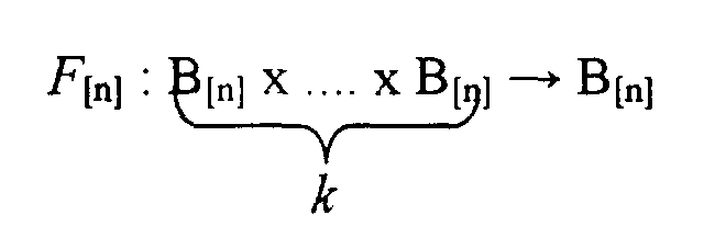
- n ⁇ ; and k ⁇ a k-ary bitvector function on bitvectors of width n is a function.
- Bitvector functions G [1] : B x ... x B ⁇ B on bitvectors of width 1 are called Boolean functions.
- n ⁇ , k ⁇ , and F [n] be a k-ary bitvector function on bitvectors of width n.
- F [n] is a bitwise bitvector function if there exists a k-ary Boolean function G [1] such that: F [n] ⁇ ( G [1] , G [1] ,... G [1] ) i.e.
- F [n] operates uniformly on all bit positions of its arguments according to G [1] . If two k-ary bitwise Boolean functions F 1 [n] and F 2 [m] , one taking bitvectors of width n as arguments and the other bitvectors of width m, operate according to the same Boolean function G [1] , then this correspondence is denoted by F 1 [n] ⁇ F 2 [m] .
- x [8] , y [8] , z [8] are bit-vector variables of width 8 and let x ' [4] , y ' [4] , z ' [4] , be bit-vector variables of width 4.
- G F 3 [8] ( x [8] , y [8] , z [8] ): ( x [8] [7,4] and y [8] [7,4]) ⁇ z [8] [3,0];
- F 3 [8] is a bitvector function, but not bit-wise.
- C be one of the equivalence classes computed by the granularity analysis.
- an equivalence class C i containing chunks of width n i .
- a ⁇ ( C i ) ⁇ n i is computed, ⁇ ( C i ) depending on the number of chunks residing in C i and on the number of possible inequalities between these chunks, as determined by the guards of if-then-else expressions in the bitvector equations.
- the satisfiability problem B [ni] which is related to C i according to method 1, is satisfiable if and only if the modified satisfiability problem B [ ⁇ (Ci)] , in which each chunk of C i is replaced by a corresponding chunk of width ⁇ (C i ) , i.e. we have B [ni] ⁇ B [ ⁇ (Ci)] , is satisfiable.
- V [ n ] ⁇ x 1 [ n ] , x 2 [ n ] , x k [ n ] ⁇ be a finite set of k bitvector variables of width n ⁇ .
- y [16] The granularity of y [16] , for example , is given by: ⁇ y [16] ⁇ 15,8>, y [16] ⁇ 7,0> ⁇ , i.e. y [16] [15,8] ⁇ y [16] [7,0]
- Method 1 and method 2 yield that the original system E of bitvector equations is satisfiable if and only if the reduced system E' , where all chunks of each class C i are reduced to a width, ⁇ (C i ) , is satisfiable.
- ⁇ ( C ) depends only on the sizes and number of the connected components of the corresponding undirected graph of C and I .
- the computation of the number of connected graph components for each class can efficiently be done by using a union-find algorithm, and, moreover, can be embedded within the computation of the equivalence classes during the granularity analysis.
- V [n] ⁇ x 1 [n] ,.., x k [n] ⁇ be a set of bitvector variables
- B [n] ( x 1 [n] ,..., x k [n] ) be a bitwise bitvector function and I ⁇ V [n] ⁇ V [n] .
- B [m] denote the corresponding bitwise bitvector function with B [m] ⁇ B [n] on bitvector variables x ' 1 [m] ,..., x ' k [m] of width m
- P ( B [m] , I ) denote the following satisfiability problem:
- each satisfiability problem belonging to an equivalence class C can be described by a bitwise bitvector function B [n] and a set of inequalities I .
- V [n] ⁇ x 1 [n] ,... , x k [n] ⁇ be a finite set of k bitvector variables of width n ⁇ .
- I ⁇ V [n]
- m max ⁇ ⁇ (V [n] , I ), 1 ⁇ .
- B [n] k-ary bitwise bitvector function
- P ( B [m] , I ) ⁇ P ( B [n] , I ) and not ( P ( B [m -1 ] , I ) ⁇ P ( B [n] , I ))
- m is the minimum width for which P ( B [m] , I ) is satisfiable if and only if P ( B [n] , I ) is satisfiable.
- the RTL unit incorporates 16 FIFO queue buffers, 810, and complex control logic, 812. Memory addresses are fed to 33 input channels to the multiplexer unit, 804, stored in FIFO's and, upon request, output from one of 17 output channels, 816, while the cell sequence is preserved and no addresses are allowed to be dropped from the management unit.
- the prototype was used as preprocessor to a collection of known property checking tools. Three different properties, nop, read and write were required to be verified, which specified the intended behaviour within a range of 4 timesteps (nop, write), respectively 6 timesteps (read). It transpired that the write property did not hold due to a design bug in the Verilog code.
- a counterexample for the reduced model was found by the property checkers and recomputed by the prototype into a counterexample for the original design, whereupon the bug was fixed by the designers and the property was again checked on the corrected design (write fail, write hold). All runtimes on the reduced models were compared to those achieved on the original design without preprocessing. The results are given in CPU seconds (respectively minutes) and are shown in Figure 9.
- the present invention provides a significant reduction in the different sizes of the design models and a tremendous drop in the runtimes of the property checkers.
- Design sizes could be reduced to approximately 30% of the original sizes, and runtimes dropped from between half and three quarters of an hour to minutes or even seconds. Note, in particular, that the computation times the prototype took to analyse the designs and generate the reduced models, ranging between 3 and 7 seconds, are negligible compared to the runtimes of the property checkers.
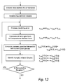
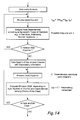
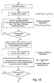
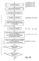
- Figures 10-18 show flow charts for granularity analysis, minimal width abstraction, model generation, together with three corresponding examples.
- the present invention provides an abstraction technique which, given a high-level circuit and a property specification, scales down the design by reducing the widths of input, output and internal signals.
- the method provides a one-to-one abstraction, which yields minimal models with respect to the minimality statement we have given. If a property fails, counterexamples for the original design can be computed from counterexamples for the reduced model. Pre- and post-processing of design and counterexample and the property checking process itself are strictly separated.
- the proposed method is independent of the system realization of the property checker and can be combined with a variety of existing verification techniques which take RTL netlists as input, no matter if the underlying prover engines operate on bit-level (like SAT or BDD-based approaches), or use high-level techniques (e.g. Integer Linear Programming, Arithmetic Constraint Solving).
- the approach is particularly well suited to SAT and BDD-based hardware verification, since the complexity of those techniques depends on the number of variables such provers have to deal with.
Abstract
Description
- The present invention relates to a method of circuit verification in digital design and in particular relates to a method of register transfer level property checking to enable the same.
- Today's electrical circuit designs frequently contain up to several million transistors and circuit designs need to be checked to ensure that circuits operate correctly. Formal methods for verification are becoming increasingly attractive since they confirm design behaviour without exhaustively simulating a design. Over the past years, bounded model checking and bounded property checking have increased in significance in electronic design automation (EDA). When checking large industrial circuits, long run times, ranging between hours and several days, are quite common. With designs continually increasing in size and complexity the test for correct behaviour becomes more important and a major economic issue, but at the same time becomes more complex, time consuming and expensive. Automated abstraction techniques have been developed to enhance capabilities of formal verification methods.
- Abstraction techniques are used as a pre-process in high-level property checking of digital circuits. The majority of today's industrial hardware verification tools use bit-level decision procedures, like decision procedures for the Boolean satisfiability problem (SAT) or decision procedures based on binary decision diagrams (BDDs). In electronic design automation, SAT procedures have many direct applications, including test pattern generation, timing analysis, logic verification, functional testing, etc. SAT belongs to the class of NP-complete problems, with algorithmic solutions having exponential worst case complexity. This problem has been widely investigated and continues to be so because efficient SAT techniques can greatly affect the operation of many EDA tools. For example in VLSI CAD, SAT formulations start from an abstract circuit description, for which a required output value needs to be validated. The resulting formulation is then mapped on to an instance of SAT. Conjunctive Normal Form (CNF) formulae can be used and several versions of this procedure incorporate a chronological backtrack-determination: at each node in the search tree, an assignment is selected and a subsequent search procedure is controlled by iterative application of "unit clauses" and "pure literal rules". Non-chronological backtrack determinations are also known. An alternative to SAT are BDDs: a set of BDD's can be constructed representing output value constraints. The conjunction of all the constraints expressed as a Boolean product of the corresponding BDD (termed as a product BDD) represents the set of all satisfying solutions. Any element of the resulting constraint set gives a feasible SAT solution. However a major limitation of this approach is that there is a corresponding exponential increase in memory requirement for the operating system and in run times of the verification tools. The CNF-based SAT solvers can be directly applied to circuits, which are broken down into bit-level Boolean logic, by transforming the entire circuit into CNF formulae. However, since practical gate-level circuit descriptions can be quite large, dealing with substantially large CNF formulae results in unacceptable CPU run times. However, circuit designs are usually defined in terms of Register-Transfer-Level (RTL) specifications, for example, coded in hardware description languages (HDL's) like VHDL or Verilog. RTL specifications of digital circuits contain explicit structural information which is lost in bit-level descriptions. At the bit-level, for example in gate lists, all signals are of 1-bit width and all available functional units are Boolean gates. In contrast, with RTL, word-level data structures, for example bit-vectors and buses, as well as high-level operators, for example adders, multipliers and shifters, are still visible. Several approaches to formal circuit verification have been proposed which make use of such high level information.
D. Cyrluk et al present a word-level decision procedure for the core theory of bit-vectors with extraction and concatenation in "An efficient decision procedure for the theory of fixed sized bit-vectors" (CAV-97), pages 60 to 71, 1997, using bit-vector BDDs and applying width abstraction to the core theory. - The present invention seeks to provide an improved circuit verification procedure.
- In accordance with a first aspect of the invention, there is provided a digital circuit design verification method wherein, prior to a property checking process for each property of a non-reduced RTL model, a reduced RTL model is determined, which reduced RTL model retains specific signal properties of a non-reduced RTL model which are to be checked.
- Conveniently the design verification process comprises, in a step prior to the determination of a reduced width RTL model, of determining the design specification of the digital circuit design and the specification of the properties to be investigated, synthesising an RTL netlist of high level primitives whereby the circuit is defined as an interconnection of control and data path portions, wherein in signals of a width n are determined such that:wherein bitvectors of respective length determine the signal value. Conveniently, in the property checking process, an internal bit level representation contains a bit level variable for each bit of each word signal. This bit-level representation is passed to a verification engine and then to a property test unit which operates to provide a positive result if the investigated property holds true for the circuit and which operates to provide a counter-example if the property does not hold. In the event that a counter-example is produced for the reduced RTL design, signal width enhancement is performed to create a counter-example for the original RTL.
- In accordance with a further aspect of the present invention there is provided a digital circuit design verification tool wherein a pre-property checking unit is operable to reduce the widths of the signals occurring in an RTL model of an input design specification and an input property specification, which reduced width RTL model retains the specific signal property of a non-reduced RTL model.
- Preferably the tool further comprises a front end unit operable to receive input data relating to a design specification and the property characteristics of a design to be verified and is operable to provide an RTL netlist of the circuit design and property whereby the circuit can be defined as an interconnection of control and data path portions, wherein in signals of a width n are determined such that
n ∈; and bitvectors of a respective length determine the signal value. Conveniently a property checking unit is operable to create an internal bit level representation having received a reduced RTL representation. This representation is sequentially passed to a verification engine and to a property test unit. The property test unit being operable to provide a positive result if the circuit property holds true and which is operable to provide a counter-example in the case of the property does not hold. Conveniently the signal width enhancement unit is operable to receive counter-examples for reduced RTL data and to expand the signal width to provide a counter example for the original RTL.
- A linear signal width reduction causes an exponential reduction of the induced state space. Reducing state space sizes in general goes hand in hand with reduced verification runtimes. Thus the technique holds a high potential for speeding up verification tasks. Tests have shown that the present invention can significantly reduce the runtimes of existing prover tools. Furthermore, the present invention will be able to process design sizes which have, hitherto, exceeded the capacities of existing verification tools and which could not be taken into account before due to resource limitations. FIFO's, queues, stacks, bridges and interface protocols comprise part of a class of digital hardware designs to which the present invention is particularly well suited to processing.
- A further advantage of the present invention is that, if the analysis yields that no reduction at all is possible for a given design and a given property, then reduced model and original design are identical. The verification task itself cannot be impaired by using the proposed method as a pre-process, and in all case studies pre-processing runtimes were negligible Furthermore, the technique can be applied in high-level equivalence checking and high-level simulation. High-level equivalence checking, for example, can be considered a special case of high-level property checking. The design specification can include two different implementations of the same circuit and the property can require functional equivalence, or the property itself can be written in a hardware description language representing a functional specification of the circuit.
- The invention may be understood more readily, and various other aspects and features of the invention may become apparent, from consideration of the following description and the figures as shown in the accompanying drawing sheets, wherein:
- Figures 1a and 1b show property checking flow diagrams;
- Figure 2 shows the basic steps involved in the abstraction technique of this invention;
- Figure 3 is a table detailing the syntax of various bit-vector operators supported in the reduction technique of this invention;
- Figure 4 is a flow chart detailing the generation of the reduced RTL model;
- Figure 5 shows the effect of slicing equivalence classes;
- Figure 6 illustrates a granularity analysis in terms of bit-vectors, dependency classes of bit-vector chunks and granularities; and
- Figure 6a details a process for determining the granularity analysis of bit-vector equations;
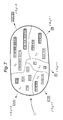
- Figure 7 illustrates a minimum width computation for a dependency class;
- Figure 7a details a process for reduced model generation;
- Figure 8 shows a block diagram of an Asynchronous Transfer Mode (ATM) switching element operable in accordance with the invention;
- Figure 9 comprises tabulated results of the address management unit shown in Figure 8;
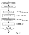
- Figure 10 shows a granularity analysis flow chart together with a first example;
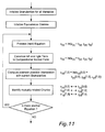
- Figure 11 shows a granularity analysis flow chart together with a second example;
- Figure 12 shows a granularity analysis flow chart together with a third example;
- Figure 13 shows a minimal width abstraction flow chart together with a first example;
- Figure 14 shows a minimal width abstraction flow chart together with a second example;
- Figure 15 shows a minimal width abstraction flow chart together with a third example;
- Figure 16 shows a model generation flow chart together with a first example;
- Figure 17 shows a model generation flow chart together with a second example; and
- Figure 18 shows a model generation flow chart together with a third example.
-
- There will now be described by way of example, the best mode contemplated by the inventor for carrying out the invention. In the following description numerous specific details are set out in order to provide a complete understanding of the invention. It will be apparent however, to those skilled in the art, that the present invention may be put in to practice with variations of the specific.
- Referring to Figure 1a there is shown a prior-art property checking flow diagram. A property specification, 112, and a design specification, 114, is presented to a bounded property checker, 120. The property and design specifications, 112, 114, are input to a front end processor which converts the specifications to Register Transfer Level (RTL) specifications. A decision relating to the property is made at decision point 122: if the property holds then the design feature is confirmed 124; if the property does not hold, then a counterexample 126 is determined. A counterexample, as is known, is an indication that a circuit does not function in the way intended by the designer; a counterexample is given in terms of assignments of values to the circuit inputs such that a violation of the desired behaviour which is described by the property specification can be observed when looking a the values of the circuit outputs resulting from the circuit inputs. A design modification would be made to eliminate the occurrence of the counterexample and, indeed, further counterexamples which may consequentially arise.
- The present invention employs the use of properties described in a linear time logic over finite bounded intervals of time. Properties consist of an assumption part which implies a commitment part:
- Properties specify the intended behaviour of the design within a finite interval of time and consist of temporal operators and state expressions, involving relationships among data words. As an example consider:
- assume (during [t+0, t+4]: reset = 0) and (at t+0: request = 1);
- prove (at t+3: acknowledge = 1) and (at t+4: data = 11111111);
-
- Referring now to Figure 1b, there is shown a property-checking flow in accordance with the invention. As a first step, design and property are synthesized into a flattened netlist of high-level primitives, called an RTL netlist, as is known. These netlists include word-level signals, word-level gates, arithmetic units, comparators (data to control), multiplexors (control to data) and memory elements Each signal x has a fixed given width nand takes bitvectors of respective length as values. The RTL representation of the design is handed to a property checker which translates the netlist into a bit-level representation and either proves that the property holds for the given design, or returns a counterexample.

- In a pre-processing step prior to the invocation of the property checker, the RTL netlist is obtained, 118, and a scaled down RTL model 130 is computed by signal-width reduction processor, 128, in which signal widths are reduced, while guaranteeing that:
- The reduced RTL, 130, is given to the property checker, 132, instead of the original RTL. The internal bit-level representation, 138, used by the property checker contains a bit-level variable for each bit of each word-level signal of the RTL representation, and, depending on the degree of reduction of the signal widths, now can contain significantly less variables for the reduced RTL. The property checker, 132 includes a verification engine (SAT, BDD...), 140. If the property does not hold, the property checker returns a counterexample in terms of an assignment of values to all inputs of the reduced RTL, 134. The method provides a technique which takes such counterexample and generates an assignment of values to the inputs of the original design in a signal width enhancement step by signal width enhancement processor, 136, such that the property does not hold when these input values are applied to the circuit, and provides a counterexample, 126.
- The invention conveniently uses structural data-path dependency analyses for minimum width abstractions. The basic idea is illustrated by the following introductory examples.
- In a first example, example 1, we assume we want to check if the conjunction of two word-level signals of width 8, denoted by x [8] and y [8] can evaluate to the 8-bit zero vector. Let 'and' denote bitwise Boolean conjunction. In RTL, we have to check if the equation
- In the example above, signals x [8] and y [8] both could be reduced to a width of one bit. In general, reduction depends on the structural data dependencies occurring in the cone of influence of a signal in a given design.
- In a second example, given the assumptions of Example 1, we let z [4] be an additional word-level signal of width 4 and assume that z [4] is assigned to the 4 most significant bits of x [8]. That is to say we have to check if the following system of equations is satisfiable:
- System (3) is satisfiable if and only if (4) is satisfiable. To obtain a solution of (3), we copy x '[2][1, 1] into all positions of x [8] [7, 4] and x '[2] [0, 0] into all positions of x [8] [3, 0]. The same is done for y '[2] and y [8], and z '[1] is copied into all positions of z [4]. For example, x '[2] = 10, y '[2] = 01, z '[1] = 1, yields x [8] = 11110000, y [8] = 00001111 and z [4] = 1111.
- Signals x [8] and y [8] are both split into two parts, and each part can be reduced to a width of one bit, resulting in an overall width of 2 bits for x '[2] and y '[2]. In general, it is not always possible to reduce a chunk of bits processed in exactly the same manner to only one bit. Equations containing dynamic data dependencies, e.g. if-then-else operators, require an analysis of all possible inequalities between signals, as shown in the following example.
- In a third example, we let x [8], y [8] and z [8] be data signals of width 8, and let a [1], b [1] and c [1] be control signals. The satisfiability of the following system of equations can be characterised as:Obviously, x [8], y [8] and z [8] cannot be reduced to a width of only one bit, because x [8]≠ y [8] ∧ y [8] ≠ z [8] ∧ z [8] ≠ x [8] is satisfiable, while x '[1] ≠ y '[1] ∧ y '[1] ≠ z '[1] ∧ z '[1] ≠ x '[1] is not. Insted the following holds:
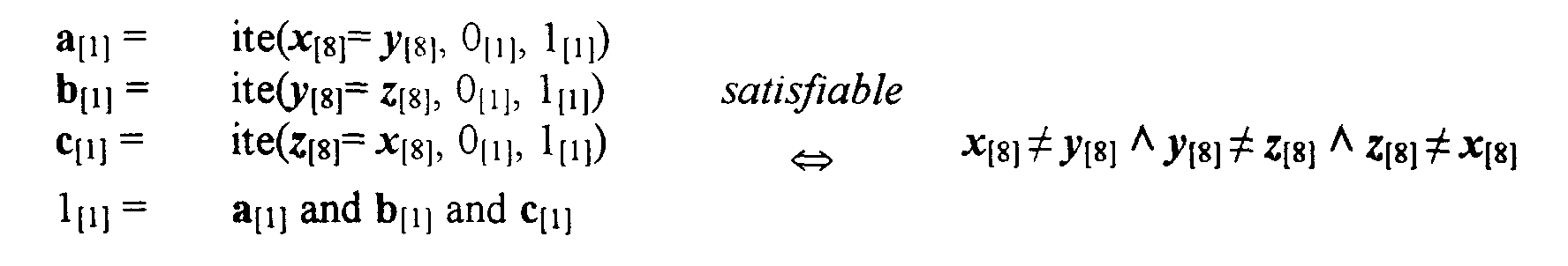
Instead, the following holds:is true, and thus the original system of equations can be replaced by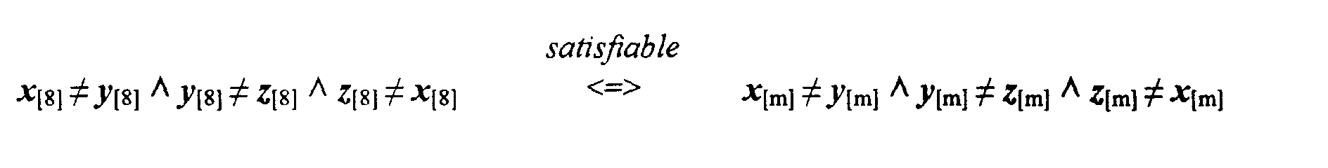
- a '[1] = ite( x '[2]= y '[2], 0[1], 1 [1])
- b '[1] = ite( y '[2]= z '[2], 0[1], 1 [1])
- c '[1] = ite( z '[2]= x '[2], 0[1], 1 [1])
- 1[1] = a '[1] and b '[1] and c '[1] Without changing satisfiability.
-
- The process of scaling down signal widths is separated into two sequential phases.
- The basic idea of this abstraction technique is shown in the flow chart, 200, of Figure 2, as will be described below. First, the coarsest granularity of each word-level signal x [16] is computed, as determined by the structural data dependencies in a granularity analysis step, 210. A granularity is a separation of a signal into several contiguous chunks, 218, which indicate the coarsest possible subsumptions of individual bits of the signal, which are treated in the exact same manner with respect to structural data dependencies. Then, for each chunk, the necessary minimum width, 220, is computed, as required by dynamical data dependencies in a minimum width abstraction step, 212. According to these computed minimum chunk widths, the reduced width for the corresponding variable is reassembled, in a reduced model generation step, 214, to be provide a reduced signal, 222.
- The present invention provides an equational theory BVext of fixed-size bitvectors, derived from the core theory of bitvectors. Let B = {0, 1} denote the set of bit values 0 and 1. A bitvector of width n ∈is a vector element of B n , consisting of n individual bits which are indexed from right to left, starting with index 0. Bitvectors are written as binary bitstrings, and, accordingly, the set B n of bitvectors of length n is denoted by B[n]. The invention provides a bitvector variable definition wherein, for n ∈
 , a bitvector variable x [n] of width n is a typed variable, representing fixed-size bitvectors v ∈ B[n] of width n.
- Fixed-size in this context means that for each bitvector variable the width n is a fixed (but arbitrary) positive natural number. We write x [n][i] to refer to the i th bit of x [n]. BV ext includes bitvector variables and bitvector constants c [n], n ∈and c ∈ B[n]. The present invention, compared to the core theory of bitvectors, provides additional high-level operators as tabulated in Figure 3. Further operators, like shifts, rotations or further comparisons, are conveniently expressed within this theory. The Boolean predicates = and < occurring in the guards of ite (if-then-else) expressions, are defined on two bitvector arguments of equal width. Equality is defined bitwise, whereas < is defined according to the lexicographical order of bitstrings.

- The set of terms is defined over a set of free bitvector variables and the operators shown in Figure 3. If the terms are "well-formed" then the terms require variable widths to comply with operator demands, and index expressions must not exceed the widths of argument terms. A valuation is an assignment of values to the bitvector variables occurring in the terms. A system E of equations over such terms is satisfiable if there exists a valuation of the variables such that all equations of E hold simultaneously. Correspondingly, we define the term "valid" such that E is universally valid if all possible valuations satisfy E.
In a fourth example, x [16] y [4] and z [4] are bitvector variables. Consider: - 1. x [16][15,8] ⊗ x [16] [7,0] = x [16]
- 2. x [16] = neg ( x 16])
- 3. y [4] and 1100[4] = z [4] Equation 1 is universally valid and Equation 2 is unsatisfiable. Equation 3 is satisfiable, e.g. by y [4] := 0111[4] and z [4] := 0100[4], but not universally valid.
-
- Consider the system of equations given above. Taken separately, the first and second equations are satisfiable. However, the system of equations, as a whole, is unsatisfiable.
- Referring now to Figure 4, there is illustrated the steps of the proposed abstraction technique in accordance with the present invention. As a first step, the RTL representation of design, 410, and property is translated into a system E, 412, of equations of bitvector terms over BVext, such that:
- A possible solution of E, if existent, would be a counterexample which would give value assignments to all circuit signals, such that the property does not hold for these assignments.
- The data dependencies within the bitvector equations of E are analysed, 414, and a second system E', 416, of bitvector equations is computed, in which the type (i.e. the width) of each bitvector variable is reduced to a smallest number of bits that is possible with respect to the abstraction technique, such that:
- E' is translated back to an RTL netlist, 418, representing a scaled down version of the original design. According to (7), the property checking task can be completely carried out on the reduced model.
- Given a system E of bitvector equations over BV ext, structural and functional dependencies are imposed on the bitvector variables by the high-level operators occurring in the equations. Dependencies may be found between complete variables or only between certain parts. For each variable, the present invention analyses such dependencies and determines the contiguous parts in which all bits are treated uniformly with respect to data dependencies.
- Further definitions are now provided for 'Chunk' and 'Granularity': A chunk x [-n]<j,i>, o ≤ i ≤ j < n, of a bitvector variable x [n] is a syntactical representation for a contiguous part of x [n], i.e. x [n] <j,i> := x [n] [j,i].
- Chunks are used to describe the above-mentioned contiguous parts of bitvector variables.
- A granularity of a bitvector variable x [n] is any ordered decomposition of x [n] into chunks { x [ n ]<j2 ,i1>, x [n] <jq ,i q>} 0 = i1<j1 = 1 = i2 < j 2 +1 = ... = i q < j q + 1 = n, such that
- In a sixth example, x [16] is a bitvector variable. { x [16]<15,18>, x [16]<7,4>, x [16]<3,0>} is a granularity of x [16], whereas { x [16]<15,10>, x [16]<5,0>} and { x [16]<15,5>, x [16]<10,0>} is not.
- Granularities are used to describe how different data dependencies exist for different chunks of a bitvector variable. Non-uniform structural dependencies occur whenever a variable (or a term) is not treated as a whole, but separated into parts upon which different operations are performed, e.g. by extractions or concatenations.
- The relation between granularities and structural dependencies is shown in a further example: consider the following bitvector equation:
- The concatenation on the right hand side of the equation imposes different dependencies on the upper and lower part of x [8], the first depending on y [4], the latter on z [4]. This is described by the granularity { x [8](7,4), x [8] (3,0)}.
- For each bitvector variable x [n], the method in accordance with one aspect of the invention computes the coarsest possible granularity which describes the splitting of data dependencies for x [n], as imposed by the equations of E. Slicing is performed only if necessary. For example, the equation x [16] = y [16] [15,12] ⊗ y [16][11,0] is equivalent to x [16] = y [16] and does not require slicing of x [16]. Hence, initially a normalization of all bitvector terms is performed. The computation of the coarsest granularities is carried out using an equivalence class structure which groups chunks between which functional dependencies are detected.
- Granularity analysis and functional dependencies are shown in another example. The equation given in the fourth example imposes functional dependencies between x [8][7,4] and y [4][3,0] and between x [8][3,0] and z [4][3,0]. The resulting equivalence classes are { x [8]<7,4>, y [4]<3,0>} and { x [8]<3,0>, z [4]<3,0>}. As a second example consider x [16] = y [16] or z [16]. Here, x [16], y [16] and z [16] are related to each other by a bitwise Boolean operator, requiring that all three go into the same equivalence class { x [16]<15,0>, y [16]<15,0>, z [16]<15,0>}.
- The equivalence class computation works incrementally and can efficiently be performed by employing a union-find algorithm, which, besides the known union() and find() operations, defines a new procedure slice(). Initially, in each bitvector group of classes, 510, variable x [n] resides in its own singleton equivalence class: { x [n]<n - 1,0>}. Find ( x [n],i) yields the (non ambiguous) equivalence class, which includes a chunk of x [n]which contains bit position i, union() performs the usual set union of two classes, and slice( x [n],j,i) calls find( x [n],i) and find( x [n],j) and splits all chunks of the respective classes at the bit positions corresponding to i and j and groups the originating parts in two new equivalence classes, as illustrated in Figure 5, with a second group of classes, 512.
- Figure 6 exemplifies a granularity analysis in terms of bitvectors, dependency classes of bitvectors chunks and granularities. Each bitvector equation e is processed sequentially by the analyser and the next state of the equivalence class structure is computed by means of the procedure gran(e), which is outlined in process 1 as shown in Figure 6a. Once all bitvector equations have been processed, for each bitvector variable the coarsest possible granularity is given by the state of the equivalence classes.
- The granularity analysis decomposes the initial satisfiability problem for E into a number of independent satisfiability problems, characterized by the computed equivalence classes. The solutions of these problems can be characterized by bitwise bitvector functions, as will be defined as follows:
- Let n ∈; and k ∈
 , a k-ary bitvector function on bitvectors of width n is a function.
- Bitvector functions G [1] : B x ... x B → B on bitvectors of width 1 are called Boolean functions.
Let n ∈, k ∈ , and F [n] be a k-ary bitvector function on bitvectors of width n. F [n] is a bitwise bitvector function if there exists a k-ary Boolean function G [1] such that:
in a ninth example x [8], y [8], z [8] are bit-vector variables of width 8 and let x '[4], y '[4] , z '[4], be bit-vector variables of width 4. Let
Let C be one of the equivalence classes computed by the granularity analysis. The set of all satisfying solutions of E, projected to the chunks contained in C, can be characterized by a first theorem with respect to satisfiability:
If C = { x 1 [ n 1] <j 1, i 1 >,..., xk [n]<jk , ik > },
with j 1 - i 1 = ...=jk - ik = n, then there exists a k-ary bit-wise bit-vector function: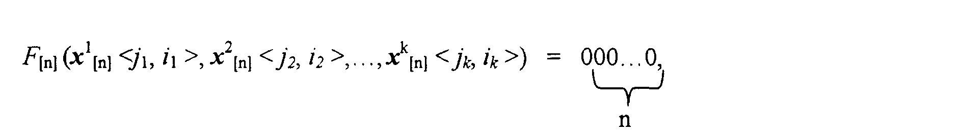
- Referring now to Figure 7, there is shown an equivalence class Ci containing chunks of width ni . For each such class Ci , a ϕ(Ci ) ≤ ni is computed, ϕ (Ci ) depending on the number of chunks residing in Ci and on the number of possible inequalities between these chunks, as determined by the guards of if-then-else expressions in the bitvector equations.
- The satisfiability problem B [ni] , which is related to Ci according to method 1, is satisfiable if and only if the modified satisfiability problem B [ϕ(Ci)] , in which each chunk of Ci is replaced by a corresponding chunk of width ϕ(Ci), i.e. we have B [ni] ≃ B [ϕ(Ci)] , is satisfiable. We will now consider the reduction of bitvector widths with a second method: Let V [ n ] = { x 1 [ n ], x 2 [ n ], xk [ n ]} be a finite set of k bitvector variables of width n ∈
- The information about possible inequalities is obtained during the Granularity Analysis and annotated within the equivalence classes. For each equivalence class C we define ϕ(C) := max{ϕ(V[n] , I ),1}, where V[n] is the set of chunks in C, and I is the set of possible inequalities annotated to C. The reduced system E' of bitvectors equations is constructed according to process 2.
- Example 10. Let x [8], y [16], z [16] be bitvector variables and assume that E contains the following equation:
- Assume that granularity analysis and minimum width abstraction yield the following results:
- The granularity of y [16], for example, is given by:
- According to the minimum chunk widths, the corresponding reduced variable is assembled as follows:
- Hence, the reduced equation of E', which corresponds to (8) of E is:
- Indices of extraction expressions are modified according to the new chunk widths.
- Method 1 and method 2 yield that the original system E of bitvector equations is satisfiable if and only if the reduced system E', where all chunks of each class Ci are reduced to a width, ϕ(Ci), is satisfiable.
- Accordingly a third method is applied: The reduced system E' of bitvector equations which results from the proposed abstraction technique is satisfiable if and only if the original equational system E is satisfiable. For each solution of the reduced system a solution of the original system can be computed.
- It is to be understood that ϕ(C) depends only on the sizes and number of the connected components of the corresponding undirected graph of C and I. The computation of the number of connected graph components for each class can efficiently be done by using a union-find algorithm, and, moreover, can be embedded within the computation of the equivalence classes during the granularity analysis.
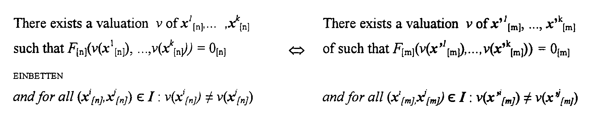
- Let V[n] = { x 1 [n] ,.., x k [n] } be a set of bitvector variables, B [n] ( x 1 [n],..., x k [n] ) be a bitwise bitvector function and I ⊆ V[n] × V[n] . For m ∈, let B [m] denote the corresponding bitwise bitvector function with B [m] ≃ B [n] on bitvector variables x ' 1 [m],..., x 'k [m] of width m, and let P( B [m] , I ) denote the following satisfiability problem:

- There exists a valuation v of x 1 [m],..., x k [m] such that:
-
- According to Theorem 1, each satisfiability problem belonging to an equivalence class C can be described by a bitwise bitvector function B [n] and a set of inequalities I . The reduced chunk width m := ϕ(C) computed in Theorem 2 is independent of any further mathematical property of B [n] , i.e. we purposely abstract from the concrete aspects of B [n] except for bitwise operation. m is minimal with respect to this abstraction, which leads to a fourth theorem, relating to minimality:.
- Let V[n] = { x 1 [n],... , x k [n]} be a finite set of k bitvector variables of width n ∈. Let I ⊆ V[n], and let m := max{ ϕ(V[n], I), 1}. Then there exists a k-ary bitwise bitvector function B [n]( x 1 [n],..., x k [n]) such that

- A prototype system was implemented in C++ and tested in several case studies at the Design Automation department of Siemens Corporation in Munich and at the Computer Network Peripherals department of Infineon Technologies in San Jose, CA. All test cases were run on an Intel Pentium II PC with a 450 MHz CPU, 128 MB main memory and a Linux operating system. Referring to Figure 8, which shows a block diagram of an ATM switching element 800, a case study of an address management unit of an ATM switching element will now be discussed. Results are tabulated in Figure 9. The design comprised of approximately 3000 lines of Verilog code, the netlist synthesis comprised of approximately 24.000 gates and 35.000 RAM cells. Signals input to cell inputs 802, which are multiplexed by multiplexer, 804, to a central RAM, 814, or via a target decoder 806 to an RTL unit 808, which provides signals to the central RAM. The RTL unit incorporates 16 FIFO queue buffers, 810, and complex control logic, 812. Memory addresses are fed to 33 input channels to the multiplexer unit, 804, stored in FIFO's and, upon request, output from one of 17 output channels, 816, while the cell sequence is preserved and no addresses are allowed to be dropped from the management unit.
- The prototype was used as preprocessor to a collection of known property checking tools. Three different properties, nop, read and write were required to be verified, which specified the intended behaviour within a range of 4 timesteps (nop, write), respectively 6 timesteps (read). It transpired that the write property did not hold due to a design bug in the Verilog code. A counterexample for the reduced model was found by the property checkers and recomputed by the prototype into a counterexample for the original design, whereupon the bug was fixed by the designers and the property was again checked on the corrected design (write fail, write hold). All runtimes on the reduced models were compared to those achieved on the original design without preprocessing. The results are given in CPU seconds (respectively minutes) and are shown in Figure 9.
- The present invention provides a significant reduction in the different sizes of the design models and a tremendous drop in the runtimes of the property checkers. Design sizes could be reduced to approximately 30% of the original sizes, and runtimes dropped from between half and three quarters of an hour to minutes or even seconds. Note, in particular, that the computation times the prototype took to analyse the designs and generate the reduced models, ranging between 3 and 7 seconds, are negligible compared to the runtimes of the property checkers.
- Figures 10-18 show flow charts for granularity analysis, minimal width abstraction, model generation, together with three corresponding examples.
- Reduced runtimes and a reduced requirement for memory needed in computations is one requirement to match today's sizes of designs in hardware verification. The present invention provides an abstraction technique which, given a high-level circuit and a property specification, scales down the design by reducing the widths of input, output and internal signals. The method provides a one-to-one abstraction, which yields minimal models with respect to the minimality statement we have given. If a property fails, counterexamples for the original design can be computed from counterexamples for the reduced model. Pre- and post-processing of design and counterexample and the property checking process itself are strictly separated. The proposed method is independent of the system realization of the property checker and can be combined with a variety of existing verification techniques which take RTL netlists as input, no matter if the underlying prover engines operate on bit-level (like SAT or BDD-based approaches), or use high-level techniques (e.g. Integer Linear Programming, Arithmetic Constraint Solving). The approach is particularly well suited to SAT and BDD-based hardware verification, since the complexity of those techniques depends on the number of variables such provers have to deal with.
- In known SAT and BDD-based circuit verification such variables are created (at least) for each single bit of each signal of the circuit. In Bounded Property Checking even multiple instances of each variable and each signal have to be created for each step of the considered interval of time. In practice, design sizes range from several thousands up to 2 - 5 million gates and typical bounded properties incorporate 2 - 30 timesteps depending on the field of application.

A satisfying solution for the original system can be obtained from a solution of (5) by a sign extension of the values of the reduced variables, e.gof the reduced variables, e.g., x '[2] = 00, y '[2] = 01, z '[2] = 10, yields x [8] = 00000000, y [8] = 00000001 and z [4] = 11111110.
In a fifth example x [8] and y [4] are bitvector variables.
Claims (13)
- A digital circuit design verification method characterised in that for each property of a non reduced RTL model a reduced RTL model is determined for a design specification, which reduced RTL model retains the signal property of the non-reduced RTL model and which reduced RTL model is subjected to a property checking process.
- A digital circuit design verification method in accordance with claim 1, wherein prior to the determination of a reduced width RTL model, the design specification and properties of a digital circuit design are determined; and,
an RTL netlist of high level primitives is synthesised whereby the circuit is defined as an interconnection of control and data path portions, wherein signals of a width n are determined such that n ∈;
and bitvectors of respective length determine the signal value. - A digital circuit design verification method in accordance with claim 1 or 2 wherein in the property checking process, an internal bit-level representation contains a bit-level variable for each bit of each word signal, which representation is sequentially passed to a verification engine and then to a property test unit which operates to provide a positive result if the circuit property holds true and which operates to provide a counterexample in the case that the property does not hold.
- A digital circuit design verification method in accordance with claim 3 wherein, in the event that a counterexample is produced for the reduced RTL design, signal width enhancement is performed to create a counterexample for the original RTL.
- A digital circuit design verification method in accordance with claim 1, wherein the RTL model includes word-level signals comprising bit-vectors and, for each bit-vector variable, the method of reducing the RTL model is separated into two sequential steps;the first step comprising the computation of the coarsest granularity of each word-level signal whereby to separate each signal into several contiguous chunks which indicate the basic groups of bits with respect to structural data dependencies,the second step comprising the computation of the minimum width with respect to dynamic data dependencies.
- A digital circuit design verification method in accordance with claim 5,
wherein, for each bit-vector variable, the computation of coarse granularities is performed by means of an equivalence class structure,
whereby an initial satisfiability problem can be considered as a number of independent satisfiability problems. - A digital circuit design verification method in accordance with claim 6, wherein the solution of the independent satisfiability problems can be determined by bit wise bit-vector functions.
- A digital circuit design verification tool characterised in that a pre-property checking unit is operable to reduce the widths of the signals occurring in an RTL model of an input design specification, which reduced width RTL model retains the signal properties of a non reduced width RTL model.
- A digital circuit design verification tool according to claim 5 wherein the tool further comprises a front end unit operable to receive input data relating to a design specification and property characteristics of a design to be verified and is operable to provide an RTL netlist of the said design and property whereby the circuit can be defined as an interconnection of control and data path portions, wherein signals of a width n are determined such that:
n ∈; and
bitvectors of respective length determine the signal value. - A digital circuit design verification tool in accordance with claim 8 or 9 wherein the property checking unit is operable to receive a reduced RTL representation and to create an internal bit-level representation containing one bit wfor each bit of each word signal, which representation is sequentially passed to a verification engine and to a property test unit, the property test unit being operable to provide a positive result if the circuit property holds true and which operates to provide a counterexample in the case that the property does not hold.
- A digital circuit design verification tool in accordance with claim 10 wherein in a signal width enhancement unit is operable to receive a counterexample for reduced RTL data and to expand the signal width to provide a counterexample for the original RTL.
- A digital circuit design verification tool in accordance with claim 8, wherein the RTL model includes word-level signals comprising bit-vectors and, for each bit-vector variable, the tool is operable to reduce the RTL model width of a signal in two sequential steps;
wherein, a first step, a coarse granularisation of each word-level signal is determined whereby to separate each signal into several contiguous chunks which indicate the basic groups of bits with respect to structural data dependencies; and,
in a second step, a minimum width with respect to dynamic data dependencies is determined. - A digital circuit design verification tool in accordance with claim 12 wherein the tool is operable to arrange coarse granularities in terms of an equivalence class structure.
whereby an initial satisfiability problem can be considered as a number of independent satisfiability problems.
Priority Applications (1)
| Application Number | Priority Date | Filing Date | Title |
|---|---|---|---|
| US10/038,870 US6728939B2 (en) | 2001-01-08 | 2002-01-08 | Method of circuit verification in digital design |
Applications Claiming Priority (2)
| Application Number | Priority Date | Filing Date | Title |
|---|---|---|---|
| DE10100433 | 2001-01-08 | ||
| DE10100433 | 2001-01-08 |
Publications (3)
| Publication Number | Publication Date |
|---|---|
| EP1221663A2 true EP1221663A2 (en) | 2002-07-10 |
| EP1221663A3 EP1221663A3 (en) | 2006-04-05 |
| EP1221663B1 EP1221663B1 (en) | 2009-06-24 |
Family
ID=7669908
Family Applications (1)
| Application Number | Title | Priority Date | Filing Date |
|---|---|---|---|
| EP01108653A Expired - Lifetime EP1221663B1 (en) | 2001-01-08 | 2001-04-05 | A method of circuit verification in digital design |
Country Status (2)
| Country | Link |
|---|---|
| EP (1) | EP1221663B1 (en) |
| DE (1) | DE60139063D1 (en) |
Cited By (2)
| Publication number | Priority date | Publication date | Assignee | Title |
|---|---|---|---|---|
| US8813019B1 (en) | 2013-04-30 | 2014-08-19 | Nvidia Corporation | Optimized design verification of an electronic circuit |
| CN113076622A (en) * | 2021-02-22 | 2021-07-06 | 南京远思智能科技有限公司 | System and method for normative analysis and verification of FMU (functional modeling Unit) simulation model |
Families Citing this family (1)
| Publication number | Priority date | Publication date | Assignee | Title |
|---|---|---|---|---|
| US8726205B1 (en) | 2013-04-15 | 2014-05-13 | Nvidia Corporation | Optimized simulation technique for design verification of an electronic circuit |
Citations (2)
| Publication number | Priority date | Publication date | Assignee | Title |
|---|---|---|---|---|
| US5465216A (en) * | 1993-06-02 | 1995-11-07 | Intel Corporation | Automatic design verification |
| US5926622A (en) * | 1997-03-18 | 1999-07-20 | Lucent Technologies Inc. | Efficient regression verification |
-
2001
- 2001-04-05 DE DE60139063T patent/DE60139063D1/en not_active Expired - Lifetime
- 2001-04-05 EP EP01108653A patent/EP1221663B1/en not_active Expired - Lifetime
Patent Citations (2)
| Publication number | Priority date | Publication date | Assignee | Title |
|---|---|---|---|---|
| US5465216A (en) * | 1993-06-02 | 1995-11-07 | Intel Corporation | Automatic design verification |
| US5926622A (en) * | 1997-03-18 | 1999-07-20 | Lucent Technologies Inc. | Efficient regression verification |
Non-Patent Citations (3)
| Title |
|---|
| HUANG CHUNG-YANG ET AL: "Assertion checking by combined word-level ATPG and modular arithmetic constraint-solving techniques" PROC DES AUTOM CONF; PROCEEDINGS - DESIGN AUTOMATION CONFERENCE 2000 IEEE, PISCATAWAY, NJ, USA, 2000, pages 118-123, XP002365707 * |
| KAVVADIAS D ET AL: "The inverse satisfiability problem" SIAM JOURNAL ON COMPUTING SIAM USA, vol. 28, no. 1, 1998, pages 152-163, XP008059300 ISSN: 0097-5397 * |
| WONG W: "Modelling bit vectors in HOL: the word library" HIGHER ORDER LOGIC THEOREM PROVING AND ITS APPLICATIONS. 6TH INTERNATIONAL WORKSHOP, HUG '93 PROCEEDINGS SPRINGER-VERLAG BERLIN, GERMANY, 1994, pages 372-384, XP008059297 ISBN: 3-540-57826-9 * |
Cited By (3)
| Publication number | Priority date | Publication date | Assignee | Title |
|---|---|---|---|---|
| US8813019B1 (en) | 2013-04-30 | 2014-08-19 | Nvidia Corporation | Optimized design verification of an electronic circuit |
| CN113076622A (en) * | 2021-02-22 | 2021-07-06 | 南京远思智能科技有限公司 | System and method for normative analysis and verification of FMU (functional modeling Unit) simulation model |
| CN113076622B (en) * | 2021-02-22 | 2023-12-12 | 南京远思智能科技有限公司 | FMU simulation model normalization analysis and verification system and method |
Also Published As
| Publication number | Publication date |
|---|---|
| DE60139063D1 (en) | 2009-08-06 |
| EP1221663B1 (en) | 2009-06-24 |
| EP1221663A3 (en) | 2006-04-05 |
Similar Documents
| Publication | Publication Date | Title |
|---|---|---|
| US6728939B2 (en) | Method of circuit verification in digital design | |
| Huang et al. | Formal equivalence checking and design debugging | |
| Rushton | VHDL for logic synthesis | |
| TWI424327B (en) | Method and apparatus for processing a computer implemented representation of a circuit design, data processing system and article of manufacture providing software adapted to the same | |
| Bloem et al. | Efficient decision procedures for model checking of linear time logic properties | |
| US6148436A (en) | System and method for automatic generation of gate-level descriptions from table-based descriptions for electronic design automation | |
| US20060150043A1 (en) | Method for clock synchronization validation in integrated circuit design | |
| US8255848B2 (en) | Logic design verification techniques for liveness checking with retiming | |
| KR100329896B1 (en) | Toggle based application specific core methodology | |
| US7856609B2 (en) | Using constraints in design verification | |
| US7882483B2 (en) | Method for checking constraints equivalence of an integrated circuit design | |
| US20050160392A1 (en) | System & method for asynchronous logic synthesis from high-level synchronous descriptions | |
| Lee et al. | Unbounded scalable verification based on approximate property-directed reachability and datapath abstraction | |
| US20080201671A1 (en) | Method for generating timing exceptions | |
| US6131080A (en) | Method of monitoring a computer simulation of an electrical circuit | |
| Benini et al. | Automatic synthesis of large telescopic units based on near-minimum timed supersetting | |
| US7257786B1 (en) | Method and apparatus for solving constraints | |
| EP1221663B1 (en) | A method of circuit verification in digital design | |
| Fujita | Equivalence checking between behavioral and RTL descriptions with virtual controllers and datapaths | |
| Ranjan et al. | Using combinational verification for sequential circuits | |
| US20090044033A1 (en) | Method for computing power savings and determining the preferred clock gating circuit of an integrated circuit design | |
| Johannsen et al. | Formal verification on the RT level computing one-to-one design abstractions by signal width reduction | |
| Clarke et al. | Abstract BDDs: a technique for using abstraction in model checking | |
| Johannsen | BOOSTER: Speeding up RTL property checking of digital designs by word-level abstraction | |
| Bombieri et al. | Automatic synthesis of OSCI TLM-2.0 models into RTL bus-based IPs |
Legal Events
| Date | Code | Title | Description |
|---|---|---|---|
| PUAI | Public reference made under article 153(3) epc to a published international application that has entered the european phase |
Free format text: ORIGINAL CODE: 0009012 |
|
| AK | Designated contracting states |
Kind code of ref document: A2 Designated state(s): AT BE CH CY DE DK ES FI FR GB GR IE IT LI LU MC NL PT SE TR |
|
| AX | Request for extension of the european patent |
Free format text: AL;LT;LV;MK;RO;SI |
|
| RAP1 | Party data changed (applicant data changed or rights of an application transferred) |
Owner name: INFINEON TECHNOLOGIES AG |
|
| RAP1 | Party data changed (applicant data changed or rights of an application transferred) |
Owner name: ONESPIN SOLUTIONS GMBH |
|
| PUAL | Search report despatched |
Free format text: ORIGINAL CODE: 0009013 |
|
| AK | Designated contracting states |
Kind code of ref document: A3 Designated state(s): AT BE CH CY DE DK ES FI FR GB GR IE IT LI LU MC NL PT SE TR |
|
| AX | Request for extension of the european patent |
Extension state: AL LT LV MK RO SI |
|
| 17P | Request for examination filed |
Effective date: 20060512 |
|
| AKX | Designation fees paid |
Designated state(s): DE FR GB IT NL |
|
| 17Q | First examination report despatched |
Effective date: 20061208 |
|
| GRAP | Despatch of communication of intention to grant a patent |
Free format text: ORIGINAL CODE: EPIDOSNIGR1 |
|
| GRAS | Grant fee paid |
Free format text: ORIGINAL CODE: EPIDOSNIGR3 |
|
| GRAA | (expected) grant |
Free format text: ORIGINAL CODE: 0009210 |
|
| AK | Designated contracting states |
Kind code of ref document: B1 Designated state(s): DE FR GB IT NL |
|
| REG | Reference to a national code |
Ref country code: GB Ref legal event code: FG4D |
|
| REF | Corresponds to: |
Ref document number: 60139063 Country of ref document: DE Date of ref document: 20090806 Kind code of ref document: P |
|
| NLV1 | Nl: lapsed or annulled due to failure to fulfill the requirements of art. 29p and 29m of the patents act | ||
| PG25 | Lapsed in a contracting state [announced via postgrant information from national office to epo] |
Ref country code: NL Free format text: LAPSE BECAUSE OF FAILURE TO SUBMIT A TRANSLATION OF THE DESCRIPTION OR TO PAY THE FEE WITHIN THE PRESCRIBED TIME-LIMIT Effective date: 20090624 |
|
| PLBE | No opposition filed within time limit |
Free format text: ORIGINAL CODE: 0009261 |
|
| STAA | Information on the status of an ep patent application or granted ep patent |
Free format text: STATUS: NO OPPOSITION FILED WITHIN TIME LIMIT |
|
| 26N | No opposition filed |
Effective date: 20100325 |
|
| PG25 | Lapsed in a contracting state [announced via postgrant information from national office to epo] |
Ref country code: IT Free format text: LAPSE BECAUSE OF FAILURE TO SUBMIT A TRANSLATION OF THE DESCRIPTION OR TO PAY THE FEE WITHIN THE PRESCRIBED TIME-LIMIT Effective date: 20090624 |
|
| REG | Reference to a national code |
Ref country code: FR Ref legal event code: PLFP Year of fee payment: 16 |
|
| REG | Reference to a national code |
Ref country code: FR Ref legal event code: PLFP Year of fee payment: 17 |
|
| REG | Reference to a national code |
Ref country code: DE Ref legal event code: R081 Ref document number: 60139063 Country of ref document: DE Owner name: ONESPIN SOLUTIONS GMBH, DE Free format text: FORMER OWNER: ONESPIN SOLUTIONS GMBH, 80339 MUENCHEN, DE |
|
| REG | Reference to a national code |
Ref country code: FR Ref legal event code: PLFP Year of fee payment: 18 |
|
| REG | Reference to a national code |
Ref country code: FR Ref legal event code: CA Effective date: 20180625 |
|
| REG | Reference to a national code |
Ref country code: DE Ref legal event code: R079 Ref document number: 60139063 Country of ref document: DE Free format text: PREVIOUS MAIN CLASS: G06F0017500000 Ipc: G06F0030000000 |
|
| PGFP | Annual fee paid to national office [announced via postgrant information from national office to epo] |
Ref country code: DE Payment date: 20200423 Year of fee payment: 20 Ref country code: FR Payment date: 20200421 Year of fee payment: 20 |
|
| PGFP | Annual fee paid to national office [announced via postgrant information from national office to epo] |
Ref country code: GB Payment date: 20200423 Year of fee payment: 20 |
|
| REG | Reference to a national code |
Ref country code: DE Ref legal event code: R071 Ref document number: 60139063 Country of ref document: DE |
|
| REG | Reference to a national code |
Ref country code: GB Ref legal event code: PE20 Expiry date: 20210404 |
|
| PG25 | Lapsed in a contracting state [announced via postgrant information from national office to epo] |
Ref country code: GB Free format text: LAPSE BECAUSE OF EXPIRATION OF PROTECTION Effective date: 20210404 |