EP1232785A2 - Chip-reactor - Google Patents
Chip-reactor Download PDFInfo
- Publication number
- EP1232785A2 EP1232785A2 EP02002659A EP02002659A EP1232785A2 EP 1232785 A2 EP1232785 A2 EP 1232785A2 EP 02002659 A EP02002659 A EP 02002659A EP 02002659 A EP02002659 A EP 02002659A EP 1232785 A2 EP1232785 A2 EP 1232785A2
- Authority
- EP
- European Patent Office
- Prior art keywords
- reactor according
- chip
- chip reactor
- reactor
- reaction
- Prior art date
- Legal status (The legal status is an assumption and is not a legal conclusion. Google has not performed a legal analysis and makes no representation as to the accuracy of the status listed.)
- Ceased
Links
Images

Classifications
-
- B—PERFORMING OPERATIONS; TRANSPORTING
- B01—PHYSICAL OR CHEMICAL PROCESSES OR APPARATUS IN GENERAL
- B01J—CHEMICAL OR PHYSICAL PROCESSES, e.g. CATALYSIS OR COLLOID CHEMISTRY; THEIR RELEVANT APPARATUS
- B01J19/00—Chemical, physical or physico-chemical processes in general; Their relevant apparatus
- B01J19/0093—Microreactors, e.g. miniaturised or microfabricated reactors
-
- B—PERFORMING OPERATIONS; TRANSPORTING
- B01—PHYSICAL OR CHEMICAL PROCESSES OR APPARATUS IN GENERAL
- B01F—MIXING, e.g. DISSOLVING, EMULSIFYING OR DISPERSING
- B01F25/00—Flow mixers; Mixers for falling materials, e.g. solid particles
- B01F25/40—Static mixers
- B01F25/42—Static mixers in which the mixing is affected by moving the components jointly in changing directions, e.g. in tubes provided with baffles or obstructions
- B01F25/43—Mixing tubes, e.g. wherein the material is moved in a radial or partly reversed direction
- B01F25/433—Mixing tubes wherein the shape of the tube influences the mixing, e.g. mixing tubes with varying cross-section or provided with inwardly extending profiles
- B01F25/4331—Mixers with bended, curved, coiled, wounded mixing tubes or comprising elements for bending the flow
-
- B—PERFORMING OPERATIONS; TRANSPORTING
- B01—PHYSICAL OR CHEMICAL PROCESSES OR APPARATUS IN GENERAL
- B01F—MIXING, e.g. DISSOLVING, EMULSIFYING OR DISPERSING
- B01F33/00—Other mixers; Mixing plants; Combinations of mixers
- B01F33/30—Micromixers
-
- B—PERFORMING OPERATIONS; TRANSPORTING
- B01—PHYSICAL OR CHEMICAL PROCESSES OR APPARATUS IN GENERAL
- B01F—MIXING, e.g. DISSOLVING, EMULSIFYING OR DISPERSING
- B01F35/00—Accessories for mixers; Auxiliary operations or auxiliary devices; Parts or details of general application
- B01F35/90—Heating or cooling systems
- B01F2035/98—Cooling
-
- B—PERFORMING OPERATIONS; TRANSPORTING
- B01—PHYSICAL OR CHEMICAL PROCESSES OR APPARATUS IN GENERAL
- B01F—MIXING, e.g. DISSOLVING, EMULSIFYING OR DISPERSING
- B01F2215/00—Auxiliary or complementary information in relation with mixing
- B01F2215/04—Technical information in relation with mixing
- B01F2215/0413—Numerical information
- B01F2215/0418—Geometrical information
- B01F2215/0422—Numerical values of angles
-
- B—PERFORMING OPERATIONS; TRANSPORTING
- B01—PHYSICAL OR CHEMICAL PROCESSES OR APPARATUS IN GENERAL
- B01F—MIXING, e.g. DISSOLVING, EMULSIFYING OR DISPERSING
- B01F2215/00—Auxiliary or complementary information in relation with mixing
- B01F2215/04—Technical information in relation with mixing
- B01F2215/0413—Numerical information
- B01F2215/0418—Geometrical information
- B01F2215/0431—Numerical size values, e.g. diameter of a hole or conduit, area, volume, length, width, or ratios thereof
-
- B—PERFORMING OPERATIONS; TRANSPORTING
- B01—PHYSICAL OR CHEMICAL PROCESSES OR APPARATUS IN GENERAL
- B01F—MIXING, e.g. DISSOLVING, EMULSIFYING OR DISPERSING
- B01F25/00—Flow mixers; Mixers for falling materials, e.g. solid particles
- B01F25/20—Jet mixers, i.e. mixers using high-speed fluid streams
- B01F25/23—Mixing by intersecting jets
-
- B—PERFORMING OPERATIONS; TRANSPORTING
- B01—PHYSICAL OR CHEMICAL PROCESSES OR APPARATUS IN GENERAL
- B01J—CHEMICAL OR PHYSICAL PROCESSES, e.g. CATALYSIS OR COLLOID CHEMISTRY; THEIR RELEVANT APPARATUS
- B01J2219/00—Chemical, physical or physico-chemical processes in general; Their relevant apparatus
- B01J2219/00781—Aspects relating to microreactors
- B01J2219/00783—Laminate assemblies, i.e. the reactor comprising a stack of plates
-
- B—PERFORMING OPERATIONS; TRANSPORTING
- B01—PHYSICAL OR CHEMICAL PROCESSES OR APPARATUS IN GENERAL
- B01J—CHEMICAL OR PHYSICAL PROCESSES, e.g. CATALYSIS OR COLLOID CHEMISTRY; THEIR RELEVANT APPARATUS
- B01J2219/00—Chemical, physical or physico-chemical processes in general; Their relevant apparatus
- B01J2219/00781—Aspects relating to microreactors
- B01J2219/00819—Materials of construction
- B01J2219/00824—Ceramic
- B01J2219/00828—Silicon wafers or plates
-
- B—PERFORMING OPERATIONS; TRANSPORTING
- B01—PHYSICAL OR CHEMICAL PROCESSES OR APPARATUS IN GENERAL
- B01J—CHEMICAL OR PHYSICAL PROCESSES, e.g. CATALYSIS OR COLLOID CHEMISTRY; THEIR RELEVANT APPARATUS
- B01J2219/00—Chemical, physical or physico-chemical processes in general; Their relevant apparatus
- B01J2219/00781—Aspects relating to microreactors
- B01J2219/00851—Additional features
- B01J2219/00858—Aspects relating to the size of the reactor
- B01J2219/0086—Dimensions of the flow channels
-
- B—PERFORMING OPERATIONS; TRANSPORTING
- B01—PHYSICAL OR CHEMICAL PROCESSES OR APPARATUS IN GENERAL
- B01J—CHEMICAL OR PHYSICAL PROCESSES, e.g. CATALYSIS OR COLLOID CHEMISTRY; THEIR RELEVANT APPARATUS
- B01J2219/00—Chemical, physical or physico-chemical processes in general; Their relevant apparatus
- B01J2219/00781—Aspects relating to microreactors
- B01J2219/00851—Additional features
- B01J2219/00858—Aspects relating to the size of the reactor
- B01J2219/00862—Dimensions of the reaction cavity itself
-
- B—PERFORMING OPERATIONS; TRANSPORTING
- B01—PHYSICAL OR CHEMICAL PROCESSES OR APPARATUS IN GENERAL
- B01J—CHEMICAL OR PHYSICAL PROCESSES, e.g. CATALYSIS OR COLLOID CHEMISTRY; THEIR RELEVANT APPARATUS
- B01J2219/00—Chemical, physical or physico-chemical processes in general; Their relevant apparatus
- B01J2219/00781—Aspects relating to microreactors
- B01J2219/00851—Additional features
- B01J2219/00867—Microreactors placed in series, on the same or on different supports
-
- B—PERFORMING OPERATIONS; TRANSPORTING
- B01—PHYSICAL OR CHEMICAL PROCESSES OR APPARATUS IN GENERAL
- B01J—CHEMICAL OR PHYSICAL PROCESSES, e.g. CATALYSIS OR COLLOID CHEMISTRY; THEIR RELEVANT APPARATUS
- B01J2219/00—Chemical, physical or physico-chemical processes in general; Their relevant apparatus
- B01J2219/00781—Aspects relating to microreactors
- B01J2219/00851—Additional features
- B01J2219/00869—Microreactors placed in parallel, on the same or on different supports
-
- B—PERFORMING OPERATIONS; TRANSPORTING
- B01—PHYSICAL OR CHEMICAL PROCESSES OR APPARATUS IN GENERAL
- B01J—CHEMICAL OR PHYSICAL PROCESSES, e.g. CATALYSIS OR COLLOID CHEMISTRY; THEIR RELEVANT APPARATUS
- B01J2219/00—Chemical, physical or physico-chemical processes in general; Their relevant apparatus
- B01J2219/00781—Aspects relating to microreactors
- B01J2219/00851—Additional features
- B01J2219/00871—Modular assembly
-
- B—PERFORMING OPERATIONS; TRANSPORTING
- B01—PHYSICAL OR CHEMICAL PROCESSES OR APPARATUS IN GENERAL
- B01J—CHEMICAL OR PHYSICAL PROCESSES, e.g. CATALYSIS OR COLLOID CHEMISTRY; THEIR RELEVANT APPARATUS
- B01J2219/00—Chemical, physical or physico-chemical processes in general; Their relevant apparatus
- B01J2219/00781—Aspects relating to microreactors
- B01J2219/00873—Heat exchange
-
- B—PERFORMING OPERATIONS; TRANSPORTING
- B01—PHYSICAL OR CHEMICAL PROCESSES OR APPARATUS IN GENERAL
- B01J—CHEMICAL OR PHYSICAL PROCESSES, e.g. CATALYSIS OR COLLOID CHEMISTRY; THEIR RELEVANT APPARATUS
- B01J2219/00—Chemical, physical or physico-chemical processes in general; Their relevant apparatus
- B01J2219/00781—Aspects relating to microreactors
- B01J2219/00889—Mixing
-
- Y—GENERAL TAGGING OF NEW TECHNOLOGICAL DEVELOPMENTS; GENERAL TAGGING OF CROSS-SECTIONAL TECHNOLOGIES SPANNING OVER SEVERAL SECTIONS OF THE IPC; TECHNICAL SUBJECTS COVERED BY FORMER USPC CROSS-REFERENCE ART COLLECTIONS [XRACs] AND DIGESTS
- Y10—TECHNICAL SUBJECTS COVERED BY FORMER USPC
- Y10T—TECHNICAL SUBJECTS COVERED BY FORMER US CLASSIFICATION
- Y10T436/00—Chemistry: analytical and immunological testing
- Y10T436/25—Chemistry: analytical and immunological testing including sample preparation
- Y10T436/2575—Volumetric liquid transfer
Definitions
- the invention is in the field of microreaction components and relates to one new micro-sized chip reactor for quick determination of suitable geometric parameters or embodiments of a microreactor and suitable reaction conditions for performing reactions on a microscale.
- microstructure reactor is known to the person skilled in the art of microstructure apparatus for chemical processes, the characteristic of which is that at least one of the three spatial dimensions of the reaction space has a dimension in the range from 1 to 2000 ⁇ m and which is therefore characterized by a high transfer-specific inner surface and short dwell times Characterize reactants and high specific heat and mass transport performance.
- European patent application EP 0903174 A1 (Bayer), in which the liquid phase oxidation of organic compounds in a microreactor consisting of a family of parallel reaction channels is described.
- Microreactors can additionally contain microelectronic components as integral components. In contrast to known microanalytical systems, the microreactors in no way require that all lateral dimensions of the reaction space lie in the ⁇ m range.
- microreactors in which a certain number of microchannels are bundled are also suitable for certain reactions, so that microchannels and macrochannels or parallel operation of a multiplicity of microchannels can be present side by side.
- the channels are preferably arranged parallel to one another in order to enable a high throughput and to keep the pressure loss as low as possible.
- Microreactors can have very different embodiments, i.e. themselves in the geometric arrangement of the reaction spaces, their geometric dimensions and the type of other functional elements, e.g. static mixer.
- the specialist it is of course clear that the embodiment of the microreactor is an immediate one Has influence on the yield and selectivity of the reaction. But to the most suitable embodiment So far, it has only been possible to determine each reaction for each individual to test the known microreactors, which are present individually, which of course with takes a lot of time.
- the object of the present invention was therefore to remedy this circumstance and to provide a component with the help of which the optimal embodiment a microreactor and suitable reaction conditions in the shortest possible time and with least technical effort can be determined.
- the invention relates to a chip reactor consisting of a support with at least two microreaction systems ("channels") which are different in their embodiment, which in each case at least one microreaction space, at least one inlet for the starting materials and have at least one process for the products, and independently of each other can be operated or used.
- channels microreaction systems
- the essence of the invention is that it is exemplified in a miniaturized Component combines a variety of conceivable embodiments of microreactors.
- the embodiment should primarily focus on the geometric arrangement the microreaction systems or reaction spaces (preferably channels) and their Geometric dimensions are understood, but also the way and the geometric Place where the reactants are mixed.
- a variety of process parameters can be varied, such as the educt concentration, the molar ratio of the educts to one another, the Use of solvents and other auxiliaries, the throughput quantities, the residence time, different residence times in individual zones and the reaction temperatures in the individual Zones.
- the new chip reactor thus offers the possibility of easy control a large number of possible embodiments of the individual microreaction spaces of microreaction systems with regard to their suitability in liquid phase reactions and Optimization of the test results in order to test a variety of Perform experiments much faster and with less effort.
- the chip reactor represents a silicon-glass composite, in which the structure and dimensions of the microreaction systems are predetermined.
- Alternative material combinations are silicon-silicon, glass-glass, metal-metal, metal-plastic, plastic-plastic, or ceramic-ceramic.
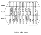
- An example of a layout with 19 channel structures is shown in Figure 1, but chips with up to 100, preferably 5 to 50 and in particular 10 to 25 channels are possible.
- the structuring of the, for example, 100 to 2000, preferably approximately 400 ⁇ m thick silicon wafer is preferably carried out by means of suitable microstructuring or etching techniques, for example reactive ion etching (“reactive ion etching”), as a result of which three-dimensional structures in silicon are independent of the crystal orientation can be manufactured [cf.
- reactive ion etching reactive ion etching
- the structures are characterized by dimensions of 50 to 1500, preferably 10 to 1000 ⁇ m and vertical walls, the depth of the channels being 20 to 1800 and preferably approximately 200 to 500 ⁇ m.
- the cross sections of a microreaction space which can differ from one another in the sense of the invention, are of the order of magnitude of 20 ⁇ 20 to 1500 ⁇ 1500 and in particular 100 ⁇ 100 to 300 ⁇ 300 ⁇ m 2 , as is also the case for example by Burns et al. in Trans IChemE 77 (5), 206 (1999) as being typical.
- the silicon wafer is etched through at the locations provided for this purpose.
- a closed SiO 2 layer on the surface of the reaction spaces or channels which preferably has a thickness of 50 to 2000, preferably 100 to 100 and in particular should have from about 200 to 400 nm.
- the thermal coating of a Si wafer with SiO 2 takes place by heating the wafer in an oxygen-containing atmosphere to approximately 1000 °. This leads to a reaction between silicon and oxygen with the formation of an oxide layer on the entire exposed surface, in particular also in the channel microstructures.
- the layer thickness of the SiO 2 can be adjusted depending on the duration of this thermal treatment.
- the oxidation is a root process, that is, the SiO 2 layer virtually grows into the wafer, and comes to a standstill at a certain depth, since there is no longer any silicon available for oxidation on the surface.
- the method is suitable for producing very dense and excellently adhering SiO 2 layers because they are materially connected to the silicon.
- the wafer remains bondable, ie it can still be connected to other wafers, for example made of glass or Si.
- other methods of coating are also suitable, for example PVD (physical vapor deposition) methods, as long as the material remains bondable.
- the structured silicon wafer which has been rendered inert by coating is finally connected to a further wafer, for example made of glass, preferably pyrex glass, by a suitable method, for example anodic bonding, and the individual flow channels are sealed off from one another.
- a further wafer for example made of glass, preferably pyrex glass, by a suitable method, for example anodic bonding, and the individual flow channels are sealed off from one another.
- the chip reactor is divided into one or more mixing zones, one or more reaction zones, one or more mixing and Reaction zones, one or more cooling zones or any combination thereof.
- the chip reactor preferably has three zones, namely two reaction zones and one cooling zone on, which in this case efficiently examines a two-stage reaction in the liquid phase can be.
- the mixing of two reactants takes place in the first zone as well as their reaction, in the second takes place the reaction between the product of the first Zone and another educt take place, while in the third the termination of the reaction is brought about by lowering the temperature. It is not mandatory that strictly separate the first and the second reaction zone thermally.
- zone 1 Reaction zone 2 takes place. Examples of this can be found in channels 16 and 19 according to Figure 1.
- the microreaction systems can be sequential or simultaneous, i.e. can be operated in parallel with defined educt quantities.
- microreaction systems can differ in their geometry in their geometry is the mixing angle at which the starting materials meet and which can be between 15 and 270 ° and preferably 45 to 180 °. Furthermore, it is possible to cool or heat each of the three zones independently of one another or to vary the temperature within a zone as desired, the reaction spaces in this example being channels whose length per zone can be 10 to 500 mm.
- the completion of the chip to the finished chip reactor takes place in a special embodiment in a sandwich construction, as shown in Figure 2.
- the chip is embedded in a manifold made of a suitable, preferably inert material, e.g. PTFE, which has the inlets for the educts, processes for the products on the underside for each microreaction system and, on the top, possibilities for visual inspection and thus for online reaction monitoring the glass wafer through to the different zones.
- the chip is covered on both sides with a flat seal, for example made of Gore-tex® GR10.
- the manifold for the educt feeds and product discharges also contains channels for guiding heat transfer fluids.
- the heat transfer takes place in such a way that the heat transfer medium on the back of the silicon wafer flows over the chip reactor and thus effectively transfers the heat of reaction that is generated or required in the reaction channels.
- a different heat transfer medium can be applied to each zone of the wafer.
- the temperature can also be regulated in any other way, for example by electrical heating.
- the temperatures in the individual zones can be set independently of one another.
- the heat transfer medium is connected to the manifold of the reactor, for example with hose connections.
- the chip reactor has a typical dimension of 50 x 50 to 150 x 150 mm.
- the fluid connections to the chip reactor can also be realized in another way.
- press fits are here by corresponding fluid inlets to the wafer (presented by Schwessinger, 4 th International Conference on Micro Reaction Technology, Atlanta / GA, 5-9 March 2000), or adhesive bonds, possibly with the help of small nozzles, called.
Abstract
Description
Die Erfindung befindet sich auf dem Gebiet der Mikroreaktionsbauteile und betrifft einen neuen Chipreaktor im Mikroformat zur raschen Ermittlung geeigneter geometrischer Parameter bzw. Ausführungsformen eines Mikroreaktors sowie geeigneter Reaktionsbedingungen für die Durchführung von Reaktionen im Mikromaßstab.The invention is in the field of microreaction components and relates to one new micro-sized chip reactor for quick determination of suitable geometric parameters or embodiments of a microreactor and suitable reaction conditions for performing reactions on a microscale.
Unter dem Begriff Mikrostrukturreaktor sind dem Fachmann Mikrostrukturapparate für chemische Prozesse geläufig, deren Kennzeichen es ist, dass mindestens eine der drei Raumdimensionen des Reaktionsraumes eine Abmessung im Bereich von 1 bis 2000 µm aufweist und die sich damit durch eine hohe übertragungsspezifische innere Oberfläche, kurze Verweilzeiten der Reaktanden und hohe spezifische Wärme- und Stofftransportleistungen auszeichnen. Beispielhaft sei auf die europäische Patentanmeldung EP 0903174 A1 (Bayer) verwiesen, in der die Flüssigphasenoxidation organischer Verbindungen in einem Mikroreaktor bestehend aus einer Schar von parallelen Reaktionskanälen beschrieben wird. Mikroreaktoren können dabei zusätzlich mikroelektronische Komponenten als integrale Bestandteile enthalten. Im Unterschied zu bekannten mikroanalytischen Systemen besteht bei den Mikroreaktoren keineswegs die Notwendigkeit, dass alle lateralen Dimensionen des Reaktionsraumes im µm-Bereich liegen. Vielmehr werden dessen Abmessungen ausschließlich durch die Art der Reaktion bestimmt. Dementsprechend kommen für bestimmte Reaktionen auch solche Mikroreaktoren in Frage, bei denen eine gewisse Zahl von Mikrokanälen gebündelt werden, so dass Mikro- und Makrokanäle bzw. paralleler Betrieb einer Vielzahl von Mikrokanälen nebeneinander vorliegen können. Vorzugsweise sind die Kanäle parallel zueinander angeordnet, um einen hohen Durchsatz zu ermöglichen und den Druckverlust so gering wie möglich zu halten.The term microstructure reactor is known to the person skilled in the art of microstructure apparatus for chemical processes, the characteristic of which is that at least one of the three spatial dimensions of the reaction space has a dimension in the range from 1 to 2000 μm and which is therefore characterized by a high transfer-specific inner surface and short dwell times Characterize reactants and high specific heat and mass transport performance. For example, reference is made to European patent application EP 0903174 A1 (Bayer), in which the liquid phase oxidation of organic compounds in a microreactor consisting of a family of parallel reaction channels is described. Microreactors can additionally contain microelectronic components as integral components. In contrast to known microanalytical systems, the microreactors in no way require that all lateral dimensions of the reaction space lie in the µm range. Rather, its dimensions are determined solely by the type of reaction. Accordingly, microreactors in which a certain number of microchannels are bundled are also suitable for certain reactions, so that microchannels and macrochannels or parallel operation of a multiplicity of microchannels can be present side by side. The channels are preferably arranged parallel to one another in order to enable a high throughput and to keep the pressure loss as low as possible.
Mikroreaktoren können ganz unterschiedliche Ausführungsformen aufweisen, d.h. sich in der geometrischen Anordnung der Reaktionsräume, deren geometrischer Abmessungen sowie der Art weitere Funktionselemente, z.B. statischer Mischer, unterscheiden. Dem Fachmann ist selbstverständlich klar, dass die Ausführungsform des Mikroreaktors einen unmittelbaren Einfluss auf Ausbeute und Selektivität der Reaktion besitzt. Um aber die geeignetste Ausführungsform für jede Reaktion zu ermitteln, besteht bislang nur die Möglichkeit, jeden einzelnen der bekannten, jeweils einzeln vorliegenden Mikroreaktoren zu testen, was freilich mit einem hohen Zeitaufwand verbunden ist.Microreactors can have very different embodiments, i.e. themselves in the geometric arrangement of the reaction spaces, their geometric dimensions and the type of other functional elements, e.g. static mixer. The specialist it is of course clear that the embodiment of the microreactor is an immediate one Has influence on the yield and selectivity of the reaction. But to the most suitable embodiment So far, it has only been possible to determine each reaction for each individual to test the known microreactors, which are present individually, which of course with takes a lot of time.
Die Aufgabe der vorliegenden Erfindung hat daher darin bestanden, diesem Umstand abzuhelfen und ein Bauteil zur Verfügung zu stellen, mit dessen Hilfe die optimale Ausführungsform eines Mikroreaktors sowie geeignete Reaktionsbedingungen in kürzester Zeit und mit geringstem technischen Aufwand ermittelt werden können.The object of the present invention was therefore to remedy this circumstance and to provide a component with the help of which the optimal embodiment a microreactor and suitable reaction conditions in the shortest possible time and with least technical effort can be determined.
Gegenstand der Erfindung ist ein Chip-Reaktor, bestehend aus einem Träger mit mindestens zwei in ihrer Ausführungsform unterschiedlichen Mikroreaktionssystemen ("Kanälen"), die jeweils mindestens einem Mikroreaktionsraum, mindestens einen Zulauf für die Edukte und mindestens einen Ablauf für die Produkte aufweisen, und dabei unabhängig voneinander betrieben oder genutzt werden können.The invention relates to a chip reactor consisting of a support with at least two microreaction systems ("channels") which are different in their embodiment, which in each case at least one microreaction space, at least one inlet for the starting materials and have at least one process for the products, and independently of each other can be operated or used.
Das Wesen der Erfindung besteht darin, dass sie exemplarisch in einem miniaturisierten Bauteil eine Vielzahl von denkbaren Ausführungsformen von Mikroreaktoren in sich vereinigt. Unter Ausführungsform soll in diesem Zusammenhang vor allem die geometrische Anordnung der Mikroreaktionssysteme bzw. -reaktionsräume (vorzugsweise Kanäle) sowie deren geometrische Abmessungen verstanden werden, aber auch die Art und Weise und der geometrische Ort, mit der die Vermischung der Reaktionspartner erfolgt. Als weitere Variable kommt die Möglichkeit hinzu, die Reaktion zonenweise unterschiedlich zu kühlen oder zu heizen. Auf diese Weise lassen sich eine Vielzahl von Prozessparametern variieren, wie beispielsweise die Eduktkonzentration, das Stoffmengenverhältnis der Edukte zueinander, der Einsatz von Lösungsmitteln und anderen Hilfsstoffen, die Durchsatzmengen, die Verweilzeit, unterschiedliche Verweilzeit in einzelnen Zonen sowie die Reaktionstemperaturen in den einzelnen Zonen. Der neue Chip-Reaktor bietet somit die Möglichkeit, durch problemloses Ansteuern der einzelnen Mikroreaktionsräume eine Vielzahl von möglichen Ausführungsformen von Mikroreaktionssystemen im Hinblick auf ihre Eignung in Flüssigphasenreaktionen und die Optimierung der Versuchsergebnisse zu erproben, um auf diesem Wege eine Vielzahl von Experimenten wesentlich schneller und mit geringerem Aufwand durchzuführen . The essence of the invention is that it is exemplified in a miniaturized Component combines a variety of conceivable embodiments of microreactors. In this context, the embodiment should primarily focus on the geometric arrangement the microreaction systems or reaction spaces (preferably channels) and their Geometric dimensions are understood, but also the way and the geometric Place where the reactants are mixed. As another variable there is also the possibility of cooling the reaction zone by zone differently heat. In this way, a variety of process parameters can be varied, such as the educt concentration, the molar ratio of the educts to one another, the Use of solvents and other auxiliaries, the throughput quantities, the residence time, different residence times in individual zones and the reaction temperatures in the individual Zones. The new chip reactor thus offers the possibility of easy control a large number of possible embodiments of the individual microreaction spaces of microreaction systems with regard to their suitability in liquid phase reactions and Optimization of the test results in order to test a variety of Perform experiments much faster and with less effort.
In einer beispielhaften Ausführungsform stellt der Chip-Reaktor einen Silizium-Glas-Verbund dar, in welchem die Struktur und Maße der Mikroreaktionssysteme vorgegeben sind. Alternative Materialkombinationen sind Silizium-Silizium, Glas-Glas, Metall-Metall, Metall-Kunststoff, Kunststoff-Kunststoff, oder Keramik-Keramik. Ein Beispiel für ein Layout mir 19 Kanalstrukturen ist in Abbildung 1 wiedergegeben, möglich sind jedoch Chips mit bis zu 100, vorzugsweise 5 bis 50 und insbesondere 10 bis 25 Kanälen. Die Strukturierung des beispielsweise 100 bis 2000, vorzugsweise etwa 400 µm starken Silizium-Wafers erfolgt dabei vorzugsweise mittels geeigneter Mikrostrukturierungs- bzw. Ätztechniken, z.B. dem reaktivem Ionen-Ätzen ("Reactive Ion Etching"), wodurch im Silizium dreidimensionale Strukturen unabhängig von der Kristallorientierung gefertigt werden können [vgl. James et al. in Sci. Am. 4, 248 (1993)]. Die Strukturen zeichnen sich dabei durch Abmessungen von 50 bis 1500, vorzugsweise 10 bis 1000 µm und senkrechte Wände aus, wobei die Tiefe der Kanäle 20 bis 1800 und vorzugsweise etwa 200 bis 500 µm beträgt. Die Querschnitte eines Mikroreaktionsraumes, die sich im Sinne der Erfindung voneinander unterscheiden können, liegen in der Größenordnung von 20×20 bis 1500×1500 und insbesondere 100×100 bis 300×300 µm2, wie dies beispielsweise auch von Burns et al. in Trans IChemE 77(5), 206 (1999) als typisch angegeben wird. Zur Versorgung der Mikroreaktionsräume mit Reaktanden wird der Silizium-Wafer an den dafür vorgesehenen Stellen durchgeätzt. Nach der Strukturierung des Silizium-Wafers hat es sich als in speziellen Ausführungsformen als vorteilhaft erwiesen, auf der Oberfläche der Reaktionsräume bzw. Kanäle eine geschlossene SiO2-Schicht zu erzeugen, welche vorzugsweise eine Stärke von 50 bis 2000, vorzugsweise 100 bis 100 und insbesondere von etwa 200 bis 400 nm aufweisen sollte. Auf diese Weise wird gewährleistet, dass es nicht zu Wechselwirkungen der Edukte oder Produkte mit der Si-Oberfläche und damit zu unerwünschten Neben- oder gar Zersetzungsreaktionen kommt, die ansonsten vielfach beobachtet werden. Die thermische Beschichtung eines Si-Wafers mit SiO2 erfolgt durch Erhitzen des Wafers in sauerstoffhaltiger Atmosphäre auf ca. 1000°. Damit kommt es zu einer Reaktion zwischen Silizium und Sauerstoff unter Ausbildung einer Oxidschicht auf der gesamten exponierten Oberfläche, also insbesondere auch in den Kanal-Mikrostrukturen. Je nach Dauer dieser thermischen Behandlung kann die Schichtdicke des SiO2 eingestellt werden. Bei der Oxidation handelt es sich um einen Wurzelprozess, d.h. die SiO2-Schicht wächst quasi in den Wafer hinein, und kommt bei einer bestimmten Tiefe zum Stillstand, da an der Oberfläche kein Silizium mehr zur Oxidation zur Verfügung steht. Das Verfahren ist geeignet, sehr dichte und exzellent haftende, weil stofflich mit dem Silizium verbundene SiO2-Schichten zu erzeugen. Außerdem bleibt der Wafer dabei bondbar, d.h. er kann weiterhin mit anderen Wafern, z.B. aus Glas oder Si verbunden werden. Generell sind auch andere Verfahren zur Beschichtung geeignet, z.B. PVD-Verfahren (Physical Vapor Deposition), solange das Material dabei bondbar bleibt. Zum Abschluss wird der strukturierte und durch Beschichtung inertisierte Silizium-Wafer schließlich durch ein geeignetes Verfahren, z.B. anodisches Bonden, mit einem weiteren Wafer, z.B. aus Glas, vorzugsweise Pyrex-Glas, verbunden und die einzelnen Strömungskanäle dicht zueinander verschlossen.In an exemplary embodiment, the chip reactor represents a silicon-glass composite, in which the structure and dimensions of the microreaction systems are predetermined. Alternative material combinations are silicon-silicon, glass-glass, metal-metal, metal-plastic, plastic-plastic, or ceramic-ceramic. An example of a layout with 19 channel structures is shown in Figure 1, but chips with up to 100, preferably 5 to 50 and in particular 10 to 25 channels are possible. The structuring of the, for example, 100 to 2000, preferably approximately 400 μm thick silicon wafer is preferably carried out by means of suitable microstructuring or etching techniques, for example reactive ion etching (“reactive ion etching”), as a result of which three-dimensional structures in silicon are independent of the crystal orientation can be manufactured [cf. James et al. in Sci. At the. 4 , 248 (1993)]. The structures are characterized by dimensions of 50 to 1500, preferably 10 to 1000 μm and vertical walls, the depth of the channels being 20 to 1800 and preferably approximately 200 to 500 μm. The cross sections of a microreaction space, which can differ from one another in the sense of the invention, are of the order of magnitude of 20 × 20 to 1500 × 1500 and in particular 100 × 100 to 300 × 300 μm 2 , as is also the case for example by Burns et al. in Trans IChemE 77 (5), 206 (1999) as being typical. To supply the microreaction spaces with reactants, the silicon wafer is etched through at the locations provided for this purpose. After the structuring of the silicon wafer, it has proven to be advantageous in special embodiments to produce a closed SiO 2 layer on the surface of the reaction spaces or channels, which preferably has a thickness of 50 to 2000, preferably 100 to 100 and in particular should have from about 200 to 400 nm. In this way it is ensured that there are no interactions of the starting materials or products with the Si surface and thus undesirable side reactions or even decomposition reactions, which are otherwise frequently observed. The thermal coating of a Si wafer with SiO 2 takes place by heating the wafer in an oxygen-containing atmosphere to approximately 1000 °. This leads to a reaction between silicon and oxygen with the formation of an oxide layer on the entire exposed surface, in particular also in the channel microstructures. The layer thickness of the SiO 2 can be adjusted depending on the duration of this thermal treatment. The oxidation is a root process, that is, the SiO 2 layer virtually grows into the wafer, and comes to a standstill at a certain depth, since there is no longer any silicon available for oxidation on the surface. The method is suitable for producing very dense and excellently adhering SiO 2 layers because they are materially connected to the silicon. In addition, the wafer remains bondable, ie it can still be connected to other wafers, for example made of glass or Si. In general, other methods of coating are also suitable, for example PVD (physical vapor deposition) methods, as long as the material remains bondable. Finally, the structured silicon wafer which has been rendered inert by coating is finally connected to a further wafer, for example made of glass, preferably pyrex glass, by a suitable method, for example anodic bonding, and the individual flow channels are sealed off from one another.
In einer bevorzugten Ausführungsform der Erfindung gliedert sich der Chip-Reaktor in eine
oder mehrere Mischzonen, eine oder mehrere Reaktionszonen, eine oder mehrere Mischund
Reaktionszonen, eine oder mehrere Kühlzonen oder beliebige Kombinationen davon.
Vorzugsweise weist der Chip-Reaktor drei Zonen, nämlich zwei Reaktions- und eine Kühlzone
auf, wodurch in diesem Fall eine zweistufige Reaktion in flüssiger Phase effizient untersucht
werden kann. In der ersten Zone erfolgt dabei die Vermischung zweier Reaktionsteilnehmer
sowie deren Reaktion, in der zweiten findet die Reaktion zwischen dem Produkt der ersten
Zone und einem weiteren Edukt statt, während in der dritten der Abbruch der Reaktion
durch Absenken der Temperatur bewirkt wird. Dabei ist es nicht zwingend erforderlich, die
erste und die zweite Reaktionszone thermisch streng voneinander zu trennen. Wenn nämlich
die Zugabe eines weiteren Reaktionspartners erforderlich ist oder anstelle eines Mischungspunktes
mehrere gewünscht werden, kann dies über die Zone 1 hinaus auch noch in der
Reaktionszone 2 stattfinden. Beispiele hierfür finden sich in den Kanälen 16 und 19 gemäß
Abbildung 1. Die Mikroreaktionssysteme können dabei sequentiell oder aber gleichzeitig, d.h.
parallel mit jeweils definierten Eduktmengen betrieben werden.In a preferred embodiment of the invention, the chip reactor is divided into one
or more mixing zones, one or more reaction zones, one or more mixing and
Reaction zones, one or more cooling zones or any combination thereof.
The chip reactor preferably has three zones, namely two reaction zones and one cooling zone
on, which in this case efficiently examines a two-stage reaction in the liquid phase
can be. The mixing of two reactants takes place in the first zone
as well as their reaction, in the second takes place the reaction between the product of the first
Zone and another educt take place, while in the third the termination of the reaction
is brought about by lowering the temperature. It is not mandatory that
strictly separate the first and the second reaction zone thermally. If namely
the addition of a further reactant is required or instead of a mixing point
if several are required, this can also be done in
Eine weitere Möglichkeit, wie sich die Mikroreaktionssysteme in ihrer Geometrie unterscheiden
können, besteht im Mischungswinkel, unter dem die Edukte aufeinander treffen und der
zwischen 15 und 270° und vorzugsweise 45 bis 180° liegen kann. Des weiteren ist es möglich,
jede der drei Zonen unabhängig voneinander zu kühlen oder zu heizen bzw. die Temperatur
innerhalb einer Zone beliebig zu variieren, wobei die Reaktionsräume in diesem Beispiel
Kanäle darstellen, deren Länge pro Zone 10 bis 500 mm betragen kann. In Tabelle 1
sind die Geometrien der Kanalsysteme gemäß Abbildung 1 näher erläutert:
Die Komplettierung des Chips zum fertigen Chip-Reaktor erfolgt in einer besonderen Ausfürhungsform in Sandwich-Bauweise, wie sie in Abbildung 2 wiedergegeben ist. Der Chip ist dabei eingebettet in einem Manifold aus einem geeigneten vorzugsweise inerten Material, z.B. PTFE, welches an der Unterseite für jedes Mikroreaktionssystem die Zuläufe für die Edukte, Abläufe für die Produkte und an der Oberseite Möglichkeiten zur optischen Einsicht und damit zum online-Reaktionsmonitoring durch den Glas-Wafer hindurch auf die unterschiedlichen Zonen besitzt. Der Chip wird dabei von beiden Seiten mit einer Flachdichtung, beispielsweise aus dem Material Gore-tex® GR10 belegt. Das Manifold für die Edukt-Zuführungen und Produkt-Abführungen enthält dabei zusätzlich noch Kanäle für die Führung von Wärmeträger-Flüssigkeiten. Der Wärmeübergang erfolgt dabei so, dass der Wärmeträger auf der Rückseite des Silizium-Wafers über den Chip-Reaktor fließt und damit die in den Reaktionskanälen entstehende oder erforderliche Reaktionswärme effektiv überträgt. Jede Zone des Wafers kann dabei mit einem anderen Wärmeträger beaufschlagt werden. Die Regulierung der Temperatur kann dabei grundsätzlich auch auf jedem anderen Wege, beispielsweise durch elektrische Beheizung erzielt werden. Die Temperaturen in den einzelnen Zonen können unabhängig voneinander eingestellt werden. Der Anschluss der Wärmeträger an das Manifold des Reaktors erfolgt dabei z.B. mit Schlauchanschlüssen. Der Chip-Reaktor besitzt eine typische Abmessung von 50 x 50 bis 150 x 150 mm. Die Realisierung der Fluidanschlüsse an den Chip-Reaktor kann auch auf andere Art und Weise erfolgen. Beispielsweise seien hier Presssitze von entsprechenden Fluidzuführungen an den Wafer (vorgestellt von Schwesinger, 4th International Conference on Microreaction Technology, Atlanta/GA, 5-9 März 2000) oder auch Klebverbindungen, unter Umständen mit Hilfe kleiner Stutzen, genannt.The completion of the chip to the finished chip reactor takes place in a special embodiment in a sandwich construction, as shown in Figure 2. The chip is embedded in a manifold made of a suitable, preferably inert material, e.g. PTFE, which has the inlets for the educts, processes for the products on the underside for each microreaction system and, on the top, possibilities for visual inspection and thus for online reaction monitoring the glass wafer through to the different zones. The chip is covered on both sides with a flat seal, for example made of Gore-tex® GR10. The manifold for the educt feeds and product discharges also contains channels for guiding heat transfer fluids. The heat transfer takes place in such a way that the heat transfer medium on the back of the silicon wafer flows over the chip reactor and thus effectively transfers the heat of reaction that is generated or required in the reaction channels. A different heat transfer medium can be applied to each zone of the wafer. In principle, the temperature can also be regulated in any other way, for example by electrical heating. The temperatures in the individual zones can be set independently of one another. The heat transfer medium is connected to the manifold of the reactor, for example with hose connections. The chip reactor has a typical dimension of 50 x 50 to 150 x 150 mm. The fluid connections to the chip reactor can also be realized in another way. For example, press fits are here by corresponding fluid inlets to the wafer (presented by Schwessinger, 4 th International Conference on Micro Reaction Technology, Atlanta / GA, 5-9 March 2000), or adhesive bonds, possibly with the help of small nozzles, called.
Claims (18)
Applications Claiming Priority (2)
| Application Number | Priority Date | Filing Date | Title |
|---|---|---|---|
| DE10106952 | 2001-02-15 | ||
| DE10106952A DE10106952C2 (en) | 2001-02-15 | 2001-02-15 | Chip reactor |
Publications (2)
| Publication Number | Publication Date |
|---|---|
| EP1232785A2 true EP1232785A2 (en) | 2002-08-21 |
| EP1232785A3 EP1232785A3 (en) | 2004-01-21 |
Family
ID=7674081
Family Applications (1)
| Application Number | Title | Priority Date | Filing Date |
|---|---|---|---|
| EP02002659A Ceased EP1232785A3 (en) | 2001-02-15 | 2002-02-06 | Chip-reactor |
Country Status (3)
| Country | Link |
|---|---|
| US (1) | US20030003024A1 (en) |
| EP (1) | EP1232785A3 (en) |
| DE (1) | DE10106952C2 (en) |
Cited By (1)
| Publication number | Priority date | Publication date | Assignee | Title |
|---|---|---|---|---|
| WO2007012632A1 (en) * | 2005-07-25 | 2007-02-01 | Siemens Aktiengesellschaft | Microfluid system |
Families Citing this family (6)
| Publication number | Priority date | Publication date | Assignee | Title |
|---|---|---|---|---|
| DE10206708B4 (en) * | 2002-02-18 | 2005-12-22 | P21 - Power For The 21St Century Gmbh | Microchannel system |
| KR20080010395A (en) * | 2005-04-26 | 2008-01-30 | 아비자 테크놀로지 리미티드 | Microfluidic structures and how to make them |
| HU227586B1 (en) | 2005-12-23 | 2011-08-29 | Thales Rt | Method for forming sealed channel of microfluidical reactor and microfluidical reactor containing the same |
| EP1854425A1 (en) * | 2006-05-11 | 2007-11-14 | BrainLAB AG | Position determination for medical devices with redundant position measurement and weighting to prioritise measurements |
| CN102553480B (en) * | 2011-12-26 | 2014-01-22 | 溧阳市澳谷信息科技有限公司 | Micro mixer |
| CN108164389B (en) * | 2018-01-29 | 2020-07-10 | 浙江大学 | Synthesis method and synthesis reactor of high-selectivity 2-methylallyl chloride |
Citations (4)
| Publication number | Priority date | Publication date | Assignee | Title |
|---|---|---|---|---|
| US5580523A (en) * | 1994-04-01 | 1996-12-03 | Bard; Allen J. | Integrated chemical synthesizers |
| WO1999034909A1 (en) * | 1998-01-06 | 1999-07-15 | Central Research Laboratories Limited | Method of forming interconnections between channels and chambers |
| WO1999041015A1 (en) * | 1998-02-11 | 1999-08-19 | Institut für Physikalische Hochtechnologie e.V. | Miniaturized temperature-zone flow reactor |
| EP1125630A2 (en) * | 2000-02-14 | 2001-08-22 | CPC Cellular Process Chemistry Systems GmbH | Microreactor with improved heat exchanger |
Family Cites Families (7)
| Publication number | Priority date | Publication date | Assignee | Title |
|---|---|---|---|---|
| US5595712A (en) * | 1994-07-25 | 1997-01-21 | E. I. Du Pont De Nemours And Company | Chemical mixing and reaction apparatus |
| US5585069A (en) * | 1994-11-10 | 1996-12-17 | David Sarnoff Research Center, Inc. | Partitioned microelectronic and fluidic device array for clinical diagnostics and chemical synthesis |
| DE19648695C2 (en) * | 1996-11-25 | 1999-07-22 | Abb Patent Gmbh | Device for the automatic and continuous analysis of liquid samples |
| US6143152A (en) * | 1997-11-07 | 2000-11-07 | The Regents Of The University Of California | Microfabricated capillary array electrophoresis device and method |
| EP1113869B1 (en) * | 1999-03-03 | 2005-01-26 | Symyx Technologies, Inc. | Chemical processing microsystems for evaluating heterogeneously catalyzed reactions and using same |
| US6701774B2 (en) * | 2000-08-02 | 2004-03-09 | Symyx Technologies, Inc. | Parallel gas chromatograph with microdetector array |
| DE10106953B4 (en) * | 2001-02-15 | 2006-07-06 | Cognis Ip Management Gmbh | microreactors |
-
2001
- 2001-02-15 DE DE10106952A patent/DE10106952C2/en not_active Expired - Fee Related
-
2002
- 2002-02-06 EP EP02002659A patent/EP1232785A3/en not_active Ceased
- 2002-02-14 US US10/075,726 patent/US20030003024A1/en not_active Abandoned
Patent Citations (4)
| Publication number | Priority date | Publication date | Assignee | Title |
|---|---|---|---|---|
| US5580523A (en) * | 1994-04-01 | 1996-12-03 | Bard; Allen J. | Integrated chemical synthesizers |
| WO1999034909A1 (en) * | 1998-01-06 | 1999-07-15 | Central Research Laboratories Limited | Method of forming interconnections between channels and chambers |
| WO1999041015A1 (en) * | 1998-02-11 | 1999-08-19 | Institut für Physikalische Hochtechnologie e.V. | Miniaturized temperature-zone flow reactor |
| EP1125630A2 (en) * | 2000-02-14 | 2001-08-22 | CPC Cellular Process Chemistry Systems GmbH | Microreactor with improved heat exchanger |
Cited By (4)
| Publication number | Priority date | Publication date | Assignee | Title |
|---|---|---|---|---|
| WO2007012632A1 (en) * | 2005-07-25 | 2007-02-01 | Siemens Aktiengesellschaft | Microfluid system |
| KR100942069B1 (en) * | 2005-07-25 | 2010-02-12 | 지멘스 악티엔게젤샤프트 | Microfluid system |
| CN101227972B (en) * | 2005-07-25 | 2010-11-10 | 西门子公司 | Microfluid system |
| US8146650B2 (en) | 2005-07-25 | 2012-04-03 | Siemens Aktiengesellschaft | Microfluidic system |
Also Published As
| Publication number | Publication date |
|---|---|
| EP1232785A3 (en) | 2004-01-21 |
| DE10106952A1 (en) | 2002-09-05 |
| US20030003024A1 (en) | 2003-01-02 |
| DE10106952C2 (en) | 2003-01-16 |
Similar Documents
| Publication | Publication Date | Title |
|---|---|---|
| EP1054735B1 (en) | Miniaturized temperature-zone flow reactor | |
| DE69533554T2 (en) | LIQUID DISTRIBUTION SYSTEM | |
| DE69732855T2 (en) | SYSTEM FOR DISTRIBUTING LIQUIDS | |
| DE60223193T2 (en) | Production of integrated fluidic devices | |
| DE19917148C2 (en) | Process and micromixer for producing a dispersion | |
| DE60108482T2 (en) | PROCESS OPTIMIZING REACTOR WITH PARALLEL FLOW | |
| DE10106953B4 (en) | microreactors | |
| DE60200822T2 (en) | Microdosing and sampling device and microchip with this device | |
| DE60311941T2 (en) | CONTAINER FOR THE POLYMERASE CHAIN REACTION AND METHOD FOR THE PRODUCTION THEREOF | |
| DE10123092B4 (en) | Method and static mixer for mixing at least two fluids | |
| DE19748481C2 (en) | Static micromixer | |
| DE4416343A1 (en) | Static micro mixer | |
| DE10309583A1 (en) | Microplate with an integrated microfluidic system for parallel processing of tiny fluid volumes | |
| EP1031375B1 (en) | Microreactor | |
| DE19541265A1 (en) | Process for the preparation of dispersions and for carrying out chemical reactions with a disperse phase | |
| DE60201257T2 (en) | METHOD AND DEVICE FOR CONTINUOUSLY IMPLEMENTING A BIOLOGICAL, CHEMICAL OR BIOCHEMICAL REACTION | |
| DE10106952C2 (en) | Chip reactor | |
| EP2090353B1 (en) | Reaction mixing system for mixing and chemical reaction of at least two fluids | |
| DE112015000711B4 (en) | Manufacturing of microfluidic probe heads | |
| EP1125630B1 (en) | Microreactor with improved heat exchanger | |
| WO2001089693A1 (en) | Emulsifying and separating device for liquid phases | |
| DE10103425A1 (en) | Mixing method, to mix or homogenize microscopic or macroscopic flows, has parallel flow planes with serpentine flow paths and separation plane with passage openings, to connect flows by alternating eddy part-flows | |
| DE10005549A1 (en) | Microreactor for reaction media in the form of a suspension | |
| EP1329258A2 (en) | Microreactor for reactions with volatile or gaseous products | |
| EP2318108A1 (en) | Device and process for substance separation in a microstructured apparatus |
Legal Events
| Date | Code | Title | Description |
|---|---|---|---|
| PUAI | Public reference made under article 153(3) epc to a published international application that has entered the european phase |
Free format text: ORIGINAL CODE: 0009012 |
|
| 17P | Request for examination filed |
Effective date: 20020206 |
|
| AK | Designated contracting states |
Kind code of ref document: A2 Designated state(s): AT BE CH CY DE DK ES FI FR GB GR IE IT LI LU MC NL PT SE TR |
|
| AX | Request for extension of the european patent |
Free format text: AL;LT;LV;MK;RO;SI |
|
| RIN1 | Information on inventor provided before grant (corrected) |
Inventor name: HOENICKE, DIETER, PROF. DR. Inventor name: ZECH, TORSTEN |
|
| PUAL | Search report despatched |
Free format text: ORIGINAL CODE: 0009013 |
|
| AK | Designated contracting states |
Kind code of ref document: A3 Designated state(s): AT BE CH CY DE DK ES FI FR GB GR IE IT LI LU MC NL PT SE TR |
|
| AX | Request for extension of the european patent |
Extension state: AL LT LV MK RO SI |
|
| RIC1 | Information provided on ipc code assigned before grant |
Ipc: 7B 01L 7/00 B Ipc: 7B 01F 13/00 B Ipc: 7B 01F 5/06 B Ipc: 7B 01J 19/00 A |
|
| AKX | Designation fees paid |
Designated state(s): AT BE CH CY DE DK ES FI FR GB GR IE IT LI LU MC NL PT SE TR |
|
| RAP1 | Party data changed (applicant data changed or rights of an application transferred) |
Owner name: COGNIS IP MANAGEMENT GMBH |
|
| STAA | Information on the status of an ep patent application or granted ep patent |
Free format text: STATUS: THE APPLICATION HAS BEEN REFUSED |
|
| 18R | Application refused |
Effective date: 20120607 |