EP1385205A2 - Moisture-sensitive device protection system - Google Patents
Moisture-sensitive device protection system Download PDFInfo
- Publication number
- EP1385205A2 EP1385205A2 EP03077071A EP03077071A EP1385205A2 EP 1385205 A2 EP1385205 A2 EP 1385205A2 EP 03077071 A EP03077071 A EP 03077071A EP 03077071 A EP03077071 A EP 03077071A EP 1385205 A2 EP1385205 A2 EP 1385205A2
- Authority
- EP
- European Patent Office
- Prior art keywords
- integrated circuit
- moisture
- desiccant
- inner cavity
- inner walls
- Prior art date
- Legal status (The legal status is an assumption and is not a legal conclusion. Google has not performed a legal analysis and makes no representation as to the accuracy of the status listed.)
- Withdrawn
Links
Images


Classifications
-
- H—ELECTRICITY
- H01—ELECTRIC ELEMENTS
- H01L—SEMICONDUCTOR DEVICES NOT COVERED BY CLASS H10
- H01L23/00—Details of semiconductor or other solid state devices
- H01L23/16—Fillings or auxiliary members in containers or encapsulations, e.g. centering rings
- H01L23/18—Fillings characterised by the material, its physical or chemical properties, or its arrangement within the complete device
- H01L23/26—Fillings characterised by the material, its physical or chemical properties, or its arrangement within the complete device including materials for absorbing or reacting with moisture or other undesired substances, e.g. getters
-
- H—ELECTRICITY
- H01—ELECTRIC ELEMENTS
- H01L—SEMICONDUCTOR DEVICES NOT COVERED BY CLASS H10
- H01L2924/00—Indexing scheme for arrangements or methods for connecting or disconnecting semiconductor or solid-state bodies as covered by H01L24/00
- H01L2924/0001—Technical content checked by a classifier
- H01L2924/0002—Not covered by any one of groups H01L24/00, H01L24/00 and H01L2224/00
Definitions
- the present invention relates generally to integrated circuits, and more particularly, to apparatuses and methods of extending the life of moisture-sensitive devices.
- Integrated circuits are commonly used in various electronic systems, including computer-based systems, logic based systems, control systems, and other systems known in the art. During production and manufacturing of these systems, ICs may remain unused (e.s. in inventory) for extended periods of time, where they can be exposed to environmental conditions, such as, humidity and moisture. The moisture typically can be in the form of water vapor in air. Exposure to moisture typically can occur during production downtime, for example, during production "change-overs" or during small quantity production of an electronic system, where continuous production is not required. Of course, exposure to the elements, such as moisture, may also occur during other production downtime events, which are experienced in conventional manufacturing and assembly operations.
- Each IC includes a silicon device within a mold, typically formed of a plastic material.
- Each IC has a corresponding moisture sensitivity level with an associated maximum exposure time.
- the sensitivity levels and exposure times, as well as, staying the maximum exposure time have associated industry standard requirements.
- the IC is typically discarded or baked for an extended period of time. Discarding of ICs, causes wasted expense and baking of ICs can have associated disadvantages, as stated in detail below.
- a typical series of manufacturing steps, for an electronic system, stated above, are as follows. First, a tape reel or tray of ICs is removed from an airtight moisture barrier bag, for use in an assembly machine. Once the bag is opened to begin manufacturing, the components have a limited useful life. Next, The ICs are placed onto a printed circuit board having a solder paste pattern to form an electronic system assembly. Finally, the electronic system assembly is placed into a reflow oven, to melt the solder and form solder bonds between the ICs and the printed circuit board.
- a first method includes placing the IC in a "Dry Box", which prevents further exposure to moisture, during downtime.
- a disadvantage with the dry box is that the moisture that previously entered the IC, remains in the IC, which may cause operating intermittence. Also, potential future industry standards, prohibiting the use of dry-boxes, may be introduced due to the potential associated intermittence.
- Another method includes baking the IC for a period of time to remove moisture that has entered the mold. By baking the IC, the moisture penetration process is reversed. Obviously, this baking is time consuming, not cost effective, and can cause oxydation of solder coating on IC leads, degrading the ability to have a solder joint formed to the IC.
- the ICs can be reinserted into moisture barrier bags, during downtime, although is also time consuming and requires a supply of moisture barrier bags and desiccant material, as well as a sealing apparatus.
- the present invention provides apparatuses and methods of extending the life of moisture-sensitive devices.
- Integrated circuit moisture resistant apparatuses are provided for preventing moisture absorption by an integrated circuit.
- the moisture resistant apparatuses include at least one integrated circuit housing that has a plurality of inner walls, which form at least one inner cavity.
- a desiccant body is coupled to at least a portion of the plurality of inner walls and absorbs moisture within the inner cavities.
- a method for performing the same is provided.
- a manufacturing method of preventing moisture absorption by an integrated circuit is provided.
- One of several advantages of the present invention is that it provides a desiccant body within the integrated circuit housing, which absorbs moisture within the inner cavity.
- the presence of the desiccant body within the integrated circuit housing prevents absorption of moisture by an integrated circuit mold. This increases the floor life of the integrated circuits.
- Another advantage of the present invention is that it is versatile in application. It may be applied to multiple style integrated circuits and integrated circuit housings and may be applied using multiple methods.
- the present invention provides multiple methods of preventing moisture absorption of an integrated circuit mold that consumes a minimal amount of time and is cost effective.
- the same reference numerals are used to refer to the same components. While the present invention is described with respect to methods and apparatuses for preventing moisture absorption by an integrated circuit, the present invention may be applied in various manufacturing and production processes. It is also understood that the present invention may be applied in assembly of various systems including: electronic systems, control systems, computer-based systems, logic-based systems, and other systems known in the art.
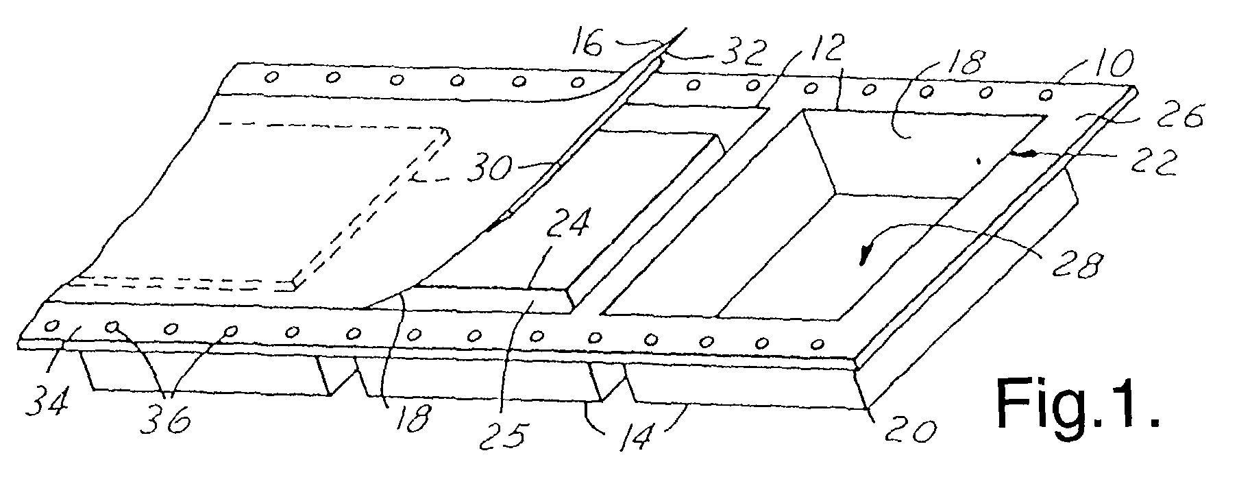
- the moisture resistant apparatuses 10 include at least one housing 12, where each housing 12 has a lower portion 14 and an upper portion 16.
- the lower portion 14 has multiple inner walls 18 that form an integrated circuit pocket 20.
- the pocket 20 has an open side 22 for an integrated circuit 24 to be inserted and removed therethrough.
- the integrated circuit 24 has an integrated circuit mold 25.
- the upper portion 16 is coupled to an upper side 26 of and forms an inner cavity 28 with the lower portion 14.
- a desiccant body 30 is coupled to the housing 12 and resides within the inner cavity 28.
- the desiccant body 30 is coupled to an inner side 32 of the upper portion 16. In another embodiment of the present invention, as illustrated by Figures 3 and 4, the desiccant body 30 is coupled to the lower portion 14.
- the moisture resistant apparatuses 10 of Figures 1 and 3 are shown in the form of a tape, having flanges 34 and flange holes 36, which may be wound onto a reel, the moisture resistant apparatuses 10 may be of various forms.
- the moisture resistant apparatuses 10 may be in the form of integrated circuit reels, integrated circuit trays, or other forms known in the art.
- the housing 12 may also be in various forms, styles, shapes, and sizes known in the art.
- the housing 12, including the inner walls 18, may be formed of a plastic moisture permeable material, as traditionally used or may be formed of a moisture impermeable or moisture resistant material.
- the moisture resistant material aids in preventing moisture from entering the inner cavity 28 and potentially being absorbed by an integrated circuit mold.
- the inner walls 18 may form or be integrally part of an integrated circuit tape, as shown.
- the lower portion 14 and the upper portion 16 may also be in a form of an integrated circuit tape, as shown.
- the upper portion 16 covers the open side 22 and is coupled to the lower portion 14 by a sealant layer 38, which forms a seal 40.
- the sealant layer 38 may be in the form of an adhesive or other sealant material known in the art.
- the seal 40 may include a weld, known in the art as a heat seal, of upper portion 16 to lower portion 14, in which case no additional sealant material is required.
- the seal 40 prevents moisture from entering the inner cavity 28 through the seal 40.
- the pocket 20 has a depth D that accommodates a desiccant body thickness T and an integrated circuit height H.
- the depth D varies depending upon integrated circuit type and style and desiccant body thickness T.
- the desiccant body 30 may be of various forms including: a desiccant layer, a desiccant coating, a desiccant wafer, desiccant film, a desiccant paper, a desiccant tape, a desiccant material, a desiccant deposit, or other desiccant body known in the art.
- desiccant paper and desiccant tape are Drikette® Desiccant Paper and Desimax TM Sorbent Loaded Film Desiccant Tape, respectively, by Multisorb Technologies Inc.
- the desiccant body 30 is formed of cellulose fiber and silica gel.
- the desiccant body 30 may be of various styles, shapes, sizes, and forms.
- the desiccant body 30 also minimizes the potential for delamination of integrated circuit wire bonds within the mold 25.
- FIG. 5 a logic flow diagram illustrating a method of preventing moisture absorption by the integrated circuit 24 in accordance with an embodiment of the present invention is shown.
- the housing 12 is formed, including the inner walls 18 to form the inner cavity 28.
- the housing 12 may be formed using methods known in the art.
- the housing 12 may be in the form of a tape, a tray, a cartridge, or other integrated circuit housing form.
- the housing 12 may be formed of moisture impermeable material, unlike integrated circuit housings of prior art. The moisture impermeable material, as stated above, prevents moisture from entering the inner cavity 28 and potentially being absorbed by the integrated circuit mold 25.
- a desiccant body 30 is coupled to a portion of the inner walls 18 or a portion of the integrated circuit 24.
- the desiccant body 30 may be inserted into the inner cavity 28, as shown by Figures 3 and 4, or applied to an inner wall 18, as shown by Figures 1 and 2.
- the desiccant body 30 may also be applied or attached to the integrated circuit 24 before being inserted into the inner cavity 28.
- the desiccant body 30 may be molded onto, applied to, adhesively attached to, or coupled to a portion of the inner walls 18, the integrated circuit 24, or a combination thereof.
- the housing 12 or the integrated circuit 24 and the desiccant body 30 may be baked, using baking methods known in the art, upon application of the desiccant body 30 to the inner walls 18, to activate the desiccant body 30 by removing absorbed moisture from the desiccant body 30.
- step 106 the integrated circuit 24 as well as the desiccant body 30, when attached to the integrated circuit 24, is inserted into the inner cavity 28.
- the housing 12 is sealed.
- the lower portion 14 is sealed to the upper portion 16.
- the lower portion 14 may be sealed to the upper portion 16 via the sealant layer 38, an adhesive, by negatively pressurizing the inner cavity 28, by a mechanical coupling, or by other sealing methods known in the art.
- sealing the upper portion 16 to the lower portion 14 further prevents moisture from entering the inner cavity 28, and potentially the integrated circuit 24.
- FIG. 6 a logic flow diagram illustrating a manufacturing method of preventing moisture absorption by the integrated circuit 24 in accordance with an embodiment of the present invention is shown.
- step 150 the integrated circuit moisture resistant apparatuses 10 are removed from a container.
- the container may be an airtight moisture resistant bag or other container or storage device known in the art.
- step 152 assembly of an electronic system is initiated.
- the integrated circuit moisture resistant apparatuses 10 enter an electronic system assembly machine, where upon the integrated circuit 24 may remain in the housing 12 or may be attached to a printed circuit board, not shown.
- step 154 when the integrated circuit 24 remains in the housing 12, moisture is absorbed in the inner cavity 28 by the desiccant body 30, thereby preventing moisture absorption by the integrated circuit mold 25.
- step 156 the integrated circuit 24 is maintained in the integrated circuit moisture resistant apparatuses 10 until assembly usage thereof.
- the integrated circuit 24 remains in the housing 12 to prevent moisture absorption by the integrated circuit mold 25.
- the present invention provides multiple methods and apparatuses for preventing moisture absorption by an integrated circuit mold.
- the present invention by minimizing the moisture absorption of an integrated circuit, minimizes future operating intermittence and increases the life of the integrated circuit.
- the present invention also does not require the use of a dry-box during assembly, or downtime, of an electronic system due to the moisture absorption characteristics of the integrated circuit moisture resistant apparatuses.
- the present invention minimizes the need to bake the integrated circuit, thereby minimizing problems associated therein.
Abstract
Description
- The present invention relates generally to integrated circuits, and more particularly, to apparatuses and methods of extending the life of moisture-sensitive devices.
- Integrated circuits (ICs) are commonly used in various electronic systems, including computer-based systems, logic based systems, control systems, and other systems known in the art. During production and manufacturing of these systems, ICs may remain unused (e.s. in inventory) for extended periods of time, where they can be exposed to environmental conditions, such as, humidity and moisture. The moisture typically can be in the form of water vapor in air. Exposure to moisture typically can occur during production downtime, for example, during production "change-overs" or during small quantity production of an electronic system, where continuous production is not required. Of course, exposure to the elements, such as moisture, may also occur during other production downtime events, which are experienced in conventional manufacturing and assembly operations.
- Each IC includes a silicon device within a mold, typically formed of a plastic material. Each IC has a corresponding moisture sensitivity level with an associated maximum exposure time. The sensitivity levels and exposure times, as well as, staying the maximum exposure time, have associated industry standard requirements. When an IC has exceeded an industry standard requirement, the IC is typically discarded or baked for an extended period of time. Discarding of ICs, causes wasted expense and baking of ICs can have associated disadvantages, as stated in detail below.
- A typical series of manufacturing steps, for an electronic system, stated above, are as follows. First, a tape reel or tray of ICs is removed from an airtight moisture barrier bag, for use in an assembly machine. Once the bag is opened to begin manufacturing, the components have a limited useful life. Next, The ICs are placed onto a printed circuit board having a solder paste pattern to form an electronic system assembly. Finally, the electronic system assembly is placed into a reflow oven, to melt the solder and form solder bonds between the ICs and the printed circuit board.
- ICs that have been exposed for extended periods of time to levels of moisture typically found in air at most production and manufacturing facilities, are vulnerable to internal damage when processed in a reflow oven. This vulnerability requires special handling methods that increase manufacturing costs.
- When an IC is exposed to moisture, a moisture permeating process begins. Moisture penetrates into the mold and gradually reaches a center cavity, where the IC resides therein. When the IC is baked, due to the moisture level of the molding compound, delamination of mold from the silicon device can occur, with consequent breaking of wire bonds. The broken wire bonds cause intermittence during post assembly operating use of the IC. Although ICs are tested upon completion of assembly before being used as intended, the delamination may be undetectable, since the silicon device wire bonds may be resting on or touching silicon device contacts even though a wire bond no longer exists.
- An IC maximum exposure time can be stayed using several methods. A first method includes placing the IC in a "Dry Box", which prevents further exposure to moisture, during downtime. A disadvantage with the dry box is that the moisture that previously entered the IC, remains in the IC, which may cause operating intermittence. Also, potential future industry standards, prohibiting the use of dry-boxes, may be introduced due to the potential associated intermittence. Another method includes baking the IC for a period of time to remove moisture that has entered the mold. By baking the IC, the moisture penetration process is reversed. Obviously, this baking is time consuming, not cost effective, and can cause oxydation of solder coating on IC leads, degrading the ability to have a solder joint formed to the IC. As another method, the ICs can be reinserted into moisture barrier bags, during downtime, although is also time consuming and requires a supply of moisture barrier bags and desiccant material, as well as a sealing apparatus.
- It would therefore be desirable to develop a method of reducing the amount of moisture exposure of ICs during manufacturing and production processes, which does not require special handling and is cost effective.
- The present invention provides apparatuses and methods of extending the life of moisture-sensitive devices. Integrated circuit moisture resistant apparatuses are provided for preventing moisture absorption by an integrated circuit. The moisture resistant apparatuses include at least one integrated circuit housing that has a plurality of inner walls, which form at least one inner cavity. A desiccant body is coupled to at least a portion of the plurality of inner walls and absorbs moisture within the inner cavities. A method for performing the same is provided. Also, a manufacturing method of preventing moisture absorption by an integrated circuit is provided.
- One of several advantages of the present invention is that it provides a desiccant body within the integrated circuit housing, which absorbs moisture within the inner cavity. The presence of the desiccant body within the integrated circuit housing prevents absorption of moisture by an integrated circuit mold. This increases the floor life of the integrated circuits.
- Another advantage of the present invention is that it is versatile in application. It may be applied to multiple style integrated circuits and integrated circuit housings and may be applied using multiple methods.
- Furthermore, the present invention provides multiple methods of preventing moisture absorption of an integrated circuit mold that consumes a minimal amount of time and is cost effective.
- Other advantages and features of the present invention will become apparent when viewed in light of the detailed description of the preferred embodiment when taken in conjunction with the attached drawings and appended claims.
-
- Figure 1 is a perspective view of a first integrated circuit moisture resistant apparatus in accordance with an embodiment of the present invention;
- Figure 2 is a cross-sectional view of the first integrated circuit moisture resistant apparatus in accordance with an embodiment of the present invention;
- Figure 3 is a perspective view of a second integrated circuit moisture resistant apparatus in accordance with an embodiment of the present invention;
- Figure 4 is a cross-sectional view of the second integrated circuit moisture resistant apparatus in accordance with an embodiment of the present invention;
- Figure 5 is a logic flow diagram illustrating a method of preventing moisture absorption by an integrated circuit in accordance with an embodiment of the present invention; and
- Figure 6 is a logic flow diagram illustrating a manufacturing method of preventing moisture absorption by an integrated circuit in accordance with an embodiment of the present invention.
-
- In each of the following figures, the same reference numerals are used to refer to the same components. While the present invention is described with respect to methods and apparatuses for preventing moisture absorption by an integrated circuit, the present invention may be applied in various manufacturing and production processes. It is also understood that the present invention may be applied in assembly of various systems including: electronic systems, control systems, computer-based systems, logic-based systems, and other systems known in the art.
- In the following description, various operating parameters and components are described for one constructed embodiment. These specific parameters and components are included as examples and are not meant to be limiting.
- Referring now to Figures 1-4, perspective views and cross-sectional views of integrated circuit moisture
resistant apparatuses 10, are shown, in accordance with an embodiment of the present invention. The moistureresistant apparatuses 10 include at least onehousing 12, where eachhousing 12 has alower portion 14 and anupper portion 16. Thelower portion 14 has multipleinner walls 18 that form anintegrated circuit pocket 20. Thepocket 20 has anopen side 22 for anintegrated circuit 24 to be inserted and removed therethrough. Theintegrated circuit 24 has an integratedcircuit mold 25. Theupper portion 16 is coupled to anupper side 26 of and forms aninner cavity 28 with thelower portion 14. Adesiccant body 30 is coupled to thehousing 12 and resides within theinner cavity 28. In one embodiment of the present invention, as illustrated in Figures 1 and 2, thedesiccant body 30 is coupled to an inner side 32 of theupper portion 16. In another embodiment of the present invention, as illustrated by Figures 3 and 4, thedesiccant body 30 is coupled to thelower portion 14. - Although, the moisture
resistant apparatuses 10 of Figures 1 and 3 are shown in the form of a tape, havingflanges 34 and flange holes 36, which may be wound onto a reel, the moistureresistant apparatuses 10 may be of various forms. For example, the moistureresistant apparatuses 10 may be in the form of integrated circuit reels, integrated circuit trays, or other forms known in the art. - The
housing 12 may also be in various forms, styles, shapes, and sizes known in the art. Thehousing 12, including theinner walls 18, may be formed of a plastic moisture permeable material, as traditionally used or may be formed of a moisture impermeable or moisture resistant material. The moisture resistant material aids in preventing moisture from entering theinner cavity 28 and potentially being absorbed by an integrated circuit mold. Theinner walls 18 may form or be integrally part of an integrated circuit tape, as shown. - The
lower portion 14 and theupper portion 16 may also be in a form of an integrated circuit tape, as shown. Theupper portion 16 covers theopen side 22 and is coupled to thelower portion 14 by asealant layer 38, which forms aseal 40. Thesealant layer 38 may be in the form of an adhesive or other sealant material known in the art. Alternatively, theseal 40 may include a weld, known in the art as a heat seal, ofupper portion 16 tolower portion 14, in which case no additional sealant material is required. Theseal 40 prevents moisture from entering theinner cavity 28 through theseal 40. - The
pocket 20 has a depth D that accommodates a desiccant body thickness T and an integrated circuit height H. The depth D varies depending upon integrated circuit type and style and desiccant body thickness T. - The
desiccant body 30 may be of various forms including: a desiccant layer, a desiccant coating, a desiccant wafer, desiccant film, a desiccant paper, a desiccant tape, a desiccant material, a desiccant deposit, or other desiccant body known in the art. Examples of desiccant paper and desiccant tape are Drikette® Desiccant Paper and DesimaxTM Sorbent Loaded Film Desiccant Tape, respectively, by Multisorb Technologies Inc. In one embodiment of the present invention thedesiccant body 30 is formed of cellulose fiber and silica gel. Thedesiccant body 30 may be of various styles, shapes, sizes, and forms. - The
desiccant body 30, in absorbing moisture within theinner cavity 28, increases allowable exposure time to air and moisture of thehousing 12, containing theintegrated circuit 24. Thedesiccant body 30, therefore, minimizes a potential need to bake theintegrated circuit 24 to reverse moisture saturation thereof. Thus, thedesiccant body 30 also minimizes the potential for delamination of integrated circuit wire bonds within themold 25. - Referring now to Figure 5, a logic flow diagram illustrating a method of preventing moisture absorption by the integrated
circuit 24 in accordance with an embodiment of the present invention is shown. - In
step 100, thehousing 12 is formed, including theinner walls 18 to form theinner cavity 28. Thehousing 12 may be formed using methods known in the art. Thehousing 12 may be in the form of a tape, a tray, a cartridge, or other integrated circuit housing form. Thehousing 12 may be formed of moisture impermeable material, unlike integrated circuit housings of prior art. The moisture impermeable material, as stated above, prevents moisture from entering theinner cavity 28 and potentially being absorbed by theintegrated circuit mold 25. - In
step 102, adesiccant body 30 is coupled to a portion of theinner walls 18 or a portion of theintegrated circuit 24. Thedesiccant body 30 may be inserted into theinner cavity 28, as shown by Figures 3 and 4, or applied to aninner wall 18, as shown by Figures 1 and 2. Thedesiccant body 30 may also be applied or attached to theintegrated circuit 24 before being inserted into theinner cavity 28. Thedesiccant body 30 may be molded onto, applied to, adhesively attached to, or coupled to a portion of theinner walls 18, theintegrated circuit 24, or a combination thereof. - In
step 104, thehousing 12 or theintegrated circuit 24 and thedesiccant body 30 may be baked, using baking methods known in the art, upon application of thedesiccant body 30 to theinner walls 18, to activate thedesiccant body 30 by removing absorbed moisture from thedesiccant body 30. - In
step 106, theintegrated circuit 24 as well as thedesiccant body 30, when attached to theintegrated circuit 24, is inserted into theinner cavity 28. - In
step 108, thehousing 12 is sealed. Thelower portion 14 is sealed to theupper portion 16. Thelower portion 14 may be sealed to theupper portion 16 via thesealant layer 38, an adhesive, by negatively pressurizing theinner cavity 28, by a mechanical coupling, or by other sealing methods known in the art. In sealing theupper portion 16 to thelower portion 14 further prevents moisture from entering theinner cavity 28, and potentially theintegrated circuit 24. - Referring now to Figure 6 a logic flow diagram illustrating a manufacturing method of preventing moisture absorption by the integrated
circuit 24 in accordance with an embodiment of the present invention is shown. - In
step 150, the integrated circuit moistureresistant apparatuses 10 are removed from a container. The container may be an airtight moisture resistant bag or other container or storage device known in the art. - In
step 152, assembly of an electronic system is initiated. The integrated circuit moistureresistant apparatuses 10 enter an electronic system assembly machine, where upon theintegrated circuit 24 may remain in thehousing 12 or may be attached to a printed circuit board, not shown. - In
step 154, when theintegrated circuit 24 remains in thehousing 12, moisture is absorbed in theinner cavity 28 by thedesiccant body 30, thereby preventing moisture absorption by theintegrated circuit mold 25. - In
step 156, theintegrated circuit 24 is maintained in the integrated circuit moistureresistant apparatuses 10 until assembly usage thereof. During assembly of the electronic system, during downtime, or during other times when theintegrated circuit 24 is not being attached to a printed circuit board or other electronic device, theintegrated circuit 24 remains in thehousing 12 to prevent moisture absorption by theintegrated circuit mold 25. - The above-described steps, in Figures 5 and 6, are meant to be an illustrative example, the steps may be performed synchronously or in a different order depending upon the application.
- The present invention provides multiple methods and apparatuses for preventing moisture absorption by an integrated circuit mold. The present invention, by minimizing the moisture absorption of an integrated circuit, minimizes future operating intermittence and increases the life of the integrated circuit. The present invention also does not require the use of a dry-box during assembly, or downtime, of an electronic system due to the moisture absorption characteristics of the integrated circuit moisture resistant apparatuses. Moreover, the present invention minimizes the need to bake the integrated circuit, thereby minimizing problems associated therein.
- The above-described apparatus, to one skilled in the art, is capable of being adapted for various purposes and is not limited to the following systems: electronic systems, control systems, computer-based systems, logic-based systems, and other systems known in the art. The above-described invention may also be varied without deviating from the spirit and scope of the invention as contemplated by the following claims.
Claims (19)
- A method of preventing moisture absorption by an integrated circuit comprising:forming an integrated circuit housing comprising a plurality of inner walls forming an inner cavity;coupling a desiccant body to at least a portion of said plurality of inner walls; andinserting the integrated circuit in said inner cavity.
- A method as in claim 1 further comprising sealing said integrated circuit housing.
- A method as in claim 1 wherein sealing said integrated circuit housing comprises adhesively attaching a lower portion to an upper portion of said integrated circuit housing.
- A method as in claim 1 further comprising preventing moisture from entering said inner cavity.
- A method as in claim 1 further comprising forming said plurality of inner walls of moisture impermeable material.
A method as in claim 1 wherein coupling said desiccant body to at least a portion of said plurality of inner walls comprises applying a desiccant material to at least a portion of said plurality of inner walls. - A method as in claim 6 further comprising baking said desiccant body to remove absorbed moisture in said desiccant body.
- A method as in claim 1 wherein said desiccant body is formed from cellulose fiber and silica gel.
- A method of preventing moisture absorption by an integrated circuit comprising:forming an integrated circuit housing comprising a plurality of inner walls forming an inner cavity;coupling a desiccant body to at least a portion of the integrated circuit; andinserting the integrated circuit and said desiccant body in said inner cavity.
- An integrated circuit moisture resistant apparatus for preventing moisture absorption by an integrated circuit comprising:at least one integrated circuit housing comprising a plurality of inner walls forming at least one inner cavity; andat least one desiccant body coupled to at least a portion of said plurality of inner walls and absorbing moisture within said at least one inner cavity.
- An apparatus as in claim 10 wherein said at least one integrated circuit housing prevents moisture from entering said at least one inner cavity.
- An apparatus as in claim 10 wherein said plurality of inner walls prevent moisture from entering said at least one inner cavity.
- An apparatus as in claim 10 wherein at least a portion of said plurality of inner walls are formed of a moisture impermeable material.
- An apparatus as in claim 10 wherein said at least one integrated circuit housing form an integrated circuit tray or an integrated circuit reel.
- An apparatus as in claim 10 wherein said at least one integrated circuit housing comprises:at least one lower portion comprising at least one integrated circuit pocket; andat least one upper portion covering an open side of said at least one integrated circuit pocket
- An apparatus as in claim 15 wherein said at least one lower portion and said at least one upper portion form an integrated circuit tape.
- An apparatus as in claim 15 wherein said at least one lower portion is sealed to said at least one upper portion.
- An apparatus as in claim 10 wherein said at least one desiccant body is in a form selected from at least one of a desiccant layer, a desiccant coating, a desiccant film, a desiccant tape, a desiccant deposit, a desiccant material, a desiccant paper and a desiccant wafer.
- An apparatus as in claim 10 wherein said at least one desiccant body is formed from cellulose fiber and silica gel.
- A manufacturing method of preventing moisture absorption by an integrated circuit comprising:removing an integrated circuit moisture resistant apparatus from a container;initiating assembly of an electronic system;absorbing moisture in an inner cavity of said integrated circuit moisture resistant apparatus; andmaintaining the integrated circuit in said integrated circuit moisture resistant apparatus until assembly usage thereof.
Applications Claiming Priority (2)
| Application Number | Priority Date | Filing Date | Title |
|---|---|---|---|
| US10/202,988 US6861289B2 (en) | 2002-07-25 | 2002-07-25 | Moisture-sensitive device protection system |
| US202988 | 2002-07-25 |
Publications (2)
| Publication Number | Publication Date |
|---|---|
| EP1385205A2 true EP1385205A2 (en) | 2004-01-28 |
| EP1385205A3 EP1385205A3 (en) | 2009-09-02 |
Family
ID=30000110
Family Applications (1)
| Application Number | Title | Priority Date | Filing Date |
|---|---|---|---|
| EP03077071A Withdrawn EP1385205A3 (en) | 2002-07-25 | 2003-07-02 | Moisture-sensitive device protection system |
Country Status (2)
| Country | Link |
|---|---|
| US (1) | US6861289B2 (en) |
| EP (1) | EP1385205A3 (en) |
Cited By (1)
| Publication number | Priority date | Publication date | Assignee | Title |
|---|---|---|---|---|
| WO2008120090A2 (en) * | 2007-04-03 | 2008-10-09 | Saes Getters S.P.A. | A method for the sorption of gaseous contaminants by means of nanostructured sorbers in the form of a fiber |
Families Citing this family (7)
| Publication number | Priority date | Publication date | Assignee | Title |
|---|---|---|---|---|
| JP4064203B2 (en) * | 2002-10-18 | 2008-03-19 | 川崎マイクロエレクトロニクス株式会社 | Semiconductor device packing method |
| US7026645B2 (en) * | 2003-10-15 | 2006-04-11 | Delphi Technologies, Inc. | Leak detection method and micro-machined device assembly |
| DE102004024676A1 (en) * | 2004-05-18 | 2005-12-15 | Süd-Chemie AG | Film-type sorbent-containing compositions |
| IL162417A (en) * | 2004-06-09 | 2013-05-30 | Doma Marketing For Building & Trading 1996 Ltd | Reinforcement bar box for concrete structures |
| US7965185B2 (en) * | 2006-06-13 | 2011-06-21 | Warsaw Orthopedic, Inc. | Insertable form factor for an instrument tray |
| US20100122470A1 (en) * | 2008-11-18 | 2010-05-20 | Davis Bradley C | Dehumidifier for water damaged electronic devices |
| US11587596B2 (en) | 2020-10-16 | 2023-02-21 | Seagate Technology Llc | Flexible desiccant tape |
Citations (6)
| Publication number | Priority date | Publication date | Assignee | Title |
|---|---|---|---|---|
| JPS62249443A (en) * | 1986-04-23 | 1987-10-30 | Hitachi Ltd | Carrier tape for semiconductor device |
| JPH0245368A (en) * | 1988-07-23 | 1990-02-15 | Nec Corp | Wrapping member for semiconductor device |
| EP0512579A1 (en) * | 1986-11-25 | 1992-11-11 | Hitachi, Ltd. | Packaging of semiconductor elements |
| EP0563629A1 (en) * | 1992-03-31 | 1993-10-06 | Motorola, Inc. | Integrated circuit shipping medium |
| US6103141A (en) * | 1997-01-23 | 2000-08-15 | Multisorb Technologies, Inc. | Desiccant deposit |
| US6226890B1 (en) * | 2000-04-07 | 2001-05-08 | Eastman Kodak Company | Desiccation of moisture-sensitive electronic devices |
Family Cites Families (9)
| Publication number | Priority date | Publication date | Assignee | Title |
|---|---|---|---|---|
| US4970122A (en) * | 1987-08-21 | 1990-11-13 | Delco Electronics Corporation | Moisture sensor and method of fabrication thereof |
| US4797605A (en) * | 1987-08-21 | 1989-01-10 | Delco Electronics Corporation | Moisture sensor and method of fabrication thereof |
| US5755026A (en) * | 1996-08-15 | 1998-05-26 | Delco Electronics Corporation | Method of preventing condensation on a surface housing an electronic apparatus |
| US5968386A (en) * | 1997-12-18 | 1999-10-19 | Ford Motor Company | Method for protecting electronic components |
| US6074891A (en) * | 1998-06-16 | 2000-06-13 | Delphi Technologies, Inc. | Process for verifying a hermetic seal and semiconductor device therefor |
| US6332536B2 (en) * | 1999-11-03 | 2001-12-25 | Solectron Corporation | Component tape including a printed component count |
| TW571601B (en) * | 2000-05-17 | 2004-01-11 | Dynic Corp | Hygroscopic molded material |
| US6543246B2 (en) * | 2001-07-24 | 2003-04-08 | Kryotech, Inc. | Integrated circuit cooling apparatus |
| US6470594B1 (en) * | 2001-09-21 | 2002-10-29 | Eastman Kodak Company | Highly moisture-sensitive electronic device element and method for fabrication utilizing vent holes or gaps |
-
2002
- 2002-07-25 US US10/202,988 patent/US6861289B2/en not_active Expired - Fee Related
-
2003
- 2003-07-02 EP EP03077071A patent/EP1385205A3/en not_active Withdrawn
Patent Citations (6)
| Publication number | Priority date | Publication date | Assignee | Title |
|---|---|---|---|---|
| JPS62249443A (en) * | 1986-04-23 | 1987-10-30 | Hitachi Ltd | Carrier tape for semiconductor device |
| EP0512579A1 (en) * | 1986-11-25 | 1992-11-11 | Hitachi, Ltd. | Packaging of semiconductor elements |
| JPH0245368A (en) * | 1988-07-23 | 1990-02-15 | Nec Corp | Wrapping member for semiconductor device |
| EP0563629A1 (en) * | 1992-03-31 | 1993-10-06 | Motorola, Inc. | Integrated circuit shipping medium |
| US6103141A (en) * | 1997-01-23 | 2000-08-15 | Multisorb Technologies, Inc. | Desiccant deposit |
| US6226890B1 (en) * | 2000-04-07 | 2001-05-08 | Eastman Kodak Company | Desiccation of moisture-sensitive electronic devices |
Cited By (4)
| Publication number | Priority date | Publication date | Assignee | Title |
|---|---|---|---|---|
| WO2008120090A2 (en) * | 2007-04-03 | 2008-10-09 | Saes Getters S.P.A. | A method for the sorption of gaseous contaminants by means of nanostructured sorbers in the form of a fiber |
| WO2008120090A3 (en) * | 2007-04-03 | 2009-04-30 | Getters Spa | A method for the sorption of gaseous contaminants by means of nanostructured sorbers in the form of a fiber |
| US8394173B2 (en) | 2007-04-03 | 2013-03-12 | Saes Getters S.P.A. | Method for the sorption of gaseous contaminants by means of nanostructured sorbers in the form of a fiber |
| CN101646489B (en) * | 2007-04-03 | 2013-03-27 | 工程吸气公司 | A method for the sorption of gaseous contaminants by means of nanostructured sorbers in the form of a fiber |
Also Published As
| Publication number | Publication date |
|---|---|
| US20040018665A1 (en) | 2004-01-29 |
| EP1385205A3 (en) | 2009-09-02 |
| US6861289B2 (en) | 2005-03-01 |
Similar Documents
| Publication | Publication Date | Title |
|---|---|---|
| EP0350003B1 (en) | Wrapping member for semiconductor device and method for manufacturing the wrapping member | |
| US6861289B2 (en) | Moisture-sensitive device protection system | |
| EP0646308B1 (en) | Carrier tape with cover strip | |
| US5753070A (en) | Vacuum chuck tool for a making a plastic-package ball-grid array integrated circuit, and combination | |
| KR20000058318A (en) | Making method of PCB | |
| US5287962A (en) | Vacuum seal indicator for flexible packaging material | |
| US7096648B2 (en) | Apparatus and method for storing an electronic component, method for packaging electronic components and method for mounting an electronic component | |
| US20060119730A1 (en) | Image pickup module | |
| CA2417496C (en) | Circuit board protection system and method | |
| JPH04151890A (en) | Through hole masking in manufacturing process of printed wiring boards | |
| JPH0245368A (en) | Wrapping member for semiconductor device | |
| US20030148610A1 (en) | Method and production of a sensor | |
| JPH0648463A (en) | Medium for shipping integrated circuit | |
| US20040262780A1 (en) | Electronic component and method for its production | |
| JPH0551072A (en) | Packing method of circuit board | |
| JPH04197716A (en) | Method for sealing substrate | |
| JPH10189794A (en) | Transparent cover adhering part structure for solid state image sensor device | |
| JPH0645734A (en) | Printed-wiring board and manufacturing method thereof | |
| JP2000068301A (en) | Packaging method in hybrid integrated circuit | |
| JPH10303229A (en) | Covering of semiconductor device with solder resist | |
| JP2017181302A (en) | Waterproof pressure sensor, manufacturing method therefor, and carrier | |
| JPH027453A (en) | Glass cap method | |
| JP2000068302A (en) | Packaging method in hybrid integrated circuit | |
| JPH04279465A (en) | Part supply tape | |
| JPH01310565A (en) | Formed body of adhesive for sealing solid-state image sensing device |
Legal Events
| Date | Code | Title | Description |
|---|---|---|---|
| PUAI | Public reference made under article 153(3) epc to a published international application that has entered the european phase |
Free format text: ORIGINAL CODE: 0009012 |
|
| AK | Designated contracting states |
Kind code of ref document: A2 Designated state(s): AT BE BG CH CY CZ DE DK EE ES FI FR GB GR HU IE IT LI LU MC NL PT RO SE SI SK TR |
|
| AX | Request for extension of the european patent |
Extension state: AL LT LV MK |
|
| PUAL | Search report despatched |
Free format text: ORIGINAL CODE: 0009013 |
|
| AK | Designated contracting states |
Kind code of ref document: A3 Designated state(s): AT BE BG CH CY CZ DE DK EE ES FI FR GB GR HU IE IT LI LU MC NL PT RO SE SI SK TR |
|
| AX | Request for extension of the european patent |
Extension state: AL LT LV MK |
|
| AKX | Designation fees paid | ||
| REG | Reference to a national code |
Ref country code: DE Ref legal event code: 8566 |
|
| STAA | Information on the status of an ep patent application or granted ep patent |
Free format text: STATUS: THE APPLICATION IS DEEMED TO BE WITHDRAWN |
|
| 18D | Application deemed to be withdrawn |
Effective date: 20100303 |