EP1391898A1 - Electrical multilayer component - Google Patents
Electrical multilayer component Download PDFInfo
- Publication number
- EP1391898A1 EP1391898A1 EP03017396A EP03017396A EP1391898A1 EP 1391898 A1 EP1391898 A1 EP 1391898A1 EP 03017396 A EP03017396 A EP 03017396A EP 03017396 A EP03017396 A EP 03017396A EP 1391898 A1 EP1391898 A1 EP 1391898A1
- Authority
- EP
- European Patent Office
- Prior art keywords
- electrodes
- multilayer
- component according
- electrode
- internal electrodes
- Prior art date
- Legal status (The legal status is an assumption and is not a legal conclusion. Google has not performed a legal analysis and makes no representation as to the accuracy of the status listed.)
- Granted
Links
Images


Classifications
-
- H—ELECTRICITY
- H01—ELECTRIC ELEMENTS
- H01C—RESISTORS
- H01C7/00—Non-adjustable resistors formed as one or more layers or coatings; Non-adjustable resistors made from powdered conducting material or powdered semi-conducting material with or without insulating material
- H01C7/18—Non-adjustable resistors formed as one or more layers or coatings; Non-adjustable resistors made from powdered conducting material or powdered semi-conducting material with or without insulating material comprising a plurality of layers stacked between terminals
-
- H—ELECTRICITY
- H01—ELECTRIC ELEMENTS
- H01C—RESISTORS
- H01C7/00—Non-adjustable resistors formed as one or more layers or coatings; Non-adjustable resistors made from powdered conducting material or powdered semi-conducting material with or without insulating material
- H01C7/10—Non-adjustable resistors formed as one or more layers or coatings; Non-adjustable resistors made from powdered conducting material or powdered semi-conducting material with or without insulating material voltage responsive, i.e. varistors
- H01C7/105—Varistor cores
-
- H—ELECTRICITY
- H01—ELECTRIC ELEMENTS
- H01L—SEMICONDUCTOR DEVICES NOT COVERED BY CLASS H10
- H01L2924/00—Indexing scheme for arrangements or methods for connecting or disconnecting semiconductor or solid-state bodies as covered by H01L24/00
- H01L2924/0001—Technical content checked by a classifier
- H01L2924/0002—Not covered by any one of groups H01L24/00, H01L24/00 and H01L2224/00
Definitions
- the invention relates to an electrical multilayer component with a base body containing a stack of superimposed Dielectric layers with intermediate layers Electrode layers.
- the known device has the disadvantage that in a single Basic body only a single electrical function, namely the function of a single varistor is realized.
- a single electrical function namely the function of a single varistor is realized.
- a board with the help of the known device a It is to realize variety of electrical functions therefore required a variety of components, the one claim correspondingly large space on the board, too use. In addition, this increases the assembly costs disadvantageously.
- the invention provides an integrated multilayer electrical component in which a plurality of individual components with minimized parasitic capacity and at the same time minimized Inductance is realized by placing between internal electrodes Be provided column. By grounded Shielding internal electrodes also becomes the crosstalk behavior improved at high frequency signals.
- an electrical multilayer component the has a main body.
- the main body contains one Stack of superimposed dielectric layers, between which electrode layers are arranged, wherein the Stack comprises at least one electrode layer.
- the main body has two running along the stacking direction, opposite side surfaces on.
- internal electrodes are provided, each with one of the outer electrodes are connected.
- the internal electrodes are each in the same electrode layer with a Distance g formed in pairs opposite.
- Multilayer electrode are formed from the internal electrodes, which are in formed different electrode layers and with the same outer electrode are connected. All internal electrodes a multilayer electrode overlap each other.
- multi-layer electrodes too if in the limiting case they only comprise one inner electrode.
- Multilayer electrodes with different External electrodes are connected, are lateral or in the longitudinal direction (transverse to the stacking direction and transverse to the axis, the connecting two mutually associated multilayer electrodes) formed offset from each other, spaced by a gap and do not overlap.
- each outer electrode there are at least two outer electrodes on each side surface arranged, each with a multilayer electrode are connected.
- the multilayer component are so at least two each comprising two multilayer electrodes single Components designed.
- the multilayer component has the advantage that opposing one another Multilayer electrodes do not overlap each other. This succeeds, from two opposite ones Multilayer electrodes to form a capacitor, the one has very low capacity. Surprisingly, too shown that the multilayer component one compared to a Single component has reduced inductance. this will on the reduced length of each other not overlapping Internal electrodes returned.
- the multilayer component forms such an array of individual independently operated Single components from, between which only small Crosstalk takes place. Capacitive and other couplings between the individual components of the invention Multi-layer component are minimized.
- the multilayer component may also be associated with another type of component and For example, it can be designed as a multilayer varistor.
- the multilayer component further has the advantage that at least four multilayer electrodes arranged in the base body are. This makes it possible in the multilayer component to integrate one of a variety of electrical functions. Depending on which material for the dielectric layers is selected, for example, the arrangement of at least two multilayer varistors or at least two Multilayer capacitors with a single multilayer component will be realized.
- a multilayer component in which electrical conductive components of juxtaposed Multi-layer electrodes spaced from each other by a gap are.
- This gap has the width f.
- electrically conductive components of opposite multilayer electrodes by a Gap of width g are spaced from each other.
- f ⁇ 1.3 g better f ⁇ 1.3 g.
- a gap under a gap is a section in Basic body understood to be free of electrode material, So is of electrically conductive material.
- the gap is not necessarily filled with air, but also can be filled by material of the dielectric layers.
- a feedthrough component in which, for example four multi-layer electrodes arranged on the side surfaces have a common ground electrode connected to a the end faces or at both end faces of the body is led out of the body. Leave it advantageously particularly compact circuit variants realize on boards.
- this embodiment provides the advantage that with the help of end face side of the body led out multilayer electrodes an internal interconnection several multilayer electrodes are realized can. This reduces the later with the multilayer component to be assembled and interconnected board Wiring effort, which in addition space on the board saves.
- a multilayer component is provided, whose multilayer electrodes different Number of electrode layers or internal electrodes exhibit. This makes it possible, capacitors or varistors to integrate into the multilayer component whose capacity different from each other, what with the multilayer component achievable range of variation increased.
- multilayer electrodes provided, the internal electrodes in the multilayer component have different areas. This also succeeds Integration of a large variety of components in the multilayer component.
- the diversity of the device can be increased by electrode layers are provided whose length from each other is different.
- Dielectric layers are present in the main body whose Dielectric constant is different from each other. Also thereby, the component diversity can be increased.
- the dielectric layers contain a ceramic material Varistor.
- ceramic materials may be considered containing ZnO-Bi or ZnO-Pr.
- Such dielectric layers have the advantage of being next to the capacitor even as another component a varistor in the Integrate multilayer component.
- the dielectric layers may have a capacitor ceramic contain the base of barium titanate.
- a dielectric layer For example, a so-called “C0G” ceramic comes in Consideration. But it is also a “X7R” ceramic into consideration, for example, doped barium titanate.
- electrode layers provided, on the insides concave or convex are formed.
- multilayer component internal electrodes which have tips, wherein the tips of mutually associated multilayer electrodes to each other point.
- the multilayer component are in a gap stack of superimposed electrode layers arranged. This can effectively reduce the number the gap between two multilayer electrodes Insertion of additional internal electrodes can be increased. By a such serial arrangement of multiple column, the capacity a multilayer capacitor can be further reduced.
- the electrode layers may be arranged in a gap Stack offset to the inner electrodes of a multilayer electrode be arranged. This succeeds another Reduction of capacity.
- the base body of the multilayer component may be a base body whose base area is less than 5.2 mm 2 . Then, the multilayer component contains at least four multilayer electrodes.
- the base of the body in such a way that it is smaller than 8 mm 2 .
- at least four multilayer electrodes can be contained in the main body.
- the electrode layers may be made of silver, Palladium, platinum or even an alloy of silver and platinum or of silver and palladium or such Contain metals or alloys.
- the electrode layers but can also consist of copper or nickel or copper or nickel.
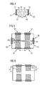
- FIG. 1 shows a main body 1 of length 1 and the width b.
- the main body 1 has the shape of a cuboid. He points two opposite side surfaces 41, 42 on. On each Side surface 41, 42 are each two outer electrodes 71, 72, 73, 74 arranged. On the side surface 41 are the outer electrodes 71, 73 arranged. On the side surface 42 are the External electrodes 72, 74 arranged. The outer electrodes will be applied by screen printing a metal-containing paste. Of the Base 1 extends with its largest dimension preferably in the longitudinal direction, indicated by the arrow is.
- FIG. 2 shows the component from FIG. 1 in a side view. In the direction of the arrow, the length d of the outer electrodes 71, 73 measured. The height of the component is s.
- FIG. 3 shows a longitudinal section through the component according to FIG. 2 parallel to the layer plane of an electrode layer. It comprises stacks of internal electrodes 31, 32, 33, 34, respectively lie one above the other. Each stack of internal electrodes 31, 32, 33, 34 is each with a common outer electrode 71, 72, 73, 74 electrically contacted. Any arrangement of internal electrodes 31, 32, 33, 34 together with the corresponding outer electrode 71, 72, 73, 74 forms a multilayer electrode 51, 52, 53, 54.
- Each side surface 41, 42 are the Outer electrodes of two multilayer electrodes 51, 53; 52, 54 arranged. Two multilayer electrodes 51, 52; 53, 54 are opposite each other in the device.
- lateral adjacent multilayer electrodes 51, 53 are in terms of all their electrically conductive components, for which the outer electrodes 51, 53 as well as all electrode layers 31, 33 count, spaced by a gap 83 from each other.
- the width of the gap 83 is denoted by f.
- FIG. 4 shows a section along the line C-C of FIG 3.
- the dielectric layers 2 are shown.
- the dielectric layers are stacked on top of each other.
- Between the dielectric layers 2 are internal electrodes 31, 32nd arranged.
- the device shown in Figure 4 can advantageously by laminating several dielectric layers, For example, ceramic green sheets, with internal electrodes 31 applied therebetween by screen printing, 32, followed by pressing and sintering of the film stack produced become. Subsequently, the outer electrodes 71, 72 applied to the base body 1.
- the internal electrodes 31, which belong to multilayer electrode 51 shown. They are in the form of a stack 61 on top of each other.
- the internal electrodes 32 which belong to the multilayer electrode 52, in Shape of a stack 62 one above the other.
- the internal electrodes 31, 32 are spaced apart by a gap 81 of width g.
- FIG. 5 shows a representation corresponding to Figure 3 with the Difference that another multilayer electrode 59 is provided is that a stack of superimposed internal electrodes 39 includes.
- the internal electrodes 39 extend from one End face 92 to the opposite end face 91 of the Body. They are each with common external electrodes 791, 792 electrically connected.
- the in Figure 5 illustrated geometry can be realized as a feedthrough component become.
- the internal electrodes 39 may be, for example be connected to a common ground terminal 791, 792, the all four multilayer electrodes 51, 52, 53, 54 in common is. It should be noted that the definition of width g is the same as in FIG. 3.
- FIG. 19 shows a variation of FIG Inner electrode 39 not only in the space between each other Internal electrodes 51, 52; 53, 54 arranged is, but is formed cross-shaped and also in the Interspace between each other in the longitudinal direction adjacent Internal electrodes 51 and 53 and 52 and 54, respectively.
- the others Inner electrode 39 may be connected to ground and acts as a shield for decoupling and reduces the Crosstalk.
- the further inner electrode 39 can each in the same electrode layer as the other internal electrodes 51, 52; 53, 54; 51, 53, 52 and 54 realized, or even in intermediate levels.
- FIG. 6 shows a further variation of the illustration from FIG 3.
- the internal electrodes 32, 34 have different lengths L1, L2.
- the capacity of multilayer capacitors can be varied become.
- FIG. 7 shows a further variation of FIG. 3, wherein eight Multi-layer electrodes are integrated in a basic body.
- FIG. 7 shows the multilayer electrodes 51, 52, 53, 54, 55, 56, 57, 58. They are formed of external electrodes 71, 72, 73, 74, 75, 76, 77, 78.
- the outer electrodes 72, 74, 76, 78 are located on the opposite side surface.
- Each two outer electrodes 71, 72; 73, 74; 75, 76; 77, 78 are each other arranged opposite.
- Two opposite each Outer electrodes and the two associated with them Multilayer electrodes form, for example, a multilayer capacitor.
- FIG. 8 shows a further variation of the illustration from FIG Figure 3, wherein the internal electrodes 31, 32, 33, 34 L-shaped are formed.
- the long legs of the L run respectively parallel to the axis connecting the two outer electrodes.
- g is the history of the column 81 in the longitudinal direction of the component prevail.
- FIG. 8 applies to the inequality described above the size ratios of the gap widths g and f.
- This version is the internal electrodes shown unshaded 31 and 33 connected to ground, so put Ground electrodes dar.
- the ground electrodes are between the hatched potential-carrying internal electrodes 32 and 34 arranged and shield these against each other. This improves the decoupling continues.
- FIG. 9 shows a variation of the embodiment of FIG 8, not four but eight multilayer electrodes and corresponding internal electrodes 31, 32, 33, 34, 35, 36, 37, 38, all of which are L-shaped, integrated in a basic body are.
- FIG. 10 shows a variation with respect to FIG arranged on a side surface of the body multilayer electrodes Internal electrodes 32, 34, 36, 38 in the form of a U and are connected to ground.
- the one on the opposite Side surface arranged internal electrodes 31, 33, 35, 37 are T-shaped.
- the arrangement of Internal electrodes 31, 32, 33, 34, 35, 36, 37, 38 to each other designed so that the middle leg of the T between the Leg of the U is arranged.
- the potential-carrying internal electrodes 31, 33, 35, 37th through the ground-connected U-shaped internal electrodes shielded against each other.
- the definition of the gap width g is again to be taken from Figure 10, wherein the gap width 81st between internal electrodes 31, 32 corresponding to FIG. 8 in FIG Is dimensioned longitudinal direction of the body.
- the T-shaped Internal electrodes 32, 34, 36, 38 can be depicted as in the figure have the same or different lengths.
- FIG. 11 shows a variation of the representation from FIG. 10, wherein the T-shaped internal electrodes 31, 32, 35, 37 with respect to the central portion of the T in different lengths L1, L2 are executed.
- the length of the legs of the U-shaped internal electrodes 32, 34, 36, 38 remain unchanged, are with Mass connected and thus ensure an unchanged good Shielding and decoupling of adjacent internal electrodes.
- FIG. 18 shows a variation of the illustrations from FIG. 8 and 10, wherein the potential-carrying internal electrodes to a common internal electrode 33 are united, the space between opposing internal electrodes almost completely fills.
- the potential-carrying T-shaped Internal electrodes 32, 34, 36 U-shaped and thus provides a good shielding and decoupling of the internal electrodes 32, 34, 36 for sure.
- FIG. 12 shows a variation of the representation from FIG. 4, wherein the internal electrodes 61, 62 are different from each other Have lengths L1, L2. According to FIG. 12, the width of the Gaps 81 between the multilayer electrodes 51, 52 by those internal electrodes 31, 32 that determine the lowest Distance from each other.
- FIG. 13 shows a variation of the illustration of FIG. 12; wherein the internal electrodes 31, 32 are greatly shortened, thus a very wide gap 81 between opposed multilayer electrodes arises.
- the gap 81 are more stacks 63, 64, 65 of superimposed internal electrodes 3 are arranged. This creates a series connection of several subcolumns, which allow the capacitance of the capacitors to further degrade.
- FIG. 14 shows a variation of the representation from FIG. 13, wherein the internal electrodes 3 of the stacks 63, 64, 65 to the internal electrodes the stack 61, 62 offset in height, ie in different layers of the stack are arranged. Thereby The capacity of the capacitor can be advantageous even further be reduced.
- FIG. 15 shows a variation of the detail B from FIG. 3, wherein the internal electrodes 31, 32 are concave. she each form at its ends two tips 102, 101; 103, 104.
- FIG. 16 shows a further variation to the detail B in FIG 3.
- the internal electrodes 31, 32 are convex.
- FIG. 17 shows a further variation of the detail B FIG. 3.
- the internal electrodes 31, 32 are in a middle region each provided with a tip 101 and 102, respectively.
- the invention is not limited to capacitors and varistors, but includes multilayer components of all kinds.
Abstract
Description
Die Erfindung betrifft ein elektrisches Vielschichtbauelement mit einem Grundkörper, enthaltend einen Stapel aus übereinanderliegenden Dielektrikumschichten mit dazwischenliegenden Elektrodenschichten.The invention relates to an electrical multilayer component with a base body containing a stack of superimposed Dielectric layers with intermediate layers Electrode layers.
Aus der Druckschrift DE 19931056A1 ist ein Vielschichtbauelement der eingangs genannten Art bekannt, bei dem auf gegenüberliegenden Seitenflächen des Grundkörpers angeordnete Elektrodenschichten zusammen mit den Dielektrikumschichten einen Vielschichtvaristor bilden. Die Elektrodenschichten überlappen einander nicht, wodurch der Vielschichtvaristor eine niedrige Kapazität aufweist.From the document DE 19931056A1 is a multilayer component of the type mentioned above, in which on opposite Side surfaces of the main body arranged Electrode layers together with the dielectric layers form a multilayer varistor. The electrode layers do not overlap each other, causing the multilayer varistor has a low capacity.
Das bekannte Bauelement hat den Nachteil, daß in einem einzigen Grundkörper nur eine einzige elektrische Funktion, nämlich die Funktion eines einzigen Varistors realisiert ist. Um auf einer Platine mit Hilfe des bekannten Bauelements eine Vielzahl von elektrischen Funktionen zu realisieren, ist es daher erforderlich, eine Vielzahl von Bauelementen, die einen entsprechend großen Platz auf der Platine beanspruchen, zu verwenden. Darüber hinaus steigt dadurch der Bestückungsaufwand in nachteiliger Weise.The known device has the disadvantage that in a single Basic body only a single electrical function, namely the function of a single varistor is realized. Around on a board with the help of the known device a It is to realize variety of electrical functions therefore required a variety of components, the one claim correspondingly large space on the board, too use. In addition, this increases the assembly costs disadvantageously.
Es ist daher Aufgabe der vorliegenden Erfindung, ein Bauelement der eingangs genannten Art anzugeben, bei dem mehrere elektrische Funktionen in einem einzigen Grundkörper realisiert sind.It is therefore an object of the present invention, a device specify the type mentioned, in which several realized electrical functions in a single body are.
Diese Aufgabe wird gelöst durch ein elektrisches Vielschichtbauelement gemäß dem Patentanspruch 1. Weitere Ausgestaltungen der Erfindung sind den abhängigen Patentansprüchen zu entnehmen. This object is achieved by an electrical multilayer component according to the patent claim 1. Further embodiments of the invention are entitled to the dependent claims remove.
Die Erfindung gibt ein integriertes elektrisches Vielschichtbauelement an, bei dem eine Mehrzahl einzelner Bauelemente mit minimierter parasitärer Kapazität und gleichzeitig minimierter Induktivität realisiert wird, indem zwischen Innenelektroden Spalte vorgesehen werden. Durch auf Masse gelegte abschirmende Innenelektroden wird auch das Übersprechverhalten bei hochfrequenten Signalen verbessert.The invention provides an integrated multilayer electrical component in which a plurality of individual components with minimized parasitic capacity and at the same time minimized Inductance is realized by placing between internal electrodes Be provided column. By grounded Shielding internal electrodes also becomes the crosstalk behavior improved at high frequency signals.
Es wird ein elektrisches Vielschichtbauelement angegeben, das einen Grundkörper aufweist. Der Grundkörper enthält einen Stapel aus übereinanderliegenden Dielektrikumschichten, zwischen denen Elektrodenschichten angeordnet sind, wobei der Stapel zumindest eine Elektrodenschicht umfasst.It is specified an electrical multilayer component, the has a main body. The main body contains one Stack of superimposed dielectric layers, between which electrode layers are arranged, wherein the Stack comprises at least one electrode layer.
Der Grundkörper weist zwei entlang der Stapelrichtung verlaufende, gegenüberliegende Seitenflächen auf. In jeder Elektrodenschicht sind Innenelektroden vorgesehen, die mit jeweils einer der Außenelektroden verbunden sind. Die Innenelektroden sind sich jeweils in der gleichen Elektrodenschicht mit einem Abstand g paarweise gegenüberstehend ausgebildet. Vielschichtelektroden werden aus den Innenelektroden gebildet, die in unterschiedlichen Elektrodenschichten ausgebildet und mit der gleichen Außenelektrode verbunden sind. Alle Innenelektroden einer Vielschichtelektrode überlappen einander. Im folgenden wird nur noch auf Vielschichtelektroden Bezug genommen, auch wenn diese im Grenzfall nur eine Innenelektrode umfassen.The main body has two running along the stacking direction, opposite side surfaces on. In every electrode layer internal electrodes are provided, each with one of the outer electrodes are connected. The internal electrodes are each in the same electrode layer with a Distance g formed in pairs opposite. Multilayer electrode are formed from the internal electrodes, which are in formed different electrode layers and with the same outer electrode are connected. All internal electrodes a multilayer electrode overlap each other. Hereinafter is only referred to multi-layer electrodes, too if in the limiting case they only comprise one inner electrode.
Bei erfindungsgemäßen Bauelementen sind dementsprechend die Vielschichtelektroden einander paarweise gegenüberstehend ausgebildet. Vielschichtelektroden, die mit unterschiedlichen Außenelektroden verbunden sind, sind lateral bzw. in Längsrichtung (quer zur Stapelrichtung und quer zur Achse, die die beiden einander zugeordneten Vielschichtelektroden verbindet) gegeneinander versetzt ausgebildet, durch einen Spalt beabstandet und überlappen sich nicht. In the case of components according to the invention, accordingly Multilayer electrodes facing each other in pairs educated. Multilayer electrodes with different External electrodes are connected, are lateral or in the longitudinal direction (transverse to the stacking direction and transverse to the axis, the connecting two mutually associated multilayer electrodes) formed offset from each other, spaced by a gap and do not overlap.
An jeder Seitenfläche sind jeweils mindestens zwei Außenelektroden angeordnet, die mit jeweils einer Vielschichtelektrode verbunden sind. Im Vielschichtbauelement sind so zumindest zwei jeweils zwei Vielschichtelektroden umfassende einzelne Bauelemente ausgebildet.There are at least two outer electrodes on each side surface arranged, each with a multilayer electrode are connected. In the multilayer component are so at least two each comprising two multilayer electrodes single Components designed.
Das Vielschichtbauelement hat den Vorteil, daß einander gegenüberliegende Vielschichtelektroden einander nicht überlappen. Dadurch gelingt es, aus zwei einander gegenüberliegenden Vielschichtelektroden einen Kondensator zu bilden, der eine sehr geringe Kapazität aufweist. Überraschend hat sich auch gezeigt, daß das Vielschichtbauelement eine gegenüber einem Einzelbauelement verringerte Induktivität aufweist. Dies wird auf die verminderte Länge der einander nicht überlappenden Innenelektroden zurückgeführt. Das Vielschichtbauelement bildet so ein Array einzelner unabhängig voneinander zu betreibender Einzelbauelemente aus, zwischen denen nur geringes Übersprechen statt findet. Kapazitive und andere Kopplungen zwischen den einzelnen Bauelementen des erfindungsgemäßen Vielschichtbauelements sind minimiert. Das Vielschichtbauelement kann auch einem anderen Bauelementtyp zugehörig sein und kann beispielsweise als Vielschichtvaristor ausgebildet sein.The multilayer component has the advantage that opposing one another Multilayer electrodes do not overlap each other. This succeeds, from two opposite ones Multilayer electrodes to form a capacitor, the one has very low capacity. Surprisingly, too shown that the multilayer component one compared to a Single component has reduced inductance. this will on the reduced length of each other not overlapping Internal electrodes returned. The multilayer component forms such an array of individual independently operated Single components from, between which only small Crosstalk takes place. Capacitive and other couplings between the individual components of the invention Multi-layer component are minimized. The multilayer component may also be associated with another type of component and For example, it can be designed as a multilayer varistor.
Die Realisierung von Kondensatoren mit einer kontrollierten, sehr kleinen Kapazität in klassischer Vielschichtbauweise, bei der die Innenelektroden einander überlappen, ist schwierig, da die Kapazität solcher Vielschichtkondensatoren sehr stark von der gegenseitigen Justage der Elektrodenschichten abhängt. Somit gehen Justierfehler beim Aufdrucken der Innenelektroden auf die Dielektrikumschichten sehr stark in die Kapazität ein, was im allgemeinen zu Kapazitäten führt, die größer sind als die gewünschte Kapazität.The realization of capacitors with a controlled, very small capacity in classic multilayer construction, where the internal electrodes overlap each other is difficult because the capacity of such multilayer capacitors is very high strong from the mutual adjustment of the electrode layers depends. Thus, adjustment errors occur when printing the internal electrodes on the dielectric layers very strong in the Capacity, which generally leads to capacity, the are larger than the desired capacity.
Das Vielschichtbauelement hat des weiteren den Vorteil, daß zumindest vier Vielschichtelektroden in dem Grundkörper angeordnet sind. Dadurch gelingt es, in das Vielschichtbauelement eine aus einer Vielzahl elektrischer Funktionen zu integrieren. Je nachdem, welches Material für die Dielektrikumschichten gewählt wird, kann beispielsweise die Anordnung von zumindest zwei Vielschichtvaristoren oder von zumindest zwei Vielschichtkondensatoren mit einem einzigen Vielschichtbauelement realisiert werden.The multilayer component further has the advantage that at least four multilayer electrodes arranged in the base body are. This makes it possible in the multilayer component to integrate one of a variety of electrical functions. Depending on which material for the dielectric layers is selected, for example, the arrangement of at least two multilayer varistors or at least two Multilayer capacitors with a single multilayer component will be realized.
Es ist darüber hinaus auch denkbar, für ein Paar von gegenüberliegenden Vielschichtelektroden eine Kondensatorkeramik zu verwenden, während für das andere Paar von gegenüberliegenden Vielschichtelektroden eine Varistorkeramik verwendet wird. Somit gelingt die Integration eines Vielschichtvaristors und eines Vielschichtkondensators, jeweils mit sehr geringer Kapazität, in ein einziges Bauelement.It is also conceivable for a pair of opposite Multilayer electrodes a capacitor ceramic to use while opposite for the other pair Multilayer electrodes used a varistor ceramic becomes. Thus, the integration of a multilayer varistor succeeds and a multilayer capacitor, each with very little Capacity, in a single component.
Es ist ein Vielschichtbauelement vorteilhaft, bei dem elektrisch leitende Bestandteile von nebeneinander liegenden Vielschichtelektroden durch einen Spalt voneinander beabstandet sind. Dieser Spalt hat die Breite f. Darüber hinaus ist es vorteilhaft, wenn elektrisch leitende Bestandteile von einander gegenüberliegenden Vielschichtelektroden durch einen Spalt der Breite g voneinander beabstandet sind. Dabei gilt: f ≥ 1,3 g, besser f ≥ 1,3 g. Durch das Einhalten der beschriebenen Abstandsregeln kann beispielsweise ein Übersprechen zwischen nebeneinanderliegenden Kondensatoren vermindert werden. Von Vorteil sind auch Bauelemente, bei den f ≥ 1,5 g. Damit kann die Entkopplung weiter verbessert werden.It is advantageous for a multilayer component in which electrical conductive components of juxtaposed Multi-layer electrodes spaced from each other by a gap are. This gap has the width f. In addition, it is it is advantageous if electrically conductive components of opposite multilayer electrodes by a Gap of width g are spaced from each other. Where: f ≥ 1.3 g, better f ≥ 1.3 g. By observing the described Distance rules can be, for example, crosstalk reduced between adjacent capacitors become. Also advantageous are components in which f ≥ 1.5 g. Thus, the decoupling can be further improved.
Indem also der Abstand der elektrisch leitenden Bestandteile von nebeneinanderliegenden Vielschichtelektroden größer ausgelegt ist als der Abstand der elektrisch leitenden Bestandteile von einander gegenüberliegenden Elektroden, kann eine Entkopplung erreicht werden zwischen normalerweise zu ein und demselben elektrischen Bauelement gehörenden gegenüberliegenden Vielschichtelektroden und den zu einem davon verschiedenen elektrischen Bauelement gehörenden danebenliegenden Vielschichtelektroden. So by the distance between the electrically conductive components designed by juxtaposed multilayer electrodes larger is the distance of the electrically conductive components from opposite electrodes, one can Decoupling can be achieved between normally to and belonging to the same electrical component opposite Multilayer electrodes and the one to another electrical component belonging adjacent multilayer electrodes.
In diesem Zusammenhang ist unter einem Spalt ein Abschnitt im Grundkörper zu verstehen, der frei von Elektrodenmaterial, also von elektrisch leitendem Material ist. Der Spalt ist nicht notwendigerweise mit Luft gefüllt, sondern kann auch durch Material der Dielektrikumschichten gefüllt sein.In this context, under a gap is a section in Basic body understood to be free of electrode material, So is of electrically conductive material. The gap is not necessarily filled with air, but also can be filled by material of the dielectric layers.
Es kann in einer anderen Ausführungsform eine weitere Vielschichtelektrode vorgesehen sein, deren Innenelektroden im Spalt zwischen gegenüberliegenden Vielschichtelektroden verlaufen und deren Außenelektrode an der Stirnfläche des Grundkörpers angeordnet sind. Auf diese Art und Weise läßt sich ein Durchführungsbauelement realisieren, bei dem beispielsweise vier an den Seitenflächen angeordnete Vielschichtelektroden eine gemeinsame Massenelektrode haben, die an einer der Stirnflächen oder auch an beiden Stirnflächen des Grundkörpers aus dem Grundkörper herausgeführt ist. Dadurch lassen sich in vorteilhafter Weise besonders kompakte Schaltungsvarianten auf Platinen realisieren.It may be another multilayer electrode in another embodiment be provided, whose internal electrodes in Gap between opposite multilayer electrodes and its outer electrode on the end face of the main body are arranged. In this way can be implement a feedthrough component, in which, for example four multi-layer electrodes arranged on the side surfaces have a common ground electrode connected to a the end faces or at both end faces of the body is led out of the body. Leave it advantageously particularly compact circuit variants realize on boards.
Des weiteren ergibt sich aus dieser Ausführungsform der Vorteil, daß mit Hilfe von stirnflächenseitig aus dem Grundkörper herausgeführten Vielschichtelektroden eine interne Verschaltung mehrerer Vielschichtelektroden realisiert werden kann. Dadurch reduziert sich der später mit dem Vielschichtbauelement zu bestückenden Platine der Verschaltungs- und Verdrahtungsaufwand, was zusätzlich Platz auf der Platine einspart.Furthermore, this embodiment provides the advantage that with the help of end face side of the body led out multilayer electrodes an internal interconnection several multilayer electrodes are realized can. This reduces the later with the multilayer component to be assembled and interconnected board Wiring effort, which in addition space on the board saves.
In einer weiteren Ausführungsform ist ein Vielschichtbauelement vorgesehen, dessen Vielschichtelektroden unterschiedliche Anzahlen von Elektrodenschichten bzw. Innenelektroden aufweisen. Dadurch gelingt es, Kondensatoren bzw. Varistoren in das Vielschichtbauelement zu integrieren, deren Kapazität voneinander verschieden ist, was die mit dem Vielschichtbauelement erzielbare Variationsbreite erhöht. In a further embodiment, a multilayer component is provided, whose multilayer electrodes different Number of electrode layers or internal electrodes exhibit. This makes it possible, capacitors or varistors to integrate into the multilayer component whose capacity different from each other, what with the multilayer component achievable range of variation increased.
In einer anderen Ausführungsform sind Vielschichtelektroden vorgesehen, deren Innenelektroden im Vielschichtbauelement unterschiedliche Flächen aufweisen. Auch dadurch gelingt die Integration einer großen Bauelementevielfalt in das Vielschichtbauelement.In another embodiment, multilayer electrodes provided, the internal electrodes in the multilayer component have different areas. This also succeeds Integration of a large variety of components in the multilayer component.
Des weiteren kann die Vielfalt des Bauelements erhöht werden, indem Elektrodenschichten vorgesehen sind, deren Länge voneinander verschieden ist.Furthermore, the diversity of the device can be increased by electrode layers are provided whose length from each other is different.
In einer anderen Ausführungsform des Vielschicht-Bauelements sind im Grundkörper Dielektrikumschichten vorhanden, deren Dielektrizitätskonstante voneinander verschieden ist. Auch dadurch kann die Bauelementevielfalt erhöht werden.In another embodiment of the multilayer component Dielectric layers are present in the main body whose Dielectric constant is different from each other. Also thereby, the component diversity can be increased.
In einer weiteren Ausführungsform des Vielschichtbauelements enthalten die Dielektrikumschichten ein Keramikmaterial mit Varistoreffekt. In Betracht kommen beispielsweise Keramikmaterialien, die ZnO-Bi oder ZnO-Pr enthalten. Solche Dielektrikumschichten haben den Vorteil, daß sie neben dem Kondensator noch als weiteres Bauelement einen Varistor in das Vielschichtbauelement integrieren.In a further embodiment of the multilayer component The dielectric layers contain a ceramic material Varistor. For example, ceramic materials may be considered containing ZnO-Bi or ZnO-Pr. Such dielectric layers have the advantage of being next to the capacitor even as another component a varistor in the Integrate multilayer component.
In einer anderen Ausführungsform des Vielschichtbauelements können die Dielektrikumschichten eine Kondensatorkeramik auf der Basis von Bariumtitanat enthalten. Als Dielektrikumschicht kommt beispielsweise eine sogenannte "C0G"-Keramik in Betracht. Es kommt aber auch eine "X7R"-Keramik in Betracht, beispielsweise dotiertes Bariumtitanat. In einer weiteren Ausführungsform des Vielschichtbauelements sind Elektrodenschichten vorgesehen, die an den Innenseiten konkav oder konvex ausgeformt sind.In another embodiment of the multilayer component For example, the dielectric layers may have a capacitor ceramic contain the base of barium titanate. As a dielectric layer For example, a so-called "C0G" ceramic comes in Consideration. But it is also a "X7R" ceramic into consideration, for example, doped barium titanate. In another Embodiment of the multilayer component are electrode layers provided, on the insides concave or convex are formed.
In einer weiteren Ausführungsform des Vielschicht-Bauelements sind Innenelektroden vorgesehen, die Spitzen aufweisen, wobei die Spitzen einander zugeordneter Vielschichtelektroden zueinander weisen. In a further embodiment of the multilayer component internal electrodes are provided which have tips, wherein the tips of mutually associated multilayer electrodes to each other point.
In einer weiteren Ausführungsform des Vielschicht-Bauelements sind in einem Spalt Stapel von übereinanderliegenden Elektrodenschichten angeordnet. Dadurch kann gewissermaßen die Anzahl der Spalte zwischen zwei Vielschichtelektroden durch Einfügen weiterer Innenelektroden erhöht werden. Durch eine solche serielle Anordnung mehrerer Spalte kann die Kapazität eines Vielschichtkondensators weiter reduziert werden.In a further embodiment of the multilayer component are in a gap stack of superimposed electrode layers arranged. This can effectively reduce the number the gap between two multilayer electrodes Insertion of additional internal electrodes can be increased. By a such serial arrangement of multiple column, the capacity a multilayer capacitor can be further reduced.
In einer anderen Ausführungsform des Vielschicht-Bauelements können die Elektrodenschichten eines in einem Spalt angeordneten Stapels versetzt zu den Innenelektroden einer Vielschichtelektrode angeordnet sein. Dadurch gelingt eine weitere Reduzierung der Kapazität.In another embodiment of the multilayer component For example, the electrode layers may be arranged in a gap Stack offset to the inner electrodes of a multilayer electrode be arranged. This succeeds another Reduction of capacity.
Der Grundkörper des Vielschichtbauelements kann ein Grundkörper sein, dessen Grundfläche kleiner als 5,2 mm2 beträgt. Dann enthält das Vielschichtbauelement mindestens vier Vielschichtelektroden.The base body of the multilayer component may be a base body whose base area is less than 5.2 mm 2 . Then, the multilayer component contains at least four multilayer electrodes.
Es ist darüber hinaus auch möglich, die Grundfläche des Grundkörpers so auszubilden, daß sie kleiner als 8 mm2 ist. Dann können mindestens vier Vielschichtelektroden in dem Grundkörper enthalten sein.It is also possible, the base of the body in such a way that it is smaller than 8 mm 2 . Then at least four multilayer electrodes can be contained in the main body.
In einer anderen Ausführungsform des Vielschichtbauelements können die Elektrodenschichten beispielsweise aus Silber, Palladium, Platin oder auch aus einer Legierung aus Silber und Platin bzw. aus Silber und Palladium bestehen bzw. solche Metalle bzw. Legierungen enthalten. Die Elektrodenschichten können aber auch aus Kupfer oder Nickel bestehen bzw. Kupfer oder Nickel enthalten.In another embodiment of the multilayer component For example, the electrode layers may be made of silver, Palladium, platinum or even an alloy of silver and platinum or of silver and palladium or such Contain metals or alloys. The electrode layers but can also consist of copper or nickel or copper or nickel.
In einer weiteren Ausführungsform des Vielschichtbauelements sind Innenelektroden L-förmig ausgebildet. In a further embodiment of the multilayer component internal electrodes are L-shaped.
In einer weiteren Ausführungsform des Vielschichtbauelements sind Innenelektroden T-förmig ausgebildet.In a further embodiment of the multilayer component internal electrodes are T-shaped.
In einer weiteren Ausführungsform des Vielschichtbauelements sind Innenelektroden U-förmig ausgebildet.In a further embodiment of the multilayer component internal electrodes are U-shaped.
Im Folgenden wird die Erfindung anhand von Ausführungsbeispielen und den dazugehörigen Figuren näher erläutert.
- Figur 1
- zeigt beispielhaft ein Vielschichtbauelement in einer Draufsicht.
- Figur 2
- zeigt das Vielschichtbauelement aus Figur 1 in einer Seitenansicht.
Figur 3- zeigt das Vielschichtbauelement aus Figur 1 in einem Längsschnitt.
- Figur 4
- zeigt den Schnitt entlang der Linie C-C aus Figur 3.
- Figur 5
- zeigt eine Darstellung eines Bauelements gemäß Figur 3 mit dem Unterschied, daß eine weitere Vielschichtelektrode in der Mitte vorgesehen ist.
- Figur 6
- zeigt eine Darstellung eines Bauelements entsprechend Figur 3 mit dem Unterschied, daß Elektrodenschichten unterschiedliche Längen aufweisen.
- Figur 7
- zeigt eine Darstellung eines Bauelements entsprechend Figur 3 mit dem Unterschied, daß acht Vielschichtelektroden integriert sind.
- Figur 8
- zeigt eine Darstellung entsprechend Figur 3 mit dem Unterschied, daß Elektrodenschichten L-förmig ausgebildet sind.
Figur 9- zeigt eine Darstellung entsprechend Figur 8 mit dem Unterschied, daß acht anstelle von vier Vielschichtelektroden integriert sind.
- Figur 10
- zeigt eine Darstellung entsprechend Figur 9 mit dem
Unterschied, daß Elektrodenschichten U-förmig bzw.
T-förmig ausgebildet sind. - Figur 11
- zeigt eine Darstellung entsprechend Figur 10 mit dem Unterschied, daß Elektrodenschichten unterschiedliche Längen aufweisen.
- Figur 12
- zeigt einen Querschnitt entsprechend Figur 4 mit dem Unterschied, daß die Innenelektroden unterschiedliche Längen aufweisen.
- Figur 13
- zeigt einen Querschnitt entsprechend Figur 4 mit dem Unterschied, daß im Spalt weitere Innenelektroden angeordnet sind.
- Figur 14
- zeigt eine Darstellung entsprechend Figur 13 mit dem Unterschied, daß die im Spalt angeordneten Innenelektroden zu den Innenelektroden der Vielschichtelektroden in der Höhe versetzt sind.
- Die Figuren 15, 16 und 17
- zeigen für den Ausschnitt
B aus Figur 3 weitere Ausführungsformen. - Figur 18
- zeigt ein Vielschichtbauelement mit einer gemeinsamen Masseelektrode in einem Längsschnitt.
- Figur 19
- zeigt ein weiteres Vielschichtbauelement mit einer gemeinsamen Masseelektrode in einem Längsschnitt.
- FIG. 1
- shows by way of example a multilayer component in a plan view.
- FIG. 2
- shows the multilayer component of Figure 1 in a side view.
- FIG. 3
- shows the multilayer component of Figure 1 in a longitudinal section.
- FIG. 4
- shows the section along the line CC of Figure 3.
- FIG. 5
- shows a representation of a device according to Figure 3 with the difference that a further multilayer electrode is provided in the middle.
- FIG. 6
- shows a representation of a device according to Figure 3 with the difference that electrode layers have different lengths.
- FIG. 7
- shows a representation of a device according to Figure 3 with the difference that eight multilayer electrodes are integrated.
- FIG. 8
- shows a representation corresponding to Figure 3 with the difference that electrode layers are L-shaped.
- FIG. 9
- shows a representation corresponding to Figure 8 with the difference that eight instead of four multilayer electrodes are integrated.
- FIG. 10
- shows a representation corresponding to Figure 9 with the difference that electrode layers U-shaped or
T-shaped. - FIG. 11
- shows a representation according to Figure 10 with the difference that electrode layers have different lengths.
- FIG. 12
- shows a cross section corresponding to Figure 4 with the difference that the internal electrodes have different lengths.
- FIG. 13
- shows a cross section corresponding to Figure 4 with the difference that more internal electrodes are arranged in the gap.
- FIG. 14
- shows a view corresponding to Figure 13 with the difference that the internal electrodes arranged in the gap are offset in height to the inner electrodes of the multilayer electrodes.
- FIGS. 15, 16 and 17
- show for the detail B of Figure 3 further embodiments.
- FIG. 18
- shows a multilayer component with a common ground electrode in a longitudinal section.
- FIG. 19
- shows a further multilayer component with a common ground electrode in a longitudinal section.
Figur 1 zeigt einen Grundkörper 1 der Länge 1 und der Breite
b. Der Grundkörper 1 hat die Form eines Quaders. Er weist
zwei gegenüberliegende Seitenflächen 41, 42 auf. Auf jeder
Seitenfläche 41, 42 sind jeweils zwei Außenelektroden 71, 72,
73, 74 angeordnet. Auf der Seitenfläche 41 sind die Außenelektroden
71, 73 angeordnet. Auf der Seitenfläche 42 sind die
Außenelektroden 72, 74 angeordnet. Die Außenelektroden werden
durch Siebdrucken einer metallhaltigen Paste aufgebracht. Der
Grundkörper 1 erstreckt sich mit seiner größten Ausdehnung
vorzugsweise in Längsrichtung, die durch den Pfeil angedeutet
ist.FIG. 1 shows a main body 1 of length 1 and the width
b. The main body 1 has the shape of a cuboid. He points
two opposite side surfaces 41, 42 on. On each
Figur 2 zeigt das Bauelement aus Figur 1 in einer Seitenansicht.
In Pfeilrichtung ist die Länge d der Außenelektroden
71, 73 gemessen. Die Höhe des Bauelements ist s.FIG. 2 shows the component from FIG. 1 in a side view.
In the direction of the arrow, the length d of the
Figur 3 zeigt einen Längsschnitt durch das Bauelement gemäß
Figur 2 parallel zur Schichtebene einer Elektrodenschicht. Es
umfaßt Stapel von Innenelektroden 31, 32, 33, 34, die jeweils
übereinander liegen. Jeder Stapel von Innenelektroden 31, 32,
33, 34 ist mit jeweils einer gemeinsamen Außenelektrode 71,
72, 73, 74 elektrisch kontaktiert. Jede Anordnung von Innenelektroden
31, 32, 33, 34 zusammen mit der entsprechenden Auβenelektrode
71, 72, 73, 74 bildet eine Vielschichtelektrode
51, 52, 53, 54. Entlang jeder Seitenfläche 41, 42 sind die
Außenelektroden von jeweils zwei Vielschichtelektroden 51,
53; 52, 54 angeordnet. Jeweils zwei Vielschichtelektroden 51,
52; 53, 54 liegen einander im Bauelement gegenüber. Lateral
nebeneinander liegende Vielschichtelektroden 51, 53 sind hinsichtlich
ihrer sämtlichen elektrisch leitenden Bestandteile,
wozu die Außenelektroden 51, 53 sowie sämtliche Elektrodenschichten
31, 33 zählen, durch einen Spalt 83 voneinander beabstandet.
Die Breite des Spaltes 83 ist mit f bezeichnet.FIG. 3 shows a longitudinal section through the component according to FIG
FIG. 2 parallel to the layer plane of an electrode layer. It
comprises stacks of
Hinsichtlich ihrer Innenelektroden 31, 33 sind die Vielschichtelektroden
51, 53 unterschiedlicher Paare lateral
durch den Spalt 82 voneinander beabstandet. Auch einander gegenüberliegende
Vielschichtelektroden 53, 54 jeweils eines
Paares sind durch Spalte 81, 84 voneinander beabstandet. Die
Spalte 81, 84 müssen nicht notwendigerweise dieselbe Breite g
aufweisen. In der in Figur 3 gezeigten Anordnung betrifft die
Beabstandung einander gegenüberliegender Vielschichtelektroden
53, 54; 51, 52 gleichzeitig die Beabstandung hinsichtlich
ihrer Innenelektroden 34, 33; 32, 31. In Figur 3 ist noch ein
Ausschnitt in Form eines gestrichelten Rechtecks mit B gekennzeichnet,
welcher in weiteren Figuren in anderen Variationen
gezeigt ist.With regard to their
Figur 4 zeigt einen Schnitt entlang der Linie C-C aus Figur
3. In Figur 4 sind die Dielektrikumschichten 2 dargestellt.
Die Dielektrikumschichten sind übereinandergestapelt. Zwischen
den Dielektrikumschichten 2 sind Innenelektroden 31, 32
angeordnet. Das in Figur 4 gezeigte Bauelement kann vorteilhafterweise
durch Übereinanderlaminieren von mehreren Dielektrikumschichten,
beispielsweise keramische Grünfolien, mit
dazwischen durch Siebdruck aufgebrachte Innenelektroden 31,
32, anschließendes Pressen und Sintern des Folienstapels hergestellt
werden. Anschließend werden die Außenelektroden 71,
72 auf den Grundkörper 1 aufgebracht. In Figur 4 sind die Innenelektroden
31, die zur Vielschichtelektrode 51 gehören,
dargestellt. Sie liegen in Form eines Stapels 61 übereinander.
Ebenfalls in gleicher Art und Weise liegen die Innenelektroden
32, die zur Vielschichtelektrode 52 gehören, in
Form eines Stapels 62 übereinander. Die Innenelektroden 31,
32 sind durch einen Spalt 81 mit der Breite g voneinander beabstandet.FIG. 4 shows a section along the line C-C of FIG
3. In Figure 4, the dielectric layers 2 are shown.
The dielectric layers are stacked on top of each other. Between
the dielectric layers 2 are
Figur 5 zeigt eine Darstellung entsprechend Figur 3 mit dem
Unterschied, daß eine weitere Vielschichtelektrode 59 vorgesehen
ist, die einen Stapel von übereinanderliegenden Innenelektroden
39 umfaßt. Die Innenelektroden 39 verlaufen von einer
Stirnfläche 92 zur gegenüberliegenden Stirnfläche 91 des
Grundkörpers. Sie sind jeweils mit gemeinsamen Außenelektroden
791, 792 elektrisch leitend verbunden. Die in Figur 5
dargestellte Geometrie kann als Durchführungsbauelement realisiert
werden. Die Innenelektroden 39 können beispielsweise
mit einem gemeinsamen Masseanschluß 791, 792 verbunden werden,
der allen vier Vielschichtelektroden 51, 52, 53, 54 gemeinsam
ist. Es ist zu beachten, daß die Definition der Breite
g dieselbe ist wie in Figur 3.Figure 5 shows a representation corresponding to Figure 3 with the
Difference that another
Figur 19 zeigt eine Variation von Figur 5, bei der die weitere
Innenelektrode 39 nicht nur im Raum zwischen einander gegenüberliegenden
Innenelektroden 51, 52; 53, 54 angeordnet
ist, sondern kreuzförmig ausgebildet ist und sich auch in den
Zwischenraum zwischen einander in Längsrichtung benachbarten
Innenelektroden 51 und 53 bzw. 52 und 54 erstreckt. Die weitere
Innenelektrode 39 kann mit Masse verbunden sein und
wirkt so als Abschirmung zur Entkopplung und vermindert das
Übersprechen. Die weitere Innenelektrode 39 kann jeweils in
der gleichen Elektrodenschicht wie die übrigen Innenelektroden
51, 52; 53, 54; 51, 53, 52 und 54 realisiert sein, oder
auch in dazwischenliegenden Ebenen.FIG. 19 shows a variation of
Figur 6 zeigt eine weitere Variation der Darstellung aus Figur
3. In Figur 6 ist deutlich zu erkennen, daß die Innenelektroden
32, 34 unterschiedliche Längen L1, L2 aufweisen.
Dadurch kann die Kapazität von Vielschichtkondensatoren variiert
werden.FIG. 6 shows a further variation of the illustration from FIG
3. In Figure 6 it can be clearly seen that the
Figur 7 zeigt eine weitere Variation von Figur 3, wobei acht
Vielschichtelektroden in einem Grundkörper integriert sind.
In Figur 7 sind dargestellt die Vielschichtelektroden 51, 52,
53, 54, 55, 56, 57, 58. Sie sind gebildet aus Außenelektroden
71, 72, 73, 74, 75, 76, 77, 78. Dabei befinden sich die Auβenelektroden
71, 73, 75, 77 auf ein und derselben Seitenfläche
des Grundkörpers. Die Außenelektroden 72, 74, 76, 78 befinden
sich auf der gegenüberliegenden Seitenfläche. Jeweils
zwei Außenelektroden 71, 72; 73, 74; 75, 76; 77, 78 sind einander
gegenüberliegend angeordnet. Jeweils zwei gegenüberliegende
Außenelektroden und die mit ihnen verbunbenen zwei
Vielschichtelektroden bilden dabei beispielsweise einen Vielschichtkondensator. FIG. 7 shows a further variation of FIG. 3, wherein eight
Multi-layer electrodes are integrated in a basic body.
FIG. 7 shows the
Figur 8 zeigt eine weitere Variation der Darstellung aus der
Figur 3, wobei die Innenelektroden 31, 32, 33, 34 L-förmig
ausgebildet sind. Die langen Schenkel des L verlaufen jeweils
parallel zu der die beiden Außenelektroden verbindenden Achse.
Für die Definition der Werte g ist der Verlauf der Spalte
81 in Längsrichtung des Bauelements maßgebend. Auch im Fall,
der Figur 8 gilt die weiter oben beschriebene Ungleichung betreffend
die Größenverhältnisse der Spaltbreiten g und f. In
dieser Ausführung sind die unschraffiert dargestellten Innenelektroden
31 und 33 mit Masse verbunden, stellen also
Masseelektroden dar. Die Masseelektroden sind zwischen den
schraffierten potentialführenden Innenelektroden 32 und 34
angeordnet und schirmen diese gegeneinander ab. Dies verbessert
die Entkopplung weiter.FIG. 8 shows a further variation of the illustration from FIG
Figure 3, wherein the
Figur 9 zeigt eine Variation des Ausführungsbeispiels aus Figur
8, wobei nicht vier sondern acht Vielschichtelektroden
und entsprechende Innenelektroden 31, 32, 33, 34, 35, 36, 37,
38, die allesamt L-förmig sind, in einem Grundkörper integriert
sind.FIG. 9 shows a variation of the embodiment of FIG
8, not four but eight multilayer electrodes
and corresponding
Figur 10 zeigt eine Variation gegenüber Figur 9, bei der die
auf einer Seitenfläche des Grundkörpers angeordneten Vielschichtelektroden
Innenelektroden 32, 34, 36, 38 in Form eines
U aufweisen und mit Masse verbunden sind. Die auf der gegenüberliegenden
Seitenfläche angeordneten Innenelektroden
31, 33, 35, 37 sind T-förmig ausgebildet. Die Anordnung der
Innenelektroden 31, 32, 33, 34, 35, 36, 37, 38 zueinander ist
so ausgeführt, daß der mittlere Schenkel des T zwischen den
Schenkel des U angeordnet ist. Auch bei dieser Ausführung
sind die Potential führenden Innenelektroden 31, 33, 35, 37
durch die mit Masse verbundenen U-förmigen Innenelektroden
gegeneinander abgeschirmt. Die Definition der Spaltbreite g
ist wiederum Figur 10 zu entnehmen, wobei die Spaltbreite 81
zwischen Innenelektroden 31, 32 entsprechend Figur 8 in
Längsrichtung des Grundkörpers bemessen wird. Die T-förmigen
Innenelektroden 32, 34, 36, 38 können wie in der Figur abgebildet
gleiche oder auch unterschiedliche Längen aufweisen.FIG. 10 shows a variation with respect to FIG
arranged on a side surface of the body multilayer electrodes
Figur 11 zeigt eine Variation der Darstellung aus Figur 10,
wobei die T-förmigen Innenelektroden 31, 32, 35, 37 bezüglich
des Mittelabschnitts des T in unterschiedlicher Länge L1, L2
ausgeführt sind. Die Länge der Schenkel der U-förmigen Innenelektroden
32, 34, 36, 38 bleiben unverändert, sind mit
Masse verbunden und gewährleisten so eine unverändert gute
Abschirmung und Entkopplung benachbarter Innenelektroden.FIG. 11 shows a variation of the representation from FIG. 10,
wherein the T-shaped
Figur 18 zeigt eine Variation der Darstellungen aus Figur 8
und 10, wobei die potentialführenden Innenelektroden zu einer
gemeinsamen Innenelektrode 33 vereinigt sind, die den Raum
zwischen gegenüber liegenden Innenelektroden nahezu vollständig
ausfüllt. Wie bei der Ausführung nach Figur 10 umschließt
die gemeinsame Innenelektrode 33 die potentialführenden T-förmigen
Innenelektroden 32, 34, 36 U-förmig und stellt somit
eine gute Abschirmung und Entkopplung der Innenelektroden 32,
34, 36 sicher.FIG. 18 shows a variation of the illustrations from FIG. 8
and 10, wherein the potential-carrying internal electrodes to a
common
Figur 12 zeigt eine Variation der Darstellung aus Figur 4,
wobei die Innenelektroden 61, 62 voneinander verschiedene
Längen L1, L2 aufweisen. Gemäß Figur 12 ist die Breite des
Spalts 81 zwischen den Vielschichtelektroden 51, 52 durch
diejenigen Innenelektroden 31, 32 bestimmt, die den geringsten
Abstand voneinander aufweisen.FIG. 12 shows a variation of the representation from FIG. 4,
wherein the
Figur 13 zeigt eine Variation der Darstellung von Figur 12,
wobei die Innenelektroden 31, 32 stark verkürzt sind, womit
ein sehr breiter Spalt 81 zwischen gegenüberliegenden Vielschichtelektroden
entsteht. Im Spalt 81 sind weitere Stapel
63, 64, 65 von übereinanderliegenden Innenelektroden 3 angeordnet.
Dadurch entsteht eine Serienschaltung mehrerer Subspalte,
die es ermöglichen, die Kapazität der Kondensatoren
noch weiter zu erniedrigen. FIG. 13 shows a variation of the illustration of FIG. 12;
wherein the
Figur 14 zeigt eine Variation der Darstellung aus Figur 13,
wobei die Innenelektroden 3 der Stapel 63, 64, 65 zu den Innenelektroden
der Stapel 61, 62 in der Höhe versetzt, also in
verschiedenen Schichten des Stapels angeordnet sind. Dadurch
kann die Kapazität des Kondensators vorteilhaft noch weiter
verringert werden.FIG. 14 shows a variation of the representation from FIG. 13,
wherein the
Figur 15 zeigt eine Variation des Ausschnitts B aus Figur 3,
wobei die Innenelektroden 31, 32 konkav ausgebildet sind. Sie
bilden dabei an ihren Enden jeweils zwei Spitzen 102, 101;
103, 104.FIG. 15 shows a variation of the detail B from FIG. 3,
wherein the
Figur 16 zeigt eine weitere Variation zum Ausschnitt B in Figur
3. Hier sind die Innenelektroden 31, 32 konvex ausgebildet.FIG. 16 shows a further variation to the detail B in FIG
3. Here, the
Figur 17 zeigt eine weitere Variation des Ausschnitts B aus
Figur 3. Hier sind die Innenelektroden 31, 32 in einem Mittelbereich
jeweils mit einer Spitze 101 bzw. 102 versehen.FIG. 17 shows a further variation of the detail B
FIG. 3. Here, the
Die Erfindung beschränkt sich nicht auf Kondensatoren und Varistoren, sondern umfasst Vielschichtbauelemente aller Art. The invention is not limited to capacitors and varistors, but includes multilayer components of all kinds.
Bezugszeichenliste
- 1
- Grundkörper
- 2
- Dielektrikumschicht
- 3, 31, 32, 33, 34, 35, 36, 37, 38, 39
- Elektrodenschicht
- 41, 42
- Seitenfläche
- 51, 52, 53, 54, 55, 56, 57, 58, 59
- Vielschichtelektrode
- 61, 62, 63, 64, 65 71, 72, 73, 74, 75,
- Stapel
- 76, 77, 78, 791, 792
- Außenelektrode
- 81, 82, 83, 84
- Spalt
- 91, 92
- Stirnfläche
- 101, 102, 103, 104
- Spitze
- A
- Grundfläche
- L1, L2, L3, L4
- Länge
- B
- Ausschnitt
- 1
- Länge
- b
- Breite
- d
- Länge
- s
- Höhe
- g, f
- Breite
- 1
- body
- 2
- dielectric
- 3, 31, 32, 33, 34, 35, 36, 37, 38, 39
- electrode layer
- 41, 42
- side surface
- 51, 52, 53, 54, 55, 56, 57, 58, 59
- Multilayer electrode
- 61, 62, 63, 64, 65 71, 72, 73, 74, 75,
- stack
- 76, 77, 78, 791, 792
- outer electrode
- 81, 82, 83, 84
- gap
- 91, 92
- face
- 101, 102, 103, 104
- top
- A
- Floor space
- L1, L2, L3, L4
- length
- B
- neckline
- 1
- length
- b
- width
- d
- length
- s
- height
- g, f
- width
Claims (19)
Applications Claiming Priority (2)
| Application Number | Priority Date | Filing Date | Title |
|---|---|---|---|
| DE2002135011 DE10235011A1 (en) | 2002-07-31 | 2002-07-31 | Electrical multilayer component |
| DE10235011 | 2002-07-31 |
Publications (2)
| Publication Number | Publication Date |
|---|---|
| EP1391898A1 true EP1391898A1 (en) | 2004-02-25 |
| EP1391898B1 EP1391898B1 (en) | 2006-09-13 |
Family
ID=30774964
Family Applications (1)
| Application Number | Title | Priority Date | Filing Date |
|---|---|---|---|
| EP20030017396 Expired - Lifetime EP1391898B1 (en) | 2002-07-31 | 2003-07-31 | Electrical multilayer component |
Country Status (2)
| Country | Link |
|---|---|
| EP (1) | EP1391898B1 (en) |
| DE (2) | DE10235011A1 (en) |
Cited By (5)
| Publication number | Priority date | Publication date | Assignee | Title |
|---|---|---|---|---|
| WO2006035984A2 (en) * | 2004-09-27 | 2006-04-06 | Matsushita Electric Industrial Co., Ltd. | Multi-layer capacitor and molded capacitor |
| EP1659597A2 (en) * | 2004-11-18 | 2006-05-24 | TDK Corporation | Multilayer capacitor |
| WO2006058533A1 (en) * | 2004-12-03 | 2006-06-08 | Epcos Ag | Multilayered component with several varistors having different capacities as an esd protection element |
| WO2006119753A2 (en) * | 2005-05-12 | 2006-11-16 | Epcos Ag | Electrical feedthrough component with a multilayer structure and method for the production thereof |
| WO2012126774A1 (en) * | 2011-03-24 | 2012-09-27 | Epcos Ag | Electric multilayer component |
Families Citing this family (3)
| Publication number | Priority date | Publication date | Assignee | Title |
|---|---|---|---|---|
| DE102006013227A1 (en) * | 2005-11-11 | 2007-05-16 | Epcos Ag | Electrical multilayer component |
| DE102007007113A1 (en) | 2007-02-13 | 2008-08-28 | Epcos Ag | Multilayer component |
| DE102013102686A1 (en) * | 2013-03-15 | 2014-09-18 | Epcos Ag | Electronic component |
Citations (5)
| Publication number | Priority date | Publication date | Assignee | Title |
|---|---|---|---|---|
| US5590016A (en) * | 1993-12-16 | 1996-12-31 | Tdk Corporation | Multilayer through type capacitor array |
| US5880925A (en) * | 1997-06-27 | 1999-03-09 | Avx Corporation | Surface mount multilayer capacitor |
| EP0929084A2 (en) * | 1998-01-09 | 1999-07-14 | TDK Corporation | Laminate type varistor |
| WO2001003148A2 (en) * | 1999-07-06 | 2001-01-11 | Epcos Ag | Low capacity multilayer varistor |
| DE10064447A1 (en) * | 2000-12-22 | 2002-07-11 | Epcos Ag | Electrical multilayer component and interference suppression circuit with the component |
Family Cites Families (7)
| Publication number | Priority date | Publication date | Assignee | Title |
|---|---|---|---|---|
| US5153554A (en) * | 1990-05-08 | 1992-10-06 | Raychem Corp. | Low voltage varistor array |
| JP2767014B2 (en) * | 1992-04-22 | 1998-06-18 | 株式会社村田製作所 | Noise filter |
| JP2985444B2 (en) * | 1991-10-25 | 1999-11-29 | 株式会社村田製作所 | Stacked varistor |
| JPH08124800A (en) * | 1994-10-27 | 1996-05-17 | Tdk Corp | Capacitor array |
| JP2000331805A (en) * | 1999-05-19 | 2000-11-30 | Matsushita Electric Ind Co Ltd | Laminated ceramic array |
| US6515842B1 (en) * | 2000-03-30 | 2003-02-04 | Avx Corporation | Multiple array and method of making a multiple array |
| DE10064445A1 (en) * | 2000-12-22 | 2002-07-11 | Epcos Ag | Electrical multilayer component and arrangement with the component |
-
2002
- 2002-07-31 DE DE2002135011 patent/DE10235011A1/en not_active Ceased
-
2003
- 2003-07-31 EP EP20030017396 patent/EP1391898B1/en not_active Expired - Lifetime
- 2003-07-31 DE DE50305015T patent/DE50305015D1/en not_active Expired - Lifetime
Patent Citations (5)
| Publication number | Priority date | Publication date | Assignee | Title |
|---|---|---|---|---|
| US5590016A (en) * | 1993-12-16 | 1996-12-31 | Tdk Corporation | Multilayer through type capacitor array |
| US5880925A (en) * | 1997-06-27 | 1999-03-09 | Avx Corporation | Surface mount multilayer capacitor |
| EP0929084A2 (en) * | 1998-01-09 | 1999-07-14 | TDK Corporation | Laminate type varistor |
| WO2001003148A2 (en) * | 1999-07-06 | 2001-01-11 | Epcos Ag | Low capacity multilayer varistor |
| DE10064447A1 (en) * | 2000-12-22 | 2002-07-11 | Epcos Ag | Electrical multilayer component and interference suppression circuit with the component |
Cited By (11)
| Publication number | Priority date | Publication date | Assignee | Title |
|---|---|---|---|---|
| WO2006035984A2 (en) * | 2004-09-27 | 2006-04-06 | Matsushita Electric Industrial Co., Ltd. | Multi-layer capacitor and molded capacitor |
| WO2006035984A3 (en) * | 2004-09-27 | 2006-08-10 | Matsushita Electric Ind Co Ltd | Multi-layer capacitor and molded capacitor |
| EP1659597A2 (en) * | 2004-11-18 | 2006-05-24 | TDK Corporation | Multilayer capacitor |
| EP1659597A3 (en) * | 2004-11-18 | 2007-01-03 | TDK Corporation | Multilayer capacitor |
| WO2006058533A1 (en) * | 2004-12-03 | 2006-06-08 | Epcos Ag | Multilayered component with several varistors having different capacities as an esd protection element |
| US7986213B2 (en) | 2004-12-03 | 2011-07-26 | Epcos Ag | Multi-layered component with several varistors having different capacities as an ESD protection element |
| WO2006119753A2 (en) * | 2005-05-12 | 2006-11-16 | Epcos Ag | Electrical feedthrough component with a multilayer structure and method for the production thereof |
| WO2006119753A3 (en) * | 2005-05-12 | 2007-03-29 | Epcos Ag | Electrical feedthrough component with a multilayer structure and method for the production thereof |
| WO2012126774A1 (en) * | 2011-03-24 | 2012-09-27 | Epcos Ag | Electric multilayer component |
| CN103443876A (en) * | 2011-03-24 | 2013-12-11 | 埃普科斯股份有限公司 | Electric multilayer component |
| CN103443876B (en) * | 2011-03-24 | 2016-10-12 | 埃普科斯股份有限公司 | Electricity multilayer device |
Also Published As
| Publication number | Publication date |
|---|---|
| EP1391898B1 (en) | 2006-09-13 |
| DE50305015D1 (en) | 2006-10-26 |
| DE10235011A1 (en) | 2004-02-26 |
Similar Documents
| Publication | Publication Date | Title |
|---|---|---|
| DE10139164B4 (en) | Monolithic LC components | |
| DE19628890B4 (en) | LC filter | |
| DE4008507C2 (en) | Laminated LC filter | |
| DE4113576C2 (en) | Multilayer capacitor | |
| EP2143117B1 (en) | Electric multi-layer component with electrically non-contacted protective structure | |
| EP1606831B1 (en) | Electric multilayer component | |
| DE2952441A1 (en) | LAMINATED ELECTRONIC COMPONENT AND METHOD FOR PRODUCING SUCH COMPONENTS | |
| EP1350257B1 (en) | Electric multilayer component and interference suppression circuit with said component | |
| DE19619710A1 (en) | LC filter with inductor forming patterned electrodes | |
| DE69823637T2 (en) | The laminate type varistor | |
| EP1369880B1 (en) | Electrical multilayer component and circuit arrangement | |
| EP1880399B1 (en) | Electrical feedthrough component | |
| EP1425762B1 (en) | Electrical multi-layer component | |
| DE10028014B4 (en) | Electronic component of the chip type | |
| EP1391898B1 (en) | Electrical multilayer component | |
| EP1369881B1 (en) | Electrical multilayer component | |
| WO2014139696A1 (en) | Electronic component | |
| EP1537655B1 (en) | Multiple resonance filter | |
| EP1560235B1 (en) | Electrical multilayer component | |
| DE60036238T2 (en) | Multi-layer ceramic capacitor for three-dimensional mounting | |
| EP2246866B1 (en) | Electric component and circuit arrangement | |
| DE4410753C2 (en) | Capacitor array | |
| WO2003009311A1 (en) | Electroceramic component |
Legal Events
| Date | Code | Title | Description |
|---|---|---|---|
| PUAI | Public reference made under article 153(3) epc to a published international application that has entered the european phase |
Free format text: ORIGINAL CODE: 0009012 |
|
| AK | Designated contracting states |
Kind code of ref document: A1 Designated state(s): AT BE BG CH CY CZ DE DK EE ES FI FR GB GR HU IE IT LI LU MC NL PT RO SE SI SK TR |
|
| AX | Request for extension of the european patent |
Extension state: AL LT LV MK |
|
| 17P | Request for examination filed |
Effective date: 20040824 |
|
| AKX | Designation fees paid |
Designated state(s): DE FR GB |
|
| GRAP | Despatch of communication of intention to grant a patent |
Free format text: ORIGINAL CODE: EPIDOSNIGR1 |
|
| GRAS | Grant fee paid |
Free format text: ORIGINAL CODE: EPIDOSNIGR3 |
|
| GRAA | (expected) grant |
Free format text: ORIGINAL CODE: 0009210 |
|
| AK | Designated contracting states |
Kind code of ref document: B1 Designated state(s): DE FR GB |
|
| REG | Reference to a national code |
Ref country code: GB Ref legal event code: FG4D Free format text: NOT ENGLISH |
|
| REF | Corresponds to: |
Ref document number: 50305015 Country of ref document: DE Date of ref document: 20061026 Kind code of ref document: P |
|
| GBT | Gb: translation of ep patent filed (gb section 77(6)(a)/1977) |
Effective date: 20061213 |
|
| ET | Fr: translation filed | ||
| PLBE | No opposition filed within time limit |
Free format text: ORIGINAL CODE: 0009261 |
|
| STAA | Information on the status of an ep patent application or granted ep patent |
Free format text: STATUS: NO OPPOSITION FILED WITHIN TIME LIMIT |
|
| 26N | No opposition filed |
Effective date: 20070614 |
|
| PGFP | Annual fee paid to national office [announced via postgrant information from national office to epo] |
Ref country code: GB Payment date: 20130723 Year of fee payment: 11 Ref country code: FR Payment date: 20130719 Year of fee payment: 11 |
|
| GBPC | Gb: european patent ceased through non-payment of renewal fee |
Effective date: 20140731 |
|
| REG | Reference to a national code |
Ref country code: FR Ref legal event code: ST Effective date: 20150331 |
|
| PG25 | Lapsed in a contracting state [announced via postgrant information from national office to epo] |
Ref country code: FR Free format text: LAPSE BECAUSE OF NON-PAYMENT OF DUE FEES Effective date: 20140731 Ref country code: GB Free format text: LAPSE BECAUSE OF NON-PAYMENT OF DUE FEES Effective date: 20140731 |
|
| REG | Reference to a national code |
Ref country code: DE Ref legal event code: R082 Ref document number: 50305015 Country of ref document: DE Representative=s name: EPPING HERMANN FISCHER PATENTANWALTSGESELLSCHA, DE Ref country code: DE Ref legal event code: R081 Ref document number: 50305015 Country of ref document: DE Owner name: TDK ELECTRONICS AG, DE Free format text: FORMER OWNER: EPCOS AG, 81669 MUENCHEN, DE |
|
| PGFP | Annual fee paid to national office [announced via postgrant information from national office to epo] |
Ref country code: DE Payment date: 20220725 Year of fee payment: 20 |
|
| P01 | Opt-out of the competence of the unified patent court (upc) registered |
Effective date: 20230521 |
|
| REG | Reference to a national code |
Ref country code: DE Ref legal event code: R071 Ref document number: 50305015 Country of ref document: DE |