EP1398832A2 - Camera module for compact electronic equipments - Google Patents
Camera module for compact electronic equipments Download PDFInfo
- Publication number
- EP1398832A2 EP1398832A2 EP03017831A EP03017831A EP1398832A2 EP 1398832 A2 EP1398832 A2 EP 1398832A2 EP 03017831 A EP03017831 A EP 03017831A EP 03017831 A EP03017831 A EP 03017831A EP 1398832 A2 EP1398832 A2 EP 1398832A2
- Authority
- EP
- European Patent Office
- Prior art keywords
- semiconductor element
- resin
- protruding parts
- camera module
- mounting
- Prior art date
- Legal status (The legal status is an assumption and is not a legal conclusion. Google has not performed a legal analysis and makes no representation as to the accuracy of the status listed.)
- Granted
Links
- 239000011347 resin Substances 0.000 claims abstract description 227
- 229920005989 resin Polymers 0.000 claims abstract description 227
- 239000004065 semiconductor Substances 0.000 claims abstract description 206
- 239000002184 metal Substances 0.000 claims abstract description 68
- 229910052751 metal Inorganic materials 0.000 claims abstract description 68
- 238000003384 imaging method Methods 0.000 claims abstract description 44
- 239000000463 material Substances 0.000 claims description 31
- 238000004519 manufacturing process Methods 0.000 claims description 26
- 238000012545 processing Methods 0.000 abstract description 6
- 238000000034 method Methods 0.000 description 10
- 230000008901 benefit Effects 0.000 description 6
- 238000005538 encapsulation Methods 0.000 description 6
- 230000015572 biosynthetic process Effects 0.000 description 5
- 239000000853 adhesive Substances 0.000 description 4
- 230000001070 adhesive effect Effects 0.000 description 4
- 230000008569 process Effects 0.000 description 4
- RYGMFSIKBFXOCR-UHFFFAOYSA-N Copper Chemical compound [Cu] RYGMFSIKBFXOCR-UHFFFAOYSA-N 0.000 description 3
- 239000011521 glass Substances 0.000 description 3
- 238000000465 moulding Methods 0.000 description 3
- 239000000758 substrate Substances 0.000 description 3
- 239000004642 Polyimide Substances 0.000 description 2
- 238000007796 conventional method Methods 0.000 description 2
- 239000011889 copper foil Substances 0.000 description 2
- 238000005530 etching Methods 0.000 description 2
- 229920001721 polyimide Polymers 0.000 description 2
- 238000013459 approach Methods 0.000 description 1
- 239000003990 capacitor Substances 0.000 description 1
- 238000010276 construction Methods 0.000 description 1
- 229910052802 copper Inorganic materials 0.000 description 1
- 239000010949 copper Substances 0.000 description 1
- 238000013461 design Methods 0.000 description 1
- 230000000694 effects Effects 0.000 description 1
- 238000004299 exfoliation Methods 0.000 description 1
- 238000012986 modification Methods 0.000 description 1
- 230000004048 modification Effects 0.000 description 1
- 230000009466 transformation Effects 0.000 description 1
Images


Classifications
-
- H—ELECTRICITY
- H01—ELECTRIC ELEMENTS
- H01L—SEMICONDUCTOR DEVICES NOT COVERED BY CLASS H10
- H01L21/00—Processes or apparatus adapted for the manufacture or treatment of semiconductor or solid state devices or of parts thereof
- H01L21/02—Manufacture or treatment of semiconductor devices or of parts thereof
- H01L21/04—Manufacture or treatment of semiconductor devices or of parts thereof the devices having at least one potential-jump barrier or surface barrier, e.g. PN junction, depletion layer or carrier concentration layer
- H01L21/48—Manufacture or treatment of parts, e.g. containers, prior to assembly of the devices, using processes not provided for in a single one of the subgroups H01L21/06 - H01L21/326
- H01L21/4814—Conductive parts
- H01L21/4821—Flat leads, e.g. lead frames with or without insulating supports
- H01L21/4828—Etching
- H01L21/4832—Etching a temporary substrate after encapsulation process to form leads
-
- H—ELECTRICITY
- H01—ELECTRIC ELEMENTS
- H01L—SEMICONDUCTOR DEVICES NOT COVERED BY CLASS H10
- H01L27/00—Devices consisting of a plurality of semiconductor or other solid-state components formed in or on a common substrate
- H01L27/14—Devices consisting of a plurality of semiconductor or other solid-state components formed in or on a common substrate including semiconductor components sensitive to infrared radiation, light, electromagnetic radiation of shorter wavelength or corpuscular radiation and specially adapted either for the conversion of the energy of such radiation into electrical energy or for the control of electrical energy by such radiation
- H01L27/144—Devices controlled by radiation
- H01L27/146—Imager structures
- H01L27/148—Charge coupled imagers
-
- H—ELECTRICITY
- H01—ELECTRIC ELEMENTS
- H01L—SEMICONDUCTOR DEVICES NOT COVERED BY CLASS H10
- H01L21/00—Processes or apparatus adapted for the manufacture or treatment of semiconductor or solid state devices or of parts thereof
- H01L21/02—Manufacture or treatment of semiconductor devices or of parts thereof
- H01L21/04—Manufacture or treatment of semiconductor devices or of parts thereof the devices having at least one potential-jump barrier or surface barrier, e.g. PN junction, depletion layer or carrier concentration layer
- H01L21/50—Assembly of semiconductor devices using processes or apparatus not provided for in a single one of the subgroups H01L21/06 - H01L21/326, e.g. sealing of a cap to a base of a container
- H01L21/56—Encapsulations, e.g. encapsulation layers, coatings
- H01L21/563—Encapsulation of active face of flip-chip device, e.g. underfilling or underencapsulation of flip-chip, encapsulation preform on chip or mounting substrate
-
- H—ELECTRICITY
- H01—ELECTRIC ELEMENTS
- H01L—SEMICONDUCTOR DEVICES NOT COVERED BY CLASS H10
- H01L21/00—Processes or apparatus adapted for the manufacture or treatment of semiconductor or solid state devices or of parts thereof
- H01L21/02—Manufacture or treatment of semiconductor devices or of parts thereof
- H01L21/04—Manufacture or treatment of semiconductor devices or of parts thereof the devices having at least one potential-jump barrier or surface barrier, e.g. PN junction, depletion layer or carrier concentration layer
- H01L21/50—Assembly of semiconductor devices using processes or apparatus not provided for in a single one of the subgroups H01L21/06 - H01L21/326, e.g. sealing of a cap to a base of a container
- H01L21/56—Encapsulations, e.g. encapsulation layers, coatings
- H01L21/568—Temporary substrate used as encapsulation process aid
-
- H—ELECTRICITY
- H01—ELECTRIC ELEMENTS
- H01L—SEMICONDUCTOR DEVICES NOT COVERED BY CLASS H10
- H01L23/00—Details of semiconductor or other solid state devices
-
- H—ELECTRICITY
- H01—ELECTRIC ELEMENTS
- H01L—SEMICONDUCTOR DEVICES NOT COVERED BY CLASS H10
- H01L23/00—Details of semiconductor or other solid state devices
- H01L23/28—Encapsulations, e.g. encapsulating layers, coatings, e.g. for protection
- H01L23/31—Encapsulations, e.g. encapsulating layers, coatings, e.g. for protection characterised by the arrangement or shape
- H01L23/3107—Encapsulations, e.g. encapsulating layers, coatings, e.g. for protection characterised by the arrangement or shape the device being completely enclosed
-
- H—ELECTRICITY
- H01—ELECTRIC ELEMENTS
- H01L—SEMICONDUCTOR DEVICES NOT COVERED BY CLASS H10
- H01L27/00—Devices consisting of a plurality of semiconductor or other solid-state components formed in or on a common substrate
- H01L27/14—Devices consisting of a plurality of semiconductor or other solid-state components formed in or on a common substrate including semiconductor components sensitive to infrared radiation, light, electromagnetic radiation of shorter wavelength or corpuscular radiation and specially adapted either for the conversion of the energy of such radiation into electrical energy or for the control of electrical energy by such radiation
- H01L27/144—Devices controlled by radiation
- H01L27/146—Imager structures
- H01L27/14601—Structural or functional details thereof
- H01L27/14618—Containers
-
- H—ELECTRICITY
- H01—ELECTRIC ELEMENTS
- H01L—SEMICONDUCTOR DEVICES NOT COVERED BY CLASS H10
- H01L27/00—Devices consisting of a plurality of semiconductor or other solid-state components formed in or on a common substrate
- H01L27/14—Devices consisting of a plurality of semiconductor or other solid-state components formed in or on a common substrate including semiconductor components sensitive to infrared radiation, light, electromagnetic radiation of shorter wavelength or corpuscular radiation and specially adapted either for the conversion of the energy of such radiation into electrical energy or for the control of electrical energy by such radiation
- H01L27/144—Devices controlled by radiation
- H01L27/146—Imager structures
- H01L27/14601—Structural or functional details thereof
- H01L27/14625—Optical elements or arrangements associated with the device
-
- H—ELECTRICITY
- H01—ELECTRIC ELEMENTS
- H01L—SEMICONDUCTOR DEVICES NOT COVERED BY CLASS H10
- H01L31/00—Semiconductor devices sensitive to infrared radiation, light, electromagnetic radiation of shorter wavelength or corpuscular radiation and specially adapted either for the conversion of the energy of such radiation into electrical energy or for the control of electrical energy by such radiation; Processes or apparatus specially adapted for the manufacture or treatment thereof or of parts thereof; Details thereof
- H01L31/02—Details
- H01L31/0203—Containers; Encapsulations, e.g. encapsulation of photodiodes
-
- H—ELECTRICITY
- H01—ELECTRIC ELEMENTS
- H01L—SEMICONDUCTOR DEVICES NOT COVERED BY CLASS H10
- H01L2224/00—Indexing scheme for arrangements for connecting or disconnecting semiconductor or solid-state bodies and methods related thereto as covered by H01L24/00
- H01L2224/01—Means for bonding being attached to, or being formed on, the surface to be connected, e.g. chip-to-package, die-attach, "first-level" interconnects; Manufacturing methods related thereto
- H01L2224/26—Layer connectors, e.g. plate connectors, solder or adhesive layers; Manufacturing methods related thereto
- H01L2224/31—Structure, shape, material or disposition of the layer connectors after the connecting process
- H01L2224/32—Structure, shape, material or disposition of the layer connectors after the connecting process of an individual layer connector
- H01L2224/321—Disposition
- H01L2224/32151—Disposition the layer connector connecting between a semiconductor or solid-state body and an item not being a semiconductor or solid-state body, e.g. chip-to-substrate, chip-to-passive
- H01L2224/32221—Disposition the layer connector connecting between a semiconductor or solid-state body and an item not being a semiconductor or solid-state body, e.g. chip-to-substrate, chip-to-passive the body and the item being stacked
- H01L2224/32225—Disposition the layer connector connecting between a semiconductor or solid-state body and an item not being a semiconductor or solid-state body, e.g. chip-to-substrate, chip-to-passive the body and the item being stacked the item being non-metallic, e.g. insulating substrate with or without metallisation
-
- H—ELECTRICITY
- H01—ELECTRIC ELEMENTS
- H01L—SEMICONDUCTOR DEVICES NOT COVERED BY CLASS H10
- H01L2224/00—Indexing scheme for arrangements for connecting or disconnecting semiconductor or solid-state bodies and methods related thereto as covered by H01L24/00
- H01L2224/01—Means for bonding being attached to, or being formed on, the surface to be connected, e.g. chip-to-package, die-attach, "first-level" interconnects; Manufacturing methods related thereto
- H01L2224/42—Wire connectors; Manufacturing methods related thereto
- H01L2224/47—Structure, shape, material or disposition of the wire connectors after the connecting process
- H01L2224/48—Structure, shape, material or disposition of the wire connectors after the connecting process of an individual wire connector
- H01L2224/4805—Shape
- H01L2224/4809—Loop shape
- H01L2224/48091—Arched
-
- H—ELECTRICITY
- H01—ELECTRIC ELEMENTS
- H01L—SEMICONDUCTOR DEVICES NOT COVERED BY CLASS H10
- H01L2224/00—Indexing scheme for arrangements for connecting or disconnecting semiconductor or solid-state bodies and methods related thereto as covered by H01L24/00
- H01L2224/01—Means for bonding being attached to, or being formed on, the surface to be connected, e.g. chip-to-package, die-attach, "first-level" interconnects; Manufacturing methods related thereto
- H01L2224/42—Wire connectors; Manufacturing methods related thereto
- H01L2224/47—Structure, shape, material or disposition of the wire connectors after the connecting process
- H01L2224/48—Structure, shape, material or disposition of the wire connectors after the connecting process of an individual wire connector
- H01L2224/481—Disposition
- H01L2224/48151—Connecting between a semiconductor or solid-state body and an item not being a semiconductor or solid-state body, e.g. chip-to-substrate, chip-to-passive
- H01L2224/48221—Connecting between a semiconductor or solid-state body and an item not being a semiconductor or solid-state body, e.g. chip-to-substrate, chip-to-passive the body and the item being stacked
- H01L2224/48225—Connecting between a semiconductor or solid-state body and an item not being a semiconductor or solid-state body, e.g. chip-to-substrate, chip-to-passive the body and the item being stacked the item being non-metallic, e.g. insulating substrate with or without metallisation
- H01L2224/48227—Connecting between a semiconductor or solid-state body and an item not being a semiconductor or solid-state body, e.g. chip-to-substrate, chip-to-passive the body and the item being stacked the item being non-metallic, e.g. insulating substrate with or without metallisation connecting the wire to a bond pad of the item
-
- H—ELECTRICITY
- H01—ELECTRIC ELEMENTS
- H01L—SEMICONDUCTOR DEVICES NOT COVERED BY CLASS H10
- H01L2224/00—Indexing scheme for arrangements for connecting or disconnecting semiconductor or solid-state bodies and methods related thereto as covered by H01L24/00
- H01L2224/73—Means for bonding being of different types provided for in two or more of groups H01L2224/10, H01L2224/18, H01L2224/26, H01L2224/34, H01L2224/42, H01L2224/50, H01L2224/63, H01L2224/71
- H01L2224/732—Location after the connecting process
- H01L2224/73201—Location after the connecting process on the same surface
- H01L2224/73203—Bump and layer connectors
- H01L2224/73204—Bump and layer connectors the bump connector being embedded into the layer connector
-
- H—ELECTRICITY
- H01—ELECTRIC ELEMENTS
- H01L—SEMICONDUCTOR DEVICES NOT COVERED BY CLASS H10
- H01L2224/00—Indexing scheme for arrangements for connecting or disconnecting semiconductor or solid-state bodies and methods related thereto as covered by H01L24/00
- H01L2224/73—Means for bonding being of different types provided for in two or more of groups H01L2224/10, H01L2224/18, H01L2224/26, H01L2224/34, H01L2224/42, H01L2224/50, H01L2224/63, H01L2224/71
- H01L2224/732—Location after the connecting process
- H01L2224/73251—Location after the connecting process on different surfaces
- H01L2224/73265—Layer and wire connectors
-
- H—ELECTRICITY
- H01—ELECTRIC ELEMENTS
- H01L—SEMICONDUCTOR DEVICES NOT COVERED BY CLASS H10
- H01L2224/00—Indexing scheme for arrangements for connecting or disconnecting semiconductor or solid-state bodies and methods related thereto as covered by H01L24/00
- H01L2224/80—Methods for connecting semiconductor or other solid state bodies using means for bonding being attached to, or being formed on, the surface to be connected
- H01L2224/83—Methods for connecting semiconductor or other solid state bodies using means for bonding being attached to, or being formed on, the surface to be connected using a layer connector
- H01L2224/8319—Arrangement of the layer connectors prior to mounting
- H01L2224/83192—Arrangement of the layer connectors prior to mounting wherein the layer connectors are disposed only on another item or body to be connected to the semiconductor or solid-state body
-
- H—ELECTRICITY
- H01—ELECTRIC ELEMENTS
- H01L—SEMICONDUCTOR DEVICES NOT COVERED BY CLASS H10
- H01L24/00—Arrangements for connecting or disconnecting semiconductor or solid-state bodies; Methods or apparatus related thereto
- H01L24/73—Means for bonding being of different types provided for in two or more of groups H01L24/10, H01L24/18, H01L24/26, H01L24/34, H01L24/42, H01L24/50, H01L24/63, H01L24/71
-
- H—ELECTRICITY
- H01—ELECTRIC ELEMENTS
- H01L—SEMICONDUCTOR DEVICES NOT COVERED BY CLASS H10
- H01L2924/00—Indexing scheme for arrangements or methods for connecting or disconnecting semiconductor or solid-state bodies as covered by H01L24/00
- H01L2924/15—Details of package parts other than the semiconductor or other solid state devices to be connected
- H01L2924/181—Encapsulation
- H01L2924/1815—Shape
- H01L2924/1816—Exposing the passive side of the semiconductor or solid-state body
- H01L2924/18165—Exposing the passive side of the semiconductor or solid-state body of a wire bonded chip
-
- H—ELECTRICITY
- H01—ELECTRIC ELEMENTS
- H01L—SEMICONDUCTOR DEVICES NOT COVERED BY CLASS H10
- H01L2924/00—Indexing scheme for arrangements or methods for connecting or disconnecting semiconductor or solid-state bodies as covered by H01L24/00
- H01L2924/19—Details of hybrid assemblies other than the semiconductor or other solid state devices to be connected
- H01L2924/1901—Structure
- H01L2924/1904—Component type
- H01L2924/19041—Component type being a capacitor
-
- H—ELECTRICITY
- H04—ELECTRIC COMMUNICATION TECHNIQUE
- H04N—PICTORIAL COMMUNICATION, e.g. TELEVISION
- H04N23/00—Cameras or camera modules comprising electronic image sensors; Control thereof
- H04N23/57—Mechanical or electrical details of cameras or camera modules specially adapted for being embedded in other devices
Definitions
- the present invention relates to semiconductor devices and, more particularly, to a semiconductor device suitable for a camera module which integrally packages a light-receiving element and an image-pickup lens.
- a portable telephone equipped with a small camera picks up an image of a calling person by the small camera so as to acquire image data and sends the image data to a person on the line.
- a small camera is constituted by a CMOS sensor and a lens.
- the above-mentioned camera module is formed as a small module by incorporating an image-pickup lens, an imaging device and a semiconductor element into a mold resin.
- the camera module has the same structure as a semiconductor device which has a semiconductor element encapsulated in a mold resin, and is connectable to a circuit board by using bump-chip-carrier (BCC) electrodes as external connection terminals.
- BCC electrode there is an electrode formed of a protrusion made of a mold resin and covered with a metal film on an outer surface of the protrusion.
- Such a BCC electrode is generally referred to as a resin bump.
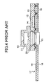
- FIG. 1 is a cross-sectional view showing an example of a semiconductor device having a resin bump.
- FIG. 2 is a cross-sectional view showing another example of the semiconductor device having a resin bump.
- the semiconductor device shown in FIG. 1 has a semiconductor element 1 encapsulated by a mold resin 2.
- a metal film 3 is formed on the bottom (mounting side) of the mold resin 2.
- the metal film 3 is patternized so as to form circuit patterns.
- the semiconductor element 1 is arranged within a mold resin 2 in a face-up state where a circuit formation surface faces upward, and an element-fixing resin 4 is provided on the backside of the semiconductor element 1.
- the element-fixing resin 4 is an adhesive used for fixing the semiconductor element 1 onto the circuit board in the manufacturing process. Electrodes of the semiconductor element 1 are connected to the metal film 3 (pattern wiring) by bonding wires 5.
- the resin bump 6 is formed on the bottom (mounting side) of resin mold 2.
- the resin bump 6 is formed by forming a protruding part made of the mold resin and forming the metal film 3 on the protruding part.
- the metal film 3 positioned at the end of the protruding part serves as an external connection electrode.
- Such a resin bump can be formed by forming on a base board a recess corresponding to the protruding part, forming a resin bump using the recess and thereafter removing the base board.
- FIG. 2 shows the semiconductor device shown in FIG. 1 in which the semiconductor element 1 is arranged in a face-down state where the circuit formation surface faces downward.
- Protruding electrodes are formed on the semiconductor element 1, and the protruding electrodes are connected to the circuit patterns formed by the metal film 3.
- the circuit formation surface of the semiconductor element 1 is filled up with an under-fill material 7.
- the resin bumps 6 are formed on the bottom (mounting side) of the mold resin 2 similar to the semiconductor device shown in FIG. 1.
- the structure of the semiconductor device having resin bumps as shown in FIGS. 1 and 2 is preferably used for producing a small camera module.
- a camera module in which a resin mold provided with a through opening for receiving light and wiring pattern is connected to a circuit board having a through hole, an imaging device being flip-chip mounted on one surface of the resin mold and a lens holder for image formation is mounted on the other surface in a state where the lens holder covers a space above a light-receiving part.
- the imaging device detects a light at the light-receiving part or a device surface on which a micro lens is present and apply a photoelectric transformation to the detected light, and provides the thus-obtained image signal to a signal processing circuit, etc. so as to display a picture on a screen of a display device or the like.
- FIG. 3 is a cross-sectional view of a camera module using the structure of the semiconductor device shown in FIG. 1.
- FIG. 4 is a cross-sectional view of a camera module using the structure of the semiconductor device shown in FIG. 2.
- the camera module shown in FIG. 3 has an image-pickup lens 11 attached to a lens holder 10.
- the lens holder 10 is mounted on the upper surface of a molded body 12 (corresponding to the mold resin 2 of FIG. 1), and an imaging device 13 is attached to the undersurface of the molded body 12.
- a semiconductor element 14 Provided inside the molded body 12 is a semiconductor element 14 (corresponding to the semiconductor element 1 of FIG. 1). Electrodes of the semiconductor element 14 are connected to the pattern wiring which consists of a metal film 15 formed on the bottom (mounting side) of the molded body 12 by the bonding wires.
- Resin bumps 16 are formed on the bottom of the molded body 12, and are electrically connected to the electrodes of the semiconductor element 14 and the imaging device element 13 through the pattern wiring which consists of the metal film 15. Additionally, the resin bumps 16 are connected to the pattern wiring 18 of the wiring board 17.
- the wiring board 17 is a flexible board, and is provided with a pattern wiring made of a copper foil or the like on a polyimide substrate 19.
- the camera module is connected to an external circuit through the wiring board 17.
- a light passed through the lens 10 passes a filter glass 20 and is incident on the imaging surface of the imaging device 13.
- an electric signal corresponding to the image on the imaging surface is output from the imaging device 13.
- the semiconductor element 14 applies image processing to the electric signal from the imaging device 13, and outputs the processed signal to the wiring board 17 through the resin bumps 16.
- the imaging device 13 and the semiconductor element 14 are efficiently connected to the wiring board 17 by the resin bumps 16 formed using the resin of the molded body 12.
- FIG. 4 shows a structure in which the semiconductor element 14 is arranged in a face-down state where the circuit formation surface faces downward in the camera module shown in FIG. 3.
- Projection electrodes are formed on the semiconductor element 14 and are joined to the circuit pattern formed by the metal film 15.
- Japanese Laid-Open Patent Application No. 9-162348 may provide a background of the present invention.
- the semiconductor devices shown in FIGS. 1 and 2 have the structures in which the resin bumps 6 are arranged around the semiconductor element 1. Thus, if the semiconductor element becomes large and a number of electrodes is increased, there is a problem in that the size of the semiconductor device itself becomes large.
- the above-mentioned problem also occurs in the camera modules shown in FIGS. 3 and 4. That is, when the semiconductor element 14 (for example, a processing element) is mounted in addition to the imaging device 13, it is preferable, in order to attempt miniaturization of the module, to take a structure in which the semiconductor element 14 is embedded in the encapsulation resin that forms the molded body 12 unlike the externally attached imaging device. However, it is a subject to miniaturize a module while using the resin bump since the module size becomes inevitably large when forming the resin bumps with the encapsulation resin.
- the semiconductor element 14 for example, a processing element
- a more specific object of the present invention is to provide a miniaturized semiconductor device having resin bumps which is formed by effectively using an area in the bottom (mounting side) of the semiconductor device.
- Another object of the present invention is to miniaturize a camera module having a so-called multi-chip type in which an imaging device and a processor element are mounted.
- a semiconductor device comprising: a semiconductor element; a mold resin encapsulating the semiconductor element; protruding parts protrudingly formed by the mold resin on a mounting surface of the mold resin; and a metal film forming a pattern wiring on the mounting surface of the mold resin, the metal film also formed on the protruding parts so as to constitute external connection terminals together with the protruding parts, wherein electrodes of the semiconductor element are electrically connected to the pattern wiring; and the protruding parts include first protruding parts positioned around the semiconductor element and second protruding parts formed in a mounting area of the semiconductor element on the mounting surface.
- so-called resin bumps are formed on the mounting surface of the semiconductor device.
- the resin bumps constituted by the second protruding parts among the resin bumps are formed in the area where no bumps are formed in a conventional semiconductor device, that is, the area directly under the semiconductor element.
- the resin bumps can be formed all over the entire mounting surface. Therefore, if the semiconductor device according to the present invention has the same size, a number of resin bumps can be increased as compared to the conventional semiconductor device. If, in other words, the resin bumps of the same number as the conventional semiconductor device are formed, the size of the semiconductor device can be reduced, thereby achieving a miniaturized semiconductor device. Additionally, since the resin bumps are also provided in the element mounting area, the degree of freedom in arrangement of the pattern wiring is increased which results in efficient wiring.
- a resin different from the mold resin may be provided between the mounting surface and the semiconductor element so that the second protruding parts are formed by the resin different from the mold resin.
- the electrode of the semiconductor element may be connected to the pattern wiring by a metal wire, and the resin different from the mold resin may serve as a resin for fixing the semiconductor element. Further, the electrodes of the semiconductor element may be protruding electrodes, the semiconductor element being flip-chip mounted to the pattern wiring, and the resin different from the mold resin is an under-fill material.
- the first protruding parts and the second protruding parts may be arranged in a grid pattern on substantially all over the mounting surface.
- a camera module comprising: a lens holder carrying an image-pickup lens; a molded body to which the lens holder is attached; protruding parts formed on a mounting surface of the molded body; a metal film, formed on the protruding parts, forming a pattern wiring on the mounting surface of the molded body so as to constitute external connection terminals together with the protruding parts; a semiconductor element embedded in the molded body; an imaging device mounted on the mounting surface of the molded body and having an imaging surface facing the image-pickup lens through an opening of the molded body; and a wiring board to which the molded body is mounted, wherein the electrodes of the semiconductor element are electrically connected to the pattern wiring, and the protruding parts include first protruding parts located around the semiconductor element and second protruding parts formed on the mounting surface of the semiconductor element within a mounting area.
- a space for providing the wiring pattern can be attained since the resin bumps are also arranged directly under the semiconductor element.
- high-density wiring can be achieved, which results in miniaturization of a camera module.
- a resin different from the mold resin may be provided between the mounting surface and the semiconductor element, and the second protruding parts may be formed of the different resin.
- the electrodes of the semiconductor element may be connected to the pattern wiring by metal wires, and the different resin may serve as a resin for fixing the semiconductor element.
- the electrodes of the semiconductor element may be protruding electrodes, the semiconductor element may be flip-chip connected to the pattern wiring, and the different resin may be an under-fill material.
- the second protruding parts may also be formed in the vicinity of an element mounting area on the mounting surface of the molded body.
- the second protruding parts formed in the vicinity of the element mounting area may be arranged in the vicinity of a center of each side of the element mounting area.
- the first protruding parts may include dummy protruding parts arranged in the vicinity of a periphery of the semiconductor element, and the metal film formed on the dummy protruding parts may be isolated from the wiring pattern.
- the dummy protruding parts may be arranged in the vicinity of each corner of the element mounting area. Further, a part of the imaging device and a part of the semiconductor element may be arranged in an overlapping state with each other.
- a manufacturing method of a semiconductor device comprising the steps of: forming recessed parts in an area including an element mounting area in a mounting surface of a lead frame; forming a metal film on the mounting surface and inside the recessed parts of the lead frame; filling the recessed part formed in the element mounting area with an insulating resin; mounting a semiconductor element in the element mounting area of the lead frame; encapsulating the semiconductor element with a resin on the lead frame; and removing the lead frame.
- a manufacturing method of a camera module comprising the steps of: forming recessed parts in an area including an element mounting area on a mounting surface of a lead frame; forming a metal film on the mounting surface of the lead frame and inside the recessed parts; filling inside the recessed parts formed in the element mounting area with an insulating resin; mounting a semiconductor device in the element mounting area of the lead frame; encapsulating the semiconductor element with a mold resin on the lead frame; filling with the mold resin inside the recessed parts formed in an area other than the element mounting area; removing the lead frame from the molded body; flip-chip mounting an imaging device onto the metal film exposed on the mounting surface of the molded body; mounting the molded body to a wiring board by using the metal film which is formed on protruding parts formed by the insulating resin filled in the recessed parts and the mold resin; and mounting a lens holder provided with an image-pickup lens to the molded body.
- the insulating resin may be for fixing the semiconductor element, and the step of mounting the semiconductor element may include a step of wire-bonding electrodes of the semiconductor element to the metal film. Additionally, the insulating resin may be an under-fill material, and the step of mounting the semiconductor element may include a step of flip-chip bonding electrodes of the semiconductor element to the metal film.
- FIG. 5 is a cross-sectional view of a semiconductor device 30 according to the first embodiment of the present invention.
- parts that are the same as the parts shown in FIG. 1 are given the same reference numerals.
- the semiconductor device 30 has a semiconductor element encapsulated by a mold resin 2 with a metal film 3 formed on a bottom surface (mounting surface) of the mold resin 2.
- the metal film 3 is patternized so as to form a wiring pattern.
- the semiconductor element 1 is arranged in the mold resin 2 in a face-up state where a circuit forming surface faces upward, and an element fixing resin 4 is provided on the backside of the semiconductor element 1.
- the element fixing resin 4 is an adhesive for fixing the semiconductor element 1 to a substrate in a manufacturing process thereof. Electrodes of the semiconductor element 1 are connected to the metal film 3 (pattern wiring) by bonding wires 5.
- Resin bumps 6 are formed in the bottom surface (mounting surface) of the mold resin 2.
- the resin bumps are constituted by forming protruding parts 2a (first protruding parts) by the mold resin 2 and then forming the metal film 3 on the protruding parts 2a so that the metal film 3 located on tops of the protruding parts 2 serve as external connection electrodes.
- Such resin bumps can be formed by forming recessed parts corresponding to the protruding parts on a board, forming the resin bumps by using the recessed parts, and, then removing the substrate. The forming method of the resin bumps will be explained later in the description of a manufacturing method of a camera module.
- the semiconductor device 30 has resin bumps 6A.
- the resin bumps 6A are provided in an area just under the semiconductor element 1. Since the element fixing resin 4 is filled in the area just under the semiconductor element 1, the resin bumps 6A have a structure where the metal film 3 is formed on protruding parts 4a (second protruding parts) formed by the element fixing resin 4. On the other hand, the resin bumps 6 have a structure where the metal film 3 is formed on the protruding parts 2a formed by the mold resin 2 as mentioned above.
- FIG. 6 is a bottom view of the semiconductor device 30 shown in FIG. 5.
- the area indicated by dotted lines is a semiconductor element mounting area, which corresponds to an area jus under the semiconductor element 1.
- the resin bumps 6 and 6A are connected to bonding pads 3b formed by the metal film 3 by a pattern wiring 3a also formed by the metal film 3.
- the resin bumps 6 and the resin bumps 6A are formed on the bottom surface of the semiconductor device 30.
- the resin bumps 6A are formed in the area just under the semiconductor element where no bumps are formed conventionally, the resin bumps 6A are connected to the semiconductor element 1 through the pattern wiring 3a and the bonding pads 3b formed by the metal film 3.
- the resin bumps can be formed over the whole bottom surface of the semiconductor device 30.
- the semiconductor device 30 according to the present embodiment has the same size as a conventional semiconductor device, a number of resin bumps can be increased. In other words, if the same number of resin bumps as a conventional semiconductor device, the size of the semiconductor device 30 can be reduced, which realizes a miniaturized semiconductor device. Additionally, the degree of freedom of arrangement of the pattern wiring is increased by the resin bumps 6A provided in the semiconductor element mounting area, which results in efficient wiring.
- FIG. 7 is a cross-sectional view of a semiconductor device 35 having a structure in which the semiconductor element 1 is arranged in the face-down state where the circuit forming surface faces downward in the semiconductor device 30 shown in FIG. 5.
- Protruding electrodes 1a are formed in the semiconductor element 1, and the protruding electrodes 1a are joined to the wiring pattern formed by the metal film 3. That is, although the semiconductor element 1 shown in FIG. 5 is connected by wire bonding, the semiconductor element 1 shown in FIG. 6 is connected by flip-chip bonding.
- the resin bumps 6 are formed on the bottom surface (mounting surface) of the mold resin 2 similar to the semiconductor device shown in FIG. 2. Although the area just under the semiconductor element 1 is filled up with the under-fill material 7, protruding parts 7a are formed by the under-fill material 7 like the semiconductor device 30 shown in FIG. 5. Additionally, the metal film 3 is formed on the protruding parts 7a so as to constitute the resin bumps 6B.
- the resin bumps 6A are formed by the protruding parts 4a formed of the element fixing resin 4 in the semiconductor device 30
- the resin bumps 6B are formed by the protruding parts 7a formed of the under-fill material 7 in the semiconductor device 35. Since each of the element fixing resins 4 and the under-fill material is formed of an insulating resin etc., the resin bumps 6A and 6B have a function the same as that of external connection terminals.
- the semiconductor device 35 shown in FIG. 7 contributes to the miniaturization of a semiconductor device similar to the semiconductor device 30.
- FIG. 8 is a cross-sectional view of the camera module 40 according to the second embodiment of the present invention.
- parts that are the same as the parts shown in FIG. 3 are given the same reference numerals.
- a lens holder 10 equipped with an image-pickup lens 11 is attached to an upper surface of the molded body 12, and an imaging device 13 is attached to a lower surface of the molded body 12.
- a semiconductor element 14 is arranged inside the molded body as a processor element. Electrodes of the semiconductor element 14 are connected by bonding wires 14 to the pattern wiring which is made by a metal film 15 formed on the bottom surface (mounting surface) of the molded body 12.
- the resin bumps 16 as shown in the above-mentioned FIG. 5 are formed on the bottom surface of the molded body 12, and the resin bumps 16 are electrically connected to the semiconductor element 14 and the imaging device 13 through the pattern wiring which is formed by the metal film 15. Additionally, resin bumps 16A are formed in an area just under the semiconductor element 14 by utilizing protruding parts 42a formed of an element fixing resin 42. The resin bumps 16 and 16A are connected to the pattern wiring 18 of a wiring board 17.
- the wiring board 17 is a flexible board, and is provided with a pattern wiring made of a copper foil etc. applied onto a board 19 made of a polyimide tape or the like.
- An opening 17a is formed in the wiring board and the imaging device has protruding electrodes 13a so that the imaging device 13 is mounted onto the bottom surface (mounting surface) of the molded body in a state where the imaging device 13 is situated within the opening 17a.
- An under-fill material 43 is filled between the imaging device 13 and the molded body 12.
- the camera module 40 is connected through the wiring board 17 to an external circuit of a portable equipment such as a portable telephone or a small computer.
- a light which passed through the lens 10 passes a filter glass 20 and is incident on the imaging surface of the imaging device 13, and thereby, an electric signal corresponding to an image is output from the imaging device 13.
- the semiconductor element 14 applied an image processing to the electric signal from the imaging device 13, and outputs the processed signal to the wiring board 17 through the resin bumps 16.
- the imaging device 13 and the semiconductor element 14 are efficiently connected to the wiring board 17 by the resin bumps 16 formed by the resin of the molded body 12 and the resin bumps 16A formed by the element fixing resin 42.
- FIG. 9 is an illustration for explaining the manufacturing process of the camera module 40.
- a lead frame 45 made of a copper plate or the like is prepared, and recessed parts 45a are formed on a surface of the lead frame 45 as shown in FIG. 9-(a).
- the recessed parts 45a are formed in a configuration and at positions corresponding to the resin bumps 16 and 16A formed on the bottom surface of the molded body 12.
- the metal film 15 is formed on the surface of the lead frame 45.
- the metal film 15 is patternized so as to be the pattern wiring and the bonding pads formed in an inner surface of the recessed parts 45a and the surface of the lead frame.
- the element fixing resin 42 made of an insulating resin is applied in the element mounting area of the lead frame 45. During the application, the element fixing resin 42 is filled in the recessed parts 45a.
- the semiconductor element 14 is laid on the element fixing resin 42, and the element fixing resin 42 is cured. After the element fixing resin 42 is cured, the electrodes of the semiconductor element 14 are connected by the bonding wires 41 to the bonding pads formed by the metal film 15.
- the molded body 12 is formed by a mold resin in the board 45.
- the mold resin is filled in the recessed parts other than that formed in the element mounting area.
- the lead frame 45 is removed from the molded body 12.
- the removal of the lead frame 45 is performed using an exfoliating method, a dissolving method using etching, etc.
- the imaging device 13 is flip-chip bonded to the bonding pads formed by the metal film 15 exposed on the bottom surface (mounting surface) of the molded body 12. Then, the resin bumps 16 and 16A are connected to the pattern wiring 18 of the wiring board 17 in a state where the imaging device 13 is situated in the opening 17a of the wiring board 17. Subsequently, the lens holder 10 equipped with the lens 11 and filter glass 20 is attached to the molded body 12, which results in a completion of the camera module 40.
- a space sufficient for providing the wiring pattern can be reserved since the resin bumps 16A are arranged also directly under the semiconductor element 14. Thereby, high-density wiring can be achieved, and, as a result, miniaturization of a camera module can be attained. Additionally, the element mounting on the resin bumps can be performed since the protruding parts 42a for the resin bumps are formed using the element fixing resin used as an adhesive of a semiconductor element.
- an insulating resin As the element fixing resin; it is necessary to use an insulating resin as the element fixing resin since it is necessary to prevent short circuiting of metal wires during die-bonding.
- an insulating resin is it preferable to use a resin having a high-resistance to an etchant used for dissolving and removing a board and having high-adhesion with the metal film 15.
- FIG. 10 is a cross-sectional view of a camera module which is constituted by flip-chip bonding the semiconductor element 14 of the camera module 40 shown in FIG. 8.
- parts that are the same as the parts shown in FIG. 8 are given the same reference numerals, and descriptions thereof will be omitted.
- the camera module 50 shown in FIG. 10 is constituted by flip-chip mounting the semiconductor element 14 to the metal film 15 exposed on the bottom surface (mounting surface) of the molded body 12.
- An under-fill material 51 is provided under the semiconductor element 14 so that protruding parts 51a are formed by the under-fill material 51.
- the metal film 15 is formed on the outer surface of the protruding parts 51a so as to form the resin bumps 16B.
- FIG. 11 is an illustration for explaining a manufacturing method of the camera module 50 shown in FIG. 10.
- the manufacturing method of the camera module 50 is basically the same as the manufacturing method of the camera module 40 sown in FIG. 9 except for the semiconductor element 14 being flip-chip mounted.
- the under-fill material 51 made of an anisotropically conductive resin is applied in the element mounting area, as shown in FIG. 11-(a).
- the under-fill material 15 is filled in the recessed parts 45a, which correspond to the resin bumps 16B.
- the semiconductor element 14 is flip-chip mounted from above the under-fill material 51.
- the molded body 12 is formed on the lead frame 45.
- the subsequent process is the same as the process shown in FIG. 9, and explanation thereof will be omitted.
- the above-mentioned camera module 50 has the same advantage as the camera module 40. Additionally, the semiconductor element 14 can be easily mounted onto the resin bumps by forming the protruding parts by the under-fill material directly under the semiconductor element 14 so as to form the resin bumps and further performing flip chip bonding to the flat metal film 15 (bonding pads) on the lead frame 45. Since the approach of connecting the semiconductor element 14 according to the flip-chip bonding method can make the mounting area smaller than using the wire-bonding method, there is an advantage that the further miniaturization of a camera module can be attained.
- the manufacturing method of the camera module 50 it is possible in construction to form only the resin bumps by a resin different from an encapsulation resin and the flip-chip bonding is performed in the manufacturing process so that the positions of the recessed parts (parts of a mold die corresponding to the resin bumps) of the lead frame coincide with the positions of the bumps.
- the above-mentioned method there is disadvantages in the above-mentioned method in that: 1) it is difficult to fill the resin bumps sorely when the size of the resin bumps is small; 2) there is limits in processing size and pitch of the recessed parts formed by etching the lead frame; and 3) bonding cannot be performed unless the metal bumps, which are used when flip-chip bonding, have a size larger than the depth of the recessed parts.
- the element mounting onto the resin bumps can be easily achieved by filling an insulating resin directly under the semiconductor element 14 including the resin bumps so as to use the insulating resin as an adhesive (an under-fill material in the case of the camera module 50), and further performing the flip-chip bonding to the flat metal film on the lead frame.
- FIG. 12 is a cross-sectional view showing the variation of the camera module 50.
- parts that are the same as the parts shown in FIG. 10 are give the same reference numerals, and descriptions thereof will be omitted.
- the camera module 60 shown in FIG. 12 has a structure basically the same as the camera module shown in FIG. 10 except for the resin bumps being provided no only directly under the element mounting area but also in the vicinity of the resin bumps. That is, as shown in FIG. 12, resin bumps 16C are formed in the vicinity of the area (element mounting area) directly under the semiconductor element 14 or in a state where the resin bumps are bridged over the element mounting area and an area outside the element mounting area. Similar to the resin bumps 16B, the resin bumps 16C are formed using protruding parts 51a formed of the under-fill material 5.
- FIG. 13 is an illustration for explaining a manufacturing process of the camera module 60.
- the manufacturing process of the camera module 60 is basically the same as the manufacturing process of the camera module 50 shown in FIG. 11 except for the recessed parts 45b being formed in the vicinity of the element mounting area of the lead frame 45.
- the under-fill material 51 applied to the element mounting area of the lead frame 45 flows into recessed parts 45b formed in the vicinity of the element mounting area. In this state, the under-fill material 51 flows into a part of the recessed parts 45b.
- the excessive under-fill material 51 between the semiconductor element 14 and the lead frame 45 overflows from the element mounting area and flows into the recessed parts 45b, and, thereby, the recessed parts 45b are completely filled with the under-fill material 51. That is, the recessed parts 45b functions as a dam where the overflowing under-fill material 51 flows in. Since an amount of overflowing under-fill material 51 is maximum at the center of each side of the element mounting area, it is preferable to provide the recessed parts 45b close to the center of each side of the element mounting area.
- the resin bumps 16C do not only function as external connection terminals but also has an effect to control the overflowing amount of the under-fill material 51 during manufacture. It should be noted that the process shown in FIG. 13 (c)-(e) is the same as that of FIG. 11 (c)-(e), and descriptions thereof will be omitted.
- the recessed parts 45a exist also directly under the semiconductor element 14, and the process is performed on the assumption that the recessed parts are filled with the under-fill material. For this reason, there is an advantage that the control of the amount of application is easier than a conventional method, which makes the manufacturing process easier.
- the resin bumps located around the semiconductor element 14 are separated away from the location to some extent so as to prevent the under-fill material 51 from being filled in the recessed parts.
- it becomes unnecessary to separate the resin bumps from the element mounting area by forming the above-mentioned resin bumps 16C there is a flexibility in the wiring pattern design, which provides an advantage that high-density wiring can be achieved.
- FIG. 14 is a cross-sectional view of a camera module 70 which is provided with resin bumps for support.
- parts that are the same as the parts shown in FIG. 8 are given the same reference numerals, and descriptions thereof will be omitted.
- the camera module 70 has a structure basically the same as the camera module 40 shown in FIG. 8 except of resin bumps 16D for support (also referred to as dummy resin bumps) being provided. (it is also called a dummy resin bump).
- the resin bumps 16D for support are isolated resin bumps which are not connected to the patterned wire and are arranged near the semiconductor element 14. Similar to the resin bumps 16, the resin bumps 16D for support are formed using protruding parts 12a (dummy protruding parts) formed of a molding encapsulation resin for forming the molded body 12.
- the structure in which the resin bumps 16D for support are provided is effective when the adhesion of the metal film 15 to the element fixing resin which constitute the resin bumps 16A directly under the semiconductor element is inferior to the adhesion of the metal film 15 to the molding encapsulation resin. That is, if the adhesion of the metal film 15 to the resin protruding parts 51a for the resin bumps is poor, a connection strength of the resin bumps 16A to the lands of the wiring board 17 is small and, thus, exfoliation tends to occur between the resin and metal when a mechanical stress is continuously applied, which may deteriorate reliability.
- resin bumps 16D for support are arranged around the semiconductor element 14, and are connected to the board.
- the resin bumps 16A By surrounding the resin bumps 16A having a small connection strength with the resin bumps 16 having a large connection strength, the resin bumps 16A can be supported at the circumference of the semiconductor element 14 so that resin bumps 16A may maintain a good connection state. For example, it is preferable to arrange the resin bumps 16D for support near the four corners of the semiconductor element 14.
- FIG. 15 is a cross-sectional view showing an example in which the above-mentioned resin bumps 16D for support are provided to the camera module shown in FIG. 10.
- the camera module 75 shown in FIG. 15 has a structure basically the same as the camera module 50 shown in FIG. 10 except for the resin bumps 16D for support being provided.
- the resin bumps 16B are formed using protruding parts 51a formed of the under-fill material 51 like the camera module 50, the adhesion between the under-fill material 51 and the metal film 15 which constitute resin bumps 16B may be inferior to the adhesion between the molding encapsulation resin and the metal film 15. In such a case, the structure provided with the resin bumps 16D for support is effective.
- FIG. 16 is a cross-sectional view of a camera module 80 in which a part of an imaging device and a part of a semiconductor element are overlapped with each other.
- parts that are the same as the parts shown in FIG. 8 are given the same reference numerals, and descriptions thereof will be omitted.
- the camera module 80 has a structure basically the same as the camera module 40 shown in FIG. 8 except that a part of an imaging device and a part of a semiconductor element are arranged in an overlapping state with each other. If the size of the imaging device 13 is large and the flip-chip connected portion is away from the opening 12b of the molded body 12 to some extent, the molded body 12 can be miniaturized by arranging a part of the imaging device 13 and a part of the semiconductor element 14 in an overlapping state with each other. Consequently, the miniaturization of the camera module can be attained.
- a space occupied by the molded body 12 can be efficiently used by incorporating a passive element 81 such as a capacitor into the molded part above the imaging device 13.
- FIG. 17 is a cross-sectional view showing an example in which an arrangement where a part of an imaging device and a part of a semiconductor element are overlapped with each other is applied to the camera module 50 shown in FIG. 10.
- a camera module 85 shown in FIG. 17 has a structure basically the same as the camera module 40 shown in FIG. 8 except that a part of an imaging device and a part of a semiconductor element are overlapped with each other.
- the camera module 85 has the same advantages as the camera module 80 shown in FIG. 16.
Abstract
Description
- The present invention relates to semiconductor devices and, more particularly, to a semiconductor device suitable for a camera module which integrally packages a light-receiving element and an image-pickup lens.
- In recent years, portable telephones and portable personal computers equipped with a small camera have been developed. For example, a portable telephone equipped with a small camera picks up an image of a calling person by the small camera so as to acquire image data and sends the image data to a person on the line. Generally, such a small camera is constituted by a CMOS sensor and a lens.
- Miniaturization of portable telephones and portable personal computers has been progressed further, and there is also a demand for miniaturization of small cameras used for these equipments. In order to satisfy the demand for miniaturization of such a small camera, a camera module which integrates a lens and a CMOS sensor has been developed.
- The above-mentioned camera module is formed as a small module by incorporating an image-pickup lens, an imaging device and a semiconductor element into a mold resin. The camera module has the same structure as a semiconductor device which has a semiconductor element encapsulated in a mold resin, and is connectable to a circuit board by using bump-chip-carrier (BCC) electrodes as external connection terminals. As an example of a BCC electrode, there is an electrode formed of a protrusion made of a mold resin and covered with a metal film on an outer surface of the protrusion. Such a BCC electrode is generally referred to as a resin bump.
- FIG. 1 is a cross-sectional view showing an example of a semiconductor device having a resin bump. FIG. 2 is a cross-sectional view showing another example of the semiconductor device having a resin bump.
- The semiconductor device shown in FIG. 1 has a
semiconductor element 1 encapsulated by amold resin 2. Ametal film 3 is formed on the bottom (mounting side) of themold resin 2.
Themetal film 3 is patternized so as to form circuit patterns. Thesemiconductor element 1 is arranged within amold resin 2 in a face-up state where a circuit formation surface faces upward, and an element-fixing resin 4 is provided on the backside of thesemiconductor element 1. The element-fixing resin 4 is an adhesive used for fixing thesemiconductor element 1 onto the circuit board in the manufacturing process. Electrodes of thesemiconductor element 1 are connected to the metal film 3 (pattern wiring) bybonding wires 5. - The
resin bump 6 is formed on the bottom (mounting side) ofresin mold 2. Theresin bump 6 is formed by forming a protruding part made of the mold resin and forming themetal film 3 on the protruding part. Themetal film 3 positioned at the end of the protruding part serves as an external connection electrode. Such a resin bump can be formed by forming on a base board a recess corresponding to the protruding part, forming a resin bump using the recess and thereafter removing the base board. - FIG. 2 shows the semiconductor device shown in FIG. 1 in which the
semiconductor element 1 is arranged in a face-down state where the circuit formation surface faces downward. Protruding electrodes are formed on thesemiconductor element 1, and the protruding electrodes are connected to the circuit patterns formed by themetal film 3.
The circuit formation surface of thesemiconductor element 1 is filled up with an under-fill material 7. Theresin bumps 6 are formed on the bottom (mounting side) of themold resin 2 similar to the semiconductor device shown in FIG. 1. - The structure of the semiconductor device having resin bumps as shown in FIGS. 1 and 2 is preferably used for producing a small camera module.
- As a structure of the camera module which can be miniaturized, there is suggested a camera module in which a resin mold provided with a through opening for receiving light and wiring pattern is connected to a circuit board having a through hole, an imaging device being flip-chip mounted on one surface of the resin mold and a lens holder for image formation is mounted on the other surface in a state where the lens holder covers a space above a light-receiving part. The imaging device detects a light at the light-receiving part or a device surface on which a micro lens is present and apply a photoelectric transformation to the detected light, and provides the thus-obtained image signal to a signal processing circuit, etc. so as to display a picture on a screen of a display device or the like.
- FIG. 3 is a cross-sectional view of a camera module using the structure of the semiconductor device shown in FIG. 1. FIG. 4 is a cross-sectional view of a camera module using the structure of the semiconductor device shown in FIG. 2.
- The camera module shown in FIG. 3 has an image-
pickup lens 11 attached to alens holder 10. Thelens holder 10 is mounted on the upper surface of a molded body 12 (corresponding to themold resin 2 of FIG. 1), and animaging device 13 is attached to the undersurface of themolded body 12. Provided inside the moldedbody 12 is a semiconductor element 14 (corresponding to thesemiconductor element 1 of FIG. 1). Electrodes of thesemiconductor element 14 are connected to the pattern wiring which consists of ametal film 15 formed on the bottom (mounting side) of the moldedbody 12 by the bonding wires. -
Resin bumps 16 are formed on the bottom of the moldedbody 12, and are electrically connected to the electrodes of thesemiconductor element 14 and theimaging device element 13 through the pattern wiring which consists of themetal film 15. Additionally, theresin bumps 16 are connected to thepattern wiring 18 of thewiring board 17. Thewiring board 17 is a flexible board, and is provided with a pattern wiring made of a copper foil or the like on apolyimide substrate 19. The camera module is connected to an external circuit through thewiring board 17. - In the camera module of the above-mentioned structure, a light passed through the
lens 10 passes afilter glass 20 and is incident on the imaging surface of theimaging device 13. Thereby, an electric signal corresponding to the image on the imaging surface is output from theimaging device 13. Thesemiconductor element 14 applies image processing to the electric signal from theimaging device 13, and outputs the processed signal to thewiring board 17 through theresin bumps 16. Thus, theimaging device 13 and thesemiconductor element 14 are efficiently connected to thewiring board 17 by theresin bumps 16 formed using the resin of the moldedbody 12. - FIG. 4 shows a structure in which the
semiconductor element 14 is arranged in a face-down state where the circuit formation surface faces downward in the camera module shown in FIG. 3. Projection electrodes are formed on thesemiconductor element 14 and are joined to the circuit pattern formed by themetal film 15. - It should be noted that Japanese Laid-Open Patent Application No. 9-162348 may provide a background of the present invention.
- The semiconductor devices shown in FIGS. 1 and 2 have the structures in which the
resin bumps 6 are arranged around thesemiconductor element 1. Thus, if the semiconductor element becomes large and a number of electrodes is increased, there is a problem in that the size of the semiconductor device itself becomes large. - The above-mentioned problem also occurs in the camera modules shown in FIGS. 3 and 4. That is, when the semiconductor element 14 (for example, a processing element) is mounted in addition to the
imaging device 13, it is preferable, in order to attempt miniaturization of the module, to take a structure in which thesemiconductor element 14 is embedded in the encapsulation resin that forms themolded body 12 unlike the externally attached imaging device. However, it is a subject to miniaturize a module while using the resin bump since the module size becomes inevitably large when forming the resin bumps with the encapsulation resin. - It is a general object of the present invention to provide an improved and useful semiconductor device in which the above-mentioned problems are eliminated.
- A more specific object of the present invention is to provide a miniaturized semiconductor device having resin bumps which is formed by effectively using an area in the bottom (mounting side) of the semiconductor device.
- Another object of the present invention is to miniaturize a camera module having a so-called multi-chip type in which an imaging device and a processor element are mounted.
- In order to achieve the above-mentioned objects, there is provided according to one aspect of the present invention a semiconductor device comprising: a semiconductor element; a mold resin encapsulating the semiconductor element; protruding parts protrudingly formed by the mold resin on a mounting surface of the mold resin; and a metal film forming a pattern wiring on the mounting surface of the mold resin, the metal film also formed on the protruding parts so as to constitute external connection terminals together with the protruding parts, wherein electrodes of the semiconductor element are electrically connected to the pattern wiring; and the protruding parts include first protruding parts positioned around the semiconductor element and second protruding parts formed in a mounting area of the semiconductor element on the mounting surface.
- According to above-mentioned invention, so-called resin bumps are formed on the mounting surface of the semiconductor device. The resin bumps constituted by the second protruding parts among the resin bumps are formed in the area where no bumps are formed in a conventional semiconductor device, that is, the area directly under the semiconductor element. Thereby, in the semiconductor device according to the present invention, the resin bumps can be formed all over the entire mounting surface. Therefore, if the semiconductor device according to the present invention has the same size, a number of resin bumps can be increased as compared to the conventional semiconductor device. If, in other words, the resin bumps of the same number as the conventional semiconductor device are formed, the size of the semiconductor device can be reduced, thereby achieving a miniaturized semiconductor device. Additionally, since the resin bumps are also provided in the element mounting area, the degree of freedom in arrangement of the pattern wiring is increased which results in efficient wiring.
- In the above-mentioned semiconductor device, a resin different from the mold resin may be provided between the mounting surface and the semiconductor element so that the second protruding parts are formed by the resin different from the mold resin. The electrode of the semiconductor element may be connected to the pattern wiring by a metal wire, and the resin different from the mold resin may serve as a resin for fixing the semiconductor element. Further, the electrodes of the semiconductor element may be protruding electrodes, the semiconductor element being flip-chip mounted to the pattern wiring, and the resin different from the mold resin is an under-fill material.
- In the semiconductor device according to the present invention, the first protruding parts and the second protruding parts may be arranged in a grid pattern on substantially all over the mounting surface.
- Additionally, there is provided according to another aspect of the present invention a camera module comprising: a lens holder carrying an image-pickup lens; a molded body to which the lens holder is attached; protruding parts formed on a mounting surface of the molded body; a metal film, formed on the protruding parts, forming a pattern wiring on the mounting surface of the molded body so as to constitute external connection terminals together with the protruding parts; a semiconductor element embedded in the molded body; an imaging device mounted on the mounting surface of the molded body and having an imaging surface facing the image-pickup lens through an opening of the molded body; and a wiring board to which the molded body is mounted, wherein the electrodes of the semiconductor element are electrically connected to the pattern wiring, and the protruding parts include first protruding parts located around the semiconductor element and second protruding parts formed on the mounting surface of the semiconductor element within a mounting area.
- According to the above-mentioned invention, a space for providing the wiring pattern can be attained since the resin bumps are also arranged directly under the semiconductor element. Thus, high-density wiring can be achieved, which results in miniaturization of a camera module.
- In the camera module according to the present invention, a resin different from the mold resin may be provided between the mounting surface and the semiconductor element, and the second protruding parts may be formed of the different resin. The electrodes of the semiconductor element may be connected to the pattern wiring by metal wires, and the different resin may serve as a resin for fixing the semiconductor element. The electrodes of the semiconductor element may be protruding electrodes, the semiconductor element may be flip-chip connected to the pattern wiring, and the different resin may be an under-fill material. The second protruding parts may also be formed in the vicinity of an element mounting area on the mounting surface of the molded body. The second protruding parts formed in the vicinity of the element mounting area may be arranged in the vicinity of a center of each side of the element mounting area.
- Additionally, the first protruding parts may include dummy protruding parts arranged in the vicinity of a periphery of the semiconductor element, and the metal film formed on the dummy protruding parts may be isolated from the wiring pattern. The dummy protruding parts may be arranged in the vicinity of each corner of the element mounting area. Further, a part of the imaging device and a part of the semiconductor element may be arranged in an overlapping state with each other.
- Additionally, there is provided according to another aspect of the present invention a manufacturing method of a semiconductor device comprising the steps of: forming recessed parts in an area including an element mounting area in a mounting surface of a lead frame; forming a metal film on the mounting surface and inside the recessed parts of the lead frame; filling the recessed part formed in the element mounting area with an insulating resin; mounting a semiconductor element in the element mounting area of the lead frame; encapsulating the semiconductor element with a resin on the lead frame; and removing the lead frame.
- Further, there is provided according to another aspect of the present invention a manufacturing method of a camera module, comprising the steps of: forming recessed parts in an area including an element mounting area on a mounting surface of a lead frame; forming a metal film on the mounting surface of the lead frame and inside the recessed parts; filling inside the recessed parts formed in the element mounting area with an insulating resin; mounting a semiconductor device in the element mounting area of the lead frame; encapsulating the semiconductor element with a mold resin on the lead frame; filling with the mold resin inside the recessed parts formed in an area other than the element mounting area; removing the lead frame from the molded body; flip-chip mounting an imaging device onto the metal film exposed on the mounting surface of the molded body; mounting the molded body to a wiring board by using the metal film which is formed on protruding parts formed by the insulating resin filled in the recessed parts and the mold resin; and mounting a lens holder provided with an image-pickup lens to the molded body.
- In the above-mentioned manufacturing method of a camera module, the insulating resin may be for fixing the semiconductor element, and the step of mounting the semiconductor element may include a step of wire-bonding electrodes of the semiconductor element to the metal film. Additionally, the insulating resin may be an under-fill material, and the step of mounting the semiconductor element may include a step of flip-chip bonding electrodes of the semiconductor element to the metal film.
- Other objects, features and advantages of the present invention will become more apparent from the following detailed description when read in conjunction with the accompanying drawings.
-
- FIG. 1 is a cross-sectional view showing an example of a semiconductor device having resin bumps;
- FIG. 2 is a cross-sectional view showing another example of a semiconductor device having resin bumps;
- FIG. 3 is a cross-sectional view showing an example of a camera module having resin bumps;
- FIG. 4 is a cross-sectional view showing another example of a camera module having resin bumps;
- FIG. 5 is a cross-sectional view showing a semiconductor device according to a first embodiment of the present invention;
- FIG. 6 is a bottom view of the semiconductor device shown in FIG. 5;
- FIG. 7 is a cross-sectional view showing another example of the semiconductor device according to the first embodiment of the present invention;
- FIG. 8 is a cross-sectional view showing a camera module according of a second embodiment of the present invention;
- FIG. 9 is an illustration for explaining a manufacturing process of the camera module shown in FIG. 8.
- FIG. 10 is a cross-sectional view showing another example of the camera module according of the second embodiment of the present invention;
- FIG. 11 is an illustration for explaining a manufacturing process of the camera module shown in FIG. 10;
- FIG. 12 is a cross-sectional view showing a variation of the camera module shown in FIG. 10;
- FIG. 13 is an illustration for explaining a manufacturing process of the camera module shown in FIG. 12;
- FIG. 14 is a cross-sectional view showing another variation of the camera module shown in FIG. 8;
- FIG. 15 is a cross-sectional view showing another variation of the camera module shown in FIG. 10;
- FIG. 16 is a cross-sectional view showing yet another variation of the camera module shown in FIG. 8; and
- FIG. 17 is a cross-sectional view showing yet another variation of the camera module shown in FIG. 10.
-
- A description will now be given, with reference to FIG. 5, of a first embodiment of the present invention. FIG. 5 is a cross-sectional view of a
semiconductor device 30 according to the first embodiment of the present invention. In FIG. 5, parts that are the same as the parts shown in FIG. 1 are given the same reference numerals. - The
semiconductor device 30 according to the first embodiment of the present invention has a semiconductor element encapsulated by amold resin 2 with ametal film 3 formed on a bottom surface (mounting surface) of themold resin 2. Themetal film 3 is patternized so as to form a wiring pattern. Thesemiconductor element 1 is arranged in themold resin 2 in a face-up state where a circuit forming surface faces upward, and anelement fixing resin 4 is provided on the backside of thesemiconductor element 1. Theelement fixing resin 4 is an adhesive for fixing thesemiconductor element 1 to a substrate in a manufacturing process thereof. Electrodes of thesemiconductor element 1 are connected to the metal film 3 (pattern wiring) bybonding wires 5. - Resin bumps 6 are formed in the bottom surface (mounting surface) of the
mold resin 2. The resin bumps are constituted by formingprotruding parts 2a (first protruding parts) by themold resin 2 and then forming themetal film 3 on the protrudingparts 2a so that themetal film 3 located on tops of the protrudingparts 2 serve as external connection electrodes. Such resin bumps can be formed by forming recessed parts corresponding to the protruding parts on a board, forming the resin bumps by using the recessed parts, and, then removing the substrate. The forming method of the resin bumps will be explained later in the description of a manufacturing method of a camera module. - In addition to the resin bumps 6, the
semiconductor device 30 has resin bumps 6A. The resin bumps 6A are provided in an area just under thesemiconductor element 1. Since theelement fixing resin 4 is filled in the area just under thesemiconductor element 1, the resin bumps 6A have a structure where themetal film 3 is formed on protrudingparts 4a (second protruding parts) formed by theelement fixing resin 4. On the other hand, the resin bumps 6 have a structure where themetal film 3 is formed on the protrudingparts 2a formed by themold resin 2 as mentioned above. - FIG. 6 is a bottom view of the
semiconductor device 30 shown in FIG. 5. In FIG. 6, the area indicated by dotted lines is a semiconductor element mounting area, which corresponds to an area jus under thesemiconductor element 1. The resin bumps 6 and 6A are connected tobonding pads 3b formed by themetal film 3 by apattern wiring 3a also formed by themetal film 3. - As mentioned above, in the present embodiment, the resin bumps 6 and the resin bumps 6A are formed on the bottom surface of the
semiconductor device 30. Although the resin bumps 6A are formed in the area just under the semiconductor element where no bumps are formed conventionally, the resin bumps 6A are connected to thesemiconductor element 1 through thepattern wiring 3a and thebonding pads 3b formed by themetal film 3. Thus, the resin bumps can be formed over the whole bottom surface of thesemiconductor device 30. - Therefore, if the
semiconductor device 30 according to the present embodiment has the same size as a conventional semiconductor device, a number of resin bumps can be increased. In other words, if the same number of resin bumps as a conventional semiconductor device, the size of thesemiconductor device 30 can be reduced, which realizes a miniaturized semiconductor device. Additionally, the degree of freedom of arrangement of the pattern wiring is increased by the resin bumps 6A provided in the semiconductor element mounting area, which results in efficient wiring. - FIG. 7 is a cross-sectional view of a
semiconductor device 35 having a structure in which thesemiconductor element 1 is arranged in the face-down state where the circuit forming surface faces downward in thesemiconductor device 30 shown in FIG. 5. Protrudingelectrodes 1a are formed in thesemiconductor element 1, and the protrudingelectrodes 1a are joined to the wiring pattern formed by themetal film 3. That is, although thesemiconductor element 1 shown in FIG. 5 is connected by wire bonding, thesemiconductor element 1 shown in FIG. 6 is connected by flip-chip bonding. - In the
semiconductor device 35, the resin bumps 6 are formed on the bottom surface (mounting surface) of themold resin 2 similar to the semiconductor device shown in FIG. 2. Although the area just under thesemiconductor element 1 is filled up with the under-fill material 7, protrudingparts 7a are formed by the under-fill material 7 like thesemiconductor device 30 shown in FIG. 5. Additionally, themetal film 3 is formed on the protrudingparts 7a so as to constitute the resin bumps 6B. - Although the resin bumps 6A are formed by the protruding
parts 4a formed of theelement fixing resin 4 in thesemiconductor device 30, the resin bumps 6B are formed by the protrudingparts 7a formed of the under-fill material 7 in thesemiconductor device 35. Since each of theelement fixing resins 4 and the under-fill material is formed of an insulating resin etc., the resin bumps 6A and 6B have a function the same as that of external connection terminals. - As mentioned above, since the resin bumps 6B of the
semiconductor device 35 shown in FIG. 7 are formed in the area just under thesemiconductor element 1 similar to thesemiconductor device 30 shown in FIG. 5, thesemiconductor device 35 shown in FIG. 7 contributes to the miniaturization of a semiconductor device similar to thesemiconductor device 30. - Next, a description will be given, with reference to FIG. 8, of a camera module which is a semiconductor device according to a second embodiment of the present invention. FIG. 8 is a cross-sectional view of the
camera module 40 according to the second embodiment of the present invention. In FIG. 8, parts that are the same as the parts shown in FIG. 3 are given the same reference numerals. - In the
camera module 40 shown in FIG. 8, alens holder 10 equipped with an image-pickup lens 11 is attached to an upper surface of the moldedbody 12, and animaging device 13 is attached to a lower surface of the moldedbody 12. Asemiconductor element 14 is arranged inside the molded body as a processor element. Electrodes of thesemiconductor element 14 are connected by bondingwires 14 to the pattern wiring which is made by ametal film 15 formed on the bottom surface (mounting surface) of the moldedbody 12. - The resin bumps 16 as shown in the above-mentioned FIG. 5 are formed on the bottom surface of the molded
body 12, and the resin bumps 16 are electrically connected to thesemiconductor element 14 and theimaging device 13 through the pattern wiring which is formed by themetal film 15. Additionally, resin bumps 16A are formed in an area just under thesemiconductor element 14 by utilizingprotruding parts 42a formed of anelement fixing resin 42. The resin bumps 16 and 16A are connected to thepattern wiring 18 of awiring board 17. - The
wiring board 17 is a flexible board, and is provided with a pattern wiring made of a copper foil etc. applied onto aboard 19 made of a polyimide tape or the like. Anopening 17a is formed in the wiring board and the imaging device has protrudingelectrodes 13a so that theimaging device 13 is mounted onto the bottom surface (mounting surface) of the molded body in a state where theimaging device 13 is situated within theopening 17a. An under-fill material 43 is filled between theimaging device 13 and the moldedbody 12. Thecamera module 40 is connected through thewiring board 17 to an external circuit of a portable equipment such as a portable telephone or a small computer. - In the
camera module 40 of the above-mentioned structure, a light which passed through thelens 10 passes afilter glass 20 and is incident on the imaging surface of theimaging device 13, and thereby, an electric signal corresponding to an image is output from theimaging device 13. Thesemiconductor element 14 applied an image processing to the electric signal from theimaging device 13, and outputs the processed signal to thewiring board 17 through the resin bumps 16. Thus, theimaging device 13 and thesemiconductor element 14 are efficiently connected to thewiring board 17 by the resin bumps 16 formed by the resin of the moldedbody 12 and the resin bumps 16A formed by theelement fixing resin 42. - Next, a description will be given, with reference to FIG. 9, of a manufacturing method of the cameral module shown in FIG. 8. FIG. 9 is an illustration for explaining the manufacturing process of the
camera module 40. - First, a
lead frame 45 made of a copper plate or the like is prepared, and recessedparts 45a are formed on a surface of thelead frame 45 as shown in FIG. 9-(a). The recessedparts 45a are formed in a configuration and at positions corresponding to the resin bumps 16 and 16A formed on the bottom surface of the moldedbody 12. Themetal film 15 is formed on the surface of thelead frame 45. Themetal film 15 is patternized so as to be the pattern wiring and the bonding pads formed in an inner surface of the recessedparts 45a and the surface of the lead frame. Then, theelement fixing resin 42 made of an insulating resin is applied in the element mounting area of thelead frame 45. During the application, theelement fixing resin 42 is filled in the recessedparts 45a. - Next, as shown in FIG. 9-(b), the
semiconductor element 14 is laid on theelement fixing resin 42, and theelement fixing resin 42 is cured. After theelement fixing resin 42 is cured, the electrodes of thesemiconductor element 14 are connected by thebonding wires 41 to the bonding pads formed by themetal film 15. - Then, as shown in FIG. 9-(c), the molded
body 12 is formed by a mold resin in theboard 45. At this time, the mold resin is filled in the recessed parts other than that formed in the element mounting area. - After the molded
body 12 is formed, as shown in FIG. 9-(d), thelead frame 45 is removed from the moldedbody 12. The removal of thelead frame 45 is performed using an exfoliating method, a dissolving method using etching, etc. - Thereafter, as shown in FIG. 9-(e), the
imaging device 13 is flip-chip bonded to the bonding pads formed by themetal film 15 exposed on the bottom surface (mounting surface) of the moldedbody 12. Then, the resin bumps 16 and 16A are connected to thepattern wiring 18 of thewiring board 17 in a state where theimaging device 13 is situated in theopening 17a of thewiring board 17. Subsequently, thelens holder 10 equipped with thelens 11 andfilter glass 20 is attached to the moldedbody 12, which results in a completion of thecamera module 40. - According to the above-mentioned
camera modules 40, a space sufficient for providing the wiring pattern can be reserved since the resin bumps 16A are arranged also directly under thesemiconductor element 14. Thereby, high-density wiring can be achieved, and, as a result, miniaturization of a camera module can be attained. Additionally, the element mounting on the resin bumps can be performed since the protrudingparts 42a for the resin bumps are formed using the element fixing resin used as an adhesive of a semiconductor element. - When carrying out wire bonding; it is necessary to use an insulating resin as the element fixing resin since it is necessary to prevent short circuiting of metal wires during die-bonding. As for such an insulating resin, is it preferable to use a resin having a high-resistance to an etchant used for dissolving and removing a board and having high-adhesion with the
metal film 15. - Although the
semiconductor element 14 is connected by wire-bonding In the camera module shown in FIG. 8, thesemiconductor element 14 can also be connected by flip-chip bonding. FIG. 10 is a cross-sectional view of a camera module which is constituted by flip-chip bonding thesemiconductor element 14 of thecamera module 40 shown in FIG. 8. In FIG. 10, parts that are the same as the parts shown in FIG. 8 are given the same reference numerals, and descriptions thereof will be omitted. - The
camera module 50 shown in FIG. 10 is constituted by flip-chip mounting thesemiconductor element 14 to themetal film 15 exposed on the bottom surface (mounting surface) of the moldedbody 12. An under-fill material 51 is provided under thesemiconductor element 14 so that protrudingparts 51a are formed by the under-fill material 51. Themetal film 15 is formed on the outer surface of the protrudingparts 51a so as to form the resin bumps 16B. - FIG. 11 is an illustration for explaining a manufacturing method of the
camera module 50 shown in FIG. 10. The manufacturing method of thecamera module 50 is basically the same as the manufacturing method of thecamera module 40 sown in FIG. 9 except for thesemiconductor element 14 being flip-chip mounted. - That is, after the recessed
parts 45a are formed in thelead frame 45 and themetal film 15 is formed, the under-fill material 51 made of an anisotropically conductive resin is applied in the element mounting area, as shown in FIG. 11-(a). The under-fill material 15 is filled in the recessedparts 45a, which correspond to the resin bumps 16B. Then, as shown in FIG. 11-(b), thesemiconductor element 14 is flip-chip mounted from above the under-fill material 51. Then, as shown in FIG. 11-(c), the moldedbody 12 is formed on thelead frame 45. The subsequent process is the same as the process shown in FIG. 9, and explanation thereof will be omitted. - The above-mentioned
camera module 50 has the same advantage as thecamera module 40. Additionally, thesemiconductor element 14 can be easily mounted onto the resin bumps by forming the protruding parts by the under-fill material directly under thesemiconductor element 14 so as to form the resin bumps and further performing flip chip bonding to the flat metal film 15 (bonding pads) on thelead frame 45. Since the approach of connecting thesemiconductor element 14 according to the flip-chip bonding method can make the mounting area smaller than using the wire-bonding method, there is an advantage that the further miniaturization of a camera module can be attained. - As for the manufacturing method of the
camera module 50, it is possible in construction to form only the resin bumps by a resin different from an encapsulation resin and the flip-chip bonding is performed in the manufacturing process so that the positions of the recessed parts (parts of a mold die corresponding to the resin bumps) of the lead frame coincide with the positions of the bumps. However, there is disadvantages in the above-mentioned method in that: 1) it is difficult to fill the resin bumps sorely when the size of the resin bumps is small; 2) there is limits in processing size and pitch of the recessed parts formed by etching the lead frame; and 3) bonding cannot be performed unless the metal bumps, which are used when flip-chip bonding, have a size larger than the depth of the recessed parts. Thus, the element mounting onto the resin bumps can be easily achieved by filling an insulating resin directly under thesemiconductor element 14 including the resin bumps so as to use the insulating resin as an adhesive (an under-fill material in the case of the camera module 50), and further performing the flip-chip bonding to the flat metal film on the lead frame. - Next, a description will be given, with reference to FIG. 12, of a variation of the above-mentioned
camera module 50. FIG. 12 is a cross-sectional view showing the variation of thecamera module 50. In FIG. 12, parts that are the same as the parts shown in FIG. 10 are give the same reference numerals, and descriptions thereof will be omitted. - Although the
camera module 60 shown in FIG. 12 has a structure basically the same as the camera module shown in FIG. 10 except for the resin bumps being provided no only directly under the element mounting area but also in the vicinity of the resin bumps. That is, as shown in FIG. 12, resin bumps 16C are formed in the vicinity of the area (element mounting area) directly under thesemiconductor element 14 or in a state where the resin bumps are bridged over the element mounting area and an area outside the element mounting area. Similar to the resin bumps 16B, the resin bumps 16C are formed usingprotruding parts 51a formed of the under-fill material 5. - FIG. 13 is an illustration for explaining a manufacturing process of the
camera module 60. The manufacturing process of thecamera module 60 is basically the same as the manufacturing process of thecamera module 50 shown in FIG. 11 except for the recessedparts 45b being formed in the vicinity of the element mounting area of thelead frame 45. As shown in FIG. 13-(a), the under-fill material 51 applied to the element mounting area of thelead frame 45 flows into recessedparts 45b formed in the vicinity of the element mounting area. In this state, the under-fill material 51 flows into a part of the recessedparts 45b. - Then, when the
semiconductor element 14 is places on thelead frame 45 as shown in FIG. 13-(b), the excessive under-fill material 51 between thesemiconductor element 14 and thelead frame 45 overflows from the element mounting area and flows into the recessedparts 45b, and, thereby, the recessedparts 45b are completely filled with the under-fill material 51. That is, the recessedparts 45b functions as a dam where the overflowing under-fill material 51 flows in. Since an amount of overflowing under-fill material 51 is maximum at the center of each side of the element mounting area, it is preferable to provide the recessedparts 45b close to the center of each side of the element mounting area. Thus, the resin bumps 16C do not only function as external connection terminals but also has an effect to control the overflowing amount of the under-fill material 51 during manufacture. It should be noted that the process shown in FIG. 13 (c)-(e) is the same as that of FIG. 11 (c)-(e), and descriptions thereof will be omitted. - As mentioned above, in the manufacturing process of the
camera module 60, the recessedparts 45a exist also directly under thesemiconductor element 14, and the process is performed on the assumption that the recessed parts are filled with the under-fill material. For this reason, there is an advantage that the control of the amount of application is easier than a conventional method, which makes the manufacturing process easier. In the conventional method, the resin bumps located around thesemiconductor element 14 are separated away from the location to some extent so as to prevent the under-fill material 51 from being filled in the recessed parts. However, since it becomes unnecessary to separate the resin bumps from the element mounting area by forming the above-mentionedresin bumps 16C, there is a flexibility in the wiring pattern design, which provides an advantage that high-density wiring can be achieved. - Next, A description will be given, with reference to FIG. 14, of a variation of the
camera module 40 shown in FIG. 8. FIG. 14 is a cross-sectional view of acamera module 70 which is provided with resin bumps for support. In FIG. 14, parts that are the same as the parts shown in FIG. 8 are given the same reference numerals, and descriptions thereof will be omitted. - Although the
camera module 70 has a structure basically the same as thecamera module 40 shown in FIG. 8 except ofresin bumps 16D for support (also referred to as dummy resin bumps) being provided. (it is also called a dummy resin bump). The resin bumps 16D for support are isolated resin bumps which are not connected to the patterned wire and are arranged near thesemiconductor element 14. Similar to the resin bumps 16, the resin bumps 16D for support are formed usingprotruding parts 12a (dummy protruding parts) formed of a molding encapsulation resin for forming the moldedbody 12. - The structure in which the resin bumps 16D for support are provided is effective when the adhesion of the
metal film 15 to the element fixing resin which constitute the resin bumps 16A directly under the semiconductor element is inferior to the adhesion of themetal film 15 to the molding encapsulation resin. That is, if the adhesion of themetal film 15 to theresin protruding parts 51a for the resin bumps is poor, a connection strength of the resin bumps 16A to the lands of thewiring board 17 is small and, thus, exfoliation tends to occur between the resin and metal when a mechanical stress is continuously applied, which may deteriorate reliability. Thus, resin bumps 16D for support are arranged around thesemiconductor element 14, and are connected to the board. By surrounding the resin bumps 16A having a small connection strength with the resin bumps 16 having a large connection strength, the resin bumps 16A can be supported at the circumference of thesemiconductor element 14 so that resin bumps 16A may maintain a good connection state. For example, it is preferable to arrange the resin bumps 16D for support near the four corners of thesemiconductor element 14. - FIG. 15 is a cross-sectional view showing an example in which the above-mentioned
resin bumps 16D for support are provided to the camera module shown in FIG. 10. Thecamera module 75 shown in FIG. 15 has a structure basically the same as thecamera module 50 shown in FIG. 10 except for the resin bumps 16D for support being provided. When the resin bumps 16B are formed usingprotruding parts 51a formed of the under-fill material 51 like thecamera module 50, the adhesion between the under-fill material 51 and themetal film 15 which constitute resin bumps 16B may be inferior to the adhesion between the molding encapsulation resin and themetal film 15. In such a case, the structure provided with the resin bumps 16D for support is effective. - Next, a description will be given, with reference to FIG. 16, of another variation of the
camera module 40 shown in FIG. 8. FIG. 16 is a cross-sectional view of acamera module 80 in which a part of an imaging device and a part of a semiconductor element are overlapped with each other. In FIG. 16, parts that are the same as the parts shown in FIG. 8 are given the same reference numerals, and descriptions thereof will be omitted. - The
camera module 80 has a structure basically the same as thecamera module 40 shown in FIG. 8 except that a part of an imaging device and a part of a semiconductor element are arranged in an overlapping state with each other. If the size of theimaging device 13 is large and the flip-chip connected portion is away from theopening 12b of the moldedbody 12 to some extent, the moldedbody 12 can be miniaturized by arranging a part of theimaging device 13 and a part of thesemiconductor element 14 in an overlapping state with each other. Consequently, the miniaturization of the camera module can be attained. - It should be noted that when the size of the
imaging device 13 is large, a space occupied by the moldedbody 12 can be efficiently used by incorporating apassive element 81 such as a capacitor into the molded part above theimaging device 13. - FIG. 17 is a cross-sectional view showing an example in which an arrangement where a part of an imaging device and a part of a semiconductor element are overlapped with each other is applied to the
camera module 50 shown in FIG. 10. In FIG. 17, parts that are the same as the parts shown in FIG. 10 are given the same reference numerals, and descriptions thereof will be omitted. Acamera module 85 shown in FIG. 17 has a structure basically the same as thecamera module 40 shown in FIG. 8 except that a part of an imaging device and a part of a semiconductor element are overlapped with each other. Thecamera module 85 has the same advantages as thecamera module 80 shown in FIG. 16. - The present invention is not limited to the specifically disclosed embodiments, and variations and modifications may be made without departing from the scope of the present invention.
Claims (18)
- A semiconductor device comprising:characterized in that:a semiconductor element;a mold resin encapsulating the semiconductor element;protruding parts protrudingly formed by the mold resin on a mounting surface of the mold resin; anda metal film forming a pattern wiring on the mounting surface of the mold resin, the metal film also formed on said protruding parts so as to constitute external connection terminals together with said protruding parts,electrodes of said semiconductor element are electrically connected to said pattern wiring; andsaid protruding parts include first protruding parts positioned around said semiconductor element and second protruding parts formed in a mounting area of said semiconductor element on said mounting surface.
- The semiconductor device as claimed in claim 1, wherein a resin different from said mold resin is provided between said mounting surface and said semiconductor element so that said second protruding parts are formed by the resin different from said mold resin.
- The semiconductor device as claimed in claim 2, wherein the electrode of said semiconductor element is connected to said pattern wiring by a metal wire, and said resin different from said mold resin serves as a resin for fixing the semiconductor element.
- The semiconductor device as claimed in claim 2, wherein the electrodes of said semiconductor element are protruding electrodes, said semiconductor element being flip-chip mounted to said pattern wiring, and said resin different from said mold resin is an under-fill material.
- The semiconductor device as claimed in claim 1, wherein said first protruding parts and said second protruding parts are arranged in a grid pattern on substantially all over said mounting surface.
- A camera module comprising:characterized in that:a lens holder carrying an image-pickup lens;a molded body to which the lens holder is attached;protruding parts formed on a mounting surface of said molded body;a metal film, formed on said protruding parts, forming a pattern wiring on the mounting surface of said molded body so as to constitute external connection terminals together with said protruding parts;a semiconductor element embedded in said molded body;an imaging device mounted on the mounting surface of said molded body and having an imaging surface facing said image-pickup lens through an opening of said molded body; anda wiring board to which said molded body is mounted,the electrodes of said semiconductor element are electrically connected to said pattern wiring, and said protruding parts include first protruding parts located around said semiconductor element and second protruding parts formed on said mounting surface of said semiconductor element within a mounting area.
- The camera module as claimed in claim 6, wherein a resin different from said mold resin is provided between said mounting surface and said semiconductor element, and said second protruding parts are formed of the different resin.
- The camera module as claimed in claim 7, wherein the electrodes of said semiconductor element are connected to said pattern wiring by metal wires, and said different resin serves as a resin for fixing said semiconductor element.
- The camera module as claimed in claim 7, wherein the electrodes of said semiconductor element are protruding electrodes, said semiconductor element is flip-chip connected to said pattern wiring, and said different resin is an under-fill material.
- The camera module as claimed in claim 9, wherein said second protruding parts are also formed in the vicinity of an element mounting area on the mounting surface of said molded body.
- The camera module as claimed in claim 10, wherein the second protruding parts formed in the vicinity of said element mounting area are arranged in the vicinity of a center of each side of said element mounting area.
- The camera module as claimed in claim 6, wherein said first protruding parts include dummy protruding parts arranged in the vicinity of a periphery of said semiconductor element, and the metal film formed on the dummy protruding parts is isolated from said wiring pattern.
- The camera module as claimed in claim 12, wherein said dummy protruding parts are arranged in the vicinity of each corner of said element mounting area.
- The camera module as claimed in claim 6, wherein a part of said imaging device and a part of said semiconductor element are arranged in an overlapping state with each other.
- A manufacturing method of a semiconductor device characterize by the steps of:forming recessed parts in an area including an element mounting area in a mounting surface of a lead frame;forming a metal film on the mounting surface and inside the recessed parts of said lead frame;filling the recessed part formed in the element mounting area with an insulating resin;mounting a semiconductor element in said element mounting area of said lead frame;encapsulating said semiconductor element with a resin on said lead frame; andremoving said lead frame.
- A manufacturing method of a camera module, characterized by the steps of:forming recessed parts in an area including an element mounting area on a mounting surface of a lead frame;forming a metal film on the mounting surface of said lead frame and inside the recessed parts;filling inside the recessed parts formed in the element mounting area with an insulating resin;mounting a semiconductor device in said element mounting area of said lead frame; encapsulating said semiconductor element with a mold resin on said lead frame;filling with the mold resin inside said recessed parts formed in an area other than said element mounting area;removing said lead frame from the molded body;flip-chip mounting an imaging device onto said metal film exposed on the mounting surface of said molded body;mounting said molded body to a wiring board by using said metal film which is formed on protruding parts formed by said insulating resin filled in said recessed parts and said mold resin; andmounting a lens holder provided with an image-pickup lens to said molded body.
- The manufacturing method of a camera module as claimed in claim 16, wherein said insulating resin is for fixing the semiconductor element, and the step of mounting said semiconductor element includes a step of wire-bonding electrodes of said semiconductor element to said metal film.
- The manufacturing method of a camera module as claimed in claim 16, wherein said insulating resin is an under-fill material, and the step of mounting said semiconductor element includes a step of flip-chip bonding electrodes of said semiconductor element to said metal film.
Applications Claiming Priority (2)
| Application Number | Priority Date | Filing Date | Title |
|---|---|---|---|
| JP2002264260A JP2004103860A (en) | 2002-09-10 | 2002-09-10 | Semiconductor device, camera module and its manufacturing method |
| JP2002264260 | 2002-09-10 |
Publications (3)
| Publication Number | Publication Date |
|---|---|
| EP1398832A2 true EP1398832A2 (en) | 2004-03-17 |
| EP1398832A3 EP1398832A3 (en) | 2004-09-08 |
| EP1398832B1 EP1398832B1 (en) | 2006-11-15 |
Family
ID=31884754
Family Applications (1)
| Application Number | Title | Priority Date | Filing Date |
|---|---|---|---|
| EP03017831A Expired - Fee Related EP1398832B1 (en) | 2002-09-10 | 2003-08-05 | Camera module for compact electronic equipments |
Country Status (6)
| Country | Link |
|---|---|
| US (2) | US7202460B2 (en) |
| EP (1) | EP1398832B1 (en) |
| JP (1) | JP2004103860A (en) |
| KR (1) | KR100921419B1 (en) |
| CN (1) | CN1291490C (en) |
| DE (1) | DE60309637T2 (en) |
Cited By (4)
| Publication number | Priority date | Publication date | Assignee | Title |
|---|---|---|---|---|
| EP1605520A1 (en) * | 2004-06-11 | 2005-12-14 | Canon Kabushiki Kaisha | Electronic imaging apparatus |
| WO2007042497A2 (en) * | 2005-10-10 | 2007-04-19 | Siemens Aktiengesellschaft | Sensor module |
| US7602436B2 (en) | 2004-06-09 | 2009-10-13 | Canon Kabushiki Kaisha | Lens apparatus |
| WO2018031797A1 (en) * | 2016-08-10 | 2018-02-15 | Apple Inc. | Camera module with embedded components |
Families Citing this family (32)
| Publication number | Priority date | Publication date | Assignee | Title |
|---|---|---|---|---|
| US20080128844A1 (en) * | 2002-11-18 | 2008-06-05 | Tessera North America | Integrated micro-optical systems and cameras including the same |
| JP4004705B2 (en) * | 2000-02-29 | 2007-11-07 | 松下電器産業株式会社 | Imaging device and imaging device assembling method |
| US8059345B2 (en) * | 2002-07-29 | 2011-11-15 | Digitaloptics Corporation East | Integrated micro-optical systems |
| JP2004103860A (en) * | 2002-09-10 | 2004-04-02 | Fujitsu Ltd | Semiconductor device, camera module and its manufacturing method |
| US7492023B2 (en) * | 2004-03-26 | 2009-02-17 | Fujifilm Corporation | Solid state imaging device |
| JP2008511825A (en) * | 2004-09-03 | 2008-04-17 | コーニンクレッカ フィリップス エレクトロニクス エヌ ヴィ | Microfluidic system |
| JP2006093575A (en) * | 2004-09-27 | 2006-04-06 | Hitachi Cable Ltd | Semiconductor device and its manufacturing method |
| JP3998014B2 (en) * | 2004-09-29 | 2007-10-24 | セイコーエプソン株式会社 | Semiconductor device, mounting structure, electro-optical device, method of manufacturing electro-optical device, and electronic apparatus |
| JP2006276463A (en) * | 2005-03-29 | 2006-10-12 | Sharp Corp | Module for optical device and method of manufacturing module for optical device |
| US8124459B2 (en) * | 2005-04-23 | 2012-02-28 | Stats Chippac Ltd. | Bump chip carrier semiconductor package system |
| CN101141562A (en) * | 2006-09-08 | 2008-03-12 | 鸿富锦精密工业(深圳)有限公司 | Image sensing device |
| KR100915134B1 (en) * | 2008-12-10 | 2009-09-03 | 옵토팩 주식회사 | Image sensor camera module and method of manufacturing the same |
| US8344495B2 (en) * | 2009-12-11 | 2013-01-01 | Stats Chippac Ltd. | Integrated circuit packaging system with interconnect and method of manufacture thereof |
| KR101061872B1 (en) | 2009-12-15 | 2011-09-02 | 에쓰이에이치에프코리아 (주) | Apparatus and method for manufacturing a camera module |
| US8796863B2 (en) | 2010-02-09 | 2014-08-05 | Samsung Electronics Co., Ltd. | Semiconductor memory devices and semiconductor packages |
| CN102275445A (en) * | 2010-06-13 | 2011-12-14 | 中芯国际集成电路制造(上海)有限公司 | Imprinting device for pattern formation |
| US8502358B2 (en) * | 2010-11-30 | 2013-08-06 | Stats Chippac Ltd. | Integrated circuit packaging system with multi-row leads and method of manufacture thereof |
| US20120241926A1 (en) * | 2011-03-23 | 2012-09-27 | Zigmund Ramirez Camacho | Integrated circuit packaging system with leveling standoff and method of manufacture thereof |
| US8546169B1 (en) * | 2012-04-25 | 2013-10-01 | Freescale Semiconductor, Inc. | Pressure sensor device and method of assembling same |
| JP6092645B2 (en) * | 2013-02-07 | 2017-03-08 | エスアイアイ・セミコンダクタ株式会社 | Semiconductor device |
| CN103400848B (en) * | 2013-08-14 | 2015-08-12 | 中国电子科技集团公司第四十四研究所 | For the encapsulating structure of multiplying charge coupled apparatus |
| TWI650016B (en) * | 2013-08-22 | 2019-02-01 | 新力股份有限公司 | Imaging device, manufacturing method and electronic device |
| WO2015056430A1 (en) * | 2013-10-16 | 2015-04-23 | パナソニック株式会社 | Semiconductor device |
| US9373762B2 (en) | 2014-06-17 | 2016-06-21 | Panasonic Intellectual Property Management Co., Ltd. | Electronic part package |
| US10170444B2 (en) * | 2015-06-30 | 2019-01-01 | Taiwan Semiconductor Manufacturing Company, Ltd. | Packages for semiconductor devices, packaged semiconductor devices, and methods of packaging semiconductor devices |
| US10750071B2 (en) | 2016-03-12 | 2020-08-18 | Ningbo Sunny Opotech Co., Ltd. | Camera module with lens array arrangement, circuit board assembly, and image sensor and manufacturing method thereof |
| WO2017181668A1 (en) | 2016-04-21 | 2017-10-26 | 宁波舜宇光电信息有限公司 | Camera module and array camera module based on integration packaging process |
| KR20190020096A (en) * | 2016-07-03 | 2019-02-27 | 닝보 써니 오포테크 코., 엘티디. | Sensitive parts, camera module and manufacturing method thereof |
| US10321028B2 (en) * | 2016-07-03 | 2019-06-11 | Ningbo Sunny Opotech Co., Ltd. | Photosensitive assembly and camera module and manufacturing method thereof |
| CN206136071U (en) * | 2016-07-03 | 2017-04-26 | 宁波舜宇光电信息有限公司 | Photosensitive assembly and module of making a video recording |
| CN109387915A (en) * | 2017-08-14 | 2019-02-26 | 宁波舜宇光电信息有限公司 | Image-forming assembly and preparation method thereof and molding die, camera module and intelligent terminal |
| CN108632514A (en) * | 2018-06-08 | 2018-10-09 | 昆山丘钛微电子科技有限公司 | Camera module and mobile terminal |
Citations (5)
| Publication number | Priority date | Publication date | Assignee | Title |
|---|---|---|---|---|
| US5355283A (en) * | 1993-04-14 | 1994-10-11 | Amkor Electronics, Inc. | Ball grid array with via interconnection |
| EP1091401A2 (en) * | 1999-10-01 | 2001-04-11 | Shinko Electric Industries Co. Ltd. | Semiconductor device package and process for production |
| US20020027265A1 (en) * | 1995-11-08 | 2002-03-07 | Fujitsu Limited | Semiconductor device, method for fabricating the semiconductor device, lead frame and method for producing the lead frame |
| US20020057468A1 (en) * | 2000-11-14 | 2002-05-16 | Masao Segawa | Image pickup apparatus, method thereof, and electric apparatus |
| EP1237202A2 (en) * | 2001-02-28 | 2002-09-04 | Fujitsu Limited | Semiconductor device and method for making the same |
Family Cites Families (12)
| Publication number | Priority date | Publication date | Assignee | Title |
|---|---|---|---|---|
| JPH04171970A (en) * | 1990-11-06 | 1992-06-19 | Matsushita Electric Ind Co Ltd | Semiconductor device |
| US6159770A (en) * | 1995-11-08 | 2000-12-12 | Fujitsu Limited | Method and apparatus for fabricating semiconductor device |
| US6072239A (en) | 1995-11-08 | 2000-06-06 | Fujitsu Limited | Device having resin package with projections |
| JP3007833B2 (en) * | 1995-12-12 | 2000-02-07 | 富士通株式会社 | Semiconductor device and its manufacturing method, lead frame and its manufacturing method |
| JPH11163204A (en) | 1997-11-28 | 1999-06-18 | Fujitsu Ltd | Semiconductor device and mounting structure thereof |
| US6329711B1 (en) * | 1995-11-08 | 2001-12-11 | Fujitsu Limited | Semiconductor device and mounting structure |
| JP2000209474A (en) * | 1999-01-20 | 2000-07-28 | Fujitsu General Ltd | Ccd camera |
| JP2001016486A (en) * | 1999-06-25 | 2001-01-19 | Toshiba Corp | Solid-state imaging device module |
| KR100385590B1 (en) * | 2000-11-20 | 2003-05-27 | 삼성전기주식회사 | Package module of solid state image sensing device |
| KR100857161B1 (en) * | 2001-01-31 | 2008-09-05 | 가부시키가이샤 히타치세이사쿠쇼 | Semiconductor device and its manufacturing method |
| JP2002264260A (en) | 2001-03-14 | 2002-09-18 | Nkk Corp | Film-laminated metal sheet for container |
| JP2004103860A (en) * | 2002-09-10 | 2004-04-02 | Fujitsu Ltd | Semiconductor device, camera module and its manufacturing method |
-
2002
- 2002-09-10 JP JP2002264260A patent/JP2004103860A/en active Pending
-
2003
- 2003-08-05 EP EP03017831A patent/EP1398832B1/en not_active Expired - Fee Related
- 2003-08-05 DE DE60309637T patent/DE60309637T2/en not_active Expired - Lifetime
- 2003-08-06 US US10/634,752 patent/US7202460B2/en not_active Expired - Lifetime
- 2003-08-19 KR KR1020030057124A patent/KR100921419B1/en active IP Right Grant
- 2003-09-04 CN CNB031580491A patent/CN1291490C/en not_active Expired - Fee Related
-
2007
- 2007-02-26 US US11/710,500 patent/US7282693B2/en not_active Expired - Lifetime
Patent Citations (5)
| Publication number | Priority date | Publication date | Assignee | Title |
|---|---|---|---|---|
| US5355283A (en) * | 1993-04-14 | 1994-10-11 | Amkor Electronics, Inc. | Ball grid array with via interconnection |
| US20020027265A1 (en) * | 1995-11-08 | 2002-03-07 | Fujitsu Limited | Semiconductor device, method for fabricating the semiconductor device, lead frame and method for producing the lead frame |
| EP1091401A2 (en) * | 1999-10-01 | 2001-04-11 | Shinko Electric Industries Co. Ltd. | Semiconductor device package and process for production |
| US20020057468A1 (en) * | 2000-11-14 | 2002-05-16 | Masao Segawa | Image pickup apparatus, method thereof, and electric apparatus |
| EP1237202A2 (en) * | 2001-02-28 | 2002-09-04 | Fujitsu Limited | Semiconductor device and method for making the same |
Non-Patent Citations (4)
| Title |
|---|
| PATENT ABSTRACTS OF JAPAN vol. 016, no. 478 (E-1274), 5 October 1992 (1992-10-05) -& JP 04 171970 A (MATSUSHITA ELECTRIC IND CO LTD), 19 June 1992 (1992-06-19) * |
| PATENT ABSTRACTS OF JAPAN vol. 1997, no. 10, 31 October 1997 (1997-10-31) -& JP 09 162348 A (FUJITSU LTD), 20 June 1997 (1997-06-20) * |
| PATENT ABSTRACTS OF JAPAN vol. 2000, no. 10, 17 November 2000 (2000-11-17) & JP 2000 209474 A (FUJITSU GENERAL LTD), 28 July 2000 (2000-07-28) * |
| PATENT ABSTRACTS OF JAPAN vol. 2000, no. 16, 8 May 2001 (2001-05-08) & JP 2001 016486 A (TOSHIBA CORP), 19 January 2001 (2001-01-19) * |
Cited By (6)
| Publication number | Priority date | Publication date | Assignee | Title |
|---|---|---|---|---|
| US7602436B2 (en) | 2004-06-09 | 2009-10-13 | Canon Kabushiki Kaisha | Lens apparatus |
| EP1605520A1 (en) * | 2004-06-11 | 2005-12-14 | Canon Kabushiki Kaisha | Electronic imaging apparatus |
| WO2007042497A2 (en) * | 2005-10-10 | 2007-04-19 | Siemens Aktiengesellschaft | Sensor module |
| WO2007042497A3 (en) * | 2005-10-10 | 2007-07-05 | Siemens Ag | Sensor module |
| WO2018031797A1 (en) * | 2016-08-10 | 2018-02-15 | Apple Inc. | Camera module with embedded components |
| US10298820B2 (en) | 2016-08-10 | 2019-05-21 | Apple Inc. | Camera module with embedded components |
Also Published As
| Publication number | Publication date |
|---|---|
| KR20040023505A (en) | 2004-03-18 |
| JP2004103860A (en) | 2004-04-02 |
| KR100921419B1 (en) | 2009-10-14 |
| EP1398832B1 (en) | 2006-11-15 |
| EP1398832A3 (en) | 2004-09-08 |
| DE60309637T2 (en) | 2007-04-05 |
| US20070164199A1 (en) | 2007-07-19 |
| US20050012032A1 (en) | 2005-01-20 |
| DE60309637D1 (en) | 2006-12-28 |
| CN1494139A (en) | 2004-05-05 |
| US7282693B2 (en) | 2007-10-16 |
| US7202460B2 (en) | 2007-04-10 |
| CN1291490C (en) | 2006-12-20 |
Similar Documents
| Publication | Publication Date | Title |
|---|---|---|
| US7282693B2 (en) | Camera module for compact electronic equipments | |
| US8791536B2 (en) | Stacked sensor packaging structure and method | |
| US6737292B2 (en) | Method of fabricating an image sensor module at the wafer level and mounting on circuit board | |
| US7579583B2 (en) | Solid-state imaging apparatus, wiring substrate and methods of manufacturing the same | |
| US20050258502A1 (en) | Chip package, image sensor module including chip package, and manufacturing method thereof | |
| KR100568223B1 (en) | Solid-State Imaging Apparatus | |
| US9455358B2 (en) | Image pickup module and image pickup unit | |
| KR20170064624A (en) | Semiconductor package | |
| US20060016973A1 (en) | Multi-chip image sensor package module | |
| KR20140126598A (en) | semiconductor package and method for manufacturing of the same | |
| JP2003189195A (en) | Semiconductor device, imaging semiconductor device, and its manufacturing method | |
| JP4143304B2 (en) | Manufacturing method of camera module | |
| JP2001185657A (en) | Semiconductor package and manufacturing method therefor | |
| US20060138579A1 (en) | Image sensor package, solid state imaging device, and fabrication methods thereof | |
| KR100494474B1 (en) | Camera module and method for making the same | |
| JP2004179495A (en) | Semiconductor device | |
| JP7004335B2 (en) | Imaging assembly and its packaging method, lens module, electronic device | |
| KR100526191B1 (en) | Solid-State Imaging Apparatus | |
| KR100541650B1 (en) | Solid-state Imaging Apparatus and Method For Manufacturing The Same | |
| JP4283801B2 (en) | Camera module and manufacturing method thereof | |
| KR100388290B1 (en) | semiconductor package and its manufacturing method | |
| KR20050119101A (en) | Method for manufacturing solid-state imaging apparatus | |
| KR20050008121A (en) | Solid-State Imaging Apparatus and Method For Manufacturing The Same | |
| KR20050095497A (en) | Chip scale package structure |
Legal Events
| Date | Code | Title | Description |
|---|---|---|---|
| PUAI | Public reference made under article 153(3) epc to a published international application that has entered the european phase |
Free format text: ORIGINAL CODE: 0009012 |
|
| AK | Designated contracting states |
Kind code of ref document: A2 Designated state(s): AT BE BG CH CY CZ DE DK EE ES FI FR GB GR HU IE IT LI LU MC NL PT RO SE SI SK TR |
|
| AX | Request for extension of the european patent |
Extension state: AL LT LV MK |
|
| PUAL | Search report despatched |
Free format text: ORIGINAL CODE: 0009013 |
|
| AK | Designated contracting states |
Kind code of ref document: A3 Designated state(s): AT BE BG CH CY CZ DE DK EE ES FI FR GB GR HU IE IT LI LU MC NL PT RO SE SI SK TR |
|
| AX | Request for extension of the european patent |
Extension state: AL LT LV MK |
|
| RIC1 | Information provided on ipc code assigned before grant |
Ipc: 7H 01L 23/31 A Ipc: 7H 01L 23/48 B Ipc: 7H 01L 21/56 B Ipc: 7H 01L 21/68 B |
|
| 17P | Request for examination filed |
Effective date: 20050228 |
|
| AKX | Designation fees paid |
Designated state(s): DE FR GB IT |
|
| 17Q | First examination report despatched |
Effective date: 20050421 |
|
| GRAP | Despatch of communication of intention to grant a patent |
Free format text: ORIGINAL CODE: EPIDOSNIGR1 |
|
| GRAS | Grant fee paid |
Free format text: ORIGINAL CODE: EPIDOSNIGR3 |
|
| GRAA | (expected) grant |
Free format text: ORIGINAL CODE: 0009210 |
|
| AK | Designated contracting states |
Kind code of ref document: B1 Designated state(s): DE FR GB IT |
|
| REG | Reference to a national code |
Ref country code: GB Ref legal event code: FG4D |
|
| REF | Corresponds to: |
Ref document number: 60309637 Country of ref document: DE Date of ref document: 20061228 Kind code of ref document: P |
|
| ET | Fr: translation filed | ||
| PLBE | No opposition filed within time limit |
Free format text: ORIGINAL CODE: 0009261 |
|
| STAA | Information on the status of an ep patent application or granted ep patent |
Free format text: STATUS: NO OPPOSITION FILED WITHIN TIME LIMIT |
|
| 26N | No opposition filed |
Effective date: 20070817 |
|
| REG | Reference to a national code |
Ref country code: GB Ref legal event code: 732E |
|
| REG | Reference to a national code |
Ref country code: FR Ref legal event code: TP |
|
| PGFP | Annual fee paid to national office [announced via postgrant information from national office to epo] |
Ref country code: FR Payment date: 20090814 Year of fee payment: 7 |
|
| PGFP | Annual fee paid to national office [announced via postgrant information from national office to epo] |
Ref country code: GB Payment date: 20090805 Year of fee payment: 7 |
|
| PGFP | Annual fee paid to national office [announced via postgrant information from national office to epo] |
Ref country code: IT Payment date: 20090814 Year of fee payment: 7 |
|
| GBPC | Gb: european patent ceased through non-payment of renewal fee |
Effective date: 20100805 |
|
| REG | Reference to a national code |
Ref country code: FR Ref legal event code: ST Effective date: 20110502 |
|
| PG25 | Lapsed in a contracting state [announced via postgrant information from national office to epo] |
Ref country code: IT Free format text: LAPSE BECAUSE OF NON-PAYMENT OF DUE FEES Effective date: 20100805 |
|
| PG25 | Lapsed in a contracting state [announced via postgrant information from national office to epo] |
Ref country code: FR Free format text: LAPSE BECAUSE OF NON-PAYMENT OF DUE FEES Effective date: 20100831 |
|
| PG25 | Lapsed in a contracting state [announced via postgrant information from national office to epo] |
Ref country code: GB Free format text: LAPSE BECAUSE OF NON-PAYMENT OF DUE FEES Effective date: 20100805 |
|
| REG | Reference to a national code |
Ref country code: DE Ref legal event code: R082 Ref document number: 60309637 Country of ref document: DE Representative=s name: REICHERT & LINDNER PARTNERSCHAFT PATENTANWAELT, DE |
|
| REG | Reference to a national code |
Ref country code: DE Ref legal event code: R081 Ref document number: 60309637 Country of ref document: DE Owner name: SOCIONEXT INC., YOKOHAMA-SHI, JP Free format text: FORMER OWNER: FUJITSU SEMICONDUCTOR LTD., YOKOHAMA, KANAGAWA, JP Effective date: 20150512 Ref country code: DE Ref legal event code: R082 Ref document number: 60309637 Country of ref document: DE Representative=s name: REICHERT & LINDNER PARTNERSCHAFT PATENTANWAELT, DE Effective date: 20150512 |
|
| PGFP | Annual fee paid to national office [announced via postgrant information from national office to epo] |
Ref country code: DE Payment date: 20190822 Year of fee payment: 17 |
|
| REG | Reference to a national code |
Ref country code: DE Ref legal event code: R119 Ref document number: 60309637 Country of ref document: DE |
|
| PG25 | Lapsed in a contracting state [announced via postgrant information from national office to epo] |
Ref country code: DE Free format text: LAPSE BECAUSE OF NON-PAYMENT OF DUE FEES Effective date: 20210302 |