EP1465262A2 - Zinc oxide film treatment method and method of manufacturing photovoltaic device and utilizing the same - Google Patents
Zinc oxide film treatment method and method of manufacturing photovoltaic device and utilizing the same Download PDFInfo
- Publication number
- EP1465262A2 EP1465262A2 EP04007124A EP04007124A EP1465262A2 EP 1465262 A2 EP1465262 A2 EP 1465262A2 EP 04007124 A EP04007124 A EP 04007124A EP 04007124 A EP04007124 A EP 04007124A EP 1465262 A2 EP1465262 A2 EP 1465262A2
- Authority
- EP
- European Patent Office
- Prior art keywords
- zinc oxide
- substrate
- oxide film
- heat treatment
- temperature
- Prior art date
- Legal status (The legal status is an assumption and is not a legal conclusion. Google has not performed a legal analysis and makes no representation as to the accuracy of the status listed.)
- Withdrawn
Links
- XLOMVQKBTHCTTD-UHFFFAOYSA-N Zinc monoxide Chemical compound [Zn]=O XLOMVQKBTHCTTD-UHFFFAOYSA-N 0.000 title claims abstract description 424
- 239000011787 zinc oxide Substances 0.000 title claims abstract description 212
- 238000000034 method Methods 0.000 title claims description 35
- 238000004519 manufacturing process Methods 0.000 title claims description 11
- 238000010438 heat treatment Methods 0.000 claims abstract description 201
- QVGXLLKOCUKJST-UHFFFAOYSA-N atomic oxygen Chemical compound [O] QVGXLLKOCUKJST-UHFFFAOYSA-N 0.000 claims abstract description 73
- 239000001301 oxygen Substances 0.000 claims abstract description 73
- 229910052760 oxygen Inorganic materials 0.000 claims abstract description 73
- 239000007864 aqueous solution Substances 0.000 claims abstract description 18
- 239000012298 atmosphere Substances 0.000 claims abstract description 18
- 239000011261 inert gas Substances 0.000 claims abstract description 13
- 239000000758 substrate Substances 0.000 claims description 278
- 230000036961 partial effect Effects 0.000 claims description 35
- 239000004065 semiconductor Substances 0.000 claims description 32
- 230000008021 deposition Effects 0.000 claims description 23
- 239000007789 gas Substances 0.000 claims description 16
- XKRFYHLGVUSROY-UHFFFAOYSA-N Argon Chemical compound [Ar] XKRFYHLGVUSROY-UHFFFAOYSA-N 0.000 claims description 10
- 239000000203 mixture Substances 0.000 claims description 6
- 229910052786 argon Inorganic materials 0.000 claims description 5
- 239000001307 helium Substances 0.000 claims description 5
- 229910052734 helium Inorganic materials 0.000 claims description 5
- SWQJXJOGLNCZEY-UHFFFAOYSA-N helium atom Chemical compound [He] SWQJXJOGLNCZEY-UHFFFAOYSA-N 0.000 claims description 5
- IJGRMHOSHXDMSA-UHFFFAOYSA-N Atomic nitrogen Chemical compound N#N IJGRMHOSHXDMSA-UHFFFAOYSA-N 0.000 abstract description 51
- 229910052757 nitrogen Inorganic materials 0.000 abstract description 15
- 238000002834 transmittance Methods 0.000 abstract description 10
- 239000010408 film Substances 0.000 description 192
- 239000010410 layer Substances 0.000 description 104
- XLYOFNOQVPJJNP-UHFFFAOYSA-N water Substances O XLYOFNOQVPJJNP-UHFFFAOYSA-N 0.000 description 52
- 230000001276 controlling effect Effects 0.000 description 29
- 238000000151 deposition Methods 0.000 description 25
- 229910052751 metal Inorganic materials 0.000 description 25
- 239000002184 metal Substances 0.000 description 25
- 230000002829 reductive effect Effects 0.000 description 22
- 229910001873 dinitrogen Inorganic materials 0.000 description 21
- BQCADISMDOOEFD-UHFFFAOYSA-N Silver Chemical compound [Ag] BQCADISMDOOEFD-UHFFFAOYSA-N 0.000 description 15
- 229910052709 silver Inorganic materials 0.000 description 15
- 229910021424 microcrystalline silicon Inorganic materials 0.000 description 14
- 239000004332 silver Substances 0.000 description 14
- MYMOFIZGZYHOMD-UHFFFAOYSA-N Dioxygen Chemical compound O=O MYMOFIZGZYHOMD-UHFFFAOYSA-N 0.000 description 13
- 238000006243 chemical reaction Methods 0.000 description 13
- 229910001882 dioxygen Inorganic materials 0.000 description 13
- 230000000052 comparative effect Effects 0.000 description 11
- 230000003287 optical effect Effects 0.000 description 11
- 239000000243 solution Substances 0.000 description 11
- 239000010409 thin film Substances 0.000 description 11
- HCHKCACWOHOZIP-UHFFFAOYSA-N Zinc Chemical compound [Zn] HCHKCACWOHOZIP-UHFFFAOYSA-N 0.000 description 9
- 238000004544 sputter deposition Methods 0.000 description 9
- 229910052725 zinc Inorganic materials 0.000 description 9
- 239000011701 zinc Substances 0.000 description 9
- 239000000523 sample Substances 0.000 description 8
- 239000010935 stainless steel Substances 0.000 description 8
- 229910001220 stainless steel Inorganic materials 0.000 description 8
- 229920001353 Dextrin Polymers 0.000 description 6
- 239000004375 Dextrin Substances 0.000 description 6
- 235000019425 dextrin Nutrition 0.000 description 6
- 230000000694 effects Effects 0.000 description 6
- 238000001755 magnetron sputter deposition Methods 0.000 description 6
- 238000012544 monitoring process Methods 0.000 description 6
- 230000010355 oscillation Effects 0.000 description 6
- PTFCDOFLOPIGGS-UHFFFAOYSA-N Zinc dication Chemical compound [Zn+2] PTFCDOFLOPIGGS-UHFFFAOYSA-N 0.000 description 5
- 238000012937 correction Methods 0.000 description 5
- 238000005259 measurement Methods 0.000 description 5
- -1 nitrate ions Chemical class 0.000 description 5
- 229910002651 NO3 Inorganic materials 0.000 description 4
- CZMRCDWAGMRECN-UGDNZRGBSA-N Sucrose Chemical compound O[C@H]1[C@H](O)[C@@H](CO)O[C@@]1(CO)O[C@@H]1[C@H](O)[C@@H](O)[C@H](O)[C@@H](CO)O1 CZMRCDWAGMRECN-UGDNZRGBSA-N 0.000 description 4
- 229930006000 Sucrose Natural products 0.000 description 4
- 229910052782 aluminium Inorganic materials 0.000 description 4
- 229910021417 amorphous silicon Inorganic materials 0.000 description 4
- 229910052802 copper Inorganic materials 0.000 description 4
- 239000010949 copper Substances 0.000 description 4
- 235000013681 dietary sucrose Nutrition 0.000 description 4
- 238000011156 evaluation Methods 0.000 description 4
- 239000000463 material Substances 0.000 description 4
- 230000009467 reduction Effects 0.000 description 4
- 229960004793 sucrose Drugs 0.000 description 4
- XIOUDVJTOYVRTB-UHFFFAOYSA-N 1-(1-adamantyl)-3-aminothiourea Chemical compound C1C(C2)CC3CC2CC1(NC(=S)NN)C3 XIOUDVJTOYVRTB-UHFFFAOYSA-N 0.000 description 3
- RYGMFSIKBFXOCR-UHFFFAOYSA-N Copper Chemical compound [Cu] RYGMFSIKBFXOCR-UHFFFAOYSA-N 0.000 description 3
- 229910000577 Silicon-germanium Inorganic materials 0.000 description 3
- 229910045601 alloy Inorganic materials 0.000 description 3
- 239000000956 alloy Substances 0.000 description 3
- XAGFODPZIPBFFR-UHFFFAOYSA-N aluminium Chemical compound [Al] XAGFODPZIPBFFR-UHFFFAOYSA-N 0.000 description 3
- 238000003795 desorption Methods 0.000 description 3
- 238000010586 diagram Methods 0.000 description 3
- 239000008151 electrolyte solution Substances 0.000 description 3
- 238000001704 evaporation Methods 0.000 description 3
- 230000008020 evaporation Effects 0.000 description 3
- 239000010931 gold Substances 0.000 description 3
- 230000006872 improvement Effects 0.000 description 3
- 239000007788 liquid Substances 0.000 description 3
- 238000000691 measurement method Methods 0.000 description 3
- 238000007254 oxidation reaction Methods 0.000 description 3
- 230000001105 regulatory effect Effects 0.000 description 3
- 230000000717 retained effect Effects 0.000 description 3
- UFHFLCQGNIYNRP-UHFFFAOYSA-N Hydrogen Chemical compound [H][H] UFHFLCQGNIYNRP-UHFFFAOYSA-N 0.000 description 2
- 230000002159 abnormal effect Effects 0.000 description 2
- 238000011109 contamination Methods 0.000 description 2
- 238000004070 electrodeposition Methods 0.000 description 2
- 229910052737 gold Inorganic materials 0.000 description 2
- 125000005843 halogen group Chemical group 0.000 description 2
- 239000001257 hydrogen Substances 0.000 description 2
- 229910052739 hydrogen Inorganic materials 0.000 description 2
- 230000007246 mechanism Effects 0.000 description 2
- 230000003647 oxidation Effects 0.000 description 2
- 230000008569 process Effects 0.000 description 2
- 238000002207 thermal evaporation Methods 0.000 description 2
- 238000007738 vacuum evaporation Methods 0.000 description 2
- 238000005406 washing Methods 0.000 description 2
- ONDPHDOFVYQSGI-UHFFFAOYSA-N zinc nitrate Chemical compound [Zn+2].[O-][N+]([O-])=O.[O-][N+]([O-])=O ONDPHDOFVYQSGI-UHFFFAOYSA-N 0.000 description 2
- NHNBFGGVMKEFGY-UHFFFAOYSA-N Nitrate Chemical compound [O-][N+]([O-])=O NHNBFGGVMKEFGY-UHFFFAOYSA-N 0.000 description 1
- 239000004642 Polyimide Substances 0.000 description 1
- XUIMIQQOPSSXEZ-UHFFFAOYSA-N Silicon Chemical compound [Si] XUIMIQQOPSSXEZ-UHFFFAOYSA-N 0.000 description 1
- 229910000831 Steel Inorganic materials 0.000 description 1
- LEVVHYCKPQWKOP-UHFFFAOYSA-N [Si].[Ge] Chemical compound [Si].[Ge] LEVVHYCKPQWKOP-UHFFFAOYSA-N 0.000 description 1
- 238000010521 absorption reaction Methods 0.000 description 1
- 239000012300 argon atmosphere Substances 0.000 description 1
- 230000015572 biosynthetic process Effects 0.000 description 1
- 150000001720 carbohydrates Chemical class 0.000 description 1
- 235000014633 carbohydrates Nutrition 0.000 description 1
- 229910052799 carbon Inorganic materials 0.000 description 1
- 239000000919 ceramic Substances 0.000 description 1
- 230000008859 change Effects 0.000 description 1
- 150000001875 compounds Chemical class 0.000 description 1
- 238000012790 confirmation Methods 0.000 description 1
- 238000005260 corrosion Methods 0.000 description 1
- 230000007547 defect Effects 0.000 description 1
- 230000002542 deteriorative effect Effects 0.000 description 1
- 238000006073 displacement reaction Methods 0.000 description 1
- 238000001035 drying Methods 0.000 description 1
- 238000002474 experimental method Methods 0.000 description 1
- 239000011521 glass Substances 0.000 description 1
- PCHJSUWPFVWCPO-UHFFFAOYSA-N gold Chemical compound [Au] PCHJSUWPFVWCPO-UHFFFAOYSA-N 0.000 description 1
- 238000007654 immersion Methods 0.000 description 1
- 239000012535 impurity Substances 0.000 description 1
- PJXISJQVUVHSOJ-UHFFFAOYSA-N indium(III) oxide Inorganic materials [O-2].[O-2].[O-2].[In+3].[In+3] PJXISJQVUVHSOJ-UHFFFAOYSA-N 0.000 description 1
- 238000002347 injection Methods 0.000 description 1
- 239000007924 injection Substances 0.000 description 1
- 230000001788 irregular Effects 0.000 description 1
- 230000031700 light absorption Effects 0.000 description 1
- 238000005268 plasma chemical vapour deposition Methods 0.000 description 1
- 229910021420 polycrystalline silicon Inorganic materials 0.000 description 1
- 229920001721 polyimide Polymers 0.000 description 1
- 230000002265 prevention Effects 0.000 description 1
- 239000011241 protective layer Substances 0.000 description 1
- 230000003014 reinforcing effect Effects 0.000 description 1
- 239000011347 resin Substances 0.000 description 1
- 229920005989 resin Polymers 0.000 description 1
- 230000002441 reversible effect Effects 0.000 description 1
- 238000005096 rolling process Methods 0.000 description 1
- 229910052710 silicon Inorganic materials 0.000 description 1
- 239000010703 silicon Substances 0.000 description 1
- HBMJWWWQQXIZIP-UHFFFAOYSA-N silicon carbide Chemical compound [Si+]#[C-] HBMJWWWQQXIZIP-UHFFFAOYSA-N 0.000 description 1
- 229910010271 silicon carbide Inorganic materials 0.000 description 1
- 239000010944 silver (metal) Substances 0.000 description 1
- 229910000679 solder Inorganic materials 0.000 description 1
- 238000005507 spraying Methods 0.000 description 1
- 239000010959 steel Substances 0.000 description 1
- 238000003756 stirring Methods 0.000 description 1
- 239000000126 substance Substances 0.000 description 1
Images


Classifications
-
- H—ELECTRICITY
- H01—ELECTRIC ELEMENTS
- H01L—SEMICONDUCTOR DEVICES NOT COVERED BY CLASS H10
- H01L31/00—Semiconductor devices sensitive to infrared radiation, light, electromagnetic radiation of shorter wavelength or corpuscular radiation and specially adapted either for the conversion of the energy of such radiation into electrical energy or for the control of electrical energy by such radiation; Processes or apparatus specially adapted for the manufacture or treatment thereof or of parts thereof; Details thereof
- H01L31/18—Processes or apparatus specially adapted for the manufacture or treatment of these devices or of parts thereof
- H01L31/1884—Manufacture of transparent electrodes, e.g. TCO, ITO
-
- C—CHEMISTRY; METALLURGY
- C25—ELECTROLYTIC OR ELECTROPHORETIC PROCESSES; APPARATUS THEREFOR
- C25D—PROCESSES FOR THE ELECTROLYTIC OR ELECTROPHORETIC PRODUCTION OF COATINGS; ELECTROFORMING; APPARATUS THEREFOR
- C25D9/00—Electrolytic coating other than with metals
- C25D9/04—Electrolytic coating other than with metals with inorganic materials
-
- H—ELECTRICITY
- H01—ELECTRIC ELEMENTS
- H01L—SEMICONDUCTOR DEVICES NOT COVERED BY CLASS H10
- H01L31/00—Semiconductor devices sensitive to infrared radiation, light, electromagnetic radiation of shorter wavelength or corpuscular radiation and specially adapted either for the conversion of the energy of such radiation into electrical energy or for the control of electrical energy by such radiation; Processes or apparatus specially adapted for the manufacture or treatment thereof or of parts thereof; Details thereof
- H01L31/04—Semiconductor devices sensitive to infrared radiation, light, electromagnetic radiation of shorter wavelength or corpuscular radiation and specially adapted either for the conversion of the energy of such radiation into electrical energy or for the control of electrical energy by such radiation; Processes or apparatus specially adapted for the manufacture or treatment thereof or of parts thereof; Details thereof adapted as photovoltaic [PV] conversion devices
- H01L31/054—Optical elements directly associated or integrated with the PV cell, e.g. light-reflecting means or light-concentrating means
- H01L31/056—Optical elements directly associated or integrated with the PV cell, e.g. light-reflecting means or light-concentrating means the light-reflecting means being of the back surface reflector [BSR] type
-
- H—ELECTRICITY
- H01—ELECTRIC ELEMENTS
- H01L—SEMICONDUCTOR DEVICES NOT COVERED BY CLASS H10
- H01L31/00—Semiconductor devices sensitive to infrared radiation, light, electromagnetic radiation of shorter wavelength or corpuscular radiation and specially adapted either for the conversion of the energy of such radiation into electrical energy or for the control of electrical energy by such radiation; Processes or apparatus specially adapted for the manufacture or treatment thereof or of parts thereof; Details thereof
- H01L31/18—Processes or apparatus specially adapted for the manufacture or treatment of these devices or of parts thereof
- H01L31/186—Particular post-treatment for the devices, e.g. annealing, impurity gettering, short-circuit elimination, recrystallisation
- H01L31/1864—Annealing
-
- Y—GENERAL TAGGING OF NEW TECHNOLOGICAL DEVELOPMENTS; GENERAL TAGGING OF CROSS-SECTIONAL TECHNOLOGIES SPANNING OVER SEVERAL SECTIONS OF THE IPC; TECHNICAL SUBJECTS COVERED BY FORMER USPC CROSS-REFERENCE ART COLLECTIONS [XRACs] AND DIGESTS
- Y02—TECHNOLOGIES OR APPLICATIONS FOR MITIGATION OR ADAPTATION AGAINST CLIMATE CHANGE
- Y02E—REDUCTION OF GREENHOUSE GAS [GHG] EMISSIONS, RELATED TO ENERGY GENERATION, TRANSMISSION OR DISTRIBUTION
- Y02E10/00—Energy generation through renewable energy sources
- Y02E10/50—Photovoltaic [PV] energy
- Y02E10/52—PV systems with concentrators
-
- Y—GENERAL TAGGING OF NEW TECHNOLOGICAL DEVELOPMENTS; GENERAL TAGGING OF CROSS-SECTIONAL TECHNOLOGIES SPANNING OVER SEVERAL SECTIONS OF THE IPC; TECHNICAL SUBJECTS COVERED BY FORMER USPC CROSS-REFERENCE ART COLLECTIONS [XRACs] AND DIGESTS
- Y02—TECHNOLOGIES OR APPLICATIONS FOR MITIGATION OR ADAPTATION AGAINST CLIMATE CHANGE
- Y02P—CLIMATE CHANGE MITIGATION TECHNOLOGIES IN THE PRODUCTION OR PROCESSING OF GOODS
- Y02P70/00—Climate change mitigation technologies in the production process for final industrial or consumer products
- Y02P70/50—Manufacturing or production processes characterised by the final manufactured product
Definitions
- the present invention relates to a method of treating a zinc oxide film that is formed by electrochemical deposition, a method of manufacturing a photovoltaic device utilizing the same, and a zinc oxide film treatment apparatus.
- Photovoltaic devices including hydrogenated amorphous silicon, hydrogenated amorphous silicon germanium, hydrogenated amorphous silicon carbide, microcrystalline silicon, or polycrystalline silicon, are conventionally provided with back side reflection layers in order to improve light-collection efficiency in the long-wavelength regions.
- Such reflection layers desirably show effective reflection characteristics at wavelengths which are close to band edges of semiconductor materials and at which absorption becomes small, i.e., wavelengths of 800 nm to 1,200.
- Those that can fulfill such conditions are reflection layers formed of a metal such as gold, silver, copper, or aluminum, or alloys thereof.
- an irregular transparent electroconductive layer which is optically transparent, is provided within a predetermined wavelength region so that reflected light can effectively be utilized to improve short-circuit current density Jsc.
- the transparent conductive layer also prevents characteristics from deteriorating owing to shunt pass. In most general cases, those layers are deposited by a process such as vacuum evaporation or sputtering and show an improvement in short-circuit current density.
- Japanese Patent No. 3273294 discloses that a zinc oxide film formed from a zinc oxide film manufacturing electrolytic solution, which is composed of an aqueous solution containing 0.001 mol/l to 0.t mol/l of zinc ions and 0.001 mol/l to 0.5 mol/l of nitrate ions, is uniform in thickness and composition and has excellent optical transparency.
- Japanese Patent Application Laid-Open No. H10-140373 discloses a zinc oxide thin film manufacturing method which includes a step of forming a first zinc oxide thin film on a substrate by sputtering and a step of immersing the substrate in an aqueous solution that contains at least nitrate ions, zinc ions, and carbohydrate to form a second zinc oxide thin film on the first zinc oxide thin film by causing a current to flow between the substrate and an electrode that is immersed in the solution.
- a zinc oxide thin film that shows excellent adhesion to a substrate can be formed at low costs without causing abnormal growth of the film.
- Japanese Patent Application Laid-open No. 2001-152390 discloses that a zinc oxide film formed from a zinc oxide film manufacturing electrolytic solution that is composed of an aqueous solution has high electric resistance owing to water absorbed in the zinc oxide film but is reduced in resistance when dried by heating. Also disclosed in Japanese Patent Application Laid-Open No. 2002-237606 is that a solar cell obtained by forming a semiconductor layer on a zinc oxide film whose water content is 7.5 ⁇ 10 -3 mol/cm 3 or lower is improved in photoelectric conversion efficiency.
- a back side reflection layer of high reflectance is indispensable for further improvement in photoelectric conversion efficiency.
- the back side metal layer should reflect an increased amount of light toward a semiconductor layer of the photovoltaic device by reducing light absorption of the zinc oxide film which is formed by deposition on the metal layer.
- Japanese Patent Application Laid-Open No. 2002-237606 points out that reduction in water content of a zinc oxide film slightly lowers the reflectance of the film while the electric resistance of the film is reduced.
- One method to achieve this is to thicken a zinc oxide film of the photovoltaic device.
- the electric resistance of the zinc oxide film could be raised owing to the water content of the zinc oxide film (on the premise that a thicker zinc oxide film contains more water) and a contamination source could be created by steam expelled from a substrate when the substrate is heated in a later step (semiconductor deposition step).
- the present invention has been made in view of the above circumstances, and a main object of the present invention is therefore to provide with higher productivity a zinc oxide film for use as a back side reflection layer which is improved in light reflectance while reduced in electric resistance and which has optimum characteristics as a substrate for a photovoltaic device.
- a deposition film (zinc oxide film) treatment method for heating a film of zinc oxide electrochemically deposited on an electroconductive substrate from an aqueous solution, the method being characterized in that a treatment temperature is set to 150°C or higher and 400°C or lower, and that the heat treatment employs a N 2 or inert gas atmosphere that contains oxygen.
- the zinc oxide film treatment method according to the present invention described above further includes the following preferable characteristics:
- the zinc oxide film treatment method of the present invention is capable of controlling the water content in a zinc oxide film so that it falls within an optimum range.
- the water content in a zinc oxide film is preferably 7.5 ⁇ 10 -3 mol/cm 3 or less, more preferably 5.0 ⁇ 10 -3 mol/cm 3 or less. With the water content confined in this range, a zinc oxide film can have low electric resistance.
- the treatment apparatus can be simplified by subjecting a substrate in continuous form to heat treatment with the substrate wound into a roll. Moreover, stress generated during the heat treatment in the zinc oxide film along the length of the substrate in continuous form is reduced by keeping the treatment pressure preferably less than 50 kPa, more preferably 5 kPa or more and less than 50 kPa. Thus the zinc oxide film can receive uniform treatment without deformation of the substrate in continuous form.
- a method of manufacturing a photovoltaic device characterized by including a step of forming, on a zinc oxide film heated by a zinc oxide film treatment method according to the present invention described above, semiconductor layers at a temperature lower than the treatment temperature.
- a zinc oxide film treatment apparatus for heating, at a pressure equal to or lower than an atmospheric pressure, a film of zinc oxide electrochemically deposited on an electroconductive substrate from an aqueous solution, the apparatus characterized by including: exhaust means for reducing the pressure in a treatment chamber to the atmospheric pressure or lower; heating means for heating the deposition film; and gas introducing means for introducing, into the treatment chamber, N 2 or inert gas that contains oxygen.
- the zinc oxide film treatment apparatus according to the present invention described above includes the following preferable characteristics:
- a zinc oxide film treatment method of the present invention is suitable for treatment of such a zinc oxide film that is formed from a zinc oxide film manufacturing electrolytic solution composed of an aqueous solution on a substrate in continuous form (e.g., SUS 430 2D), on which a metal layer (silver, aluminum or copper, or an alloy thereof) and another zinc oxide film are formed in advance by sputtering and layered with the zinc oxide film on top of the metal layer.
- a zinc oxide film manufacturing electrolytic solution composed of an aqueous solution on a substrate in continuous form (e.g., SUS 430 2D), on which a metal layer (silver, aluminum or copper, or an alloy thereof) and another zinc oxide film are formed in advance by sputtering and layered with the zinc oxide film on top of the metal layer.
- the present invention is characterized by subjecting an electroconductive substrate, on which a zinc oxide film is formed by deposition from an aqueous solution, to heat treatment within a given temperature range under a N 2 or inert gas atmosphere that contains oxygen.
- a N 2 or inert gas atmosphere that contains oxygen.
- an appropriate amount of moisture in a zinc oxide film can give the film an improved transmittance.
- a zinc oxide film having a proper water content exhibits high reflectance as a back side reflection layer of a photovoltaic device and improves the photoelectric conversion efficiency (in particular, short circuit current) of the device.
- the water content in a zinc oxide film is reduced by heat treatment to obtain better electric characteristics and the reflectance characteristics, which would be degraded by heat treatment in prior art, are improved.
- Heat treatment lowers the electric resistance of a zinc oxide film and its transmittance as well. Although the mechanism thereof is not exactly clear at present, it is surmised that reduction in water content of the film by heat treatment removes oxygen from the weak oxygen-zinc bond, making the film slightly rich with zinc and thereby giving the film better electric characteristics while lowering the film's light transmittance.
- the heat treatment method according to the present invention selectively removes water from a zinc oxide film and limits the oxygen desorption reaction during heat treatment.
- the prevention of oxygen desorption, or re-oxidation of a portion where oxygen desorption has taken place once, is made possible by the presence of a very small amount of oxygen in the treatment atmosphere, specifically, less than 10% partial pressure ratio of oxygen introduced into the treatment atmosphere, and the light transmittance of the zinc oxide film is thus maintained.
- the inventors of the present invention have confirmed that the once-lowered transmittance of a zinc oxide film can be recovered by heating the film in an atmosphere that contains oxygen, and this confirmation explains how oxidation of a zinc oxide film improves the light transmittance of the film.
- Fig. 1 is a representative schematic sectional view of a photovoltaic device according to the present invention.
- Reference Symbol 101 denotes a substrate (support member); 102, a metal layer (back side reflection layer); and 103, a zinc oxide layer composed of hexagonal polycrystals.
- Denoted by 104, 105, and 106 are semiconductor layers.
- Reference Symbol 107 represents a transparent electroconductive layer; and 108, a collector electrode. In a structure in which light enters from a transparent substrate, those layers excluding the substrate are formed in the reverse order.
- the substrate 101 is a metal layer or a resin, glass, ceramic, or like other substrate coated with an electroconductive material.
- the substrate 101 may have minute surface irregularities.
- a transparent substrate may be employed as the substrate 101 so that light enters from the substrate side. If the substrate 101 is in continuous form, a zinc oxide film can be formed continuously. In this case, a flexible material such as stainless steel or polyimide is particularly preferable for the substrate 101.
- the metal layer 102 serves as an electrode and as a reflection layer for reflecting light that has reached the substrate 101 in order to reuse the light in the semiconductor layers.
- the metal layer is formed from Al, Cu, Ag, Au, or the like by evaporation, sputtering, electrolytic deposition, printing, or other methods.
- the metal layer can be omitted if the substrate is electroconductive.
- the metal layer 102 preferably has surface irregularities, so that an optical path of the reflected light is elongated in the semiconductor layers and the short circuit current is accordingly increased.
- the zinc oxide layer 103 increases diffuse reflection of incident light and of reflected light to elongate their optical path lengths in the semiconductor layers.
- the zinc oxide layer 103 also prevents elements of the metal layer 102 from diffusing or migrating into the semiconductor layers to cause the photovoltaic device to shunt.
- the zinc oxide layer 103 prevents short circuit due to pinholes and like other defects of the semiconductor layers.
- the zinc oxide layer 103 preferably has surface irregularities.
- the zinc oxide layer 103 is formed by an electrolytic deposition method described below. It is more preferable to form a zinc oxide film on the metal layer 102 by sputtering or the like before another zinc oxide film is formed on the former zinc oxide film by electrolytic deposition. This is because the adhesion between the metal layer 102 and the zinc oxide layer 103 is improved.
- FIG. 2 An apparatus shown in Fig. 2 can be used to form the zinc oxide layer 103.
- Reference Symbol 201 denotes an anti-corrosion vessel; 202, an electrolytic deposition aqueous solution; 203, an electroconductive substrate; 204, a counter electrode; 205, a power source; 206, a load resistor; 207, a substrate supporting shaft; and 208, an electrode supporting shaft.
- the electrolytic deposition aqueous solution 202 is an aqueous solution containing at least zinc ions and nitrate ions, and saccharose or dextrin.
- the zinc ion concentration is preferably 0.002 mol/l to 3.0 mol/l, more preferably 0.01 mol/l to 1.5 mol/l, optimally 0.05 mol/l to 0.7 mol/l.
- the nitrate ion concentration is preferably 0.004 mol/l to 6.0 mol/l, more preferably 0.01 mol/l to 1.5 mol/l, optimally 0.1 mol/l to 1.4 mol/l.
- the saccharose concentration is preferably 1 g/l to 500 g/l, more preferably 3 g/l to 100 g/l.
- the dextrin concentration is preferably 0.01 g/l to 10 g/l, more preferably 0.025 g/l to 1 g/l.
- the electroconductive substrate 203 is the substrate 101 on which the metal layer 102 is formed.
- the counter electrode 204 is made from a zinc plate with its surface buffed, and serves as an anode.
- the zinc content of the zinc plate is preferably 90% or higher, more preferably 99% or higher.
- the counter electrode 204 is controlled in a manner that a constant current is allowed to flow.
- the current value thereof is preferably 0.1 mA/cm 2 to 100 mA/cm 2 , more preferably 1 mA/cm 2 to 30 mA/cm 2 , optimally 3 mA/cm 2 to 15 mA/cm 2 .
- the semiconductor layers 104, 105, and 106 are formed from amorphous or microcrystalline Si, C, or Ge, or an alloy thereof.
- the semiconductor layers also contain hydrogen and/or halogen atoms. A preferable content of hydrogen and/or halogen atoms is 0.1 through 40 atm%.
- the semiconductor layers may additionally contain oxygen, nitrogen, and the like. The concentration of these impurities is desirably 5 ⁇ 10 19 /cm 3 or less.
- the semiconductor layers also contain an element belonging to Group III in order to obtain the p-type conductivity and an element belonging to Group V in order to obtain the n-type conductivity.
- a semiconductor layer of an i type of a pin junction near the light incident side is wide in band gap.
- the band gap preferably becomes narrower for a farther pin junction.
- the local minimal value of the band gap is preferably located nearer to the p layer than the middle of the thickness of the i layer.
- a crystalline semiconductor that absorbs light in a smaller quantity or a semiconductor having a wide band gap is suitable.
- Microwave (MW) plasma CVD or radio frequency (RF) CVD is a method suitable for forming the semiconductor layers.
- the transparent electrode layer 107 can double as an anti-reflection layer if set to an appropriate thickness.
- ITO, ZnO, In 2 O 3 , or like other material is used to form the transparent electrode layer by evaporation, CVD, spraying, spin-on, immersion, etc.
- a substance that causes a change in electric conductivity may be added to those compounds.
- the collector electrode 108 is provided to improve the current collection efficiency.
- the collector electrode 108 can be obtained by forming a metal film into a current collection pattern by sputtering with the use of a mask, or by printing with an electroconductive paste or solder paste as ink, or by fixing a metal wire with an electroconductive paste.
- a protective layer is formed on each side of the photovoltaic device.
- a reinforcing member such as a steel plate may be employed at the same time.
- FIG. 4 shows an apparatus for forming a continuous film on a substrate in continuous form.
- Reference Symbol 401 denotes a feeding roller; 402, a reel-in roller; 403, a substrate in continuous form; 404, a transporting roller; 405, a zinc oxide forming tank; 406, a zinc oxide forming bath; 407, a counter electrode; 408, a DC power source; 409, a washing tank; 410, a pure water washing tank; 411, a pure water shower; 412, a drying furnace; 413, air holes; 414, a meandering correction roller; and 415, air jet holes.
- the substrate in continuous form 403 wound around the feeding roller 401 is transported along a path shown in Fig. 4 and is reeled onto the reel-in roller 402 while a slight positional displacement of the substrate is corrected by the meandering correction roller 414.
- the zinc oxide forming bath 406 of the zinc oxide forming tank 405 is the above-described electrolytic deposition aqueous solution which contains nitrate ions, zinc ions, and saccharose or dextrin.
- the counter electrode 407 has one or more square-shaped zinc plates with a 99.99% purity.
- the DC power source 408 is controlled to apply voltages in a manner that the substrate in continuous form 403 is made to be a cathode and the counter electrode 407 is made to be an anode and to cause a constant current flow.
- the temperature of the electrolytic deposition aqueous solution is set to 50°C or higher.
- An appropriate amount of air from an air injection pump (not shown in the drawing) is injected into the bath through the air jet holes 415, which are provided in a side wall of the zinc oxide forming tank to stir the bath. In this way, a uniform zinc oxide film with reduced abnormal growth can be formed efficiently.
- FIGs. 5A and 5B An example of a heat treatment apparatus according to the present invention is shown in Figs. 5A (front view) and 5B (side view).
- Reference Symbol 501 denotes a heat treatment furnace (treatment chamber); 502, a treatment subject (substrate in continuous form); 503, a vacuum discharge pump; 504, a trap; 505, a side heater unit; 506, a front heater unit; 507, rear heater unit; 508, reflection plates; 509, bobbin supporting posts; 510, gas introducing holes; 511, a temperature monitoring thermocouple; 512, a heater output controller; 513, a heater power source; 514, a pressure adjusting valve; and 515, a central heater unit.
- a zinc oxide film is formed on the substrate in continuous form 502 by the apparatus shown in Fig. 4 (an apparatus for forming a continuous film on a substrate in continuous form).
- the substrate is wound around a bobbin made of stainless steel and the bobbin is held by the two bobbin supporting posts 509 set in the reflection plates 508.
- the interior of the treatment chamber 501 is evacuated by the vacuum discharge pump 503 and the pressure adjusting valve 514 to set the pressure in the chamber to 100 Pa or lower. After the vacuum discharge, nitrogen and oxygen are introduced into the chamber while the flow rate thereof is controlled by a mass flow controller (not shown in the drawing) until a desired pressure level is reached.
- the treatment subject 502 is heated by the side, front, and rear heater units 505 to 507 installed on the reflection plates 508 and by the central heater unit 515 set in the center of the treatment subject 502.
- the temperature in the treatment chamber is set to a desired level by monitoring the temperature gauge (hollow thermocouple) 511 and controlling the output of the heater power source 513 through the heater output controller 512. After the heat treatment is completed, the treatment subject is cooled down to room temperature while the conditions and atmosphere used in the heat treatment are maintained.
- a mixture gas of oxygen and nitrogen used as atmosphere gas during heat treatment in the following Examples can be replaced by a mixture gas of oxygen and inert gas such as helium or argon.
- a zinc oxide film was formed with the use of an electrodeposition apparatus as the one shown in Fig. 2 and was subjected to heat treatment.
- the electroconductive substrate 203 on the cathode side was prepared by forming a silver film with a thickness of 800 nm on a 50-mm square stainless steel plate 430 BA having a thickness of 0.15 mm.
- the silver film was formed by a sputtering apparatus (ULVAC SBH-2206DE) in an argon atmosphere through application of a constant current of 0.3 A with the pressure set to 0.399 Pa and the temperature set to 350°C.
- the counter electrode 204 on the anode side was a 40-mm square zinc plate having a 99.99% purity and a thickness of 1.2 mm. The distance between the counter electrode 204 and the electroconductive substrate 203 was fixed and set to 50 mm.
- the aqueous solution 202 was prepared by adding 12 g/l of saccharose to 0.15 mol/l of zinc nitrate having a temperature of 80°C. The solution was stirred by a stirrer 214. The current of 3.0 mA/cm 2 (0.3 A/dm 2 ) and 1.0 mA/cm 2 (0.1 A/dm 2 ) were caused to flow between the counter electrode 204 on the anode side and the substrate 203 on the cathode side with the substrate 203 on the cathode side serving as earth, carrying out electrolytic deposition. A zinc oxide film formed by the electrolytic deposition was 2.6 ⁇ m in thickness.
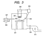
- FIG. 3 The substrate on which the zinc oxide film was formed was put in a heat treatment furnace shown in Fig. 3 for heat treatment.
- reference numeral 301 denotes a heat treatment furnace, 302, a treatment subject (the above-described substrate having the zinc oxide film formed thereon), 303, a heater, 304, a treatment furnace temperature monitoring thermocouple, and 305, a heater output adjuster.
- 306 is a heater output system, 307, a nitrogen gas mass flow controller, 308, an oxygen gas mass flow controller, 309, a pressure adjusting valve, and 310, a vacuum discharge pump.
- the substrate 302 was placed immediately below the heater 303 and the interior of the heat treatment furnace 301 was evacuated by the vacuum discharge pump 310 until the pressure was reduced to 100 Pa or lower.
- oxygen gas and nitrogen gas were introduced into the furnace while the flow rate ratio thereof was controlled by the nitrogen gas mass flow controller 307 and the oxygen gas mass flow controller 308 so that the oxygen partial pressure was set to be be 2%.
- the furnace was left standing until the pressure in the treatment furnace reached 15 kPa. As soon as the pressure 15 kPa was reached, heating was started and the treatment furnace was evacuated by controlling the pressure adjusting valve 309 so that the pressure in the treatment furnace was kept at 15 kPa during the treatment.
- the substrate was subjected to 10-minute heat treatment under the heating conditions including raising the substrate temperature to 150°C at a rate of 2.0°C/min, and then keeping the temperature at 150°C.
- the heating conditions were set by controlling the heater output by the heater output system 306.
- the heaters were turned off to cool the substrate down to room temperature while maintaining the pressure and the oxygen and nitrogen flow rate ratio so that the oxygen partial pressure was set to be be 2%.
- the substrate 302 was taken out of the heat treatment furnace 301 to measure the total reflectance and diffused reflectance, the water content of the zinc oxide film, and the electric resistance.
- the total reflectance and the diffused reflectance were measured by a spectrometer (V-570, a product of Jasco Corporation) within an optical wavelength range of 400 nm to 1200 nm.
- the water content in the film was measured by a Karl Fischer moisture titrator (MKC-510, a product of Kyoto Electronics Manufacturing Co., Ltd.).
- Metal layers (a Cr layer then an Au layer) were formed on the zinc oxide film by evaporation with the use of a vacuum evaporation apparatus and a 0.25 cm 2 mask to obtain an upper electrode, and the electric resistance between the upper electrode and the stainless steel substrate was measured.
- the electric resistance measured is considered to include an error of about 0.1 ⁇ cm 2 since a measuring system including a measuring probe itself has a circuit resistance of about 0.1 ⁇ cm 2 .
- a zinc oxide film was formed on a substrate in the same manner as in Example 1. Thereafter, the substrate 302 was put in the heat treatment furnace 301 shown in Fig. 3. The substrate was subjected to 10-minute heat treatment under the heating conditions including raising the substrate temperature to 250°C at a rate of 2. 0°C/min, and then keeping the temperature at 250°C.
- the heating conditions were set by controlling the heater output system 306.
- the heaters were turned off to cool the substrate down to room temperature while maintaining the pressure and the oxygen and nitrogen flow rate ratio so that the oxygen partial pressure was set to be be 2%.
- the substrate 302 was taken out of the heat treatment furnace 301 to measure the total reflectance and diffused reflectance, the water content of the zinc oxide film, and the electric resistance.
- a zinc oxide film was formed on a substrate in the same manner as in Example 1. Thereafter, the substrate 302 was put in the heat treatment furnace 301 shown in Fig. 3. The substrate was subjected to 10-minute heat treatment under the heating conditions including raising the substrate temperature to 300°C at a rate of 2. 0°C/min, and then keeping the temperature at 300°C.
- the heaters were turned off to cool the substrate down to room temperature while maintaining the pressure and the oxygen and nitrogen flow rate ratio so that the oxygen partial pressure was set to be be 2%.
- the substrate 302 was taken out of the heat treatment furnace 301 to measure the total reflectance and diffused reflectance, the water content of the zinc oxide film, and the electric resistance in the same manner as in Example 1.
- a zinc oxide film was formed on a substrate in the same manner as in Example 1. Thereafter, the substrate 302 was put in the heat treatment furnace 301 shown in Fig. 3. The substrate was subjected to 10-minute heat treatment under the heating conditions including raising the substrate temperature to 400°C at a rate of 2. 0°C/min, and then keeping the temperature at 400°C.
- the heaters were turned off to cool the substrate down to room temperature while maintaining the pressure and the oxygen and nitrogen flow rate ratio so that the oxygen partial pressure was set to be be 2%.
- the substrate 302 was taken out of the heat treatment furnace 301 to measure the total reflectance and diffused reflectance, the water content of the zinc oxide film, and the electric resistance in the same manner as in Example 1.
- a zinc oxide film was formed on a substrate in the same manner as in Example 1. Thereafter, the total reflectance and diffused reflectance, the water content of the zinc oxide film, and the electric resistance were measured in the same manner as in Example 1 without performing heat treatment.
- a zinc oxide film was formed on a substrate in the same manner as in Example 1. Thereafter, the substrate 302 was put in the heat treatment furnace 301 shown in Fig. 3. The substrate was subjected to 10-minute heat treatment under the heating conditions including raising the substrate temperature to 120°C at a rate of 2.0°C/min, and then keeping the temperature at 120°C.
- the heaters were turned off to cool the substrate down to room temperature while maintaining the pressure and the oxygen and nitrogen flow rate ratio so that the oxygen partial pressure was set to be be 2%.
- the substrate 302 was taken out of the heat treatment furnace 301 to measure the total reflectance and diffused reflectance, the water content of the zinc oxide film, and the electric resistance in the same manner as in Example 1.
- the semiconductor layers 104 to 106 were formed by CVD.
- the layer structure thereof is composed of an n type microcrystalline silicon ( ⁇ c-Si) film formed to a thickness of 30 nm at a temperature of 200°C, a non-doped microcrystalline silicon ( ⁇ c-Si) film formed to a thickness of 3000 nm at a temperature of 200°C, and a p type microcrystalline silicon ( ⁇ c-Si) film formed to a thickness of 10 nm at a temperature of 100°C.
- ⁇ c-Si n type microcrystalline silicon
- ⁇ c-Si non-doped microcrystalline silicon
- An ITO film was formed on the semiconductor layers to a thickness of 65 nm by deposition with the use of a sputtering device to obtain the transparent electroconductive layer 107 as an upper electrode that has an anti-reflection effect.
- a silver grid was formed on the transparent electroconductive layer by thermal evaporation to serve as the collector electrode 108, thereby completing the photovoltaic device.
- the photovoltaic device thus manufactured was measured for conversion efficiency by a solar simulator (AM 1.5, 100 mW/cm 2 , surface temperature: 25°C) for evaluation.
- the evaluation results of Examples 1 to 4 and Comparative Examples 1 and 2 are shown in Table 1.
- the water content in the zinc oxide film is obtained by measuring the water content per 8 cm 2 area of the substrate surface, converting it into a water content per 1 cm 3 of the zinc oxide film, and expressing it in mol.
- the electric resistance is an uncorrected value which includes the error due to the measurement circuit.
- the total reflectance and diffused reflectance are indicated by values at an optical wavelength of 800 nm and, if optical interference causes oscillation, by an average of values at the peaks and troughs of the oscillation.
- the conversion efficiency (Eff.) and short circuit current (Jsc) of each photovoltaic device are relative values with the conversion efficiency (Eff.) and short circuit current (Jsc) of the photovoltaic device of Comparative Example 1 set as 1.
- the zinc oxide film after the treatment is high in electric resistance and affects characteristics of the photovoltaic device. It is surmised that the characteristics of the photovoltaic device are seriously degraded by a contamination source, which results from moisture seeping from the zinc oxide film into semiconductor layers of the photovoltaic device as the semiconductor layers are formed by heating, as well as by the high electric resistance of the zinc oxide film.
- a zinc oxide film was formed on a substrate in the same manner as in Example 1. Thereafter, the substrate 302 was put in the heat treatment furnace 301 shown in Fig. 3, and was subjected to heat treatment.
- a treatment method is as follows. First, the substrate 302 was placed immediately below the heater 303 and the interior of the heat treatment furnace 301 was evacuated by the vacuum discharge pump 310 until the pressure is reduced to 100 Pa or lower. After the vacuum discharge, oxygen gas and nitrogen gas were introduced into the furnace while the flow rate ratio thereof was controlled by the nitrogen gas mass flow controller 307 and the oxygen gas mass flow controller 308 so that the oxygen partial pressure was set to be be 0.5%. As soon as the pressure 15 pKa in the treatment furnace was reached, heating was started and the treatment furnace 301 was evacuated by controlling the pressure in the treatment furnace 301 by the pressure adjusting valve 309 so that the pressure was kept at 15 kPa during the treatment.
- the substrate was subjected to 10-minute heat treatment under the heating conditions including raising the substrate temperature to 250°C at a rate of 2.0 °C/min, and then keeping the temperature at 250°C.
- the heating conditions were set by controlling the heater output by the heater output system 306.
- the heaters were turned off to cool the substrate down to room temperature while maintaining the pressure and the oxygen and nitrogen flow rate ratio so that the oxygen partial pressure was set to be be 0.5%.
- the substrate 302 was taken out of the heat treatment furnace 301 to measure the total reflectance and diffused reflectance, the water content of the zinc oxide film, and the electric resistance in the same manner as in Example 1.
- a zinc oxide film was formed on a substrate in the same manner as in Example 1. Thereafter, the substrate 302 was put in the heat treatment furnace 301 shown in Fig. 3, and was subjected to heat treatment.
- a treatment method is as follows. First, the substrate 302 was placed immediately below the heater 303 and the interior of the heat treatment furnace 301 was evacuated by the vacuum discharge pump 310 until the pressure was reduced to 100 Pa or lower. After the vacuum discharge, oxygen gas and nitrogen gas were introduced into the furnace while the flow rate ratio thereof was controlled by the nitrogen gas mass flow controller 307 and the oxygen gas mass flow controller 308 so that the oxygen partial pressure was set to be be 1.0%. The furnace was left standing until the pressure in the heat treatment furnace 301 reached 15 kPa. As soon as the pressure 15 pKa was reached, heating was started and the treatment furnace was evacuated by controlling the pressure adjusting valve 309 so that the pressure in the heat treatment furnace 301 was kept at 15 kPa during the treatment.
- the substrate was subjected to 10-minute heat treatment under the heating conditions including raising the substrate temperature to 250°C at a rate of 2.0°C/min, and then keeping the temperature at 250°C.
- the heating conditions were set by controlling the heater output by the heater output system 306.
- the heaters were turned off to cool the substrate down to room temperature while maintaining the pressure and the oxygen and nitrogen flow rate ratio in such a manner that the oxygen partial pressure was set to be be 1.0%.
- the substrate 302 was taken out of the heat treatment furnace 301 to measure the total reflectance and diffused reflectance, the water content of the zinc oxide film, and the electric resistance in the same manner as in Example 1.
- a zinc oxide film was formed on a substrate in the same manner as in Example 1. Thereafter, the substrate 302 was put in the heat treatment furnace 301 shown in Fig. 3, and was subjected to heat treatment.
- a treatment method is as follows. First, the substrate 302 was placed immediately below the heater 303 and the interior of the heat treatment furnace 301 was evacuated by the vacuum discharge pump 310 until the pressure was reduced to 100 Pa or lower. After the vacuum discharge, oxygen gas and nitrogen gas were introduced into the furnace while the flow rate ratio thereof was controlled by the nitrogen gas mass flow controller 307 and the oxygen gas mass flow controller 308 so that the oxygen partial pressure was set to be be 3.0%. The furnace was left standing until the pressure in the heat treatment furnace reached 15 kPa. As soon as the pressure 15 pKa was reached, heating was started and the treatment furnace was evacuated by controlling the pressure adjusting valve 309 so that the pressure in the heat treatment furnace 301 was kept at 15 kPa during the treatment.
- the substrate was subjected to 10-minute heat treatment under the heating conditions including raising the substrate temperature to 250°C at a rate of 2.0°C/min, and then keeping the temperature at 250°C.
- the heating conditions were set by controlling the heater output by the heater output system 306.
- the heaters were turned off to cool the substrate down to room temperature while maintaining the pressure and the oxygen and nitrogen flow rate ratio so that the oxygen partial pressure was set to be be 3.0%.
- the substrate 302 was taken out of the heat treatment furnace 301 to measure the total reflectance and diffused reflectance, the water content of the zinc oxide film, and the electric resistance in the same manner as in Example 1.
- a zinc oxide film was formed on a substrate in the same manner as in Example 1. Thereafter, the substrate 302 was put in the heat treatment furnace 301 shown in Fig. 3, and was subjected to heat treatment.
- a treatment method is as follows. First, the substrate 302 was placed immediately below the heater 303 and the interior of the heat treatment furnace 301 was evacuated by the vacuum discharge pump 310 until the pressure was reduced to 100 Pa or lower. After the vacuum discharge, oxygen gas and nitrogen gas were introduced into the furnace while the flow rate ratio thereof was controlled by the nitrogen gas mass flow controller 307 and the oxygen gas mass flow controller 308 so that the oxygen partial pressure was set to be be 5.0%. The furnace was left standing until the pressure in the heat treatment furnace reached 15 kPa. As soon as the pressure 15 pKa was reached, heating was started and the treatment furnace was evacuated by controlling the pressure adjusting valve 309 such that the pressure in the heat treatment furnace 301 was kept at 15 kPa during the treatment.
- the substrate was subjected to 10-minute heat treatment under the heating conditions including raising the substrate temperature to 250°C at a rate of 2.0°C/min, and then keeping the temperature at 250°C.
- the heating conditions were set by controlling the heater output by the heater output system 306.
- the heaters were turned off to cool the substrate down to room temperature while maintaining the pressure and the oxygen and nitrogen flow rate ratio so that the oxygen partial pressure was set to be 5.0%.
- the substrate 302 was taken out of the heat treatment furnace 301 to measure the total reflectance and diffused reflectance, the water content of the zinc oxide film, and the electric resistance in the same manner as in Example 1.
- a zinc oxide film was formed on a substrate in the same manner as in Example 1. Thereafter, the substrate 302 was put in the heat treatment furnace 301 shown in Fig. 3, and was subjected to heat treatment.
- a treatment method is as follows. First, the substrate 302 was placed immediately below the heater 303 and the interior of the heat treatment furnace 301 was evacuated by the vacuum discharge pump 310 until the pressure is reduced to 100 Pa or lower. After the vacuum discharge, oxygen gas and nitrogen gas were introduced into the furnace while the flow rate ratio thereof was controlled by the nitrogen gas mass flow controller 307 and the oxygen gas mass flow controller 308 so that the oxygen partial pressure was set to be 10.0%. The furnace was left standing until the pressure in the heat treatment furnace reached 15 kPa. As soon as the pressure 15 pKa was reached, heating was started and the treatment furnace was evacuated by controlling the pressure adjusting valve 309 such that the pressure in the heat treatment furnace 301 was kept at 15 kPa during the treatment.
- the substrate was subjected to 10-minute heat treatment under the heating conditions including raising the substrate temperature to 250°C at a rate of 2.0°C/min, and then keeping the temperature at 250°C.
- the heating conditions were set by controlling the heater output by the heater output system 306.
- the heaters were turned off to cool the substrate down to room temperature while maintaining the pressure and the oxygen and nitrogen flow rate ratio so that the oxygen partial pressure was set to be 10.0%.
- the substrate 302 was taken out of the heat treatment furnace 301 to measure the total reflectance and diffused reflectance, the water content of the zinc oxide film, and the electric resistance in the same manner as in Example 1.
- a zinc oxide film was formed on a substrate in the same manner as in Example 1. Thereafter, the substrate 302 was put in the heat treatment furnace 301 shown in Fig. 3, and was subjected to heat treatment.
- a treatment method is as follows. First, the substrate 302 was placed immediately below the heater 303 and the interior of the heat treatment furnace 301 was evacuated by the vacuum discharge pump 310 until the pressure was reduced to 100 Pa or lower. After the vacuum discharge, only nitrogen gas was introduced into the furnace. As soon as the pressure 15 pKa was reached, heating was started and the treatment furnace was evacuated by controlling the pressure adjusting valve 309 such that the pressure in the heat treatment furnace 301 was kept at 15 kPa during the treatment.
- the substrate was subjected to 10-minute heat treatment under the heating conditions including raising the substrate temperature to 250°C at a rate of 2.0°C/min, and then keeping the temperature at 250°C.
- the heating conditions were set by controlling the heater output by the heater output system 306.
- the heaters were turned off to cool the substrate down to room temperature while maintaining the pressure. Once room temperature was reached, the substrate 302 was taken out of the heat treatment furnace 301 to measure the total reflectance and diffused reflectance, the water content of the zinc oxide film, and the electric resistance in the same manner as in Example 1.
- the semiconductor layers 104 to 106 were formed by CVD.
- the layer structure thereof is composed of an n type microcrystalline silicon ( ⁇ c-Si) film formed to a thickness of 30 nm at a temperature of 150°C, a non-doped microcrystalline silicon ( ⁇ c-Si) film formed to a thickness of 3000 nm at a temperature of 200°C, and a p type microcrystalline silicon ( ⁇ c-Si) film formed to a thickness of 10 nm at a temperature of 100°C.
- ⁇ c-Si n type microcrystalline silicon
- ⁇ c-Si non-doped microcrystalline silicon
- An ITO film was formed on the semiconductor layers to a thickness of 65 nm by deposition with the use of a sputtering device to obtain the transparent electroconductive layer 107 as an upper electrode that has an anti-reflection effect.
- a silver grid is formed on the transparent electroconductive layer by thermal evaporation to serve as the collector electrode 108, thereby completing the photovoltaic device.
- the photovoltaic device thus manufactured was measured in conversion efficiency by a solar simulator (AM 1.5, 100 mW/cm 2 , surface temperature: 25°C) for evaluation.
- the evaluation results of Examples 5 to 9 and Comparative Example 3 are shown in Table 2.
- the water content in the zinc oxide film is obtained by measuring the water content per 8 cm 2 area of the substrate surface, converting it into a water content per 1 cm 3 of the zinc oxide film, and expressing it in mol.
- the electric resistance is an uncorrected value which includes the error due to the measurement circuit.
- the total reflectance and diffused reflectance are indicated by values at an optical wavelength of 800 nm and, if optical interference causes oscillation, by an average of values at the peaks and troughs of the oscillation.
- the conversion efficiency (Eff.) and short circuit current (Jsc) of each photovoltaic device are relative values with the conversion efficiency (Eff.) and short circuit current (Jsc) of the photovoltaic device of Comparative Example 1 set as 1.
- Example 5 As is clear from the results of Table 2, with the treatment condition in Example 5 (the oxygen partial pressure: 0.5%), the zinc oxide film after the treatment is low in electric resistance but is slightly reduced in reflectance. This makes Example 5 not so different from the sample subjected to heat treatment in an atmosphere that does not contain oxygen (Comparative Example 3).
- the obtained zinc oxide film exhibits fine electric characteristics and is also improved in reflectance.
- the treatment condition in Example 9 the oxygen partial pressure: 10.0%
- the obtained zinc oxide film has high electric resistance probably due to oxidation that takes place during the heat treatment, and affects characteristics of the photovoltaic device (in the form of an increase in series resistance).
- a preferable oxygen content is 1% or higher and lower than 10% in terms of partial pressure.
- Silver was deposited on a substrate in continuous form made of SUS 430 BA (thickness: 0.15 mm, width: 355 mm, length 1000 m) to a thickness of 800 nm as a metal layer by a DC magnetron sputtering apparatus capable of handling a substrate wound into a roll.
- the same DC magnetron sputtering apparatus capable of handling a roll of substrate was used to form a zinc oxide thin film by deposition on the silver layer to a thickness of 200 nm.
- a zinc oxide layer was formed on the thus prepared substrate in continuous form by the apparatus shown in Fig. 4 (apparatus for forming a continuous film on a substrate in continuous form) in a manner described below.
- the substrate in continuous form 403 was transported to the zinc oxide forming tank 405 through the transporting roller 404.
- the zinc oxide forming bath 406 contains 1 liter of water containing 70 g of zinc nitrate hexahydrate, and 0.5 g of dextrin.
- the solution in the bath was stirred through liquid circulation treatment and by an air jet injected through the air jet holes 415 which are provided in a side wall of the tank at a rate of 20 cm 3 /h.
- the temperature of the solution was kept at 85°C and its pH was so retained as to be 4.0 to 6.0 by a solution circulation system.
- the counter electrode 407 is a rectangular zinc plate having a 99.99% purity and a buffed surface.
- a current of 7.0 mA/cm 2 (0.7 A/dm 2 ) was caused to flow between the counter electrode 407 on the anode side and the substrate in continuous form 403 on the cathode side with the substrate 403 on the cathode side serving as earth.
- a zinc oxide film 2.6 ⁇ m in thickness was formed at a rate of 55 ⁇ /sec.
- the substrate was wound about a columnar bobbin core, which is 430 mm in diameter, 430 mm in width, and 10 mm in thickness, which is set in the reel-in roller 402, and which is made of stainless steel, while the meandering correction roller 414 regulated motion of the substrate.
- Thermocouples (each 0.5 mm in diameter) were inserted in the substrate roll in continuous form at points 100 m, 500 m, and 800 m from its inner end while the zinc oxide film was being formed.
- the thermocouples were provided to measure the temperature of the substrate in the subsequent heat treatment step.
- the substrate in continuous form on which the zinc oxide film was formed in the manner described above was put in the heat treatment furnace 501 shown in Figs. 5A and 5B.
- the outer end of the substrate roll was fixed before the substrate roll was held by the roll supporting posts 509.
- the interior of the heat treatment furnace 501 was evacuated by the vacuum discharge pump 503 until the pressure was reduced to 100 Pa or lower. Thereafter, nitrogen gas containing oxygen (oxygen partial pressure: 2%) was introduced into the heat treatment furnace through the gas introducing holes 510 and the pressure in the heat treatment furnace was so controlled as to be 3 kPa by the pressure adjusting valve 514 during the heat treatment.
- nitrogen gas containing oxygen oxygen partial pressure: 28% was introduced into the heat treatment furnace through the gas introducing holes 510 and the pressure in the heat treatment furnace was so controlled as to be 3 kPa by the pressure adjusting valve 514 during the heat treatment.
- the temperature in the heat treatment furnace was kept constant by monitoring the thermocouple 511 attached to the interior of the treatment furnace and controlling the heaters 505, 506, 507, and 515 through control of the output of the heater power source 513 with the use of the output controller 512.
- the heating conditions include raising the temperature to 250°C from room temperature at a rate of 2.0°C/min and keeping the temperature at 250°C for 600 minutes. Then the heaters were turned off to let the substrate cool down to room temperature in the same atmosphere as the treatment environment.
- the treatment furnace was vented and the rolled substrate was wound off to take samples at points 300 m, 600 m, and 900 m from the inner end of the substrate in continuous form roll.
- Each of the samples was measured for the total reflectance and diffused reflectance of the zinc oxide film at the ends and center in the substrate width direction, for the water content in the zinc oxide film, and for the electric resistance by a method similar to the measurement method of Example 1.
- a zinc oxide film was formed on the substrate in continuous form 403 in the manner described in Example 10, and the substrate roll 502 was then set in the heat treatment furnace 501 shown in Figs. 5A and 5B after fixing the outer end of the substrate roll.
- the interior of the heat treatment furnace 501 was evacuated by the vacuum discharge pump 503 until the pressure was reduced to 100 Pa or lower. Thereafter, nitrogen gas containing oxygen (oxygen partial pressure: 2%) was introduced into the heat treatment furnace and the pressure in the heat treatment furnace was so controlled as to be 5 kPa during the heat treatment by the pressure adjusting valve 514, which is provided in the vacuum discharge system. The rest of the conditions in the heat treatment were identical to those in Example 10. Then the substrate on which the zinc oxide film was formed was measured for the total reflectance and diffused reflectance, the water content in the zinc oxide film, and the electric resistance.
- a zinc oxide film was formed on the substrate in continuous form 403 in the manner described in Example 10, and the substrate roll 502 was then set in the heat treatment furnace 501 shown in Figs. 5A and 5B after fixing the outer end of the substrate roll.
- the interior of the heat treatment furnace 501 was evacuated by the vacuum discharge pump 503 until the pressure was reduced to 100 Pa or lower. Thereafter, nitrogen gas containing oxygen (oxygen partial pressure: 2%) was introduced into the heat treatment furnace and the pressure in the heat treatment furnace was so controlled as to be 15 kPa during the heat treatment by the pressure adjusting valve 514, which is provided in the vacuum discharge system. The rest of the conditions in the heat treatment were identical to those in Example 10. Then the substrate on which the zinc oxide film was formed was measured for the total reflectance and diffused reflectance, the water content in the zinc oxide film, and the electric resistance.
- a zinc oxide film was formed on the substrate in continuous form 403 in the manner described in Example 10, and the substrate roll 502 was then set in the heat treatment furnace 501 shown in Figs. 5A and 5B after fixing the outer end of the substrate roll.
- the interior of the heat treatment furnace 501 was evacuated by the vacuum discharge pump 503 until the pressure was reduced to 100 Pa or lower. Thereafter, nitrogen gas containing oxygen (oxygen partial pressure: 2%) was introduced into the heat treatment furnace and the pressure in the heat treatment furnace was so controlled as to be 50 kPa during the heat treatment by the pressure adjusting valve 514, which is provided in the vacuum discharge system. The rest of the conditions in the heat treatment were identical to those in Example 10. Then the substrate on which the zinc oxide film was formed was measured for the total reflectance and diffused reflectance, the water content in the zinc oxide film, and the electric resistance.
- a zinc oxide film was formed on the substrate in continuous form 403 in the manner described in Example 10, and the substrate roll 502 was then set in the heat treatment furnace 501 shown in Figs. 5A and 5B after fixing the outer end of the substrate roll.
- the interior of the heat treatment furnace 501 was evacuated by the vacuum discharge pump 503 until the pressure was reduced to 100 Pa or lower. Thereafter, nitrogen gas containing oxygen (oxygen partial pressure: 2%) was introduced into the heat treatment furnace and the pressure in the heat treatment furnace was so controlled as to be 75 kPa during the heat treatment by the pressure adjusting valve 514, which is provided in the vacuum discharge system. The rest of the conditions in the heat treatment were identical to those in Example 10. Then the substrate on which the zinc oxide film was formed was measured for the total reflectance and diffused reflectance, the water content in the zinc oxide film, and the electric resistance.
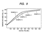
- Tables 3 to 5 show results of measuring the substrates on which the zinc oxide films are formed in Examples 10 to 14.
- the measurement results in Tables 3 to 5 are for measurements taken at points 300 m, 600 m, and 900 m from the bobbin core in the longitudinal direction of the substrates.
- the appropriate pressure range in heat treatment for a substrate in continuous form wound into a roll is 5 kPa or higher and lower than 50 kPa.
- Silver was deposited on a substrate in continuous form made of SUS 430 BA (thickness: 0.15 mm, width: 355 mm, length 1000 m) to a thickness of 800 nm as a metal layer by a DC magnetron sputtering apparatus capable of handling a substrate wound into a roll.
- the same DC magnetron sputtering apparatus capable of handling a roll of substrate was used to form a zinc oxide thin film by deposition on the silver layer to a thickness of 200 nm.
- a zinc oxide layer was formed on the thus prepared substrate in continuous form by the apparatus shown in Fig. 4 (apparatus for forming a continuous film on a substrate in continuous form) in a manner described below.
- the substrate in continuous form 403 was transported to the zinc oxide forming tank 405 through the transporting roller 404.
- the zinc oxide forming bath 406 contained 1 liter of water containing 70 g of zinc nitrate hexahydrate, and 0.5 g of dextrin.
- the solution of the bath was stirred through liquid circulation treatment and by an air jet injected through the air jet holes 415 which are provided in a side wall of the tank at a rate of 20 cm 3 /h.
- the temperature of the solution is kept at 85°C and its pH was so retained as to be 4.0 to 6.0 by a solution circulation system.
- the counter electrode 407 is a rectangular zinc plate having a 99.99% purity and a buffed surface.
- a current of 7.0 mA/cm 2 (0.7 A/dm 2 ) was caused to flow between the counter electrode 407 on the anode side and the substrate in continuous form 403 on the cathode side with the substrate 403 on the cathode side serving as earth.
- a zinc oxide film 2.6 ⁇ m in thickness was formed at a rate of 55 ⁇ /sec.
- the substrate was wound about a columnar bobbin core, which is 430 mm in diameter, 430 mm in width, and 10 mm in thickness, which is set in the reel-in roller 402, and which is made of stainless steel, while the meandering correction roller 414 regulated motion of the substrate.
- a columnar bobbin core which is 430 mm in diameter, 430 mm in width, and 10 mm in thickness, which is set in the reel-in roller 402, and which is made of stainless steel, while the meandering correction roller 414 regulated motion of the substrate.
- the substrate in continuous form on which the zinc oxide film was formed in the manner described above was put in the heat treatment furnace 501 shown in Figs. 5A and 5B.
- the outer end of the substrate roll was fixed before the substrate roll was held by the roll supporting posts 509.
- the interior of the heat treatment furnace 501 was evacuated by the vacuum discharge pump 503 until the pressure was reduced to 100 Pa or lower. Thereafter, nitrogen gas containing oxygen (oxygen partial pressure: 2%) was introduced into the heat treatment furnace through the gas introducing holes 510 and the pressure in the heat treatment furnace was controlled to 3 kPa by the pressure adjusting valve 514 during the heat treatment.
- nitrogen gas containing oxygen oxygen partial pressure: 28% was introduced into the heat treatment furnace through the gas introducing holes 510 and the pressure in the heat treatment furnace was controlled to 3 kPa by the pressure adjusting valve 514 during the heat treatment.
- the temperature in the heat treatment furnace was kept constant by monitoring the thermocouple 511 attached to the interior of the treatment furnace and controlling the heater output with the use of the heater output controller 512.
- the heating conditions include raising the temperature to 250°C from room temperature at a rate of 2.0°C/min and keeping the temperature at 250°C for 600 minutes. Then the heaters were turned off to allow the substrate to cool down to room temperature in the same atmosphere as the treatment environment.
- the treatment furnace was vented and the rolled substrate was wound off to take samples at points 300 m, 600 m, and 900 m from the inner end of the substrate in continuous form roll. Then, deformation of the substrate was evaluated.
- the deformation was evaluated by placing a sample substrate on a table or the like with a flat surface and measuring a height Z (longitudinal direction: x, width direction: y, height direction: z) of a waved portion at each end of the sample substrate as shown in Fig. 6.
- a zinc oxide film was formed on a substrate in continuous form in the manner described in Example 15 and the substrate was similarly wound into a roll to be held by the roll supporting posts 509 in the heat treatment furnace 501 shown in Figs. 5A and 5B.
- the heating conditions include raising the temperature to 250°C from room temperature at a rate of 5.0°C/min and keeping the temperature at 250°C for 600 minutes. Then the heaters were turned off to allow the substrate to cool down to room temperature in the same atmosphere as the treatment environment.
- the treatment furnace was vented and the rolled substrate was wound off to take samples at points 300 m, 600 m, and 900 m from the inner end of the substrate in continuous form roll. Then, deformation of the substrate was evaluated in the same manner as in Example 1.
- the results show that the substrate in continuous form was deformed at ends in the width direction when the temperature is raised at a rate faster than 2.0°C/min during heat treatment. This is because the heaters heat the substrate roll in continuous form from the outer folds of the roll to bring about a large temperature difference between the roll core and the roll surface and, accordingly, deformation of the substrate.
- Silver was deposited on a substrate in continuous form made of SUS 430 BA (thickness: 0.15 mm, width: 355 mm, length 700 m) to a thickness of 800 nm as a metal layer by a DC magnetron sputtering apparatus capable of handling a substrate wound into a roll.
- the same DC magnetron sputtering apparatus capable of handling a roll of substrate was used to form a zinc oxide thin film by deposition on the silver layer to a thickness of 200 nm.
- a zinc oxide layer was formed on the thus prepared substrate in continuous form by the apparatus shown in Fig. 4 (apparatus for forming a continuous film on a substrate in continuous form) in a manner described below.
- the substrate in continuous form 403 was transported to the zinc oxide forming tank 405 through the transporting roller 404.
- the zinc oxide forming bath 406 contained 1 liter of water containing 70 g of zinc nitrate hexahydrate, and 0.5 g of dextrin.
- the solution of the bath was stirred through liquid circulation treatment and by an air jet injected through the air jet holes 415 which are provided in a side wall of the tank at a rate of 20 cm 3 /h.
- the temperature of the solution was kept at 85°C and its pH was so retained as to be 4.0 to 6.0 by a solution circulation system.
- the counter electrode 407 is a rectangular zinc plate having a 99.99% purity and a buffed surface.
- a current of 7.0 mA/cm 2 (0.7 A/dm 2 ) was caused to flow between the counter electrode 407 on the anode side and the substrate in continuous form 403 on the cathode side with the substrate 403 on the cathode side serving as earth.
- a zinc oxide film 2.6 ⁇ m in thickness was formed at a rate of 55 ⁇ /sec.
- the substrate was wound about a columnar bobbin core, which is 430 mm in diameter, 430 mm in width, and 10 mm in thickness, which is set in the reel-in roller 402, and which is made of stainless steel, while the meandering correction roller 414 regulated motion of the substrate.
- a columnar bobbin core which is 430 mm in diameter, 430 mm in width, and 10 mm in thickness, which is set in the reel-in roller 402, and which is made of stainless steel, while the meandering correction roller 414 regulated motion of the substrate.
- the substrate in continuous form on which the zinc oxide film was formed in the manner described above was put in the heat treatment furnace 501 shown in Figs. 5A and 5B.
- the outer end of the substrate roll was fixed before the substrate roll was held by the roll supporting posts 509.
- the interior of the heat treatment furnace 501 was evacuated by the vacuum discharge pump 503 until the pressure was reduced to 100 Pa or lower. Thereafter, nitrogen gas containing oxygen (oxygen partial pressure: 2%) was introduced into the heat treatment furnace and the pressure in the heat treatment furnace was so controlled as to be 15 kPa by the pressure adjusting valve 514 during the heat treatment.
- the temperature in the heat treatment furnace was kept constant by monitoring the thermocouple 511 attached to the interior of the treatment furnace and controlling the heater output with the use of the output controller 512.
- the heating conditions include raising the temperature to 250°C from room temperature at a rate of 2.0°C/min and keeping the temperature at 250°C for 500 minutes. Then the heaters were turned off to let the substrate cool down to room temperature in the same atmosphere as the treatment environment.
- Example 15 After the substrate was cooled down, the treatment furnace was vented and the rolled substrate was wound off to take samples at points 300 m and 600 m from the inner end of the substrate in continuous form roll. Each of the samples was measured for the total reflectance and diffused reflectance of the zinc oxide film at the ends and center in the substrate width direction, for the water content in the zinc oxide film, and for the electric resistance by a method similar to the measurement method of Example 1. Further, deformation of the substrate was evaluated in the same manner as in Example 15.
- a zinc oxide film was formed on a substrate in continuous form at a point 1500 m in the manner described in Example 17 and the substrate was similarly wound into a roll to be held by the roll supporting posts 509 in the heat treatment furnace 501 shown in Figs. 5A and 5B.
- the heating conditions include raising the temperature to 250°C from room temperature at a rate of 2.0°C/min and keeping the temperature at 250°C for 960 minutes. Then the heaters are turned off to let the substrate cool down to room temperature in the same atmosphere as the treatment environment.
- Example 15 After the substrate was cooled down, the treatment furnace was vented and the rolled substrate was wound off to take samples at points 300 m, 600 m, 900 m, and 1200 m from the inner end of the substrate in continuous form roll. Each of the samples was measured for the total reflectance and diffused reflectance of the zinc oxide film at the ends and center in the substrate width direction, for the water content in the zinc oxide film, and for the electric resistance by a method similar to the measurement method of Example 1. Further, deformation of the substrate was evaluated in the same manner as in Example 15.
- Results of Examples 17 and 18 are shown in Tables 7 to 10 (the tables also include the results of Example 12 for comparison).
- Table 7 the water content in the zinc oxide film is obtained by measuring the water content per 8 cm 2 area of the substrate surface, converting it into a water content per 1 cm 3 of the zinc oxide film, and expressing it in mol.
- the electric resistance shown in Table 8 is an uncorrected value which includes the error due to the measurement circuit.
- the total reflectance and diffused reflectance shown in Table 9 are indicated by values at an optical wavelength of 800 nm and, if optical interference causes oscillation, by the average of values at the peaks and troughs of the oscillation.
- Table 10 shows substrate deformation, and the circular symbol (O) indicates that the wave height at an end of the substrate is 1.0 mm or less, the triangular symbol ( ⁇ ) indicates that the wave height is 1. 0 to 1.5 mm, and the symbol X indicates that the wave height is 1.5 mm or more.
- heat treatment under heat treatment conditions according to the present invention provides a zinc oxide film formed on a substrate with uniform characteristics throughout the length of the substrate, and that the water content of the zinc oxide film can be reduced even when the substrate is a substrate in continuous form and wound into a roll during the heat treatment.
- a substrate in continuous form of any length can be employed without losing uniform characteristics of a zinc oxide film and without suffering from substrate deformation by simply adjusting the length of the heating time.
- the present invention is not limited thereto.
- the present invention is applicable to other types of photovoltaic devices, for example, a dye-sensitized solar cell.
- existing methods can be employed for manufacture of portions of the cell that are not relevant to the zinc oxide film.
- a zinc oxide film treatment method of the present invention is capable of controlling the water content in a zinc oxide film, lowering the electric resistance of the zinc oxide film, and preventing lowering of the total reflectance and diffused reflectance which is accompanied by reduction in water content of the zinc oxide film by heat treatment.
- the present invention can also improve the photoelectric conversion efficiency of a photovoltaic device by treating a zinc oxide film by the treatment method of the present invention and forming semiconductor layers of the photovoltaic device on the zinc oxide film at a temperature lower than the heat treatment temperature of the zinc oxide film.
- a film of zinc oxide electrochemically deposited from an aqueous solution is subjected to heat treatment at a temperature equal to or higher than 150°C and equal to or lower than 400°C in a nitrogen or inert gas atmosphere that contains oxygen, thereby obtaining a zinc oxide film that is low in electric resistance without impairing the light transmittance of the zinc oxide film.
Abstract
A film of zinc oxide electrochemically
deposited from an aqueous solution is subjected to
heat treatment at a temperature equal to or higher
than 150°C and equal to or lower than 400°C in a
nitrogen or inert gas atmosphere that contains oxygen,
thereby obtaining a zinc oxide film that is low in
electric resistance without impairing the light
transmittance of the zinc oxide film.
Description
The present invention relates to a method of
treating a zinc oxide film that is formed by
electrochemical deposition, a method of manufacturing
a photovoltaic device utilizing the same, and a zinc
oxide film treatment apparatus.
Photovoltaic devices including hydrogenated
amorphous silicon, hydrogenated amorphous silicon
germanium, hydrogenated amorphous silicon carbide,
microcrystalline silicon, or polycrystalline silicon,
are conventionally provided with back side reflection
layers in order to improve light-collection
efficiency in the long-wavelength regions. Such
reflection layers desirably show effective reflection
characteristics at wavelengths which are close to
band edges of semiconductor materials and at which
absorption becomes small, i.e., wavelengths of 800 nm
to 1,200. Those that can fulfill such conditions are
reflection layers formed of a metal such as gold,
silver, copper, or aluminum, or alloys thereof. Also,
the following attempt, which is known as the light
entrapment experiment, has been done: an irregular
transparent electroconductive layer, which is
optically transparent, is provided within a
predetermined wavelength region so that reflected
light can effectively be utilized to improve short-circuit
current density Jsc. Further, the
transparent conductive layer also prevents
characteristics from deteriorating owing to shunt
pass. In most general cases, those layers are
deposited by a process such as vacuum evaporation or
sputtering and show an improvement in short-circuit
current density.
As an example thereof, in "Light Entrapment
Effect in a-SiGe Solar Cells on 29p-MF-22 Stainless
Steel Substrates" (Autumn, 1990), The 51st Applied
Physics Society Scientific Lecture Meeting, Lecture
Drafts p.747, "P-IA-15a-SiC/a-Si/a-SiGe Multi-Bandgap
Stacked Solar Cells with Bandgap Profiling",
Sannomiya et al., Technical Digest of The
International PVSEC-5, Kyoto, Japan, p.381, 1990,
reflectance and texture structure are studied on a
reflection layer constituted of silver atoms. In
this example, it is reported that the reflection
layer is deposited in double layer of silver by
changing the substrate temperature, to form effective
irregularities, and an increase in short-circuit
current in virtue of light entrapment effect has been
achieved by combination with the zinc oxide layer.
Japanese Patent No. 3273294 discloses that a
zinc oxide film formed from a zinc oxide film
manufacturing electrolytic solution, which is
composed of an aqueous solution containing 0.001
mol/l to 0.t mol/l of zinc ions and 0.001 mol/l to
0.5 mol/l of nitrate ions, is uniform in thickness
and composition and has excellent optical
transparency.
Japanese Patent Application Laid-Open No. H10-140373
discloses a zinc oxide thin film manufacturing
method which includes a step of forming a first zinc
oxide thin film on a substrate by sputtering and a
step of immersing the substrate in an aqueous
solution that contains at least nitrate ions, zinc
ions, and carbohydrate to form a second zinc oxide
thin film on the first zinc oxide thin film by
causing a current to flow between the substrate and
an electrode that is immersed in the solution.
According to this manufacturing method, a zinc oxide
thin film that shows excellent adhesion to a
substrate can be formed at low costs without causing
abnormal growth of the film.
Japanese Patent Application Laid-open No. 2001-152390
discloses that a zinc oxide film formed from a
zinc oxide film manufacturing electrolytic solution
that is composed of an aqueous solution has high
electric resistance owing to water absorbed in the
zinc oxide film but is reduced in resistance when
dried by heating. Also disclosed in Japanese Patent
Application Laid-Open No. 2002-237606 is that a solar
cell obtained by forming a semiconductor layer on a
zinc oxide film whose water content is 7.5 × 10⁻³
mol/cm3 or lower is improved in photoelectric
conversion efficiency.
However, when a photovoltaic device is
manufactured by forming a semiconductor layer on a
zinc oxide thin film that is placed on a metal layer,
a back side reflection layer of high reflectance is
indispensable for further improvement in
photoelectric conversion efficiency. To improve the
photoelectric conversion efficiency, in particular,
short circuit current, of a photovoltaic device
having as a back side reflection layer a zinc oxide
film that is formed by depositing on a silver,
aluminum, copper, or like other metal thin film on a
substrate, the back side metal layer should reflect
an increased amount of light toward a semiconductor
layer of the photovoltaic device by reducing light
absorption of the zinc oxide film which is formed by
deposition on the metal layer. If the electric
resistance of the zinc oxide film is optimized at the
same time, the short circuit current value of the
photovoltaic device and the curved factor can be
improved even more. Japanese Patent Application
Laid-Open No. 2002-237606 points out that reduction
in water content of a zinc oxide film slightly lowers
the reflectance of the film while the electric
resistance of the film is reduced.
It is also preferable for improvement in
photoelectric conversion efficiency, short circuit
current, in particular, of a photovoltaic device to
elongate an optical path by surface irregularities on
a back side reflection layer. One method to achieve
this is to thicken a zinc oxide film of the
photovoltaic device. In this case, however, the
electric resistance of the zinc oxide film could be
raised owing to the water content of the zinc oxide
film (on the premise that a thicker zinc oxide film
contains more water) and a contamination source could
be created by steam expelled from a substrate when
the substrate is heated in a later step
(semiconductor deposition step).
In addition, its manufacture process needs to
shorten the treatment time of a heat treatment step,
uniformize characteristics throughout a large-area
substrate region, and reduce the cost of a treatment
apparatus.
The present invention has been made in view of
the above circumstances, and a main object of the
present invention is therefore to provide with higher
productivity a zinc oxide film for use as a back side
reflection layer which is improved in light
reflectance while reduced in electric resistance and
which has optimum characteristics as a substrate for
a photovoltaic device.
According to the present invention, there is
provided a deposition film (zinc oxide film)
treatment method for heating a film of zinc oxide
electrochemically deposited on an electroconductive
substrate from an aqueous solution, the method being
characterized in that a treatment temperature is set
to 150°C or higher and 400°C or lower, and that the
heat treatment employs a N2 or inert gas atmosphere
that contains oxygen.
The zinc oxide film treatment method according
to the present invention described above further
includes the following preferable characteristics:
The zinc oxide film treatment method of the
present invention is capable of controlling the water
content in a zinc oxide film so that it falls within
an optimum range. The water content in a zinc oxide
film is preferably 7.5 × 10⁻³ mol/cm3 or less, more
preferably 5.0 × 10⁻³ mol/cm3 or less. With the water
content confined in this range, a zinc oxide film can
have low electric resistance. Although the mechanism
is not exactly clear at present, what has been found
is that lowering of the total reflectance and
diffused reflectance of a zinc oxide film (considered
as lowering of transmittance of the zinc oxide film
due to lack of oxygen in the zinc oxide film) which
is usually accompanied by reduction in water content
of the zinc oxide film by heat treatment is avoided
by subjecting the zinc oxide film to heat treatment
in an inert gas atmosphere that contains oxygen,
preferably, in a treatment atmosphere where the
oxygen partial pressure ratio is 1% or more and less
than 10%. In this way, lowering of the transmittance
of the zinc oxide film can be prevented from lowering
to improve the total reflectance and diffused
reflectance of the film.
Furthermore, the treatment apparatus can be
simplified by subjecting a substrate in continuous
form to heat treatment with the substrate wound into
a roll. Moreover, stress generated during the heat
treatment in the zinc oxide film along the length of
the substrate in continuous form is reduced by
keeping the treatment pressure preferably less than
50 kPa, more preferably 5 kPa or more and less than
50 kPa. Thus the zinc oxide film can receive uniform
treatment without deformation of the substrate in
continuous form.
Further, according to the present invention,
there is provided a method of manufacturing a
photovoltaic device, characterized by including a
step of forming, on a zinc oxide film heated by a
zinc oxide film treatment method according to the
present invention described above, semiconductor
layers at a temperature lower than the treatment
temperature.
Further, according to the present invention,
there is provided a zinc oxide film treatment
apparatus for heating, at a pressure equal to or
lower than an atmospheric pressure, a film of zinc
oxide electrochemically deposited on an
electroconductive substrate from an aqueous solution,
the apparatus characterized by including: exhaust
means for reducing the pressure in a treatment
chamber to the atmospheric pressure or lower; heating
means for heating the deposition film; and gas
introducing means for introducing, into the treatment
chamber, N2 or inert gas that contains oxygen.
The zinc oxide film treatment apparatus
according to the present invention described above
includes the following preferable characteristics:
A zinc oxide film treatment method of the
present invention is suitable for treatment of such a
zinc oxide film that is formed from a zinc oxide film
manufacturing electrolytic solution composed of an
aqueous solution on a substrate in continuous form
(e.g., SUS 430 2D), on which a metal layer (silver,
aluminum or copper, or an alloy thereof) and another
zinc oxide film are formed in advance by sputtering
and layered with the zinc oxide film on top of the
metal layer.
Described below are effects brought about by
characteristics of the present invention.
The present invention is characterized by
subjecting an electroconductive substrate, on which a
zinc oxide film is formed by deposition from an
aqueous solution, to heat treatment within a given
temperature range under a N2 or inert gas atmosphere
that contains oxygen. As indicated in Japanese
Patent Application Laid-Open No. 2002-237606,
excessive moisture or oxygen adsorbed in any zinc
oxide film affects electric characteristics of the
film irrespective of the method employed to form the
film and causes problems when the film is used as a
back side reflection layer of a photovoltaic device,
for example.
On the other hand, an appropriate amount of
moisture in a zinc oxide film can give the film an
improved transmittance. Specifically, a zinc oxide
film having a proper water content exhibits high
reflectance as a back side reflection layer of a
photovoltaic device and improves the photoelectric
conversion efficiency (in particular, short circuit
current) of the device.
According to the present invention, the water
content in a zinc oxide film is reduced by heat
treatment to obtain better electric characteristics
and the reflectance characteristics, which would be
degraded by heat treatment in prior art, are improved.
Heat treatment lowers the electric resistance
of a zinc oxide film and its transmittance as well.
Although the mechanism thereof is not exactly clear
at present, it is surmised that reduction in water
content of the film by heat treatment removes oxygen
from the weak oxygen-zinc bond, making the film
slightly rich with zinc and thereby giving the film
better electric characteristics while lowering the
film's light transmittance.
In contrast, the heat treatment method
according to the present invention selectively
removes water from a zinc oxide film and limits the
oxygen desorption reaction during heat treatment.
The prevention of oxygen desorption, or re-oxidation
of a portion where oxygen desorption has taken place
once, is made possible by the presence of a very
small amount of oxygen in the treatment atmosphere,
specifically, less than 10% partial pressure ratio of
oxygen introduced into the treatment atmosphere, and
the light transmittance of the zinc oxide film is
thus maintained. The inventors of the present
invention have confirmed that the once-lowered
transmittance of a zinc oxide film can be recovered
by heating the film in an atmosphere that contains
oxygen, and this confirmation explains how oxidation
of a zinc oxide film improves the light transmittance
of the film.
Next, a mode of carrying out the present
invention is described with reference to the
accompanying drawings.
Fig. 1 is a representative schematic sectional
view of a photovoltaic device according to the
present invention. In Fig. 1, Reference Symbol 101
denotes a substrate (support member); 102, a metal
layer (back side reflection layer); and 103, a zinc
oxide layer composed of hexagonal polycrystals.
Denoted by 104, 105, and 106 are semiconductor layers.
Reference Symbol 107 represents a transparent
electroconductive layer; and 108, a collector
electrode. In a structure in which light enters from
a transparent substrate, those layers excluding the
substrate are formed in the reverse order.
The substrate 101 is a metal layer or a resin,
glass, ceramic, or like other substrate coated with
an electroconductive material. The substrate 101 may
have minute surface irregularities. A transparent
substrate may be employed as the substrate 101 so
that light enters from the substrate side. If the
substrate 101 is in continuous form, a zinc oxide
film can be formed continuously. In this case, a
flexible material such as stainless steel or
polyimide is particularly preferable for the
substrate 101.
The metal layer 102 serves as an electrode and
as a reflection layer for reflecting light that has
reached the substrate 101 in order to reuse the light
in the semiconductor layers. The metal layer is
formed from Al, Cu, Ag, Au, or the like by
evaporation, sputtering, electrolytic deposition,
printing, or other methods. The metal layer can be
omitted if the substrate is electroconductive.
The metal layer 102 preferably has surface
irregularities, so that an optical path of the
reflected light is elongated in the semiconductor
layers and the short circuit current is accordingly
increased.
The zinc oxide layer 103 increases diffuse
reflection of incident light and of reflected light
to elongate their optical path lengths in the
semiconductor layers. The zinc oxide layer 103 also
prevents elements of the metal layer 102 from
diffusing or migrating into the semiconductor layers
to cause the photovoltaic device to shunt. In
addition, with its resistance set appropriately, the
zinc oxide layer 103 prevents short circuit due to
pinholes and like other defects of the semiconductor
layers. Similarly to the metal layer 102, the zinc
oxide layer 103 preferably has surface irregularities.
The zinc oxide layer 103 is formed by an
electrolytic deposition method described below. It
is more preferable to form a zinc oxide film on the
metal layer 102 by sputtering or the like before
another zinc oxide film is formed on the former zinc
oxide film by electrolytic deposition. This is
because the adhesion between the metal layer 102 and
the zinc oxide layer 103 is improved.
For example, an apparatus shown in Fig. 2 can
be used to form the zinc oxide layer 103. In Fig. 2,
Reference Symbol 201 denotes an anti-corrosion
vessel; 202, an electrolytic deposition aqueous
solution; 203, an electroconductive substrate; 204, a
counter electrode; 205, a power source; 206, a load
resistor; 207, a substrate supporting shaft; and 208,
an electrode supporting shaft.
The electrolytic deposition aqueous solution
202 is an aqueous solution containing at least zinc
ions and nitrate ions, and saccharose or dextrin.
The zinc ion concentration is preferably 0.002 mol/l
to 3.0 mol/l, more preferably 0.01 mol/l to 1.5 mol/l,
optimally 0.05 mol/l to 0.7 mol/l. The nitrate ion
concentration is preferably 0.004 mol/l to 6.0 mol/l,
more preferably 0.01 mol/l to 1.5 mol/l, optimally
0.1 mol/l to 1.4 mol/l. The saccharose concentration
is preferably 1 g/l to 500 g/l, more preferably 3 g/l
to 100 g/l. The dextrin concentration is preferably
0.01 g/l to 10 g/l, more preferably 0.025 g/l to 1
g/l. With the use of an aqueous solution having the
above concentrations, a zinc oxide thin film of a
texture structure suitable for the light entrapment
effect can be formed efficiently.
The electroconductive substrate 203 is the
substrate 101 on which the metal layer 102 is formed.
The counter electrode 204 is made from a zinc plate
with its surface buffed, and serves as an anode. The
zinc content of the zinc plate is preferably 90% or
higher, more preferably 99% or higher.
The counter electrode 204 is controlled in a
manner that a constant current is allowed to flow.
The current value thereof is preferably 0.1 mA/cm2 to
100 mA/cm2, more preferably 1 mA/cm2 to 30 mA/cm2,
optimally 3 mA/cm2 to 15 mA/cm2.
The semiconductor layers 104, 105, and 106 are
formed from amorphous or microcrystalline Si, C, or
Ge, or an alloy thereof. The semiconductor layers
also contain hydrogen and/or halogen atoms. A
preferable content of hydrogen and/or halogen atoms
is 0.1 through 40 atm%. The semiconductor layers may
additionally contain oxygen, nitrogen, and the like.
The concentration of these impurities is desirably 5
× 1019 /cm3 or less. The semiconductor layers also
contain an element belonging to Group III in order to
obtain the p-type conductivity and an element
belonging to Group V in order to obtain the n-type
conductivity.
In the case of a stacked cell, a semiconductor
layer of an i type of a pin junction near the light
incident side is wide in band gap. The band gap
preferably becomes narrower for a farther pin
junction. The local minimal value of the band gap is
preferably located nearer to the p layer than the
middle of the thickness of the i layer.
For a doped layer on the light incident side, a
crystalline semiconductor that absorbs light in a
smaller quantity or a semiconductor having a wide
band gap is suitable.
Microwave (MW) plasma CVD or radio frequency
(RF) CVD is a method suitable for forming the
semiconductor layers.
An example of a deposition technique that can
be employed to form the semiconductor layers is
disclosed in Japanese Patent Application Laid-Open No.
04-119843 in which an i layer is formed of graded
SiGe and has a Ge composition ratio of 20 to 70 atm%.
The transparent electrode layer 107 can double
as an anti-reflection layer if set to an appropriate
thickness. ITO, ZnO, In2O3, or like other material is
used to form the transparent electrode layer by
evaporation, CVD, spraying, spin-on, immersion, etc.
A substance that causes a change in electric
conductivity may be added to those compounds.
The collector electrode 108 is provided to
improve the current collection efficiency. The
collector electrode 108 can be obtained by forming a
metal film into a current collection pattern by
sputtering with the use of a mask, or by printing
with an electroconductive paste or solder paste as
ink, or by fixing a metal wire with an
electroconductive paste.
If necessary, a protective layer is formed on
each side of the photovoltaic device. A reinforcing
member such as a steel plate may be employed at the
same time.
A description is given concerning how a zinc
oxide film is formed by deposition with reference to
Fig. 4, which shows an apparatus for forming a
continuous film on a substrate in continuous form.
In Fig. 4, Reference Symbol 401 denotes a feeding
roller; 402, a reel-in roller; 403, a substrate in
continuous form; 404, a transporting roller; 405, a
zinc oxide forming tank; 406, a zinc oxide forming
bath; 407, a counter electrode; 408, a DC power
source; 409, a washing tank; 410, a pure water
washing tank; 411, a pure water shower; 412, a drying
furnace; 413, air holes; 414, a meandering correction
roller; and 415, air jet holes.
The substrate in continuous form 403 wound
around the feeding roller 401 is transported along a
path shown in Fig. 4 and is reeled onto the reel-in
roller 402 while a slight positional displacement of
the substrate is corrected by the meandering
correction roller 414.
The zinc oxide forming bath 406 of the zinc
oxide forming tank 405 is the above-described
electrolytic deposition aqueous solution which
contains nitrate ions, zinc ions, and saccharose or
dextrin.
The counter electrode 407 has one or more
square-shaped zinc plates with a 99.99% purity. The
DC power source 408 is controlled to apply voltages
in a manner that the substrate in continuous form 403
is made to be a cathode and the counter electrode 407
is made to be an anode and to cause a constant
current flow.
The temperature of the electrolytic deposition
aqueous solution is set to 50°C or higher. An
appropriate amount of air from an air injection pump
(not shown in the drawing) is injected into the bath
through the air jet holes 415, which are provided in
a side wall of the zinc oxide forming tank to stir
the bath. In this way, a uniform zinc oxide film
with reduced abnormal growth can be formed
efficiently.
An example of a heat treatment apparatus
according to the present invention is shown in Figs.
5A (front view) and 5B (side view). In Figs. 5A and
5B, Reference Symbol 501 denotes a heat treatment
furnace (treatment chamber); 502, a treatment subject
(substrate in continuous form); 503, a vacuum
discharge pump; 504, a trap; 505, a side heater unit;
506, a front heater unit; 507, rear heater unit; 508,
reflection plates; 509, bobbin supporting posts; 510,
gas introducing holes; 511, a temperature monitoring
thermocouple; 512, a heater output controller; 513, a
heater power source; 514, a pressure adjusting valve;
and 515, a central heater unit.
A zinc oxide film is formed on the substrate in
continuous form 502 by the apparatus shown in Fig. 4
(an apparatus for forming a continuous film on a
substrate in continuous form). The substrate is
wound around a bobbin made of stainless steel and the
bobbin is held by the two bobbin supporting posts 509
set in the reflection plates 508.
The interior of the treatment chamber 501 is
evacuated by the vacuum discharge pump 503 and the
pressure adjusting valve 514 to set the pressure in
the chamber to 100 Pa or lower. After the vacuum
discharge, nitrogen and oxygen are introduced into
the chamber while the flow rate thereof is controlled
by a mass flow controller (not shown in the drawing)
until a desired pressure level is reached. The
treatment subject 502 is heated by the side, front,
and rear heater units 505 to 507 installed on the
reflection plates 508 and by the central heater unit
515 set in the center of the treatment subject 502.
The temperature in the treatment chamber is set to a
desired level by monitoring the temperature gauge
(hollow thermocouple) 511 and controlling the output
of the heater power source 513 through the heater
output controller 512. After the heat treatment is
completed, the treatment subject is cooled down to
room temperature while the conditions and atmosphere
used in the heat treatment are maintained.
Examples of the present invention are described
below but the present invention is not limited to the
following Examples. In particular, a mixture gas of
oxygen and nitrogen used as atmosphere gas during
heat treatment in the following Examples can be
replaced by a mixture gas of oxygen and inert gas
such as helium or argon.
In this example, a zinc oxide film was formed
with the use of an electrodeposition apparatus as the
one shown in Fig. 2 and was subjected to heat
treatment.
The electroconductive substrate 203 on the
cathode side was prepared by forming a silver film
with a thickness of 800 nm on a 50-mm square
stainless steel plate 430 BA having a thickness of
0.15 mm. The silver film was formed by a sputtering
apparatus (ULVAC SBH-2206DE) in an argon atmosphere
through application of a constant current of 0.3 A
with the pressure set to 0.399 Pa and the temperature
set to 350°C. The counter electrode 204 on the anode
side was a 40-mm square zinc plate having a 99.99%
purity and a thickness of 1.2 mm. The distance
between the counter electrode 204 and the
electroconductive substrate 203 was fixed and set to
50 mm.
The aqueous solution 202 was prepared by adding
12 g/l of saccharose to 0.15 mol/l of zinc nitrate
having a temperature of 80°C. The solution was
stirred by a stirrer 214. The current of 3.0 mA/cm2
(0.3 A/dm2) and 1.0 mA/cm2 (0.1 A/dm2) were caused to
flow between the counter electrode 204 on the anode
side and the substrate 203 on the cathode side with
the substrate 203 on the cathode side serving as
earth, carrying out electrolytic deposition. A zinc
oxide film formed by the electrolytic deposition was
2.6 µm in thickness.
The substrate on which the zinc oxide film was
formed was put in a heat treatment furnace shown in
Fig. 3 for heat treatment. In Fig. 3, reference
numeral 301 denotes a heat treatment furnace, 302, a
treatment subject (the above-described substrate
having the zinc oxide film formed thereon), 303, a
heater, 304, a treatment furnace temperature
monitoring thermocouple, and 305, a heater output
adjuster. Denoted by 306 is a heater output system,
307, a nitrogen gas mass flow controller, 308, an
oxygen gas mass flow controller, 309, a pressure
adjusting valve, and 310, a vacuum discharge pump.
First, the substrate 302 was placed immediately
below the heater 303 and the interior of the heat
treatment furnace 301 was evacuated by the vacuum
discharge pump 310 until the pressure was reduced to
100 Pa or lower. After the vacuum discharge, oxygen
gas and nitrogen gas were introduced into the furnace
while the flow rate ratio thereof was controlled by
the nitrogen gas mass flow controller 307 and the
oxygen gas mass flow controller 308 so that the
oxygen partial pressure was set to be be 2%. The
furnace was left standing until the pressure in the
treatment furnace reached 15 kPa. As soon as the
pressure 15 kPa was reached, heating was started and
the treatment furnace was evacuated by controlling
the pressure adjusting valve 309 so that the pressure
in the treatment furnace was kept at 15 kPa during
the treatment.
The substrate was subjected to 10-minute heat
treatment under the heating conditions including
raising the substrate temperature to 150°C at a rate
of 2.0°C/min, and then keeping the temperature at
150°C. The heating conditions were set by
controlling the heater output by the heater output
system 306.
After the heat treatment was completed, the
heaters were turned off to cool the substrate down to
room temperature while maintaining the pressure and
the oxygen and nitrogen flow rate ratio so that the
oxygen partial pressure was set to be be 2%. Once
room temperature was reached, the substrate 302 was
taken out of the heat treatment furnace 301 to
measure the total reflectance and diffused
reflectance, the water content of the zinc oxide film,
and the electric resistance.
The total reflectance and the diffused
reflectance were measured by a spectrometer (V-570, a
product of Jasco Corporation) within an optical
wavelength range of 400 nm to 1200 nm. The water
content in the film was measured by a Karl Fischer
moisture titrator (MKC-510, a product of Kyoto
Electronics Manufacturing Co., Ltd.). Metal layers
(a Cr layer then an Au layer) were formed on the zinc
oxide film by evaporation with the use of a vacuum
evaporation apparatus and a 0.25 cm2 mask to obtain
an upper electrode, and the electric resistance
between the upper electrode and the stainless steel
substrate was measured. The electric resistance
measured is considered to include an error of about
0.1 Ωcm2 since a measuring system including a
measuring probe itself has a circuit resistance of
about 0.1 Ωcm2.
A zinc oxide film was formed on a substrate in
the same manner as in Example 1. Thereafter, the
substrate 302 was put in the heat treatment furnace
301 shown in Fig. 3. The substrate was subjected to
10-minute heat treatment under the heating conditions
including raising the substrate temperature to 250°C
at a rate of 2. 0°C/min, and then keeping the
temperature at 250°C. The heating conditions were
set by controlling the heater output system 306.
After the heat treatment was completed, the
heaters were turned off to cool the substrate down to
room temperature while maintaining the pressure and
the oxygen and nitrogen flow rate ratio so that the
oxygen partial pressure was set to be be 2%. Once
room temperature was reached, the substrate 302 was
taken out of the heat treatment furnace 301 to
measure the total reflectance and diffused
reflectance, the water content of the zinc oxide film,
and the electric resistance.
A zinc oxide film was formed on a substrate in
the same manner as in Example 1. Thereafter, the
substrate 302 was put in the heat treatment furnace
301 shown in Fig. 3. The substrate was subjected to
10-minute heat treatment under the heating conditions
including raising the substrate temperature to 300°C
at a rate of 2. 0°C/min, and then keeping the
temperature at 300°C.
After the heat treatment was completed, the
heaters were turned off to cool the substrate down to
room temperature while maintaining the pressure and
the oxygen and nitrogen flow rate ratio so that the
oxygen partial pressure was set to be be 2%. Once
room temperature was reached, the substrate 302 was
taken out of the heat treatment furnace 301 to
measure the total reflectance and diffused
reflectance, the water content of the zinc oxide film,
and the electric resistance in the same manner as in
Example 1.
A zinc oxide film was formed on a substrate in
the same manner as in Example 1. Thereafter, the
substrate 302 was put in the heat treatment furnace
301 shown in Fig. 3. The substrate was subjected to
10-minute heat treatment under the heating conditions
including raising the substrate temperature to 400°C
at a rate of 2. 0°C/min, and then keeping the
temperature at 400°C.
After the heat treatment was completed, the
heaters were turned off to cool the substrate down to
room temperature while maintaining the pressure and
the oxygen and nitrogen flow rate ratio so that the
oxygen partial pressure was set to be be 2%. Once
room temperature was reached, the substrate 302 was
taken out of the heat treatment furnace 301 to
measure the total reflectance and diffused
reflectance, the water content of the zinc oxide film,
and the electric resistance in the same manner as in
Example 1.
A zinc oxide film was formed on a substrate in
the same manner as in Example 1. Thereafter, the
total reflectance and diffused reflectance, the water
content of the zinc oxide film, and the electric
resistance were measured in the same manner as in
Example 1 without performing heat treatment.
A zinc oxide film was formed on a substrate in
the same manner as in Example 1. Thereafter, the
substrate 302 was put in the heat treatment furnace
301 shown in Fig. 3. The substrate was subjected to
10-minute heat treatment under the heating conditions
including raising the substrate temperature to 120°C
at a rate of 2.0°C/min, and then keeping the
temperature at 120°C.
After the heat treatment was completed, the
heaters were turned off to cool the substrate down to
room temperature while maintaining the pressure and
the oxygen and nitrogen flow rate ratio so that the
oxygen partial pressure was set to be be 2%. Once
room temperature was reached, the substrate 302 was
taken out of the heat treatment furnace 301 to
measure the total reflectance and diffused
reflectance, the water content of the zinc oxide film,
and the electric resistance in the same manner as in
Example 1.
Next, semiconductor layers, a transparent
electroconductive layer, and a collector electrode
were formed in order on each of the six substrates on
which the zinc oxide films were formed in Examples 1
to 4 and Comparative Examples 1 and 2, thereby
obtaining a photovoltaic device as the one shown in
Fig. 1.
The semiconductor layers 104 to 106 were formed
by CVD. The layer structure thereof is composed of
an n type microcrystalline silicon (µc-Si) film
formed to a thickness of 30 nm at a temperature of
200°C, a non-doped microcrystalline silicon (µc-Si)
film formed to a thickness of 3000 nm at a
temperature of 200°C, and a p type microcrystalline
silicon (µc-Si) film formed to a thickness of 10 nm
at a temperature of 100°C.
An ITO film was formed on the semiconductor
layers to a thickness of 65 nm by deposition with the
use of a sputtering device to obtain the transparent
electroconductive layer 107 as an upper electrode
that has an anti-reflection effect.
A silver grid was formed on the transparent
electroconductive layer by thermal evaporation to
serve as the collector electrode 108, thereby
completing the photovoltaic device.
The photovoltaic device thus manufactured was
measured for conversion efficiency by a solar
simulator (AM 1.5, 100 mW/cm2, surface temperature:
25°C) for evaluation.
The evaluation results of Examples 1 to 4 and
Comparative Examples 1 and 2 are shown in Table 1.
The water content in the zinc oxide film is obtained
by measuring the water content per 8 cm2 area of the
substrate surface, converting it into a water content
per 1 cm3 of the zinc oxide film, and expressing it
in mol. The electric resistance is an uncorrected
value which includes the error due to the measurement
circuit. The total reflectance and diffused
reflectance are indicated by values at an optical
wavelength of 800 nm and, if optical interference
causes oscillation, by an average of values at the
peaks and troughs of the oscillation. The conversion
efficiency (Eff.) and short circuit current (Jsc) of
each photovoltaic device are relative values with the
conversion efficiency (Eff.) and short circuit
current (Jsc) of the photovoltaic device of
Comparative Example 1 set as 1.

As is clear from the results of Table 1, with
the treatment condition in Examples 1 to 4 (the
treatment temperature: 150°C or higher and 400°C or
lower), the zinc oxide film after the treatment is
sufficiently low in electric resistance and the
photovoltaic device manufactured from the substrate
on which the zinc oxide film is formed exhibits
excellent characteristics.
On the other hand, with the treatment condition
in Comparative Example 2 (the treatment temperature:
120°C), the zinc oxide film after the treatment is
high in electric resistance and affects
characteristics of the photovoltaic device. It is
surmised that the characteristics of the photovoltaic
device are seriously degraded by a contamination
source, which results from moisture seeping from the
zinc oxide film into semiconductor layers of the
photovoltaic device as the semiconductor layers are
formed by heating, as well as by the high electric
resistance of the zinc oxide film.
A zinc oxide film was formed on a substrate in
the same manner as in Example 1. Thereafter, the
substrate 302 was put in the heat treatment furnace
301 shown in Fig. 3, and was subjected to heat
treatment.
A treatment method is as follows. First, the
substrate 302 was placed immediately below the heater
303 and the interior of the heat treatment furnace
301 was evacuated by the vacuum discharge pump 310
until the pressure is reduced to 100 Pa or lower.
After the vacuum discharge, oxygen gas and nitrogen
gas were introduced into the furnace while the flow
rate ratio thereof was controlled by the nitrogen gas
mass flow controller 307 and the oxygen gas mass flow
controller 308 so that the oxygen partial pressure
was set to be be 0.5%. As soon as the pressure 15
pKa in the treatment furnace was reached, heating was
started and the treatment furnace 301 was evacuated
by controlling the pressure in the treatment furnace
301 by the pressure adjusting valve 309 so that the
pressure was kept at 15 kPa during the treatment.
The substrate was subjected to 10-minute heat
treatment under the heating conditions including
raising the substrate temperature to 250°C at a rate
of 2.0 °C/min, and then keeping the temperature at
250°C. The heating conditions were set by
controlling the heater output by the heater output
system 306.
After the heat treatment was completed, the
heaters were turned off to cool the substrate down to
room temperature while maintaining the pressure and
the oxygen and nitrogen flow rate ratio so that the
oxygen partial pressure was set to be be 0.5%. Once
room temperature was reached, the substrate 302 was
taken out of the heat treatment furnace 301 to
measure the total reflectance and diffused
reflectance, the water content of the zinc oxide film,
and the electric resistance in the same manner as in
Example 1.
A zinc oxide film was formed on a substrate in
the same manner as in Example 1. Thereafter, the
substrate 302 was put in the heat treatment furnace
301 shown in Fig. 3, and was subjected to heat
treatment.
A treatment method is as follows. First, the
substrate 302 was placed immediately below the heater
303 and the interior of the heat treatment furnace
301 was evacuated by the vacuum discharge pump 310
until the pressure was reduced to 100 Pa or lower.
After the vacuum discharge, oxygen gas and nitrogen
gas were introduced into the furnace while the flow
rate ratio thereof was controlled by the nitrogen gas
mass flow controller 307 and the oxygen gas mass flow
controller 308 so that the oxygen partial pressure
was set to be be 1.0%. The furnace was left standing
until the pressure in the heat treatment furnace 301
reached 15 kPa. As soon as the pressure 15 pKa was
reached, heating was started and the treatment
furnace was evacuated by controlling the pressure
adjusting valve 309 so that the pressure in the heat
treatment furnace 301 was kept at 15 kPa during the
treatment.
The substrate was subjected to 10-minute heat
treatment under the heating conditions including
raising the substrate temperature to 250°C at a rate
of 2.0°C/min, and then keeping the temperature at
250°C. The heating conditions were set by
controlling the heater output by the heater output
system 306.
After the heat treatment was completed, the
heaters were turned off to cool the substrate down to
room temperature while maintaining the pressure and
the oxygen and nitrogen flow rate ratio in such a
manner that the oxygen partial pressure was set to be
be 1.0%. Once room temperature was reached, the
substrate 302 was taken out of the heat treatment
furnace 301 to measure the total reflectance and
diffused reflectance, the water content of the zinc
oxide film, and the electric resistance in the same
manner as in Example 1.
A zinc oxide film was formed on a substrate in
the same manner as in Example 1. Thereafter, the
substrate 302 was put in the heat treatment furnace
301 shown in Fig. 3, and was subjected to heat
treatment.
A treatment method is as follows. First, the
substrate 302 was placed immediately below the heater
303 and the interior of the heat treatment furnace
301 was evacuated by the vacuum discharge pump 310
until the pressure was reduced to 100 Pa or lower.
After the vacuum discharge, oxygen gas and nitrogen
gas were introduced into the furnace while the flow
rate ratio thereof was controlled by the nitrogen gas
mass flow controller 307 and the oxygen gas mass flow
controller 308 so that the oxygen partial pressure
was set to be be 3.0%. The furnace was left standing
until the pressure in the heat treatment furnace
reached 15 kPa. As soon as the pressure 15 pKa was
reached, heating was started and the treatment
furnace was evacuated by controlling the pressure
adjusting valve 309 so that the pressure in the heat
treatment furnace 301 was kept at 15 kPa during the
treatment.
The substrate was subjected to 10-minute heat
treatment under the heating conditions including
raising the substrate temperature to 250°C at a rate
of 2.0°C/min, and then keeping the temperature at
250°C. The heating conditions were set by
controlling the heater output by the heater output
system 306.
After the heat treatment was completed, the
heaters were turned off to cool the substrate down to
room temperature while maintaining the pressure and
the oxygen and nitrogen flow rate ratio so that the
oxygen partial pressure was set to be be 3.0%. Once
room temperature was reached, the substrate 302 was
taken out of the heat treatment furnace 301 to
measure the total reflectance and diffused
reflectance, the water content of the zinc oxide film,
and the electric resistance in the same manner as in
Example 1.
A zinc oxide film was formed on a substrate in
the same manner as in Example 1. Thereafter, the
substrate 302 was put in the heat treatment furnace
301 shown in Fig. 3, and was subjected to heat
treatment.
A treatment method is as follows. First, the
substrate 302 was placed immediately below the heater
303 and the interior of the heat treatment furnace
301 was evacuated by the vacuum discharge pump 310
until the pressure was reduced to 100 Pa or lower.
After the vacuum discharge, oxygen gas and nitrogen
gas were introduced into the furnace while the flow
rate ratio thereof was controlled by the nitrogen gas
mass flow controller 307 and the oxygen gas mass flow
controller 308 so that the oxygen partial pressure
was set to be be 5.0%. The furnace was left standing
until the pressure in the heat treatment furnace
reached 15 kPa. As soon as the pressure 15 pKa was
reached, heating was started and the treatment
furnace was evacuated by controlling the pressure
adjusting valve 309 such that the pressure in the
heat treatment furnace 301 was kept at 15 kPa during
the treatment.
The substrate was subjected to 10-minute heat
treatment under the heating conditions including
raising the substrate temperature to 250°C at a rate
of 2.0°C/min, and then keeping the temperature at
250°C. The heating conditions were set by
controlling the heater output by the heater output
system 306.
After the heat treatment was completed, the
heaters were turned off to cool the substrate down to
room temperature while maintaining the pressure and
the oxygen and nitrogen flow rate ratio so that the
oxygen partial pressure was set to be 5.0%. Once
room temperature was reached, the substrate 302 was
taken out of the heat treatment furnace 301 to
measure the total reflectance and diffused
reflectance, the water content of the zinc oxide film,
and the electric resistance in the same manner as in
Example 1.
A zinc oxide film was formed on a substrate in
the same manner as in Example 1. Thereafter, the
substrate 302 was put in the heat treatment furnace
301 shown in Fig. 3, and was subjected to heat
treatment.
A treatment method is as follows. First, the
substrate 302 was placed immediately below the heater
303 and the interior of the heat treatment furnace
301 was evacuated by the vacuum discharge pump 310
until the pressure is reduced to 100 Pa or lower.
After the vacuum discharge, oxygen gas and nitrogen
gas were introduced into the furnace while the flow
rate ratio thereof was controlled by the nitrogen gas
mass flow controller 307 and the oxygen gas mass flow
controller 308 so that the oxygen partial pressure
was set to be 10.0%. The furnace was left standing
until the pressure in the heat treatment furnace
reached 15 kPa. As soon as the pressure 15 pKa was
reached, heating was started and the treatment
furnace was evacuated by controlling the pressure
adjusting valve 309 such that the pressure in the
heat treatment furnace 301 was kept at 15 kPa during
the treatment.
The substrate was subjected to 10-minute heat
treatment under the heating conditions including
raising the substrate temperature to 250°C at a rate
of 2.0°C/min, and then keeping the temperature at
250°C. The heating conditions were set by
controlling the heater output by the heater output
system 306.
After the heat treatment was completed, the
heaters were turned off to cool the substrate down to
room temperature while maintaining the pressure and
the oxygen and nitrogen flow rate ratio so that the
oxygen partial pressure was set to be 10.0%. Once
room temperature was reached, the substrate 302 was
taken out of the heat treatment furnace 301 to
measure the total reflectance and diffused
reflectance, the water content of the zinc oxide film,
and the electric resistance in the same manner as in
Example 1.
A zinc oxide film was formed on a substrate in
the same manner as in Example 1. Thereafter, the
substrate 302 was put in the heat treatment furnace
301 shown in Fig. 3, and was subjected to heat
treatment.
A treatment method is as follows. First, the
substrate 302 was placed immediately below the heater
303 and the interior of the heat treatment furnace
301 was evacuated by the vacuum discharge pump 310
until the pressure was reduced to 100 Pa or lower.
After the vacuum discharge, only nitrogen gas was
introduced into the furnace. As soon as the pressure
15 pKa was reached, heating was started and the
treatment furnace was evacuated by controlling the
pressure adjusting valve 309 such that the pressure
in the heat treatment furnace 301 was kept at 15 kPa
during the treatment.
The substrate was subjected to 10-minute heat
treatment under the heating conditions including
raising the substrate temperature to 250°C at a rate
of 2.0°C/min, and then keeping the temperature at
250°C. The heating conditions were set by
controlling the heater output by the heater output
system 306.
After the heat treatment was completed, the
heaters were turned off to cool the substrate down to
room temperature while maintaining the pressure.
Once room temperature was reached, the substrate 302
was taken out of the heat treatment furnace 301 to
measure the total reflectance and diffused
reflectance, the water content of the zinc oxide film,
and the electric resistance in the same manner as in
Example 1.
Next, semiconductor layers, a transparent
electroconductive layer, and a collector electrode
were formed in order as described below on each of
the six substrates on which the zinc oxide films are
formed in Examples 5 to 9 and Comparative Example 3,
thereby obtaining a photovoltaic device as the one
shown in Fig. 1.
The semiconductor layers 104 to 106 were formed
by CVD. The layer structure thereof is composed of
an n type microcrystalline silicon (µc-Si) film
formed to a thickness of 30 nm at a temperature of
150°C, a non-doped microcrystalline silicon (µc-Si)
film formed to a thickness of 3000 nm at a
temperature of 200°C, and a p type microcrystalline
silicon (µc-Si) film formed to a thickness of 10 nm
at a temperature of 100°C.
An ITO film was formed on the semiconductor
layers to a thickness of 65 nm by deposition with the
use of a sputtering device to obtain the transparent
electroconductive layer 107 as an upper electrode
that has an anti-reflection effect.
A silver grid is formed on the transparent
electroconductive layer by thermal evaporation to
serve as the collector electrode 108, thereby
completing the photovoltaic device.
The photovoltaic device thus manufactured was
measured in conversion efficiency by a solar
simulator (AM 1.5, 100 mW/cm2, surface temperature:
25°C) for evaluation.
The evaluation results of Examples 5 to 9 and
Comparative Example 3 are shown in Table 2. The
water content in the zinc oxide film is obtained by
measuring the water content per 8 cm2 area of the
substrate surface, converting it into a water content
per 1 cm3 of the zinc oxide film, and expressing it
in mol. The electric resistance is an uncorrected
value which includes the error due to the measurement
circuit. The total reflectance and diffused
reflectance are indicated by values at an optical
wavelength of 800 nm and, if optical interference
causes oscillation, by an average of values at the
peaks and troughs of the oscillation. The conversion
efficiency (Eff.) and short circuit current (Jsc) of
each photovoltaic device are relative values with the
conversion efficiency (Eff.) and short circuit
current (Jsc) of the photovoltaic device of
Comparative Example 1 set as 1.

As is clear from the results of Table 2, with
the treatment condition in Example 5 (the oxygen
partial pressure: 0.5%), the zinc oxide film after
the treatment is low in electric resistance but is
slightly reduced in reflectance. This makes Example
5 not so different from the sample subjected to heat
treatment in an atmosphere that does not contain
oxygen (Comparative Example 3).
On the other hand, with the treatment condition
in Examples 6 to 8 (the oxygen partial pressure: 1.0
to 5%), the obtained zinc oxide film exhibits fine
electric characteristics and is also improved in
reflectance. With the treatment condition in Example
9 (the oxygen partial pressure: 10.0%), however, the
obtained zinc oxide film has high electric resistance
probably due to oxidation that takes place during the
heat treatment, and affects characteristics of the
photovoltaic device (in the form of an increase in
series resistance).
In conclusion, introduction of excessive oxygen
during heat treatment impairs electric
characteristics of the obtained zinc oxide film and
affects characteristics of the photovoltaic device.
Here, a preferable oxygen content is 1% or higher and
lower than 10% in terms of partial pressure.
Silver was deposited on a substrate in
continuous form made of SUS 430 BA (thickness: 0.15
mm, width: 355 mm, length 1000 m) to a thickness of
800 nm as a metal layer by a DC magnetron sputtering
apparatus capable of handling a substrate wound into
a roll. The same DC magnetron sputtering apparatus
capable of handling a roll of substrate was used to
form a zinc oxide thin film by deposition on the
silver layer to a thickness of 200 nm.
Then a zinc oxide layer was formed on the thus
prepared substrate in continuous form by the
apparatus shown in Fig. 4 (apparatus for forming a
continuous film on a substrate in continuous form) in
a manner described below.
The substrate in continuous form 403 was
transported to the zinc oxide forming tank 405
through the transporting roller 404. The zinc oxide
forming bath 406 contains 1 liter of water containing
70 g of zinc nitrate hexahydrate, and 0.5 g of
dextrin. The solution in the bath was stirred
through liquid circulation treatment and by an air
jet injected through the air jet holes 415 which are
provided in a side wall of the tank at a rate of 20
cm3/h. The temperature of the solution was kept at
85°C and its pH was so retained as to be 4.0 to 6.0
by a solution circulation system. The counter
electrode 407 is a rectangular zinc plate having a
99.99% purity and a buffed surface. A current of 7.0
mA/cm2 (0.7 A/dm2) was caused to flow between the
counter electrode 407 on the anode side and the
substrate in continuous form 403 on the cathode side
with the substrate 403 on the cathode side serving as
earth. A zinc oxide film 2.6 µm in thickness was
formed at a rate of 55 Å/sec.
After the zinc oxide film was formed, the
substrate was wound about a columnar bobbin core,
which is 430 mm in diameter, 430 mm in width, and 10
mm in thickness, which is set in the reel-in roller
402, and which is made of stainless steel, while the
meandering correction roller 414 regulated motion of
the substrate. Thermocouples (each 0.5 mm in
diameter) were inserted in the substrate roll in
continuous form at points 100 m, 500 m, and 800 m
from its inner end while the zinc oxide film was
being formed. The thermocouples were provided to
measure the temperature of the substrate in the
subsequent heat treatment step.
The substrate in continuous form on which the
zinc oxide film was formed in the manner described
above was put in the heat treatment furnace 501 shown
in Figs. 5A and 5B. The outer end of the substrate
roll was fixed before the substrate roll was held by
the roll supporting posts 509.
The interior of the heat treatment furnace 501
was evacuated by the vacuum discharge pump 503 until
the pressure was reduced to 100 Pa or lower.
Thereafter, nitrogen gas containing oxygen (oxygen
partial pressure: 2%) was introduced into the heat
treatment furnace through the gas introducing holes
510 and the pressure in the heat treatment furnace
was so controlled as to be 3 kPa by the pressure
adjusting valve 514 during the heat treatment.
The temperature in the heat treatment furnace
was kept constant by monitoring the thermocouple 511
attached to the interior of the treatment furnace and
controlling the heaters 505, 506, 507, and 515
through control of the output of the heater power
source 513 with the use of the output controller 512.
The heating conditions include raising the
temperature to 250°C from room temperature at a rate
of 2.0°C/min and keeping the temperature at 250°C for
600 minutes. Then the heaters were turned off to let
the substrate cool down to room temperature in the
same atmosphere as the treatment environment.
After the substrate was cooled down, the
treatment furnace was vented and the rolled substrate
was wound off to take samples at points 300 m, 600 m,
and 900 m from the inner end of the substrate in
continuous form roll. Each of the samples was
measured for the total reflectance and diffused
reflectance of the zinc oxide film at the ends and
center in the substrate width direction, for the
water content in the zinc oxide film, and for the
electric resistance by a method similar to the
measurement method of Example 1.
A zinc oxide film was formed on the substrate
in continuous form 403 in the manner described in
Example 10, and the substrate roll 502 was then set
in the heat treatment furnace 501 shown in Figs. 5A
and 5B after fixing the outer end of the substrate
roll.
The interior of the heat treatment furnace 501
was evacuated by the vacuum discharge pump 503 until
the pressure was reduced to 100 Pa or lower.
Thereafter, nitrogen gas containing oxygen (oxygen
partial pressure: 2%) was introduced into the heat
treatment furnace and the pressure in the heat
treatment furnace was so controlled as to be 5 kPa
during the heat treatment by the pressure adjusting
valve 514, which is provided in the vacuum discharge
system. The rest of the conditions in the heat
treatment were identical to those in Example 10.
Then the substrate on which the zinc oxide film was
formed was measured for the total reflectance and
diffused reflectance, the water content in the zinc
oxide film, and the electric resistance.
A zinc oxide film was formed on the substrate
in continuous form 403 in the manner described in
Example 10, and the substrate roll 502 was then set
in the heat treatment furnace 501 shown in Figs. 5A
and 5B after fixing the outer end of the substrate
roll.
The interior of the heat treatment furnace 501
was evacuated by the vacuum discharge pump 503 until
the pressure was reduced to 100 Pa or lower.
Thereafter, nitrogen gas containing oxygen (oxygen
partial pressure: 2%) was introduced into the heat
treatment furnace and the pressure in the heat
treatment furnace was so controlled as to be 15 kPa
during the heat treatment by the pressure adjusting
valve 514, which is provided in the vacuum discharge
system. The rest of the conditions in the heat
treatment were identical to those in Example 10.
Then the substrate on which the zinc oxide film was
formed was measured for the total reflectance and
diffused reflectance, the water content in the zinc
oxide film, and the electric resistance.
A zinc oxide film was formed on the substrate
in continuous form 403 in the manner described in
Example 10, and the substrate roll 502 was then set
in the heat treatment furnace 501 shown in Figs. 5A
and 5B after fixing the outer end of the substrate
roll.
The interior of the heat treatment furnace 501
was evacuated by the vacuum discharge pump 503 until
the pressure was reduced to 100 Pa or lower.
Thereafter, nitrogen gas containing oxygen (oxygen
partial pressure: 2%) was introduced into the heat
treatment furnace and the pressure in the heat
treatment furnace was so controlled as to be 50 kPa
during the heat treatment by the pressure adjusting
valve 514, which is provided in the vacuum discharge
system. The rest of the conditions in the heat
treatment were identical to those in Example 10.
Then the substrate on which the zinc oxide film was
formed was measured for the total reflectance and
diffused reflectance, the water content in the zinc
oxide film, and the electric resistance.
A zinc oxide film was formed on the substrate
in continuous form 403 in the manner described in
Example 10, and the substrate roll 502 was then set
in the heat treatment furnace 501 shown in Figs. 5A
and 5B after fixing the outer end of the substrate
roll.
The interior of the heat treatment furnace 501
was evacuated by the vacuum discharge pump 503 until
the pressure was reduced to 100 Pa or lower.
Thereafter, nitrogen gas containing oxygen (oxygen
partial pressure: 2%) was introduced into the heat
treatment furnace and the pressure in the heat
treatment furnace was so controlled as to be 75 kPa
during the heat treatment by the pressure adjusting
valve 514, which is provided in the vacuum discharge
system. The rest of the conditions in the heat
treatment were identical to those in Example 10.
Then the substrate on which the zinc oxide film was
formed was measured for the total reflectance and
diffused reflectance, the water content in the zinc
oxide film, and the electric resistance.
Tables 3 to 5 show results of measuring the
substrates on which the zinc oxide films are formed
in Examples 10 to 14. The measurement results in
Tables 3 to 5 are for measurements taken at points
300 m, 600 m, and 900 m from the bobbin core in the
longitudinal direction of the substrates.


The results show that a large amount of water
remains in the zinc oxide film after heat treatment
in which the pressure in the heat treatment furnace
is set low (lower than 5 kPa) as in Example 10,
causing an increase in electric resistance. This is
because the low pressure makes it difficult to raise
the overall temperature of the roll and the
temperature fails to reach the expected level in the
set time period (as is proved by the results of
measuring the roll core temperature which are shown
in Figs. 7 through 9). On the other hand, heat
treatment with the pressure set high (50 kPa or
higher) as in Example 14 causes fluctuation of
characteristics between the samples taken from the
different points in the substrates (in particular,
the reflectance difference is large between the ends
and center in the width direction of the substrates)..
This is because the high pressure prevents oxygen
from reaching the inner folds of the substrate roll.
In conclusion, the appropriate pressure range
in heat treatment for a substrate in continuous form
wound into a roll is 5 kPa or higher and lower than
50 kPa.
Silver was deposited on a substrate in
continuous form made of SUS 430 BA (thickness: 0.15
mm, width: 355 mm, length 1000 m) to a thickness of
800 nm as a metal layer by a DC magnetron sputtering
apparatus capable of handling a substrate wound into
a roll. The same DC magnetron sputtering apparatus
capable of handling a roll of substrate was used to
form a zinc oxide thin film by deposition on the
silver layer to a thickness of 200 nm.
Then a zinc oxide layer was formed on the thus
prepared substrate in continuous form by the
apparatus shown in Fig. 4 (apparatus for forming a
continuous film on a substrate in continuous form) in
a manner described below.
The substrate in continuous form 403 was
transported to the zinc oxide forming tank 405
through the transporting roller 404. The zinc oxide
forming bath 406 contained 1 liter of water
containing 70 g of zinc nitrate hexahydrate, and 0.5
g of dextrin. The solution of the bath was stirred
through liquid circulation treatment and by an air
jet injected through the air jet holes 415 which are
provided in a side wall of the tank at a rate of 20
cm3/h. The temperature of the solution is kept at
85°C and its pH was so retained as to be 4.0 to 6.0
by a solution circulation system. The counter
electrode 407 is a rectangular zinc plate having a
99.99% purity and a buffed surface. A current of 7.0
mA/cm2 (0.7 A/dm2) was caused to flow between the
counter electrode 407 on the anode side and the
substrate in continuous form 403 on the cathode side
with the substrate 403 on the cathode side serving as
earth. A zinc oxide film 2.6 µm in thickness was
formed at a rate of 55 Å/sec.
After the zinc oxide film was formed, the
substrate was wound about a columnar bobbin core,
which is 430 mm in diameter, 430 mm in width, and 10
mm in thickness, which is set in the reel-in roller
402, and which is made of stainless steel, while the
meandering correction roller 414 regulated motion of
the substrate.
The substrate in continuous form on which the
zinc oxide film was formed in the manner described
above was put in the heat treatment furnace 501 shown
in Figs. 5A and 5B. The outer end of the substrate
roll was fixed before the substrate roll was held by
the roll supporting posts 509.
The interior of the heat treatment furnace 501
was evacuated by the vacuum discharge pump 503 until
the pressure was reduced to 100 Pa or lower.
Thereafter, nitrogen gas containing oxygen (oxygen
partial pressure: 2%) was introduced into the heat
treatment furnace through the gas introducing holes
510 and the pressure in the heat treatment furnace
was controlled to 3 kPa by the pressure adjusting
valve 514 during the heat treatment.
The temperature in the heat treatment furnace
was kept constant by monitoring the thermocouple 511
attached to the interior of the treatment furnace and
controlling the heater output with the use of the
heater output controller 512. The heating conditions
include raising the temperature to 250°C from room
temperature at a rate of 2.0°C/min and keeping the
temperature at 250°C for 600 minutes. Then the
heaters were turned off to allow the substrate to
cool down to room temperature in the same atmosphere
as the treatment environment.
After the substrate was cooled down, the
treatment furnace was vented and the rolled substrate
was wound off to take samples at points 300 m, 600 m,
and 900 m from the inner end of the substrate in
continuous form roll. Then, deformation of the
substrate was evaluated.
The deformation was evaluated by placing a
sample substrate on a table or the like with a flat
surface and measuring a height Z (longitudinal
direction: x, width direction: y, height direction:
z) of a waved portion at each end of the sample
substrate as shown in Fig. 6.
A zinc oxide film was formed on a substrate in
continuous form in the manner described in Example 15
and the substrate was similarly wound into a roll to
be held by the roll supporting posts 509 in the heat
treatment furnace 501 shown in Figs. 5A and 5B. The
heating conditions include raising the temperature to
250°C from room temperature at a rate of 5.0°C/min
and keeping the temperature at 250°C for 600 minutes.
Then the heaters were turned off to allow the
substrate to cool down to room temperature in the
same atmosphere as the treatment environment.
After the substrate was cooled down, the
treatment furnace was vented and the rolled substrate
was wound off to take samples at points 300 m, 600 m,
and 900 m from the inner end of the substrate in
continuous form roll. Then, deformation of the
substrate was evaluated in the same manner as in
Example 1.
The results of deformation of the substrate in
Examples 15 and 16 are shown in Table 6.
| Substrate position from the bobbin core in the longitudinal direction of the substrate | |||
| 300 m part Wave height at an end of the substrate (mm) | 600 m part Wave height at an end of the substrate (mm) | 900 m part Wave height at an end of the substrate (mm) | |
| Example 15 | 0.8-1.0 | 0.5-0.6 | 0 |
| Example 16 | 3.5-4.0 | 3.0-3.5 | 3.0-3.2 |
The results show that the substrate in
continuous form was deformed at ends in the width
direction when the temperature is raised at a rate
faster than 2.0°C/min during heat treatment. This is
because the heaters heat the substrate roll in
continuous form from the outer folds of the roll to
bring about a large temperature difference between
the roll core and the roll surface and, accordingly,
deformation of the substrate.
In the case where a film is formed by CVD on a
substrate that has been subjected to heat treatment
while transporting the substrate by a roll-to-roll
method, deformation of the substrate is undesirable
in order to obtain uniform film quality, although
depending on the film formation conditions and the
apparatus structure (if a film is formed on a
deformed substrate by CVD with the use of flat
parallel electrodes, the gap between the substrate
and the electrodes cannot be uniform). Here, no
problem arises when substrate deformation is 1 mm or
less.
Silver was deposited on a substrate in
continuous form made of SUS 430 BA (thickness: 0.15
mm, width: 355 mm, length 700 m) to a thickness of
800 nm as a metal layer by a DC magnetron sputtering
apparatus capable of handling a substrate wound into
a roll. The same DC magnetron sputtering apparatus
capable of handling a roll of substrate was used to
form a zinc oxide thin film by deposition on the
silver layer to a thickness of 200 nm.
Then a zinc oxide layer was formed on the thus
prepared substrate in continuous form by the
apparatus shown in Fig. 4 (apparatus for forming a
continuous film on a substrate in continuous form) in
a manner described below.
The substrate in continuous form 403 was
transported to the zinc oxide forming tank 405
through the transporting roller 404. The zinc oxide
forming bath 406 contained 1 liter of water
containing 70 g of zinc nitrate hexahydrate, and 0.5
g of dextrin. The solution of the bath was stirred
through liquid circulation treatment and by an air
jet injected through the air jet holes 415 which are
provided in a side wall of the tank at a rate of 20
cm3/h. The temperature of the solution was kept at
85°C and its pH was so retained as to be 4.0 to 6.0
by a solution circulation system. The counter
electrode 407 is a rectangular zinc plate having a
99.99% purity and a buffed surface. A current of 7.0
mA/cm2 (0.7 A/dm2) was caused to flow between the
counter electrode 407 on the anode side and the
substrate in continuous form 403 on the cathode side
with the substrate 403 on the cathode side serving as
earth. A zinc oxide film 2.6 µm in thickness was
formed at a rate of 55 Å/sec.
After the zinc oxide film was formed, the
substrate was wound about a columnar bobbin core,
which is 430 mm in diameter, 430 mm in width, and 10
mm in thickness, which is set in the reel-in roller
402, and which is made of stainless steel, while the
meandering correction roller 414 regulated motion of
the substrate.
The substrate in continuous form on which the
zinc oxide film was formed in the manner described
above was put in the heat treatment furnace 501 shown
in Figs. 5A and 5B. The outer end of the substrate
roll was fixed before the substrate roll was held by
the roll supporting posts 509.
The interior of the heat treatment furnace 501
was evacuated by the vacuum discharge pump 503 until
the pressure was reduced to 100 Pa or lower.
Thereafter, nitrogen gas containing oxygen (oxygen
partial pressure: 2%) was introduced into the heat
treatment furnace and the pressure in the heat
treatment furnace was so controlled as to be 15 kPa
by the pressure adjusting valve 514 during the heat
treatment.
The temperature in the heat treatment furnace
was kept constant by monitoring the thermocouple 511
attached to the interior of the treatment furnace and
controlling the heater output with the use of the
output controller 512. The heating conditions
include raising the temperature to 250°C from room
temperature at a rate of 2.0°C/min and keeping the
temperature at 250°C for 500 minutes. Then the
heaters were turned off to let the substrate cool
down to room temperature in the same atmosphere as
the treatment environment.
After the substrate was cooled down, the
treatment furnace was vented and the rolled substrate
was wound off to take samples at points 300 m and 600
m from the inner end of the substrate in continuous
form roll. Each of the samples was measured for the
total reflectance and diffused reflectance of the
zinc oxide film at the ends and center in the
substrate width direction, for the water content in
the zinc oxide film, and for the electric resistance
by a method similar to the measurement method of
Example 1. Further, deformation of the substrate was
evaluated in the same manner as in Example 15.
A zinc oxide film was formed on a substrate in
continuous form at a point 1500 m in the manner
described in Example 17 and the substrate was
similarly wound into a roll to be held by the roll
supporting posts 509 in the heat treatment furnace
501 shown in Figs. 5A and 5B. The heating conditions
include raising the temperature to 250°C from room
temperature at a rate of 2.0°C/min and keeping the
temperature at 250°C for 960 minutes. Then the
heaters are turned off to let the substrate cool down
to room temperature in the same atmosphere as the
treatment environment.
After the substrate was cooled down, the
treatment furnace was vented and the rolled substrate
was wound off to take samples at points 300 m, 600 m,
900 m, and 1200 m from the inner end of the substrate
in continuous form roll. Each of the samples was
measured for the total reflectance and diffused
reflectance of the zinc oxide film at the ends and
center in the substrate width direction, for the
water content in the zinc oxide film, and for the
electric resistance by a method similar to the
measurement method of Example 1. Further,
deformation of the substrate was evaluated in the
same manner as in Example 15.
Results of Examples 17 and 18 are shown in
Tables 7 to 10 (the tables also include the results
of Example 12 for comparison). In Table 7, the water
content in the zinc oxide film is obtained by
measuring the water content per 8 cm2 area of the
substrate surface, converting it into a water content
per 1 cm3 of the zinc oxide film, and expressing it
in mol. The electric resistance shown in Table 8 is
an uncorrected value which includes the error due to
the measurement circuit. The total reflectance and
diffused reflectance shown in Table 9 are indicated
by values at an optical wavelength of 800 nm and, if
optical interference causes oscillation, by the
average of values at the peaks and troughs of the
oscillation. Table 10 shows substrate deformation,
and the circular symbol (O) indicates that the wave
height at an end of the substrate is 1.0 mm or less,
the triangular symbol (Δ) indicates that the wave
height is 1. 0 to 1.5 mm, and the symbol X indicates
that the wave height is 1.5 mm or more.
| Water content (mol/cm3) in the zinc oxide film of the sample substrate | ||||
| Substrate position from the bobbin core in the longitudinal direction of the substrate | ||||
| 300 m part | 600 m part | 900 m part | 1200 m part | |
| Example 12 | 1.5-2.0×10⁻³ | 1.6-2.0×10⁻³ | 1.2-1.5×10⁻³ | |
| Example 17 | 1.0-1.2×10⁻³ | 1.0-1.5×10⁻³ | ||
| Example 18 | 1.3-1.2×10⁻³ | 1.2-1.5×10⁻³ | 1.2-1.7×10⁻³ | 1.2-1.8×10⁻³ |
| Electric resistance (Ω/cm2) of sample substrate | ||||
| Substrate position from the bobbin core in the longitudinal direction of the substrate | ||||
| 300 m part | 600 m part | 900 m part | 1200 m part | |
| Example 12 | 1.2-1.4 | 0.9-1.3 | 0.8-1.1 | |
| Example 17 | 1.0-1.2 | 0.8-0.9 | ||
| Example 18 | 1.2-1.6 | 1.4-1.6 | 1.2-1.3 | 0.8-1.0 |
| Total reflectance (%)/Diffused reflectance (%) of sample substrate | ||||
| Substrate position from the bobbin core in the longitudinal direction of the substrate | ||||
| 300 m part | 600 m part | 900 m part | 1200 m part | |
| Example 12 | 91/89 | 91/89 | 91/89 | |
| Example 17 | 90/88 | 90/88 | ||
| Example 18 | 91/88 | 91/88 | 91/89 | 90/89 |
| Deformation of the sample substrate | ||||
| Substrate position from the bobbin core in the longitudinal direction of the substrate | ||||
| 300 m part | 600 m part | 900 m part | 1200 m part | |
| Example 12 | O | O | O | |
| Example 17 | O | O | ||
| Example 18 | O | O | O | O |
The results show that heat treatment under heat
treatment conditions according to the present
invention provides a zinc oxide film formed on a
substrate with uniform characteristics throughout the
length of the substrate, and that the water content
of the zinc oxide film can be reduced even when the
substrate is a substrate in continuous form and wound
into a roll during the heat treatment. In addition,
a substrate in continuous form of any length can be
employed without losing uniform characteristics of a
zinc oxide film and without suffering from substrate
deformation by simply adjusting the length of the
heating time.
Although the above Examples deal with silicon-based
photovoltaic devices, the present invention is
not limited thereto. The present invention is
applicable to other types of photovoltaic devices,
for example, a dye-sensitized solar cell. In this
case, existing methods can be employed for
manufacture of portions of the cell that are not
relevant to the zinc oxide film.
As has been described, a zinc oxide film
treatment method of the present invention is capable
of controlling the water content in a zinc oxide film,
lowering the electric resistance of the zinc oxide
film, and preventing lowering of the total
reflectance and diffused reflectance which is
accompanied by reduction in water content of the zinc
oxide film by heat treatment. The present invention
can also improve the photoelectric conversion
efficiency of a photovoltaic device by treating a
zinc oxide film by the treatment method of the
present invention and forming semiconductor layers of
the photovoltaic device on the zinc oxide film at a
temperature lower than the heat treatment temperature
of the zinc oxide film.
A film of zinc oxide electrochemically
deposited from an aqueous solution is subjected to
heat treatment at a temperature equal to or higher
than 150°C and equal to or lower than 400°C in a
nitrogen or inert gas atmosphere that contains oxygen,
thereby obtaining a zinc oxide film that is low in
electric resistance without impairing the light
transmittance of the zinc oxide film.
Claims (13)
- A zinc oxide film treatment method for heating a film of zinc oxide electrochemically deposited on an electroconductive substrate from an aqueous solution,
wherein heat treatment is carried out at a treatment temperature of 150°C or higher and 400°C or lower in a N2 or inert gas atmosphere that contains oxygen. - A zinc oxide film treatment method according to claim 1, wherein an oxygen partial pressure ratio to N2 or inert gas is 1% or higher and lower than 10%.
- A zinc oxide film treatment method according to claim 1 or 2, wherein a treatment pressure is set to 5 kPa or higher and lower than 50 kPa.
- A zinc oxide film treatment method according to any one of claims 1 through 3, wherein the inert gas is one of helium, argon, and a mixture gas of helium and argon.
- A zinc oxide film treatment method according to any one of claims 1 through 4, wherein the electroconductive substrate is a substrate in continuous form and is subjected to heat treatment while wound into a roll.
- A zinc oxide film treatment method according to any one of claims 1 through 5, wherein the temperature of the treatment subject is raised to a treatment temperature at a rate of 2.0°C/min or less.
- A method of manufacturing a photovoltaic device, comprising a step of forming, on a zinc oxide film heated by a zinc oxide film treatment method of any one of claims 1 through 6, semiconductor layers at a temperature lower than the treatment temperature.
- A zinc oxide film treatment apparatus for heating, at a pressure equal to or lower than an atmospheric pressure, a film of zinc oxide electrochemically deposited on an electroconductive substrate from an aqueous solution, comprising:exhaust means for reducing the pressure in a treatment chamber to the atmospheric pressure or lower;heating means for heating the deposition film; andgas introducing means for introducing, into the treatment chamber, N2 or inert gas that contains oxygen.
- A zinc oxide film treatment apparatus according to claim 8, wherein the heating means has temperature controlling means for controlling the temperature of the treatment subject to 150°C or higher and 400°C or lower.
- A zinc oxide film treatment apparatus according to claim 9, wherein the temperature controlling means has a function of controlling the rate of raising the temperature of the treatment subject to a treatment temperature to 2.0°C/min or less.
- A zinc oxide film treatment apparatus according to any one of claims 8 through 10, wherein the exhaust means has pressure controlling means for controlling the pressure in the treatment chamber to 5 kPa or higher and lower than 50 kPa.
- A zinc oxide film treatment apparatus according to any one of claims 8 through 11, wherein the gas introducing means has gas partial pressure controlling means for controlling the oxygen partial pressure ratio in the gas introduced into the treatment chamber to 1% or higher and lower than 10%.
- A zinc oxide film treatment apparatus according to any one of claims 8 through 12, further comprising roll supporting means capable of treating a substrate in continuous form that serves as the electroconductive substrate while the substrate is wound into a roll.
Applications Claiming Priority (2)
| Application Number | Priority Date | Filing Date | Title |
|---|---|---|---|
| JP2003081785 | 2003-03-25 | ||
| JP2003081785A JP2004289034A (en) | 2003-03-25 | 2003-03-25 | Treatment method for zinc oxide film and method for manufacturing photovoltaic element using same |
Publications (1)
| Publication Number | Publication Date |
|---|---|
| EP1465262A2 true EP1465262A2 (en) | 2004-10-06 |
Family
ID=32844580
Family Applications (1)
| Application Number | Title | Priority Date | Filing Date |
|---|---|---|---|
| EP04007124A Withdrawn EP1465262A2 (en) | 2003-03-25 | 2004-03-24 | Zinc oxide film treatment method and method of manufacturing photovoltaic device and utilizing the same |
Country Status (5)
| Country | Link |
|---|---|
| US (1) | US7282132B2 (en) |
| EP (1) | EP1465262A2 (en) |
| JP (1) | JP2004289034A (en) |
| CN (1) | CN1532951A (en) |
| AU (1) | AU2004201191A1 (en) |
Cited By (2)
| Publication number | Priority date | Publication date | Assignee | Title |
|---|---|---|---|---|
| DE102007024986A1 (en) | 2007-05-28 | 2008-12-04 | Forschungszentrum Jülich GmbH | Temperature-stable TCO layer, method of manufacture and application |
| EP2138608A1 (en) * | 2008-06-24 | 2009-12-30 | Nederlandse Organisatie voor toegepast- natuurwetenschappelijk onderzoek TNO | Process for preparing a transparent and conductive film on a substrate |
Families Citing this family (34)
| Publication number | Priority date | Publication date | Assignee | Title |
|---|---|---|---|---|
| JP2006329662A (en) * | 2005-05-23 | 2006-12-07 | Ulvac Japan Ltd | Mass spectrometer, and using method therefor |
| JP5037808B2 (en) | 2005-10-20 | 2012-10-03 | キヤノン株式会社 | Field effect transistor using amorphous oxide, and display device using the transistor |
| JP5127183B2 (en) * | 2006-08-23 | 2013-01-23 | キヤノン株式会社 | Thin film transistor manufacturing method using amorphous oxide semiconductor film |
| JP5305630B2 (en) * | 2006-12-05 | 2013-10-02 | キヤノン株式会社 | Manufacturing method of bottom gate type thin film transistor and manufacturing method of display device |
| US8143115B2 (en) * | 2006-12-05 | 2012-03-27 | Canon Kabushiki Kaisha | Method for manufacturing thin film transistor using oxide semiconductor and display apparatus |
| KR101340514B1 (en) * | 2007-01-24 | 2013-12-12 | 삼성디스플레이 주식회사 | Thin film transistor substrate and method of fabricating the same |
| JP5354862B2 (en) * | 2007-02-19 | 2013-11-27 | キヤノン株式会社 | Amorphous insulator film and thin film transistor |
| US20080286907A1 (en) * | 2007-05-16 | 2008-11-20 | Xerox Corporation | Semiconductor layer for thin film transistors |
| US8071179B2 (en) | 2007-06-29 | 2011-12-06 | Stion Corporation | Methods for infusing one or more materials into nano-voids if nanoporous or nanostructured materials |
| JP5213422B2 (en) * | 2007-12-04 | 2013-06-19 | キヤノン株式会社 | Oxide semiconductor element having insulating layer and display device using the same |
| FR2932610B1 (en) * | 2008-06-11 | 2010-11-12 | Saint Gobain | PHOTOVOLTAIC CELL AND PHOTOVOLTAIC CELL SUBSTRATE |
| FR2932611B1 (en) * | 2008-06-11 | 2010-11-12 | Saint Gobain | PHOTOVOLTAIC CELL AND PHOTOVOLTAIC CELL SUBSTRATE |
| US8129718B2 (en) * | 2008-08-28 | 2012-03-06 | Canon Kabushiki Kaisha | Amorphous oxide semiconductor and thin film transistor using the same |
| US7947524B2 (en) | 2008-09-30 | 2011-05-24 | Stion Corporation | Humidity control and method for thin film photovoltaic materials |
| US8741689B2 (en) * | 2008-10-01 | 2014-06-03 | Stion Corporation | Thermal pre-treatment process for soda lime glass substrate for thin film photovoltaic materials |
| US20110018103A1 (en) * | 2008-10-02 | 2011-01-27 | Stion Corporation | System and method for transferring substrates in large scale processing of cigs and/or cis devices |
| US20100206370A1 (en) * | 2009-02-18 | 2010-08-19 | Qualcomm Incorporated | Photovoltaic Cell Efficiency Using Through Silicon Vias |
| CN102449774A (en) * | 2009-03-25 | 2012-05-09 | 美国迅力光能公司 | Photovoltaic cells with plated steel substrate |
| TWI379430B (en) * | 2009-04-16 | 2012-12-11 | Atomic Energy Council | A method of fabricating a thin interface for internal light reflection and impurities isolation |
| US8241943B1 (en) | 2009-05-08 | 2012-08-14 | Stion Corporation | Sodium doping method and system for shaped CIGS/CIS based thin film solar cells |
| US8372684B1 (en) | 2009-05-14 | 2013-02-12 | Stion Corporation | Method and system for selenization in fabricating CIGS/CIS solar cells |
| US8507786B1 (en) | 2009-06-27 | 2013-08-13 | Stion Corporation | Manufacturing method for patterning CIGS/CIS solar cells |
| US8398772B1 (en) | 2009-08-18 | 2013-03-19 | Stion Corporation | Method and structure for processing thin film PV cells with improved temperature uniformity |
| US8859880B2 (en) * | 2010-01-22 | 2014-10-14 | Stion Corporation | Method and structure for tiling industrial thin-film solar devices |
| CN102201499A (en) * | 2010-03-25 | 2011-09-28 | 日本麦可罗尼克斯股份有限公司 | Electric processing apparatus and method, and detection unit |
| US8142521B2 (en) * | 2010-03-29 | 2012-03-27 | Stion Corporation | Large scale MOCVD system for thin film photovoltaic devices |
| US9096930B2 (en) | 2010-03-29 | 2015-08-04 | Stion Corporation | Apparatus for manufacturing thin film photovoltaic devices |
| US8461061B2 (en) | 2010-07-23 | 2013-06-11 | Stion Corporation | Quartz boat method and apparatus for thin film thermal treatment |
| JP2012033836A (en) | 2010-08-03 | 2012-02-16 | Canon Inc | Top gate type thin film transistor and display device including the same |
| US10090799B2 (en) * | 2012-01-10 | 2018-10-02 | Pvilion, Inc. | Tensioned sheet-metal based solar panels and structures for supporting the same |
| CN104465321B (en) * | 2014-11-21 | 2018-02-16 | 河南大学 | A kind of method for preparing optoelectronic film |
| CN106935666B (en) * | 2017-04-21 | 2019-05-03 | 常州亿晶光电科技有限公司 | A kind of photovoltaic material and preparation method and purposes |
| CN109599470B (en) * | 2018-12-06 | 2020-08-25 | 中国科学技术大学 | Method for reducing resistivity of magnesium-doped zinc oxide film |
| US11352710B2 (en) * | 2019-09-30 | 2022-06-07 | Abdurrahman Ildeniz | Leak free brush electroplating system |
Family Cites Families (45)
| Publication number | Priority date | Publication date | Assignee | Title |
|---|---|---|---|---|
| JPH04119843A (en) | 1990-09-11 | 1992-04-21 | Toray Ind Inc | Fastening tile carpet |
| DE69218102T2 (en) * | 1991-10-22 | 1997-10-09 | Canon Kk | Photovoltaic device |
| JP3045612B2 (en) * | 1992-06-22 | 2000-05-29 | 東洋鋼鈑株式会社 | High corrosion resistant nickel-plated steel strip and its manufacturing method |
| JP3170105B2 (en) * | 1993-07-01 | 2001-05-28 | キヤノン株式会社 | Solar cell module |
| JPH07302926A (en) * | 1994-04-30 | 1995-11-14 | Canon Inc | Solar cell module |
| JP3618802B2 (en) * | 1994-11-04 | 2005-02-09 | キヤノン株式会社 | Solar cell module |
| JP3273294B2 (en) | 1995-02-13 | 2002-04-08 | 大阪市 | Electrolyte for zinc oxide film production |
| JP2915327B2 (en) * | 1995-07-19 | 1999-07-05 | キヤノン株式会社 | Solar cell module and method of manufacturing the same |
| CN1169228C (en) * | 1995-08-24 | 2004-09-29 | 佳能株式会社 | Solar cell module having specific back side covering material and process for producing same |
| EP0794270B1 (en) * | 1996-03-06 | 2000-06-14 | Canon Kabushiki Kaisha | Process for production of zinc oxide thin film, and process for production of semiconductor device substrate and process for production of photoelectric conversion device using the same film |
| US6172296B1 (en) * | 1996-05-17 | 2001-01-09 | Canon Kabushiki Kaisha | Photovoltaic cell |
| JPH10112549A (en) * | 1996-10-08 | 1998-04-28 | Canon Inc | Solar battery module |
| JP4154004B2 (en) * | 1997-01-06 | 2008-09-24 | キヤノン株式会社 | Manufacturing method of solar cell module |
| JPH10209474A (en) * | 1997-01-21 | 1998-08-07 | Canon Inc | Solar battery module and manufacture thereof |
| JPH10140373A (en) | 1997-02-04 | 1998-05-26 | Canon Inc | Production of zinc oxide thin film, semiconductor device substrate using the same and photovolatic device |
| JPH10233521A (en) * | 1997-02-19 | 1998-09-02 | Canon Inc | Solar battery module, building material integrated with solar battery using it, and photovoltaic power generator |
| JPH11135820A (en) * | 1997-08-27 | 1999-05-21 | Canon Inc | Solar battery module and reinforcing member therefor |
| JP3658160B2 (en) * | 1997-11-17 | 2005-06-08 | キヤノン株式会社 | Molding machine |
| JP3423631B2 (en) | 1998-02-05 | 2003-07-07 | キヤノン株式会社 | Method for forming zinc oxide thin film, method for manufacturing semiconductor element substrate using the same, and method for manufacturing photovoltaic element |
| JPH11233801A (en) * | 1998-02-17 | 1999-08-27 | Canon Inc | Formation of fine crystalline silicon film and photovoltaic device |
| JP4208281B2 (en) * | 1998-02-26 | 2009-01-14 | キヤノン株式会社 | Multilayer photovoltaic device |
| US6175075B1 (en) * | 1998-04-21 | 2001-01-16 | Canon Kabushiki Kaisha | Solar cell module excelling in reliability |
| JP2000286437A (en) * | 1998-06-12 | 2000-10-13 | Canon Inc | Solar cell module and manufacturing method |
| EP0975027A2 (en) * | 1998-07-23 | 2000-01-26 | Sony Corporation | Light emitting device and process for producing the same |
| US6544877B1 (en) * | 1998-11-24 | 2003-04-08 | Canon Kabushiki Kaisha | Method of producing thin film of zinc oxide, process for manufacturing photovoltaic element using its method, and photovoltaic element |
| US6414236B1 (en) * | 1999-06-30 | 2002-07-02 | Canon Kabushiki Kaisha | Solar cell module |
| US6472248B2 (en) * | 1999-07-04 | 2002-10-29 | Canon Kabushiki Kaisha | Microcrystalline series photovoltaic element and process for fabrication of same |
| JP3445187B2 (en) * | 1999-08-03 | 2003-09-08 | キヤノン株式会社 | Semiconductor device defect compensation method |
| JP3445203B2 (en) | 1999-11-30 | 2003-09-08 | キヤノン株式会社 | Zinc oxide electrodeposition method and apparatus |
| JP4336442B2 (en) * | 2000-05-23 | 2009-09-30 | キヤノン株式会社 | Solar cell module |
| JP2002083990A (en) * | 2000-07-06 | 2002-03-22 | Canon Inc | Photovoltaic element aggregate and solar cell module using the same, and method for manufacturing the solar cell module |
| US6576112B2 (en) * | 2000-09-19 | 2003-06-10 | Canon Kabushiki Kaisha | Method of forming zinc oxide film and process for producing photovoltaic device using it |
| US6433061B1 (en) * | 2000-10-24 | 2002-08-13 | Noveon Ip Holdings Corp. | Rheology modifying copolymer composition |
| JP2002206168A (en) * | 2000-10-24 | 2002-07-26 | Canon Inc | Method for depositing silicon-based thin film, method for depositing silicon-based semiconductor layer and photovoltaic element |
| JP2002134772A (en) * | 2000-10-24 | 2002-05-10 | Canon Inc | Silicon based thin film and photovoltaic element |
| JP2002237606A (en) | 2000-12-04 | 2002-08-23 | Canon Inc | Substrate for solar cell, solar cell using the same, and method of manufacturing the solar cell |
| JP2002198555A (en) * | 2000-12-26 | 2002-07-12 | Canon Inc | Substrate for mounting semiconductor element and semiconductor device using the same |
| JP4050902B2 (en) | 2000-12-28 | 2008-02-20 | 株式会社半導体エネルギー研究所 | Method for manufacturing semiconductor device |
| US7534977B2 (en) * | 2000-12-28 | 2009-05-19 | Semiconductor Energy Laboratory Co., Ltd. | Heat treatment apparatus and method of manufacturing a semiconductor device |
| JP2002305315A (en) * | 2001-01-31 | 2002-10-18 | Canon Inc | Method of forming semiconductor element, and semiconductor element |
| US6706336B2 (en) * | 2001-02-02 | 2004-03-16 | Canon Kabushiki Kaisha | Silicon-based film, formation method therefor and photovoltaic element |
| US6858308B2 (en) * | 2001-03-12 | 2005-02-22 | Canon Kabushiki Kaisha | Semiconductor element, and method of forming silicon-based film |
| JP2003007629A (en) * | 2001-04-03 | 2003-01-10 | Canon Inc | Method of forming silicon film, the silicon film, and semiconductor device |
| JP2003046496A (en) * | 2001-07-31 | 2003-02-14 | Canon Inc | Information management method, information management system and processing unit |
| JP4240933B2 (en) * | 2002-07-18 | 2009-03-18 | キヤノン株式会社 | Laminate formation method |
-
2003
- 2003-03-25 JP JP2003081785A patent/JP2004289034A/en not_active Withdrawn
-
2004
- 2004-03-22 US US10/805,323 patent/US7282132B2/en not_active Expired - Fee Related
- 2004-03-22 AU AU2004201191A patent/AU2004201191A1/en not_active Abandoned
- 2004-03-24 EP EP04007124A patent/EP1465262A2/en not_active Withdrawn
- 2004-03-25 CN CNA2004100085843A patent/CN1532951A/en active Pending
Cited By (3)
| Publication number | Priority date | Publication date | Assignee | Title |
|---|---|---|---|---|
| DE102007024986A1 (en) | 2007-05-28 | 2008-12-04 | Forschungszentrum Jülich GmbH | Temperature-stable TCO layer, method of manufacture and application |
| WO2008145099A1 (en) | 2007-05-28 | 2008-12-04 | Helmholtz Zentrum Berlin Für Materialien Und Energie Gmbh | Temperature-resistant tco layer, production method therefor and use thereof |
| EP2138608A1 (en) * | 2008-06-24 | 2009-12-30 | Nederlandse Organisatie voor toegepast- natuurwetenschappelijk onderzoek TNO | Process for preparing a transparent and conductive film on a substrate |
Also Published As
| Publication number | Publication date |
|---|---|
| US7282132B2 (en) | 2007-10-16 |
| AU2004201191A1 (en) | 2004-10-14 |
| JP2004289034A (en) | 2004-10-14 |
| CN1532951A (en) | 2004-09-29 |
| US20040191949A1 (en) | 2004-09-30 |
Similar Documents
| Publication | Publication Date | Title |
|---|---|---|
| US7282132B2 (en) | Zinc oxide film treatment method and method of manufacturing photovoltaic device utilizing the same | |
| JP3667178B2 (en) | Method for producing zinc oxide thin film, method for producing photovoltaic element using the same, and photovoltaic element | |
| US6576112B2 (en) | Method of forming zinc oxide film and process for producing photovoltaic device using it | |
| US20040191950A1 (en) | Method of producing photovoltaic device | |
| EP0538840B1 (en) | Photovoltaic device | |
| JP2002167695A (en) | Method for depositing zinc oxide film and method for producing photovolatic element using the film | |
| JP3327811B2 (en) | Method for producing zinc oxide thin film, photovoltaic element and semiconductor element substrate using the same | |
| US7445952B2 (en) | Method of forming laminate and method of manufacturing photovoltaic device | |
| EP0935296A2 (en) | Method of forming thin zinc oxide film, and method of producing semiconductor element substrate and photovoltaic element using thin zinc oxide film | |
| US6812499B2 (en) | Silicon-based film and photovoltaic element | |
| US5798284A (en) | Process for fabricating array of photovoltaic elements connected in series | |
| JP2006269607A (en) | Method of manufacturing photovoltaic power element | |
| US6544877B1 (en) | Method of producing thin film of zinc oxide, process for manufacturing photovoltaic element using its method, and photovoltaic element | |
| JP3618986B2 (en) | Photovoltaic element manufacturing method | |
| JP3535757B2 (en) | Method for manufacturing zinc oxide film, method for manufacturing photovoltaic element, and method for manufacturing semiconductor element substrate | |
| JP3006701B2 (en) | Thin-film semiconductor solar cells | |
| JP2000004036A (en) | Forming method of fine crystal semiconductor layer and photovoltaic element | |
| JP3437475B2 (en) | Method for forming zinc oxide film and photovoltaic device using the zinc oxide film | |
| JP2002134773A (en) | Photovoltaic element | |
| US20030085129A1 (en) | Method of forming zinc oxide film, method of producing semiconductor element substrate using same, and method of producing photovoltaic element | |
| JP3368176B2 (en) | Method for manufacturing zinc oxide thin film, photovoltaic element and semiconductor element substrate using the same | |
| JP2001244488A (en) | Photovoltaic element | |
| JP3445132B2 (en) | Method for manufacturing zinc oxide thin film, method for manufacturing semiconductor element substrate using the same, method for manufacturing photoelectric conversion element, zinc oxide thin film, semiconductor element substrate, and photoelectric conversion element | |
| JP2006093477A (en) | Zinc oxide layer and photovoltaic element | |
| JP3524366B2 (en) | Apparatus for forming zinc oxide thin film, method for forming zinc oxide thin film, and method for manufacturing semiconductor element substrate and photovoltaic element using the same |
Legal Events
| Date | Code | Title | Description |
|---|---|---|---|
| PUAI | Public reference made under article 153(3) epc to a published international application that has entered the european phase |
Free format text: ORIGINAL CODE: 0009012 |
|
| AK | Designated contracting states |
Kind code of ref document: A2 Designated state(s): AT BE BG CH CY CZ DE DK EE ES FI FR GB GR HU IE IT LI LU MC NL PL PT RO SE SI SK TR |
|
| AX | Request for extension of the european patent |
Extension state: AL LT LV MK |
|
| STAA | Information on the status of an ep patent application or granted ep patent |
Free format text: STATUS: THE APPLICATION HAS BEEN WITHDRAWN |
|
| 18W | Application withdrawn |
Effective date: 20060724 |