EP1492048A2 - Portable contactless electronic device and its manufacturing process - Google Patents
Portable contactless electronic device and its manufacturing process Download PDFInfo
- Publication number
- EP1492048A2 EP1492048A2 EP04019527A EP04019527A EP1492048A2 EP 1492048 A2 EP1492048 A2 EP 1492048A2 EP 04019527 A EP04019527 A EP 04019527A EP 04019527 A EP04019527 A EP 04019527A EP 1492048 A2 EP1492048 A2 EP 1492048A2
- Authority
- EP
- European Patent Office
- Prior art keywords
- antenna
- electronic
- microcircuit
- module
- support
- Prior art date
- Legal status (The legal status is an assumption and is not a legal conclusion. Google has not performed a legal analysis and makes no representation as to the accuracy of the status listed.)
- Withdrawn
Links
Images


Classifications
-
- G—PHYSICS
- G06—COMPUTING; CALCULATING OR COUNTING
- G06K—GRAPHICAL DATA READING; PRESENTATION OF DATA; RECORD CARRIERS; HANDLING RECORD CARRIERS
- G06K19/00—Record carriers for use with machines and with at least a part designed to carry digital markings
- G06K19/06—Record carriers for use with machines and with at least a part designed to carry digital markings characterised by the kind of the digital marking, e.g. shape, nature, code
- G06K19/067—Record carriers with conductive marks, printed circuits or semiconductor circuit elements, e.g. credit or identity cards also with resonating or responding marks without active components
- G06K19/07—Record carriers with conductive marks, printed circuits or semiconductor circuit elements, e.g. credit or identity cards also with resonating or responding marks without active components with integrated circuit chips
- G06K19/077—Constructional details, e.g. mounting of circuits in the carrier
- G06K19/07745—Mounting details of integrated circuit chips
- G06K19/07747—Mounting details of integrated circuit chips at least one of the integrated circuit chips being mounted as a module
-
- G—PHYSICS
- G06—COMPUTING; CALCULATING OR COUNTING
- G06K—GRAPHICAL DATA READING; PRESENTATION OF DATA; RECORD CARRIERS; HANDLING RECORD CARRIERS
- G06K19/00—Record carriers for use with machines and with at least a part designed to carry digital markings
- G06K19/06—Record carriers for use with machines and with at least a part designed to carry digital markings characterised by the kind of the digital marking, e.g. shape, nature, code
- G06K19/067—Record carriers with conductive marks, printed circuits or semiconductor circuit elements, e.g. credit or identity cards also with resonating or responding marks without active components
- G06K19/07—Record carriers with conductive marks, printed circuits or semiconductor circuit elements, e.g. credit or identity cards also with resonating or responding marks without active components with integrated circuit chips
- G06K19/077—Constructional details, e.g. mounting of circuits in the carrier
- G06K19/07718—Constructional details, e.g. mounting of circuits in the carrier the record carrier being manufactured in a continuous process, e.g. using endless rolls
-
- G—PHYSICS
- G06—COMPUTING; CALCULATING OR COUNTING
- G06K—GRAPHICAL DATA READING; PRESENTATION OF DATA; RECORD CARRIERS; HANDLING RECORD CARRIERS
- G06K19/00—Record carriers for use with machines and with at least a part designed to carry digital markings
- G06K19/06—Record carriers for use with machines and with at least a part designed to carry digital markings characterised by the kind of the digital marking, e.g. shape, nature, code
- G06K19/067—Record carriers with conductive marks, printed circuits or semiconductor circuit elements, e.g. credit or identity cards also with resonating or responding marks without active components
- G06K19/07—Record carriers with conductive marks, printed circuits or semiconductor circuit elements, e.g. credit or identity cards also with resonating or responding marks without active components with integrated circuit chips
- G06K19/077—Constructional details, e.g. mounting of circuits in the carrier
- G06K19/07749—Constructional details, e.g. mounting of circuits in the carrier the record carrier being capable of non-contact communication, e.g. constructional details of the antenna of a non-contact smart card
- G06K19/0775—Constructional details, e.g. mounting of circuits in the carrier the record carrier being capable of non-contact communication, e.g. constructional details of the antenna of a non-contact smart card arrangements for connecting the integrated circuit to the antenna
-
- G—PHYSICS
- G06—COMPUTING; CALCULATING OR COUNTING
- G06K—GRAPHICAL DATA READING; PRESENTATION OF DATA; RECORD CARRIERS; HANDLING RECORD CARRIERS
- G06K19/00—Record carriers for use with machines and with at least a part designed to carry digital markings
- G06K19/06—Record carriers for use with machines and with at least a part designed to carry digital markings characterised by the kind of the digital marking, e.g. shape, nature, code
- G06K19/067—Record carriers with conductive marks, printed circuits or semiconductor circuit elements, e.g. credit or identity cards also with resonating or responding marks without active components
- G06K19/07—Record carriers with conductive marks, printed circuits or semiconductor circuit elements, e.g. credit or identity cards also with resonating or responding marks without active components with integrated circuit chips
- G06K19/077—Constructional details, e.g. mounting of circuits in the carrier
- G06K19/07749—Constructional details, e.g. mounting of circuits in the carrier the record carrier being capable of non-contact communication, e.g. constructional details of the antenna of a non-contact smart card
- G06K19/07766—Constructional details, e.g. mounting of circuits in the carrier the record carrier being capable of non-contact communication, e.g. constructional details of the antenna of a non-contact smart card comprising at least a second communication arrangement in addition to a first non-contact communication arrangement
- G06K19/07769—Constructional details, e.g. mounting of circuits in the carrier the record carrier being capable of non-contact communication, e.g. constructional details of the antenna of a non-contact smart card comprising at least a second communication arrangement in addition to a first non-contact communication arrangement the further communication means being a galvanic interface, e.g. hybrid or mixed smart cards having a contact and a non-contact interface
-
- G—PHYSICS
- G06—COMPUTING; CALCULATING OR COUNTING
- G06K—GRAPHICAL DATA READING; PRESENTATION OF DATA; RECORD CARRIERS; HANDLING RECORD CARRIERS
- G06K19/00—Record carriers for use with machines and with at least a part designed to carry digital markings
- G06K19/06—Record carriers for use with machines and with at least a part designed to carry digital markings characterised by the kind of the digital marking, e.g. shape, nature, code
- G06K19/067—Record carriers with conductive marks, printed circuits or semiconductor circuit elements, e.g. credit or identity cards also with resonating or responding marks without active components
- G06K19/07—Record carriers with conductive marks, printed circuits or semiconductor circuit elements, e.g. credit or identity cards also with resonating or responding marks without active components with integrated circuit chips
- G06K19/077—Constructional details, e.g. mounting of circuits in the carrier
- G06K19/07749—Constructional details, e.g. mounting of circuits in the carrier the record carrier being capable of non-contact communication, e.g. constructional details of the antenna of a non-contact smart card
- G06K19/07773—Antenna details
- G06K19/07775—Antenna details the antenna being on-chip
-
- G—PHYSICS
- G06—COMPUTING; CALCULATING OR COUNTING
- G06K—GRAPHICAL DATA READING; PRESENTATION OF DATA; RECORD CARRIERS; HANDLING RECORD CARRIERS
- G06K19/00—Record carriers for use with machines and with at least a part designed to carry digital markings
- G06K19/06—Record carriers for use with machines and with at least a part designed to carry digital markings characterised by the kind of the digital marking, e.g. shape, nature, code
- G06K19/067—Record carriers with conductive marks, printed circuits or semiconductor circuit elements, e.g. credit or identity cards also with resonating or responding marks without active components
- G06K19/07—Record carriers with conductive marks, printed circuits or semiconductor circuit elements, e.g. credit or identity cards also with resonating or responding marks without active components with integrated circuit chips
- G06K19/077—Constructional details, e.g. mounting of circuits in the carrier
- G06K19/07749—Constructional details, e.g. mounting of circuits in the carrier the record carrier being capable of non-contact communication, e.g. constructional details of the antenna of a non-contact smart card
- G06K19/07773—Antenna details
- G06K19/07777—Antenna details the antenna being of the inductive type
- G06K19/07779—Antenna details the antenna being of the inductive type the inductive antenna being a coil
- G06K19/07783—Antenna details the antenna being of the inductive type the inductive antenna being a coil the coil being planar
-
- H—ELECTRICITY
- H01—ELECTRIC ELEMENTS
- H01L—SEMICONDUCTOR DEVICES NOT COVERED BY CLASS H10
- H01L2224/00—Indexing scheme for arrangements for connecting or disconnecting semiconductor or solid-state bodies and methods related thereto as covered by H01L24/00
- H01L2224/01—Means for bonding being attached to, or being formed on, the surface to be connected, e.g. chip-to-package, die-attach, "first-level" interconnects; Manufacturing methods related thereto
- H01L2224/26—Layer connectors, e.g. plate connectors, solder or adhesive layers; Manufacturing methods related thereto
- H01L2224/31—Structure, shape, material or disposition of the layer connectors after the connecting process
- H01L2224/32—Structure, shape, material or disposition of the layer connectors after the connecting process of an individual layer connector
- H01L2224/321—Disposition
- H01L2224/32151—Disposition the layer connector connecting between a semiconductor or solid-state body and an item not being a semiconductor or solid-state body, e.g. chip-to-substrate, chip-to-passive
- H01L2224/32221—Disposition the layer connector connecting between a semiconductor or solid-state body and an item not being a semiconductor or solid-state body, e.g. chip-to-substrate, chip-to-passive the body and the item being stacked
- H01L2224/32225—Disposition the layer connector connecting between a semiconductor or solid-state body and an item not being a semiconductor or solid-state body, e.g. chip-to-substrate, chip-to-passive the body and the item being stacked the item being non-metallic, e.g. insulating substrate with or without metallisation
-
- H—ELECTRICITY
- H01—ELECTRIC ELEMENTS
- H01L—SEMICONDUCTOR DEVICES NOT COVERED BY CLASS H10
- H01L2224/00—Indexing scheme for arrangements for connecting or disconnecting semiconductor or solid-state bodies and methods related thereto as covered by H01L24/00
- H01L2224/01—Means for bonding being attached to, or being formed on, the surface to be connected, e.g. chip-to-package, die-attach, "first-level" interconnects; Manufacturing methods related thereto
- H01L2224/42—Wire connectors; Manufacturing methods related thereto
- H01L2224/47—Structure, shape, material or disposition of the wire connectors after the connecting process
- H01L2224/48—Structure, shape, material or disposition of the wire connectors after the connecting process of an individual wire connector
- H01L2224/4805—Shape
- H01L2224/4809—Loop shape
- H01L2224/48091—Arched
-
- H—ELECTRICITY
- H01—ELECTRIC ELEMENTS
- H01L—SEMICONDUCTOR DEVICES NOT COVERED BY CLASS H10
- H01L2224/00—Indexing scheme for arrangements for connecting or disconnecting semiconductor or solid-state bodies and methods related thereto as covered by H01L24/00
- H01L2224/01—Means for bonding being attached to, or being formed on, the surface to be connected, e.g. chip-to-package, die-attach, "first-level" interconnects; Manufacturing methods related thereto
- H01L2224/42—Wire connectors; Manufacturing methods related thereto
- H01L2224/47—Structure, shape, material or disposition of the wire connectors after the connecting process
- H01L2224/48—Structure, shape, material or disposition of the wire connectors after the connecting process of an individual wire connector
- H01L2224/481—Disposition
- H01L2224/48151—Connecting between a semiconductor or solid-state body and an item not being a semiconductor or solid-state body, e.g. chip-to-substrate, chip-to-passive
- H01L2224/48221—Connecting between a semiconductor or solid-state body and an item not being a semiconductor or solid-state body, e.g. chip-to-substrate, chip-to-passive the body and the item being stacked
- H01L2224/48225—Connecting between a semiconductor or solid-state body and an item not being a semiconductor or solid-state body, e.g. chip-to-substrate, chip-to-passive the body and the item being stacked the item being non-metallic, e.g. insulating substrate with or without metallisation
- H01L2224/48227—Connecting between a semiconductor or solid-state body and an item not being a semiconductor or solid-state body, e.g. chip-to-substrate, chip-to-passive the body and the item being stacked the item being non-metallic, e.g. insulating substrate with or without metallisation connecting the wire to a bond pad of the item
- H01L2224/48228—Connecting between a semiconductor or solid-state body and an item not being a semiconductor or solid-state body, e.g. chip-to-substrate, chip-to-passive the body and the item being stacked the item being non-metallic, e.g. insulating substrate with or without metallisation connecting the wire to a bond pad of the item the bond pad being disposed in a recess of the surface of the item
-
- H—ELECTRICITY
- H01—ELECTRIC ELEMENTS
- H01L—SEMICONDUCTOR DEVICES NOT COVERED BY CLASS H10
- H01L2224/00—Indexing scheme for arrangements for connecting or disconnecting semiconductor or solid-state bodies and methods related thereto as covered by H01L24/00
- H01L2224/73—Means for bonding being of different types provided for in two or more of groups H01L2224/10, H01L2224/18, H01L2224/26, H01L2224/34, H01L2224/42, H01L2224/50, H01L2224/63, H01L2224/71
- H01L2224/732—Location after the connecting process
- H01L2224/73251—Location after the connecting process on different surfaces
- H01L2224/73265—Layer and wire connectors
-
- H—ELECTRICITY
- H01—ELECTRIC ELEMENTS
- H01L—SEMICONDUCTOR DEVICES NOT COVERED BY CLASS H10
- H01L2924/00—Indexing scheme for arrangements or methods for connecting or disconnecting semiconductor or solid-state bodies as covered by H01L24/00
- H01L2924/01—Chemical elements
- H01L2924/01019—Potassium [K]
-
- H—ELECTRICITY
- H01—ELECTRIC ELEMENTS
- H01L—SEMICONDUCTOR DEVICES NOT COVERED BY CLASS H10
- H01L2924/00—Indexing scheme for arrangements or methods for connecting or disconnecting semiconductor or solid-state bodies as covered by H01L24/00
- H01L2924/01—Chemical elements
- H01L2924/01057—Lanthanum [La]
-
- H—ELECTRICITY
- H01—ELECTRIC ELEMENTS
- H01L—SEMICONDUCTOR DEVICES NOT COVERED BY CLASS H10
- H01L2924/00—Indexing scheme for arrangements or methods for connecting or disconnecting semiconductor or solid-state bodies as covered by H01L24/00
- H01L2924/01—Chemical elements
- H01L2924/01068—Erbium [Er]
-
- H—ELECTRICITY
- H01—ELECTRIC ELEMENTS
- H01L—SEMICONDUCTOR DEVICES NOT COVERED BY CLASS H10
- H01L2924/00—Indexing scheme for arrangements or methods for connecting or disconnecting semiconductor or solid-state bodies as covered by H01L24/00
- H01L2924/01—Chemical elements
- H01L2924/01079—Gold [Au]
-
- H—ELECTRICITY
- H01—ELECTRIC ELEMENTS
- H01L—SEMICONDUCTOR DEVICES NOT COVERED BY CLASS H10
- H01L2924/00—Indexing scheme for arrangements or methods for connecting or disconnecting semiconductor or solid-state bodies as covered by H01L24/00
- H01L2924/19—Details of hybrid assemblies other than the semiconductor or other solid state devices to be connected
- H01L2924/1901—Structure
- H01L2924/1904—Component type
- H01L2924/19041—Component type being a capacitor
-
- H—ELECTRICITY
- H01—ELECTRIC ELEMENTS
- H01L—SEMICONDUCTOR DEVICES NOT COVERED BY CLASS H10
- H01L2924/00—Indexing scheme for arrangements or methods for connecting or disconnecting semiconductor or solid-state bodies as covered by H01L24/00
- H01L2924/30—Technical effects
- H01L2924/301—Electrical effects
- H01L2924/30107—Inductance
-
- H—ELECTRICITY
- H01—ELECTRIC ELEMENTS
- H01L—SEMICONDUCTOR DEVICES NOT COVERED BY CLASS H10
- H01L2924/00—Indexing scheme for arrangements or methods for connecting or disconnecting semiconductor or solid-state bodies as covered by H01L24/00
- H01L2924/30—Technical effects
- H01L2924/301—Electrical effects
- H01L2924/3025—Electromagnetic shielding
-
- Y—GENERAL TAGGING OF NEW TECHNOLOGICAL DEVELOPMENTS; GENERAL TAGGING OF CROSS-SECTIONAL TECHNOLOGIES SPANNING OVER SEVERAL SECTIONS OF THE IPC; TECHNICAL SUBJECTS COVERED BY FORMER USPC CROSS-REFERENCE ART COLLECTIONS [XRACs] AND DIGESTS
- Y10—TECHNICAL SUBJECTS COVERED BY FORMER USPC
- Y10T—TECHNICAL SUBJECTS COVERED BY FORMER US CLASSIFICATION
- Y10T29/00—Metal working
- Y10T29/49—Method of mechanical manufacture
- Y10T29/49002—Electrical device making
- Y10T29/49016—Antenna or wave energy "plumbing" making
- Y10T29/49018—Antenna or wave energy "plumbing" making with other electrical component
-
- Y—GENERAL TAGGING OF NEW TECHNOLOGICAL DEVELOPMENTS; GENERAL TAGGING OF CROSS-SECTIONAL TECHNOLOGIES SPANNING OVER SEVERAL SECTIONS OF THE IPC; TECHNICAL SUBJECTS COVERED BY FORMER USPC CROSS-REFERENCE ART COLLECTIONS [XRACs] AND DIGESTS
- Y10—TECHNICAL SUBJECTS COVERED BY FORMER USPC
- Y10T—TECHNICAL SUBJECTS COVERED BY FORMER US CLASSIFICATION
- Y10T29/00—Metal working
- Y10T29/49—Method of mechanical manufacture
- Y10T29/49002—Electrical device making
- Y10T29/4902—Electromagnet, transformer or inductor
- Y10T29/49073—Electromagnet, transformer or inductor by assembling coil and core
-
- Y—GENERAL TAGGING OF NEW TECHNOLOGICAL DEVELOPMENTS; GENERAL TAGGING OF CROSS-SECTIONAL TECHNOLOGIES SPANNING OVER SEVERAL SECTIONS OF THE IPC; TECHNICAL SUBJECTS COVERED BY FORMER USPC CROSS-REFERENCE ART COLLECTIONS [XRACs] AND DIGESTS
- Y10—TECHNICAL SUBJECTS COVERED BY FORMER USPC
- Y10T—TECHNICAL SUBJECTS COVERED BY FORMER US CLASSIFICATION
- Y10T29/00—Metal working
- Y10T29/49—Method of mechanical manufacture
- Y10T29/49002—Electrical device making
- Y10T29/49117—Conductor or circuit manufacturing
- Y10T29/49174—Assembling terminal to elongated conductor
Definitions
- the present invention relates to the field of portable objects such as in particular electronic labels and contactless smart cards, provided with an electronic module comprising an integrated microcircuit.
- the invention also relates to a method of manufacturing such modules and such portable objects.
- Portable objects are already known in the form of contactless cards, in ISO format, which are intended for carrying out various operations, such as for example, payment transactions for transport, telephone or other services. These operations are carried out thanks to a remote coupling between the electronic module of the card and a receiver or reader device.
- the coupling can be carried out in read-only mode or in read / write mode.
- the invention does not only concern cards having exclusively contactless operation. It also relates to mixed or hybrid cards, which have the possibility of operating in two modes: contactless and contactless. These mixed cards are intended, for example, for telephone-type transactions, in which, after having been loaded in value units (monetary units, payment units for various services), they are debited remotely from a certain number of these value units when they pass in the vicinity of a reading terminal: this type of flow requires contactless operation. If necessary, these cards are recharged in a dispenser suitable for this purpose.
- value units monetary units, payment units for various services
- Portable objects are also known in the form of electronic labels, generally used for various identification or tracking operations. They are composed on the one hand of an electronic microcircuit module, and on the other hand of a support of this module associated with a wound antenna operating at relatively low frequency (150 Khz) and of relatively large dimensions compared to those of the module.
- portable objects in the form of electronic labels include antennas having a large number of turns, often greater than 100, and their dimensions make them difficult to handle, especially during the steps of manufacturing labels putting implement the connection by welding of the antenna to the microcircuit of the module.
- contactless cards are portable objects of standardized dimensions.
- a standard which is customary but in no way limiting for the present invention is that known as ISO 7810 which corresponds to a standard format card 85 mm in length, 54 mm in width, and 0.76 mm in thickness.
- each card comprises a card body produced by an assembly of plastic sheets, and embedded in this assembly, an electronic module comprising an integrated circuit or microcircuit also called a "chip", connected to the using two connection terminals, to a wound inductance type antenna.
- the chip includes a memory, and can in some cases include a microprocessor.
- the dimensions of electronic module are significantly smaller than the dimensions of the card, the module being generally positioned in one of the corners of the card, since the mechanical stresses imposed on the module due to the bending of the card are lower there than in the center of the map.
- a card body provided with a cavity is provided, and a module provided with a coil connected to an integrated circuit is provided, to ensure contactless operation of the card.
- a module 21 comprises a module support 28 on which an integrated circuit chip 29 is fixed.
- a coil 30 surmounts the chip 29, so as to give the module an identification capacity without contact.
- the antenna is in the form of a coil air antenna, attached above the chip, which presents difficulties in terms of construction, cost, efficiency, and inconsistent performance.
- the useful surface area of the antenna is very small, which affects the range.
- the card according to this document cannot be produced very economically. Indeed, it is known that the size of an elementary semiconductor chip is one of the main cost factors of an integrated circuit produced in large quantities. However, in this document, the minimum size of the integrated circuit incorporating the antenna is of the order of at least 24 mm 2 , while inexpensive contactless cards generally use microcircuits whose size is very small, from order of 1 mm 2 .
- a plurality of other methods of making contactless cards are also known, such as those described in the French patent applications of the same applicant, filed under the numbers 95 400305.9, 95 400365.3, and 95 400790.2. These patent applications have in common the description of a contactless card provided with an antenna substantially the size of the card, connected to a micromodule carrying the chip.
- Such an antenna has the advantage of a relatively high range for a given magnetic field of reading or writing.
- the voltage E r in order to operate the circuits of the card chip to initialize and perform a read operation, the voltage E r must exceed a certain threshold, which is generally of the order of 3 Volts.
- the number N of turns is limited by the width of a turn and by the interval between two turns, which depend on the technology of production.
- the assembly of the card and the antenna often remains complex and expensive, since it is necessary to connect the electronic module and the antenna coil with means that are difficult to automate. Then, the assembly undergoes a lamination, which is an expensive process requiring the addition of resin to be able to drown the coil and the module in the card in such a way that they do not appear on the surface of the card and do not deform not the upper and lower sheets used for colamination.
- the complexity of the process does not allow yields comparable to those obtained during the manufacture of contact cards to be obtained. This is all the more true when the constraints required by certain types of printing of the card are integrated, and by the possible presence of a magnetic strip or an embossing. Indeed, for certain types of printing of the card, or for the production of a magnetic strip on the card, the latter must have an almost perfect flatness, with defects of less than 6 ⁇ m. In case of embossing, materials compatible with the card manufacturing process must be chosen, and the antenna must notably leave free the area provided for embossing, otherwise it would be damaged during embossing.
- the aim of the present invention is to propose inexpensive means suitable for being used during the manufacture of portable objects of the smart card and / or electronic label type.
- Another object of the invention is to provide methods of manufacturing contactless cards and labels, of low cost, allowing reliable and quality manufacturing using automated machines.
- Another object of the invention is to propose a manufacturing method making it possible to obtain perfectly flat contactless cards.
- a further object of the invention is to propose a method of manufacturing contactless cards, which is compatible with all the steps subsequent to the assembly of the card body and the antenna, and in particular with offset printing of cards. , embossing the card, or filing a magnetic stripe.
- the invention provides an electronic portable object comprising a support receiving an antenna connected to an electronic microcircuit, characterized in that the antenna is formed by an antenna pattern placed directly on the support and substantially in the same plan.
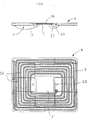
- FIG. 1 showing schematically and in plan a contactless card 1 of the type of those actually sold.
- an antenna 2 in the form of a large coil, slightly smaller than the size of the card, is integrated in the card body 3, and two ends of the antenna coil 2 are connected to power supply contacts 4,5 of an electronic module 6 carrying an integrated microcircuit 7 also called a chip.
- the coil is shown to scale, except for the number of turns, only four turns having been shown.
- Such an antenna makes it possible to read the information on the card, from a distance of 70 mm, for a frequency used of a few MHz.
- the general principle underlying the invention consists in eliminating the large antennas currently used for contactless cards, in order to eliminate the drawbacks mentioned above.
- the invention also seeks to use, in order to achieve the objectives of reliability and low manufacturing cost targeted, certain principles and the production lines used during the manufacture of contact cards, this manufacture now being well controlled and making it possible to obtain low manufacturing costs.
- the proposed solution is represented schematically on the card 1 in FIG. 2. It consists in using a particular smart card module 6 combining on the same small support, the electronic functions of the conventional smart modules, and the function transmit / receive antenna for contactless transmission of information between the card and an external read / write device (not shown).
- the module 6 has dimensions compatible with known production methods and used to manufacture contact cards, both in the thickness direction and in plan, in the length and width direction of the module.
- the antenna is obtained with dimensions compatible with those of the module, while retaining a number of turns ensuring the possibility of electromagnetic transmission at a sufficient distance, of the order of a few centimeters.
- the antenna is produced in the form of a spiral formed by a set of turns located directly on the support substrate and substantially in the same plane, which excludes the air coils taught by certain documents of the 'state of the art cited above.
- the antenna may have an outer coil of substantially square, rectangular, circular or oval shape, or any other suitable shape.
- the two ends of the antenna are connected to supply terminals of an integrated circuit, in particular a memory and / or a microprocessor, also located on the module, as shown diagrammatically at 7 in FIG. 2, but shown in more detail in FIGS. 4 to 6.
- FIG. 3 illustrating the separation of an electronic module 6 according to the invention, from a strip 8 comprising a plurality of modules 6 arranged for example in two rows.
- the manufacture of conventional electronic modules on such strips is well known in itself in the field of manufacturing contact cards, and will therefore not be described further.
- a module 6 according to the invention for example of the type comprising an integrated circuit 7 "straddling" on the turns of an antenna 2 in the form of a square spiral, is detached from the strip 8 by a cutting process, for example a mechanical cutting.
- the cut module is removed by automatic means not shown but known, and brought, preferably upside down (integrated circuit and antenna facing the bottom of the opening of the card body) in front of a blind opening 9 arranged in the card body 3 of a contactless smart card 1.
- the module 6 is fixed in the opening 9 provided by gluing, welding, or any other suitable means.
- FIGS. 4A to 4G show in more detail several variants of modules intended to be inserted for making contactless cards, or else integrated in a support of a shape different from the card, for example for making electronic labels.
- a module 6 is composed of a traditional support substrate 10 (in relatively flexible film, in mylar, epoxy or capton) on which is carried, not a coil, but an antenna pattern 2, which can be produced by several manners, as explained below.
- the antenna 2 is for example produced by stamping from a copper sheet, followed by assembly of the stamped sheet with the support substrate.
- the support substrate 10 and the antenna 2 are optionally assembled in a precise manner, using the known drive and positioning means of the substrate.
- the antenna 2 can also be obtained by photochemical etching of the antenna pattern, or by deposition of metallic material on a flexible film forming the substrate 10.
- the choice of the appropriate support substrate 10 has consequences on the thickness of the module, and mainly depends on the intended use for the module. This choice is entirely within the reach of the skilled person.
- the antenna 2 is constituted by a copper track of the order of 15 ⁇ m to 70 ⁇ m thick, produced in a spiral, with a distance between turns of the same size.
- the ends 11, 12 of this spiral are preferably widened so as to constitute contact pads for connection with the microcircuit 7.
- FIG. 4A a first practical and space-saving embodiment of the module 6 (FIG. 4A)
- the chip 7 is glued to the center of the antenna 2.
- FIG. 4B there are also shown connecting conductive wires 13, 14 for connecting a respective terminal of the chip 7 at a respective respective end 11, 12 of the antenna. To do this, it is necessary to pass a wire 15 above the tracks of the antenna.
- an insulator 16 is at previously deposited, in particular by screen printing, between the corresponding zone of the tracks, and the connecting wire 15.
- the antenna 2 occupies an entire side of the module and has no free space at its center.
- the invention provides for bonding the microcircuit 7 either on the face of the module devoid of antenna, or on the same face as the antenna (FIG. 4D), after interposition of an insulator (dark part 16) between antenna 2 and microcircuit 7.
- FIG. 4E is shown a variant of electronic module 6, in which the antenna 2 has the shape of a circular spiral, the microcircuit 7 being positioned above the plane of the turns, with the interposition of an insulator 16. This configuration minimizes the length of the connection wires between the antenna and the microcircuit.
- FIG. 4F is shown an additional variant of the module 6 according to the invention, particularly suitable in cases where an oblong or rectangular module is necessary.
- the antenna pattern 2 has a substantially oblong spiral shape
- the microcircuit 7 is preferably positioned in the center of the antenna, and connections between the terminals of the microcircuit and the pads of the coil are made as described. in conjunction with Figure 4B.
- connection between the studs of the chip and the contact terminals of the antenna can be carried out using a conventional technique of connection of conductive wires, such as for example the so-called bonding bond consisting of wires. conductors soldered between a stud of the microcircuit and a respective terminal of the antenna, or even using the so-called “flip-chip” technique consisting in transferring the microcircuit onto the module substrate 10, having the face carrying the antenna and the glued microcircuit on the substrate. The resin protection of the contacts is then carried out using the traditional methods of producing smart cards with contacts.
- FIG. 4G represents a more detailed view of an electronic module 6 according to the invention, on which a tuning capacitor 17 has been produced straddling the antenna turns, by depositing above an insulating layer 16 (grayed out part).
- a terminal 18 of the capacitor 17 is connected to the terminal 12 and to the stud 14, and the other terminal 19 of the capacitor 17 is connected to the terminal 11 and to the pad 13, by means of intermediate pads 20,21 connected by an intermediate connection 22 located between the intermediate pads 20,21 and produced above the insulating layer 16, so as not to short-circuit the turns of the antenna.
- tuning capacitor 17 Of course, other arrangements of the tuning capacitor 17 are possible. In particular, it will be possible to integrate it on the microcircuit 7 itself, at the design stage thereof, which will save module 6 manufacturing steps.
- the antenna pattern is determined to allow high frequency operation, of the order of Mhz, the value of the tuning capacitor 17 being chosen to obtain a determined operating frequency of the antenna 2 located in a range of high frequencies of the order of 1 MHz to 450 MHz.
- the tuning capacitor 17 has a value of the order of 12 to 180 picoFarad.
- the capacitor agrees to a value of the order of 30 to 500 picoFarad.
- Figures 5 and 6 show various embodiments of module 6, shown in section.
- a metal grid was used as the antenna, then cut and then glued onto a support substrate 10.
- the mechanical cutting of a spiral antenna is suitable for not too fine track widths, of the order of at least 300 ⁇ m at the current time.
- the microcircuit 7 and the antenna 2 are located on the two opposite faces of the support substrate 10 of the module, the contact terminals 11, 12 of the antenna 2 being connected to the pads of the microcircuit (not shown) by means of connection wires 15 brought through wells 23 made in the support 10.
- the microcircuit 7 is on the same side as the antenna 2, and arranged above its turns with the interposition of an insulator 16.
- the microcircuit 7 is placed in a cavity 25 provided for this purpose in the support 10 of the module, which makes it possible to reduce the thickness of the whole of the module 6.
- the microcircuit 7 is simply glued to the center of the antenna 2, as also shown in FIGS. 4A, 4B. In all cases, the antenna is entirely located on the support substrate 10 forming part of the module, and the microcircuit is attached to this substrate and antenna structure.
- the antenna 2 it is possible to use for the antenna 2 a grid engraved in or deposited by metallization or otherwise on a suitable support substrate 10, instead of a grid metal cut.
- FIG. 6 in which has been shown in section and in top view another embodiment of the electronic module 6, in order to obtain a contactless and contactless hybrid module, particularly suitable for the manufacture of hybrid cards.
- the microcircuit 7 and the antenna are arranged on a first face of the support substrate 10 of the module, as already described in connection with FIG. 5.
- usual contacts 26 identical to the contacts of contact cards are connected to corresponding pads of the microcircuit by conductive wires 27.
- the microcircuit will dialogue with the outside using the contacts 26 or the antenna 2, depending on the applied external signal. All the components useful for the operation of the hybrid card, including the antenna 2, are therefore placed on a hybrid module 6 of small dimensions, capable of being inserted, that is to say incorporated into a body of menu.
- two modules 6 of one of the types described above can be produced side by side in the width of a standard film 10 (i.e. 35 mm), but other arrangements of the modules 6 on a support strip 8 are included in the context of the invention.
- Each module 6 can then be transferred to a card body 3 in standard ISO format using the traditional method of transferring modules into the card bodies, as used for manufacturing contact cards.
- the modules 6 can be used for the manufacture of electronic labels, of the type used for the identification of objects. If necessary, after their cutting from the support strip 8, the modules 6 will be protected by a protective coating of resin or any other suitable material, which will make it possible to obtain labels of small dimensions at low cost.
- the modules can also be integrated into or fixed on different or larger supports (keys, packaging, etc.), depending on the intended application.
- FIG. 7 As an interesting variant of the method of manufacturing labels, in order to take advantage of economies of scale and lines for manufacturing contactless cards while using modules 6 according to the invention, it is also possible to manufacture electronic labels according to a method comprising only the step consisting in cutting an electronic module 6 as described above, from of a contactless card 1 incorporating such a module, so as to leave a little material around the card body around the electronic module 6, for the purpose of protecting the module 6. Thus, it is very easily obtained from contactless cards according to the invention, produced in large numbers, electronic labels having the thickness of a card, but of much smaller plan dimensions.
- This label 30 incorporates a module 6 protected on both sides, and is capable of being graphically personalized on both sides to make them labels usable in games or any other application.
- the dimensions of the module used are of the order of 12 mm x 12 mm, but we can envisage slightly larger oblong formats to increase performance, or even an optimization of the antenna of the reader or of the chip itself with regard to its consumption, to improve performance and achieve that of a larger antenna.
- the module 6 is used to manufacture cards, the integrity of the card body is preserved throughout the manufacturing process.
- the card body can therefore easily be used in the traditional way to receive a magnetic strip.
- it can be printed by any existing process without particular constraints, other than those known for the manufacture of a conventional contact card.
- the choice of material for the card body is completely free: it will therefore make it possible to adapt to the needs required by the various applications envisaged.
- the invention makes it possible to solve all of the aforementioned drawbacks related to the manufacture of contactless modules for contactless cards, and in particular that of cost, size, printing, compatibility with embossing or making a magnetic strip.
- the small dimensions of the antenna induce comparable advantages in the case of the manufacture of electronic labels which are not dependent on the shape of a card body.
- the economic interest of the invention is indisputable: it makes it possible to produce, on the same production lines, electronic modules with integrated antenna, electronic labels and functional contactless cards, at a fraction of the current cost observed in the processes used for the production of contactless cards or labels, and this at all stages of production.
Abstract
Description
La présente invention concerne le domaine des objets portatifs tels que notamment les étiquettes électroniques et les cartes à puce sans contact, pourvues d'un module électronique comprenant un microcircuit intégré.The present invention relates to the field of portable objects such as in particular electronic labels and contactless smart cards, provided with an electronic module comprising an integrated microcircuit.
L'invention concerne aussi un procédé de fabrication de tels modules et de tels objets portables.The invention also relates to a method of manufacturing such modules and such portable objects.
On connaît déjà des objets portables sous la forme de cartes sans contact, au format ISO, qui sont destinées à la réalisation de diverses opérations, telles que par exemple, des transactions de paiement de prestations de transport, téléphoniques ou autres. Ces opérations s'effectuent grâce à un couplage à distance entre le module électronique de la carte et un appareil récepteur ou lecteur. Le couplage peut être réalisé en mode lecture seule ou en mode lecture/écriture.Portable objects are already known in the form of contactless cards, in ISO format, which are intended for carrying out various operations, such as for example, payment transactions for transport, telephone or other services. These operations are carried out thanks to a remote coupling between the electronic module of the card and a receiver or reader device. The coupling can be carried out in read-only mode or in read / write mode.
En ce qui concerne les cartes, il est à noter que l'invention ne concerne pas uniquement les cartes ayant un fonctionnement exclusivement sans contact. Elle concerne également des cartes mixtes ou hybrides, qui ont la possibilité de fonctionner selon les deux modes: sans contact et par contact. Ces cartes mixtes sont destinées, par exemple, à des opérations du type télébilletique, dans lesquelles, après avoir été chargées en unités de valeur (unités monétaires, unités de paiement de prestations diverses), elle sont débitées à distance d'un certain nombre de ces unités de valeur lorsqu'elles passent au voisinage d'une borne de lecture: ce type de débit suppose un fonctionnement sans contact. Si nécessaire, ces cartes sont rechargées dans un distributeur adapté à cet effet.With regard to the cards, it should be noted that the invention does not only concern cards having exclusively contactless operation. It also relates to mixed or hybrid cards, which have the possibility of operating in two modes: contactless and contactless. These mixed cards are intended, for example, for telephone-type transactions, in which, after having been loaded in value units (monetary units, payment units for various services), they are debited remotely from a certain number of these value units when they pass in the vicinity of a reading terminal: this type of flow requires contactless operation. If necessary, these cards are recharged in a dispenser suitable for this purpose.
Pour les besoins de la présente description, et à titre de simplification, on désignera aussi bien les cartes mixtes que les cartes sans contact, par la même terminologie de cartes sans contact.For the purposes of this description, and by way of simplification, both mixed cards and contactless cards will be designated by the same terminology of contactless cards.
On connaît par ailleurs des objets portables sous la forme d'étiquettes électroniques, généralement utilisées pour diverses opérations d'identification ou de suivi. Elles sont composées d'une part d'un module électronique à microcircuit, et d'autre part d'un support de ce module associé à une antenne bobinée fonctionnant à fréquence relativement basse (150 Khz) et de dimensions relativement grandes par rapport à celles du module.Portable objects are also known in the form of electronic labels, generally used for various identification or tracking operations. They are composed on the one hand of an electronic microcircuit module, and on the other hand of a support of this module associated with a wound antenna operating at relatively low frequency (150 Khz) and of relatively large dimensions compared to those of the module.
Telles qu'ils sont réalisés actuellement, les objets portables en forme d'étiquettes électroniques comportent des antennes ayant un grand nombre de tours, souvent supérieur à 100, et leurs dimensions rendent leur manipulation délicate, notamment au cours des étapes de fabrication des étiquettes mettant en oeuvre la connexion par soudure de l'antenne au microcircuit du module.As they are currently produced, portable objects in the form of electronic labels include antennas having a large number of turns, often greater than 100, and their dimensions make them difficult to handle, especially during the steps of manufacturing labels putting implement the connection by welding of the antenna to the microcircuit of the module.
De façon similaire, les objets portables en forme de cartes sans contact présentent également des inconvénients. Telles qu'elles sont réalisées actuellement, les cartes sans contact sont des objets portables de dimensions normalisées. Une norme usuelle mais nullement limitative pour la présente invention est celle dite ISO 7810 qui correspond à une carte de format standard de 85 mm de longueur, de 54 mm de largeur, et de 0,76 mm d'épaisseur.Similarly, portable objects in the form of contactless cards also have drawbacks. As they are currently produced, contactless cards are portable objects of standardized dimensions. A standard which is customary but in no way limiting for the present invention is that known as ISO 7810 which corresponds to a standard format card 85 mm in length, 54 mm in width, and 0.76 mm in thickness.
Dans la plupart des cartes sans contact connues, chaque carte comporte un corps de carte réalisé par un assemblage de feuilles en matière plastique, et noyé dans cet assemblage, un module électronique comprenant un circuit intégré ou microcircuit encore appelé « puce », relié à l'aide de deux bornes de connexion, à une antenne bobinée du type self inductance. La puce comporte une mémoire, et peut dans certains cas comporter un microprocesseur. Les dimensions du module électronique sont sensiblement inférieures aux dimensions de la carte, le module étant en général positionné dans l'un des coins de la carte, puisque les contraintes mécaniques imposées au module du fait des flexions de la carte y sont moins élevées qu'au centre de la carte.In most of the known contactless cards, each card comprises a card body produced by an assembly of plastic sheets, and embedded in this assembly, an electronic module comprising an integrated circuit or microcircuit also called a "chip", connected to the using two connection terminals, to a wound inductance type antenna. The chip includes a memory, and can in some cases include a microprocessor. The dimensions of electronic module are significantly smaller than the dimensions of the card, the module being generally positioned in one of the corners of the card, since the mechanical stresses imposed on the module due to the bending of the card are lower there than in the center of the map.
Dans certaines cartes sans contact connues cependant, un corps de carte pourvu d'une cavité est prévu, et un module pourvu d'une bobine connectée à un circuit intégré est prévu, pour assurer un fonctionnement sans contact de la carte.In certain known contactless cards, however, a card body provided with a cavity is provided, and a module provided with a coil connected to an integrated circuit is provided, to ensure contactless operation of the card.
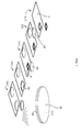
Dans cette catégorie de cartes sans contact, on connait en particulier, d'après le DE-A-43 11 493 (AMATECH), une unité d'assemblage pour la fabrication d'unités d'identification au format carte.In this category of contactless cards, we know in particular, according to DE-A-43 11 493 (AMATECH), an assembly unit for the manufacture of identification units in card format.
Selon un premier mode de réalisation, un module 21 comporte un support de module 28 sur lequel est fixée une puce de circuit intégré 29. Une bobine 30 surmonte la puce 29, de façon à donner au module une capacité d'identification sans contact. Ce document précise que la distance de lecture entre le module et le lecteur sans contact est faible. En outre, aucune carte à puce utilisant un tel module avec antenne n'a apparemment encore été commercialisée, compte tenu des problèmes de coût et de faible portée qui se posent nécessairement avec la structure de module décrite.According to a first embodiment, a
En outre, il est à noter que dans ce document, l'antenne se présente sous la forme d'une antenne à air bobinée, rapportée au-dessus de la puce, ce qui présente des difficultés de réalisation, de coût, de rendement, et de manque d'homogénéité des performances.In addition, it should be noted that in this document, the antenna is in the form of a coil air antenna, attached above the chip, which presents difficulties in terms of construction, cost, efficiency, and inconsistent performance.
On connait également, d'après le DE 37 21 822 C1 (PHILIPS), une carte à puce à fonctionnement sans contact, dont la conception est destinée à résoudre un problème de mauvaise connexion entre la bobine et le circuit intégré. A cet effet, ce document décrit une carte à puce sans module, une antenne 4 étant réalisée à même le semiconducteur sur lequel est réalisé le circuit intégré 5. En effet, l'antenne est réalisée en même temps que les pistes supérieures du circuit intégré, de sorte qu'il en résulte un circuit intégré de 4 x 6 à 6 x 8 mm2, portant 20 petites spires.According to DE 37 21 822 C1 (PHILIPS), there is also known a contactless chip card, the design of which is intended to solve a problem of poor connection between the coil and the integrated circuit. To this end, this document describes a chip card without module, an
Il en résulte que la surface utile de l'antenne est très faible, ce qui nuit à la portée. En outre, la carte selon ce document ne peut pas être fabriquée de façon très économique. En effet, on sait que la taille d'une pastille semiconductrice élémentaire est un des principaux facteurs de coût d'un circuit intégré produit en grandes quantités. Or dans ce document, la taille minimale du circuit intégré incorporant l'antenne est de l'ordre de 24 mm2 au minimum, alors que les cartes sans contact bon marché utilisent en général des microcircuits dont la taille est très petite, de l'ordre de 1 mm2.As a result, the useful surface area of the antenna is very small, which affects the range. In addition, the card according to this document cannot be produced very economically. Indeed, it is known that the size of an elementary semiconductor chip is one of the main cost factors of an integrated circuit produced in large quantities. However, in this document, the minimum size of the integrated circuit incorporating the antenna is of the order of at least 24 mm 2 , while inexpensive contactless cards generally use microcircuits whose size is very small, from order of 1 mm 2 .
On connaît encore une pluralité d'autres procédés de réalisation de cartes sans contact, tels que ceux décrits dans les demandes de brevet français de la même demanderesse, déposées sous les numéros 95 400305.9, 95 400365.3, et 95 400790.2. Ces demandes de brevet ont en commun de décrire une carte sans contact pourvue d'une antenne sensiblement de la taille de la carte, connectée à un micromodule portant la puce.A plurality of other methods of making contactless cards are also known, such as those described in the French patent applications of the same applicant, filed under the numbers 95 400305.9, 95 400365.3, and 95 400790.2. These patent applications have in common the description of a contactless card provided with an antenna substantially the size of the card, connected to a micromodule carrying the chip.
Une telle antenne présente l'avantage d'une portée relativement élevée pour un champ magnétique de lecture ou d'écriture donné. En effet, la relation qui lie la force électromotrice E apparaissant aux bornes de l'antenne de réception lorsqu'elle coupe un champ électromagnétique est du type suivant:![]()
![]()
Or, afin de faire fonctionner les circuits de la puce de la carte pour initialiser et effectuer une opération de lecture, la tension Er doit dépasser un certain seuil, qui est en général de l'ordre de 3 Volts.However, in order to operate the circuits of the card chip to initialize and perform a read operation, the voltage E r must exceed a certain threshold, which is generally of the order of 3 Volts.
On voit donc que pour une distance de lecture ou d'écriture D donnée que l'on cherche à atteindre avec la carte sans contact, il faut augmenter la surface de la spire moyenne et/ou le nombre N de spires de l'antenne, du côté lecture et/ou écriture.It can therefore be seen that for a given reading or writing distance D that one seeks to achieve with the contactless card, it is necessary to increase the surface of the mean turn and / or the number N of turns of the antenna, on the reading and / or writing side.
L'efficacité de l'antenne sera conditionnée, à la fréquence retenue pour la lecture ou l'écriture, par le coefficient de surtension de la bobine d'antenne, qui est donné par l'expression:![]()
![]()
Les grandeurs L et R ayant des influences contraires sur l'efficacité de l'antenne, elles ont tendance à se compenser, de sorte que le véritable facteur d'efficacité de l'antenne est surtout lié à la surface totale S.N de l'antenne.The quantities L and R having opposite influences on the efficiency of the antenna, they tend to compensate each other, so that the real factor of efficiency of the antenna is mainly related to the total surface SN of the antenna .
Or pour une dimension de bobine planaire donnée, le nombre N de spires est limité par la largeur d'une spire et par l'intervalle entre deux spires, qui dépendent de la technologie de réalisation.However, for a given planar coil dimension, the number N of turns is limited by the width of a turn and by the interval between two turns, which depend on the technology of production.
On voit donc que, toutes choses étant égales par ailleurs, la tendance naturelle pour obtenir une bonne antenne pour carte sans contact, et qui a été largement utilisée dans la pratique, consiste à utiliser sur la carte sans contact une antenne dont la taille de chaque spire se rapproche autant que possible de la surface de la carte. C'est pourquoi les cartes sans contact commercialisées comportent une antenne intégrée dans le corps de carte, au voisinage de la périphérie de celui-ci.We therefore see that, all other things being equal, the natural tendency to obtain a good antenna for contactless cards, and which has been widely used in practice, consists in using on the contactless card an antenna whose size of each turn turns as close as possible to the surface of the card. This is why contactless cards sold have an antenna integrated in the card body, in the vicinity of the periphery thereof.
Mais, comme l'expérience de la fabrication de telles cartes sans contact l'a montré, ce choix entraîne également un certain nombre d'inconvénients.However, as experience in the manufacture of such contactless cards has shown, this choice also involves a certain number of drawbacks.
En effet, la manipulation d'une antenne de cette taille en vue de son intégration dans la carte et de son raccordement électrique au module électronique pose de sérieux problèmes techniques (comme d'ailleurs dans le cas précité des étiquettes électroniques).Indeed, the manipulation of an antenna of this size with a view to its integration into the card and its electrical connection to the electronic module poses serious technical problems (as indeed in the aforementioned case of electronic labels).
En effet, malgré les techniques utilisées, l'assemblage de la carte et de l'antenne reste souvent complexe et coûteux, puisqu'il faut raccorder le module électronique et la bobine d'antenne avec des moyens difficiles à automatiser. Ensuite, l'assemblage subit une lamination, qui est un procédé coûteux nécessitant l'adjonction de résine pour pouvoir noyer la bobine et le module dans la carte de telle manière qu'ils n'apparaissent pas à la surface de la carte et ne déforment pas les feuilles supérieures et inférieures utilisées pour la colamination.Indeed, despite the techniques used, the assembly of the card and the antenna often remains complex and expensive, since it is necessary to connect the electronic module and the antenna coil with means that are difficult to automate. Then, the assembly undergoes a lamination, which is an expensive process requiring the addition of resin to be able to drown the coil and the module in the card in such a way that they do not appear on the surface of the card and do not deform not the upper and lower sheets used for colamination.
En outre, la complexité du procédé ne permet pas l'obtention de rendements comparables à ceux obtenus lors de la fabrication des cartes à contact. Ceci est d'autant plus vrai lorsqu'on intègre les contraintes requises par certains types d'impression de la carte, et par la présence éventuelle d'une piste magnétique ou d'un embossage. En effet, pour certains types d'impression de la carte, ou pour la réalisation d'une bande magnétique sur la carte, celle-ci doit présenter une planéité quasi-parfaite, avec des défauts inférieurs à 6 µm. En cas d'embossage, il faut choisir des matériaux compatibles avec le procédé de fabrication de la carte, et l'antenne doit notamment laisser libre la zone prévue pour l'embossage, faute de quoi elle serait abîmée lors de l'embossage.In addition, the complexity of the process does not allow yields comparable to those obtained during the manufacture of contact cards to be obtained. This is all the more true when the constraints required by certain types of printing of the card are integrated, and by the possible presence of a magnetic strip or an embossing. Indeed, for certain types of printing of the card, or for the production of a magnetic strip on the card, the latter must have an almost perfect flatness, with defects of less than 6 μm. In case of embossing, materials compatible with the card manufacturing process must be chosen, and the antenna must notably leave free the area provided for embossing, otherwise it would be damaged during embossing.
Compte tenu de l'ensemble des inconvénients liés aux modes actuels de fabrication de cartes sans contact et d'étiquettes électroniques, qui se traduisent principalement par un coût de fabrication élevé, les ingénieurs de la demanderesse se sont donnés pour objectif de proposer des procédés nouveaux de fabrication de cartes et d 'étiquettes sans contact, susceptibles d'éviter l'ensemble des inconvénients cités.Given all of the drawbacks associated with current methods of manufacturing contactless cards and electronic labels, which mainly result in a high manufacturing cost, the engineers of the applicant have set themselves the objective of proposing new methods for manufacturing contactless cards and labels, capable of avoiding all of the drawbacks mentioned.
Plus précisément, le but de la présente invention est de proposer des moyens peu coûteux aptes à être utilisés lors de la fabrication d'objets portables du type cartes à puce et/ou d'étiquettes électroniques.More specifically, the aim of the present invention is to propose inexpensive means suitable for being used during the manufacture of portable objects of the smart card and / or electronic label type.
Un autre but de l'invention est de fournir des procédés de fabrication de cartes et d'étiquettes sans contact, de faible coût, permettant une fabrication fiable et de qualité à l'aide de machines automatisées.Another object of the invention is to provide methods of manufacturing contactless cards and labels, of low cost, allowing reliable and quality manufacturing using automated machines.
Un autre but de l'invention est de proposer un procédé de fabrication permettant d'obtenir des cartes sans contact parfaitement planes.Another object of the invention is to propose a manufacturing method making it possible to obtain perfectly flat contactless cards.
Un but supplémentaire de l'invention est de proposer un procédé de fabrication de cartes sans contact, qui soit compatible avec toutes les étapes subséquentes à l'assemblage du corps de carte et de l'antenne, et notamment avec l'impression offset des cartes, l'embossage de la carte, ou le dépôt d'une piste magnétique.A further object of the invention is to propose a method of manufacturing contactless cards, which is compatible with all the steps subsequent to the assembly of the card body and the antenna, and in particular with offset printing of cards. , embossing the card, or filing a magnetic stripe.
A cet effet, l'invention propose un objet portable électronique comportant un support recevant une antenne connectée à un microcircuit électronique, caractérisée en ce que l'antenne est formée d'un motif d'antenne disposé directement sur le support et sensiblement dans un même plan.To this end, the invention provides an electronic portable object comprising a support receiving an antenna connected to an electronic microcircuit, characterized in that the antenna is formed by an antenna pattern placed directly on the support and substantially in the same plan.
Selon d'autres caractéristiques avantageuses de l'invention:
- le motif d'antenne forme une spirale comportant plusieurs spires;
- l'antenne est constituée par une spirale de dimensions extérieures de l'ordre de 5 à 15 mm, de préférence de l'ordre de 12 mm, dont les bornes;d'extrémités sont reliées à des plots de contact du microcircuit électronique;
- l'antenne est constituée par une spirale conductrice comportant entre environ 6 et environ 50 spires, chaque spire possèdant une largeur de l'ordre de 50 à 300 µm, l'espacement entre deux spires contiguës étant de l'ordre de 50 à 200 µm;
- l'objet comprend un fil de
liaison 15 pour relier une extrémité de l'antenne à une borne du microcircuit électronique, ledit fil traversant des spires d'antenne, unisolant 16 étant déposé au préalable entre une zone correspondant aux spires traversées et le fil de liaison; - l'antenne est obtenue par dépôt de matière métallique sur le support.
- l'isolant est déposé par sérigraphie;
- le microcircuit est monté en flip chip;
- le microcircuit est disposé dans une fenêtre du support;
- la plus grande dimension du support est de l'ordre de 5 à 15 mm,
- le microcircuit est disposé au centre de l'antenne et du même coté du module que l'antenne, les bornes de connexion de l'antenne étant reliées à des plots de contact correspondants respectifs du module ou du microcircuit par l'intermédiaire de fils conducteurs;
- le microcircuit électronique est disposé du côté du support dépourvu d'antenne, et des fils conducteurs traversant des puits aménagés dans le substrat de support du module au niveau desdites bornes de connexion de l'antenne;
- l'objet comprend un condensateur d'accord dont la valeur est choisie pour obtenir une fréquence de fonctionnement du module située dans une plage de l'ordre de 1 Mhz à 450 Mhz.
- le condensateur d'accord a une valeur de l'ordre de 12 à 180 picoFarad, et en ce que la fréquence de fonctionnement du
module est d'environ 13,56 Mhz.; - le condensateur d'accord a une valeur de l'ordre de 30 à 500 picoFarad, et en ce que la fréquence de fonctionnement du
module est d'environ - le condensateur d'accord est obtenu par dépôt de silicium oxydé sur la surface du microcircuit, préalablement revêtu d'un isolant;
- l'objet comporte sur une face du support une antenne connectée au microcircuit, et sur l'autre face du support, des contacts apparents et également connectés au microcircuit, de façon à obtenir une carte hybride pouvant être lue et écrite par l'intermédiaire des contacts et/ou de l'antenne.
- le module électronique pourvu de son microcircuit et de son antenne est fixé sur ou intégré à un support, de sorte que l'étiquette peut être rendue solidaire d'un objet à identifier.
- the antenna pattern forms a spiral comprising several turns;
- the antenna is formed by a spiral with external dimensions of the order of 5 to 15 mm, preferably of the order of 12 mm, the terminals of which are connected at the contact pads of the electronic microcircuit;
- the antenna is constituted by a conductive spiral comprising between approximately 6 and approximately 50 turns, each turn having a width of the order of 50 to 300 μm, the spacing between two contiguous turns being of the order of 50 to 200 μm ;
- the object comprises a connecting
wire 15 for connecting one end of the antenna to a terminal of the electronic microcircuit, said wire passing through antenna turns, aninsulator 16 being deposited beforehand between an area corresponding to the turns crossed and the wire link; - the antenna is obtained by depositing metallic material on the support.
- the insulation is deposited by screen printing;
- the microcircuit is mounted as a flip chip;
- the microcircuit is placed in a window of the support;
- the largest dimension of the support is of the order of 5 to 15 mm,
- the microcircuit is placed in the center of the antenna and on the same side of the module as the antenna, the antenna connection terminals being connected to respective corresponding contact pads of the module or of the microcircuit via conductive wires ;
- the electronic microcircuit is arranged on the side of the support without antenna, and conductive wires passing through wells arranged in the support substrate of the module at said antenna connection terminals;
- the object comprises a tuning capacitor whose value is chosen to obtain an operating frequency of the module situated in a range of the order of 1 Mhz to 450 Mhz.
- the tuning capacitor has a value of the order of 12 to 180 picoFarad, and in that the operating frequency of the module is approximately 13.56 Mhz .;
- the tuning capacitor has a value of the order of 30 to 500 picoFarad, and in that the operating frequency of the module is approximately 8.2 MHz.
- the tuning capacitor is obtained by depositing oxidized silicon on the surface of the microcircuit, previously coated with an insulator;
- the object comprises on one face of the support an antenna connected to the microcircuit, and on the other face of the support, visible contacts and also connected to the microcircuit, so as to obtain a hybrid card which can be read and written via the contacts and / or antenna.
- the electronic module provided with its microcircuit and its antenna is fixed on or integrated into a support, so that the label can be made integral with an object to be identified.
L'invention a également pour objet un procédé de fabrication d'un objet portable électronique. Il se distingue en ce qu'il comporte des étapes consistant à:
- réaliser par dépôt de matière métallique sur un support (10) une antenne spirale plane, pourvue de bornes de connexion;
- fixer sur ledit support ou ladite antenne, un microcircuit pourvu de plots de contact;
- réaliser la connexion électrique entre des bornes de connexion de l'antenne et des plots de contact correspondants du microcircuit.
- producing a metallic spiral antenna, provided with connection terminals, by depositing metallic material on a support (10);
- fix on said support or said antenna, a microcircuit provided with contact pads;
- make the electrical connection between the antenna connection terminals and the corresponding contact pads of the microcircuit.
L'invention sera mieux comprise en se référant à la description suivante faite à titre d'exemple non limitatif et aux dessins ci-annexés, dans lesquels:
- la figure 1 représente une carte sans contact selon l'état de la technique;
- la figure 2 représente une carte sans contact selon l'invention;
- la figure 3 représente une bande utilisée pour la fabrication en continu de modules électroniques selon l'invention, destinés à des cartes sans contact ou à des étiquettes électroniques selon l'invention, ainsi qu'une carte destinée à recevoir le module;
- les figures 4A à 4G représentent plusieurs variantes de réalisation d'un module électronique selon l'invention, apte ou destiné à être incorporé dans le corps d'une carte sans contact ou dans une étiquette électronique;
- les figures 5A à 5D représentent en vue en coupe plusieurs variantes de réalisation d'un module électronique pourvu d'une antenne, selon l'invention;
- la figure 6 représente en coupe un module pour carte hybride à contact et sans contact.
- la figure 7 représente les étapes d'un procédé de fabrication d'une variante d'étiquette électronique utilisant le module électronique selon l'invention.
- FIG. 1 represents a contactless card according to the state of the art;
- FIG. 2 represents a contactless card according to the invention;
- FIG. 3 represents a strip used for the continuous manufacture of electronic modules according to the invention, intended for contactless cards or electronic labels according to the invention, as well as a card intended to receive the module;
- FIGS. 4A to 4G represent several alternative embodiments of an electronic module according to the invention, suitable or intended to be incorporated in the body of a contactless card or in an electronic label;
- FIGS. 5A to 5D show in section view several alternative embodiments of an electronic module provided with an antenna, according to the invention;
- FIG. 6 represents in section a module for a contact and contactless hybrid card.
- FIG. 7 represents the steps of a method of manufacturing a variant of electronic label using the electronic module according to the invention.
Des éléments similaires sont désignés par les mêmes numéros de référence dans l'ensemble des figures.Similar elements are designated by the same reference numbers in all of the figures.
On se réfère à la figure 1 montrant de façon schématique et en plan une carte sans contact 1 du type de celles effectivement commercialisées. Comme on le voit, une antenne 2 sous la forme d'une bobine de grande dimension, légèrement inférieure à la dimension de la carte, est intégrée dans le corps de carte 3, et deux extrémités de la bobine d'antenne 2 sont connectées à des contacts d'alimentation 4,5 d'un module électronique 6 portant un microcircuit intégré 7 encore appelé une puce.Reference is made to FIG. 1 showing schematically and in plan a
La bobine est représentée à l'échelle, sauf en ce qui concerne le nombre de spires, seules quatre spires ayant été représentées. Pour assembler une telle bobine 2 avec le corps de carte 3, il est nécessaire d'effectuer des opérations de laminage ou d'injection complexes et coûteuses, avec les inconvénients mentionnés précédemment. Une telle antenne permet de lire les informations de la carte, à partir d'une distance de 70 mm, pour une fréquence utilisée de quelques Mhz.The coil is shown to scale, except for the number of turns, only four turns having been shown. To assemble such a
A la différence de la carte de la figure 1, le principe général sous-jacent à l'invention consiste à éliminer les antennes de grande taille actuellement utilisées pour les cartes sans contact, afin de supprimer les inconvénients mentionnés plus haut. L'invention cherche également à utiliser, pour atteindre les objectifs de fiabilité et de faible coût de fabrication visés, certains principes et les chaînes de fabrication utilisés lors de la fabrication de cartes à contact, cette fabrication étant maintenant bien maîtrisée et permettant d'obtenir des coûts de fabrication faibles.Unlike the card in FIG. 1, the general principle underlying the invention consists in eliminating the large antennas currently used for contactless cards, in order to eliminate the drawbacks mentioned above. The invention also seeks to use, in order to achieve the objectives of reliability and low manufacturing cost targeted, certain principles and the production lines used during the manufacture of contact cards, this manufacture now being well controlled and making it possible to obtain low manufacturing costs.
La solution proposée est représentée de façon schématique sur la carte 1 de la figure 2. Elle consiste à utiliser un module particulier 6 de carte à puce combinant sur un même support de faibles dimensions, les fonctions électroniques des modules classiques à puce, et la fonction d'antenne d'émission/réception pour la transmission sans contact d'informations entre la carte et un dispositif de lecture/écriture extérieur (non représenté).The proposed solution is represented schematically on the
Le module 6 présente des dimensions compatibles avec les procédés de réalisation connus et utilisés pour fabriquer les cartes à contact, à la fois dans le sens de l'épaisseur et en plan, dans le sens de la longueur et de la largeur du module.The
Bien entendu, pour qu'un module pourvu d'une antenne soit réalisable, il faut que, à l'inverse des enseignements de l'état de la technique, l'antenne soit obtenue avec des dimensions compatibles avec celles du module, tout en conservant un nombre de spires assurant la possibilité d'une transmission électromagnétique à une distance suffisante, de l'ordre de quelques centimètres. A cet effet, l'antenne est réalisée sous la forme d'une spirale formée d'un ensemble de spires situées directement sur le substrat de support et sensiblement dans le même plan, ce qui exclut les bobines à air enseignées par certains documents de l'état de la technique cité plus haut.Of course, for a module provided with an antenna to be feasible, it is necessary that, contrary to the teachings of the state of the art, the antenna is obtained with dimensions compatible with those of the module, while retaining a number of turns ensuring the possibility of electromagnetic transmission at a sufficient distance, of the order of a few centimeters. For this purpose, the antenna is produced in the form of a spiral formed by a set of turns located directly on the support substrate and substantially in the same plane, which excludes the air coils taught by certain documents of the 'state of the art cited above.
Afin de s'adapter au mieux à la forme du module et à la surface disponible, l'antenne peut avoir une spire extérieure de forme sensiblement carrée, rectangulaire, circulaire ou ovale, ou toute autre forme appropriée. Les deux extrémités de l'antenne sont connectées à des bornes d'alimentation d'un circuit intégré, notamment une mémoire et/ou un microprocesseur, situé(e) également sur le module, comme schématisé en 7 sur la figure 2, mais représenté plus en détail dans les figures 4 à 6.In order to best adapt to the shape of the module and the available surface, the antenna may have an outer coil of substantially square, rectangular, circular or oval shape, or any other suitable shape. The two ends of the antenna are connected to supply terminals of an integrated circuit, in particular a memory and / or a microprocessor, also located on the module, as shown diagrammatically at 7 in FIG. 2, but shown in more detail in FIGS. 4 to 6.
On se réfère à la figure 3 illustrant la séparation d'un module électronique 6 selon l'invention, à partir d'une bande 8 comportant une pluralité de modules 6 disposés par exemple selon deux rangées. La fabrication de modules électroniques classiques sur de telles bandes est bien connue en elle-même dans le domaine de la fabrication de cartes à contact, et ne sera de ce fait pas décrite davantage.Referring to Figure 3 illustrating the separation of an
Un module 6 selon l'invention, par exemple du type comportant un circuit intégré 7 « à cheval » sur les spires d'une antenne 2 en forme de spirale carrée, est détaché de la bande 8 par un procédé de découpe, par exemple une découpe mécanique. Le module découpé est prélevé par des moyens automatiques non représentés mais connus, et amené, de préférence à l'envers (circuit intégré et antenne tournés vers le fond de l'ouverture du corps de carte) en face d'une ouverture borgne 9 aménagée dans le corps de carte 3 d'une carte à puce 1 sans contact. La fixation du module 6 dans l'ouverture 9 prévue est faite par collage, soudure, ou tout autre moyen approprié.A
Il en résulte une carte sans contact conforme à l'invention, pourvue d'une antenne 2 localisée au niveau du module électronique 6, et dont la fabrication se réduit principalement aux étapes qui viennent d'êtres décrites, suivies bien entendu le cas échéant d'étapes d'impression et de personnalisation classiques.This results in a contactless card according to the invention, provided with an
Les figures 4A à 4G représentent de manière plus détaillée plusieurs variantes de modules destinés à être encartés pour fabriquer des cartes sans contact, ou encore intégrés dans un support de forme différente de la carte, par exemple pour fabriquer des étiquettes électroniques.FIGS. 4A to 4G show in more detail several variants of modules intended to be inserted for making contactless cards, or else integrated in a support of a shape different from the card, for example for making electronic labels.
Un module 6 est composé d'un substrat de support 10 traditionnel (en film relativement flexible, en mylar, epoxy ou capton ) sur lequel est reporté, non pas une bobine, mais un motif d'antenne 2, qui peut être réalisé de plusieurs manières, comme expliqué plus loin. L'antenne 2 est par exemple réalisée par emboutissage à partir d'une feuille en cuivre, suivi d'un assemblage de la feuille emboutie avec le substrat de support. Le substrat de support 10 et l'antenne 2 sont le cas échéant assemblés de manière précise, en utilisant les moyens d'entraînement et de positionnement connus du substrat.A
L'antenne 2 peut aussi être obtenue par gravure photochimique du motif d'antenne, ou par dépôt de matière métallique sur un film flexible formant le substrat 10. Le choix du substrat de support 10 approprié a des conséquences sur l'épaisseur du module, et dépend principalement de l'utilisation visée pour le module. Ce choix est entièrement à la portée de l'homme de métier.The
Dans une variante proposée pour le module électronique 6, l'antenne 2 est constituée par une piste de cuivre de l'ordre de 15 µm à 70 µm d'épaisseur, réalisée en spirale, avec une distance entre spires de même grandeur. Les extrémités 11,12 de cette spirale sont de préférence élargies de façon à constituer des plots de contact pour la liaison avec le microcircuit 7.In a variant proposed for the
Plusieurs variantes de positionnement respectif du microcircuit et de l'antenne sont prévus. Dans un premier mode de réalisation pratique et peu encombrant du module 6 (figure 4A), la puce 7 est collée au centre de l'antenne 2. En figure 4B, on a également représenté des fils conducteurs de liaison 13,14 pour relier une borne respective de la puce 7 à une extrémité respective correspondante 11,12 de l'antenne. Pour ce faire, il est nécessaire de passer un fil 15 au-dessus des pistes de l'antenne. A cet effet, un isolant 16 est au préalable déposé, notamment par sérigraphie, entre la zone correspondante des pistes, et le fil de liaison 15.Several variants of respective positioning of the microcircuit and the antenna are provided. In a first practical and space-saving embodiment of the module 6 (FIG. 4A), the
Dans un autre mode de réalisation du module 6 (figure 4C), l'antenne 2 occupe tout un côté du module et est dépourvue d'espace libre en son centre. Dans ce cas, l'invention prévoit de coller le microcircuit 7 soit sur la face du module dépourvue d'antenne, soit sur la même face que l'antenne (figure 4D), après interposition d'un isolant (partie sombre 16) entre l'antenne 2 et le microcircuit 7.In another embodiment of the module 6 (FIG. 4C), the
En figure 4E est représentée une variante de module électronique 6, dans laquelle l'antenne 2 a la forme d'une spirale circulaire, le microcircuit 7 étant positionné au-dessus du plan des spires, avec interposition d'un isolant 16. Cette configuration permet de minimiser la longueur des fils de connexion entre l'antenne et le microcircuit.In FIG. 4E is shown a variant of
En figure 4F est représentée une variante supplémentaire du module 6 selon l'invention, particulièrement adaptée dans les cas où un module oblong ou rectangulaire est nécessaire. Dans ce cas, le motif d'antenne 2 a une forme de spirale sensiblement oblongue, le microcircuit 7 est de préférence positionné au centre de l'antenne, et des connexions entre les bornes du microcircuit et les plots de la bobine sont réalisés comme décrit en liaison avec la figure 4B.In FIG. 4F is shown an additional variant of the
Il est à noter que la connexion entre les plots de la puce et les bornes de contact de l'antenne peut être réalisée en utilisant une technique conventionnelle de connexion de fils conducteurs, comme par exemple la liaison dite par « bonding » consistant en des fils conducteurs soudés entre un plot du microcircuit et une borne respective de l'antenne, ou encore en utilisant la technique dite de « flip-chip » consistant à reporter le microcircuit sur le substrat de module 10, en ayant la face portant l'antenne et le microcircuit collée sur le substrat. La protection par résine des contacts est ensuite effectuée en utilisant les procédés traditionnels de réalisation des cartes à puce à contacts.It should be noted that the connection between the studs of the chip and the contact terminals of the antenna can be carried out using a conventional technique of connection of conductive wires, such as for example the so-called bonding bond consisting of wires. conductors soldered between a stud of the microcircuit and a respective terminal of the antenna, or even using the so-called “flip-chip” technique consisting in transferring the microcircuit onto the
La figure 4G représente en vue plus détaillée un module électronique 6 selon l'invention, sur lequel un condensateur d'accord 17 a été réalisé à cheval sur les spires d'antenne, par dépôt au-dessus d'une couche d'isolant 16 (partie grisée). Afin de connecter le condensateur en parallèle entre les bornes 11,12 de l'antenne 2 et les plots 13,14 du microcircuit, une borne 18 du condensateur 17 est reliée à la borne 12 et au plot 14, et l'autre borne 19 du condensateur 17 est reliée à la borne 11 et au plot 13, par l'intermédiaire de plots intermédiaires 20,21 reliés par une connexion intermédiaire 22 située entre les plots intermédiaires 20,21 et réalisée au-dessus de la couche isolante 16, de façon à ne pas court-circuiter les spires de l'antenne.FIG. 4G represents a more detailed view of an
Bien entendu, d'autres dispositions du condensateur d'accord 17 sont possibles. Il sera en particulier possible de l'intégrer sur le microcircuit 7 lui-même, au stade de conception de celui-ci, ce qui économisera des étapes de fabrication du module 6.Of course, other arrangements of the tuning
Le motif d'antenne est déterminé pour permettre un fonctionnement à haute fréquence, de l'ordre du Mhz, la valeur du condensateur d'accord 17 étant choisie pour obtenir une fréquence déterminée de fonctionnement de l'antenne 2 située dans une plage de hautes fréquences de l'ordre de 1 Mhz à 450 Mhz. Dans un exemple de réalisation permettant d'obtenir une fréquence de fonctionnement usuelle d'environ 13,56 Mhz, le condensateur d'accord 17 a une valeur de l'ordre de 12 à 180 picoFarad. Dans une autre variante permettant un fonctionnement à 8,2 Mhz, le condensateur d'accord à une valeur de l'ordre de 30 à 500 picoFarad.The antenna pattern is determined to allow high frequency operation, of the order of Mhz, the value of the tuning
Les figures 5 et 6 montrent divers modes de réalisation du module 6, représenté en coupe. En figure 5, on a utilisé comme antenne une grille métallique découpée puis collée sur un substrat de support 10. Le découpage mécanique d'une antenne spiralée convient pour des largeurs de pistes pas trop fines, de l'ordre de 300 µm au minimum à l'heure actuelle.Figures 5 and 6 show various embodiments of
En figure 5A, le microcircuit 7 et l'antenne 2 sont situés sur les deux faces opposées du substrat de support 10 du module, les bornes de contact 11,12 de l'antenne 2 étant connectés à des plots du microcircuit (non représentés) par l'intermédiaire de fils de connexion 15 amenés à travers des puits 23 réalisés dans le support 10.In FIG. 5A, the
En figure 5B, le microcircuit 7 est du même côté que l'antenne 2, et disposé au-dessus de ses spires avec interposition d'un isolant 16. En figure 5C, le microcircuit 7 est disposé dans une cavité 25 aménagée à cet effet dans le support 10 du module, ce qui permet de diminuer l'épaisseur de l'ensemble du module 6. En figure 5D, le microcircuit 7 est simplement collé au centre de l'antenne 2, comme montré également en figures 4A,4B. Dans tous les cas, l'antenne est entièrement située sur le substrat de support 10 faisant partie du module, et le microcircuit est rapporté sur cette structure de substrat et d'antenne.In FIG. 5B, the
Il est à noter que pour réduire encore l'épaisseur du module 6, il est possible d'utiliser pour l'antenne 2 une grille gravée dans ou déposée par métallisation ou autrement sur un substrat de support 10 approprié, au lieu d'une grille métallique découpée.It should be noted that to further reduce the thickness of the
On se réfère maintenant à la figure 6, dans laquelle a été représentée en coupe et en vue de dessus une autre forme de réalisation du module électronique 6, afin d'obtenir un module hybride à contact et sans contact, particulièrement adapté à la fabrication de cartes hybrides. Dans ce module, le microcircuit 7 et l'antenne sont disposés sur une première face du substrat de support 10 du module, comme déjà décrit en liaison avec la figure 5. En outre, des contacts 26 usuels identiques aux contacts des cartes à contact sont connectés à des plots correspondants du microcircuit par des fils conducteurs 27. Le microcircuit dialoguera avec l'extérieur en utilisant les contacts 26 ou l'antenne 2, en fonction du signal extérieur appliqué. L'ensemble des composants utiles pour le fonctionnement de la carte hybride, y compris l'antenne 2, est donc disposé sur un module hybride 6 de faibles dimensions, apte à être encarté, c'est-à-dire incorporé dans un corps de carte.Referring now to Figure 6, in which has been shown in section and in top view another embodiment of the
De façon avantageuse, deux modules 6 de l'un des types décrits plus haut pourront être réalisés côte à côte dans la largeur d'un film 10 standard (soit 35 mm), mais d'autres arrangements des modules 6 sur une bande de support 8 sont compris dans le cadre de l'invention. Chaque module 6 pourra être ensuite reporté sur un corps de carte 3 au format ISO standard en utilisant le procédé traditionnel de report des modules dans les corps de cartes, tel qu'utilisé pour la fabrication de cartes à contacts.Advantageously, two
Alternativement, les modules 6 peuvent être utilisés pour la fabrication d'étiquettes électroniques, du type de celles utilisées pour l'identification d'objets. Si nécessaire, après leur découpe à partir de la bande de support 8, les modules 6 seront protégés par un revêtement protecteur en résine ou tout autre matériau approprié, ce qui permettra d'obtenir à faible coût des étiquettes de petites dimensions. Bien entendu, les modules peuvent également être intégrés à ou fixés sur des supports différents ou plus volumineux (clés, emballages, etc...), en fonction de l'application visée.Alternatively, the
On se réfère à la figure 7. En variante intéressante du procédé de fabrication d'étiquettes, afin de profiter des économies d'échelle et des lignes de fabrication de cartes sans contact tout en utilisant des modules 6 selon l'invention, il est également possible de fabriquer des étiquettes électroniques selon un procédé comprenant uniquement l'étape consistant à découper un module électronique 6 tel que décrit plus haut, à partir d'une carte sans contact 1 incorporant un tel module, de façon à laisser subsister autour du module électronique 6 un peu de matière du corps de carte, à des fins de protection du module 6. Ainsi, on obtient à très facilemnt à partir de cartes sans contact selon l'invention, fabriquées en grand nombre, des étiquettes électroniques présentant l'épaisseur d'une carte, mais de dimensions en plan beaucoup plus faibles.Reference is made to FIG. 7. As an interesting variant of the method of manufacturing labels, in order to take advantage of economies of scale and lines for manufacturing contactless cards while using
Il apparait cependant dans ce cas un inconvénient qui peut être majeur dans certaines applications: en procédant par simple découpage à partir d'une carte sans contact, l'étiquette n'est protégée d'un côté que par la protection très minime procurée sur un côté de la cavité de la carte par un voile de matière plastique d'une centaine de micromètres d'épaisseur, alors que l'autre face du module est exposée. Pour remédier à cet inconvénient, il est possible de manière judicieuse de découper dans une partie de la carte 1 représentée en Figure 7(a), qui serait de toute manière jetée, une première pièce 28 au format prévu pour l'étiquette. Puis comme représenté dans la figure 7(b), on reporte cette pièce 28 sur la face de l'étiquette montrant le module 6 apparent et non protégé. L pièce 28 est assemblée sur la carte 1 comme représnté en figure 7(d), par une technique quelconque appropriée, notamment le collage ou la soudure par ultrasons. Enfin, comme représenté en figure 7(e), on découpe à nouveau dans la carte une pièce 29 au format de la pièce 28 et au niveau de celle-ci. On obtient ainsi pour un coût minimal, une étiquette électronique 30 symétrique représentée agrandie en figure 7(f). Bien entendu, on pourrait aussi découper les pièces 28, 29 séparément pour les assembler par la suite.There appears however in this case a drawback which can be major in certain applications: by proceeding by simple cutting from a contactless card, the label is protected on one side only by the very minimal protection provided on a side of the card cavity by a plastic veil of a hundred micrometers thick, while the other face of the module is exposed. To remedy this drawback, it is judiciously possible to cut from a part of the
Cette étiquette 30 incorpore un module 6 protégé des deux côtés, et est susceptible d'être personalisée graphiquement des deux côtés pour en faire des étiquettes utilisables dans des jeux ou toutes autres applications.This
En ce qui concerne les performances des modules, cartes et étiquettes selon l'invention, les résultats théoriques et pratiques montrent que l'on obtient sur le module 6 une antenne performante pouvant fonctionner dans la gamme de fréquences de 1 à 450 Mhz.With regard to the performance of the modules, cards and labels according to the invention, the theoretical and practical results show that an efficient antenna can be obtained on the
Pour obtenir les performances de liaison recherchées pour une application donnée, il suffit d'utiliser une fréquence de modulation suffisamment élevée (13,56 Mhz par exemple) pour obtenir des performances acceptables en distance de lecture/écriture.To obtain the desired link performance for a given application, it suffices to use a sufficiently high modulation frequency (13.56 Mhz for example) to obtain acceptable performance in read / write distance.
Si l'on considère par exemple la fréquence de 13,56 Mhz couramment utilisée dans les applications télébilletiques, les performances obtenues sont tout à fait remarquables. Une puce 7 montée par ce procédé permet d'obtenir actuellement avec l'antenne 2 associée, une distance de fonctionnement de l'ordre de 50 mm là où la même puce montée avec une bobine classique aux dimensions d'une carte permet d'atteindre environ 70 à 75 mm. Cette différence n'est pas critique dans la plupart des applications sans contact visées à l'heure actuelle. De plus, ces performances pourront être sensiblement améliorées en travaillant au niveau des circuits d'émission et de récupération d'énergie électromagnétique du module et des lecteurs externes.If we consider for example the frequency of 13.56 Mhz commonly used in teleticketing applications, the performances obtained are quite remarkable. A
Selon un exemple de réalisation pratique, les dimensions du module utilisé sont de l'ordre de 12 mm x 12 mm, mais on peut envisager des formats oblongs légèrement plus grands pour augmenter les performances, ou encore une optimisation de l'antenne du lecteur ou de la puce elle-même en ce qui concerne sa consommation, pour améliorer les performances et atteindre celles d'une antenne de plus grande taille.According to a practical embodiment, the dimensions of the module used are of the order of 12 mm x 12 mm, but we can envisage slightly larger oblong formats to increase performance, or even an optimization of the antenna of the reader or of the chip itself with regard to its consumption, to improve performance and achieve that of a larger antenna.
Grâce au concept de l'invention, en cas d'utilisation du module 6 pour fabriquer des cartes, l'intégrité du corps de carte est conservée pendant tout le processus de fabrication. Le corps de carte peut donc aisément être utilisé de manière traditionnelle pour recevoir une piste magnétique. De plus, il pourra être imprimé par tous les procédés existants sans contraintes particulières, autres que celles connues pour la fabrication d'une carte à contact classique. De même, le choix du matériau du corps de carte est tout à fait libre: il permettra donc de s'adapter aux besoins requis par les diverses applications envisagées.Thanks to the concept of the invention, if the
En conséquence, l'invention permet de résoudre d'un trait tous les inconvénients précités liés à la fabrication de modules sans contact pour cartes sans contact, et notamment celui du coût, de l'encombrement, de l'impression, de la compatibilité avec l'embossage ou la réalisation d'une piste magnétique. Les faibles dimensions de l'antenne induisent des avantages comparables en cas de fabrication d'étiquettes électroniques qui ne sont pas tributaires de la forme d'un corps de carte.Consequently, the invention makes it possible to solve all of the aforementioned drawbacks related to the manufacture of contactless modules for contactless cards, and in particular that of cost, size, printing, compatibility with embossing or making a magnetic strip. The small dimensions of the antenna induce comparable advantages in the case of the manufacture of electronic labels which are not dependent on the shape of a card body.
L'intérêt économique de l'invention est incontestable: elle permet de réaliser sur les mêmes chaînes de fabrication, des modules électroniques à antenne intégrée, des étiquettes électroniques et des cartes sans contact fonctionnelles, à une fraction du coût actuel constaté dans les procédés utilisés pour la production de cartes ou d'étiquettes sans contact, et ceci à toutes les étapes de fabrication.The economic interest of the invention is indisputable: it makes it possible to produce, on the same production lines, electronic modules with integrated antenna, electronic labels and functional contactless cards, at a fraction of the current cost observed in the processes used for the production of contactless cards or labels, and this at all stages of production.
D'autres avantages annexes liés au module, à l'étiquette électronique et à la carte sans contact selon l'invention et à leurs procédés de fabrication résident dans le fait qu'il n'y a pas de manipulation de bobine d'antenne, ni de soudure à l'étain, de positionnement précis de la bobine, ou d'impression avant encartage.Other additional advantages linked to the module, the electronic label and the contactless card according to the invention and to their manufacturing processes reside in the fact that there is no handling of antenna coil, tin soldering, precise positioning of the coil, or printing before inserting.
Claims (19)
Applications Claiming Priority (4)
| Application Number | Priority Date | Filing Date | Title |
|---|---|---|---|
| FR9600889 | 1996-01-17 | ||
| FR9600889A FR2743649B1 (en) | 1996-01-17 | 1996-01-17 | CONTACTLESS ELECTRONIC MODULE, ELECTRONIC LABEL CARD INCORPORATING THE SAME, AND METHODS OF MAKING SAME |
| EP01103498A EP1118960B1 (en) | 1996-01-17 | 1997-01-17 | Contactless electronic module for a card or a label |
| EP97901116A EP0875039B1 (en) | 1996-01-17 | 1997-01-17 | Contactless electronic module for a card or label |
Related Parent Applications (3)
| Application Number | Title | Priority Date | Filing Date |
|---|---|---|---|
| EP01103498A Division EP1118960B1 (en) | 1996-01-17 | 1997-01-17 | Contactless electronic module for a card or a label |
| EP97901116.0 Division | 1997-07-24 | ||
| EP01103498.0 Division | 2001-02-15 |
Publications (2)
| Publication Number | Publication Date |
|---|---|
| EP1492048A2 true EP1492048A2 (en) | 2004-12-29 |
| EP1492048A3 EP1492048A3 (en) | 2005-12-14 |
Family
ID=9488485
Family Applications (3)
| Application Number | Title | Priority Date | Filing Date |
|---|---|---|---|
| EP97901116A Expired - Lifetime EP0875039B1 (en) | 1996-01-17 | 1997-01-17 | Contactless electronic module for a card or label |
| EP01103498A Expired - Lifetime EP1118960B1 (en) | 1996-01-17 | 1997-01-17 | Contactless electronic module for a card or a label |
| EP04019527A Withdrawn EP1492048A3 (en) | 1996-01-17 | 1997-01-17 | Portable contactless electronic device and its manufacturing process |
Family Applications Before (2)
| Application Number | Title | Priority Date | Filing Date |
|---|---|---|---|
| EP97901116A Expired - Lifetime EP0875039B1 (en) | 1996-01-17 | 1997-01-17 | Contactless electronic module for a card or label |
| EP01103498A Expired - Lifetime EP1118960B1 (en) | 1996-01-17 | 1997-01-17 | Contactless electronic module for a card or a label |
Country Status (14)
| Country | Link |
|---|---|
| US (2) | US20020089049A1 (en) |
| EP (3) | EP0875039B1 (en) |
| JP (2) | JP3779328B2 (en) |
| KR (1) | KR19990077335A (en) |
| CN (1) | CN1165873C (en) |
| AT (2) | ATE274214T1 (en) |
| AU (1) | AU713433B2 (en) |
| BR (1) | BR9709153A (en) |
| CA (1) | CA2243326C (en) |
| DE (2) | DE69706280T2 (en) |
| ES (2) | ES2226994T3 (en) |
| FR (1) | FR2743649B1 (en) |
| RU (1) | RU2194306C2 (en) |
| WO (1) | WO1997026621A1 (en) |
Cited By (2)
| Publication number | Priority date | Publication date | Assignee | Title |
|---|---|---|---|---|
| US7605453B2 (en) | 2005-08-11 | 2009-10-20 | Infineon Technologies Ag | Chip module and chip card |
| US8305213B2 (en) | 2004-01-23 | 2012-11-06 | Semiconductor Energy Laboratory Co., Ltd. | Film-like article and method for manufacturing the same |
Families Citing this family (102)
| Publication number | Priority date | Publication date | Assignee | Title |
|---|---|---|---|---|
| JPH10203066A (en) * | 1997-01-28 | 1998-08-04 | Hitachi Ltd | Non-contact ic card |
| FR2765010B1 (en) * | 1997-06-20 | 1999-07-16 | Inside Technologies | ELECTRONIC MICROMODULE, ESPECIALLY FOR CHIP CARDS |
| DE19732644C1 (en) * | 1997-07-29 | 1998-11-12 | Siemens Ag | Production of non-contact smart cards with printed information |
| US5909050A (en) * | 1997-09-15 | 1999-06-01 | Microchip Technology Incorporated | Combination inductive coil and integrated circuit semiconductor chip in a single lead frame package and method therefor |
| FR2769390B1 (en) * | 1997-10-08 | 2003-02-14 | Gemplus Card Int | METHOD FOR MANUFACTURING CHIP CARDS SUITABLE FOR PROVIDING CONTACT AND NON-CONTACT OPERATION, AND CONTACTLESS CHIP CARDS |
| WO1999026195A1 (en) * | 1997-11-14 | 1999-05-27 | Toppan Printing Co., Ltd. | Composite ic module and composite ic card |
| IL122250A (en) | 1997-11-19 | 2003-07-31 | On Track Innovations Ltd | Smart card amenable to assembly using two manufacturing stages and a method of manufacture thereof |
| JP2001515661A (en) * | 1998-01-09 | 2001-09-18 | マイクロチップ テクノロジー インコーポレイテッド | Integrated circuit (IC) package including accompanying IC chip and coil and method of manufacturing the same |
| EP0977145A3 (en) * | 1998-07-28 | 2002-11-06 | Kabushiki Kaisha Toshiba | Radio IC card |
| JP3180086B2 (en) * | 1998-08-31 | 2001-06-25 | 株式会社シーメディア | Mobile communication device, information transmission system and method, non-contact IC media usable in mobile communication device |
| US6630370B2 (en) | 1998-10-02 | 2003-10-07 | Shinko Electric Industries Co., Ltd. | Process for manufacturing IC card |
| TW484101B (en) * | 1998-12-17 | 2002-04-21 | Hitachi Ltd | Semiconductor device and its manufacturing method |
| WO2000038109A1 (en) * | 1998-12-18 | 2000-06-29 | Koninklijke Philips Electronics N.V. | Data carrier module with integrated circuit and transmission coil |
| FR2787609B1 (en) * | 1998-12-21 | 2001-02-09 | Gemplus Card Int | NON-CONTACT CHIP CARD MANUFACTURING PROCESS |
| DE59900131D1 (en) † | 1999-01-23 | 2001-07-26 | Ident Gmbh X | RFID transponder with printable surface |
| EP1031940A1 (en) * | 1999-02-24 | 2000-08-30 | Sihl GmbH | Device comprising a plurality of electronic circuits |
| FR2794264B1 (en) * | 1999-05-27 | 2001-11-02 | Gemplus Card Int | ADAPTER FOR PORTABLE ELECTRONIC DEVICE WITH INTEGRATED CIRCUIT, OF THE CHIP CARD TYPE, OF A REDUCED FORMAT IN RELATION TO THE STANDARD FORMAT OF A MINI-CARD |
| JP3928682B2 (en) * | 1999-06-22 | 2007-06-13 | オムロン株式会社 | Wiring board bonded body, wiring board bonding method, data carrier manufacturing method, and electronic component module mounting apparatus |
| FR2796208B1 (en) * | 1999-07-08 | 2002-10-25 | Gemplus Card Int | ANTENNA FOR CONTACTLESS CHIP CARD, HYBRID CARDS AND ELECTRONIC LABELS |
| FR2796760B1 (en) * | 1999-07-23 | 2002-02-01 | Gemplus Card Int | ELECTRONIC LABEL AND METHOD FOR ITS MANUFACTURE |
| JP2001256456A (en) * | 2000-03-10 | 2001-09-21 | Shinko Electric Ind Co Ltd | Ic tag and its manufacture |
| US20020099473A1 (en) * | 2000-11-08 | 2002-07-25 | Paul Amadeo | Integrated computer-aided design (CAD) and robotic systems for rapid prototyping and manufacture of smart cards |
| FR2820548A1 (en) * | 2001-02-02 | 2002-08-09 | Schlumberger Systems & Service | PORTABLE CHIP AND ANTENNA OBJECT, MODULE FOR FORMING PORTABLE CHIP AND ANTENNA OBJECT AND METHODS OF MAKING SAME |
| KR100746742B1 (en) * | 2001-02-03 | 2007-08-06 | 삼성전자주식회사 | Reader coil antenna and non-contacting type card identification system using the same |
| JP4684433B2 (en) * | 2001-02-07 | 2011-05-18 | 大日本印刷株式会社 | Contact / non-contact IC module and manufacturing method thereof |
| DE10120269C1 (en) * | 2001-04-25 | 2002-07-25 | Muehlbauer Ag | Microchip transponder manufacturing method has chip module carrier band combined with antenna carrier band with chip module terminals coupled to antenna |
| KR20010099429A (en) * | 2001-09-27 | 2001-11-09 | 김경현 | System of Checking falsification of an identification card |
| US6774470B2 (en) | 2001-12-28 | 2004-08-10 | Dai Nippon Printing Co., Ltd. | Non-contact data carrier and method of fabricating the same |
| JP4109039B2 (en) * | 2002-08-28 | 2008-06-25 | 株式会社ルネサステクノロジ | Inlet for electronic tag and manufacturing method thereof |
| JP4141857B2 (en) * | 2003-02-18 | 2008-08-27 | 日立マクセル株式会社 | Semiconductor device |
| EP1623367A1 (en) * | 2003-05-05 | 2006-02-08 | Axalto SA | Method for making a pre-laminated inlet |
| US7243421B2 (en) * | 2003-10-29 | 2007-07-17 | Conductive Inkjet Technology Limited | Electrical connection of components |
| US7612677B2 (en) | 2005-01-28 | 2009-11-03 | Smartrac Ip B.V. | Method for producing a security layered construction and security layered construction and identification documents containing such a construction |
| US7196397B2 (en) * | 2004-03-04 | 2007-03-27 | International Rectifier Corporation | Termination design with multiple spiral trench rings |
| DE102004011702B4 (en) | 2004-03-10 | 2006-02-16 | Circle Smart Card Ag | Method for producing a card body for a contactless chip card |
| EP1738303B1 (en) * | 2004-03-25 | 2008-09-17 | Bauer, Eric | Method for making an electronic label |
| US7825447B2 (en) * | 2004-04-28 | 2010-11-02 | Semiconductor Energy Laboratory Co., Ltd. | MOS capacitor and semiconductor device |
| US7798415B1 (en) | 2004-05-20 | 2010-09-21 | American Express Travel Realted Services Company, Inc. | Wireless transaction fobs and methods of using the same |
| US7604176B2 (en) * | 2004-05-20 | 2009-10-20 | American Express Travel Related Services Company, Inc. | Radio frequency fobs and methods of using the same |
| FR2882174B1 (en) * | 2005-02-11 | 2007-09-07 | Smart Packaging Solutions Sps | METHOD FOR MANUFACTURING A MICROELECTRONIC DEVICE WITH NON-CONTACT FUNCTIONING, IN PARTICULAR FOR ELECTRONIC PASSPORT |
| JP2006271596A (en) * | 2005-03-29 | 2006-10-12 | Aruze Corp | Game card |
| CN100361150C (en) * | 2005-06-24 | 2008-01-09 | 清华大学 | Radio frequency identification marking card with silicon base integrated antenna |
| FR2890212B1 (en) | 2005-08-30 | 2009-08-21 | Smart Packaging Solutions Sps | ELECTRONIC MODULE WITH A DOUBLE COMMUNICATION INTERFACE, IN PARTICULAR FOR A CHIP CARD |
| JP4997779B2 (en) * | 2006-02-13 | 2012-08-08 | 大日本印刷株式会社 | Contactless data carrier |
| EP1863090A1 (en) * | 2006-06-01 | 2007-12-05 | Semiconductor Energy Laboratory Co., Ltd. | Semiconductor device and method for manufacturing semiconductor device |
| KR100809028B1 (en) * | 2006-06-07 | 2008-03-03 | (주)아이디밸리 | A passcard rf module |
| FR2904723B1 (en) * | 2006-08-01 | 2008-12-19 | Arjowiggins Security Soc Par A | SECURITY STRUCTURE, IN PARTICULAR FOR A DOCUMENT OF SECURITY AND / OR VALUE |
| JP2008246104A (en) * | 2007-03-30 | 2008-10-16 | Angel Shoji Kk | Game card incorporating rfid and its manufacturing method |
| FR2937448B1 (en) * | 2008-10-17 | 2012-11-16 | Oberthur Technologies | MODULE, MICROCIRCUIT CARD AND CORRESPONDING MANUFACTURING METHOD. |
| US8188926B2 (en) * | 2008-10-31 | 2012-05-29 | Silicon Laboratories, Inc. | Folded antenna structures for portable devices |
| US8186603B2 (en) * | 2009-09-22 | 2012-05-29 | On Track Innovation Ltd. | Contactless smart sticker |
| SE534533C2 (en) | 2009-10-07 | 2011-09-27 | Pampett Ab | Method and system for detecting moisture in an absorbent article |
| FR2963142B1 (en) * | 2010-07-20 | 2012-09-14 | Oberthur Technologies | NON-CONTACT TYPE MICROCIRCUIT CARD |
| US9112272B2 (en) | 2010-08-12 | 2015-08-18 | Feinics Amatech Teoranta | Antenna modules for dual interface smart cards, booster antenna configurations, and methods |
| US9195932B2 (en) | 2010-08-12 | 2015-11-24 | Féinics Amatech Teoranta | Booster antenna configurations and methods |
| US9033250B2 (en) | 2010-08-12 | 2015-05-19 | Féinics Amatech Teoranta | Dual interface smart cards, and methods of manufacturing |
| US8789762B2 (en) | 2010-08-12 | 2014-07-29 | Feinics Amatech Teoranta | RFID antenna modules and methods of making |
| US9272370B2 (en) | 2010-08-12 | 2016-03-01 | Féinics Amatech Teoranta | Laser ablating structures for antenna modules for dual interface smartcards |
| US8991712B2 (en) | 2010-08-12 | 2015-03-31 | Féinics Amatech Teoranta | Coupling in and to RFID smart cards |
| DE102010036057A1 (en) * | 2010-09-01 | 2012-03-01 | Giesecke & Devrient Gmbh | Chip module with marking |
| EP2463809A1 (en) * | 2010-12-07 | 2012-06-13 | NagraID S.A. | Electronic card with electric contact including an electronic unit and/or an antenna |
| JP5344000B2 (en) * | 2011-05-09 | 2013-11-13 | 大日本印刷株式会社 | IC module and IC card for both contact and non-contact |
| US9634391B2 (en) | 2011-08-08 | 2017-04-25 | Féinics Amatech Teoranta | RFID transponder chip modules |
| US9489613B2 (en) | 2011-08-08 | 2016-11-08 | Féinics Amatech Teoranta | RFID transponder chip modules with a band of the antenna extending inward |
| US9812782B2 (en) | 2011-08-08 | 2017-11-07 | Féinics Amatech Teoranta | Coupling frames for RFID devices |
| US9622359B2 (en) | 2011-08-08 | 2017-04-11 | Féinics Amatech Teoranta | RFID transponder chip modules |
| DE102011056329A1 (en) * | 2011-12-13 | 2013-06-13 | Infineon Technologies Ag | Smart card module of smart card e.g. payment card, has chip external coil and chip external capacitor that are arranged to form a module arrangement which produces resonant frequency corresponding to operating frequency |
| EP2669852A1 (en) | 2012-05-31 | 2013-12-04 | Gemalto SA | Integrated circuit chip module with antenna |
| FR2992761B1 (en) * | 2012-07-02 | 2015-05-29 | Inside Secure | METHOD FOR MANUFACTURING CONTACTLESS MICROCIRCUIT |
| FR2994005B1 (en) * | 2012-07-25 | 2017-05-26 | Microconnections Sas | ELECTRONIC MODULE FOR A CHIP CARD AND PRINTED CIRCUIT FOR CARRYING OUT SUCH A MODULE |
| US9286564B2 (en) * | 2012-11-20 | 2016-03-15 | Xerox Corporation | Apparatuses and methods for printed radio frequency identification (RFID) tags |
| EP2736001A1 (en) * | 2012-11-27 | 2014-05-28 | Gemalto SA | Electronic module with three-dimensional communication interface |
| US10248902B1 (en) | 2017-11-06 | 2019-04-02 | Féinics Amatech Teoranta | Coupling frames for RFID devices |
| US11354560B2 (en) | 2013-01-18 | 2022-06-07 | Amatech Group Limited | Smartcards with multiple coupling frames |
| US11551051B2 (en) | 2013-01-18 | 2023-01-10 | Amatech Group Limiied | Coupling frames for smartcards with various module opening shapes |
| JP6124119B2 (en) * | 2013-03-29 | 2017-05-10 | パナソニックIpマネジメント株式会社 | Power feeding device and power receiving device |
| DE102013104567A1 (en) * | 2013-05-03 | 2014-11-06 | Infineon Technologies Ag | Chip arrangement, chip card arrangement and method for producing a chip arrangement |
| EP2892012A1 (en) | 2014-01-06 | 2015-07-08 | Gemalto SA | Electronic module, method for manufacturing same and electronic device including such a module |
| WO2015113184A1 (en) * | 2014-01-29 | 2015-08-06 | 北京嘉岳同乐极电子有限公司 | High sensitivity magnetic sensor and manufacturing method thereof |
| US10839282B2 (en) | 2014-03-08 | 2020-11-17 | Féinics Amatech Teoranta | RFID transponder chip modules, elements thereof, and methods |
| CN103984977A (en) * | 2014-05-27 | 2014-08-13 | 江苏远洋数据股份有限公司 | Double-interface card |
| US10438110B2 (en) | 2015-07-08 | 2019-10-08 | Assa Abloy Ab | Multiple frequency transponder with a single antenna |
| EP3182336A1 (en) | 2015-12-14 | 2017-06-21 | Gemalto Sa | Radiofrequency device with adjustable lc circuit including an electric and/or electronic module |
| EP3182507A1 (en) | 2015-12-15 | 2017-06-21 | Gemalto Sa | Single-sided antenna module with smd component |
| DE102016114199B4 (en) * | 2016-08-01 | 2021-07-22 | Infineon Technologies Ag | CHIP CARD MODULE, CHIP CARD, CHIP CARD ARRANGEMENT, METHOD FOR DESIGNING A CHIP CARD MODULE AND METHOD FOR DESIGNING A CHIP CARD |
| FR3058545B1 (en) * | 2016-11-04 | 2018-10-26 | Smart Packaging Solutions | METHOD FOR MANUFACTURING AN ELECTRONIC MODULE FOR A CHIP CARD |
| WO2019169003A1 (en) * | 2018-02-27 | 2019-09-06 | Thin Film Electronics Asa | Printed and/or thin film integrated circuit with integrated antenna, and methods of making and using the same |
| EP3663984A1 (en) | 2018-12-06 | 2020-06-10 | Thales Dis France SA | Method for manufacturing a smart card with interconnection of modules |
| EP3663983A1 (en) | 2018-12-06 | 2020-06-10 | Thales Dis France SA | Method for manufacturing a smart card, metal or not, with relay antenna |
| EP3671561A1 (en) | 2018-12-21 | 2020-06-24 | Thales Dis France SA | Method for manufacturing a metal radiofrequency smart card with improved electromagnetic permittivity |
| EP3671563A1 (en) | 2018-12-21 | 2020-06-24 | Thales Dis France SA | Method for manufacturing a metal smart card, preferably with relay antenna |
| EP3671564A1 (en) | 2018-12-21 | 2020-06-24 | Thales Dis France SA | Method for manufacturing an insert for radiofrequency smart card comprising a metal plate |
| EP3671562A1 (en) | 2018-12-21 | 2020-06-24 | Thales Dis France SA | Method for manufacturing a metal radiofrequency smart card with improved permittivity with extended perforations |
| JP1662551S (en) * | 2019-09-06 | 2020-06-29 | ||
| EP3789919A1 (en) | 2019-09-09 | 2021-03-10 | Thales Dis France SA | Method for manufacturing a metal smart card with relay mini antenna |
| EP3832547A1 (en) | 2019-12-02 | 2021-06-09 | Thales Dis France Sa | The invention concerns a method for manufacturing a radiofrequency chip card comprising a metal plate with a slot in the plate |
| EP3832546A1 (en) | 2019-12-02 | 2021-06-09 | Thales Dis France Sa | Method for manufacturing a radiofrequency chip card comprising a metal plate with a slot or a gap in the plate |
| USD943024S1 (en) | 2020-07-30 | 2022-02-08 | Federal Card Services, LLC | Asymmetrical arrangement of contact pads and connection bridges of a transponder chip module |
| USD942538S1 (en) | 2020-07-30 | 2022-02-01 | Federal Card Services, LLC | Asymmetrical arrangement of contact pads and connection bridges of a transponder chip module |
| US11551050B2 (en) * | 2020-11-12 | 2023-01-10 | Advanide Holdings Pte. Ltd. | Card inlay for direct connection or inductive coupling technology |
| EP4012612A1 (en) | 2020-12-11 | 2022-06-15 | Thales DIS France SA | Method for manufacturing a smart card with positioning of metal insert |
| CN112990416B (en) * | 2021-04-22 | 2021-11-19 | 四川谦泰仁投资管理有限公司 | High-frequency RFID chip and label with antenna detection port |
Citations (3)
| Publication number | Priority date | Publication date | Assignee | Title |
|---|---|---|---|---|
| US4857893A (en) * | 1986-07-18 | 1989-08-15 | Bi Inc. | Single chip transponder device |
| US5153583A (en) * | 1987-11-18 | 1992-10-06 | Uniscan Ltd. | Transponder |
| EP1331602A2 (en) * | 1994-02-14 | 2003-07-30 | Gemplus | Hybrid card with antenna and manufacturing equipment |
Family Cites Families (12)
| Publication number | Priority date | Publication date | Assignee | Title |
|---|---|---|---|---|
| AU1712188A (en) * | 1987-04-27 | 1988-12-02 | Soundcraft, Inc. | Method for manufacture of and structure of a laminated proximity card |
| DE3721822C1 (en) * | 1987-07-02 | 1988-11-10 | Philips Patentverwaltung | Chip card |
| FR2641102B1 (en) * | 1988-12-27 | 1991-02-22 | Ebauchesfabrik Eta Ag | |
| DE8909783U1 (en) * | 1989-08-16 | 1990-09-13 | Pepperl & Fuchs Gmbh, 6800 Mannheim, De | |
| JPH04152191A (en) * | 1990-10-17 | 1992-05-26 | Mitsubishi Electric Corp | Tab base and non-contact ic card using said tab base |
| FR2678753B1 (en) * | 1991-07-02 | 1996-12-20 | Gemplus Card Int | MANUFACTURE OF SELF-DETACHING CHIP CARDS. |
| DE4311493C2 (en) * | 1993-04-07 | 2000-04-06 | Amatech Advanced Micromechanic | IC card module for producing an IC card |
| ATE176345T1 (en) * | 1993-04-14 | 1999-02-15 | Ake Gustafson | ELECTRONIC MARKING DEVICE |
| JP3305843B2 (en) * | 1993-12-20 | 2002-07-24 | 株式会社東芝 | Semiconductor device |
| DE4403753C1 (en) * | 1994-02-08 | 1995-07-20 | Angewandte Digital Elektronik | Combined chip card |
| FR2787609B1 (en) * | 1998-12-21 | 2001-02-09 | Gemplus Card Int | NON-CONTACT CHIP CARD MANUFACTURING PROCESS |
| DE10016715C1 (en) * | 2000-04-04 | 2001-09-06 | Infineon Technologies Ag | Laminated smart card arrangement e.g. for telephone card |
-
1996
- 1996-01-17 FR FR9600889A patent/FR2743649B1/en not_active Expired - Lifetime
-
1997
- 1997-01-17 AT AT01103498T patent/ATE274214T1/en not_active IP Right Cessation
- 1997-01-17 DE DE69706280T patent/DE69706280T2/en not_active Expired - Lifetime
- 1997-01-17 AT AT97901116T patent/ATE204662T1/en not_active IP Right Cessation
- 1997-01-17 WO PCT/FR1997/000098 patent/WO1997026621A1/en not_active Application Discontinuation
- 1997-01-17 AU AU14477/97A patent/AU713433B2/en not_active Expired
- 1997-01-17 EP EP97901116A patent/EP0875039B1/en not_active Expired - Lifetime
- 1997-01-17 BR BR9709153A patent/BR9709153A/en not_active Application Discontinuation
- 1997-01-17 CN CNB971929130A patent/CN1165873C/en not_active Expired - Lifetime
- 1997-01-17 EP EP01103498A patent/EP1118960B1/en not_active Expired - Lifetime
- 1997-01-17 RU RU98115301/09A patent/RU2194306C2/en active
- 1997-01-17 JP JP52575497A patent/JP3779328B2/en not_active Expired - Lifetime
- 1997-01-17 ES ES01103498T patent/ES2226994T3/en not_active Expired - Lifetime
- 1997-01-17 CA CA002243326A patent/CA2243326C/en not_active Expired - Lifetime
- 1997-01-17 ES ES97901116T patent/ES2163114T3/en not_active Expired - Lifetime
- 1997-01-17 DE DE69730362T patent/DE69730362T2/en not_active Expired - Lifetime
- 1997-01-17 EP EP04019527A patent/EP1492048A3/en not_active Withdrawn
- 1997-01-17 KR KR1019980705482A patent/KR19990077335A/en active Search and Examination
- 1997-01-27 US US09/101,049 patent/US20020089049A1/en not_active Abandoned
- 1997-01-27 US US10/254,736 patent/US6794727B2/en not_active Expired - Lifetime
-
2001
- 2001-10-03 JP JP2001307817A patent/JP2002207987A/en active Pending
Patent Citations (3)
| Publication number | Priority date | Publication date | Assignee | Title |
|---|---|---|---|---|
| US4857893A (en) * | 1986-07-18 | 1989-08-15 | Bi Inc. | Single chip transponder device |
| US5153583A (en) * | 1987-11-18 | 1992-10-06 | Uniscan Ltd. | Transponder |
| EP1331602A2 (en) * | 1994-02-14 | 2003-07-30 | Gemplus | Hybrid card with antenna and manufacturing equipment |
Cited By (2)
| Publication number | Priority date | Publication date | Assignee | Title |
|---|---|---|---|---|
| US8305213B2 (en) | 2004-01-23 | 2012-11-06 | Semiconductor Energy Laboratory Co., Ltd. | Film-like article and method for manufacturing the same |
| US7605453B2 (en) | 2005-08-11 | 2009-10-20 | Infineon Technologies Ag | Chip module and chip card |
Also Published As
| Publication number | Publication date |
|---|---|
| AU713433B2 (en) | 1999-12-02 |
| EP1118960A3 (en) | 2002-11-06 |
| US20030025186A1 (en) | 2003-02-06 |
| WO1997026621A1 (en) | 1997-07-24 |
| US6794727B2 (en) | 2004-09-21 |
| EP1492048A3 (en) | 2005-12-14 |
| FR2743649A1 (en) | 1997-07-18 |
| DE69706280T2 (en) | 2002-05-08 |
| BR9709153A (en) | 1999-08-03 |
| FR2743649B1 (en) | 1998-04-03 |
| ATE204662T1 (en) | 2001-09-15 |
| EP1118960A2 (en) | 2001-07-25 |
| JPH11509024A (en) | 1999-08-03 |
| DE69706280D1 (en) | 2001-09-27 |
| CN1165873C (en) | 2004-09-08 |
| JP3779328B2 (en) | 2006-05-24 |
| EP0875039B1 (en) | 2001-08-22 |
| KR19990077335A (en) | 1999-10-25 |
| RU2194306C2 (en) | 2002-12-10 |
| EP0875039A1 (en) | 1998-11-04 |
| CA2243326C (en) | 2003-05-13 |
| CN1213449A (en) | 1999-04-07 |
| AU1447797A (en) | 1997-08-11 |
| ES2163114T3 (en) | 2002-01-16 |
| ES2226994T3 (en) | 2005-04-01 |
| ATE274214T1 (en) | 2004-09-15 |
| DE69730362D1 (en) | 2004-09-23 |
| EP1118960B1 (en) | 2004-08-18 |
| DE69730362T2 (en) | 2005-09-08 |
| JP2002207987A (en) | 2002-07-26 |
| CA2243326A1 (en) | 1997-07-24 |
| US20020089049A1 (en) | 2002-07-11 |
Similar Documents
| Publication | Publication Date | Title |
|---|---|---|
| EP0875039B1 (en) | Contactless electronic module for a card or label | |
| EP0307773B1 (en) | Method of manufacturing electronic modules, especially for smart cards | |
| EP0376062B1 (en) | Electronic module with an integrated circuit for a portable object of small dimensions, such as a card or a key, and process for manufacturing such a module | |
| EP0197438B2 (en) | Method of manufacturing electronic modules for microcircuit boards and modules obtained by this method | |
| EP1021792B1 (en) | Method for making smart cards capable of operating with and without contacts | |
| FR2716281A1 (en) | Method of manufacturing a contactless card. | |
| EP0908843B1 (en) | Contactless electronic card and its manufacturing method | |
| WO1998059319A1 (en) | Electronic micromodule, in particular for smart card | |
| EP1185955B1 (en) | Method for making contactless cards by lamination | |
| EP1724712A1 (en) | Micromodule, specifically for a smart card | |
| CA2968070C (en) | Method for producing a single-sided electronic module including interconnection zones | |
| FR2794266A1 (en) | METHOD FOR MANUFACTURING PORTABLE ELECTRONIC DEVICE WITH INTEGRATED CIRCUIT HAVING LOW COST DIELECTRIC | |
| EP2915104B1 (en) | Method of manufacturing a connector for module of a smart card, smart card connector obtained by the method and module with smart card connector | |
| FR2779255A1 (en) | METHOD FOR MANUFACTURING A PORTABLE ELECTRONIC DEVICE COMPRISING AT LEAST ONE INTEGRATED CIRCUIT CHIP | |
| EP3853774B1 (en) | Method for connecting an integrated circuit to an electrical circuit | |
| WO2000030032A1 (en) | Method for making a hybrid smart card by double face printing | |
| FR2795202A1 (en) | CARD AND METHOD FOR MANUFACTURING CARDS HAVING CONTACT AND NON-CONTACT COMMUNICATION INTERFACE | |
| EP1210690B1 (en) | Electronic device comprising a chip fixed on a support and method for making same | |
| EP3695966B1 (en) | Electronic card comprising an adhesive receiving sub-cavity for inserting a module and method for manufacturing such an electronic card | |
| WO2001015266A1 (en) | Method for making electronic micromodules and micromodules obtained by said method | |
| FR3091456A1 (en) | Assembly comprising an FPC for an electronic card, electronic card comprising such an assembly and associated manufacturing methods | |
| WO2002037553A1 (en) | Integrated circuit connection by conductive deposition through a perforated film | |
| WO2001004988A1 (en) | Antenna for contactless cards, hybrid cards and electronic labels | |
| FR3024000A1 (en) | RFID ELECTRONIC ENTITY WITH CONDENSER REPORTED |
Legal Events
| Date | Code | Title | Description |
|---|---|---|---|
| PUAI | Public reference made under article 153(3) epc to a published international application that has entered the european phase |
Free format text: ORIGINAL CODE: 0009012 |
|
| AC | Divisional application: reference to earlier application |
Ref document number: 1118960 Country of ref document: EP Kind code of ref document: P Ref document number: 0875039 Country of ref document: EP Kind code of ref document: P |
|
| AK | Designated contracting states |
Kind code of ref document: A2 Designated state(s): AT BE CH DE DK ES FI FR GB IE IT LI LU MC NL SE |
|
| PUAL | Search report despatched |
Free format text: ORIGINAL CODE: 0009013 |
|
| AK | Designated contracting states |
Kind code of ref document: A3 Designated state(s): AT BE CH DE DK ES FI FR GB IE IT LI LU MC NL SE |
|
| 17P | Request for examination filed |
Effective date: 20060614 |
|
| AKX | Designation fees paid |
Designated state(s): AT BE CH DE DK ES FI FR GB IE IT LI LU MC NL SE |
|
| 17Q | First examination report despatched |
Effective date: 20090518 |
|
| RAP1 | Party data changed (applicant data changed or rights of an application transferred) |
Owner name: GEMALTO SA |
|
| GRAP | Despatch of communication of intention to grant a patent |
Free format text: ORIGINAL CODE: EPIDOSNIGR1 |
|
| STAA | Information on the status of an ep patent application or granted ep patent |
Free format text: STATUS: GRANT OF PATENT IS INTENDED |
|
| INTG | Intention to grant announced |
Effective date: 20161201 |
|
| GRAS | Grant fee paid |
Free format text: ORIGINAL CODE: EPIDOSNIGR3 |
|
| STAA | Information on the status of an ep patent application or granted ep patent |
Free format text: STATUS: THE APPLICATION IS DEEMED TO BE WITHDRAWN |
|
| 18D | Application deemed to be withdrawn |
Effective date: 20170412 |