EP1527456B1 - Refreshing memory cells of a phase change material memory device - Google Patents
Refreshing memory cells of a phase change material memory device Download PDFInfo
- Publication number
- EP1527456B1 EP1527456B1 EP03734480A EP03734480A EP1527456B1 EP 1527456 B1 EP1527456 B1 EP 1527456B1 EP 03734480 A EP03734480 A EP 03734480A EP 03734480 A EP03734480 A EP 03734480A EP 1527456 B1 EP1527456 B1 EP 1527456B1
- Authority
- EP
- European Patent Office
- Prior art keywords
- resistance
- cell
- memory
- memory cell
- threshold
- Prior art date
- Legal status (The legal status is an assumption and is not a legal conclusion. Google has not performed a legal analysis and makes no representation as to the accuracy of the status listed.)
- Expired - Lifetime
Links
- 230000015654 memory Effects 0.000 title claims abstract description 175
- 239000012782 phase change material Substances 0.000 title description 28
- 238000000034 method Methods 0.000 claims abstract description 39
- 230000008859 change Effects 0.000 claims abstract description 24
- 230000004044 response Effects 0.000 claims abstract description 20
- 230000015556 catabolic process Effects 0.000 claims description 2
- 238000006731 degradation reaction Methods 0.000 claims description 2
- 238000010586 diagram Methods 0.000 description 11
- 238000004891 communication Methods 0.000 description 8
- 229910003460 diamond Inorganic materials 0.000 description 8
- 239000010432 diamond Substances 0.000 description 8
- 238000010791 quenching Methods 0.000 description 7
- 239000000956 alloy Substances 0.000 description 6
- 239000003990 capacitor Substances 0.000 description 5
- 238000010438 heat treatment Methods 0.000 description 5
- 230000007704 transition Effects 0.000 description 5
- 229910045601 alloy Inorganic materials 0.000 description 4
- 239000004065 semiconductor Substances 0.000 description 4
- 150000004770 chalcogenides Chemical class 0.000 description 3
- 230000007423 decrease Effects 0.000 description 3
- 230000001276 controlling effect Effects 0.000 description 2
- 238000002425 crystallisation Methods 0.000 description 2
- 230000008025 crystallization Effects 0.000 description 2
- 230000007812 deficiency Effects 0.000 description 2
- 230000000694 effects Effects 0.000 description 2
- 230000001747 exhibiting effect Effects 0.000 description 2
- 239000000463 material Substances 0.000 description 2
- 238000012986 modification Methods 0.000 description 2
- 230000004048 modification Effects 0.000 description 2
- 238000012360 testing method Methods 0.000 description 2
- 239000010409 thin film Substances 0.000 description 2
- 229910000618 GeSbTe Inorganic materials 0.000 description 1
- 229910010037 TiAlN Inorganic materials 0.000 description 1
- 230000004913 activation Effects 0.000 description 1
- 230000008901 benefit Effects 0.000 description 1
- 230000001010 compromised effect Effects 0.000 description 1
- 238000001514 detection method Methods 0.000 description 1
- 230000006872 improvement Effects 0.000 description 1
- 230000000977 initiatory effect Effects 0.000 description 1
- 150000004767 nitrides Chemical class 0.000 description 1
- 230000000737 periodic effect Effects 0.000 description 1
- 230000002093 peripheral effect Effects 0.000 description 1
- 238000002360 preparation method Methods 0.000 description 1
- 230000008569 process Effects 0.000 description 1
- 230000001105 regulatory effect Effects 0.000 description 1
- 230000006903 response to temperature Effects 0.000 description 1
- 238000000926 separation method Methods 0.000 description 1
- 239000007787 solid Substances 0.000 description 1
- 125000006850 spacer group Chemical group 0.000 description 1
Images


Classifications
-
- G—PHYSICS
- G11—INFORMATION STORAGE
- G11C—STATIC STORES
- G11C11/00—Digital stores characterised by the use of particular electric or magnetic storage elements; Storage elements therefor
-
- G—PHYSICS
- G11—INFORMATION STORAGE
- G11C—STATIC STORES
- G11C13/00—Digital stores characterised by the use of storage elements not covered by groups G11C11/00, G11C23/00, or G11C25/00
- G11C13/0002—Digital stores characterised by the use of storage elements not covered by groups G11C11/00, G11C23/00, or G11C25/00 using resistive RAM [RRAM] elements
- G11C13/0021—Auxiliary circuits
- G11C13/004—Reading or sensing circuits or methods
-
- G—PHYSICS
- G11—INFORMATION STORAGE
- G11C—STATIC STORES
- G11C11/00—Digital stores characterised by the use of particular electric or magnetic storage elements; Storage elements therefor
- G11C11/56—Digital stores characterised by the use of particular electric or magnetic storage elements; Storage elements therefor using storage elements with more than two stable states represented by steps, e.g. of voltage, current, phase, frequency
- G11C11/5678—Digital stores characterised by the use of particular electric or magnetic storage elements; Storage elements therefor using storage elements with more than two stable states represented by steps, e.g. of voltage, current, phase, frequency using amorphous/crystalline phase transition storage elements
-
- G—PHYSICS
- G11—INFORMATION STORAGE
- G11C—STATIC STORES
- G11C13/00—Digital stores characterised by the use of storage elements not covered by groups G11C11/00, G11C23/00, or G11C25/00
- G11C13/0002—Digital stores characterised by the use of storage elements not covered by groups G11C11/00, G11C23/00, or G11C25/00 using resistive RAM [RRAM] elements
- G11C13/0004—Digital stores characterised by the use of storage elements not covered by groups G11C11/00, G11C23/00, or G11C25/00 using resistive RAM [RRAM] elements comprising amorphous/crystalline phase transition cells
-
- G—PHYSICS
- G11—INFORMATION STORAGE
- G11C—STATIC STORES
- G11C13/00—Digital stores characterised by the use of storage elements not covered by groups G11C11/00, G11C23/00, or G11C25/00
- G11C13/0002—Digital stores characterised by the use of storage elements not covered by groups G11C11/00, G11C23/00, or G11C25/00 using resistive RAM [RRAM] elements
- G11C13/0021—Auxiliary circuits
- G11C13/0033—Disturbance prevention or evaluation; Refreshing of disturbed memory data
-
- G—PHYSICS
- G11—INFORMATION STORAGE
- G11C—STATIC STORES
- G11C13/00—Digital stores characterised by the use of storage elements not covered by groups G11C11/00, G11C23/00, or G11C25/00
- G11C13/0002—Digital stores characterised by the use of storage elements not covered by groups G11C11/00, G11C23/00, or G11C25/00 using resistive RAM [RRAM] elements
- G11C13/0021—Auxiliary circuits
- G11C13/0064—Verifying circuits or methods
-
- G—PHYSICS
- G11—INFORMATION STORAGE
- G11C—STATIC STORES
- G11C13/00—Digital stores characterised by the use of storage elements not covered by groups G11C11/00, G11C23/00, or G11C25/00
- G11C13/0002—Digital stores characterised by the use of storage elements not covered by groups G11C11/00, G11C23/00, or G11C25/00 using resistive RAM [RRAM] elements
- G11C13/0021—Auxiliary circuits
- G11C13/0069—Writing or programming circuits or methods
-
- G—PHYSICS
- G11—INFORMATION STORAGE
- G11C—STATIC STORES
- G11C16/00—Erasable programmable read-only memories
- G11C16/02—Erasable programmable read-only memories electrically programmable
- G11C16/06—Auxiliary circuits, e.g. for writing into memory
- G11C16/34—Determination of programming status, e.g. threshold voltage, overprogramming or underprogramming, retention
- G11C16/3418—Disturbance prevention or evaluation; Refreshing of disturbed memory data
- G11C16/3431—Circuits or methods to detect disturbed nonvolatile memory cells, e.g. which still read as programmed but with threshold less than the program verify threshold or read as erased but with threshold greater than the erase verify threshold, and to reverse the disturbance via a refreshing programming or erasing step
-
- G—PHYSICS
- G11—INFORMATION STORAGE
- G11C—STATIC STORES
- G11C13/00—Digital stores characterised by the use of storage elements not covered by groups G11C11/00, G11C23/00, or G11C25/00
- G11C13/0002—Digital stores characterised by the use of storage elements not covered by groups G11C11/00, G11C23/00, or G11C25/00 using resistive RAM [RRAM] elements
- G11C13/0021—Auxiliary circuits
- G11C13/0069—Writing or programming circuits or methods
- G11C2013/0076—Write operation performed depending on read result
-
- G—PHYSICS
- G11—INFORMATION STORAGE
- G11C—STATIC STORES
- G11C13/00—Digital stores characterised by the use of storage elements not covered by groups G11C11/00, G11C23/00, or G11C25/00
- G11C13/0002—Digital stores characterised by the use of storage elements not covered by groups G11C11/00, G11C23/00, or G11C25/00 using resistive RAM [RRAM] elements
- G11C13/0021—Auxiliary circuits
- G11C13/0069—Writing or programming circuits or methods
- G11C2013/0092—Write characterized by the shape, e.g. form, length, amplitude of the write pulse
Definitions
- This invention generally relates to electronic memories, and more particularly, the invention relates to refreshing memory cells of a phase change material memory device.
- phase change material may be used to store the memory state of a memory cell of a semiconductor memory device.
- phase change materials that are used in phase change material memory devices may exhibit at least two different states.
- the states may be called the amorphous and crystalline states. Transitions between these states may be selectively initiated.
- the states may be distinguished because the amorphous state generally exhibits higher resistivity than the crystalline state.
- the amorphous state involves a more disordered atomic structure.
- any phase change material may be utilized to exhibit these two states.
- thin-film chalcogenide alloy materials may be particularly suitable.
- phase change may be induced reversibly. Therefore, the phase change material may change from the amorphous to the crystalline state and may revert back to the amorphous state thereafter, or vice versa, in response to temperature changes.
- the memory cell may be thought of as a programmable resistor, which reversibly changes between higher and lower resistance states.
- the phase change may be induced by resistive heating that is caused by a current that flows through the material.
- US 5,296,716 discloses a solid state, directly overwritable, electronic, non-volatile, high density, low energy, high speed, multibit single cell memory based upon phenomenologically novel electrical switching characteristics wherein the memory exhibits higher switching speeds at reduced energy levels.
- US 6,108,241 discloses a method of leakage detection for cells in a flash memory device.
- US 6,151,246 addresses the problem of providing a multibit-per-cell memory that is resistant to data errors by dividing a range of possible threshold voltages into allowed states associated with data values and forbidden zones between the allowed states wherein a memory cell being written is programmed into an allowed state.
- US 5.896.318 discloses a method and apparatus for protesting content of semiconductor non-volatile memory and memory itself which refreshes memory bits which have drifted in a way that data inversion may occur, thus increasing lifetime and availability of the memory.
- a method and a memory device according to the invention are defined respectively by claims 1 and 8.
- an embodiment 30 of a computer system in accordance with the invention includes a phase change material memory 32 that communicates with a memory controller hub 34 via a memory bus 36.
- the memory bus 36 includes communication lines for communicating data to and from the memory 32 as well as control and address lines for controlling the storage and retrieval of data to and from the memory 32.
- a particular write or read operation may involve concurrently writing data to or reading data from several devices of memory 32.
- the phase change material memory 32 may include various memory devices (semiconductor memory chips, or packages, for example), each of which includes phase change material-based memory cells.
- each memory cell of a particular memory device may include a phase change material (a thin-film chalcogenide alloy material, for example) that exhibits crystalline and amorphous phases. These states, in turn, are used to indicate the memory states ("1" and "0" states, for example) of the memory cell.
- the memory cell of a phase change memory device is not limited to just two memory states (i.e., a"1" state and a "0" state), but instead the memory cell may have a large number of states. That is because each state may be distinguished by its resistance, a number of resistance determined states may be possible, allowing the storage of multiple bits of data in a single memory cell.
- phase change alloys are known.
- chalcogenide alloys contain one or more elements from Column VI of the periodic table.
- One particularly suitable group of alloys is the GeSbTe alloys.
- the cell may be either set (to store a "1" bit of data, for example) via a current pulse called a set current pulse or reset via a current pulse (to store a "0" bit of data, for example) called a reset pulse.
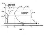
- Fig. 1 depicts a crystallizing set pulse 20 that generally extends from about time To to time T 2 to place the phase change material of a particular cell in the crystalline state.
- the set pulse 20 represents a momentary rise in the temperature of the phase change material.
- the set pulse 20 is to be contrasted to the reset pulse 10, a pulse that is also associated with a higher temperature of the phase change material but may have significantly shorter duration, as the reset pulse 10 extends from about time To to T 1 .
- the reset pulse 10 may be used to transform a phase change material-based memory cell from the crystalline state to the amorphous state, or "reset" the state of the memory cell to "0.”
- the set pulse 20 may be used to set the state of the memory cell to "1.”
- the set heating is slowly removed because this tends to leave the cell in an optimum crystallized set state and allows use of the same peak heating used with reset. For reset the heating must be quenched rapidly to avoid crystallization.
- the reset current is 1.5 times the minimum required to reset a bit with a width of about 50 nsec and a trailing edge under 10 nsec.
- the set current peak and width is about the same as reset, but the trailing edge is preferably much slower and on the order of a microsecond fall time.
- the reset current may be less than 4 ma.
- a current is routed through the memory cell to cause a voltage to develop across the cell.
- This voltage is proportional to the resistance exhibited by the cell.
- a higher voltage indicates that the cell is in the amorphous state, the higher resistance state; and a lower voltage indicates that the cell is in the crystalline state, the lower resistance state.
- the memory cell is deemed to indicate a "1" bit of data when its phase change material is in the crystalline state and indicate a "0" bit of data when its phase change material is in the amorphous state.
- this convention may be reversed, i.e., the memory cell in these embodiments is deemed to indicate a "0" bit of data when its phase change material is in the crystalline phase and indicate a "1" bit of data when its phase change material is in the amorphous phase.
- the non-inverting input terminal of a comparator may be coupled to the cell to receive an indication of the cell voltage produced by forcing a current, such as 10 ⁇ a through the cell.
- the inverting input terminal of the comparator may be coupled to a threshold voltage that serves as a reference for purposes of distinguishing a "1" bit from a "0" bit.
- the comparator compares the cell voltage to this threshold voltage to generate an indication of whether the memory cell stores a "1" bit of data or stores a "0" bit of data. This comparison produces an output signal (indicative of the read bit) and may be stored in a latch or flip-flop.
- the threshold voltage may be formed, for example, by the product of a thresholds resistance (of a threshold resistor) and a current. This current, in turn, may have (for example) the same magnitude as the current that flows through the memory cell during the reading of its stored bit.
- the threshold resistor may have a resistance somewhere between the resistance of the memory cell for a "1" bit of data and the resistance of the memory cell for a "0" bit of data.
- the product of the resistance of the threshold resistor and the current that flows through the threshold resistor produces the threshold voltage, a voltage that is located somewhere between the read voltage of the memory cell when in the amorphous state and the read voltage of the memory cell when in the crystalline state.
- a potential difficulty with the use of the phase change memory cell is that for a number of different possible reasons, the resistance that is exhibited by the cell to indicate a particular memory state may be unacceptably close to a threshold that distinguishes that particular memory state from another memory state.
- the cell may have a resistance that indicates the amorphous state, a memory state that may be associated with the bit "0," for example.
- the resistance of the cell may be close to a threshold resistance that defines the transition between the amorphous and crystalline states.
- the cell's resistance may indicate the crystalline state, a state that may be associated with the bit "1," for example. Therefore, it is generally desirable to have a sufficient margin between the resistance of the cell and the threshold resistance that defines the transition between memory states of the cell.
- An insufficient margin may be caused by the use of incorrect slopes and/or magnitudes by the set pulse and/or the reset pulse; and the insufficient margin may be the result of one or more reads from the memory cell. For example, flowing current through a particular phase change memory cell to read a bit of data from the cell may partially change the resistance exhibited by the cell. As a more specific example, if the memory cell is in the amorphous state (for example), reading data from the cell may partially crystallize the phase change material of the cell, thereby undesirably lowering the resistance that is exhibited by the cell. As a result, the integrity of the memory state that is exhibited by the cell may be compromised, especially if subsequent reads from the cell further change the cell's resistance.
- a memory device of the memory 20 may use a technique 100 that is depicted in Fig. 3 to refresh a particular memory cell.
- a particular memory cell indicates two states.
- a particular memory cell may indicate more than two memory states.
- a margin deficiency between any two of the memory states may be cured by applying the refresh techniques described herein.
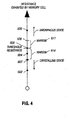
- the memory device determines (block 101) whether the resistance level that is exhibited by the memory cell is within a predefined margin of a resistance threshold level that defines the transition point between the amorphous and crystalline states (i.e., the two states of the memory cell). For example, referring to Fig. 4 , for exhibiting a resistance above a threshold resistance level 605, a particular cell is deemed to be in the amorphous state and thus, indicate a particular data bit (a "0" bit, for example).
- the cell For exhibiting a resistance below the threshold resistance level 605, the cell is deemed to be in the crystalline state and thus, indicate different data bit (a "1" bit, for example).
- the cell is deemed to be in the amorphous state, and for a resistance 602, the cell is deemed to be in the crystalline state.
- the cell For a resistance 604, the cell is in the crystalline state, but the resistance 6C is not outside of an acceptable margin from the threshold resistance level 605.
- the memory device determines (diamond 102) that the exhibited resistance is outside of the predefined margin, then the memory device does not perform the refresh. Otherwise, if within the margin, the memory device prepares to rewrite the memory cell with the current data bit that is indicated by the memory cell to refresh the cell's resistance. That is, if an amorphous state bit is higher in resistance than 605 but less than the resistance 609 of Fig. 4 , then the margin 611 is inadequate and should be refreshed. Similarly, i. a crystalline state bit is less than 605 but greater than 607 in Fig 4 , then the margin 614 is inadequate and should be refreshed.
- the memory device may adjust (block 103) the appropriate parameters for a write of a bit of data to the cell.
- parameters of the set/reset pulse may need to be adjusted to ensure the subsequent rewrite that is involved with the refresh operation establishes the appropriate resistance for the cell. For example, if the cell is supposed to exhibit a low resistance that is associated with a "1" bit of data (for example) but instead exhibits a slightly higher resistance than expected, the slope of the trailing edge of the se current pulse that is used for the rewrite may be increased to ensure that the resistance of the cell is lowered.
- the magnitude of the reset current pulse may be increased in the rewrite to ensure that the cell is correctly reset.
- the bit is rewritte (block 104) to the cell to complete the refresh.
- the chip can be periodically commanded to read all bits on the chip either gradually (intersperses with other reads or writes) or continuously.
- This intentional refresh can be done much like that in a DRAM, and might be done, for example, after every 1 hour of power up time (instead of every few milliseconds for a DRAIN).
- the counting of time can be done on the chip (self-refresh) or externally in the system (by the computer's sequentially working through all bits on the chip).
- the bits might be all read and refreshed if necessary whenever the chip is powered up.
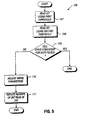
- Fig. 5 depicts a more specific technique 106 that may be used by the memory device to refresh a particular memory cell.
- the technique 106 includes performing two read operations with the memory cell: a first read operation (block 107) in which a first threshold is used to determine the state ("1" or "0") of the memory cell; and a second read operation (block 108) in which a second, more restrictive (lower margin) threshold is used to determine the state of the memory cell.
- the first threshold is the resistance threshold that is used by the memory device in normal read operations and distinguishes the boundary between the crystalline and amorphous states during normal read operations.
- This threshold level is graphically depicted in Fig. 4 as being at reference numeral 605.
- a resistance margin should exist on both sides of the resistance threshold level 605.
- multiple comparators may be used and the bit voltage simultaneously compared to the threshold (to determine if it is a 1 or 0) and also to the margin thresholds (to assure the cell reads with alternate margin). This avoids the delay of another read to determine if an additional write is needed to improve cell margin.
- Determining whether the margin exists is accomplished by the read operation of block 108 in which a second threshold level is used.
- This second threshold level defines the boundary of the margin for the particular memory state detected in the read operation of block 107. For example, if the read operation in block 107 indicates the cell is in the amorphous state, a higher resistance threshold 609 ( Fig. 4 ) is used in the read operation in block 108. The higher threshold 609 defines the boundary of a margin 611. If the read operation in block 107 indicates the cell is in the crystalline state, a lower resistance threshold 607 is used in the read operation in block 108. The lower threshold 607 defines the boundary of a lower margin 614.
- the margin that is established by the second threshold may be about a twenty percent variation (up or down, depending on the memory state detected by the read operation in block 107) from the first threshold, in some embodiments of the invention.
- the memory device performs a refresh of the memory cell by possibly adjusting (block 110) write parameters (as described above in connection with the technique 100) prior to initiating (block 111) the rewriting of the bit read in block 107. Avoiding unnecessary writes is desirable since field endurance is most significantly improved by reducing write cycles.
- the memory device may perform a technique 112, a technique in which, in response to the memory device reading (block 113) a bit from a memory cell, the memory device refreshes (block 114) the memory cell if sufficient margin exists between the cell's exhibited resistance and the threshold resistance used for normal read operations.
- Fig. 7 depicts a technique 115 that the memory device performs in some embodiments of the invention.
- the memory device in response to writing (block 116) a particular bit to a memory cell, refreshes (block 117) the memory cell if sufficient margin exists between the cell's exhibited resistance and the threshold resistance used for normal read operations.
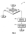
- Fig. 8 depicts another technique 118 that the memory device performs in connection with a write operation to a particular memory cell, in some embodiments of the invention.
- the memory device determines (diamond 119) whether both the memory state of the memory cell is consistent with the bit of data to be written to the memory cell and a sufficient margin exists between the cell's exhibited resistance and the threshold resistance used for normal read operations. If this condition is true, then the memory device does not perform the write operation to the memory cell, as the correct bit is already stored in the memory cell and sufficient margin exists. Otherwise, the memory device writes (block 120) the new bit to the memory cell and refreshes (block 121) the memory cell if needed to ensure a sufficient margin exists between the cell's exhibited resistance and the threshold resistance used for normal read operations.
- Fig. 9 depicts a particular memory device 33 of the memory 32 in accordance with some embodiments of the invention.
- the specific structure of the memory device 33 is depicted for purposes of describing some out of many possible embodiments of the invention. It is understood that other and different structures may be used, as the scope of the invention is defined by the appended claims.
- the memory device 33 may perform one or more of the techniques described above in connection with Figs. 3 and 5-8.
- the memory device 33 may be programmed to first read a bit before writing it. If the bit is already in the desired state to be written, the write cycle is skipped (but only if the margin is still adequate). This will improve field reliability because reliability for a given bit is often related to the total number of write cycles it experiences. For field requests to program a bit to a state that the bit is already in as determined by a pre-read before write, ignoring that request after reading and confirming margin will improve reliability since a read operation has far less effect on experienced field reliability compared to a write operations
- the minimum reset current necessary to write bits in a block may be logged by total or by percentage. Once a certain number is exceeded, thereafter the minimum reset current attempted for a reset or set shall be increased to this level. Preferably, the reset current will start at this minimum level and, especially for trying to reset the bit, the current will be increased in small increments until the bit is satisfactorily written with adequate margin.
- a technique 700 that is depicted in Fig. 14 may be used to determine the current level to be used for resetting cells of a particular block.
- the term "block” refers to the smallest section of the memory device that shares a threshold sensor (a comparator, for example).
- the memory device 33 resets (block 702) the next cell in the block using a predetermined current level for the reset operation. For each initial attempt to reset a particular cell and establish an acceptable margin for the cell, the reset current level is set to a minimum level and thereafter upwardly adjusted for subsequent attempts, as described below. As described below, the minimum reset current may be adjusted after all cells of the block are written.
- the memory device 33 determines (diamond 704) whether there is a sufficient margin after the reset operation. If not, the memory device 33 increases (block 706) the current level and returns to block 702. Otherwise, the memory device 33 increments (block 710) an appropriate counter to log the current reset current level. In this manner, the memory device 33 may include counters 409 (see Fig. 9 ), each of which is associated with a particular reset current range. By incrementing the appropriate counter, the current that is sufficient to reset a particular cell and ensure the cell has an appropriate margin is logged. In this manner, by examining the log of currents used to reset the cells in a particular block, the memory device 33 may then base a decision of whether to increase the minimum reset current level.
- the memory device 33 may determine (diamond 714) whether a significant number of cells have been reset using a current that is higher than the minimum current level. If so, then the memory device 33 adjusts (block 716) the minimum current level for reset operations and stores this in a predefined location in the memory device 33. For example, this predefined location may be a row of their only accessible by a control circuit 400 ( Fig. 9 ) of the memory device 33.
- a preferred sequence may be to perform a write reset operation at current X, and then read to be sure that the reset operation is done with adequate margin. If not, the cell is written at (1.1)X, and then read to determine if adequate margin. If there is not an adequate margin, then the cell is written at (1.2)X, read again, etc. Hence the reset becomes a series of reset sweeps of increasing current until the bit is written with adequate margin. The successful current is logged by incrementing a counter for that current. When enough bits are writing at a higher current (adding all the currents of higher value), the lowest starting current is incremented for future writes. This information can be stored in the non-volatile phase change memory in a special row accessed by the memory device 33 and not by the user (other than for test purposes).
- a technique 780 that is depicted in Fig. 15 may be used to establish a minimum fall sweep time for a write set operation.
- the memory device 33 sets (block 782) the next cell in a block using a predetermined sweep fall time. For each initial attempt to set a particular cell and establish an acceptable margin for the cell, the sweep fall time is set to a minimum time and thereafter upwardly adjusted, as described below. As described below, the minimum time may be adjusted after all cells of the block are written.
- the memory device 33 determines (block 784) whether the margin is sufficient. If not, the sweep fall time is increased (block 786), and control returns to block 782. Otherwise, the memory device 33 increments (block 790) an appropriate counter 409 ( Fig. 9 ) to log the sweep fall time. If the memory device 33 determines (diamond 792) that more bits are in the block to process, then control returns to block 782. Otherwise, the memory device 33 determines (diamond 794) whether a significant number of bits have been written using sweep fall times greater than the minimum sweep fall time. If so, then the memory device 33 adjusts (block 796) the sweep fall time and stores it in the memory accessible by the control device 419.
- a particular set begins at the current minimum reset current level.
- the set sweep fall is increased time by 20%. If this is unsuccessful, the set current is increased by 20%, and then the set operation is repeated at the higher set sweep time.
- a counter 409 is incremented to reflect the successful current if greater than minimum.
- the set sweep counter 409 is incremented if the amount of set sweep time is increased.
- the magnitude of this current is varied in a binary or linear search using currents successively less than I reset until a current is found that sets the resistance in read mode in the desired range.
- a counter may be incremented so a more intelligent starting current may be defined for that block or chip, perhaps starting the initial current at 150 percent of the most frequent successful Iset current, and indexing lower from there. This technique is most preferable when writing multiple levels into the cell.
- the chip is scanned by block (the smallest section of memory that shares a threshold sensor).
- the minimum reset current is found that successfully writes all bits in the array with adequate margin. This current is then increased an adequate amount, preferably about 20% for subsequent writes in that block.
- the minimum set sweep slope is then found using this chosen value of reset current that will set all bits in the block. Then, this slope is increased preferably by 50% to assure adequate margin for setting bits.
- both set sweep slope fall time and reset current are checked at the factory at both high and low temperatures. This procedure is followed for all blocks on the chip.
- the memory device 33 includes memory cells 140 that are addressed via column lines 130 and row lines 132, as can be appreciated by those skilled in the art.
- Each memory cell 140 includes a phase change material whose state is controlled by write preset/set cycles to store an associated bit of data.
- a 4X4 block 139 of the memory cells 140 is depicted in Fig. 9 , it is understood that this array size is used to simplify the proceeding discussion.
- the memory device 33 may have a significantly larger or smaller array of memory cells 140.
- each memory cell 140 is associated with a particular column line 130 (also called a "bit line") and a particular row line 132, and the activation of the associated column 130 and row 132 lines selects the cell 140 for a write or read operation.
- the memory cell 140 may be coupled to its associated column line 130 and may be coupled through what is effectively a diode 142 (preferably a PNP bipolar junction transistor (BJT) where size is important, for example) to its associated row line 132. Therefore, when a particular memory cell 140 is selected, its associated column line 130 is driven high and its associated row line 132 is driven low, a condition that causes a current pulse to flow through the memory cell 140. It is the magnitude and duration of this current pulse that establishes whether the selected memory cell 140 is being read, set (via a write set pulse) or reset (via a write reset pulse).
- BJT PNP bipolar junction transistor
- the row decoder 124 In response to address signals (called A0, A1, WB0 and WB1), the row decoder 124 selects one, two or four row lines 132. In this manner, the row decoder 124, in response to these address signals, selectively drives row select signals (called X0, X1, X2 and X3) low to select one or more of the row lines 132. As an example, a certain combination of the address signals may cause the row decoder 124 to select two of the row lines, another combination of the address signals may cause the row decoder 124 to select one of the row lines 132, another combination of the address signals may cause the row decoder 124 to select four of the row lines 132, etc. When the row decoder 124 drives the row line(s) 132 low, this enables a read or write cycle to occur to one or more memory cells 140, depending on the selections by the column decoder 122.
- the column decoder 122 in response to its received address selection signals (called A2, A3, WB3 and WB2) drives column select signals (called Y0, Y1, Y2 and Y3) high to select one or more column lines 130. In this manner, when one of the column select signals is driven high, the corresponding column line 130 has been selected. Similar to the row decoder 124, the column decoder 122 may select one, two or four column lines 130. Thus, the selection of the column line(s) by the column decoder 122 and the row line(s) 132 by the row decoder 124 addresses selected memory cells 140 and may be used to address a block of the memory cells 140.
- the column decoder 122 receives signals called QUENCH and SET_SLOPE.
- the SET_SLOPE signal establishes a trailing slope(s) for set pulse(s) that set selected particular memory cells(s). In this manner, when the SET_SLOPE signal is asserted (driven high, for example) during a write set cycle, the column decoder 122 imparts a trailing edge on the set pulse, as described further below, that is preferably greater than 500 nsec for the trailing edge fall time.
- the column decoder 122 does not add this trailing edge, resulting in a reset bit by quickly terminating the reset current with a trailing edge that is preferably less than 10 nsec.
- the QUENCH signal is used to control the time at which the set or reset pulse ends. In this manner, in response to the QUENCH signal being asserted (driven high, for example), the column decoder 122 ends the current reset/set pulses. Conversely, in response to the QUENCH signal being deasserted, the column decoder 122 allows the current reset or set pulses (if occurring) to continue.
- the QUENCH signal may be used to end the slope established by the SET_SLOPE signal during a write set cycle once it has passed the critical set slope crystallization current (about 30% of the current required to reset a bit).
- Fig. 10 depicts a truth table 110 that illustrates the selection of the row select signals X0, X1, X2 and X3 in response to various states for the address decode signals A0, A1, WB0 and WB1.
- the row decoder 120 drives only the X3 row select signal to select one corresponding row line 132.
- Other individual row lines 132 may be selected by combinations of the A0 and A1 signals, as depicted in rows 1-4 of the truth table 110.
- Rows 5 and 6 of the truth table 110 depict combinations possible when the WB0 signal is driven high and the WB1 signal is driven low. As shown, for these states, two row lines 132 are selected, and the two particular row lines that are selected depend on the state of the A1 signal. When both the WB0 and WB1 signals are driven high, then all of the row lines 132 are selected, as depicted in line 7 of the truth table 110. Other combinations may be used to select the rows 132.
- Fig. 11 depicts one out of many possible embodiments for the column decoder 122.
- the column decoder 122 includes drive circuits 150 (drive circuits 150a, 150b, 154c and 150d, as examples), each of which is associated with a different column line 130.
- a particular drive circuit 150 is activated for purposes of selecting and reading/writing data from one or more cells 140 of its associated column line 130 in response to a signal that is provided by a decode circuit 180.
- the decode circuit 180 receives the column address signals A2, A3, WB2 and WB3 and furnishes decode signals called DECY0, DECY1, DECY2 and DECY3 that are used to activate the decode circuits 150a, 150b, 150c and 150d, respectively.
- the drive circuit 150a is activated in response to the assertion of the DECY0 signal by the decode circuit 180.
- the drive circuit 150 may have the circuitry that is illustrated in Fig. 11 for the drive circuit 150a.
- the drive circuit 150 may include a P-channel metal-oxide-semiconductor field-effect-transistor (PMOSFET) 154 that has its source terminal coupled to a positive voltage supply (called V DD ) and its drain terminal coupled to the source terminal of a PMOSFET 158.
- V DD positive voltage supply
- the drain terminal of the PMOSFET 158 is coupled to the column line 130 that is associated with the drive circuit 150.
- the gate terminal of the PMOSFET 154 receives the corresponding decode signal (DECY0, DECY1, DECY2 or DECY3) from the decode circuit 180.
- the gate terminal of the PMOSFET 154 receives the DECY0 signal.
- this signal is asserted (driven high, for example) the source-drain path of the PMOSFET 154 conducts a current that, in a write cycle, is established by the PMOSFET 158.
- the gate terminal of the PMOSFET 158 receives a current sense signal (called S2) that establishes the current through the source-drain path of the PMOSFET 154, the source-drain path of the PMOSFET 158 and the current that flows into the associated column line 130.
- S2 a current sense signal
- the source-drain paths of the PMOSFETs 154 and 158 are serially coupled together with the column line 130 during the write operation.
- the column decoder 122 adjusts the magnitude of the S2 signal so that each activated drive circuit 150 provides more current to its associated column line 130 when two memory cells 140 per selected column line 130 are being written than when one memory cell 140 per selected column line 130 is being written. Furthermore, in response to the selection of four memory cells 140 per column line 130, the column decoder 122 adjusts the magnitude of the S2 signal so that more current is applied to the selected column line 130 than when one or two memory cells per selected column line 130 are being written.
- the drive circuit 150 includes a PMOSFET 156 to route the read current to the associated column line 130.
- the source terminal of PMOSFET 156 is coupled to the drain terminal of the PMOSFET 154, and the drain terminal of the PMOSFET 156 is coupled to the column line 130 that is associated with the drive circuit 150.
- the gate terminal of PMOSFET 156 receives a current sense called S1.
- the column decoder 122 adjusts the magnitude of the S1 signal to adjust the level of current that flows through the associated column line 130 during a read operation, as the source-drain of the PMOSFET 156 is coupled in series with the drain-source path of the PMOSFET 154 and the column line 130.
- Each drive circuit 150 may also include an NMOSFET 157 that has its drain-source path coupled between the associated column line 130 and ground.
- the gate terminal of the NMOSFET 157 receives a reset signal (called RESET), a signal that is asserted (driven high, for example) after a read operation to discharge energy stored due to the capacitance of the column line 130.
- RESET reset signal
- the other drive circuits 150b, 150c and 150d may have similar designs, in some embodiments of the invention. Other designs are possible for the drive circuit 150, in other embodiments of the invention.
- the column decoder 122 includes the following circuitry.
- This circuitry includes a PMOSFET 186 that has its gate terminal coupled to ground.
- the source terminal of the PMOSFET 186 is coupled to a positive supply voltage (called V DD ), and the drain terminal of the PMOSFET 186 is coupled to the source terminal of a PMOSFET 184.
- the gate and drain terminals of the PMOSFET 184 are coupled together to furnish the S2 signal. These terminals are also coupled to one terminal of a resistor 188.
- the other terminal of the resistor 188 is coupled to the drain terminal of an N-channel MOSFET (NMOSFET) 194 that has its source terminal coupled to ground.
- the gate terminal of the NMOSFET 194 receives a signal called W4.
- the NMOSFET 194 conducts, as determined by the resistance of the resister 188, a current that flows through the PMOSFETs 184 and 186. This current, in turn establishes the level of the S2 signal that, in turn, establishes the current that flows through the selected column lines 130.
- the resistor 188 and the PMOSFET 194 are part of a pulse circuit 200.
- the column decoder 122 includes three such pulse circuits 200a, 200b and 200c.
- the differences between the pulse circuits 200 are established by the value of the resistance 188 and the signal received at the gate terminal of the NMOSFET 194.
- the slope circuit 200b receives a signal called W2
- the slope circuit 200c receives a signal called W1.
- the pulse circuit 200c is used to set the current through the column line 130.
- both the W1 and W2 signals are asserted (driven high, for example) to cause twice the level of current to flow than when one memory cell 140 per column line 130 is written through the select column line 130.
- the W1, W2, and W4 signals are all asserted (driven high, for example) to cause additional current to flow through the selected column lines 130.
- the resistances of the resistors 188 in each of the pulse circuits 200 have the appropriate values to implement the necessary binary weighting of the current among the pulse circuits 200.
- each pulse circuit 200 includes an NMOSFET 190 and a capacitor 192.
- the gate terminal of the NMOSFET 190 receives the SET_SLOPE signal, and the source terminal of the NMOSFET 190 is coupled to ground.
- the drain terminal of the NMOSFET 190 is coupled to one terminal of the capacitor 192, and the other terminal of the capacitor 192 is coupled to the drain terminal of the MOSFET 194.
- the SET_SLOPE signal is asserted to cause both terminals of the capacitor 192 to be coupled to ground. Therefore, when the MOSFET 194 de-activated, the capacitor 192 introduces a time constant to produce the trailing edge of the set pulse. The end of the set pulse may be controlled via the assertion of the QUENCH signal to terminate the cycle early to save write time.
- the reset pulse is created by leaving the SET SLOPE signal unasserted and the end of the reset pulse is controlled via the QUENCH signal, preferably using an undecoded n-chan pulldown on each column to rapidly pull the column to ground to assure rapid termination of the write cycle trailing edge in under 10 nsec.
- the column decoder 122 includes a PMOSFET 230 that has its source coupled to the V DD supply voltage and its gate terminal coupled to ground.
- the drain terminal of the PMOSFET 230 is coupled to the source terminal of a PMOSFET 232.
- the gate and drain terminals of the PMOSFET 232 are coupled to one terminal of a resistor 236 and furnish the S1 signal.
- the other terminal of the resistor 236 is coupled to the drain terminal of an NMOSFET 234, and the source terminal of the PMOSFET 234 is coupled to ground.
- the gate terminal of the NMOSFET 234 receives a signal (called R) that is asserted (driven high, for example) in response to a read operation.
- R a signal
- the read mirror formed from the PMOSFETs 230 and 232 forms (via the S1 signal) a read current in selected column line(s) 130.
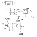
- Each bit, or column line 130 is coupled to associated read path circuitry 499 that is used by the memory device 33 to detect and store a bit that of data that appears on the column line 130 during a read operation.
- the read path circuitry 499 includes a comparator 500 to, in response to a read operation, compare the resistance exhibited by the associated memory cell 140 with a resistive threshold that is established by a threshold current source 516 and a resistor 508.
- the non-inverting input terminal of the comparator 500 is be coupled to the column line 130, and the inverting input terminal of the comparator 500 is coupled to a current communication line 502 that conducts a current (called I T ) that is furnished by the threshold current source 516.
- One terminal of the resistor 508 is coupled to the current line 502, and the other terminal of the resistor 508 is coupled to the emitter terminal of a PNP BJT 510.
- the base terminal of the BJT 510 is coupled to ground, and the collector terminal of the BJT 501 is coupled to ground. Due to this arrangement, the BJT 510 effectively forms a diode between the resistor 508 and ground.
- the non-inverting input terminal of the comparator 500 receives an indication of the voltage across the memory cell 140
- the inverting input terminal of the comparator 500 receives an indication of the voltage across the resistor 508.
- the voltage drop across the diode 142 is canceled out by the voltage drop across the BJT 510 in the comparison formed by the comparator 500.
- the comparator 500 effectively compares a resistive threshold (indicated by the voltage at the inverting input terminal produced by the product of the I T current and the resistance of the resistor 508) with the resistance of memory cell 140 (indicated by the voltage (at the non-inverting input terminal) that is produced by the resistance exhibited by the memory cell 140 and a read current (called I C ) that flows through the column line 130 during a read operation).
- the resistance threshold may be changed by either changing the I T current or by changing the value of the resistance 508.
- the threshold current source 516 (under the control of the control circuit 400 ( Fig. 9 ) of the memory device 33 via control lines 514) regulates the resistance threshold by regulating the level of the I T current.
- the threshold current switch 516 may set the level of the I T current to the same level as the I C current.
- the inverting input terminal of the comparator 500 is set somewhere between the low and high voltages present at the non-inverting input terminal of the comparator 500.
- the comparator 500 asserts its signal to indicate a "0" bit (for example), and for the crystalline state of the memory cell 140, the comparator 500 de-asserts its output signal to indicate another memory state (i.e., the "1" bit).
- the threshold current source 516 increases or decreases the I T current appropriately to change the resistive threshold. For example, if in a read operation in which the I T and I C current levels are approximately the same, the comparator 500 detects an amorphous state for the memory cell 140 during the read operation 107 ( Fig. 5 ), then the threshold currents source 516 may be used (under the control of the control circuit 400) to increase the threshold by increasing the I T current in the subsequent read operation 108 ( Fig. 5 ). Similarly, if the comparator 500 detects a crystalline state for the memory cell 140 in the read operation 107 ( Fig. 5 ), the threshold current source 516 may be controlled by the control circuit 400 to decrease the I T current to effectively decrease the resistant threshold during the subsequent read operation 108 ( Fig. 8 ).
- the circuitry 499 may include a D-type flip-flop 504 that stores the state of the output signal of the comparator 500 in response to an edge of a clock signal (called CLK).
- CLK clock signal
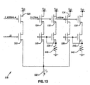
- the threshold current source 516 includes a PMOSFET 520 that has its source terminal coupled to a positive supply voltage called V DD .
- the drain terminal of the PMOSFET 520 is coupled to the source terminal of another PMOSFET 522.
- the drain terminal of the PMOSFET 522 is coupled to the current communication line 502.
- the gate terminal of the PMOSFET 520 receives a signal called S_NORMAL#, and the gate terminal of the PMOSFET 522 receives the S1 signal. Due to this arrangement, during a normal read operation 107 ( Fig. 7 ) when the margin is not being checked, the S_NORMAL# signal is asserted (driven low, for example) to activate the PMOSFET 520.
- the level of current that flows through the source-drain path of the PMOSFET 520 is set by the PMOSFET 522, as controlled by the S1 signal.
- the threshold current source 516 contains additional circuitry to control the level of the I T current during a read operation where the threshold is lowered for purposes of checking the margin for the cell when the cell is in the crystalline state.
- this circuitry includes a PMOSFET 524 that has its source terminal coupled to the V DD supply voltage.
- the gate terminal of the PMOSFET 524 receives a signal called S_LOW#.
- the drain terminal of the PMOSFET 524 is coupled to the source terminal of another PMOSFET 526, and the drain terminal of the PMOSFET 526 is coupled to the current communication line 502.
- the S_LOW# signal is asserted (driven low, for example) to cause the source-drain path of the PMOSFET 524 to conduct.
- the level of this current is set by the PMOSFET 526.
- the PMOSFET 526 is coupled in a current mirror arrangement with a PMOSFET 528. In this manner, the gate terminals of the PMOSFETs 526 and 528 are coupled together, and the gate terminal of the PMOSFET 528 is coupled to its drain terminal resistor 530 is coupled between the drain terminal of the PMOSFET 528 and ground.
- the source-drain path of a PMOSFET 532 is coupled between the V DD supply voltage and the source terminal of the PMOSFET 528.
- the gate terminal of the PMOSFET 532 is coupled to the gate terminal of the MOSFET 524.
- the value of the resistance 530 may be chosen to lower the resistance threshold.
- the threshold current source 516 may also include, in some embodiments of the invention, circuitry to raise the I T current level to check the margin when the memory cell is in the amorphous state.
- the current source 516 may include a PMOSFET 536 that has its drain terminal coupled to the current communication line 502.
- the source terminal of the PMOSFET 536 is coupled to the drain terminal of a PMOSFET 534.
- the source terminal of the PMOSFET 534 is coupled to the V DD supply voltage.
- the gate terminal of the PMOSFET 534 receives a signal called S_HIGH#, a signal that is asserted (driven low, for example) to indicate the increase resistive threshold.
- S_HIGH# a signal that is asserted (driven low, for example) to indicate the increase resistive threshold.
- the PMOSFET 536 is coupled in a current mirror arrangement with a PMOSFET 540.
- the gate terminals of the PMOSFETs 536 and 540 are coupled together, and the gate terminal of the PMOSFET 540 is coupled to its drain terminal.
- a resistor 542 is coupled between the drain terminal and ground.
- the source-drain path of a PMOSFET 538 is coupled between the V DD supply voltage and the source terminal of the PMOSFET 540.
- the gate terminals of the PMOSFETs 534 and 538 are-coupled together.
- the memory device 33 may include the control circuit 400 to generate signals to control such cycles in the memory device 33 as the read cycles, write preset cycles and write reset cycles.
- the control circuit 400 also initiates the read operation 108 compares (diamond 102) the bits during a margin check and controls the threshold current source to select the resistance threshold used during a particular read operation.
- the control circuit 400 receives signals (via input lines 401) from the memory bus 36 indicative of potential addresses and commands that involve the memory device 33. Ln this manner, the control circuit 300 may decode a burst write operation and generate the appropriate signals to control the storage of data associated with the burst write operation in targeted memory cells 140 of the memory device 33.
- the memory device 33 may also include additional circuitry, such as, for example, a data buffer 402 to temporarily store the data flowing into and out of the memory device 33 and communicates data to the memory bus 36 via data communication lines 405.
- the memory device 33 may also include an address buffer 408 that communicates with the memory bus via communication lines 407.
- the address buffer 408 shares the addresses associated with memory operations as well as decodes the addresses and to some extent may generate the address signals (on the communication lines 410) that are provided to the row 124 and column 122 decoders.
- the control circuit 400 also increments the counters 409 as appropriate and stores minimum set sweep fall times and reset current levels in the memory of the device 33.
- the computer system 30 may include other components than the memory controller hub 34 and the memory 32.
- the computer system 30 may include a processor 42 (one or more microprocessors or controllers, as examples) that is coupled to a system bus 40.
- the system bus 40 is coupled to the memory controller hub 34 along with an Accelerated Graphics Port (AGP) bus 44.
- AGP Accelerated Graphics Port
- the AGP is described in detail in the Accelerated Graphics Port Interface Specification, Revision 1.0, published on July 31, 1996, by Intel Corporation of Santa Clara, California.
- the computer system 30 may also include a display controller 46 that is coupled to the AGP bus 44 and generates signals to drive a display 48.
- the memory controller hub 34 is also coupled (via a hub interface 50) to an input/output (I/O) hub 52.
- the I/O hub 52 may provide interfaces to, for example a Peripheral Component Interconnect (PCI) bus 54 and an expansion bus 62.
- PCI Peripheral Component Interconnect
- the PCI Specification is available from The PCI Special Interest Group, Portland, Oregon 97214.
- the PCI bus 54 may be coupled to a network interface card (NIC) 56, and the I/O controller 64 may receive input from a mouse 66, and the I/O controller 64 may receive input from a mouse 66 and a keyboard 68, as well as control operation of a floppy disk drive 70.
- the I/O hub 52 may also control operation of a CD-ROM drive 58 and control operation of a hard disk drive 60.
- the memory controller hub 34 may include a memory controller 35.
- the memory controller 35 serves as an interface between the memory bus 36 and the PCI 54, system 40 and AGP 44 buses.
- the memory controller 35 generates signals to indicate the control signals, address signals and data signals that are associated with a particular write or read operation that targets cells of the phase change material memory 32.
Abstract
Description
- This invention generally relates to electronic memories, and more particularly, the invention relates to refreshing memory cells of a phase change material memory device.
- A phase change material may be used to store the memory state of a memory cell of a semiconductor memory device. In this manner, phase change materials that are used in phase change material memory devices may exhibit at least two different states. The states may be called the amorphous and crystalline states. Transitions between these states may be selectively initiated. The states may be distinguished because the amorphous state generally exhibits higher resistivity than the crystalline state. The amorphous state involves a more disordered atomic structure. Generally any phase change material may be utilized to exhibit these two states. However, as an example, thin-film chalcogenide alloy materials may be particularly suitable.
- The phase change may be induced reversibly. Therefore, the phase change material may change from the amorphous to the crystalline state and may revert back to the amorphous state thereafter, or vice versa, in response to temperature changes. In effect, when the phase change material is used in a memory cell, the memory cell may be thought of as a programmable resistor, which reversibly changes between higher and lower resistance states. The phase change may be induced by resistive heating that is caused by a current that flows through the material.
-
US 5,296,716 discloses a solid state, directly overwritable, electronic, non-volatile, high density, low energy, high speed, multibit single cell memory based upon phenomenologically novel electrical switching characteristics wherein the memory exhibits higher switching speeds at reduced energy levels.US 6,108,241 discloses a method of leakage detection for cells in a flash memory device.US 6,151,246 addresses the problem of providing a multibit-per-cell memory that is resistant to data errors by dividing a range of possible threshold voltages into allowed states associated with data values and forbidden zones between the allowed states wherein a memory cell being written is programmed into an allowed state. -
US 5.896.318 discloses a method and apparatus for protesting content of semiconductor non-volatile memory and memory itself which refreshes memory bits which have drifted in a way that data inversion may occur, thus increasing lifetime and availability of the memory. - A method and a memory device according to the invention are defined respectively by
claims 1 and 8. -
-
Fig.1 depicts temperature waveforms for setting and resetting a memory cell of a phase change material memory device. -
Fig. 2 is a schematic diagram of a computer system according to an embodiment of the invention. -
Figs. 3 and5 are flow diagrams depicting techniques to refresh a phase change memory cell according to embodiments of the invention. -
Fig. 4 is an illustration of a resistance exhibited by a phase change memory cell. -
Fig. 6 is a flow diagram depicting a technique to read a bit of data from a phase change memory cell according to an embodiment of the invention. -
Figs. 7 and8 are flow diagrams depicting techniques to write a bit of data to a phase change memory cell according to embodiments of the invention. -
Fig. 9 is a schematic diagram of a phase change material memory device according to an embodiment of the invention. -
Fig. 10 is a truth table associated with a row decoder of the phase change material memory device ofFig. 9 according to an embodiment of the invention. -
Fig. 11 is a schematic diagram of a column decoder of the phase change material memory device ofFig. 9 according to an embodiment of the invention. -
Fig. 12 is a schematic diagram of read path circuitry for a particular column line according to an embodiment of the invention. -
Fig. 13 is a schematic diagram of a threshold current source of the circuitry ofFig. 12 . -
Fig. 14 is a flow diagram depicting a technique to determine a current to be used for write reset operations. -
Fig. 15 is a flow diagram depicting a technique to determine a sweep fall time to be used for write set operations. - Referring to
Fig. 2 , anembodiment 30 of a computer system in accordance with the invention includes a phase changematerial memory 32 that communicates with amemory controller hub 34 via amemory bus 36. Thememory bus 36 includes communication lines for communicating data to and from thememory 32 as well as control and address lines for controlling the storage and retrieval of data to and from thememory 32. A particular write or read operation may involve concurrently writing data to or reading data from several devices ofmemory 32. - As an example, in some embodiments of the invention, the phase change
material memory 32 may include various memory devices (semiconductor memory chips, or packages, for example), each of which includes phase change material-based memory cells. As an example, each memory cell of a particular memory device may include a phase change material (a thin-film chalcogenide alloy material, for example) that exhibits crystalline and amorphous phases. These states, in turn, are used to indicate the memory states ("1" and "0" states, for example) of the memory cell. - The memory cell of a phase change memory device is not limited to just two memory states (i.e., a"1" state and a "0" state), but instead the memory cell may have a large number of states. That is because each state may be distinguished by its resistance, a number of resistance determined states may be possible, allowing the storage of multiple bits of data in a single memory cell.
- A variety of phase change alloys are known. Generally, chalcogenide alloys contain one or more elements from Column VI of the periodic table. One particularly suitable group of alloys is the GeSbTe alloys.
- For purposes of writing a bit of data to a phase change memory cell, the cell may be either set (to store a "1" bit of data, for example) via a current pulse called a set current pulse or reset via a current pulse (to store a "0" bit of data, for example) called a reset pulse. As an example,
Fig. 1 depicts a crystallizingset pulse 20 that generally extends from about time To to time T2 to place the phase change material of a particular cell in the crystalline state. As shown, theset pulse 20 represents a momentary rise in the temperature of the phase change material. - The
set pulse 20 is to be contrasted to thereset pulse 10, a pulse that is also associated with a higher temperature of the phase change material but may have significantly shorter duration, as thereset pulse 10 extends from about time To to T1. Thus, thereset pulse 10 may be used to transform a phase change material-based memory cell from the crystalline state to the amorphous state, or "reset" the state of the memory cell to "0." In contrast, theset pulse 20 may be used to set the state of the memory cell to "1." Preferably, the set heating is slowly removed because this tends to leave the cell in an optimum crystallized set state and allows use of the same peak heating used with reset. For reset the heating must be quenched rapidly to avoid crystallization. Since the heating is done with current, preferably the reset current is 1.5 times the minimum required to reset a bit with a width of about 50 nsec and a trailing edge under 10 nsec. The set current peak and width is about the same as reset, but the trailing edge is preferably much slower and on the order of a microsecond fall time. These timings and the magnitude of the reset current will vary with the phase change material selected and size and type of electrodes on each side of the material. Preferably, with a contact less than 0.05u, electrodes of TiAlN, and side spacers of nitride, the reset current may be less than 4 ma. - For purposes of reading the bit of data that is stored in the phase change memory cell, a current is routed through the memory cell to cause a voltage to develop across the cell. This voltage, in turn, is proportional to the resistance exhibited by the cell. Thus, a higher voltage indicates that the cell is in the amorphous state, the higher resistance state; and a lower voltage indicates that the cell is in the crystalline state, the lower resistance state.
- It is assumed herein that the memory cell is deemed to indicate a "1" bit of data when its phase change material is in the crystalline state and indicate a "0" bit of data when its phase change material is in the amorphous state. However, it is noted, that in other embodiments of the invention, this convention may be reversed, i.e., the memory cell in these embodiments is deemed to indicate a "0" bit of data when its phase change material is in the crystalline phase and indicate a "1" bit of data when its phase change material is in the amorphous phase.
- For purposes of detecting the memory state of a particular cell, the non-inverting input terminal of a comparator may be coupled to the cell to receive an indication of the cell voltage produced by forcing a current, such as 10 µa through the cell. As an example, the inverting input terminal of the comparator may be coupled to a threshold voltage that serves as a reference for purposes of distinguishing a "1" bit from a "0" bit. Thus, the comparator compares the cell voltage to this threshold voltage to generate an indication of whether the memory cell stores a "1" bit of data or stores a "0" bit of data. This comparison produces an output signal (indicative of the read bit) and may be stored in a latch or flip-flop.
- The threshold voltage may be formed, for example, by the product of a thresholds resistance (of a threshold resistor) and a current. This current, in turn, may have (for example) the same magnitude as the current that flows through the memory cell during the reading of its stored bit. In this manner, the threshold resistor may have a resistance somewhere between the resistance of the memory cell for a "1" bit of data and the resistance of the memory cell for a "0" bit of data. Thus, the product of the resistance of the threshold resistor and the current that flows through the threshold resistor produces the threshold voltage, a voltage that is located somewhere between the read voltage of the memory cell when in the amorphous state and the read voltage of the memory cell when in the crystalline state.
- A potential difficulty with the use of the phase change memory cell is that for a number of different possible reasons, the resistance that is exhibited by the cell to indicate a particular memory state may be unacceptably close to a threshold that distinguishes that particular memory state from another memory state. For example, for a two memory state cell, the cell may have a resistance that indicates the amorphous state, a memory state that may be associated with the bit "0," for example. However, the resistance of the cell may be close to a threshold resistance that defines the transition between the amorphous and crystalline states. Thus, if an inadvertent slight change occurs in the cell's resistance, the cell's resistance may indicate the crystalline state, a state that may be associated with the bit "1," for example. Therefore, it is generally desirable to have a sufficient margin between the resistance of the cell and the threshold resistance that defines the transition between memory states of the cell.
- An insufficient margin may be caused by the use of incorrect slopes and/or magnitudes by the set pulse and/or the reset pulse; and the insufficient margin may be the result of one or more reads from the memory cell. For example, flowing current through a particular phase change memory cell to read a bit of data from the cell may partially change the resistance exhibited by the cell. As a more specific example, if the memory cell is in the amorphous state (for example), reading data from the cell may partially crystallize the phase change material of the cell, thereby undesirably lowering the resistance that is exhibited by the cell. As a result, the integrity of the memory state that is exhibited by the cell may be compromised, especially if subsequent reads from the cell further change the cell's resistance.
- Thus, it is possible that the resistance that is exhibited by the phase change memory cell to indicate a "1" or "0" bit may be too large (for the crystalline state) or too small (for the amorphous state) for a sufficient margin to exist between the exhibited resistance and a threshold resistance that defines the separation point between the amorphous and crystalline states. For purposes of curing this margin deficiency, in accordance with some embodiments of the invention, a memory device of the
memory 20 may use atechnique 100 that is depicted inFig. 3 to refresh a particular memory cell. For purposes of simplifying the following discussion, it is assumed that a particular memory cell indicates two states. However, in other embodiments of the invention, a particular memory cell may indicate more than two memory states. However, regardless of the number of memory states, a margin deficiency between any two of the memory states may be cured by applying the refresh techniques described herein. - Referring to
Fig. 3 , pursuant to thetechnique 100, for purposes of performing a refresh of a particular memory cell, the memory device determines (block 101) whether the resistance level that is exhibited by the memory cell is within a predefined margin of a resistance threshold level that defines the transition point between the amorphous and crystalline states (i.e., the two states of the memory cell). For example, referring toFig. 4 , for exhibiting a resistance above athreshold resistance level 605, a particular cell is deemed to be in the amorphous state and thus, indicate a particular data bit (a "0" bit, for example). For exhibiting a resistance below thethreshold resistance level 605, the cell is deemed to be in the crystalline state and thus, indicate different data bit (a "1" bit, for example). As more specific examples, for aresistance 600, the cell is deemed to be in the amorphous state, and for aresistance 602, the cell is deemed to be in the crystalline state. For aresistance 604, the cell is in the crystalline state, but the resistance 6C is not outside of an acceptable margin from thethreshold resistance level 605. - Referring back to
Fig. 3 , if the memory device determines (diamond 102) that the exhibited resistance is outside of the predefined margin, then the memory device does not perform the refresh. Otherwise, if within the margin, the memory device prepares to rewrite the memory cell with the current data bit that is indicated by the memory cell to refresh the cell's resistance. That is, if an amorphous state bit is higher in resistance than 605 but less than theresistance 609 ofFig. 4 , then themargin 611 is inadequate and should be refreshed. Similarly, i. a crystalline state bit is less than 605 but greater than 607 inFig 4 , then themargin 614 is inadequate and should be refreshed. - In this manner, in this preparation, the memory device may adjust (block 103) the appropriate parameters for a write of a bit of data to the cell As further described below, if the refresh is needed just after a bit of data has been written to the cell, then parameters of the set/reset pulse may need to be adjusted to ensure the subsequent rewrite that is involved with the refresh operation establishes the appropriate resistance for the cell. For example, if the cell is supposed to exhibit a low resistance that is associated with a "1" bit of data (for example) but instead exhibits a slightly higher resistance than expected, the slope of the trailing edge of the se current pulse that is used for the rewrite may be increased to ensure that the resistance of the cell is lowered. Similarly, if the cell is supposed to exhibit a high resistance that is associated with a "0" bit of data but instead exhibits a slightly lower resistance than expected, the magnitude of the reset current pulse may be increased in the rewrite to ensure that the cell is correctly reset. After adjustments (if any) are made to the parameters that are used to rewrite the bit, the bit is rewritte (block 104) to the cell to complete the refresh.
- Alternately, instead of waiting for a bit to be read to determine if its margin is adequate, the chip can be periodically commanded to read all bits on the chip either gradually (intersperses with other reads or writes) or continuously. This intentional refresh can be done much like that in a DRAM, and might be done, for example, after every 1 hour of power up time (instead of every few milliseconds for a DRAIN). The counting of time can be done on the chip (self-refresh) or externally in the system (by the computer's sequentially working through all bits on the chip). Alternately, the bits might be all read and refreshed if necessary whenever the chip is powered up.
-
Fig. 5 depicts a morespecific technique 106 that may be used by the memory device to refresh a particular memory cell. For purposes of determining whether a sufficient margin is present, thetechnique 106 includes performing two read operations with the memory cell: a first read operation (block 107) in which a first threshold is used to determine the state ("1" or "0") of the memory cell; and a second read operation (block 108) in which a second, more restrictive (lower margin) threshold is used to determine the state of the memory cell. In this manner, the first threshold is the resistance threshold that is used by the memory device in normal read operations and distinguishes the boundary between the crystalline and amorphous states during normal read operations. This threshold level is graphically depicted inFig. 4 as being atreference numeral 605. A resistance margin should exist on both sides of theresistance threshold level 605. Alternately, during a read, multiple comparators may be used and the bit voltage simultaneously compared to the threshold (to determine if it is a 1 or 0) and also to the margin thresholds (to assure the cell reads with alternate margin). This avoids the delay of another read to determine if an additional write is needed to improve cell margin. - Determining whether the margin exists is accomplished by the read operation of
block 108 in which a second threshold level is used. This second threshold level defines the boundary of the margin for the particular memory state detected in the read operation ofblock 107. For example, if the read operation inblock 107 indicates the cell is in the amorphous state, a higher resistance threshold 609 (Fig. 4 ) is used in the read operation inblock 108. Thehigher threshold 609 defines the boundary of amargin 611. If the read operation inblock 107 indicates the cell is in the crystalline state, alower resistance threshold 607 is used in the read operation inblock 108. Thelower threshold 607 defines the boundary of alower margin 614. - As a more specific example, the margin that is established by the second threshold may be about a twenty percent variation (up or down, depending on the memory state detected by the read operation in block 107) from the first threshold, in some embodiments of the invention. Thus, if the bits read in both read
operations block 107. Avoiding unnecessary writes is desirable since field endurance is most significantly improved by reducing write cycles. - The above-described
refresh techniques Fig. 6 , in some embodiments of the invention, the memory device may perform atechnique 112, a technique in which, in response to the memory device reading (block 113) a bit from a memory cell, the memory device refreshes (block 114) the memory cell if sufficient margin exists between the cell's exhibited resistance and the threshold resistance used for normal read operations. -
Fig. 7 depicts atechnique 115 that the memory device performs in some embodiments of the invention. In thetechnique 115, the memory device, in response to writing (block 116) a particular bit to a memory cell, refreshes (block 117) the memory cell if sufficient margin exists between the cell's exhibited resistance and the threshold resistance used for normal read operations. -
Fig. 8 depicts anothertechnique 118 that the memory device performs in connection with a write operation to a particular memory cell, in some embodiments of the invention. In thetechnique 118, the memory device determines (diamond 119) whether both the memory state of the memory cell is consistent with the bit of data to be written to the memory cell and a sufficient margin exists between the cell's exhibited resistance and the threshold resistance used for normal read operations. If this condition is true, then the memory device does not perform the write operation to the memory cell, as the correct bit is already stored in the memory cell and sufficient margin exists. Otherwise, the memory device writes (block 120) the new bit to the memory cell and refreshes (block 121) the memory cell if needed to ensure a sufficient margin exists between the cell's exhibited resistance and the threshold resistance used for normal read operations. -
Fig. 9 depicts aparticular memory device 33 of thememory 32 in accordance with some embodiments of the invention. The specific structure of thememory device 33 is depicted for purposes of describing some out of many possible embodiments of the invention. It is understood that other and different structures may be used, as the scope of the invention is defined by the appended claims. Thememory device 33 may perform one or more of the techniques described above in connection withFigs. 3 and5-8. - As a further improvement to experienced reliability in actual field operation (though not in worst case testing), the
memory device 33 may be programmed to first read a bit before writing it. If the bit is already in the desired state to be written, the write cycle is skipped (but only if the margin is still adequate). This will improve field reliability because reliability for a given bit is often related to the total number of write cycles it experiences. For field requests to program a bit to a state that the bit is already in as determined by a pre-read before write, ignoring that request after reading and confirming margin will improve reliability since a read operation has far less effect on experienced field reliability compared to a write operations - In some examples, to determines the optimum write current for reset, the minimum reset current necessary to write bits in a block may be logged by total or by percentage. Once a certain number is exceeded, thereafter the minimum reset current attempted for a reset or set shall be increased to this level. Preferably, the reset current will start at this minimum level and, especially for trying to reset the bit, the current will be increased in small increments until the bit is satisfactorily written with adequate margin.
- In some examples, a
technique 700 that is depicted inFig. 14 , may be used to determine the current level to be used for resetting cells of a particular block. The term "block" refers to the smallest section of the memory device that shares a threshold sensor (a comparator, for example). In thetechnique 700, thememory device 33 resets (block 702) the next cell in the block using a predetermined current level for the reset operation. For each initial attempt to reset a particular cell and establish an acceptable margin for the cell, the reset current level is set to a minimum level and thereafter upwardly adjusted for subsequent attempts, as described below. As described below, the minimum reset current may be adjusted after all cells of the block are written. - After resetting (block 702) the next cell, the
memory device 33 determines (diamond 704) whether there is a sufficient margin after the reset operation. If not, thememory device 33 increases (block 706) the current level and returns to block 702. Otherwise, thememory device 33 increments (block 710) an appropriate counter to log the current reset current level. In this manner, thememory device 33 may include counters 409 (seeFig. 9 ), each of which is associated with a particular reset current range. By incrementing the appropriate counter, the current that is sufficient to reset a particular cell and ensure the cell has an appropriate margin is logged. In this manner, by examining the log of currents used to reset the cells in a particular block, thememory device 33 may then base a decision of whether to increase the minimum reset current level. For example, thememory device 33 may determine (diamond 714) whether a significant number of cells have been reset using a current that is higher than the minimum current level. If so, then thememory device 33 adjusts (block 716) the minimum current level for reset operations and stores this in a predefined location in thememory device 33. For example, this predefined location may be a row of their only accessible by a control circuit 400 (Fig. 9 ) of thememory device 33. - A preferred sequence may be to perform a write reset operation at current X, and then read to be sure that the reset operation is done with adequate margin. If not, the cell is written at (1.1)X, and then read to determine if adequate margin. If there is not an adequate margin, then the cell is written at (1.2)X, read again, etc. Hence the reset becomes a series of reset sweeps of increasing current until the bit is written with adequate margin. The successful current is logged by incrementing a counter for that current. When enough bits are writing at a higher current (adding all the currents of higher value), the lowest starting current is incremented for future writes. This information can be stored in the non-volatile phase change memory in a special row accessed by the
memory device 33 and not by the user (other than for test purposes). - Similar to the setting of the reset current, a
technique 780 that is depicted inFig. 15 may be used to establish a minimum fall sweep time for a write set operation. In thetechnique 780, thememory device 33 sets (block 782) the next cell in a block using a predetermined sweep fall time. For each initial attempt to set a particular cell and establish an acceptable margin for the cell, the sweep fall time is set to a minimum time and thereafter upwardly adjusted, as described below. As described below, the minimum time may be adjusted after all cells of the block are written. - Next in the
technique 780, thememory device 33 determines (block 784) whether the margin is sufficient. If not, the sweep fall time is increased (block 786), and control returns to block 782. Otherwise, thememory device 33 increments (block 790) an appropriate counter 409 (Fig. 9 ) to log the sweep fall time. If thememory device 33 determines (diamond 792) that more bits are in the block to process, then control returns to block 782. Otherwise, thememory device 33 determines (diamond 794) whether a significant number of bits have been written using sweep fall times greater than the minimum sweep fall time. If so, then thememory device 33 adjusts (block 796) the sweep fall time and stores it in the memory accessible by the control device 419. - Thus, a particular set begins at the current minimum reset current level. As a more specific example, if a write is unsuccessful, the set sweep fall is increased time by 20%. If this is unsuccessful, the set current is increased by 20%, and then the set operation is repeated at the higher set sweep time. As noted above, a counter 409 is incremented to reflect the successful current if greater than minimum. Similarly, the set sweep counter 409 is incremented if the amount of set sweep time is increased. For chips in which the set level is achieved not by an increased fall time, but by a fast fall time and using a peak current level significantly less than the reset peak current, the magnitude of this current is varied in a binary or linear search using currents successively less than I reset until a current is found that sets the resistance in read mode in the desired range. Once the desired current is found, a counter may be incremented so a more intelligent starting current may be defined for that block or chip, perhaps starting the initial current at 150 percent of the most frequent successful Iset current, and indexing lower from there. This technique is most preferable when writing multiple levels into the cell.
- In some examples, at the factory, the chip is scanned by block (the smallest section of memory that shares a threshold sensor). The minimum reset current is found that successfully writes all bits in the array with adequate margin. This current is then increased an adequate amount, preferably about 20% for subsequent writes in that block. Similarly, the minimum set sweep slope is then found using this chosen value of reset current that will set all bits in the block. Then, this slope is increased preferably by 50% to assure adequate margin for setting bits. Preferably, both set sweep slope fall time and reset current are checked at the factory at both high and low temperatures. This procedure is followed for all blocks on the chip.
- The
memory device 33 includesmemory cells 140 that are addressed viacolumn lines 130 androw lines 132, as can be appreciated by those skilled in the art. Eachmemory cell 140 includes a phase change material whose state is controlled by write preset/set cycles to store an associated bit of data. - Although a
4X4 block 139 of thememory cells 140 is depicted inFig. 9 , it is understood that this array size is used to simplify the proceeding discussion. Thus, thememory device 33 may have a significantly larger or smaller array ofmemory cells 140. - As can be seen from
Fig. 9 , eachmemory cell 140 is associated with a particular column line 130 (also called a "bit line") and aparticular row line 132, and the activation of the associatedcolumn 130 androw 132 lines selects thecell 140 for a write or read operation. In this manner, thememory cell 140 may be coupled to its associatedcolumn line 130 and may be coupled through what is effectively a diode 142 (preferably a PNP bipolar junction transistor (BJT) where size is important, for example) to its associatedrow line 132. Therefore, when aparticular memory cell 140 is selected, its associatedcolumn line 130 is driven high and its associatedrow line 132 is driven low, a condition that causes a current pulse to flow through thememory cell 140. It is the magnitude and duration of this current pulse that establishes whether the selectedmemory cell 140 is being read, set (via a write set pulse) or reset (via a write reset pulse). - In response to address signals (called A0, A1, WB0 and WB1), the
row decoder 124 selects one, two or fourrow lines 132. In this manner, therow decoder 124, in response to these address signals, selectively drives row select signals (called X0, X1, X2 and X3) low to select one or more of the row lines 132. As an example, a certain combination of the address signals may cause therow decoder 124 to select two of the row lines, another combination of the address signals may cause therow decoder 124 to select one of therow lines 132, another combination of the address signals may cause therow decoder 124 to select four of therow lines 132, etc. When therow decoder 124 drives the row line(s) 132 low, this enables a read or write cycle to occur to one ormore memory cells 140, depending on the selections by thecolumn decoder 122. - The
column decoder 122, in response to its received address selection signals (called A2, A3, WB3 and WB2) drives column select signals (called Y0, Y1, Y2 and Y3) high to select one or more column lines 130. In this manner, when one of the column select signals is driven high, thecorresponding column line 130 has been selected. Similar to therow decoder 124, thecolumn decoder 122 may select one, two or fourcolumn lines 130. Thus, the selection of the column line(s) by thecolumn decoder 122 and the row line(s) 132 by therow decoder 124 addresses selectedmemory cells 140 and may be used to address a block of thememory cells 140. - For purposes of controlling the time profiles currents that are used to set and reset the selected
memory cells 140, thecolumn decoder 122 receives signals called QUENCH and SET_SLOPE. The SET_SLOPE signal establishes a trailing slope(s) for set pulse(s) that set selected particular memory cells(s). In this manner, when the SET_SLOPE signal is asserted (driven high, for example) during a write set cycle, thecolumn decoder 122 imparts a trailing edge on the set pulse, as described further below, that is preferably greater than 500 nsec for the trailing edge fall time. Conversely when the set SLOPE signal is de-asserted (driven low, for example) during a write reset cycle, thecolumn decoder 122 does not add this trailing edge, resulting in a reset bit by quickly terminating the reset current with a trailing edge that is preferably less than 10 nsec. - The QUENCH signal is used to control the time at which the set or reset pulse ends. In this manner, in response to the QUENCH signal being asserted (driven high, for example), the
column decoder 122 ends the current reset/set pulses. Conversely, in response to the QUENCH signal being deasserted, thecolumn decoder 122 allows the current reset or set pulses (if occurring) to continue. Thus, the QUENCH signal may be used to end the slope established by the SET_SLOPE signal during a write set cycle once it has passed the critical set slope crystallization current (about 30% of the current required to reset a bit). - The address signals that are received by the
row 124 andcolumn 122 decoders may be used in a variety of different, ways to select thememory cells 140. As an example of at least one possible embodiment,Fig. 10 depicts a truth table 110 that illustrates the selection of the row select signals X0, X1, X2 and X3 in response to various states for the address decode signals A0, A1, WB0 and WB1. As shown, when all of the address signals are driven low (indicated by the "L" state), then therow decoder 120 drives only the X3 row select signal to select one correspondingrow line 132. Otherindividual row lines 132 may be selected by combinations of the A0 and A1 signals, as depicted in rows 1-4 of the truth table 110. For these selections by the A0 and A1 signals, it is noted that the WB0 and WB1 signals are driven low. Rows 5 and 6 of the truth table 110 depict combinations possible when the WB0 signal is driven high and the WB1 signal is driven low. As shown, for these states, tworow lines 132 are selected, and the two particular row lines that are selected depend on the state of the A1 signal. When both the WB0 and WB1 signals are driven high, then all of therow lines 132 are selected, as depicted inline 7 of the truth table 110. Other combinations may be used to select therows 132. -
Fig. 11 depicts one out of many possible embodiments for thecolumn decoder 122. In this manner, in some embodiments of the invention, thecolumn decoder 122 includes drive circuits 150 (drivecircuits different column line 130. Aparticular drive circuit 150 is activated for purposes of selecting and reading/writing data from one ormore cells 140 of its associatedcolumn line 130 in response to a signal that is provided by adecode circuit 180. More particularly, thedecode circuit 180 receives the column address signals A2, A3, WB2 and WB3 and furnishes decode signals called DECY0, DECY1, DECY2 and DECY3 that are used to activate thedecode circuits drive circuit 150a is activated in response to the assertion of the DECY0 signal by thedecode circuit 180. - In some embodiments of the invention, the
drive circuit 150 may have the circuitry that is illustrated inFig. 11 for thedrive circuit 150a. In particular, thedrive circuit 150 may include a P-channel metal-oxide-semiconductor field-effect-transistor (PMOSFET) 154 that has its source terminal coupled to a positive voltage supply (called VDD) and its drain terminal coupled to the source terminal of aPMOSFET 158. The drain terminal of thePMOSFET 158, in turn, is coupled to thecolumn line 130 that is associated with thedrive circuit 150. - The gate terminal of the
PMOSFET 154 receives the corresponding decode signal (DECY0, DECY1, DECY2 or DECY3) from thedecode circuit 180. As an example, for thedrive circuit 150a, the gate terminal of thePMOSFET 154 receives the DECY0 signal. When this signal is asserted (driven high, for example) the source-drain path of thePMOSFET 154 conducts a current that, in a write cycle, is established by thePMOSFET 158. In this manner, the gate terminal of thePMOSFET 158 receives a current sense signal (called S2) that establishes the current through the source-drain path of thePMOSFET 154, the source-drain path of thePMOSFET 158 and the current that flows into the associatedcolumn line 130. Thus, the source-drain paths of thePMOSFETs column line 130 during the write operation. - As described below, depending on the number of memory cells that are selected along a
particular column line 130, thecolumn decoder 122 adjusts the magnitude of the S2 signal so that each activateddrive circuit 150 provides more current to its associatedcolumn line 130 when twomemory cells 140 per selectedcolumn line 130 are being written than when onememory cell 140 per selectedcolumn line 130 is being written. Furthermore, in response to the selection of fourmemory cells 140 percolumn line 130, thecolumn decoder 122 adjusts the magnitude of the S2 signal so that more current is applied to the selectedcolumn line 130 than when one or two memory cells per selectedcolumn line 130 are being written. - For read operations, the
drive circuit 150 includes a PMOSFET 156 to route the read current to the associatedcolumn line 130. In this manner, the source terminal ofPMOSFET 156 is coupled to the drain terminal of thePMOSFET 154, and the drain terminal of thePMOSFET 156 is coupled to thecolumn line 130 that is associated with thedrive circuit 150. The gate terminal ofPMOSFET 156 receives a current sense called S1. In this manner, similar to the S2 signal, thecolumn decoder 122 adjusts the magnitude of the S1 signal to adjust the level of current that flows through the associatedcolumn line 130 during a read operation, as the source-drain of thePMOSFET 156 is coupled in series with the drain-source path of thePMOSFET 154 and thecolumn line 130. - Each
drive circuit 150 may also include anNMOSFET 157 that has its drain-source path coupled between the associatedcolumn line 130 and ground. The gate terminal of theNMOSFET 157 receives a reset signal (called RESET), a signal that is asserted (driven high, for example) after a read operation to discharge energy stored due to the capacitance of thecolumn line 130. - Although an example of a detailed schematic diagram for the
drive circuit 150a is depicted inFig. 11 , theother drive circuits drive circuit 150, in other embodiments of the invention. - To generate and control the S2 signal, in some embodiments of the invention, the
column decoder 122 includes the following circuitry. This circuitry includes a PMOSFET 186 that has its gate terminal coupled to ground. The source terminal of thePMOSFET 186 is coupled to a positive supply voltage (called VDD), and the drain terminal of thePMOSFET 186 is coupled to the source terminal of aPMOSFET 184. The gate and drain terminals of thePMOSFET 184 are coupled together to furnish the S2 signal. These terminals are also coupled to one terminal of aresistor 188. The other terminal of theresistor 188 is coupled to the drain terminal of an N-channel MOSFET (NMOSFET) 194 that has its source terminal coupled to ground. The gate terminal of theNMOSFET 194 receives a signal called W4. - Thus, due to this arrangement, when the W4 signal is asserted, the
NMOSFET 194 conducts, as determined by the resistance of theresister 188, a current that flows through thePMOSFETs - The
resistor 188 and thePMOSFET 194 are part of apulse circuit 200. In this manner, in some embodiments of the invention, thecolumn decoder 122 includes threesuch pulse circuits pulse circuits 200 are established by the value of theresistance 188 and the signal received at the gate terminal of theNMOSFET 194. In this manner, theslope circuit 200b receives a signal called W2, and theslope circuit 200c receives a signal called W1. - When only one
memory cell 140 is to be written per selectedcolumn line 130, only the W1 signal is asserted, and as a result, thepulse circuit 200c is used to set the current through thecolumn line 130. However, if twomemory cells 140 are to be written per selectedcolumn line 130, then both the W1 and W2 signals are asserted (driven high, for example) to cause twice the level of current to flow than when onememory cell 140 percolumn line 130 is written through theselect column line 130. If fourmemory cells 140 per column are to be written, then the W1, W2, and W4 signals are all asserted (driven high, for example) to cause additional current to flow through the selected column lines 130. The resistances of theresistors 188 in each of thepulse circuits 200 have the appropriate values to implement the necessary binary weighting of the current among thepulse circuits 200. - For purposes of establishing the trailing edge of the set pulse, in some embodiments of the invention, each
pulse circuit 200 includes anNMOSFET 190 and acapacitor 192. In this manner, the gate terminal of theNMOSFET 190 receives the SET_SLOPE signal, and the source terminal of theNMOSFET 190 is coupled to ground. The drain terminal of theNMOSFET 190 is coupled to one terminal of thecapacitor 192, and the other terminal of thecapacitor 192 is coupled to the drain terminal of theMOSFET 194. - Due to this arrangement, when a write set cycle is performed, the SET_SLOPE signal is asserted to cause both terminals of the
capacitor 192 to be coupled to ground. Therefore, when theMOSFET 194 de-activated, thecapacitor 192 introduces a time constant to produce the trailing edge of the set pulse. The end of the set pulse may be controlled via the assertion of the QUENCH signal to terminate the cycle early to save write time. - The reset pulse is created by leaving the SET SLOPE signal unasserted and the end of the reset pulse is controlled via the QUENCH signal, preferably using an undecoded n-chan pulldown on each column to rapidly pull the column to ground to assure rapid termination of the write cycle trailing edge in under 10 nsec.
- To generate the S1 signal to establish the read current, the
column decoder 122 includes a PMOSFET 230 that has its source coupled to the VDD supply voltage and its gate terminal coupled to ground. The drain terminal of thePMOSFET 230 is coupled to the source terminal of aPMOSFET 232. The gate and drain terminals of thePMOSFET 232 are coupled to one terminal of aresistor 236 and furnish the S1 signal. The other terminal of theresistor 236 is coupled to the drain terminal of anNMOSFET 234, and the source terminal of thePMOSFET 234 is coupled to ground. The gate terminal of theNMOSFET 234 receives a signal (called R) that is asserted (driven high, for example) in response to a read operation. Thus, during a read operation, the read mirror formed from thePMOSFETs - Each bit, or
column line 130, is coupled to associatedread path circuitry 499 that is used by thememory device 33 to detect and store a bit that of data that appears on thecolumn line 130 during a read operation. Referring toFig. 12 , in some embodiments of the invention, theread path circuitry 499 includes acomparator 500 to, in response to a read operation, compare the resistance exhibited by the associatedmemory cell 140 with a resistive threshold that is established by a thresholdcurrent source 516 and aresistor 508. The non-inverting input terminal of thecomparator 500 is be coupled to thecolumn line 130, and the inverting input terminal of thecomparator 500 is coupled to acurrent communication line 502 that conducts a current (called IT) that is furnished by the thresholdcurrent source 516. - One terminal of the
resistor 508 is coupled to thecurrent line 502, and the other terminal of theresistor 508 is coupled to the emitter terminal of aPNP BJT 510. The base terminal of theBJT 510 is coupled to ground, and the collector terminal of the BJT 501 is coupled to ground. Due to this arrangement, theBJT 510 effectively forms a diode between theresistor 508 and ground. - Thus, due to the above-described arrangement, the non-inverting input terminal of the
comparator 500 receives an indication of the voltage across thememory cell 140, and the inverting input terminal of thecomparator 500 receives an indication of the voltage across theresistor 508. The voltage drop across thediode 142 is canceled out by the voltage drop across theBJT 510 in the comparison formed by thecomparator 500. - Due to this arrangement, the
comparator 500 effectively compares a resistive threshold (indicated by the voltage at the inverting input terminal produced by the product of the IT current and the resistance of the resistor 508) with the resistance of memory cell 140 (indicated by the voltage (at the non-inverting input terminal) that is produced by the resistance exhibited by thememory cell 140 and a read current (called IC) that flows through thecolumn line 130 during a read operation). - Thus, the resistance threshold may be changed by either changing the IT current or by changing the value of the
resistance 508. In some embodiments of the invention, the threshold current source 516 (under the control of the control circuit 400 (Fig. 9 ) of thememory device 33 via control lines 514) regulates the resistance threshold by regulating the level of the IT current. - In this manner, to perform a read operation on a
particular memory cell 140, the thresholdcurrent switch 516 may set the level of the IT current to the same level as the IC current. Thus, if the resistance of theresistor 508 is located somewhere between the high amorphous state resistance and low crystalline state resistance, the inverting input terminal of thecomparator 500 is set somewhere between the low and high voltages present at the non-inverting input terminal of thecomparator 500. As a result of this arrangement, for the highly resistant amorphous state of thememory cell 140, thecomparator 500 asserts its signal to indicate a "0" bit (for example), and for the crystalline state of thememory cell 140, thecomparator 500 de-asserts its output signal to indicate another memory state (i.e., the "1" bit). - For purposes of determining whether significant degradation of the resistance exhibited by the
memory cell 140 has occurred, in some embodiments of the invention, the thresholdcurrent source 516 increases or decreases the IT current appropriately to change the resistive threshold. For example, if in a read operation in which the IT and IC current levels are approximately the same, thecomparator 500 detects an amorphous state for thememory cell 140 during the read operation 107 (Fig. 5 ), then thethreshold currents source 516 may be used (under the control of the control circuit 400) to increase the threshold by increasing the IT current in the subsequent read operation 108 (Fig. 5 ). Similarly, if thecomparator 500 detects a crystalline state for thememory cell 140 in the read operation 107 (Fig. 5 ), the thresholdcurrent source 516 may be controlled by thecontrol circuit 400 to decrease the IT current to effectively decrease the resistant threshold during the subsequent read operation 108 (Fig. 8 ). - Other variations are possible. For example, besides manipulating the IT current level to change the resistance threshold, other parameters may be varied, such as the resistance of the
resistor 508, for example. Another variation not covered by the present invention is possible: one skilled in the art may choose to compare the cell to the conventional (centered) threshold (605 inFig 4 ) and simultaneously compare it to the higher and lower thresholds (using 3 parallel comparators) to avoid delay. The logical comparisons of the outputs will allow the chip to determine if a refresh is needed (or a modified write cycle to improve margin). - Among the other features of the read
path circuitry 499, in some embodiments of the invention, thecircuitry 499 may include a D-type flip-flop 504 that stores the state of the output signal of thecomparator 500 in response to an edge of a clock signal (called CLK). In this manner, in a read operation, after thecomparator 500 has sufficient time to indicate the state of the associatedmemory cell 140, the state of the CLK signal transitions states to cause the flip-flop 504 to store the bit detected by thecomparator 500. Referring toFig. 13 , in some embodiments of the invention, the thresholdcurrent source 516 includes a PMOSFET 520 that has its source terminal coupled to a positive supply voltage called VDD. The drain terminal of thePMOSFET 520 is coupled to the source terminal of anotherPMOSFET 522. The drain terminal of thePMOSFET 522, in turn, is coupled to thecurrent communication line 502. The gate terminal of thePMOSFET 520 receives a signal called S_NORMAL#, and the gate terminal of thePMOSFET 522 receives the S1 signal. Due to this arrangement, during a normal read operation 107 (Fig. 7 ) when the margin is not being checked, the S_NORMAL# signal is asserted (driven low, for example) to activate thePMOSFET 520. The level of current that flows through the source-drain path of thePMOSFET 520 is set by thePMOSFET 522, as controlled by the S1 signal. - The threshold
current source 516 contains additional circuitry to control the level of the IT current during a read operation where the threshold is lowered for purposes of checking the margin for the cell when the cell is in the crystalline state. In this manner, this circuitry includes a PMOSFET 524 that has its source terminal coupled to the VDD supply voltage. The gate terminal of thePMOSFET 524 receives a signal called S_LOW#. The drain terminal of thePMOSFET 524 is coupled to the source terminal of anotherPMOSFET 526, and the drain terminal of thePMOSFET 526 is coupled to thecurrent communication line 502. Thus, due to this arrangement, during the low threshold mode of the threshold holdcurrent source 516, the S_LOW# signal is asserted (driven low, for example) to cause the source-drain path of thePMOSFET 524 to conduct. The level of this current is set by thePMOSFET 526. ThePMOSFET 526 is coupled in a current mirror arrangement with aPMOSFET 528. In this manner, the gate terminals of thePMOSFETs PMOSFET 528 is coupled to itsdrain terminal resistor 530 is coupled between the drain terminal of thePMOSFET 528 and ground. The source-drain path of aPMOSFET 532 is coupled between the VDD supply voltage and the source terminal of thePMOSFET 528. The gate terminal of thePMOSFET 532 is coupled to the gate terminal of theMOSFET 524. Thus, due to this arrangement, the value of theresistance 530 may be chosen to lower the resistance threshold. - The threshold
current source 516 may also include, in some embodiments of the invention, circuitry to raise the IT current level to check the margin when the memory cell is in the amorphous state. In this manner, thecurrent source 516 may include a PMOSFET 536 that has its drain terminal coupled to thecurrent communication line 502. The source terminal of thePMOSFET 536 is coupled to the drain terminal of aPMOSFET 534. The source terminal of thePMOSFET 534, in turn, is coupled to the VDD supply voltage. The gate terminal of thePMOSFET 534 receives a signal called S_HIGH#, a signal that is asserted (driven low, for example) to indicate the increase resistive threshold. Thus, when the S_HIGH# signal is asserted, the source-drain path of thePMOSFET 534 conducts, and the level of current conducted by this source-drain path is established by thePMOSFET 536. - The
PMOSFET 536 is coupled in a current mirror arrangement with aPMOSFET 540. In this manner, the gate terminals of thePMOSFETs PMOSFET 540 is coupled to its drain terminal. Aresistor 542 is coupled between the drain terminal and ground. The source-drain path of aPMOSFET 538 is coupled between the VDD supply voltage and the source terminal of thePMOSFET 540. The gate terminals of thePMOSFETs resistor 542. - Referring back to
Fig. 4 , among the other features of thememory device 33, thememory device 33 may include thecontrol circuit 400 to generate signals to control such cycles in thememory device 33 as the read cycles, write preset cycles and write reset cycles. Thecontrol circuit 400 also initiates the readoperation 108 compares (diamond 102) the bits during a margin check and controls the threshold current source to select the resistance threshold used during a particular read operation. Thecontrol circuit 400 receives signals (via input lines 401) from thememory bus 36 indicative of potential addresses and commands that involve thememory device 33. Ln this manner, the control circuit 300 may decode a burst write operation and generate the appropriate signals to control the storage of data associated with the burst write operation in targetedmemory cells 140 of thememory device 33. Thememory device 33 may also include additional circuitry, such as, for example, adata buffer 402 to temporarily store the data flowing into and out of thememory device 33 and communicates data to thememory bus 36 via data communication lines 405. Thememory device 33 may also include anaddress buffer 408 that communicates with the memory bus via communication lines 407. Theaddress buffer 408 shares the addresses associated with memory operations as well as decodes the addresses and to some extent may generate the address signals (on the communication lines 410) that are provided to therow 124 andcolumn 122 decoders. As noted above, thecontrol circuit 400 also increments the counters 409 as appropriate and stores minimum set sweep fall times and reset current levels in the memory of thedevice 33. - Referring back to
Fig. 2 , in some embodiments of the invention, thecomputer system 30 may include other components than thememory controller hub 34 and thememory 32. In particular, in some embodiments of the invention, thecomputer system 30 may include a processor 42 (one or more microprocessors or controllers, as examples) that is coupled to asystem bus 40. Thesystem bus 40, in turn is coupled to thememory controller hub 34 along with an Accelerated Graphics Port (AGP)bus 44. The AGP is described in detail in the Accelerated Graphics Port Interface Specification, Revision 1.0, published on July 31, 1996, by Intel Corporation of Santa Clara, California. - The
computer system 30 may also include adisplay controller 46 that is coupled to theAGP bus 44 and generates signals to drive adisplay 48. Thememory controller hub 34 is also coupled (via a hub interface 50) to an input/output (I/O)hub 52. The I/O hub 52 may provide interfaces to, for example a Peripheral Component Interconnect (PCI)bus 54 and anexpansion bus 62. The PCI Specification is available from The PCI Special Interest Group, Portland, Oregon 97214. ThePCI bus 54 may be coupled to a network interface card (NIC) 56, and the I/O controller 64 may receive input from amouse 66, and the I/O controller 64 may receive input from amouse 66 and akeyboard 68, as well as control operation of afloppy disk drive 70. The I/O hub 52 may also control operation of a CD-ROM drive 58 and control operation of ahard disk drive 60. - In some embodiments of the invention, the
memory controller hub 34 may include amemory controller 35. In this manner, thememory controller 35 serves as an interface between thememory bus 36 and thePCI 54,system 40 andAGP 44 buses. Thememory controller 35 generates signals to indicate the control signals, address signals and data signals that are associated with a particular write or read operation that targets cells of the phasechange material memory 32. - While the invention has been disclosed with respect to a limited number of embodiments, those skilled in the art, having the benefit of this disclosure, will appreciate numerous modifications and variations therefrom. It is intended that the appended claims cover all such modifications and variations as fall within the scope of the invention.
Claims (12)
- A method comprising:reading a phase change memory cell (140) by determining the state of the memory cell from the resistance of the memory cell a resistance threshold level defining the differentiating limit between two different neighbouring memory states;transferring an indication of the state of the memory cell to an output buffer; the method being characterized in that it further comprises:in response to the transfer, determining whether the resistance of the memory cell is within a predefined margin from the resistance threshold level; andin response to the determination, writing to the cell if the resistance of the memory cell is within the predefined margin to refresh the content of the memory cell.
- The method of claim 1, wherein the determining comprises:comparing the resistance exhibited by the cell to a first resistance threshold (605) to detect a first data bit;comparing the resistance to a second different threshold to detect a second data bit; andcomparing the first and second bits to determine whether the storage level is within the predefined margin.
- The method of claim 1, wherein
the memory cell (140) is in an amorphous state; and
the determining comprises comparing the resistance exhibited by the cell to a first resistance threshold (605) and comparing the resistance to a second resistance threshold (609) greater than the first resistance threshold (605). - The method of claim 3, wherein the second resistance threshold (609) is approximately twenty percent greater than the first resistance threshold (605).
- The method of claim 1, wherein
the memory cell (140) is in a crystalline state;
the determining the degree of degradation comprises comparing the resistance exhibited by the cell to a first resistance threshold (605) and comparing the resistance to a second resistance threshold (609) less than the first resistance threshold (605). - The method of claim 5, wherein the second resistance threshold (609) is approximately twenty percent less than the first resistance threshold (605).
- The method of claim 1, wherein the determining comprises:flowing a current through the memory cell (140) to read a memory state of the cell.
- A memory device comprising:a phase change memory cell (140); anda circuit to:read the memory cell by determining the state of the memory cell from the resistance of the memory cell, a resistance threshold level defining the differentiating limit between two different neighbouring memory states;transfer an indication of the state of the memory cell to an output buffer the memory device being characterized in that the circuit further in response to the transfer, determines whether the resistance of the phase change memory cell is within a predefined margin from the resistance threshold level; andin response to the determination, writes to the cell if the resistance of the memory cell is wherein the predefined margin to refresh the content of the memory cell.
- The memory device of claim 8, further comprising:a comparator to compare an indication of the resistance exhibited by the cell to the resistance threshold to generate a first indication of a state of the cell and compare the resistance exhibited by the cell to a different second resistance threshold (609) to generate a second indication of the state, the first and second indications indicating whether the storage level is within the margin.
- The memory device of claim 8, wherein the memory cell (140) is in the crystalline state, the memory device further comprising:a comparator to compare an indication of the resistance exhibited by the cell to the resistance threshold to generate a first indication of a state of the cell and compare the resistance to a second different resistance threshold less than the first resistance threshold (605) to generate a second indication of the state of the cell.
- The memory device of claim 8, wherein the memory cell (140) is in an amorphous state, the memory device further comprising:a comparator to compare an indication of the resistance exhibited by the cell to the resistance threshold to generate a first indication of a state of the cell and compare an indication of the resistance to a second resistance threshold (609) greater than the first resistance threshold (609) to generate an indication of the state of the cell.
- A computer system comprising a processor and the memory device according to any of claims 8 to 11.
Applications Claiming Priority (3)
| Application Number | Priority Date | Filing Date | Title |
|---|---|---|---|
| US10/212,630 US6768665B2 (en) | 2002-08-05 | 2002-08-05 | Refreshing memory cells of a phase change material memory device |
| US212630 | 2002-08-05 | ||
| PCT/US2003/018066 WO2004013862A2 (en) | 2002-08-05 | 2003-06-09 | Refreshing memory cells of a phase change material memory device |
Publications (2)
| Publication Number | Publication Date |
|---|---|
| EP1527456A2 EP1527456A2 (en) | 2005-05-04 |
| EP1527456B1 true EP1527456B1 (en) | 2009-01-28 |
Family
ID=31187813
Family Applications (1)
| Application Number | Title | Priority Date | Filing Date |
|---|---|---|---|
| EP03734480A Expired - Lifetime EP1527456B1 (en) | 2002-08-05 | 2003-06-09 | Refreshing memory cells of a phase change material memory device |
Country Status (10)
| Country | Link |
|---|---|
| US (1) | US6768665B2 (en) |
| EP (1) | EP1527456B1 (en) |
| KR (1) | KR100545032B1 (en) |
| CN (1) | CN1487529B (en) |
| AT (1) | ATE422094T1 (en) |
| AU (1) | AU2003238958A1 (en) |
| DE (2) | DE60326046D1 (en) |
| SG (2) | SG113466A1 (en) |
| TW (1) | TWI261752B (en) |
| WO (1) | WO2004013862A2 (en) |
Families Citing this family (88)
| Publication number | Priority date | Publication date | Assignee | Title |
|---|---|---|---|---|
| US6870755B2 (en) * | 2002-08-02 | 2005-03-22 | Unity Semiconductor Corporation | Re-writable memory with non-linear memory element |
| JP4325275B2 (en) * | 2003-05-28 | 2009-09-02 | 株式会社日立製作所 | Semiconductor device |
| KR100564567B1 (en) * | 2003-06-03 | 2006-03-29 | 삼성전자주식회사 | Writing driver circuit of phase-change memory |
| US20040257848A1 (en) * | 2003-06-18 | 2004-12-23 | Macronix International Co., Ltd. | Method for adjusting the threshold voltage of a memory cell |
| CN1717748A (en) * | 2003-06-25 | 2006-01-04 | 松下电器产业株式会社 | Method of driving a non-volatile memory |
| US6930909B2 (en) * | 2003-06-25 | 2005-08-16 | Micron Technology, Inc. | Memory device and methods of controlling resistance variation and resistance profile drift |
| KR100564577B1 (en) * | 2003-09-25 | 2006-03-28 | 삼성전자주식회사 | Phase-change memory device capable of maintaining constant resistance range and method thereof |
| US6937507B2 (en) * | 2003-12-05 | 2005-08-30 | Silicon Storage Technology, Inc. | Memory device and method of operating same |
| TW200527656A (en) * | 2004-02-05 | 2005-08-16 | Renesas Tech Corp | Semiconductor device |
| KR100618824B1 (en) | 2004-05-08 | 2006-08-31 | 삼성전자주식회사 | Driver circuit capable of controlling the width of writing pulse of Phase Change memory device and method thereof |
| KR100587702B1 (en) | 2004-07-09 | 2006-06-08 | 삼성전자주식회사 | Phase change memory device having characteristic of peak current decrease and data writing method therefor |
| KR100610014B1 (en) | 2004-09-06 | 2006-08-09 | 삼성전자주식회사 | Semiconductor memory device capable of compensating for leakage current |
| US7259982B2 (en) * | 2005-01-05 | 2007-08-21 | Intel Corporation | Reading phase change memories to reduce read disturbs |
| JP4646634B2 (en) * | 2005-01-05 | 2011-03-09 | ルネサスエレクトロニクス株式会社 | Semiconductor device |
| JP4282612B2 (en) * | 2005-01-19 | 2009-06-24 | エルピーダメモリ株式会社 | Memory device and refresh method thereof |
| US7307268B2 (en) * | 2005-01-19 | 2007-12-11 | Sandisk Corporation | Structure and method for biasing phase change memory array for reliable writing |
| KR100688540B1 (en) * | 2005-03-24 | 2007-03-02 | 삼성전자주식회사 | Semiconductor memory device with improved memory cell density |
| US7495944B2 (en) * | 2005-03-30 | 2009-02-24 | Ovonyx, Inc. | Reading phase change memories |
| US7280390B2 (en) * | 2005-04-14 | 2007-10-09 | Ovonyx, Inc. | Reading phase change memories without triggering reset cell threshold devices |
| US8008745B2 (en) * | 2005-05-09 | 2011-08-30 | Nantero, Inc. | Latch circuits and operation circuits having scalable nonvolatile nanotube switches as electronic fuse replacement elements |
| US8102018B2 (en) * | 2005-05-09 | 2012-01-24 | Nantero Inc. | Nonvolatile resistive memories having scalable two-terminal nanotube switches |
| US7460389B2 (en) * | 2005-07-29 | 2008-12-02 | International Business Machines Corporation | Write operations for phase-change-material memory |
| US7560337B2 (en) * | 2006-01-09 | 2009-07-14 | Macronix International Co., Ltd. | Programmable resistive RAM and manufacturing method |
| US7460394B2 (en) * | 2006-05-18 | 2008-12-02 | Infineon Technologies Ag | Phase change memory having temperature budget sensor |
| US7397703B2 (en) * | 2006-03-21 | 2008-07-08 | Freescale Semiconductor, Inc. | Non-volatile memory with controlled program/erase |
| US20070279975A1 (en) * | 2006-06-06 | 2007-12-06 | Hudgens Stephen J | Refreshing a phase change memory |
| US7457146B2 (en) * | 2006-06-19 | 2008-11-25 | Qimonda North America Corp. | Memory cell programmed using a temperature controlled set pulse |
| US7405964B2 (en) * | 2006-07-27 | 2008-07-29 | Qimonda North America Corp. | Integrated circuit to identify read disturb condition in memory cell |
| TWI457923B (en) * | 2006-08-08 | 2014-10-21 | Nantero Inc | Nonvolatile resistive memories, latch circuits, and operation circuits having scalable two-terminal nanotube switches |
| KR100825777B1 (en) * | 2006-09-26 | 2008-04-29 | 삼성전자주식회사 | Firing method of phase random memory device and phase random memory device |
| US7623401B2 (en) * | 2006-10-06 | 2009-11-24 | Qimonda North America Corp. | Semiconductor device including multi-bit memory cells and a temperature budget sensor |
| KR100806341B1 (en) * | 2006-10-18 | 2008-03-03 | 삼성전자주식회사 | Memory device performing partial refresh operation and method thereof |
| KR100843209B1 (en) * | 2006-11-02 | 2008-07-02 | 삼성전자주식회사 | Resistive memory device including a buffer memory, memory system including the resistive memory device, and data write/read method for resistive memory device |
| KR100781550B1 (en) | 2006-11-08 | 2007-12-03 | 삼성전자주식회사 | Phase change random access memory device and firing method thereof |
| US7679980B2 (en) * | 2006-11-21 | 2010-03-16 | Qimonda North America Corp. | Resistive memory including selective refresh operation |
| US7539050B2 (en) * | 2006-11-22 | 2009-05-26 | Qimonda North America Corp. | Resistive memory including refresh operation |
| US7903447B2 (en) * | 2006-12-13 | 2011-03-08 | Macronix International Co., Ltd. | Method, apparatus and computer program product for read before programming process on programmable resistive memory cell |
| KR100868105B1 (en) * | 2006-12-13 | 2008-11-11 | 삼성전자주식회사 | Resistive memory device |
| US7548467B2 (en) * | 2006-12-28 | 2009-06-16 | Samsung Electronics Co., Ltd. | Bias voltage generator and method generating bias voltage for semiconductor memory device |
| US7518934B2 (en) * | 2007-03-23 | 2009-04-14 | Intel Corporation | Phase change memory with program/verify function |
| US7440316B1 (en) * | 2007-04-30 | 2008-10-21 | Super Talent Electronics, Inc | 8/9 and 8/10-bit encoding to reduce peak surge currents when writing phase-change memory |
| US7852657B2 (en) * | 2007-06-29 | 2010-12-14 | Qimonda Ag | Multiple write configurations for a memory cell |
| JP5503102B2 (en) * | 2007-07-04 | 2014-05-28 | ピーエスフォー ルクスコ エスエイアールエル | Phase change memory device |
| EP2015357A1 (en) * | 2007-07-09 | 2009-01-14 | STMicroelectronics S.r.l. | Process for manufacturing an array of cells including selection bipolar junction transistors with projecting conduction regions |
| KR100919565B1 (en) * | 2007-07-24 | 2009-10-01 | 주식회사 하이닉스반도체 | Phase change memory device |
| KR100919582B1 (en) * | 2007-08-10 | 2009-10-01 | 주식회사 하이닉스반도체 | Phase change memory device |
| KR100944343B1 (en) * | 2007-08-10 | 2010-03-02 | 주식회사 하이닉스반도체 | Phase change memory device |
| KR100934851B1 (en) * | 2007-08-10 | 2010-01-06 | 주식회사 하이닉스반도체 | Phase change memory device and operating method the same |
| KR101390337B1 (en) * | 2007-09-13 | 2014-04-29 | 삼성전자주식회사 | Multi-level phase change memory device, program method thereof, and memory system including the same |
| JP5072564B2 (en) * | 2007-12-10 | 2012-11-14 | 株式会社東芝 | Semiconductor memory device and memory cell voltage application method |
| US7879643B2 (en) | 2008-01-18 | 2011-02-01 | Macronix International Co., Ltd. | Memory cell with memory element contacting an inverted T-shaped bottom electrode |
| US7879645B2 (en) | 2008-01-28 | 2011-02-01 | Macronix International Co., Ltd. | Fill-in etching free pore device |
| US8027192B2 (en) | 2008-08-20 | 2011-09-27 | Samsung Electronics Co., Ltd. | Resistive memory devices using assymetrical bitline charging and discharging |
| US7897954B2 (en) | 2008-10-10 | 2011-03-01 | Macronix International Co., Ltd. | Dielectric-sandwiched pillar memory device |
| US8031516B2 (en) * | 2008-12-12 | 2011-10-04 | Stephen Tang | Writing memory cells exhibiting threshold switch behavior |
| IT1392578B1 (en) * | 2008-12-30 | 2012-03-09 | St Microelectronics Rousset | MULTILEVEL PROGRAMMING METHOD OF MEMORY CELLS AT USING PHASE OF CHANGING ADAPTIVE RESET PULSES |
| US8406033B2 (en) * | 2009-06-22 | 2013-03-26 | Macronix International Co., Ltd. | Memory device and method for sensing and fixing margin cells |
| US7894254B2 (en) | 2009-07-15 | 2011-02-22 | Macronix International Co., Ltd. | Refresh circuitry for phase change memory |
| US8184491B2 (en) * | 2009-08-17 | 2012-05-22 | Industrial Technology Research Institute | Method for reading memory cell |
| US8351289B1 (en) | 2009-12-30 | 2013-01-08 | Micron Technology, Inc. | Apparatuses and methods for sensing a phase-change test cell and determining changes to the test cell resistance due to thermal exposure |
| US8634235B2 (en) | 2010-06-25 | 2014-01-21 | Macronix International Co., Ltd. | Phase change memory coding |
| US8233345B2 (en) | 2010-09-08 | 2012-07-31 | International Business Machines Corporation | Phase change memory cycle timer and method |
| KR101772019B1 (en) | 2010-09-14 | 2017-08-28 | 삼성전자주식회사 | Resistive memory device and method of controlling refresh of the same |
| US8374019B2 (en) | 2011-01-05 | 2013-02-12 | Macronix International Co., Ltd. | Phase change memory with fast write characteristics |
| US8891293B2 (en) * | 2011-06-23 | 2014-11-18 | Macronix International Co., Ltd. | High-endurance phase change memory devices and methods for operating the same |
| US9286205B2 (en) * | 2011-12-20 | 2016-03-15 | Intel Corporation | Apparatus and method for phase change memory drift management |
| US8599606B2 (en) * | 2012-02-16 | 2013-12-03 | Qualcomm Incorporated | Memory bit repair scheme |
| US8743600B2 (en) * | 2012-04-24 | 2014-06-03 | Being Advanced Memory Corporation | Processors and systems using cell-refreshed phase-change memory |
| US9001550B2 (en) | 2012-04-27 | 2015-04-07 | Macronix International Co., Ltd. | Blocking current leakage in a memory array |
| US8964442B2 (en) | 2013-01-14 | 2015-02-24 | Macronix International Co., Ltd. | Integrated circuit 3D phase change memory array and manufacturing method |
| EP3080815B1 (en) | 2013-12-12 | 2023-11-22 | Commissariat à l'Energie Atomique et aux Energies Alternatives | System and method for managing wear of an electronic memory |
| US10540099B2 (en) | 2013-12-12 | 2020-01-21 | Commissariat à l'énergie atomique et aux énergies alternatives | System for managing the wear of an electronic memory |
| WO2015113195A1 (en) * | 2014-01-28 | 2015-08-06 | 华为技术有限公司 | Storage device and storage method |
| US10438658B2 (en) * | 2014-12-26 | 2019-10-08 | Intel Corporation | Refresh logic to refresh only memory cells having a first value |
| US9792986B2 (en) * | 2015-05-29 | 2017-10-17 | Intel Corporation | Phase change memory current |
| US9779810B2 (en) | 2015-09-11 | 2017-10-03 | Macronix International Co., Ltd. | Adjustable writing circuit |
| US9627055B1 (en) * | 2015-12-26 | 2017-04-18 | Intel Corporation | Phase change memory devices and systems having reduced voltage threshold drift and associated methods |
| US10482960B2 (en) * | 2016-02-17 | 2019-11-19 | Intel Corporation | Dual demarcation voltage sensing before writes |
| KR102594412B1 (en) * | 2016-08-03 | 2023-10-30 | 삼성전자주식회사 | Method of forming a semiconductor device having a threshold switching device |
| KR102636091B1 (en) * | 2016-10-14 | 2024-02-14 | 에스케이하이닉스 주식회사 | Resistive Memory Apparatus, Apparatus for Selectively Writing and Operation Method Therefor |
| US10147475B1 (en) | 2017-05-09 | 2018-12-04 | Micron Technology, Inc. | Refresh in memory based on a set margin |
| US10157650B1 (en) * | 2017-07-26 | 2018-12-18 | Micron Technology, Inc. | Program operations in memory |
| US10319437B2 (en) * | 2017-09-20 | 2019-06-11 | Sandisk Technologies Llc | Apparatus and method for identifying memory cells for data refresh based on monitor cell in a resistive memory device |
| US10706920B2 (en) | 2017-11-02 | 2020-07-07 | Samsung Electronics Co., Ltd. | Memory device |
| KR102300559B1 (en) | 2017-11-27 | 2021-09-13 | 삼성전자주식회사 | Memory device and operating method thereof |
| KR102401183B1 (en) | 2017-12-05 | 2022-05-24 | 삼성전자주식회사 | Memory device and operating method thereof |
| US10269442B1 (en) * | 2017-12-28 | 2019-04-23 | Micron Technology, Inc. | Drift mitigation with embedded refresh |
| KR20210047606A (en) * | 2019-10-22 | 2021-04-30 | 삼성전자주식회사 | Memory device |
Citations (3)
| Publication number | Priority date | Publication date | Assignee | Title |
|---|---|---|---|---|
| US5896318A (en) * | 1996-10-03 | 1999-04-20 | Nissan Motor Co., Ltd. | Method and apparatus for protecting content of semiconductor non-volatile memory and memory itself |
| US6108241A (en) * | 1999-07-01 | 2000-08-22 | Micron Technology, Inc. | Leakage detection in flash memory cell |
| US6151246A (en) * | 1997-09-08 | 2000-11-21 | Sandisk Corporation | Multi-bit-per-cell flash EEPROM memory with refresh |
Family Cites Families (18)
| Publication number | Priority date | Publication date | Assignee | Title |
|---|---|---|---|---|
| US4228524A (en) * | 1979-01-24 | 1980-10-14 | Harris Corporation | Multilevel sequence of erase pulses for amorphous memory devices |
| US5166758A (en) * | 1991-01-18 | 1992-11-24 | Energy Conversion Devices, Inc. | Electrically erasable phase change memory |
| US5296716A (en) * | 1991-01-18 | 1994-03-22 | Energy Conversion Devices, Inc. | Electrically erasable, directly overwritable, multibit single cell memory elements and arrays fabricated therefrom |
| EP0737967B8 (en) * | 1995-03-28 | 2003-08-20 | Toray Industries, Inc. | Optical recording media and a method for recording on the optical recording media |
| US5687112A (en) * | 1996-04-19 | 1997-11-11 | Energy Conversion Devices, Inc. | Multibit single cell memory element having tapered contact |
| US6075717A (en) * | 1996-05-01 | 2000-06-13 | General Electric Company | PWM rectifier control with switching losses equally distributed among multiple switching devices |
| US6087674A (en) * | 1996-10-28 | 2000-07-11 | Energy Conversion Devices, Inc. | Memory element with memory material comprising phase-change material and dielectric material |
| JPH11250502A (en) * | 1998-02-26 | 1999-09-17 | Sony Corp | Optical disk |
| US6141241A (en) * | 1998-06-23 | 2000-10-31 | Energy Conversion Devices, Inc. | Universal memory element with systems employing same and apparatus and method for reading, writing and programming same |
| US5912839A (en) * | 1998-06-23 | 1999-06-15 | Energy Conversion Devices, Inc. | Universal memory element and method of programming same |
| JP3819193B2 (en) * | 1998-12-09 | 2006-09-06 | Tdk株式会社 | Optical recording method |
| US6075719A (en) * | 1999-06-22 | 2000-06-13 | Energy Conversion Devices, Inc. | Method of programming phase-change memory element |
| JP2002015426A (en) * | 2000-06-27 | 2002-01-18 | Ricoh Co Ltd | Information recording method and optical recording medium |
| US6404665B1 (en) * | 2000-09-29 | 2002-06-11 | Intel Corporation | Compositionally modified resistive electrode |
| US6570784B2 (en) * | 2001-06-29 | 2003-05-27 | Ovonyx, Inc. | Programming a phase-change material memory |
| US6487113B1 (en) * | 2001-06-29 | 2002-11-26 | Ovonyx, Inc. | Programming a phase-change memory with slow quench time |
| US6545907B1 (en) * | 2001-10-30 | 2003-04-08 | Ovonyx, Inc. | Technique and apparatus for performing write operations to a phase change material memory device |
| US6625054B2 (en) * | 2001-12-28 | 2003-09-23 | Intel Corporation | Method and apparatus to program a phase change memory |
-
2002
- 2002-08-05 US US10/212,630 patent/US6768665B2/en not_active Expired - Lifetime
-
2003
- 2003-06-09 DE DE60326046T patent/DE60326046D1/en not_active Expired - Lifetime
- 2003-06-09 WO PCT/US2003/018066 patent/WO2004013862A2/en not_active Application Discontinuation
- 2003-06-09 AT AT03734480T patent/ATE422094T1/en not_active IP Right Cessation
- 2003-06-09 AU AU2003238958A patent/AU2003238958A1/en not_active Abandoned
- 2003-06-09 EP EP03734480A patent/EP1527456B1/en not_active Expired - Lifetime
- 2003-06-13 TW TW092116143A patent/TWI261752B/en not_active IP Right Cessation
- 2003-06-25 SG SG200303479A patent/SG113466A1/en unknown
- 2003-06-25 SG SG200500421-3A patent/SG135045A1/en unknown
- 2003-07-08 KR KR1020030046190A patent/KR100545032B1/en active IP Right Grant
- 2003-07-12 DE DE10331627A patent/DE10331627A1/en not_active Ceased
- 2003-07-21 CN CN031328180A patent/CN1487529B/en not_active Expired - Fee Related
Patent Citations (3)
| Publication number | Priority date | Publication date | Assignee | Title |
|---|---|---|---|---|
| US5896318A (en) * | 1996-10-03 | 1999-04-20 | Nissan Motor Co., Ltd. | Method and apparatus for protecting content of semiconductor non-volatile memory and memory itself |
| US6151246A (en) * | 1997-09-08 | 2000-11-21 | Sandisk Corporation | Multi-bit-per-cell flash EEPROM memory with refresh |
| US6108241A (en) * | 1999-07-01 | 2000-08-22 | Micron Technology, Inc. | Leakage detection in flash memory cell |
Also Published As
| Publication number | Publication date |
|---|---|
| ATE422094T1 (en) | 2009-02-15 |
| SG113466A1 (en) | 2005-08-29 |
| AU2003238958A1 (en) | 2004-02-23 |
| KR100545032B1 (en) | 2006-01-24 |
| US20040022085A1 (en) | 2004-02-05 |
| KR20040014198A (en) | 2004-02-14 |
| TWI261752B (en) | 2006-09-11 |
| SG135045A1 (en) | 2007-09-28 |
| AU2003238958A8 (en) | 2004-02-23 |
| TW200408943A (en) | 2004-06-01 |
| CN1487529A (en) | 2004-04-07 |
| EP1527456A2 (en) | 2005-05-04 |
| DE60326046D1 (en) | 2009-03-19 |
| CN1487529B (en) | 2012-12-05 |
| DE10331627A1 (en) | 2005-04-28 |
| WO2004013862A2 (en) | 2004-02-12 |
| US6768665B2 (en) | 2004-07-27 |
| WO2004013862A3 (en) | 2004-03-18 |
Similar Documents
| Publication | Publication Date | Title |
|---|---|---|
| EP1527456B1 (en) | Refreshing memory cells of a phase change material memory device | |
| US9251895B2 (en) | Immunity of phase change material to disturb in the amorphous phase | |
| JP4295223B2 (en) | Method and system for storing information | |
| US8036013B2 (en) | Using higher current to read a triggered phase change memory | |
| KR101374639B1 (en) | Page mode access for non-volatile memory arrays | |
| KR100586351B1 (en) | Technique and apparatus for performing write operations to a phase change material memory device | |
| US8427862B2 (en) | Reading a phase change memory | |
| US7995381B2 (en) | Method of programming resistivity changing memory | |
| CN105845180B (en) | Memory circuit and operation method thereof | |
| US8194440B2 (en) | Phase change memory device having multiple reset signals and operating method thereof |
Legal Events
| Date | Code | Title | Description |
|---|---|---|---|
| PUAI | Public reference made under article 153(3) epc to a published international application that has entered the european phase |
Free format text: ORIGINAL CODE: 0009012 |
|
| 17P | Request for examination filed |
Effective date: 20040602 |
|
| AK | Designated contracting states |
Kind code of ref document: A2 Designated state(s): AT BE BG CH CY CZ DE DK EE ES FI FR GB GR HU IE IT LI LU MC NL PT RO SE SI SK TR |
|
| AX | Request for extension of the european patent |
Extension state: AL LT LV MK |
|
| DAX | Request for extension of the european patent (deleted) | ||
| 17Q | First examination report despatched |
Effective date: 20060706 |
|
| 17Q | First examination report despatched |
Effective date: 20060706 |
|
| GRAP | Despatch of communication of intention to grant a patent |
Free format text: ORIGINAL CODE: EPIDOSNIGR1 |
|
| GRAS | Grant fee paid |
Free format text: ORIGINAL CODE: EPIDOSNIGR3 |
|
| GRAA | (expected) grant |
Free format text: ORIGINAL CODE: 0009210 |
|
| AK | Designated contracting states |
Kind code of ref document: B1 Designated state(s): AT BE BG CH CY CZ DE DK EE ES FI FR GB GR HU IE IT LI LU MC NL PT RO SE SI SK TR |
|
| REG | Reference to a national code |
Ref country code: GB Ref legal event code: FG4D |
|
| REG | Reference to a national code |
Ref country code: CH Ref legal event code: EP |
|
| REG | Reference to a national code |
Ref country code: IE Ref legal event code: FG4D |
|
| REF | Corresponds to: |
Ref document number: 60326046 Country of ref document: DE Date of ref document: 20090319 Kind code of ref document: P |
|
| NLV1 | Nl: lapsed or annulled due to failure to fulfill the requirements of art. 29p and 29m of the patents act | ||
| PG25 | Lapsed in a contracting state [announced via postgrant information from national office to epo] |
Ref country code: FI Free format text: LAPSE BECAUSE OF FAILURE TO SUBMIT A TRANSLATION OF THE DESCRIPTION OR TO PAY THE FEE WITHIN THE PRESCRIBED TIME-LIMIT Effective date: 20090128 Ref country code: ES Free format text: LAPSE BECAUSE OF FAILURE TO SUBMIT A TRANSLATION OF THE DESCRIPTION OR TO PAY THE FEE WITHIN THE PRESCRIBED TIME-LIMIT Effective date: 20090509 Ref country code: SI Free format text: LAPSE BECAUSE OF FAILURE TO SUBMIT A TRANSLATION OF THE DESCRIPTION OR TO PAY THE FEE WITHIN THE PRESCRIBED TIME-LIMIT Effective date: 20090128 Ref country code: NL Free format text: LAPSE BECAUSE OF FAILURE TO SUBMIT A TRANSLATION OF THE DESCRIPTION OR TO PAY THE FEE WITHIN THE PRESCRIBED TIME-LIMIT Effective date: 20090128 |
|
| PG25 | Lapsed in a contracting state [announced via postgrant information from national office to epo] |
Ref country code: SE Free format text: LAPSE BECAUSE OF FAILURE TO SUBMIT A TRANSLATION OF THE DESCRIPTION OR TO PAY THE FEE WITHIN THE PRESCRIBED TIME-LIMIT Effective date: 20090428 Ref country code: AT Free format text: LAPSE BECAUSE OF FAILURE TO SUBMIT A TRANSLATION OF THE DESCRIPTION OR TO PAY THE FEE WITHIN THE PRESCRIBED TIME-LIMIT Effective date: 20090128 Ref country code: PT Free format text: LAPSE BECAUSE OF FAILURE TO SUBMIT A TRANSLATION OF THE DESCRIPTION OR TO PAY THE FEE WITHIN THE PRESCRIBED TIME-LIMIT Effective date: 20090629 |
|
| PG25 | Lapsed in a contracting state [announced via postgrant information from national office to epo] |
Ref country code: BE Free format text: LAPSE BECAUSE OF FAILURE TO SUBMIT A TRANSLATION OF THE DESCRIPTION OR TO PAY THE FEE WITHIN THE PRESCRIBED TIME-LIMIT Effective date: 20090128 |
|
| PG25 | Lapsed in a contracting state [announced via postgrant information from national office to epo] |
Ref country code: EE Free format text: LAPSE BECAUSE OF FAILURE TO SUBMIT A TRANSLATION OF THE DESCRIPTION OR TO PAY THE FEE WITHIN THE PRESCRIBED TIME-LIMIT Effective date: 20090128 Ref country code: DK Free format text: LAPSE BECAUSE OF FAILURE TO SUBMIT A TRANSLATION OF THE DESCRIPTION OR TO PAY THE FEE WITHIN THE PRESCRIBED TIME-LIMIT Effective date: 20090128 Ref country code: CZ Free format text: LAPSE BECAUSE OF FAILURE TO SUBMIT A TRANSLATION OF THE DESCRIPTION OR TO PAY THE FEE WITHIN THE PRESCRIBED TIME-LIMIT Effective date: 20090128 |
|
| PG25 | Lapsed in a contracting state [announced via postgrant information from national office to epo] |
Ref country code: RO Free format text: LAPSE BECAUSE OF FAILURE TO SUBMIT A TRANSLATION OF THE DESCRIPTION OR TO PAY THE FEE WITHIN THE PRESCRIBED TIME-LIMIT Effective date: 20090128 Ref country code: SK Free format text: LAPSE BECAUSE OF FAILURE TO SUBMIT A TRANSLATION OF THE DESCRIPTION OR TO PAY THE FEE WITHIN THE PRESCRIBED TIME-LIMIT Effective date: 20090128 |
|
| PLBE | No opposition filed within time limit |
Free format text: ORIGINAL CODE: 0009261 |
|
| STAA | Information on the status of an ep patent application or granted ep patent |
Free format text: STATUS: NO OPPOSITION FILED WITHIN TIME LIMIT |
|
| 26N | No opposition filed |
Effective date: 20091029 |
|
| PG25 | Lapsed in a contracting state [announced via postgrant information from national office to epo] |
Ref country code: BG Free format text: LAPSE BECAUSE OF FAILURE TO SUBMIT A TRANSLATION OF THE DESCRIPTION OR TO PAY THE FEE WITHIN THE PRESCRIBED TIME-LIMIT Effective date: 20090428 Ref country code: MC Free format text: LAPSE BECAUSE OF NON-PAYMENT OF DUE FEES Effective date: 20090630 |
|
| REG | Reference to a national code |
Ref country code: CH Ref legal event code: PL |
|
| REG | Reference to a national code |
Ref country code: FR Ref legal event code: ST Effective date: 20100226 |
|
| PG25 | Lapsed in a contracting state [announced via postgrant information from national office to epo] |
Ref country code: LI Free format text: LAPSE BECAUSE OF NON-PAYMENT OF DUE FEES Effective date: 20090630 Ref country code: IE Free format text: LAPSE BECAUSE OF NON-PAYMENT OF DUE FEES Effective date: 20090609 Ref country code: CH Free format text: LAPSE BECAUSE OF NON-PAYMENT OF DUE FEES Effective date: 20090630 Ref country code: FR Free format text: LAPSE BECAUSE OF NON-PAYMENT OF DUE FEES Effective date: 20090630 |
|
| PG25 | Lapsed in a contracting state [announced via postgrant information from national office to epo] |
Ref country code: GR Free format text: LAPSE BECAUSE OF FAILURE TO SUBMIT A TRANSLATION OF THE DESCRIPTION OR TO PAY THE FEE WITHIN THE PRESCRIBED TIME-LIMIT Effective date: 20090429 |
|
| PG25 | Lapsed in a contracting state [announced via postgrant information from national office to epo] |
Ref country code: IT Free format text: LAPSE BECAUSE OF FAILURE TO SUBMIT A TRANSLATION OF THE DESCRIPTION OR TO PAY THE FEE WITHIN THE PRESCRIBED TIME-LIMIT Effective date: 20090128 |
|
| PG25 | Lapsed in a contracting state [announced via postgrant information from national office to epo] |
Ref country code: LU Free format text: LAPSE BECAUSE OF NON-PAYMENT OF DUE FEES Effective date: 20090609 |
|
| PG25 | Lapsed in a contracting state [announced via postgrant information from national office to epo] |
Ref country code: HU Free format text: LAPSE BECAUSE OF FAILURE TO SUBMIT A TRANSLATION OF THE DESCRIPTION OR TO PAY THE FEE WITHIN THE PRESCRIBED TIME-LIMIT Effective date: 20090729 |
|
| PG25 | Lapsed in a contracting state [announced via postgrant information from national office to epo] |
Ref country code: TR Free format text: LAPSE BECAUSE OF FAILURE TO SUBMIT A TRANSLATION OF THE DESCRIPTION OR TO PAY THE FEE WITHIN THE PRESCRIBED TIME-LIMIT Effective date: 20090128 |
|
| PG25 | Lapsed in a contracting state [announced via postgrant information from national office to epo] |
Ref country code: CY Free format text: LAPSE BECAUSE OF FAILURE TO SUBMIT A TRANSLATION OF THE DESCRIPTION OR TO PAY THE FEE WITHIN THE PRESCRIBED TIME-LIMIT Effective date: 20090128 |
|
| PGFP | Annual fee paid to national office [announced via postgrant information from national office to epo] |
Ref country code: DE Payment date: 20200527 Year of fee payment: 18 |
|
| PGFP | Annual fee paid to national office [announced via postgrant information from national office to epo] |
Ref country code: GB Payment date: 20200527 Year of fee payment: 18 |
|
| REG | Reference to a national code |
Ref country code: DE Ref legal event code: R119 Ref document number: 60326046 Country of ref document: DE |
|
| GBPC | Gb: european patent ceased through non-payment of renewal fee |
Effective date: 20210609 |
|
| PG25 | Lapsed in a contracting state [announced via postgrant information from national office to epo] |
Ref country code: GB Free format text: LAPSE BECAUSE OF NON-PAYMENT OF DUE FEES Effective date: 20210609 Ref country code: DE Free format text: LAPSE BECAUSE OF NON-PAYMENT OF DUE FEES Effective date: 20220101 |