EP1538716A2 - Electrical connector with circuit board module - Google Patents
Electrical connector with circuit board module Download PDFInfo
- Publication number
- EP1538716A2 EP1538716A2 EP04255418A EP04255418A EP1538716A2 EP 1538716 A2 EP1538716 A2 EP 1538716A2 EP 04255418 A EP04255418 A EP 04255418A EP 04255418 A EP04255418 A EP 04255418A EP 1538716 A2 EP1538716 A2 EP 1538716A2
- Authority
- EP
- European Patent Office
- Prior art keywords
- circuit board
- electrical connector
- housing
- hole
- intermediate portion
- Prior art date
- Legal status (The legal status is an assumption and is not a legal conclusion. Google has not performed a legal analysis and makes no representation as to the accuracy of the status listed.)
- Withdrawn
Links
Images


Classifications
-
- H—ELECTRICITY
- H01—ELECTRIC ELEMENTS
- H01R—ELECTRICALLY-CONDUCTIVE CONNECTIONS; STRUCTURAL ASSOCIATIONS OF A PLURALITY OF MUTUALLY-INSULATED ELECTRICAL CONNECTING ELEMENTS; COUPLING DEVICES; CURRENT COLLECTORS
- H01R13/00—Details of coupling devices of the kinds covered by groups H01R12/70 or H01R24/00 - H01R33/00
- H01R13/646—Details of coupling devices of the kinds covered by groups H01R12/70 or H01R24/00 - H01R33/00 specially adapted for high-frequency, e.g. structures providing an impedance match or phase match
- H01R13/6461—Means for preventing cross-talk
- H01R13/6471—Means for preventing cross-talk by special arrangement of ground and signal conductors, e.g. GSGS [Ground-Signal-Ground-Signal]
-
- H—ELECTRICITY
- H01—ELECTRIC ELEMENTS
- H01R—ELECTRICALLY-CONDUCTIVE CONNECTIONS; STRUCTURAL ASSOCIATIONS OF A PLURALITY OF MUTUALLY-INSULATED ELECTRICAL CONNECTING ELEMENTS; COUPLING DEVICES; CURRENT COLLECTORS
- H01R13/00—Details of coupling devices of the kinds covered by groups H01R12/70 or H01R24/00 - H01R33/00
- H01R13/648—Protective earth or shield arrangements on coupling devices, e.g. anti-static shielding
- H01R13/658—High frequency shielding arrangements, e.g. against EMI [Electro-Magnetic Interference] or EMP [Electro-Magnetic Pulse]
- H01R13/6591—Specific features or arrangements of connection of shield to conductive members
- H01R13/6594—Specific features or arrangements of connection of shield to conductive members the shield being mounted on a PCB and connected to conductive members
-
- H—ELECTRICITY
- H01—ELECTRIC ELEMENTS
- H01R—ELECTRICALLY-CONDUCTIVE CONNECTIONS; STRUCTURAL ASSOCIATIONS OF A PLURALITY OF MUTUALLY-INSULATED ELECTRICAL CONNECTING ELEMENTS; COUPLING DEVICES; CURRENT COLLECTORS
- H01R12/00—Structural associations of a plurality of mutually-insulated electrical connecting elements, specially adapted for printed circuits, e.g. printed circuit boards [PCB], flat or ribbon cables, or like generally planar structures, e.g. terminal strips, terminal blocks; Coupling devices specially adapted for printed circuits, flat or ribbon cables, or like generally planar structures; Terminals specially adapted for contact with, or insertion into, printed circuits, flat or ribbon cables, or like generally planar structures
- H01R12/70—Coupling devices
- H01R12/71—Coupling devices for rigid printing circuits or like structures
- H01R12/72—Coupling devices for rigid printing circuits or like structures coupling with the edge of the rigid printed circuits or like structures
- H01R12/722—Coupling devices for rigid printing circuits or like structures coupling with the edge of the rigid printed circuits or like structures coupling devices mounted on the edge of the printed circuits
- H01R12/724—Coupling devices for rigid printing circuits or like structures coupling with the edge of the rigid printed circuits or like structures coupling devices mounted on the edge of the printed circuits containing contact members forming a right angle
-
- H—ELECTRICITY
- H01—ELECTRIC ELEMENTS
- H01R—ELECTRICALLY-CONDUCTIVE CONNECTIONS; STRUCTURAL ASSOCIATIONS OF A PLURALITY OF MUTUALLY-INSULATED ELECTRICAL CONNECTING ELEMENTS; COUPLING DEVICES; CURRENT COLLECTORS
- H01R13/00—Details of coupling devices of the kinds covered by groups H01R12/70 or H01R24/00 - H01R33/00
- H01R13/648—Protective earth or shield arrangements on coupling devices, e.g. anti-static shielding
- H01R13/658—High frequency shielding arrangements, e.g. against EMI [Electro-Magnetic Interference] or EMP [Electro-Magnetic Pulse]
- H01R13/6581—Shield structure
- H01R13/6585—Shielding material individually surrounding or interposed between mutually spaced contacts
- H01R13/6586—Shielding material individually surrounding or interposed between mutually spaced contacts for separating multiple connector modules
- H01R13/6587—Shielding material individually surrounding or interposed between mutually spaced contacts for separating multiple connector modules for mounting on PCBs
-
- H—ELECTRICITY
- H05—ELECTRIC TECHNIQUES NOT OTHERWISE PROVIDED FOR
- H05K—PRINTED CIRCUITS; CASINGS OR CONSTRUCTIONAL DETAILS OF ELECTRIC APPARATUS; MANUFACTURE OF ASSEMBLAGES OF ELECTRICAL COMPONENTS
- H05K1/00—Printed circuits
- H05K1/02—Details
- H05K1/0213—Electrical arrangements not otherwise provided for
- H05K1/0216—Reduction of cross-talk, noise or electromagnetic interference
- H05K1/0218—Reduction of cross-talk, noise or electromagnetic interference by printed shielding conductors, ground planes or power plane
- H05K1/0219—Printed shielding conductors for shielding around or between signal conductors, e.g. coplanar or coaxial printed shielding conductors
-
- H—ELECTRICITY
- H01—ELECTRIC ELEMENTS
- H01R—ELECTRICALLY-CONDUCTIVE CONNECTIONS; STRUCTURAL ASSOCIATIONS OF A PLURALITY OF MUTUALLY-INSULATED ELECTRICAL CONNECTING ELEMENTS; COUPLING DEVICES; CURRENT COLLECTORS
- H01R12/00—Structural associations of a plurality of mutually-insulated electrical connecting elements, specially adapted for printed circuits, e.g. printed circuit boards [PCB], flat or ribbon cables, or like generally planar structures, e.g. terminal strips, terminal blocks; Coupling devices specially adapted for printed circuits, flat or ribbon cables, or like generally planar structures; Terminals specially adapted for contact with, or insertion into, printed circuits, flat or ribbon cables, or like generally planar structures
- H01R12/70—Coupling devices
- H01R12/71—Coupling devices for rigid printing circuits or like structures
- H01R12/72—Coupling devices for rigid printing circuits or like structures coupling with the edge of the rigid printed circuits or like structures
- H01R12/73—Coupling devices for rigid printing circuits or like structures coupling with the edge of the rigid printed circuits or like structures connecting to other rigid printed circuits or like structures
- H01R12/735—Printed circuits including an angle between each other
- H01R12/737—Printed circuits being substantially perpendicular to each other
-
- H—ELECTRICITY
- H01—ELECTRIC ELEMENTS
- H01R—ELECTRICALLY-CONDUCTIVE CONNECTIONS; STRUCTURAL ASSOCIATIONS OF A PLURALITY OF MUTUALLY-INSULATED ELECTRICAL CONNECTING ELEMENTS; COUPLING DEVICES; CURRENT COLLECTORS
- H01R13/00—Details of coupling devices of the kinds covered by groups H01R12/70 or H01R24/00 - H01R33/00
- H01R13/46—Bases; Cases
- H01R13/516—Means for holding or embracing insulating body, e.g. casing, hoods
- H01R13/518—Means for holding or embracing insulating body, e.g. casing, hoods for holding or embracing several coupling parts, e.g. frames
-
- H—ELECTRICITY
- H05—ELECTRIC TECHNIQUES NOT OTHERWISE PROVIDED FOR
- H05K—PRINTED CIRCUITS; CASINGS OR CONSTRUCTIONAL DETAILS OF ELECTRIC APPARATUS; MANUFACTURE OF ASSEMBLAGES OF ELECTRICAL COMPONENTS
- H05K1/00—Printed circuits
- H05K1/02—Details
- H05K1/0213—Electrical arrangements not otherwise provided for
- H05K1/0237—High frequency adaptations
- H05K1/0245—Lay-out of balanced signal pairs, e.g. differential lines or twisted lines
-
- H—ELECTRICITY
- H05—ELECTRIC TECHNIQUES NOT OTHERWISE PROVIDED FOR
- H05K—PRINTED CIRCUITS; CASINGS OR CONSTRUCTIONAL DETAILS OF ELECTRIC APPARATUS; MANUFACTURE OF ASSEMBLAGES OF ELECTRICAL COMPONENTS
- H05K2201/00—Indexing scheme relating to printed circuits covered by H05K1/00
- H05K2201/09—Shape and layout
- H05K2201/09209—Shape and layout details of conductors
- H05K2201/09218—Conductive traces
- H05K2201/09236—Parallel layout
-
- H—ELECTRICITY
- H05—ELECTRIC TECHNIQUES NOT OTHERWISE PROVIDED FOR
- H05K—PRINTED CIRCUITS; CASINGS OR CONSTRUCTIONAL DETAILS OF ELECTRIC APPARATUS; MANUFACTURE OF ASSEMBLAGES OF ELECTRICAL COMPONENTS
- H05K2201/00—Indexing scheme relating to printed circuits covered by H05K1/00
- H05K2201/09—Shape and layout
- H05K2201/09209—Shape and layout details of conductors
- H05K2201/0929—Conductive planes
- H05K2201/09336—Signal conductors in same plane as power plane
-
- H—ELECTRICITY
- H05—ELECTRIC TECHNIQUES NOT OTHERWISE PROVIDED FOR
- H05K—PRINTED CIRCUITS; CASINGS OR CONSTRUCTIONAL DETAILS OF ELECTRIC APPARATUS; MANUFACTURE OF ASSEMBLAGES OF ELECTRICAL COMPONENTS
- H05K2201/00—Indexing scheme relating to printed circuits covered by H05K1/00
- H05K2201/09—Shape and layout
- H05K2201/09209—Shape and layout details of conductors
- H05K2201/095—Conductive through-holes or vias
- H05K2201/09618—Via fence, i.e. one-dimensional array of vias
Definitions
- the present invention relates to an electrical connector, and particularly to a high speed electrical connector having plural circuit board modules.
- high density electrical connectors with conductive elements in a matrix arrangement are desired to construct a large number of signal transmitting paths between two electronic devices.
- Such high density electrical connectors are widely used in internal connecting systems of severs, routers and the like requiring high speed data processing and communication.
- US-A-6171115 and 6267604 each disclose a high speed connector having plural individual circuit boards to reduce crosstalk.
- the connector comprises a front housing portion having a front wall with a plurality of parallel apertures extending therethrough, and an organizer attached to the front housing portion to retain the plural individual circuit boards therebetween.
- the organizer has a plurality of spaced slots located corresponding to the apertures, and a plurality of openings communicating with the slots in a bottom wall thereof.
- the circuit boards have mating portions extending through the apertures of the front housing portion for mating with a complementary connector, and mounting edges received in the slots of the organizer.
- the mounting edges of the circuit boards have a plurality of terminals secured thereon by soldering.
- the terminals extend through respective openings of the organizer for electrically connecting with a circuit substrate.
- US-A-6083047 and 6540558 each disclose a high speed connector having plural terminal modules retained to an insulating housing thereof.
- Each of the terminal modules comprises a dielectric cover and a printed circuit board (PCB) assembly associated with the dielectric cover.
- the PCB assembly includes an insulating substrate having a mating edge and a mounting edge perpendicular to each other, a plurality of circuit traces extending from the mating edge to the mounting edge, a plurality of socket terminals soldered to the mating edge for engaging with a complementary connector, and a plurality of press-fit terminals soldered to the mounting edge for connection to a printed circuit board on which the connector is mounted.
- Each press-fit terminal has a compliant tail which can be compressed upon insertion of the press-fit terminal into a corresponding through hole of the printed circuit board and then tends to restore to its original shape to engage surfaces within the through hole to thereby hold the connector on the printed circuit board.
- the press-fit terminal with a high retention force typically requires a high insertion force, which results in that the press-fit terminal is easy to deflect during the insertion of the press-fit terminal into the through hole of the circuit board. As a result, the connector is unreliably positioned on the printed circuit board and an electrical connection is adversely affected between the connector and the printed circuit board.
- the high speed electrical connector equipped with shielding to reduce EMI can be referred to US-A-5980321 (hereinafter the '321 patent).
- the connector disclosed in the '321 patent comprises a plurality of wafers side-by-side stacked and a metal stiffer holding the wafers in a required position. Each wafer is made in two pieces, a shield piece and a signal piece.
- the shield piece is formed by insert molding housing around a front portion thereof.
- the signal piece is made by insert molding housing around contacts. In order to hold each wafer in the required position without rotation, three connection points are established between the metal stiffer and the wafer.
- connection comprises projections formed on the wafer and corresponding slots defined in the stiffer.
- the projections must be accurately aligned with corresponding slots, respectively, thereby complicating the manufacture of the connector as well as the assembly thereof.
- the arrangement of positioning the shield pieces between the adjacent signal pieces reduces the effective signal density.
- the present invention seeks to provide a high density electrical connector having enhanced electrical performance with a simplified configuration.
- the present invention seeks to provide a high density electrical connector having plural press-fit contacts which can reliably connect with a printed circuit board to which the connector is mounted.
- a high density electrical connector in accordance with the present invention comprises a unitary insulative housing defining a plurality of parallel slots, a plurality of parallelly arranged circuit board modules and a shield member attached to the housing.
- the circuit board modules are retained by and between the shield member and the housing.
- Each circuit board module includes a dielectric spacer, a circuit board attached to the dielectric spacer and received in a corresponding slot of the housing, and a row of contacts mechanically and electrically connecting with the circuit board and disposed in the corresponding slot.
- the circuit board has a mounting portion received in the slot and with a fusible element disposed thereon.
- the mounting portion defines a plurality of plated through holes therein.
- Each contact includes an intermediate portion, a connecting portion extending upwardly from the intermediate portion and surface mounted to the mounting portion, and a tail portion extending downwardly from the intermediate portion adapted for connecting with a printed circuit board.
- the connecting portion has a projection received in the plated through hole. Interstitial space between the plated through hole and the projection is substantially filled with fusible element after melting and solidifying the fusible element.
- an electrical connector 100 in accordance with the present invention comprises a unitary insulating housing 1, a shield member 2, a plurality of individual circuit board modules 3 received in the housing 1, and an alignment pin 4 inserting through the circuit board modules 3.
- the shield member 2 substantially encloses the housing 1 and the circuit board modules 3 for electromagnetic interference (EMI) protection.
- EMI electromagnetic interference
- the housing 1 includes a rectangular body 10 and a front tongue 11 extending forwardly from a lower portion of a front end of the body 10.
- the body 10 defines a plurality of parallel slots 13 extending along a longitudinal direction of the housing 1, and plural rows of passageways 14 communicating with corresponding slots 13 and penetrating through a bottom thereof.
- the tongue 11 defines a plurality of grooves 15 aligned with corresponding slots 13.
- the housing 2 defines a row of holes 16 at a rear end thereof and a bore 17 laterally extending therethrough.
- the shield member 2 is stamped from a metal sheet and comprises a top plate 20 and a rear plate 22 extending downwardly from a rear edge of the top plate 20.
- the top plate 20 defines a plurality of slots 202 adjacent a front edge thereof.
- the rear plate 22 is formed with a plurality of fastening tabs 220 extending forwardly from a bottom edge thereof for being retained in corresponding recesses (not shown) of the housing 1 and a plurality of positioning fingers 222 extending downwardly from corresponding tabs 220 for insertion into corresponding through holes of a printed circuit board (PCB) to which the connector 100 is mounted for positioning the connector 100 on the PCB.
- PCB printed circuit board
- the individual circuit board modules 3 are side-by-side stacked.
- each one of the circuit board modules 3 is substantially identical in structure except for a left outermost one of FIG. 3.
- the left outermost circuit board module 3 comprises a dielectric spacer 30, a dielectric block 32 and a circuit board assembly 34 securely sandwiched between the dielectric spacer 30 and the dielectric block 32.
- the dielectric spacer 30 is a flat plate and defines a recess 300 in a first side thereof receiving the circuit board assembly 34.
- the dielectric spacer 30 includes a plurality of laterally extending posts 302 in the recess 300, a T-shaped protrusion 304 on a top edge thereof, a tab 306 with an opening 307 defined therein extending downwardly from a bottom edge adjacent a front end thereof, and a positioning pin 308 extending downwardly from the bottom edge adjacent a rear end thereof.
- the circuit board assembly 34 includes a circuit board 36 and a plurality of press-fit contacts 38 (shown in FIG 3) electrically and mechanically connecting with the circuit board 36.
- the circuit board 36 defines a corresponding number of retention holes 360 receiving the posts 302 of the dielectric spacer 30 to thereby secure the circuit board assembly 34 with the dielectric spacer 30.
- the dielectric block 32 defines a corresponding number of through holes 320 receiving the posts 302 of the dielectric spacer 30 to thereby sandwich the circuit board assembly 34 between the dielectric spacer 30 and the dielectric block 32.
- each of the other circuit board modules 3 has a structure substantially the same as the left outermost one except that the dielectric block 32 is not introduced and the recess 300 is defined in a second opposite side of the dielectric spacer 30. Every two adjacent circuit board modules 3 are side to side stackable with use of extended posts 309 (only one is shown) on one of the two adjacent dielectric spacers 30 and recessed holes 310 in another of the two adjacent dielectric spacers 30.
- the circuit board 36 has a mating portion 362 extending beyond the front edge of the dielectric spacer 30 and a mounting portion 364 extending beyond the bottom edge of the dielectric spacer 30.
- the circuit board 36 includes a dielectric substrate made of conventional circuit board substrate material, such as FR4, and signal and grounding traces on the substrate. The signal and the grounding traces of the circuit board 36 provide electrical paths from the mating portion 362 to the mounting portion 364.
- Each of the circuit boards 36 defines a through hole 366 aligned with the bore 17 of the housing 1 and the opening 307 of the dielectric spacer 30. It is noted that the T-shaped protrusion 304 may be formed on every other dielectric spacer 30 rather than on each dielectric spacer 30.
- the circuit board modules 3 are first installed in the shield member 2 with the protrusions 304 received in corresponding slots 202 and then are assembled to the housing 1 by locating the positioning pins 308 in the holes 16 and inserting the mounting portions 364 into the slots 13.
- the press-fit contacts 38 are received in the passageways 14 of the housing 1 and extend beyond the bottom of the housing 1 for being press-fitted into corresponding plated through holes of the PCB.
- the circuit boards 36 have front, lower edges 365 received in the grooves 15 of the housing 1.
- the alignment pin 4 inserts through the bore 17 of the housing 1, the openings 307 of the dielectric spacers 30 and the through holes 366 of the circuit boards 36, thereby providing an accurate position of the mating portions 362 of the circuit boards 36.
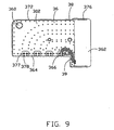
- FIGS. 8 and 9 show opposite faces of the circuit board 36 that may be used in the connector 100.
- On a first face 300 of each circuit board 36 are alternating signal traces 370 and grounding traces 372, and on a second face 302 of each circuit board 36 are only the grounding traces 372.
- Each circuit board 36 has conductive pads on the mating portion 362 which are allocated as signal pads 374 and grounding pads 376.
- the signal pads 374 are electrically connected to the signal traces 370, and these pads 374 are all on the first face 300 of each circuit board 36.
- the grounding pads 376 are electrically connected to the grounding traces 372, and these pads 376 are disposed on the first face 300 and the second face 302 of each circuit board 36. Electrical connections between the grounding pads 376 on the opposite faces of the circuit board 36 are made by the grounding traces 372 through conductive vias 38.
- the signal traces 370 are coupled to have plural differential pairs on the first face 300. Adjacent differential pairs of the signal traces 370 are separated by the grounding traces 372.
- the signal traces 370 of the differential pair extend from corresponding signal pads 374 adjacent innermost edges 375, i.e., the signal traces 370 of the differential pair are very closely spaced to have a relatively large distance between adjacent differential pairs, thereby enhancing reduction of crosstalk between adjacent differential pairs.
- the lowest differential pair has traces 39 on the second face 302 to reduce length and make trace routing easier.
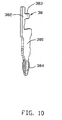
- the press-fit contacts 38 are secured to the mounting portion 364 of the circuit board 36 by surface mount soldering, which will be described in detail hereinafter.
- each press-fit contact 38 includes an intermediate portion 380 having an interference fit in a corresponding passageway 14 of the housing 1, a connecting portion 382 extending upwardly from an upper end of the intermediate portion 380 for surface mount soldering to the mounting portion 364 of the circuit board 36, and a compliant tail 384 extending downwardly from a lower end of the intermediate portion 380 for insertion into the plated through hole of the PCB.
- the connecting portion 382 is positioned adjacent a first side of the intermediate portion 380 and is formed with a projection 383 extending toward an opposite second side of the intermediate portion 380.
- each circuit board 36 defines an upper row of plated through holes 377 for receiving the projections 383 of the press-fit contacts 38 and a lower row of half plated through holes 378 in a bottom edge thereof and aligned with corresponding plated through holes 377 for partially receiving the upper ends of the intermediate portions 380 of the press-fit contacts 38.
- FIG. 4 shows the press-fit contacts 38 soldered to the mounting portion 364 of the circuit board 36.
- the first face 300 of the mounting portion 364 is coated with plural solder pastes 35 which are electrically connected to the corresponding signal and grounding traces 370, 372, respectively.
- the press-fit contacts 38 are placed on the solder pastes 35 with the projections 383 received in the plated through holes 377 and the upper ends of the intermediate portions 380 received in the half plated through holes 378. After the solder 35 is melt, interstitial space between the projection 383 of the press-fit contact 38 and the corresponding plated through hole 377 of the circuit board 36 is filled with the solder 35.
- interstitial space between the intermediate portion 380 and the corresponding half plated through hole 378 of the circuit board 36 is also filled with the solder 35. Therefore, when the melting solder 35 is cooled and solidified, the press-fit contacts 38 are reliably connected with the mounting portion 364 of the circuit board 36, e.g., there is redundant solder connection between the circuit board 36 and the press-fit contact 38 by use of plated through hole 377 and the half plated through hole 378, whereby the circuit board 36 can withstand the compliant insertion forces of the press-fit contacts 38.
- the shield member 2 in conjunction with the housing 1 obviate the need for a separate box or housing to hold the circuit board modules 3, thereby simplifying the connector 100. It can be understood that the employment of the shield member 2 and the circuit board modules 3 as described in the present invention enhances the electrical and the mechanical performance of the connector 100.
Abstract
Description
- The present invention relates to an electrical connector, and particularly to a high speed electrical connector having plural circuit board modules.
- With the development of communication and computer technology, high density electrical connectors with conductive elements in a matrix arrangement are desired to construct a large number of signal transmitting paths between two electronic devices. Such high density electrical connectors are widely used in internal connecting systems of severs, routers and the like requiring high speed data processing and communication.
- Due to continuing trends toward miniaturization and improved electrical performance by the electronics industry, requirements for greater contact density and higher electrical speeds are constantly being promulgated. This results in an increasing number of signals in the limited space of the connector. As the signal circuits are spaced closer and the transmission speed of the signals increases, electromagnetic inference (EMI) and the crosstalk become a serious problem.
- US-A-6171115 and 6267604 each disclose a high speed connector having plural individual circuit boards to reduce crosstalk. The connector comprises a front housing portion having a front wall with a plurality of parallel apertures extending therethrough, and an organizer attached to the front housing portion to retain the plural individual circuit boards therebetween. The organizer has a plurality of spaced slots located corresponding to the apertures, and a plurality of openings communicating with the slots in a bottom wall thereof. The circuit boards have mating portions extending through the apertures of the front housing portion for mating with a complementary connector, and mounting edges received in the slots of the organizer. The mounting edges of the circuit boards have a plurality of terminals secured thereon by soldering. The terminals extend through respective openings of the organizer for electrically connecting with a circuit substrate.
- US-A-6083047 and 6540558 each disclose a high speed connector having plural terminal modules retained to an insulating housing thereof. Each of the terminal modules comprises a dielectric cover and a printed circuit board (PCB) assembly associated with the dielectric cover. The PCB assembly includes an insulating substrate having a mating edge and a mounting edge perpendicular to each other, a plurality of circuit traces extending from the mating edge to the mounting edge, a plurality of socket terminals soldered to the mating edge for engaging with a complementary connector, and a plurality of press-fit terminals soldered to the mounting edge for connection to a printed circuit board on which the connector is mounted. Each press-fit terminal has a compliant tail which can be compressed upon insertion of the press-fit terminal into a corresponding through hole of the printed circuit board and then tends to restore to its original shape to engage surfaces within the through hole to thereby hold the connector on the printed circuit board. The press-fit terminal with a high retention force typically requires a high insertion force, which results in that the press-fit terminal is easy to deflect during the insertion of the press-fit terminal into the through hole of the circuit board. As a result, the connector is unreliably positioned on the printed circuit board and an electrical connection is adversely affected between the connector and the printed circuit board.
- On the other hand, there exists a common disadvantage in the above-mentioned patents that the electromagnetic interference are still not solved. The high speed electrical connector equipped with shielding to reduce EMI can be referred to US-A-5980321 (hereinafter the '321 patent). The connector disclosed in the '321 patent comprises a plurality of wafers side-by-side stacked and a metal stiffer holding the wafers in a required position. Each wafer is made in two pieces, a shield piece and a signal piece. The shield piece is formed by insert molding housing around a front portion thereof. The signal piece is made by insert molding housing around contacts. In order to hold each wafer in the required position without rotation, three connection points are established between the metal stiffer and the wafer. The connection comprises projections formed on the wafer and corresponding slots defined in the stiffer. However, the projections must be accurately aligned with corresponding slots, respectively, thereby complicating the manufacture of the connector as well as the assembly thereof. Further, the arrangement of positioning the shield pieces between the adjacent signal pieces reduces the effective signal density.
- Hence, an improved electrical connector is required to overcome the disadvantages of the related art.
- The present invention seeks to provide a high density electrical connector having enhanced electrical performance with a simplified configuration.
- The present invention seeks to provide a high density electrical connector having plural press-fit contacts which can reliably connect with a printed circuit board to which the connector is mounted.
- A high density electrical connector in accordance with the present invention comprises a unitary insulative housing defining a plurality of parallel slots, a plurality of parallelly arranged circuit board modules and a shield member attached to the housing. The circuit board modules are retained by and between the shield member and the housing. Each circuit board module includes a dielectric spacer, a circuit board attached to the dielectric spacer and received in a corresponding slot of the housing, and a row of contacts mechanically and electrically connecting with the circuit board and disposed in the corresponding slot.
- According to one aspect of the present invention, the circuit board has a mounting portion received in the slot and with a fusible element disposed thereon. The mounting portion defines a plurality of plated through holes therein. Each contact includes an intermediate portion, a connecting portion extending upwardly from the intermediate portion and surface mounted to the mounting portion, and a tail portion extending downwardly from the intermediate portion adapted for connecting with a printed circuit board. The connecting portion has a projection received in the plated through hole. Interstitial space between the plated through hole and the projection is substantially filled with fusible element after melting and solidifying the fusible element.
- Other advantages and novel features of the invention will become more apparent from the following detailed description when taken in conjunction with the accompanying drawings.
- FIG. 1 is an assembled perspective view of an electrical connector in accordance with the present invention;
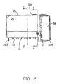
- FIG. 2 is a side elevation view of the electrical connector shown in FIG. 1;
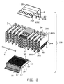
- FIG. 3 is an exploded perspective view of the connector shown in FIG. 1;
- FIG. 4 is an enlarged view of a circled portion A of FIG. 3;
- FIG. 5 is an exploded perspective view of a circuit board module used in the connector with press-fit contacts being omitted;
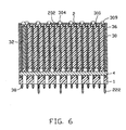
- FIG. 6 is a cross-section view of the connector taken along line 6-6 of FIG 2;
- FIG. 7 is a cross-section view of the connector taken along line 7-7 of FIG. 2;
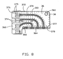
- FIG. 8 is a first side elevation view of a circuit board that may be used in the connector;
- FIG. 9 is a second side elevation view of the circuit board; and
- FIG. 10 is a perspective view of a contact used in the connector.
-
- Reference will now be made in detail to the preferred embodiment of the present invention.
- Referring to FIGS. 1, 2 and 3, an
electrical connector 100 in accordance with the present invention comprises a unitaryinsulating housing 1, ashield member 2, a plurality of individualcircuit board modules 3 received in thehousing 1, and analignment pin 4 inserting through thecircuit board modules 3. Theshield member 2 substantially encloses thehousing 1 and thecircuit board modules 3 for electromagnetic interference (EMI) protection. - The
housing 1 includes arectangular body 10 and a front tongue 11 extending forwardly from a lower portion of a front end of thebody 10. Thebody 10 defines a plurality ofparallel slots 13 extending along a longitudinal direction of thehousing 1, and plural rows ofpassageways 14 communicating withcorresponding slots 13 and penetrating through a bottom thereof. The tongue 11 defines a plurality ofgrooves 15 aligned withcorresponding slots 13. Thehousing 2 defines a row ofholes 16 at a rear end thereof and abore 17 laterally extending therethrough. - The
shield member 2 is stamped from a metal sheet and comprises atop plate 20 and arear plate 22 extending downwardly from a rear edge of thetop plate 20. Thetop plate 20 defines a plurality ofslots 202 adjacent a front edge thereof. Therear plate 22 is formed with a plurality offastening tabs 220 extending forwardly from a bottom edge thereof for being retained in corresponding recesses (not shown) of thehousing 1 and a plurality ofpositioning fingers 222 extending downwardly fromcorresponding tabs 220 for insertion into corresponding through holes of a printed circuit board (PCB) to which theconnector 100 is mounted for positioning theconnector 100 on the PCB. - The individual
circuit board modules 3 are side-by-side stacked. In a preferred embodiment, each one of thecircuit board modules 3 is substantially identical in structure except for a left outermost one of FIG. 3. As best shown in FIG. 5, the left outermostcircuit board module 3 comprises adielectric spacer 30, adielectric block 32 and acircuit board assembly 34 securely sandwiched between thedielectric spacer 30 and thedielectric block 32. Thedielectric spacer 30 is a flat plate and defines arecess 300 in a first side thereof receiving thecircuit board assembly 34. Thedielectric spacer 30 includes a plurality of laterally extendingposts 302 in therecess 300, a T-shaped protrusion 304 on a top edge thereof, atab 306 with an opening 307 defined therein extending downwardly from a bottom edge adjacent a front end thereof, and apositioning pin 308 extending downwardly from the bottom edge adjacent a rear end thereof. Thecircuit board assembly 34 includes acircuit board 36 and a plurality of press-fit contacts 38 (shown in FIG 3) electrically and mechanically connecting with thecircuit board 36. Thecircuit board 36 defines a corresponding number ofretention holes 360 receiving theposts 302 of thedielectric spacer 30 to thereby secure thecircuit board assembly 34 with thedielectric spacer 30. Thedielectric block 32 defines a corresponding number of throughholes 320 receiving theposts 302 of thedielectric spacer 30 to thereby sandwich thecircuit board assembly 34 between thedielectric spacer 30 and thedielectric block 32. - Referring again to FIG. 3, each of the other
circuit board modules 3 has a structure substantially the same as the left outermost one except that thedielectric block 32 is not introduced and therecess 300 is defined in a second opposite side of thedielectric spacer 30. Every two adjacentcircuit board modules 3 are side to side stackable with use of extended posts 309 (only one is shown) on one of the two adjacentdielectric spacers 30 and recessedholes 310 in another of the two adjacentdielectric spacers 30. - The
circuit board 36 has amating portion 362 extending beyond the front edge of thedielectric spacer 30 and a mountingportion 364 extending beyond the bottom edge of thedielectric spacer 30. Thecircuit board 36 includes a dielectric substrate made of conventional circuit board substrate material, such as FR4, and signal and grounding traces on the substrate. The signal and the grounding traces of thecircuit board 36 provide electrical paths from themating portion 362 to the mountingportion 364. Each of thecircuit boards 36 defines a throughhole 366 aligned with thebore 17 of thehousing 1 and theopening 307 of thedielectric spacer 30. It is noted that the T-shapedprotrusion 304 may be formed on every otherdielectric spacer 30 rather than on eachdielectric spacer 30. - Referring to FIGS. 6 and 7 in conjunction with FIG. 3, the
circuit board modules 3 are first installed in theshield member 2 with theprotrusions 304 received in correspondingslots 202 and then are assembled to thehousing 1 by locating the positioning pins 308 in theholes 16 and inserting the mountingportions 364 into theslots 13. The press-fit contacts 38 are received in thepassageways 14 of thehousing 1 and extend beyond the bottom of thehousing 1 for being press-fitted into corresponding plated through holes of the PCB. Thecircuit boards 36 have front,lower edges 365 received in thegrooves 15 of thehousing 1. After thecircuit board modules 3 are assembled to thehousing 1, thealignment pin 4 inserts through thebore 17 of thehousing 1, theopenings 307 of thedielectric spacers 30 and the throughholes 366 of thecircuit boards 36, thereby providing an accurate position of themating portions 362 of thecircuit boards 36. - FIGS. 8 and 9 show opposite faces of the
circuit board 36 that may be used in theconnector 100. On afirst face 300 of eachcircuit board 36 are alternating signal traces 370 and grounding traces 372, and on asecond face 302 of eachcircuit board 36 are only the grounding traces 372. - Each
circuit board 36 has conductive pads on themating portion 362 which are allocated assignal pads 374 andgrounding pads 376. Thesignal pads 374 are electrically connected to the signal traces 370, and thesepads 374 are all on thefirst face 300 of eachcircuit board 36. Thegrounding pads 376 are electrically connected to the grounding traces 372, and thesepads 376 are disposed on thefirst face 300 and thesecond face 302 of eachcircuit board 36. Electrical connections between the groundingpads 376 on the opposite faces of thecircuit board 36 are made by the grounding traces 372 throughconductive vias 38. - The signal traces 370 are coupled to have plural differential pairs on the
first face 300. Adjacent differential pairs of the signal traces 370 are separated by the grounding traces 372. The signal traces 370 of the differential pair extend fromcorresponding signal pads 374 adjacentinnermost edges 375, i.e., the signal traces 370 of the differential pair are very closely spaced to have a relatively large distance between adjacent differential pairs, thereby enhancing reduction of crosstalk between adjacent differential pairs. The lowest differential pair has traces 39 on thesecond face 302 to reduce length and make trace routing easier. - According to one aspect of the invention as shown in FIGS. 3 and 4, the press-
fit contacts 38 are secured to the mountingportion 364 of thecircuit board 36 by surface mount soldering, which will be described in detail hereinafter. - Referring to FIG. 10 in conjunction with FIG. 7, each press-
fit contact 38 includes anintermediate portion 380 having an interference fit in a correspondingpassageway 14 of thehousing 1, a connectingportion 382 extending upwardly from an upper end of theintermediate portion 380 for surface mount soldering to the mountingportion 364 of thecircuit board 36, and acompliant tail 384 extending downwardly from a lower end of theintermediate portion 380 for insertion into the plated through hole of the PCB. The connectingportion 382 is positioned adjacent a first side of theintermediate portion 380 and is formed with aprojection 383 extending toward an opposite second side of theintermediate portion 380. - Referring back to FIGS. 8 and 9, according to the invention, the mounting
portion 364 of eachcircuit board 36 defines an upper row of plated throughholes 377 for receiving theprojections 383 of the press-fit contacts 38 and a lower row of half plated throughholes 378 in a bottom edge thereof and aligned with corresponding plated throughholes 377 for partially receiving the upper ends of theintermediate portions 380 of the press-fit contacts 38. - FIG. 4 shows the press-
fit contacts 38 soldered to the mountingportion 364 of thecircuit board 36. Thefirst face 300 of the mountingportion 364 is coated with plural solder pastes 35 which are electrically connected to the corresponding signal and grounding traces 370, 372, respectively. The press-fit contacts 38 are placed on the solder pastes 35 with theprojections 383 received in the plated throughholes 377 and the upper ends of theintermediate portions 380 received in the half plated throughholes 378. After thesolder 35 is melt, interstitial space between theprojection 383 of the press-fit contact 38 and the corresponding plated throughhole 377 of thecircuit board 36 is filled with thesolder 35. In addition, interstitial space between theintermediate portion 380 and the corresponding half plated throughhole 378 of thecircuit board 36 is also filled with thesolder 35. Therefore, when themelting solder 35 is cooled and solidified, the press-fit contacts 38 are reliably connected with the mountingportion 364 of thecircuit board 36, e.g., there is redundant solder connection between thecircuit board 36 and the press-fit contact 38 by use of plated throughhole 377 and the half plated throughhole 378, whereby thecircuit board 36 can withstand the compliant insertion forces of the press-fit contacts 38. - It is noted that the
shield member 2 in conjunction with thehousing 1 obviate the need for a separate box or housing to hold thecircuit board modules 3, thereby simplifying theconnector 100. It can be understood that the employment of theshield member 2 and thecircuit board modules 3 as described in the present invention enhances the electrical and the mechanical performance of theconnector 100. - It is to be understood, however, that even though numerous characteristics and advantages of the present invention have been set forth in the foregoing description, together with details of the structure and function of the invention, the disclosure is illustrative only, and changes may be made in detail, especially in matters of shape, size, and arrangement of parts within the principles of the invention to the full extent indicated by the broad general meaning of the terms in which the appended claims are expressed.
Claims (20)
- An electrical connector comprising:a unitary insulative housing defining a plurality of parallel slots;a plurality of parallelly arranged circuit board modules each comprising a dielectric spacer, a circuit board attached to the dielectric spacer and received in a corresponding slot of the housing, and a row of contacts mechanically and electrically connecting with the circuit board and disposed in the corresponding slot; anda shield member attached to the housing, the circuit board modules being retained by and between the shield member and the housing.
- An electrical connector as claimed in claim 1, wherein the shield member defines a plurality of slots in a top wall thereof, and the dielectric spacers comprise a plurality of protrusions received in the slots to retain upper portions of the circuit board modules.
- An electrical connector as claimed in claim 1 or 2, wherein the housing is vertically spaced from the top wall of the shield member and retains lower portions of the circuit board modules.
- An electrical connector as claimed in claim 3, wherein the housing defines a plurality of passageways at opposite sides of each slot and extending through a bottom thereof, and the contacts are soldered to the lower portions of the corresponding circuit boards and extend beyond a bottom of the housing through the passageways.
- An electrical connector as claimed in any preceding claim, wherein every two adjacent circuit board modules are side to side stackable with use of an extended post on one of the two adjacent dielectric spacers and a recessed hole in another of the two adjacent dielectric spacers.
- An electrical connector as claimed in any preceding claim, wherein the dielectric spacer of each circuit board module includes a recess and a plurality of laterally extending posts in the recess, and the circuit board is received in the recess of the dielectric spacer and defines a corresponding number of holes receiving the posts.
- An electrical connector as claimed in any preceding claim, wherein the shield member is formed with positioning fingers for insertion into corresponding through holes of a printed circuit board.
- An electrical connector as claimed in claim 7, wherein the shield member comprises a top plate covering a top of the parallel arranged circuit board modules and a rear plate covering a rear of the housing and the circuit board modules, the positioning fingers extending downwardly from the rear plate.
- An electrical connector as claimed in any preceding claim, wherein opposite outermost circuit board modules are arranged in such a manner that the dielectric spacers are located at outermost positions.
- An electrical connector as claimed in any preceding claim, wherein the housing comprises a front tongue at a lower portion of one end thereof, the front tongue defining a plurality of grooves aligned with corresponding slots, and wherein the circuit boards have mating portions with lower edges received in corresponding grooves.
- An electrical connector as claimed in any preceding claim, wherein the housing defines a row of holes adjacent a rear end thereof, and the dielectric spacers of the circuit board modules comprise a plurality of downwardly extending pins received in the holes.
- An electrical connector as claimed in any preceding claim, further comprising an alignment pin, and wherein each of the circuit boards defines a through hole, and each of the dielectric spacers defines an opening aligned with the through hole, the alignment pin inserting through the housing, the through holes of the circuit boards and the openings of the dielectric spacers.
- An electrical connector as claimed in any preceding claim, wherein the circuit board is located under the post of the corresponding spacer of the same circuit board modules.
- A circuit board assembly for using in an electrical connector for high speed signal transmission, comprising:a circuit board comprising a mating portion adapted for engaging with a complementary element, a mounting portion with a fusible element disposed thereon and defining a plated through hole therein; anda contact including an intermediate portion, a connecting portion extending upwardly from the intermediate portion and surface mounted to the mounting portion, and a tail portion extending downwardly from the intermediate portion adapted for connecting with a printed circuit board, the connecting portion having a projection received in the plated through hole, interstitial space between the plated through hole and the projection being substantially filled with fusible element after melting and solidifying the fusible element.
- A circuit board assembly as claimed in claim 14, wherein the connecting portion extends adjacent a first side of the intermediate portion, and the projection extends toward an opposite second side of the intermediate portion.
- A circuit board assembly as claimed in claim 14 or 15, wherein the mounting portion defines a half plated through hole at a bottom thereof and aligned with the plated through hole, and the intermediate portion has an upper end received in the half plated through hole, interstitial space between the half plated through hole and the upper end of the intermediate portion being substantially filled with fusible element after melting and solidifying the fusible element.
- A circuit board assembly comprising:a circuit board including a mounting area defining a surface thereon and a through hole therein;a contact including an intermediate portion, a connection portion extending from the intermediate portion in a first direction parallel to the surface and also engages the surface, a tail portion extending from the intermediate portion in a second direction away from said mounting area, and a projection extending from said connection portion in a third direction perpendicular to said surface and soldered within said through hole.
- A circuit board assembly as claimed in claim 17, wherein said intermediate portion abuts against an edge of said circuit board in said first direction.
- A circuit board assembly as claimed in claim 17 or 18, wherein said contact extends in a plane which is perpendicular to said surface.
- A circuit board assembly as claimed in claim 17, 18 or 19, wherein said second direction is opposite to said first direction.
Applications Claiming Priority (2)
| Application Number | Priority Date | Filing Date | Title |
|---|---|---|---|
| US10/728,536 US6875031B1 (en) | 2003-12-05 | 2003-12-05 | Electrical connector with circuit board module |
| US728536 | 2003-12-05 |
Publications (2)
| Publication Number | Publication Date |
|---|---|
| EP1538716A2 true EP1538716A2 (en) | 2005-06-08 |
| EP1538716A3 EP1538716A3 (en) | 2006-03-22 |
Family
ID=34377723
Family Applications (1)
| Application Number | Title | Priority Date | Filing Date |
|---|---|---|---|
| EP04255418A Withdrawn EP1538716A3 (en) | 2003-12-05 | 2004-09-07 | Electrical connector with circuit board module |
Country Status (5)
| Country | Link |
|---|---|
| US (1) | US6875031B1 (en) |
| EP (1) | EP1538716A3 (en) |
| JP (1) | JP2005174904A (en) |
| CN (1) | CN2749079Y (en) |
| TW (1) | TW200520325A (en) |
Cited By (2)
| Publication number | Priority date | Publication date | Assignee | Title |
|---|---|---|---|---|
| EP2667454A1 (en) | 2012-05-25 | 2013-11-27 | Weetech GmbH | Variable plug connector |
| WO2014084293A1 (en) * | 2012-11-30 | 2014-06-05 | 宏致日本株式会社 | Connector |
Families Citing this family (54)
| Publication number | Priority date | Publication date | Assignee | Title |
|---|---|---|---|---|
| FR2854302B1 (en) * | 2003-04-24 | 2005-07-22 | Arnould App Electr | WIRING CONCENTRATOR, SIGNAL DISTRIBUTION UNIT COMPRISING IT AND KIT COMPRISING SUCH UNIT |
| US7175445B2 (en) * | 2004-08-31 | 2007-02-13 | Tyco Electronics Corporation | Electrical connector power wafers |
| CN101164204B (en) * | 2005-02-22 | 2012-06-27 | 莫莱克斯公司 | Differential signal connector with wafer-style construction |
| US20090291593A1 (en) | 2005-06-30 | 2009-11-26 | Prescott Atkinson | High frequency broadside-coupled electrical connector |
| US7163421B1 (en) * | 2005-06-30 | 2007-01-16 | Amphenol Corporation | High speed high density electrical connector |
| US7270574B1 (en) * | 2006-02-07 | 2007-09-18 | Fci Americas Technology, Inc. | Covers for electrical connectors |
| US7175479B1 (en) * | 2006-04-25 | 2007-02-13 | Tyco Electronics Corporation | Modular connector assembly with stamped retention latch members |
| US7794240B2 (en) * | 2007-04-04 | 2010-09-14 | Amphenol Corporation | Electrical connector with complementary conductive elements |
| US7722401B2 (en) | 2007-04-04 | 2010-05-25 | Amphenol Corporation | Differential electrical connector with skew control |
| US7794278B2 (en) * | 2007-04-04 | 2010-09-14 | Amphenol Corporation | Electrical connector lead frame |
| JP5019174B2 (en) * | 2007-08-03 | 2012-09-05 | 山一電機株式会社 | High-speed transmission connector |
| US7390194B1 (en) * | 2007-09-17 | 2008-06-24 | International Business Machines Corporation | High speed mezzanine connector |
| JP4862796B2 (en) * | 2007-09-28 | 2012-01-25 | 山一電機株式会社 | High-density connector for high-speed transmission |
| US20090163047A1 (en) * | 2007-12-24 | 2009-06-25 | Myoungsoo Jeon | Connector having both press-fit pins and high-speed conductive resilient surface contact elements |
| US7727000B2 (en) * | 2008-01-02 | 2010-06-01 | Fci Americas Technology, Inc. | Electrical connector having guidance for mating |
| US8469720B2 (en) | 2008-01-17 | 2013-06-25 | Amphenol Corporation | Electrical connector assembly |
| CN201204312Y (en) * | 2008-03-25 | 2009-03-04 | 富士康(昆山)电脑接插件有限公司 | Electric connector |
| JP4565031B2 (en) * | 2008-09-17 | 2010-10-20 | 山一電機株式会社 | High-speed transmission connector, high-speed transmission connector plug, and high-speed transmission connector socket |
| US7731533B2 (en) * | 2008-10-30 | 2010-06-08 | Tyco Electronics Corporation | Connector system having a vibration dampening shell |
| DE102009015462B4 (en) * | 2008-11-10 | 2014-10-30 | Erni Production Gmbh & Co. Kg | Angle connector with a shield and method of making the shield of the angle connector |
| CN102356517B (en) | 2009-02-04 | 2014-08-13 | 安费诺有限公司 | Differential electrical connector with improved skew control |
| US8550861B2 (en) | 2009-09-09 | 2013-10-08 | Amphenol TCS | Compressive contact for high speed electrical connector |
| WO2011140438A2 (en) | 2010-05-07 | 2011-11-10 | Amphenol Corporation | High performance cable connector |
| WO2012106554A2 (en) | 2011-02-02 | 2012-08-09 | Amphenol Corporation | Mezzanine connector |
| WO2014031851A1 (en) | 2012-08-22 | 2014-02-27 | Amphenol Corporation | High-frequency electrical connector |
| WO2014103566A1 (en) * | 2012-12-26 | 2014-07-03 | ソニー株式会社 | Connector, data receiving apparatus, data transmitting apparatus, and data transmitting/receiving system |
| US10164380B2 (en) | 2013-02-27 | 2018-12-25 | Molex, Llc | Compact connector system |
| JP5843829B2 (en) * | 2013-09-17 | 2016-01-13 | ヒロセ電機株式会社 | Relay electrical connector |
| CN106104933B (en) | 2014-01-22 | 2020-09-11 | 安费诺有限公司 | High speed, high density electrical connector with shielded signal paths |
| CN106415944A (en) | 2014-04-23 | 2017-02-15 | 泰科电子公司 | Electrical connector with shield cap and shielded terminals |
| WO2015196994A1 (en) * | 2014-06-27 | 2015-12-30 | 深圳市得润电子股份有限公司 | Cable connector, board end connector and combination thereof |
| CN108701922B (en) | 2015-07-07 | 2020-02-14 | Afci亚洲私人有限公司 | Electrical connector |
| CN106252968B (en) | 2016-07-29 | 2019-06-07 | 中航光电科技股份有限公司 | Electric connector |
| CN109863650B (en) | 2016-08-23 | 2020-10-02 | 安费诺有限公司 | Configurable high performance connector |
| US9923309B1 (en) * | 2017-01-27 | 2018-03-20 | Te Connectivity Corporation | PCB connector footprint |
| US10109959B1 (en) | 2017-05-25 | 2018-10-23 | Juniper Networks, Inc. | Electrical connector with embedded processor |
| US9997868B1 (en) * | 2017-07-24 | 2018-06-12 | Te Connectivity Corporation | Electrical connector with improved impedance characteristics |
| US11710917B2 (en) | 2017-10-30 | 2023-07-25 | Amphenol Fci Asia Pte. Ltd. | Low crosstalk card edge connector |
| CN208862209U (en) | 2018-09-26 | 2019-05-14 | 安费诺东亚电子科技(深圳)有限公司 | A kind of connector and its pcb board of application |
| WO2020073460A1 (en) | 2018-10-09 | 2020-04-16 | Amphenol Commercial Products (Chengdu) Co. Ltd. | High-density edge connector |
| US10506737B1 (en) * | 2018-12-17 | 2019-12-10 | Te Connectivity Corporation | Airflow fairings for circuit card assemblies of a communication system |
| TWM582251U (en) | 2019-04-22 | 2019-08-11 | 香港商安費諾(東亞)有限公司 | Connector set with hidden locking mechanism and socket connector thereof |
| CN110620300A (en) * | 2019-05-21 | 2019-12-27 | 中航光电科技股份有限公司 | Connector fixing piece and connector |
| TW202127754A (en) | 2019-11-06 | 2021-07-16 | 香港商安費諾(東亞)有限公司 | High-frequency electrical connector with interlocking segments |
| US11588277B2 (en) | 2019-11-06 | 2023-02-21 | Amphenol East Asia Ltd. | High-frequency electrical connector with lossy member |
| CN113131236B (en) * | 2019-12-31 | 2023-05-16 | 富鼎精密工业(郑州)有限公司 | Electric connector |
| CN113131259B (en) * | 2019-12-31 | 2023-08-15 | 富鼎精密工业(郑州)有限公司 | Electric connector |
| US11469554B2 (en) | 2020-01-27 | 2022-10-11 | Fci Usa Llc | High speed, high density direct mate orthogonal connector |
| TW202135385A (en) | 2020-01-27 | 2021-09-16 | 美商Fci美國有限責任公司 | High speed connector |
| US11264749B2 (en) * | 2020-03-26 | 2022-03-01 | TE Connectivity Services Gmbh | Modular connector with printed circuit board wafer to reduce crosstalk |
| US11652307B2 (en) | 2020-08-20 | 2023-05-16 | Amphenol East Asia Electronic Technology (Shenzhen) Co., Ltd. | High speed connector |
| CN212874843U (en) | 2020-08-31 | 2021-04-02 | 安费诺商用电子产品(成都)有限公司 | Electrical connector |
| CN215816516U (en) | 2020-09-22 | 2022-02-11 | 安费诺商用电子产品(成都)有限公司 | Electrical connector |
| CN213636403U (en) | 2020-09-25 | 2021-07-06 | 安费诺商用电子产品(成都)有限公司 | Electrical connector |
Citations (4)
| Publication number | Priority date | Publication date | Assignee | Title |
|---|---|---|---|---|
| EP1107369A1 (en) * | 1999-12-03 | 2001-06-13 | F.C.I. - Framatome Connectors International | Shielded connector assembly |
| US20020111068A1 (en) * | 1997-02-07 | 2002-08-15 | Cohen Thomas S. | Printed circuit board for differential signal electrical connectors |
| WO2002065589A1 (en) * | 2001-02-12 | 2002-08-22 | Perlos Oyj | Connector and contact wafer |
| US20020137373A1 (en) * | 2000-12-21 | 2002-09-26 | Billman Timothy B. | Electrical connector having improved grounding terminals |
Family Cites Families (7)
| Publication number | Priority date | Publication date | Assignee | Title |
|---|---|---|---|---|
| US6083047A (en) | 1997-01-16 | 2000-07-04 | Berg Technology, Inc. | Modular electrical PCB assembly connector |
| US5980321A (en) | 1997-02-07 | 1999-11-09 | Teradyne, Inc. | High speed, high density electrical connector |
| US6267604B1 (en) | 2000-02-03 | 2001-07-31 | Tyco Electronics Corporation | Electrical connector including a housing that holds parallel circuit boards |
| US6171115B1 (en) | 2000-02-03 | 2001-01-09 | Tyco Electronics Corporation | Electrical connector having circuit boards and keying for different types of circuit boards |
| US6709298B2 (en) * | 2001-04-06 | 2004-03-23 | Litton Systems, Inc. | Insulator coring and contact configuration to prevent pin stubbing in the throat of tuning fork socket connector contacts |
| US6655966B2 (en) * | 2002-03-19 | 2003-12-02 | Tyco Electronics Corporation | Modular connector with grounding interconnect |
| US6638079B1 (en) * | 2002-05-21 | 2003-10-28 | Hon Hai Precision Ind. Co., Ltd. | Customizable electrical connector |
-
2003
- 2003-12-05 US US10/728,536 patent/US6875031B1/en not_active Expired - Fee Related
-
2004
- 2004-08-13 JP JP2004236057A patent/JP2005174904A/en not_active Withdrawn
- 2004-08-20 TW TW093125096A patent/TW200520325A/en unknown
- 2004-09-07 EP EP04255418A patent/EP1538716A3/en not_active Withdrawn
- 2004-10-27 CN CNU2004201150474U patent/CN2749079Y/en not_active Expired - Fee Related
Patent Citations (4)
| Publication number | Priority date | Publication date | Assignee | Title |
|---|---|---|---|---|
| US20020111068A1 (en) * | 1997-02-07 | 2002-08-15 | Cohen Thomas S. | Printed circuit board for differential signal electrical connectors |
| EP1107369A1 (en) * | 1999-12-03 | 2001-06-13 | F.C.I. - Framatome Connectors International | Shielded connector assembly |
| US20020137373A1 (en) * | 2000-12-21 | 2002-09-26 | Billman Timothy B. | Electrical connector having improved grounding terminals |
| WO2002065589A1 (en) * | 2001-02-12 | 2002-08-22 | Perlos Oyj | Connector and contact wafer |
Cited By (5)
| Publication number | Priority date | Publication date | Assignee | Title |
|---|---|---|---|---|
| EP2667454A1 (en) | 2012-05-25 | 2013-11-27 | Weetech GmbH | Variable plug connector |
| DE102012104549A1 (en) * | 2012-05-25 | 2013-11-28 | Weetech Gmbh | Variable connector of a connector |
| US9065193B2 (en) | 2012-05-25 | 2015-06-23 | Weetech Gmbh | Variable plug of a connector |
| DE102012104549B4 (en) * | 2012-05-25 | 2016-07-28 | Weetech Gmbh | Variable connector of a connector |
| WO2014084293A1 (en) * | 2012-11-30 | 2014-06-05 | 宏致日本株式会社 | Connector |
Also Published As
| Publication number | Publication date |
|---|---|
| TW200520325A (en) | 2005-06-16 |
| CN2749079Y (en) | 2005-12-28 |
| US6875031B1 (en) | 2005-04-05 |
| EP1538716A3 (en) | 2006-03-22 |
| JP2005174904A (en) | 2005-06-30 |
Similar Documents
| Publication | Publication Date | Title |
|---|---|---|
| US6875031B1 (en) | Electrical connector with circuit board module | |
| US6884117B2 (en) | Electrical connector having circuit board modules positioned between metal stiffener and a housing | |
| US6808419B1 (en) | Electrical connector having enhanced electrical performance | |
| US11742620B2 (en) | High-frequency electrical connector | |
| US6641438B1 (en) | High speed, high density backplane connector | |
| JP2949449B2 (en) | Shielded electrical connector | |
| US6592407B2 (en) | High-speed card edge connector | |
| US6551140B2 (en) | Electrical connector having differential pair terminals with equal length | |
| US7494379B2 (en) | Connector with reference conductor contact | |
| US5135405A (en) | Connectors with ground structure | |
| US5664968A (en) | Connector assembly with shielded modules | |
| US6102747A (en) | Modular connectors | |
| EP0854549B1 (en) | Surface mount connector with integrated PCB assembly | |
| US7086901B2 (en) | Shielded electrical connector | |
| US6623310B1 (en) | High density electrical connector assembly with reduced insertion force | |
| US5228864A (en) | Connectors with ground structure | |
| TWI505569B (en) | High density connector assembly | |
| US4976628A (en) | Modules for cable assemblies | |
| US6814612B1 (en) | Shielded electrical connector | |
| US7736176B2 (en) | Modular jack assembly having improved connecting terminal | |
| US6739915B1 (en) | Electrical connector with rear retention mechanism of outer shell | |
| US6648689B1 (en) | High density electrical connector having enhanced crosstalk reduction capability | |
| US20060228911A1 (en) | Connector assembly for printed circuit board interconnection | |
| US6682369B1 (en) | Electrical connector having retention system for precisely mounting plural boards therein | |
| US6645009B1 (en) | High density electrical connector with lead-in device |
Legal Events
| Date | Code | Title | Description |
|---|---|---|---|
| PUAI | Public reference made under article 153(3) epc to a published international application that has entered the european phase |
Free format text: ORIGINAL CODE: 0009012 |
|
| AK | Designated contracting states |
Kind code of ref document: A2 Designated state(s): AT BE BG CH CY CZ DE DK EE ES FI FR GB GR HU IE IT LI LU MC NL PL PT RO SE SI SK TR |
|
| AX | Request for extension of the european patent |
Extension state: AL HR LT LV MK |
|
| PUAL | Search report despatched |
Free format text: ORIGINAL CODE: 0009013 |
|
| AK | Designated contracting states |
Kind code of ref document: A3 Designated state(s): AT BE BG CH CY CZ DE DK EE ES FI FR GB GR HU IE IT LI LU MC NL PL PT RO SE SI SK TR |
|
| AX | Request for extension of the european patent |
Extension state: AL HR LT LV MK |
|
| 17P | Request for examination filed |
Effective date: 20060630 |
|
| AKX | Designation fees paid |
Designated state(s): AT BE BG CH CY CZ DE DK EE ES FI FR GB GR HU IE IT LI LU MC NL PL PT RO SE SI SK TR |
|
| AXX | Extension fees paid |
Extension state: LV Payment date: 20060729 Extension state: LT Payment date: 20060729 |
|
| STAA | Information on the status of an ep patent application or granted ep patent |
Free format text: STATUS: THE APPLICATION IS DEEMED TO BE WITHDRAWN |
|
| 18D | Application deemed to be withdrawn |
Effective date: 20110401 |