EP1630871B1 - Imaging device and imaging method - Google Patents
Imaging device and imaging method Download PDFInfo
- Publication number
- EP1630871B1 EP1630871B1 EP04728931A EP04728931A EP1630871B1 EP 1630871 B1 EP1630871 B1 EP 1630871B1 EP 04728931 A EP04728931 A EP 04728931A EP 04728931 A EP04728931 A EP 04728931A EP 1630871 B1 EP1630871 B1 EP 1630871B1
- Authority
- EP
- European Patent Office
- Prior art keywords
- near infrared
- visible light
- infrared light
- components
- pixels
- Prior art date
- Legal status (The legal status is an assumption and is not a legal conclusion. Google has not performed a legal analysis and makes no representation as to the accuracy of the status listed.)
- Active
Links
- 238000003384 imaging method Methods 0.000 title claims abstract description 69
- 238000001514 detection method Methods 0.000 claims abstract description 68
- 230000003287 optical effect Effects 0.000 claims abstract description 29
- 239000004065 semiconductor Substances 0.000 claims description 30
- 238000000034 method Methods 0.000 claims description 5
- 230000031700 light absorption Effects 0.000 claims description 4
- 239000003086 colorant Substances 0.000 description 16
- 239000000758 substrate Substances 0.000 description 8
- XUIMIQQOPSSXEZ-UHFFFAOYSA-N Silicon Chemical compound [Si] XUIMIQQOPSSXEZ-UHFFFAOYSA-N 0.000 description 4
- 238000012937 correction Methods 0.000 description 4
- 229910052710 silicon Inorganic materials 0.000 description 4
- 239000010703 silicon Substances 0.000 description 4
- 230000004048 modification Effects 0.000 description 3
- 238000012986 modification Methods 0.000 description 3
- 230000004075 alteration Effects 0.000 description 2
- 238000002835 absorbance Methods 0.000 description 1
- 230000008901 benefit Effects 0.000 description 1
- 230000015556 catabolic process Effects 0.000 description 1
- 239000002131 composite material Substances 0.000 description 1
- 238000006731 degradation reaction Methods 0.000 description 1
- 239000000203 mixture Substances 0.000 description 1
- 230000008569 process Effects 0.000 description 1
Images


Classifications
-
- H—ELECTRICITY
- H04—ELECTRIC COMMUNICATION TECHNIQUE
- H04N—PICTORIAL COMMUNICATION, e.g. TELEVISION
- H04N23/00—Cameras or camera modules comprising electronic image sensors; Control thereof
- H04N23/10—Cameras or camera modules comprising electronic image sensors; Control thereof for generating image signals from different wavelengths
- H04N23/11—Cameras or camera modules comprising electronic image sensors; Control thereof for generating image signals from different wavelengths for generating image signals from visible and infrared light wavelengths
-
- H—ELECTRICITY
- H01—ELECTRIC ELEMENTS
- H01L—SEMICONDUCTOR DEVICES NOT COVERED BY CLASS H10
- H01L27/00—Devices consisting of a plurality of semiconductor or other solid-state components formed in or on a common substrate
- H01L27/14—Devices consisting of a plurality of semiconductor or other solid-state components formed in or on a common substrate including semiconductor components sensitive to infrared radiation, light, electromagnetic radiation of shorter wavelength or corpuscular radiation and specially adapted either for the conversion of the energy of such radiation into electrical energy or for the control of electrical energy by such radiation
- H01L27/144—Devices controlled by radiation
- H01L27/146—Imager structures
- H01L27/14643—Photodiode arrays; MOS imagers
- H01L27/14645—Colour imagers
-
- H—ELECTRICITY
- H01—ELECTRIC ELEMENTS
- H01L—SEMICONDUCTOR DEVICES NOT COVERED BY CLASS H10
- H01L31/00—Semiconductor devices sensitive to infrared radiation, light, electromagnetic radiation of shorter wavelength or corpuscular radiation and specially adapted either for the conversion of the energy of such radiation into electrical energy or for the control of electrical energy by such radiation; Processes or apparatus specially adapted for the manufacture or treatment thereof or of parts thereof; Details thereof
- H01L31/08—Semiconductor devices sensitive to infrared radiation, light, electromagnetic radiation of shorter wavelength or corpuscular radiation and specially adapted either for the conversion of the energy of such radiation into electrical energy or for the control of electrical energy by such radiation; Processes or apparatus specially adapted for the manufacture or treatment thereof or of parts thereof; Details thereof in which radiation controls flow of current through the device, e.g. photoresistors
- H01L31/10—Semiconductor devices sensitive to infrared radiation, light, electromagnetic radiation of shorter wavelength or corpuscular radiation and specially adapted either for the conversion of the energy of such radiation into electrical energy or for the control of electrical energy by such radiation; Processes or apparatus specially adapted for the manufacture or treatment thereof or of parts thereof; Details thereof in which radiation controls flow of current through the device, e.g. photoresistors characterised by at least one potential-jump barrier or surface barrier, e.g. phototransistors
- H01L31/101—Devices sensitive to infrared, visible or ultraviolet radiation
-
- H—ELECTRICITY
- H04—ELECTRIC COMMUNICATION TECHNIQUE
- H04N—PICTORIAL COMMUNICATION, e.g. TELEVISION
- H04N25/00—Circuitry of solid-state image sensors [SSIS]; Control thereof
- H04N25/10—Circuitry of solid-state image sensors [SSIS]; Control thereof for transforming different wavelengths into image signals
- H04N25/11—Arrangement of colour filter arrays [CFA]; Filter mosaics
- H04N25/13—Arrangement of colour filter arrays [CFA]; Filter mosaics characterised by the spectral characteristics of the filter elements
- H04N25/131—Arrangement of colour filter arrays [CFA]; Filter mosaics characterised by the spectral characteristics of the filter elements including elements passing infrared wavelengths
-
- H—ELECTRICITY
- H04—ELECTRIC COMMUNICATION TECHNIQUE
- H04N—PICTORIAL COMMUNICATION, e.g. TELEVISION
- H04N25/00—Circuitry of solid-state image sensors [SSIS]; Control thereof
- H04N25/10—Circuitry of solid-state image sensors [SSIS]; Control thereof for transforming different wavelengths into image signals
- H04N25/17—Colour separation based on photon absorption depth, e.g. full colour resolution obtained simultaneously at each pixel location
-
- H—ELECTRICITY
- H04—ELECTRIC COMMUNICATION TECHNIQUE
- H04N—PICTORIAL COMMUNICATION, e.g. TELEVISION
- H04N2209/00—Details of colour television systems
- H04N2209/04—Picture signal generators
- H04N2209/041—Picture signal generators using solid-state devices
- H04N2209/042—Picture signal generators using solid-state devices having a single pick-up sensor
- H04N2209/047—Picture signal generators using solid-state devices having a single pick-up sensor using multispectral pick-up elements
Definitions
- the present invention relates to an imaging device and imaging method for detecting and receiving three components of visible light and near infrared light in different wavelength regions and for imaging pictures of both visible light and near infrared light.
- each of pixels can detect one of three colors of different wavelengths in visible light and near infrared light and such pixels are arranged in a mixed manner in the same imaging element, for example a CCD or CMOS imaging element (e.g. see Figure 2 of Japanese Patent Laid-Open Application No . 2002-142228 ).
- CCD or CMOS imaging element e.g. see Figure 2 of Japanese Patent Laid-Open Application No . 2002-142228 .
- Mg (magenta) color detectors 81, Ye (yellow) color detectors 82, Cy (cyan) color detectors 83, and near infrared light detectors 84 are arranged on an imaging element like a mosaic so that the combination repeats lengthwise and crosswise.
- one detector corresponds to just one pixel.
- a bare pixel has a property of detecting visible light and near infrared light of 400 nm to 1000 nm.
- an Mg color detector 81 is composed of a pixel covered with a bandpass filter for the region of the Mg color.
- the Ye color detectors 82 and Cy color detectors 83 are also composed of pixels covered with bandpass filters which derive the regions of their respective wavelengths. Bare pixels are arranged as the near infrared light detectors 84.
- the visible light region requires to be cut off. But it need not be cut off because obtaining luminance information will suffice.
- the above configuration allows imaging pictures of both visible light and near infrared light.
- three photodiodes are formed on a silicon substrate at different depths from the surface.
- This conventional device uses absorbance differences in silicon among three kinds of light of different wavelengths in the visible light region, e.g. blue, green, and red, to detect the three kinds of light of different wavelengths (e.g. see Figures 5 and 6 of Published Japanese Translation of PCT International Application ( Tokuhyo ) No. 2002-513145 ).
- three photodiodes of different depths can be arranged in one pixel.
- This prior art can therefore enable higher color resolution and prevent degradation of image quality caused by false color, in comparison with an art in which one pixel detects one color.
- Figure 11 shows the structure of a pixel formed on an imaging element.
- An n-type doped region 92 of an n-type semiconductor is formed on ap-type semiconductor substrate 91.
- ap-typedopedregion 93 is formed thereon.
- an n-type doped region 94 is formed thereon.
- a three-layer semiconductor structure triple-well structure
- blue light is absorbed at a depth of 0.2 ⁇ m in a silicon layer.
- Green is absorbed at 0.6 ⁇ m, and red is not absorbed until it reaches a depth of 2 ⁇ m. Accordingly, depths of interfaces, which work as photosensors for each light, are set to 0.2 ⁇ m, 0.6 ⁇ m, and 2 ⁇ m respectively. Three colors (three wavelength bands) of light can thus be taken out almost spectrally. Then, an electric current generated by blue light is detected by a current detector 95. Similarly, green light is detected by a current detector 96, and red light is detected by a current detector 97.
- an optical system comprising optical lenses commonly provides an image of a subject on the surface of an imaging element. Since focuses fundamentally differ depending on wavelengths, chromatic aberration occurs in imaged pictures (when one color comes into focus, the others go out of focus). So, as shown in Figure 12 , for example, an optical system having a property of an achromatic lens is commonly provided so that an imaging element is within the depth of focus (color shift is negligible within the range) with regard to magenta, yellow, and cyan in the visible light region, and the optical system therefore focuses.
- a purpose of the invention is to provide an excellent visible light and near infrared light imaging device and method which can obtain clear color images with good color reproducibility by a visible light detection means and can at the same time obtain clear luminance information or monochrome images by a near infrared light detection means.
- Imaging devices according to the invention are disclosed in claims 1 and 6. Imaging methods according to the present invention are disclosed in claims 9 and 10.
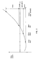
- a visible light and near infrared light imaging device related to the invention has an optical lens 1.
- the optical lens 1 is an optical system whose focal length is variable according to wavelengths, and makes three components of visible light and near infrared light in different wavelength regions form images at different locations according to their wavelengths.
- the optical lens 1 condenses light from an external subject and forms an image on an imaging element 2.
- light pencils from the optical lens 1 are shown separately by different wavelengths.
- the optical lens 1 forms images at different locations according to wavelengths as described above. This is shown more specifically in Figure 2 .
- the focal length of green of 520nm is 0.4 ⁇ m longer than the reference A.
- the focal length of red of 700nm is 2 ⁇ m longer than the reference A
- the focal length of near infrared of 1000nm is 10 ⁇ m longer than the reference A.
- the focal length of the optical lens 1 increases according to wavelengths, from that of short-wavelength light in visible light to near infrared light, and therefore three components of visible light and near infrared light form images at different locations.
- the imaging element 2 composes a light receiving section together with the optical lens 1 qua an optical system.
- Figure 3 schematically shows the configuration of the imaging element 2.
- visible light detection sections 6 and near infrared light detection sections 8 are arranged in the imaging element 2.
- the visible light detection section 6 comprises three detectors of different depths, and it detects with these three detectors three components of visible light in different wavelength regions which are condensed by the optical lens 1 and form images, using the fact that wavelength dependence of light absorption depth varies.
- the near infrared light detection section 8 has a detector which detects near infrared light.
- the visible light detection section 6 is composed of a blue detector 3, a green detector 4, and a red detector 5. These detectors 3 to 5 are photodiodes located at different depths from the surface. Three primary colors are obtained separately, so that any color is reproducible. Unlike the conventional Japanese Patent Laid-Open Application No. 2002-142228 , one pixel can obtain output of three colors in visible light. As described in explanations of conventional arts, it is actually impossible to separate light into three colors completely. But a degree of mixing of each color is known (or can be measured) in advance, so corrections can be made.
- the infrared light detection section 8 is composed of a near infrared light detector 7, which is a photodiode.
- the near infrared light detector 7 is located around the depth of the highest detectability.
- near infrared light is absorbed at a depth deeper than red light in a silicon layer. So, the near infrared light detector 7 is located, for example, at the depth of 10 ⁇ m.
- Luminance information can be obtained from the visible light detector 6 by combining three colors with one another. If output from the near infrared light detector 7 is to be in proportion to overall light intensity, output from the near infrared light detector 7 may be used as luminance information.
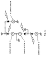
- Figure 4 shows the configuration of the imaging element 2 related to the first embodiment.
- the configuration of the visible light detection section 6 on the left of the figure is almost similar to the conventional example.
- An n-type doped region 10 of an n-type semiconductor is formed on a p-type semiconductor substrate 9.
- a p-type doped region 11 is formed thereon.
- an n-type doped region 12 is formed thereon.
- a three-layer semiconductor structure (triple-well structure) is made on the substrate.
- Three current detectors 14, 15, and 16 detect output of B, G, and R of visible light. But if the three colors are somewhat influenced by near infrared light, colors reproduced later may be different from real colors.
- a near infrared light cut filter 13 is placed in front of the light entrance to the current detectors. The influence of light in the near infrared region is thus eliminated.
- the near infrared light detection section 8 on the right of Figure 4 an n-type doped region 17 of an n-type semiconductor is formed additionally on the p-type semiconductor substrate 9.
- the current detector 18 detects a current when near infrared light comes in.
- the pn junction surface that is, the near infrared light detector 7 in Figure 3 , is provided at the depth of 10 ⁇ m. In this way, the near infrared light detector 7 is located where detectability for near infrared light is the highest.
- near infrared light has a very wide wavelength range from 770nm to 1000nm. Accordingly, the above-mentioned value may vary depending on the purpose of detection, i.e. which wavelength region is to be mainly detected.
- optical lens 1 described in Figures 1 and 2 , light in desired wavelength regions focuses on each detection area of the four current detectors 14, 15, 16, and 18. In other words, light of desired color comes into focus on a detection area of each detector. In order to realize this, the optical lens 1 is deliberately provided with aberration.
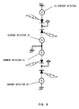
- Figure 5 shows an equivalent circuit schematic. As shown in Figure 5 , each photodiode is reversely biased, and currents corresponding to incoming light are detected. In the interests of simplicity, power supply and grounds are common in the equivalent circuit schematic of Figure 5 . However, the invention is not limited to this.
- Figures 6 and 7 show examples of actual arrangements of visible light detection sections 6 and near infrared light detection sections 8.
- visible light detection sections 6 and near infrared light detection sections 8 are arranged in a mixed manner.
- a visible light detector 30 composes the visible light detection section 6 and a near infrared light detector 31 composes the near infrared light detection section 8.
- the visible light detectors 30 and the near infrared light detectors 31 are alternately arranged in rows and columns in a mixed manner, and the ratio of the number or area of both pixels is one to one.
- visible light information in the area of the near infrared light detection section 8 an average for adjacent visible light detection sections 6 may be taken.
- resolution of color information may be lower than luminance resolution assuming that the use is humans' seeing images.
- this arrangement has higher resolution in both luminance and color than, for example, the conventional Japanese Patent Laid-Open Application No. 2002-142228 .
- Output from the near infrared light detection section 8 is useful as luminance information for detecting near infrared light in a relatively wide wavelength region.
- Sunlight especially contains a lot of near infrared light components.
- luminance information is obtained from adjacent near infrared light detection section 8.
- information from the near infrared light detection section 8 is used to correct output from the visible light detection section 6.
- luminance can usually be obtained by the following equation 1 when RGB is known.
- Y 0.299 ⁇ R + 0.587 ⁇ G + 0.114 ⁇ B
- luminance is a linear sum of RGB.
- luminance may be obtained by the following equation 2 when average luminance information I is derived from a plurality of adjacent near infrared light detection sections 8.
- Figure 7 shows a configuration in which luminance information from near infrared light is actively used.
- the S/N ratio and resolution of luminance information can be improved.
- the visible light detector 30 composes the visible light detection section 6
- the near infrared light detector 31 composes the near infrared light detection section 8.
- the visible light detectors 30 and the near infrared light detectors 31 are alternately arranged in rows and columns in a mixed manner.
- the ratio of the number or area of visible light detection sections 6 to that of near infrared light detection sections 8 is one to three in Figure 7 . More specifically, a set of one pixel of the visible light detection section 6 (visible light detector 30) and three pixels of the near infrared light detection sections (near infrared light detectors 31) is arranged in a square, and the sets are arranged in rows and columns. In this way, they are uniformly arranged in the ratio of one to three.
- luminance resolution rather than color resolution, can be improved. As a result, clear luminance information can be obtained for the range up to near infrared light.
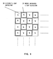
- Figure 8 shows a configuration of an imaging element related to a second embodiment
- Figure 9 is an equivalent circuit schematic of an imaging element related to the second embodiment.
- a visible light detection section and near infrared light detection section are placed in one pixel.
- the figure shows one pixel, which comprises a detection section to separate and detect three components of visible light and near infrared light in different wavelength regions, four components in total.
- four current detectors 23, 24, 25, and 26 arranged in one pixel detect B, G, and R of visible light and near infrared light.
- an n-type doped region 19 of an n-type semiconductor is formed on a p-type semiconductor substrate 9.
- a p-type doped region 20 is formed thereon.
- an n-type doped region 21 is formed thereon.
- a p-type doped region 22 is formed thereon.
- a four-layer semiconductor structure quaddruple-well structure
- each pn interface region functions as a photosensor, four photosensors can be made up in total.
- the depth of each interface i.e. detection area, is determined and controlled as previously described. Light in four wavelength regions of blue, green, red, and near infrared light can thus be detected. Actually, it is difficult to separate four colors of light completely, and a mixture occurs. But a degree of mixing of each color is known (or can be measured) in advance, so corrections can be made.
- Figure 9 is an equivalent circuit schematic of Figure 8 .
- Four photodiodes are reversely biased, and currents corresponding to incoming light are detected.
- power supply and grounds are common.
- the invention is not limited to this.
- the mixing of visible light into near infrared light is unavoidable.
- color reproducibility may be slightly worse in the second embodiment than in the first embodiment even if corrections are made.
- there is an advantage that resolution of both color and luminance is better because one pixel simultaneously processes four colors.
- visible light is separated into three wavelength regions in the embodiment, but it may be separated into four or more wavelength regions. In this case, good color images with higher color reproduction and resolution can be obtained.
Abstract
Description
- The present invention relates to an imaging device and imaging method for detecting and receiving three components of visible light and near infrared light in different wavelength regions and for imaging pictures of both visible light and near infrared light.
- Conventional visible light and near infrared light imaging devices have a configuration in which each of pixels can detect one of three colors of different wavelengths in visible light and near infrared light and such pixels are arranged in a mixed manner in the same imaging element, for example a CCD or CMOS imaging element (e.g. see
Figure 2 of Japanese Patent Laid-Open Application No .2002-142228 Figure 10 , Mg (magenta)color detectors 81, Ye (yellow)color detectors 82, Cy (cyan)color detectors 83, and nearinfrared light detectors 84 are arranged on an imaging element like a mosaic so that the combination repeats lengthwise and crosswise. Here, one detector corresponds to just one pixel. - Incidentally, a bare pixel has a property of detecting visible light and near infrared light of 400 nm to 1000 nm. And an
Mg color detector 81 is composed of a pixel covered with a bandpass filter for the region of the Mg color. The Yecolor detectors 82 andCy color detectors 83 are also composed of pixels covered with bandpass filters which derive the regions of their respective wavelengths. Bare pixels are arranged as the nearinfrared light detectors 84. Properly speaking, the visible light region requires to be cut off. But it need not be cut off because obtaining luminance information will suffice. The above configuration allows imaging pictures of both visible light and near infrared light. - In one of previously-suggested visible light imaging devices, three photodiodes are formed on a silicon substrate at different depths from the surface. This conventional device uses absorbance differences in silicon among three kinds of light of different wavelengths in the visible light region, e.g. blue, green, and red, to detect the three kinds of light of different wavelengths (e.g. see
Figures 5 and6 of Published Japanese Translation of PCT International Application (Tokuhyo) No.2002-513145 -
Figure 11 shows the structure of a pixel formed on an imaging element. An n-type dopedregion 92 of an n-type semiconductor is formed on ap-type semiconductor substrate 91. Similarly, ap-typedopedregion 93 is formed thereon. Moreover, an n-type dopedregion 94 is formed thereon. In this way, a three-layer semiconductor structure (triple-well structure) is made on the substrate. Since each pn interface region can function as a photosensor, three photosensors can be made up in total. - Now, as described in
Figure 5 of Published Japanese Translation of PCT International Application (Tokuhyo) No.2002-513145 current detector 95. Similarly, green light is detected by acurrent detector 96, and red light is detected by acurrent detector 97. In this way, colors can be extracted numerically. Of course, it is actually impossible to separate light completely. But a degree of mixing of each color is known (or can be measured) in advance, so corrections can be made. The above-mentioned three-layer semiconductor doping structure allows one pixel to take out three colors of visible light and can realize a visible light imaging device with significantly improved color resolution. - However, in conventional visible light and near infrared light imaging devices such as the one described in the above-mentioned Japanese Patent Laid-Open Application No.
2002-142228 - In addition, an optical system comprising optical lenses commonly provides an image of a subject on the surface of an imaging element. Since focuses fundamentally differ depending on wavelengths, chromatic aberration occurs in imaged pictures (when one color comes into focus, the others go out of focus). So, as shown in
Figure 12 , for example, an optical system having a property of an achromatic lens is commonly provided so that an imaging element is within the depth of focus (color shift is negligible within the range) with regard to magenta, yellow, and cyan in the visible light region, and the optical system therefore focuses. - However, there is a limit to achromatism. It is difficult to make a perfect achromatic optical system for a very wide range of wavelengths from the visible light region to the near infrared light region (from 400nm to 1000nm). Even if it could be made, such optical system would be very expensive, so that it is difficult to use in current common industries (it is impossible to match all the focus points of visible light and near infrared light to each other). For this reason, when visible light and infrared light are detected on the same photosensitive surface, and if focused pictures are obtained in the visible light region, only out-of-focus pictures can be obtained in the near infrared light region. In other words, if an imaging element whose configuration is as described above were designed on paper, the optical system would be difficult to realize and it is highly likely that such an element could not be put in practical use.
- Moreover, conventional visible light imaging devices such as described in Published Japanese Translation of PCT International Application (Tokuhyo) No.
2002-513145 US-A-4677289 as well asUS-A-4238760 describe imaging devices with four stocked photodiodes for detecting blue, green, red and infrared light in one pixel. No lens for focusing the impinging light on the imaging device is used. However, as described above, it is impossible to make a perfect achromatic optical system for a very wide range of wavelengths from the visible light region to the near infrared light region (from 400nm to 1000nm). So if visible light images are to be sharpened, near infrared light images go out of focus. After all, modification of an imaging element alone is insufficient for imaging clearly from visible light to near infrared light. - The present invention solves the conventional problems mentioned above. A purpose of the invention is to provide an excellent visible light and near infrared light imaging device and method which can obtain clear color images with good color reproducibility by a visible light detection means and can at the same time obtain clear luminance information or monochrome images by a near infrared light detection means.
- The imaging devices according to the invention are disclosed in
claims claims - With this configuration, clear color images with good color reproducibility can be obtained, and at the same time clear luminance information or monochrome images can be obtained. As a result, for example, color images with high color reproducibility and color resolution can be provided in the daytime; sharp monochrome images can be obtained even in a dark place, e.g. nighttime; and, moreover, composites of those images can equivalently increase the dynamic range. An excellent imaging method can thus be provided.
- As described above, clear color images with good color reproducibility can be obtained and clear luminance information or monochrome images can be obtained according to the invention.
-
-
Figure 1 illustrates a visible light and near infrared light imaging device and method related to the invention, and shows the essence of an optical system of the invention. -
Figure 2 shows the relation between the focal length of the optical system related to the invention and wavelengths. -
Figure 3 shows a configuration of an imaging element related to a first embodiment of the invention. -
Figure 4 shows a configuration of an imaging element related to the first embodiment of the invention. -
Figure 5 is an equivalent circuit schematic of an imaging element related to the first embodiment of the invention. -
Figure 6 shows an example of a mixed arrangement of visible light detection sections and near infrared light detection sections on an imaging element related to the first embodiment of the invention. -
Figure 7 shows an example of a mixed arrangement of visible light detection sections and near infrared light detection sections on an imaging element related to the first embodiment of the invention. -
Figure 8 shows a configuration of an imaging element related to a second embodiment of the invention. -
Figure 9 is an equivalent circuit schematic of an imaging element related to the second embodiment of the invention. -
Figure 10 shows an example of an imaging element of a conventional visible light and near infrared light imaging device. -
Figure 11 shows an example of an imaging element of a conventional visible light imaging device. -
Figure 12 illustrates an achromatic optical system used in a conventional visible light imaging device. - Each embodiment of the invention will now be described with reference to the drawings.
- As shown in
Figure 1 , a visible light and near infrared light imaging device related to the invention has anoptical lens 1. Theoptical lens 1 is an optical system whose focal length is variable according to wavelengths, and makes three components of visible light and near infrared light in different wavelength regions form images at different locations according to their wavelengths. Theoptical lens 1 condenses light from an external subject and forms an image on animaging element 2. In the lower part ofFigure 1 , light pencils from theoptical lens 1 are shown separately by different wavelengths. - The
optical lens 1 forms images at different locations according to wavelengths as described above. This is shown more specifically inFigure 2 . For example, if blue of 470nm is a focal-point reference A, the focal length of green of 520nm is 0.4µm longer than the reference A. Similarly, the focal length of red of 700nm is 2µm longer than the reference A, and the focal length of near infrared of 1000nm is 10µm longer than the reference A. As shown inFigure 2 , the focal length of theoptical lens 1 increases according to wavelengths, from that of short-wavelength light in visible light to near infrared light, and therefore three components of visible light and near infrared light form images at different locations. - On the other hand, the
imaging element 2 composes a light receiving section together with theoptical lens 1 qua an optical system.Figure 3 schematically shows the configuration of theimaging element 2. As shown inFigure 3 , visiblelight detection sections 6 and near infraredlight detection sections 8 are arranged in theimaging element 2. The visiblelight detection section 6 comprises three detectors of different depths, and it detects with these three detectors three components of visible light in different wavelength regions which are condensed by theoptical lens 1 and form images, using the fact that wavelength dependence of light absorption depth varies. The near infraredlight detection section 8 has a detector which detects near infrared light. - The visible
light detection section 6 is composed of ablue detector 3, agreen detector 4, and a red detector 5. Thesedetectors 3 to 5 are photodiodes located at different depths from the surface. Three primary colors are obtained separately, so that any color is reproducible. Unlike the conventional Japanese Patent Laid-Open Application No.2002-142228 - The infrared
light detection section 8 is composed of a near infraredlight detector 7, which is a photodiode. In order to detect near infrared light mainly, the near infraredlight detector 7 is located around the depth of the highest detectability. As described in Published Japanese Translation of PCT International Application (Tokuhyo) No.2002-513145 light detector 7 is located, for example, at the depth of 10µm. Luminance information can be obtained from thevisible light detector 6 by combining three colors with one another. If output from the near infraredlight detector 7 is to be in proportion to overall light intensity, output from the near infraredlight detector 7 may be used as luminance information. -
Figure 4 shows the configuration of theimaging element 2 related to the first embodiment. As shown inFigure 4 , the configuration of the visiblelight detection section 6 on the left of the figure is almost similar to the conventional example. An n-type dopedregion 10 of an n-type semiconductor is formed on a p-type semiconductor substrate 9. Similarly, a p-type doped region 11 is formed thereon. Moreover, an n-type dopedregion 12 is formed thereon. In this way, a three-layer semiconductor structure (triple-well structure) is made on the substrate. Threecurrent detectors - On the other hand, in the near infrared
light detection section 8 on the right ofFigure 4 , an n-type dopedregion 17 of an n-type semiconductor is formed additionally on the p-type semiconductor substrate 9. With the pn junction reversely biased (the n side is at higher potential than the p side), thecurrent detector 18 detects a current when near infrared light comes in. InFigure 4 , the pn junction surface, that is, the near infraredlight detector 7 inFigure 3 , is provided at the depth of 10µm. In this way, the near infraredlight detector 7 is located where detectability for near infrared light is the highest. However, near infrared light has a very wide wavelength range from 770nm to 1000nm. Accordingly, the above-mentioned value may vary depending on the purpose of detection, i.e. which wavelength region is to be mainly detected. - Now, by means of the
optical lens 1 described inFigures 1 and2 , light in desired wavelength regions focuses on each detection area of the fourcurrent detectors optical lens 1 is deliberately provided with aberration. - In
Figure 4 , visible light entering the near infraredlight detection section 8 on the right would cause defocusing. Most visible light is absorbed until it reaches around the photodiode detection area, i.e. the pn interface, but some visible light that comes through without being absorbed may become a factor of defocusing. So, as shown inFigure 4 , a visible light cutfilter 27 may be added in front of the light entrance. -
Figure 5 shows an equivalent circuit schematic. As shown inFigure 5 , each photodiode is reversely biased, and currents corresponding to incoming light are detected. In the interests of simplicity, power supply and grounds are common in the equivalent circuit schematic ofFigure 5 . However, the invention is not limited to this. -
Figures 6 and7 show examples of actual arrangements of visiblelight detection sections 6 and near infraredlight detection sections 8. - In
Figures 6 and7 , visiblelight detection sections 6 and near infraredlight detection sections 8 are arranged in a mixed manner. InFigure 6 , avisible light detector 30 composes the visiblelight detection section 6 and a near infraredlight detector 31 composes the near infraredlight detection section 8. InFigure 6 , thevisible light detectors 30 and the near infraredlight detectors 31 are alternately arranged in rows and columns in a mixed manner, and the ratio of the number or area of both pixels is one to one. As for visible light information in the area of the near infraredlight detection section 8, an average for adjacent visiblelight detection sections 6 may be taken. Generally, resolution of color information may be lower than luminance resolution assuming that the use is humans' seeing images. However, this arrangement has higher resolution in both luminance and color than, for example, the conventional Japanese Patent Laid-Open Application No.2002-142228 - Output from the near infrared
light detection section 8 is useful as luminance information for detecting near infrared light in a relatively wide wavelength region. Sunlight especially contains a lot of near infrared light components. There are some cases where luminance information is obtained with a rather better S/N ratio from near infrared light than from the three RGB colors. Therefore, luminance information is obtained from adjacent near infraredlight detection section 8. Alternatively, information from the near infraredlight detection section 8 is used to correct output from the visiblelight detection section 6. - For example, luminance can usually be obtained by the
following equation 1 when RGB is known.
- In the
equation 1, luminance is a linear sum of RGB. - In contrast to this, luminance may be obtained by the
following equation 2 when average luminance information I is derived from a plurality of adjacent near infraredlight detection sections 8.
-
Figure 7 shows a configuration in which luminance information from near infrared light is actively used. With the configuration inFigure 7 , the S/N ratio and resolution of luminance information can be improved. Again inFigure 7 , thevisible light detector 30 composes the visiblelight detection section 6 and the near infraredlight detector 31 composes the near infraredlight detection section 8. Besides that, thevisible light detectors 30 and the near infraredlight detectors 31 are alternately arranged in rows and columns in a mixed manner. - However, the ratio of the number or area of visible
light detection sections 6 to that of near infraredlight detection sections 8 is one to three inFigure 7 . More specifically, a set of one pixel of the visible light detection section 6 (visible light detector 30) and three pixels of the near infrared light detection sections (near infrared light detectors 31) is arranged in a square, and the sets are arranged in rows and columns. In this way, they are uniformly arranged in the ratio of one to three. Here, if luminance is obtained from a linear sum of three components of visible light, local fluctuations in RGB may cause luminance to fluctuate, which becomes noise. However, with the configuration inFigure 7 , luminance resolution, rather than color resolution, can be improved. As a result, clear luminance information can be obtained for the range up to near infrared light. - Next,
Figure 8 shows a configuration of an imaging element related to a second embodiment, andFigure 9 is an equivalent circuit schematic of an imaging element related to the second embodiment. In the imaging element shown inFigure 8 , a visible light detection section and near infrared light detection section are placed in one pixel. The figure shows one pixel, which comprises a detection section to separate and detect three components of visible light and near infrared light in different wavelength regions, four components in total. In other words, fourcurrent detectors - As shown in
Figure 8 , an n-type dopedregion 19 of an n-type semiconductor is formed on a p-type semiconductor substrate 9. - Similarly, a p-type doped region 20 is formed thereon. Moreover, an n-type doped region 21 is formed thereon. Furthermore, a p-type doped
region 22 is formed thereon. In this way, a four-layer semiconductor structure (quadruple-well structure) is made on the substrate. Since each pn interface region functions as a photosensor, four photosensors can be made up in total. The depth of each interface, i.e. detection area, is determined and controlled as previously described. Light in four wavelength regions of blue, green, red, and near infrared light can thus be detected. Actually, it is difficult to separate four colors of light completely, and a mixture occurs. But a degree of mixing of each color is known (or can be measured) in advance, so corrections can be made. -
Figure 9 is an equivalent circuit schematic ofFigure 8 . Four photodiodes are reversely biased, and currents corresponding to incoming light are detected. In the interests of simplicity, power supply and grounds are common. However, the invention is not limited to this. - In the above-described second embodiment, the mixing of visible light into near infrared light is unavoidable. As a result, color reproducibility may be slightly worse in the second embodiment than in the first embodiment even if corrections are made. However, there is an advantage that resolution of both color and luminance is better because one pixel simultaneously processes four colors.
- Incidentally, visible light is separated into three wavelength regions in the embodiment, but it may be separated into four or more wavelength regions. In this case, good color images with higher color reproduction and resolution can be obtained.
- While there has been described what are at present considered to be preferred embodiments of the invention, it will be understood that various modifications may be made thereto, and it is intended to cover all such modifications as fall within the true scope of the invention, as defined in the appended claims.
Claims (10)
- A semiconductor imaging device comprising:an optical lens (1) having a focal length that increases according to the wavelengths, from that of short-wavelength light in visible light to near infrared light so that three components of visible light and near infrared light in different wavelength regions respectively form images at different locations according to their wavelengths; anda semiconductor imaging element (2) which has a plurality of first and second pixels;wherein said plurality of first second pixels consists of first pixels having visible light detection photodiodes (3, 4, 5) and no near informed light detection photodiode, and second pixels having a near infrared light detection photodiode (7) and no visible light detection photodiodes said visible light detection photodiodes (3, 4, 5) detecting in the same first pixel said three components of visible light at locations of different depths where the respective three components of visible light form images according to their wavelengths,
said near infrared light detection photodiode (7) detecting near infrared light where the near infrared light forms an image at a depth deeper than the depths at which said three components of visible light form image. - The semiconductor imaging device according to claim 1, wherein the three components of visible light are in the three wavelength regions of blue, green and red.
- The semiconductor imaging device according to claim 1, wherein said semiconductor imaging element (2) has a configuration in which said first pixels 3, 4, 5 and said second pixels (7) are alternately arranged in rows and columns.
- The semiconductor imaging device according to claim 1, wherein said semiconductor imaging element (2) has a configuration in which said first pixels (3, 4, 5) and said second pixels (7) are uniformly arranged such that the number ratio of said first pixels to the said second pixels is one to three.
- The semiconductor imaging device according to claim 1, wherein said semiconductor imaging element (2) has a configuration in which said first pixels (3, 4, 5) and said second pixels (7) are uniformly arranged such that the area ratio of the said first pixels to the said second pixels is one to three.
- A semiconductor imaging device comprising:an optical lens (1) having a focal length that increases according to the wavelengths, from that of short-wavelength light in visible light to near infrared light so that three components of visible light and near infrared light in different wavelength regions respectively form images at different locations according to their wavelengths; anda semiconductor imaging element (2) which has a plurality of pixels;wherein said plurality of pixels has both of visible light detection photodiodes and a near infrared light detection photodiode, said visible light detection photodiodes detecting in the same pixel said three components of visible light at locations of different depths where the respective three components of visible light form images according to their wavelengths,
said near infrared light detection photodiode detecting near infrared light where the near infrared light forms an image at a depth deeper than the depths at which said three components of visible light form images. - The semiconductor imaging device according to claim 6, wherein said plurality of pixels detects three components of visible light of blue, green, and red and near infrared light by four detectors which are provided at locations of different depths according to wavelength dependence of light absorption depth.
- The semiconductor imaging device according to claim 1 or 6, wherein said optical lens (1) provides a focal length which monotonously increases according to wavelengths of light from short-wavelength visible light to near infrared light so that visible light in three different wavelength regions of blue, green, and red and near infrared light form images at different locations.
- A semiconductor imaging method comprising:making three components of visible light and near infrared light in different wavelength regions respectively form images at different locations according to their wavelengths using an optical lens (1) having a focal length that increases according to the wavelengths, from that of short-wavelength light in visible light to near infrared light;detecting said three components of visible light and said near infrared light using the fact that wavelength dependence of light absorption depth varies; andimaging pictures of both said three components of visible light and said near infrared light,wherein the method detects said three components of visible light and said near infrared light using a semiconductor imaging element (2) which has a plurality of first and second pixels;said plurality of first and second consists of first pixels having visible light detection photodiodes (3, 4, 5) and no near infrared light detection photodiode, and second pixels having a near infrared light detection photodiode (7) and no visible light detection photodiodes,detecting in the same first pixel said three components of visible light at locations of different depths by using said visible light detection photodiodes (3, 4, 5) where the respective three components of visible light form images according to their wavelengths, anddetecting near infrared light by using said near infrared light detection photodiode (7) where the near infrared light forms an image at a depth deeper than the depths at which said three components of visible light form images.
- A semiconductor imaging method comprising:making three components of visible light and near infrared light in different wavelength regions respectively form images at different locations according to their wavelengths using an optical lens (1) having a focal length that increases according to the wavelengths, from that of short-wavelength light in visible light to near infrared light;detecting said three components of visible light and said near infrared light using the fact that wavelength dependence of light absorption depth varies; andimaging pictures of both said three components of visible light and said near infrared light,wherein the method detects said three components of visible light and said near infrared light using a semiconductor imaging element (2) which has a plurality of pixels;said plurality of pixels has both of visible light detection photodiodes and a near infrared light detection photodiode,detecting in the same pixel said three components of visible light at locations of different depths by using said visible light detection photodiodes where the respective three components of visible light form images according to their wavelengths, anddetecting near infrared light by using said near infrared light detection photodiode where the near infrared light forms an image at a depth deeper than the depths at which said three components of visible light form images.
Applications Claiming Priority (2)
| Application Number | Priority Date | Filing Date | Title |
|---|---|---|---|
| JP2003380208A JP4578797B2 (en) | 2003-11-10 | 2003-11-10 | Imaging device |
| PCT/JP2004/005799 WO2005045936A1 (en) | 2003-11-10 | 2004-04-22 | Imaging device and imaging method |
Publications (3)
| Publication Number | Publication Date |
|---|---|
| EP1630871A1 EP1630871A1 (en) | 2006-03-01 |
| EP1630871A4 EP1630871A4 (en) | 2007-03-14 |
| EP1630871B1 true EP1630871B1 (en) | 2010-03-10 |
Family
ID=34567228
Family Applications (1)
| Application Number | Title | Priority Date | Filing Date |
|---|---|---|---|
| EP04728931A Active EP1630871B1 (en) | 2003-11-10 | 2004-04-22 | Imaging device and imaging method |
Country Status (7)
| Country | Link |
|---|---|
| US (1) | US7247851B2 (en) |
| EP (1) | EP1630871B1 (en) |
| JP (1) | JP4578797B2 (en) |
| CN (1) | CN100416843C (en) |
| AT (1) | ATE460748T1 (en) |
| DE (1) | DE602004025922D1 (en) |
| WO (1) | WO2005045936A1 (en) |
Cited By (1)
| Publication number | Priority date | Publication date | Assignee | Title |
|---|---|---|---|---|
| US9496308B2 (en) | 2011-06-09 | 2016-11-15 | Sionyx, Llc | Process module for increasing the response of backside illuminated photosensitive imagers and associated methods |
Families Citing this family (92)
| Publication number | Priority date | Publication date | Assignee | Title |
|---|---|---|---|---|
| US7057256B2 (en) | 2001-05-25 | 2006-06-06 | President & Fellows Of Harvard College | Silicon-based visible and near-infrared optoelectric devices |
| US7442629B2 (en) | 2004-09-24 | 2008-10-28 | President & Fellows Of Harvard College | Femtosecond laser-induced formation of submicrometer spikes on a semiconductor substrate |
| JP4839632B2 (en) * | 2005-02-25 | 2011-12-21 | ソニー株式会社 | Imaging device |
| JP2006352466A (en) * | 2005-06-15 | 2006-12-28 | Fujitsu Ltd | Image sensing device |
| JP4573769B2 (en) | 2005-12-20 | 2010-11-04 | 富士通セミコンダクター株式会社 | Image processing circuit and image processing method |
| KR100800310B1 (en) * | 2006-02-16 | 2008-02-01 | 마루엘에스아이 주식회사 | Light sensing device for sensing visible light and infrared light, and method for fabricating the same |
| US7435961B2 (en) * | 2006-03-17 | 2008-10-14 | Lucent Technologies Inc. | Imaging sensor |
| KR101276757B1 (en) * | 2006-05-26 | 2013-06-20 | 삼성전자주식회사 | Apparatus for photographing image and operating method for the same |
| KR20070115243A (en) | 2006-06-01 | 2007-12-05 | 삼성전자주식회사 | Apparatus for photographing image and operating method for the same |
| JP4901320B2 (en) * | 2006-06-13 | 2012-03-21 | 三菱電機株式会社 | 2-wavelength image sensor |
| JP5045012B2 (en) * | 2006-07-20 | 2012-10-10 | 株式会社ニコン | Solid-state imaging device and imaging apparatus using the same |
| KR100818987B1 (en) * | 2006-09-19 | 2008-04-04 | 삼성전자주식회사 | Apparatus for photographing image and operating method for the same |
| US8456410B2 (en) | 2006-12-12 | 2013-06-04 | Intersil Americas Inc. | Backlight control using light sensors with infrared suppression |
| US7755117B2 (en) | 2006-12-12 | 2010-07-13 | Intersil Americas Inc. | Light sensors with infrared suppression |
| DE112007003037B4 (en) * | 2006-12-12 | 2016-04-28 | Intersil Americas Inc. | Infrared suppression light sensors and backlight control system having such a light sensor |
| JP5012135B2 (en) * | 2007-03-28 | 2012-08-29 | コニカミノルタアドバンストレイヤー株式会社 | Ultra-deep image generator |
| KR100877069B1 (en) | 2007-04-23 | 2009-01-09 | 삼성전자주식회사 | Apparatus and method for photographing image |
| KR100863497B1 (en) * | 2007-06-19 | 2008-10-14 | 마루엘에스아이 주식회사 | Image sensing apparatus, method for processing image signal, light sensing device, control method, and pixel array |
| KR101316135B1 (en) | 2007-08-09 | 2013-10-08 | 엘지이노텍 주식회사 | Image signal processing method and image signal processor |
| KR100858034B1 (en) * | 2007-10-18 | 2008-09-10 | (주)실리콘화일 | One chip image sensor for measuring vitality of subject |
| DE102007054314A1 (en) * | 2007-11-05 | 2009-05-07 | Institut Für Mikroelektronik Stuttgart | Circuit arrangement for generating light and temperature-dependent signals, in particular for an imaging pyrometer |
| US20090159799A1 (en) * | 2007-12-19 | 2009-06-25 | Spectral Instruments, Inc. | Color infrared light sensor, camera, and method for capturing images |
| CN101231193B (en) * | 2008-02-01 | 2010-06-09 | 中国电子科技集团公司第四十四研究所 | One-chip visible light/infrared light bi-spectrum focal plane detector |
| JP5058040B2 (en) * | 2008-03-19 | 2012-10-24 | 株式会社東芝 | Solid-state imaging device |
| TWI356333B (en) * | 2008-03-21 | 2012-01-11 | Chimei Innolux Corp | Liquid crystal display and remote controlling syst |
| KR101475464B1 (en) * | 2008-05-09 | 2014-12-22 | 삼성전자 주식회사 | Multi-layer image sensor |
| KR101503037B1 (en) * | 2008-10-23 | 2015-03-19 | 삼성전자주식회사 | Image sensor and operating method for image sensor |
| US7915652B2 (en) * | 2008-10-24 | 2011-03-29 | Sharp Laboratories Of America, Inc. | Integrated infrared and color CMOS imager sensor |
| EP2180513A1 (en) * | 2008-10-27 | 2010-04-28 | Stmicroelectronics SA | Near infrared/color image sensor |
| JP5075795B2 (en) | 2008-11-14 | 2012-11-21 | 株式会社東芝 | Solid-state imaging device |
| JP5353200B2 (en) * | 2008-11-20 | 2013-11-27 | ソニー株式会社 | Solid-state imaging device and imaging device |
| JP5299002B2 (en) * | 2009-03-23 | 2013-09-25 | ソニー株式会社 | Imaging device |
| US9911781B2 (en) | 2009-09-17 | 2018-03-06 | Sionyx, Llc | Photosensitive imaging devices and associated methods |
| US9673243B2 (en) | 2009-09-17 | 2017-06-06 | Sionyx, Llc | Photosensitive imaging devices and associated methods |
| US20110068426A1 (en) * | 2009-09-22 | 2011-03-24 | Intersil Americas Inc. | Photodiodes and methods for fabricating photodiodes |
| US8692198B2 (en) | 2010-04-21 | 2014-04-08 | Sionyx, Inc. | Photosensitive imaging devices and associated methods |
| JP2011229625A (en) * | 2010-04-26 | 2011-11-17 | Fujifilm Corp | Endoscopic system |
| JP2011229603A (en) * | 2010-04-26 | 2011-11-17 | Fujifilm Corp | Endoscopic system |
| JP2011239259A (en) * | 2010-05-12 | 2011-11-24 | Sony Corp | Image processing device, image processing method, and program |
| CN103081128B (en) | 2010-06-18 | 2016-11-02 | 西奥尼克斯公司 | High-speed light sensitive device and correlation technique |
| KR101833269B1 (en) * | 2011-03-10 | 2018-02-28 | 사이오닉스, 엘엘씨 | Three dimensional sensors, systems, and associated methods |
| KR101241701B1 (en) * | 2011-04-11 | 2013-03-11 | 엘지이노텍 주식회사 | Pixel, pixel array and image sensor inclduding the pixel array |
| US9013620B2 (en) | 2011-04-20 | 2015-04-21 | Trw Automotive U.S. Llc | Multiple band imager and method |
| CA2840267C (en) * | 2011-06-24 | 2017-11-14 | Boly Media Communications (Shenzhen) Co., Ltd | Multi-depth-of-field light-sensing device, system, depth of field extension method, and optical imaging system |
| KR101305885B1 (en) * | 2011-06-24 | 2013-09-06 | 엘지이노텍 주식회사 | Pixel, pixel array, image sensor including the same and method for operating the image sensor |
| KR101220143B1 (en) | 2011-06-27 | 2013-01-11 | 어보브반도체 주식회사 | One-chip semiconductor apparatus for photo detectors with different receiving band and integrated circuit and manufacturing method thereof |
| US20130016203A1 (en) | 2011-07-13 | 2013-01-17 | Saylor Stephen D | Biometric imaging devices and associated methods |
| US8569700B2 (en) * | 2012-03-06 | 2013-10-29 | Omnivision Technologies, Inc. | Image sensor for two-dimensional and three-dimensional image capture |
| US9064764B2 (en) | 2012-03-22 | 2015-06-23 | Sionyx, Inc. | Pixel isolation elements, devices, and associated methods |
| US8791403B2 (en) * | 2012-06-01 | 2014-07-29 | Omnivision Technologies, Inc. | Lens array for partitioned image sensor to focus a single image onto N image sensor regions |
| US8988566B2 (en) | 2012-08-09 | 2015-03-24 | Omnivision Technologies, Inc. | Lens array for partitioned image sensor having color filters |
| TWI599757B (en) | 2012-12-19 | 2017-09-21 | 巴斯夫歐洲公司 | Detector for detecting at least one object, use thereof, method for detecting at least one object, human-machine interface, entertainment device, tracking system and camera |
| EP2763397A1 (en) * | 2013-02-05 | 2014-08-06 | Burg-Wächter Kg | Photoelectric sensor |
| JP6466346B2 (en) | 2013-02-15 | 2019-02-06 | サイオニクス、エルエルシー | High dynamic range CMOS image sensor with anti-blooming characteristics and associated method |
| WO2014151093A1 (en) | 2013-03-15 | 2014-09-25 | Sionyx, Inc. | Three dimensional imaging utilizing stacked imager devices and associated methods |
| JP6440696B2 (en) | 2013-06-13 | 2018-12-19 | ビーエーエスエフ ソシエタス・ヨーロピアBasf Se | Detector for optically detecting the orientation of at least one object |
| CN110018487B (en) | 2013-06-13 | 2023-07-18 | 巴斯夫欧洲公司 | Detector for optically detecting at least one object |
| WO2014209421A1 (en) | 2013-06-29 | 2014-12-31 | Sionyx, Inc. | Shallow trench textured regions and associated methods |
| EP3036558B1 (en) | 2013-08-19 | 2020-12-16 | Basf Se | Detector for determining a position of at least one object |
| US9557856B2 (en) | 2013-08-19 | 2017-01-31 | Basf Se | Optical detector |
| EP2871843B1 (en) | 2013-11-12 | 2019-05-29 | LG Electronics Inc. -1- | Digital device and method for processing three dimensional image thereof |
| US10051211B2 (en) * | 2013-12-05 | 2018-08-14 | Omnivision Technologies, Inc. | Image sensors for capturing both visible light images and infrared light images, and associated systems and methods |
| WO2015097776A1 (en) * | 2013-12-25 | 2015-07-02 | 日立マクセル株式会社 | Image pickup element and image pickup apparatus |
| CN106030239B (en) * | 2014-01-29 | 2020-10-09 | Lg伊诺特有限公司 | Apparatus and method for extracting depth information |
| US9270953B2 (en) | 2014-05-16 | 2016-02-23 | Omnivision Technologies, Inc. | Wafer level camera having movable color filter grouping |
| KR102397527B1 (en) | 2014-07-08 | 2022-05-13 | 바스프 에스이 | Detector for determining a position of at least one object |
| CN105371963B (en) * | 2014-09-01 | 2018-08-24 | 宇龙计算机通信科技(深圳)有限公司 | A kind of photosensitive device, photosensitive method and mobile device |
| US10113903B1 (en) * | 2014-09-02 | 2018-10-30 | Amazon Technologies, Inc. | Ambient light sensor calibration |
| WO2016051323A1 (en) | 2014-09-29 | 2016-04-07 | Basf Se | Detector for optically determining a position of at least one object |
| CN107003117A (en) * | 2014-12-09 | 2017-08-01 | 巴斯夫欧洲公司 | Detector for the optical detection of at least one object |
| US11125880B2 (en) | 2014-12-09 | 2021-09-21 | Basf Se | Optical detector |
| FR3030885B1 (en) * | 2014-12-22 | 2017-12-22 | E2V Semiconductors | COLOR IMAGE SENSOR WITH WHITE PIXELS AND COLOR PIXELS |
| KR102496245B1 (en) | 2015-01-30 | 2023-02-06 | 트리나미엑스 게엠베하 | Detector for optical detection of one or more objects |
| US20160255323A1 (en) | 2015-02-26 | 2016-09-01 | Dual Aperture International Co. Ltd. | Multi-Aperture Depth Map Using Blur Kernels and Down-Sampling |
| CN108027239B (en) | 2015-07-17 | 2020-07-24 | 特里纳米克斯股份有限公司 | Detector for optically detecting at least one object |
| CN105244357B (en) * | 2015-08-31 | 2018-06-26 | 上海集成电路研发中心有限公司 | Imaging detector pixel structure and preparation method thereof is mixed outside visible red |
| WO2017046121A1 (en) | 2015-09-14 | 2017-03-23 | Trinamix Gmbh | 3d camera |
| KR20170082883A (en) * | 2016-01-07 | 2017-07-17 | 삼성전자주식회사 | Electronic apparatus and operating method thereof |
| US9992430B2 (en) * | 2016-06-16 | 2018-06-05 | Intel Corporation | Per-pixel performance improvement for combined visible and infrared image sensor arrays |
| KR102492134B1 (en) | 2016-07-29 | 2023-01-27 | 트리나미엑스 게엠베하 | Detectors for optical sensors and optical detection |
| CN109891265B (en) | 2016-10-25 | 2023-12-01 | 特里纳米克斯股份有限公司 | Detector for optically detecting at least one object |
| KR102575104B1 (en) | 2016-10-25 | 2023-09-07 | 트리나미엑스 게엠베하 | Infrared optical detector with integrated filter |
| US11860292B2 (en) | 2016-11-17 | 2024-01-02 | Trinamix Gmbh | Detector and methods for authenticating at least one object |
| CN110178045B (en) | 2016-11-17 | 2023-05-30 | 特里纳米克斯股份有限公司 | Detector for optically detecting at least one object |
| US11060922B2 (en) | 2017-04-20 | 2021-07-13 | Trinamix Gmbh | Optical detector |
| CN107146797B (en) | 2017-04-28 | 2020-03-27 | Oppo广东移动通信有限公司 | Dual-core focusing image sensor, focusing control method thereof and imaging device |
| US11067692B2 (en) | 2017-06-26 | 2021-07-20 | Trinamix Gmbh | Detector for determining a position of at least one object |
| CN108511542B (en) * | 2018-01-31 | 2020-05-19 | 中国科学院长春光学精密机械与物理研究所 | Photodiode of image sensor and image sensor |
| US10838489B2 (en) * | 2019-03-04 | 2020-11-17 | Microsoft Technology Licensing, Llc | IR illumination module for MEMS-based eye tracking |
| US11624906B2 (en) | 2019-03-04 | 2023-04-11 | Microsoft Technology Licensing, Llc | IR illumination module for MEMS-based eye tracking |
| US10832052B2 (en) | 2019-03-04 | 2020-11-10 | Microsoft Technology Licensing, Llc | IR illumination module for MEMS-based eye tracking |
| CN112770020A (en) | 2019-11-05 | 2021-05-07 | 北京小米移动软件有限公司 | Image sensing module, method, device, electronic device and medium |
Family Cites Families (33)
| Publication number | Priority date | Publication date | Assignee | Title |
|---|---|---|---|---|
| US3858046A (en) * | 1973-06-25 | 1974-12-31 | Hughes Aircraft Co | Catadioptric beamsplitter system |
| US4238760A (en) * | 1978-10-06 | 1980-12-09 | Recognition Equipment Incorporated | Multi-spectrum photodiode devices |
| US4581625A (en) * | 1983-12-19 | 1986-04-08 | Atlantic Richfield Company | Vertically integrated solid state color imager |
| US4677289A (en) * | 1984-11-12 | 1987-06-30 | Kabushiki Kaisha Toshiba | Color sensor |
| JPS61187282A (en) * | 1985-02-14 | 1986-08-20 | Mitsubishi Electric Corp | Photodetecting element |
| JPH01134966A (en) | 1987-11-20 | 1989-05-26 | Fuji Photo Film Co Ltd | Solid-state image pickup device |
| JPH06342146A (en) * | 1992-12-11 | 1994-12-13 | Canon Inc | Picture display device, semiconductor device and optical instrument |
| JPH06205162A (en) * | 1993-01-01 | 1994-07-22 | Canon Inc | Picture reader |
| DE69333213T2 (en) * | 1993-01-01 | 2004-06-24 | Canon K.K. | Image reading device |
| JP3220302B2 (en) * | 1993-09-01 | 2001-10-22 | 株式会社東芝 | Solid-state imaging device |
| JPH07176708A (en) * | 1993-12-21 | 1995-07-14 | Matsushita Electron Corp | Solid-state image pickup device |
| ATE209364T1 (en) * | 1996-03-15 | 2001-12-15 | Retinal Display Cayman Ltd | METHOD AND DEVICE FOR VIEWING AN IMAGE |
| US6380539B1 (en) * | 1997-01-30 | 2002-04-30 | Applied Science Fiction, Inc. | Four color trilinear CCD scanning |
| US6211521B1 (en) * | 1998-03-13 | 2001-04-03 | Intel Corporation | Infrared pixel sensor and infrared signal correction |
| US6168081B1 (en) * | 1998-03-23 | 2001-01-02 | Kabushiki Kaisha Toshiba | Method and apparatus for reading invisible symbol |
| US5965875A (en) * | 1998-04-24 | 1999-10-12 | Foveon, Inc. | Color separation in an active pixel cell imaging array using a triple-well structure |
| US6198147B1 (en) * | 1998-07-06 | 2001-03-06 | Intel Corporation | Detecting infrared and visible light |
| US6759646B1 (en) * | 1998-11-24 | 2004-07-06 | Intel Corporation | Color interpolation for a four color mosaic pattern |
| US6727521B2 (en) | 2000-09-25 | 2004-04-27 | Foveon, Inc. | Vertical color filter detector group and array |
| US6731397B1 (en) * | 1999-05-21 | 2004-05-04 | Foveon, Inc. | Method for storing and retrieving digital image data from an imaging array |
| JP2002151670A (en) * | 2000-08-30 | 2002-05-24 | Sony Corp | Solid-state image pickup device and manufacturing method |
| JP4453189B2 (en) | 2000-10-31 | 2010-04-21 | 株式会社豊田中央研究所 | Imaging device |
| JP4532765B2 (en) * | 2001-03-13 | 2010-08-25 | キヤノン株式会社 | Image processing apparatus and image processing program |
| US6864557B2 (en) * | 2001-06-18 | 2005-03-08 | Foveon, Inc. | Vertical color filter detector group and array |
| US7075079B2 (en) * | 2001-06-27 | 2006-07-11 | Wood Roland A | Sensor for dual wavelength bands |
| US6770882B2 (en) * | 2002-01-14 | 2004-08-03 | Multispectral Imaging, Inc. | Micromachined pyro-optical structure |
| US6998660B2 (en) * | 2002-03-20 | 2006-02-14 | Foveon, Inc. | Vertical color filter sensor group array that emulates a pattern of single-layer sensors with efficient use of each sensor group's sensors |
| JP4035356B2 (en) * | 2002-04-10 | 2008-01-23 | キヤノン株式会社 | Imaging apparatus and control method thereof |
| US7129466B2 (en) * | 2002-05-08 | 2006-10-31 | Canon Kabushiki Kaisha | Color image pickup device and color light-receiving device |
| US7154157B2 (en) * | 2002-12-30 | 2006-12-26 | Intel Corporation | Stacked semiconductor radiation sensors having color component and infrared sensing capability |
| US20040256561A1 (en) * | 2003-06-17 | 2004-12-23 | Allyson Beuhler | Wide band light sensing pixel array |
| DE10335190A1 (en) * | 2003-07-30 | 2005-03-03 | Daimlerchrysler Ag | Sensor arrangement with a plurality of types of optical sensors |
| JP2006100766A (en) * | 2004-08-31 | 2006-04-13 | Fuji Photo Film Co Ltd | Photoelectric conversion element and image pickup element, and method of applying electric field to those |
-
2003
- 2003-11-10 JP JP2003380208A patent/JP4578797B2/en not_active Expired - Lifetime
-
2004
- 2004-04-22 DE DE602004025922T patent/DE602004025922D1/en active Active
- 2004-04-22 WO PCT/JP2004/005799 patent/WO2005045936A1/en active Application Filing
- 2004-04-22 CN CNB2004800007772A patent/CN100416843C/en active Active
- 2004-04-22 EP EP04728931A patent/EP1630871B1/en active Active
- 2004-04-22 US US10/533,853 patent/US7247851B2/en active Active
- 2004-04-22 AT AT04728931T patent/ATE460748T1/en not_active IP Right Cessation
Cited By (1)
| Publication number | Priority date | Publication date | Assignee | Title |
|---|---|---|---|---|
| US9496308B2 (en) | 2011-06-09 | 2016-11-15 | Sionyx, Llc | Process module for increasing the response of backside illuminated photosensitive imagers and associated methods |
Also Published As
| Publication number | Publication date |
|---|---|
| DE602004025922D1 (en) | 2010-04-22 |
| EP1630871A1 (en) | 2006-03-01 |
| CN100416843C (en) | 2008-09-03 |
| ATE460748T1 (en) | 2010-03-15 |
| CN1723564A (en) | 2006-01-18 |
| JP2005143038A (en) | 2005-06-02 |
| US20060114551A1 (en) | 2006-06-01 |
| JP4578797B2 (en) | 2010-11-10 |
| US7247851B2 (en) | 2007-07-24 |
| EP1630871A4 (en) | 2007-03-14 |
| WO2005045936A1 (en) | 2005-05-19 |
Similar Documents
| Publication | Publication Date | Title |
|---|---|---|
| EP1630871B1 (en) | Imaging device and imaging method | |
| US10825847B2 (en) | Solid-state imaging element | |
| US6759646B1 (en) | Color interpolation for a four color mosaic pattern | |
| KR100818987B1 (en) | Apparatus for photographing image and operating method for the same | |
| US7348539B2 (en) | Image sensor for semiconductor light-sensing device and image processing apparatus using the same | |
| EP1530873B1 (en) | One chip, low light level color camera | |
| JP4286123B2 (en) | Color image sensor and color signal processing circuit | |
| US7737394B2 (en) | Ambient infrared detection in solid state sensors | |
| KR101639382B1 (en) | Apparatus and method for generating HDR image | |
| KR100929349B1 (en) | Color pixels, image sensors, and color interpolation methods that do not include organic color filters | |
| US20140354861A1 (en) | Correction of image sensor fixed-pattern noise (fpn) due to color filter pattern | |
| KR20070111379A (en) | Photoelectric transformation apparatus | |
| JP2006237737A (en) | Color filter array and solid state image sensor | |
| CN107004685A (en) | Solid photographic device and electronic installation | |
| US6956273B2 (en) | Photoelectric conversion element and solid-state image sensing device, camera, and image input apparatus using the same | |
| WO1999065248A1 (en) | Cmos image sensor with different pixel sizes for different colors | |
| CN103296041B (en) | Light transmission member, image pick-up device and and manufacture method | |
| US9276029B1 (en) | Optical isolation grid over color filter array | |
| CN105552093B (en) | With the colour and infrared image sensor for exhausting adjustment layer | |
| US20020140832A1 (en) | Optimization of CCD microlens size for color balancing | |
| US6127670A (en) | Solid-state color image sensor having an arrangement to compensate for dependence of light sensing characteristics upon color | |
| US20080074505A1 (en) | Phosphors for enhancing sensor responsivity in short wavelength regions of the visible spectrum | |
| EP2784820A1 (en) | Solid state imaging device | |
| US6768510B2 (en) | Color correction for RGB | |
| KR100784391B1 (en) | Color filter array and cmos image senser including thereof |
Legal Events
| Date | Code | Title | Description |
|---|---|---|---|
| PUAI | Public reference made under article 153(3) epc to a published international application that has entered the european phase |
Free format text: ORIGINAL CODE: 0009012 |
|
| 17P | Request for examination filed |
Effective date: 20051223 |
|
| AK | Designated contracting states |
Kind code of ref document: A1 Designated state(s): AT BE BG CH CY CZ DE DK EE ES FI FR GB GR HU IE IT LI LU MC NL PL PT RO SE SI SK TR |
|
| RIN1 | Information on inventor provided before grant (corrected) |
Inventor name: MIZUSAWA, KAZUFUMI Inventor name: OKADA, TSUYOSHI Inventor name: ISHII, HIROFUMI |
|
| RIN1 | Information on inventor provided before grant (corrected) |
Inventor name: OKADA, TSUYOSHI Inventor name: MIZUSAWA, KAZUFUMI Inventor name: ISHII, HIROFUMIC/O MAT.ELEC.IND. CO., LTD |
|
| DAX | Request for extension of the european patent (deleted) | ||
| A4 | Supplementary search report drawn up and despatched |
Effective date: 20070208 |
|
| RIC1 | Information provided on ipc code assigned before grant |
Ipc: H01L 27/146 20060101AFI20050526BHEP |
|
| 17Q | First examination report despatched |
Effective date: 20070622 |
|
| RAP1 | Party data changed (applicant data changed or rights of an application transferred) |
Owner name: PANASONIC CORPORATION |
|
| RTI1 | Title (correction) |
Free format text: IMAGING DEVICE AND IMAGING METHOD |
|
| GRAP | Despatch of communication of intention to grant a patent |
Free format text: ORIGINAL CODE: EPIDOSNIGR1 |
|
| GRAS | Grant fee paid |
Free format text: ORIGINAL CODE: EPIDOSNIGR3 |
|
| GRAA | (expected) grant |
Free format text: ORIGINAL CODE: 0009210 |
|
| AK | Designated contracting states |
Kind code of ref document: B1 Designated state(s): AT BE BG CH CY CZ DE DK EE ES FI FR GB GR HU IE IT LI LU MC NL PL PT RO SE SI SK TR |
|
| REG | Reference to a national code |
Ref country code: GB Ref legal event code: FG4D |
|
| REG | Reference to a national code |
Ref country code: CH Ref legal event code: EP |
|
| REG | Reference to a national code |
Ref country code: IE Ref legal event code: FG4D |
|
| REF | Corresponds to: |
Ref document number: 602004025922 Country of ref document: DE Date of ref document: 20100422 Kind code of ref document: P |
|
| REG | Reference to a national code |
Ref country code: NL Ref legal event code: VDEP Effective date: 20100310 |
|
| PG25 | Lapsed in a contracting state [announced via postgrant information from national office to epo] |
Ref country code: SI Free format text: LAPSE BECAUSE OF FAILURE TO SUBMIT A TRANSLATION OF THE DESCRIPTION OR TO PAY THE FEE WITHIN THE PRESCRIBED TIME-LIMIT Effective date: 20100310 Ref country code: FI Free format text: LAPSE BECAUSE OF FAILURE TO SUBMIT A TRANSLATION OF THE DESCRIPTION OR TO PAY THE FEE WITHIN THE PRESCRIBED TIME-LIMIT Effective date: 20100310 Ref country code: AT Free format text: LAPSE BECAUSE OF FAILURE TO SUBMIT A TRANSLATION OF THE DESCRIPTION OR TO PAY THE FEE WITHIN THE PRESCRIBED TIME-LIMIT Effective date: 20100310 Ref country code: PL Free format text: LAPSE BECAUSE OF FAILURE TO SUBMIT A TRANSLATION OF THE DESCRIPTION OR TO PAY THE FEE WITHIN THE PRESCRIBED TIME-LIMIT Effective date: 20100310 |
|
| PG25 | Lapsed in a contracting state [announced via postgrant information from national office to epo] |
Ref country code: SE Free format text: LAPSE BECAUSE OF FAILURE TO SUBMIT A TRANSLATION OF THE DESCRIPTION OR TO PAY THE FEE WITHIN THE PRESCRIBED TIME-LIMIT Effective date: 20100310 Ref country code: EE Free format text: LAPSE BECAUSE OF FAILURE TO SUBMIT A TRANSLATION OF THE DESCRIPTION OR TO PAY THE FEE WITHIN THE PRESCRIBED TIME-LIMIT Effective date: 20100310 Ref country code: BE Free format text: LAPSE BECAUSE OF FAILURE TO SUBMIT A TRANSLATION OF THE DESCRIPTION OR TO PAY THE FEE WITHIN THE PRESCRIBED TIME-LIMIT Effective date: 20100310 Ref country code: GR Free format text: LAPSE BECAUSE OF FAILURE TO SUBMIT A TRANSLATION OF THE DESCRIPTION OR TO PAY THE FEE WITHIN THE PRESCRIBED TIME-LIMIT Effective date: 20100611 Ref country code: ES Free format text: LAPSE BECAUSE OF FAILURE TO SUBMIT A TRANSLATION OF THE DESCRIPTION OR TO PAY THE FEE WITHIN THE PRESCRIBED TIME-LIMIT Effective date: 20100621 Ref country code: NL Free format text: LAPSE BECAUSE OF FAILURE TO SUBMIT A TRANSLATION OF THE DESCRIPTION OR TO PAY THE FEE WITHIN THE PRESCRIBED TIME-LIMIT Effective date: 20100310 Ref country code: RO Free format text: LAPSE BECAUSE OF FAILURE TO SUBMIT A TRANSLATION OF THE DESCRIPTION OR TO PAY THE FEE WITHIN THE PRESCRIBED TIME-LIMIT Effective date: 20100310 Ref country code: CY Free format text: LAPSE BECAUSE OF FAILURE TO SUBMIT A TRANSLATION OF THE DESCRIPTION OR TO PAY THE FEE WITHIN THE PRESCRIBED TIME-LIMIT Effective date: 20100310 |
|
| PG25 | Lapsed in a contracting state [announced via postgrant information from national office to epo] |
Ref country code: CZ Free format text: LAPSE BECAUSE OF FAILURE TO SUBMIT A TRANSLATION OF THE DESCRIPTION OR TO PAY THE FEE WITHIN THE PRESCRIBED TIME-LIMIT Effective date: 20100310 Ref country code: BG Free format text: LAPSE BECAUSE OF FAILURE TO SUBMIT A TRANSLATION OF THE DESCRIPTION OR TO PAY THE FEE WITHIN THE PRESCRIBED TIME-LIMIT Effective date: 20100610 Ref country code: MC Free format text: LAPSE BECAUSE OF NON-PAYMENT OF DUE FEES Effective date: 20100430 Ref country code: SK Free format text: LAPSE BECAUSE OF FAILURE TO SUBMIT A TRANSLATION OF THE DESCRIPTION OR TO PAY THE FEE WITHIN THE PRESCRIBED TIME-LIMIT Effective date: 20100310 |
|
| REG | Reference to a national code |
Ref country code: CH Ref legal event code: PL |
|
| PLBE | No opposition filed within time limit |
Free format text: ORIGINAL CODE: 0009261 |
|
| STAA | Information on the status of an ep patent application or granted ep patent |
Free format text: STATUS: NO OPPOSITION FILED WITHIN TIME LIMIT |
|
| PG25 | Lapsed in a contracting state [announced via postgrant information from national office to epo] |
Ref country code: IE Free format text: LAPSE BECAUSE OF NON-PAYMENT OF DUE FEES Effective date: 20100422 Ref country code: PT Free format text: LAPSE BECAUSE OF FAILURE TO SUBMIT A TRANSLATION OF THE DESCRIPTION OR TO PAY THE FEE WITHIN THE PRESCRIBED TIME-LIMIT Effective date: 20100712 Ref country code: DK Free format text: LAPSE BECAUSE OF FAILURE TO SUBMIT A TRANSLATION OF THE DESCRIPTION OR TO PAY THE FEE WITHIN THE PRESCRIBED TIME-LIMIT Effective date: 20100310 |
|
| 26N | No opposition filed |
Effective date: 20101213 |
|
| PG25 | Lapsed in a contracting state [announced via postgrant information from national office to epo] |
Ref country code: LI Free format text: LAPSE BECAUSE OF NON-PAYMENT OF DUE FEES Effective date: 20100430 Ref country code: CH Free format text: LAPSE BECAUSE OF NON-PAYMENT OF DUE FEES Effective date: 20100430 |
|
| PGFP | Annual fee paid to national office [announced via postgrant information from national office to epo] |
Ref country code: IT Payment date: 20110421 Year of fee payment: 8 |
|
| PG25 | Lapsed in a contracting state [announced via postgrant information from national office to epo] |
Ref country code: LU Free format text: LAPSE BECAUSE OF NON-PAYMENT OF DUE FEES Effective date: 20100422 Ref country code: HU Free format text: LAPSE BECAUSE OF FAILURE TO SUBMIT A TRANSLATION OF THE DESCRIPTION OR TO PAY THE FEE WITHIN THE PRESCRIBED TIME-LIMIT Effective date: 20100911 |
|
| PG25 | Lapsed in a contracting state [announced via postgrant information from national office to epo] |
Ref country code: TR Free format text: LAPSE BECAUSE OF FAILURE TO SUBMIT A TRANSLATION OF THE DESCRIPTION OR TO PAY THE FEE WITHIN THE PRESCRIBED TIME-LIMIT Effective date: 20100310 |
|
| PG25 | Lapsed in a contracting state [announced via postgrant information from national office to epo] |
Ref country code: IT Free format text: LAPSE BECAUSE OF NON-PAYMENT OF DUE FEES Effective date: 20120422 |
|
| REG | Reference to a national code |
Ref country code: FR Ref legal event code: PLFP Year of fee payment: 13 |
|
| REG | Reference to a national code |
Ref country code: FR Ref legal event code: PLFP Year of fee payment: 14 |
|
| REG | Reference to a national code |
Ref country code: FR Ref legal event code: PLFP Year of fee payment: 15 |
|
| REG | Reference to a national code |
Ref country code: DE Ref legal event code: R084 Ref document number: 602004025922 Country of ref document: DE |
|
| PGFP | Annual fee paid to national office [announced via postgrant information from national office to epo] |
Ref country code: FR Payment date: 20230309 Year of fee payment: 20 |
|
| PGFP | Annual fee paid to national office [announced via postgrant information from national office to epo] |
Ref country code: GB Payment date: 20230302 Year of fee payment: 20 |
|
| PGFP | Annual fee paid to national office [announced via postgrant information from national office to epo] |
Ref country code: DE Payment date: 20230228 Year of fee payment: 20 |