EP1655766B1 - Substrate for growth of nitride semiconductor - Google Patents
Substrate for growth of nitride semiconductor Download PDFInfo
- Publication number
- EP1655766B1 EP1655766B1 EP04771524.8A EP04771524A EP1655766B1 EP 1655766 B1 EP1655766 B1 EP 1655766B1 EP 04771524 A EP04771524 A EP 04771524A EP 1655766 B1 EP1655766 B1 EP 1655766B1
- Authority
- EP
- European Patent Office
- Prior art keywords
- layer
- growth
- nitride semiconductor
- substrate
- temperature
- Prior art date
- Legal status (The legal status is an assumption and is not a legal conclusion. Google has not performed a legal analysis and makes no representation as to the accuracy of the status listed.)
- Active
Links
- 239000004065 semiconductor Substances 0.000 title claims description 93
- 239000000758 substrate Substances 0.000 title claims description 93
- 150000004767 nitrides Chemical class 0.000 title claims description 88
- 229910052594 sapphire Inorganic materials 0.000 claims description 50
- 239000010980 sapphire Substances 0.000 claims description 50
- 238000000034 method Methods 0.000 claims description 37
- PNEYBMLMFCGWSK-UHFFFAOYSA-N aluminium oxide Inorganic materials [O-2].[O-2].[O-2].[Al+3].[Al+3] PNEYBMLMFCGWSK-UHFFFAOYSA-N 0.000 claims description 32
- 229910052593 corundum Inorganic materials 0.000 claims description 31
- 229910001845 yogo sapphire Inorganic materials 0.000 claims description 31
- 229910017109 AlON Inorganic materials 0.000 claims description 17
- 229910052760 oxygen Inorganic materials 0.000 claims description 12
- 229910052782 aluminium Inorganic materials 0.000 claims description 5
- 239000013078 crystal Substances 0.000 description 25
- IJGRMHOSHXDMSA-UHFFFAOYSA-N Atomic nitrogen Chemical compound N#N IJGRMHOSHXDMSA-UHFFFAOYSA-N 0.000 description 17
- 230000008569 process Effects 0.000 description 14
- 229910052757 nitrogen Inorganic materials 0.000 description 11
- QGZKDVFQNNGYKY-UHFFFAOYSA-N Ammonia Chemical compound N QGZKDVFQNNGYKY-UHFFFAOYSA-N 0.000 description 10
- QVGXLLKOCUKJST-UHFFFAOYSA-N atomic oxygen Chemical compound [O] QVGXLLKOCUKJST-UHFFFAOYSA-N 0.000 description 9
- 239000001301 oxygen Substances 0.000 description 9
- 238000000151 deposition Methods 0.000 description 7
- 239000000463 material Substances 0.000 description 7
- 239000012535 impurity Substances 0.000 description 6
- QJGQUHMNIGDVPM-UHFFFAOYSA-N nitrogen group Chemical group [N] QJGQUHMNIGDVPM-UHFFFAOYSA-N 0.000 description 6
- 229910021529 ammonia Inorganic materials 0.000 description 5
- 230000000630 rising effect Effects 0.000 description 5
- 230000008859 change Effects 0.000 description 4
- 230000008021 deposition Effects 0.000 description 4
- 230000015572 biosynthetic process Effects 0.000 description 3
- 230000015556 catabolic process Effects 0.000 description 3
- 238000004140 cleaning Methods 0.000 description 3
- 230000000694 effects Effects 0.000 description 3
- 230000006872 improvement Effects 0.000 description 3
- 238000000927 vapour-phase epitaxy Methods 0.000 description 3
- 230000005355 Hall effect Effects 0.000 description 2
- XAGFODPZIPBFFR-UHFFFAOYSA-N aluminium Chemical compound [Al] XAGFODPZIPBFFR-UHFFFAOYSA-N 0.000 description 2
- 150000001875 compounds Chemical class 0.000 description 2
- 230000007547 defect Effects 0.000 description 2
- 230000006866 deterioration Effects 0.000 description 2
- 239000002019 doping agent Substances 0.000 description 2
- 238000005516 engineering process Methods 0.000 description 2
- 238000005259 measurement Methods 0.000 description 2
- 230000009467 reduction Effects 0.000 description 2
- 239000007790 solid phase Substances 0.000 description 2
- 239000000126 substance Substances 0.000 description 2
- XCZXGTMEAKBVPV-UHFFFAOYSA-N trimethylgallium Chemical compound C[Ga](C)C XCZXGTMEAKBVPV-UHFFFAOYSA-N 0.000 description 2
- 229910001218 Gallium arsenide Inorganic materials 0.000 description 1
- OAICVXFJPJFONN-UHFFFAOYSA-N Phosphorus Chemical compound [P] OAICVXFJPJFONN-UHFFFAOYSA-N 0.000 description 1
- BLRPTPMANUNPDV-UHFFFAOYSA-N Silane Chemical compound [SiH4] BLRPTPMANUNPDV-UHFFFAOYSA-N 0.000 description 1
- 238000002441 X-ray diffraction Methods 0.000 description 1
- 230000003466 anti-cipated effect Effects 0.000 description 1
- 229910052785 arsenic Inorganic materials 0.000 description 1
- RQNWIZPPADIBDY-UHFFFAOYSA-N arsenic atom Chemical compound [As] RQNWIZPPADIBDY-UHFFFAOYSA-N 0.000 description 1
- 238000004581 coalescence Methods 0.000 description 1
- PMHQVHHXPFUNSP-UHFFFAOYSA-M copper(1+);methylsulfanylmethane;bromide Chemical compound Br[Cu].CSC PMHQVHHXPFUNSP-UHFFFAOYSA-M 0.000 description 1
- 238000013461 design Methods 0.000 description 1
- 238000009792 diffusion process Methods 0.000 description 1
- 230000009977 dual effect Effects 0.000 description 1
- 238000010894 electron beam technology Methods 0.000 description 1
- 230000002708 enhancing effect Effects 0.000 description 1
- 238000005530 etching Methods 0.000 description 1
- 238000011156 evaluation Methods 0.000 description 1
- 239000007789 gas Substances 0.000 description 1
- 238000010438 heat treatment Methods 0.000 description 1
- 230000001788 irregular Effects 0.000 description 1
- PWPJGUXAGUPAHP-UHFFFAOYSA-N lufenuron Chemical compound C1=C(Cl)C(OC(F)(F)C(C(F)(F)F)F)=CC(Cl)=C1NC(=O)NC(=O)C1=C(F)C=CC=C1F PWPJGUXAGUPAHP-UHFFFAOYSA-N 0.000 description 1
- 238000004519 manufacturing process Methods 0.000 description 1
- 230000007246 mechanism Effects 0.000 description 1
- 238000002488 metal-organic chemical vapour deposition Methods 0.000 description 1
- 238000001465 metallisation Methods 0.000 description 1
- 238000001451 molecular beam epitaxy Methods 0.000 description 1
- 230000003647 oxidation Effects 0.000 description 1
- 238000007254 oxidation reaction Methods 0.000 description 1
- TWNQGVIAIRXVLR-UHFFFAOYSA-N oxo(oxoalumanyloxy)alumane Chemical compound O=[Al]O[Al]=O TWNQGVIAIRXVLR-UHFFFAOYSA-N 0.000 description 1
- 229910052698 phosphorus Inorganic materials 0.000 description 1
- 239000011574 phosphorus Substances 0.000 description 1
- 238000005204 segregation Methods 0.000 description 1
- 238000004904 shortening Methods 0.000 description 1
- 229910000077 silane Inorganic materials 0.000 description 1
- 238000001228 spectrum Methods 0.000 description 1
- 238000012546 transfer Methods 0.000 description 1
- JLTRXTDYQLMHGR-UHFFFAOYSA-N trimethylaluminium Chemical compound C[Al](C)C JLTRXTDYQLMHGR-UHFFFAOYSA-N 0.000 description 1
Images


Classifications
-
- C—CHEMISTRY; METALLURGY
- C30—CRYSTAL GROWTH
- C30B—SINGLE-CRYSTAL GROWTH; UNIDIRECTIONAL SOLIDIFICATION OF EUTECTIC MATERIAL OR UNIDIRECTIONAL DEMIXING OF EUTECTOID MATERIAL; REFINING BY ZONE-MELTING OF MATERIAL; PRODUCTION OF A HOMOGENEOUS POLYCRYSTALLINE MATERIAL WITH DEFINED STRUCTURE; SINGLE CRYSTALS OR HOMOGENEOUS POLYCRYSTALLINE MATERIAL WITH DEFINED STRUCTURE; AFTER-TREATMENT OF SINGLE CRYSTALS OR A HOMOGENEOUS POLYCRYSTALLINE MATERIAL WITH DEFINED STRUCTURE; APPARATUS THEREFOR
- C30B29/00—Single crystals or homogeneous polycrystalline material with defined structure characterised by the material or by their shape
- C30B29/10—Inorganic compounds or compositions
- C30B29/40—AIIIBV compounds wherein A is B, Al, Ga, In or Tl and B is N, P, As, Sb or Bi
- C30B29/403—AIII-nitrides
-
- H—ELECTRICITY
- H01—ELECTRIC ELEMENTS
- H01L—SEMICONDUCTOR DEVICES NOT COVERED BY CLASS H10
- H01L21/00—Processes or apparatus adapted for the manufacture or treatment of semiconductor or solid state devices or of parts thereof
- H01L21/02—Manufacture or treatment of semiconductor devices or of parts thereof
- H01L21/04—Manufacture or treatment of semiconductor devices or of parts thereof the devices having at least one potential-jump barrier or surface barrier, e.g. PN junction, depletion layer or carrier concentration layer
- H01L21/18—Manufacture or treatment of semiconductor devices or of parts thereof the devices having at least one potential-jump barrier or surface barrier, e.g. PN junction, depletion layer or carrier concentration layer the devices having semiconductor bodies comprising elements of Group IV of the Periodic System or AIIIBV compounds with or without impurities, e.g. doping materials
- H01L21/20—Deposition of semiconductor materials on a substrate, e.g. epitaxial growth solid phase epitaxy
-
- C—CHEMISTRY; METALLURGY
- C30—CRYSTAL GROWTH
- C30B—SINGLE-CRYSTAL GROWTH; UNIDIRECTIONAL SOLIDIFICATION OF EUTECTIC MATERIAL OR UNIDIRECTIONAL DEMIXING OF EUTECTOID MATERIAL; REFINING BY ZONE-MELTING OF MATERIAL; PRODUCTION OF A HOMOGENEOUS POLYCRYSTALLINE MATERIAL WITH DEFINED STRUCTURE; SINGLE CRYSTALS OR HOMOGENEOUS POLYCRYSTALLINE MATERIAL WITH DEFINED STRUCTURE; AFTER-TREATMENT OF SINGLE CRYSTALS OR A HOMOGENEOUS POLYCRYSTALLINE MATERIAL WITH DEFINED STRUCTURE; APPARATUS THEREFOR
- C30B25/00—Single-crystal growth by chemical reaction of reactive gases, e.g. chemical vapour-deposition growth
- C30B25/02—Epitaxial-layer growth
- C30B25/18—Epitaxial-layer growth characterised by the substrate
-
- H—ELECTRICITY
- H01—ELECTRIC ELEMENTS
- H01L—SEMICONDUCTOR DEVICES NOT COVERED BY CLASS H10
- H01L21/00—Processes or apparatus adapted for the manufacture or treatment of semiconductor or solid state devices or of parts thereof
- H01L21/02—Manufacture or treatment of semiconductor devices or of parts thereof
- H01L21/02104—Forming layers
- H01L21/02365—Forming inorganic semiconducting materials on a substrate
- H01L21/02367—Substrates
- H01L21/0237—Materials
- H01L21/0242—Crystalline insulating materials
-
- H—ELECTRICITY
- H01—ELECTRIC ELEMENTS
- H01L—SEMICONDUCTOR DEVICES NOT COVERED BY CLASS H10
- H01L21/00—Processes or apparatus adapted for the manufacture or treatment of semiconductor or solid state devices or of parts thereof
- H01L21/02—Manufacture or treatment of semiconductor devices or of parts thereof
- H01L21/02104—Forming layers
- H01L21/02365—Forming inorganic semiconducting materials on a substrate
- H01L21/02436—Intermediate layers between substrates and deposited layers
- H01L21/02439—Materials
- H01L21/02455—Group 13/15 materials
- H01L21/02458—Nitrides
-
- H—ELECTRICITY
- H01—ELECTRIC ELEMENTS
- H01L—SEMICONDUCTOR DEVICES NOT COVERED BY CLASS H10
- H01L21/00—Processes or apparatus adapted for the manufacture or treatment of semiconductor or solid state devices or of parts thereof
- H01L21/02—Manufacture or treatment of semiconductor devices or of parts thereof
- H01L21/02104—Forming layers
- H01L21/02365—Forming inorganic semiconducting materials on a substrate
- H01L21/02436—Intermediate layers between substrates and deposited layers
- H01L21/02439—Materials
- H01L21/02488—Insulating materials
-
- H—ELECTRICITY
- H01—ELECTRIC ELEMENTS
- H01L—SEMICONDUCTOR DEVICES NOT COVERED BY CLASS H10
- H01L21/00—Processes or apparatus adapted for the manufacture or treatment of semiconductor or solid state devices or of parts thereof
- H01L21/02—Manufacture or treatment of semiconductor devices or of parts thereof
- H01L21/02104—Forming layers
- H01L21/02365—Forming inorganic semiconducting materials on a substrate
- H01L21/02436—Intermediate layers between substrates and deposited layers
- H01L21/02494—Structure
- H01L21/02496—Layer structure
- H01L21/02505—Layer structure consisting of more than two layers
-
- H—ELECTRICITY
- H01—ELECTRIC ELEMENTS
- H01L—SEMICONDUCTOR DEVICES NOT COVERED BY CLASS H10
- H01L21/00—Processes or apparatus adapted for the manufacture or treatment of semiconductor or solid state devices or of parts thereof
- H01L21/02—Manufacture or treatment of semiconductor devices or of parts thereof
- H01L21/02104—Forming layers
- H01L21/02365—Forming inorganic semiconducting materials on a substrate
- H01L21/02518—Deposited layers
- H01L21/02521—Materials
- H01L21/02538—Group 13/15 materials
- H01L21/0254—Nitrides
-
- H—ELECTRICITY
- H01—ELECTRIC ELEMENTS
- H01L—SEMICONDUCTOR DEVICES NOT COVERED BY CLASS H10
- H01L21/00—Processes or apparatus adapted for the manufacture or treatment of semiconductor or solid state devices or of parts thereof
- H01L21/02—Manufacture or treatment of semiconductor devices or of parts thereof
- H01L21/02104—Forming layers
- H01L21/02365—Forming inorganic semiconducting materials on a substrate
- H01L21/02656—Special treatments
- H01L21/02658—Pretreatments
-
- Y—GENERAL TAGGING OF NEW TECHNOLOGICAL DEVELOPMENTS; GENERAL TAGGING OF CROSS-SECTIONAL TECHNOLOGIES SPANNING OVER SEVERAL SECTIONS OF THE IPC; TECHNICAL SUBJECTS COVERED BY FORMER USPC CROSS-REFERENCE ART COLLECTIONS [XRACs] AND DIGESTS
- Y10—TECHNICAL SUBJECTS COVERED BY FORMER USPC
- Y10T—TECHNICAL SUBJECTS COVERED BY FORMER US CLASSIFICATION
- Y10T428/00—Stock material or miscellaneous articles
- Y10T428/12—All metal or with adjacent metals
- Y10T428/12493—Composite; i.e., plural, adjacent, spatially distinct metal components [e.g., layers, joint, etc.]
- Y10T428/12535—Composite; i.e., plural, adjacent, spatially distinct metal components [e.g., layers, joint, etc.] with additional, spatially distinct nonmetal component
- Y10T428/12556—Organic component
- Y10T428/12569—Synthetic resin
-
- Y—GENERAL TAGGING OF NEW TECHNOLOGICAL DEVELOPMENTS; GENERAL TAGGING OF CROSS-SECTIONAL TECHNOLOGIES SPANNING OVER SEVERAL SECTIONS OF THE IPC; TECHNICAL SUBJECTS COVERED BY FORMER USPC CROSS-REFERENCE ART COLLECTIONS [XRACs] AND DIGESTS
- Y10—TECHNICAL SUBJECTS COVERED BY FORMER USPC
- Y10T—TECHNICAL SUBJECTS COVERED BY FORMER US CLASSIFICATION
- Y10T428/00—Stock material or miscellaneous articles
- Y10T428/12—All metal or with adjacent metals
- Y10T428/12493—Composite; i.e., plural, adjacent, spatially distinct metal components [e.g., layers, joint, etc.]
- Y10T428/12535—Composite; i.e., plural, adjacent, spatially distinct metal components [e.g., layers, joint, etc.] with additional, spatially distinct nonmetal component
- Y10T428/12625—Free carbon containing component
-
- Y—GENERAL TAGGING OF NEW TECHNOLOGICAL DEVELOPMENTS; GENERAL TAGGING OF CROSS-SECTIONAL TECHNOLOGIES SPANNING OVER SEVERAL SECTIONS OF THE IPC; TECHNICAL SUBJECTS COVERED BY FORMER USPC CROSS-REFERENCE ART COLLECTIONS [XRACs] AND DIGESTS
- Y10—TECHNICAL SUBJECTS COVERED BY FORMER USPC
- Y10T—TECHNICAL SUBJECTS COVERED BY FORMER US CLASSIFICATION
- Y10T428/00—Stock material or miscellaneous articles
- Y10T428/12—All metal or with adjacent metals
- Y10T428/12493—Composite; i.e., plural, adjacent, spatially distinct metal components [e.g., layers, joint, etc.]
- Y10T428/12771—Transition metal-base component
- Y10T428/12861—Group VIII or IB metal-base component
- Y10T428/12875—Platinum group metal-base component
-
- Y—GENERAL TAGGING OF NEW TECHNOLOGICAL DEVELOPMENTS; GENERAL TAGGING OF CROSS-SECTIONAL TECHNOLOGIES SPANNING OVER SEVERAL SECTIONS OF THE IPC; TECHNICAL SUBJECTS COVERED BY FORMER USPC CROSS-REFERENCE ART COLLECTIONS [XRACs] AND DIGESTS
- Y10—TECHNICAL SUBJECTS COVERED BY FORMER USPC
- Y10T—TECHNICAL SUBJECTS COVERED BY FORMER US CLASSIFICATION
- Y10T428/00—Stock material or miscellaneous articles
- Y10T428/24—Structurally defined web or sheet [e.g., overall dimension, etc.]
Definitions
- the present invention relates to a substrate for growth of nitride semiconductor to be used for growth of a nitride semiconductor on a sapphire substrate.
- nitride semiconductors have a band gap in the far infrared to ultraviolet wavelength region, they are promising as a material of light emitting or light receiving devices in that region. Also, the nitride semiconductors have a wide band gap and have a large breakdown field and a high saturation electron velocity. For that reason, the nitride semiconductors are also very promising as materials of electronic devices with high-temperature, high output power and high frequency operation. Further, since the nitride semiconductors do not contain arsenic (As) and phosphorus (P), as compared with GaAs based or InP based semiconductors which have hitherto been utilized, they have a merit that they are harmless against the environment and are expected as a semiconductor device material in the future.
- As arsenic
- P phosphorus
- any material having a lattice constant and a coefficient of thermal expansion equal to those of the nitride semiconductors has not been available yet. For that reason, sapphire, SiC, or Si is mainly used as the substrate.
- a sapphire substrate For epitaxial growth of GaN, AlN, InN and their alloyed crystals, a sapphire substrate has hitherto been mainly used. However, there are lattice mismatch of 11 to 23 % and a difference in the coefficient of thermal expansion between the sapphire substrate and the nitride semiconductor. Accordingly, if the nitride semiconductor is grown directly on the sapphire substrate, the three-dimensional growth occurs so that the flatness of the surface in an atomic level becomes worse. For that reason, there was a problem that the nitride semiconductor grown on the sapphire substrate has a number of crystal defects.
- the first is a growth method of GaN using a low-temperature AlN buffer layer (see the following Non-Patent Document 1).
- This method is as follows. The sapphire substrate was heated up to the temperature around 1000 °C for surface cleaning in metalorganic vapor phase epitaxy system etc., the temperature was then once dropped. Next, a low-temperature AIN buffer layer was deposited at around 500 °C, and the temperature is again raised. Then, GaN was grown at around 1000 °C.
- the AlN buffer layer deposited by this method is amorphous and the islands were formed during the temperature rising step due to the solid phase growth of amorphous AIN.
- the second is a growth method of GaN using a low-temperature GaN buffer layer (see the following Non-Patent Document 2).
- This method is as follows. The sapphire substrate was heated up to the temperature around 1000 °C, the temperature was then once dropped. Next, a low-temperature GaN buffer layer was deposited at around 500 °C, and the temperature is again raised. Then, GaN was grown at around 1000 °C . Since GaN is decomposed easily at high temperature as compared with AlN, the nucleus formation in the temperature rising step is not always the same as in the case of AlN, but the subsequent growth process is substantially the same.
- the buffer layer was aimed to achieve lattice matching with the GaN layer, but lattice matching with the substrate was not taken into consideration.
- the invention is aimed to provide a substrat for growth of nitride semiconductor capable of obtaining a high-quality nitride semiconductor crystal layer.
- One embodiment of the invention is concerned with a method of growing a nitride semiconductor on a substrate according to claim 1.
- Fig. 1 is a cross-sectional schematic view of a substrate for growth of nitride semiconductor according to an example useful for understanding the invention.
- reference numeral 1 denotes a sapphire substrate (a sapphire single crystal substrate); reference numeral 2 denotes an Al 2 O 3 layer (an aluminum oxide layer, namely an alumina layer); reference numeral 3 denotes an AlON layer (an aluminum oxynitride layer); reference numeral 4 denotes an AlN layer (an aluminum nitride layer); reference numeral 5 denotes a cap layer (the uppermost layer) made of Al 2 O 3 ; and reference numeral 6 denotes a substrate for growth of nitride semiconductor.
- This example is concerned with a substrate for growth of nitride semiconductor to be used for growth of a nitride semiconductor layer on the sapphire substrate 1 and has a structure having the Al 2 O 3 layer 2 which is separately provided on the sapphire substrate 1, the AlON layer 3 which is the first layer, and the AlN layer 4 which is the second layer, and the AlON layer 3 and the AlN layer 4 are formed on the foregoing Al 2 O 3 layer 4 in this order.
- the AlON layer 3 as the first layer or the AlN layer 4 as the second layer each having a composition closed to the nitride semiconductor layer, is provided on the Al 2 O 3 layer 2
- the cap layer 5 made of Al 2 O 3 is provided as the uppermost layer of the substrate 6 for growth of nitride semiconductor.
- Al 2 O 3 layer 2 is not always crystalline, it is considered that in the layers, a portion in the crystalline state is lattice-matched with the sapphire substrate 1.
- the terms "lattice-matched" as referred to herein means that the lattice constant is substantially equal.
- the Al 2 O 3 layer 2 was deposited in a thickness of approximately 5 nm in an Ar plasma at room temperature using Al and oxygen as the sources by an ECR (Electron Cyclotron Resonance) plasma deposition system. Thereafter, nitrogen was added in the deposition chamber, thereby depositing the AlON layer 3 in a thickness of approximately 10 nm.
- the AlN layer 4 of the same kind as a nitride semiconductor layer (for example, a GaN layer) to be grown on the substrate 6 for growth of nitride semiconductor was deposited in a thickness of approximately 10 nm in an Ar plasma using Al and nitrogen as the sources.
- the cap layer 5 made of Al 2 O 3 was deposited in a thickness of approximately 5 nm in an Ar plasma using Al and oxygen as the sources. There was thus prepared the substrate 6 for growth of nitride semiconductor.
- the each layers are formed at room temperature (for example, 20 °C), but the invention is not limited to this temperature. According to one embodiment of the invention, it is important that the substrate for growth of nitride semiconductor according to the invention can be formed even at room temperature, and with respect to the each layers according to one embodiment of the invention, so far as a proper composition of nitrogen and oxygen can be formed, the temperature may be higher or lower than room temperature (the temperature in the atmosphere).
- the film thickness of the Al 2 O 3 layer 2, the AlON layer 3 and the AlN layer 4 a thickness at which the film can be formed is necessary, and taking into consideration the lattice constant in the c axis of each compound, a single atomic layer is necessary at the minimum.
- the AlON layer 3 and the AlN layer 4 is not always crystalline (polycrystalline or amorphous), when the film thickness is too thick, it becomes difficult to transfer (epitaxially grow) the crystallographic axis of the sapphire (single crystal) substrate to the nitride semiconductor.
- the thickness of the Al 2 O 3 layer 2, the AlON layer 3 and the AlN layer 4 is from approximately 1 nm to 200 nm; and it is more preferable that the thickness of the Al 2 O 3 layer 2 is from 2 nm to 20 nm, the thickness of the AlON layer 3 is from 2 nm to 70 nm, and the thickness of the AlN layer 4 is from 2 nm to 50 nm.
- the carrier density and mobility of the related art were 3 ⁇ 10 17 cm -3 and 340 cm 2 /Vs, respectively.
- the carrier density and mobility of the GaN layer 7 prepared using the substrate 6 for growth of nitride semiconductor of the foregoing embodiment were 2 ⁇ 10 17 cm -3 and 540 cm 2 /Vs, respectively, and it became clear that the characteristics were largely improved.
- the invention is concerned with the method for growth of nitride semiconductor capable of easy growth of a nitride semiconductor having high-quality crystallinity to crystal growth.
- the invention is characterized in that in the buffer layer to be formed on the sapphire substrate 1, the composition of the buffer layer is changed from the surface contacting with the sapphire substrate 1 toward the surface contacting with the nitride semiconductor layer.
- the composition (ratio of the constitutional atoms) of the buffer layer changes.
- the buffer layer to be formed between the sapphire substrate and the nitride semiconductor what is important in one embodiment of the invention is not only to reduce lattice mismatch of the surface contacting with the nitride semiconductor but also to separately provide a buffer layer constructed so as to reduce lattice mismatch of the surface contacting with the sapphire substrate.
- the buffer layer is essential to separately provide a buffer layer on the sapphire substrate such that with respect to the composition of oxygen and nitrogen to be contained in the buffer layer, the buffer layer has an oxygen-rich composition in the vicinity of the surface of the buffer layer contacting with the sapphire substrate, that the buffer layer has a nitrogen-rich composition in the vicinity of the surface of the buffer layer contacting with the nitride semiconductor, and that the composition of nitrogen increases from the vicinity of the sapphire substrate toward the vicinity of the nitride semiconductor substrate.
- the buffer layer is constructed such that the Al 2 O 3 layer 2, the AlON layer 3, and the AlN layer 4 are successively deposited and that nitrogen is increased with a gradient from the sapphire substrate 1 toward the GaN layer 7 (not illustrated in Fig. 1 ) .
- the buffer layer may be constructed such that the Al 2 O 3 layer and either one of the AlON layer 3 or the AlN layer 4 are deposited and that the composition of nitrogen is stepwise increased from the sapphire substrate 1 toward the GaN layer 7 (not illustrated in Figs. 3 and 4 ).
- the Al 2 O 3 cap layer according to one embodiment of the invention will be described below in detail.
- the cap layer 5 made of Al 2 O 3 is provided as the uppermost layer of the substrate 6 for growth of nitride semiconductor, and this cap layer 5 is provided for the purpose of keeping stability against the external environment, such as one to be exposed to air.
- This structure is different from the structure using the buffer layer according to the related art with respect to the point of the presence or absence of the cap layer 5.
- the cap layer 5 enables one to take out the substrate 6 for growth of nitride semiconductor into the air atmosphere outside the chamber and makes it easy to handle the substrate 6.
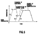
- Fig. 5 is a view to explain the relationship between a time necessary for a process of the growth of a nitride semiconductor on a sapphire substrate and a temperature of a growth furnace.
- reference numeral 51 shows a change with time of the temperature of a growth furnace in the related-art first process in which the temperature is raised to a temperature A (1,000 °C to 1,100 °C), thereby cleaning the sapphire substrate, and the temperature is dropped to a temperature B (400 °C to 600 °C), thereby depositing the buffer layer on the sapphire substrate.
- Reference numeral 52 shows a change with time of the temperature of a growth furnace in the related-art second process in which the temperature is raised to a temperature B (400 °C to 600 °C), thereby depositing the buffer layer on the sapphire substrate.
- Reference numeral 53 shows a change with time of the temperature of a growth furnace according to an example useful for understanding the invention in the third process in which the temperature is raised to a temperature C (1,000 °C), thereby growing the nitride semiconductor on the substrate for growth of nitride semiconductor.
- the first process or second process is performed, thereby forming the buffer layer on the sapphire substrate, and the third process is performed, thereby growing the nitride semiconductor on the buffer layer.
- the third process is performed, thereby growing the nitride semiconductor on the buffer layer.
- the growth sequence is a method in which the substrate 6 for growth of nitride semiconductor was introduced into a growth furnace, the temperature was then raised to the growth temperature (1,000 °C) under an ammonia atmosphere, and a source material gas was supplied. Trimethylgallium, trimethylaluminum and ammonia are used as the source materials.
- a Si was used for dopant of n-type impurities.
- Mg was used for dopant of p-type impurities.
- a mesa structure was prepared by etching, and ohmic electrodes, i.e. , the collector electrode 15, the base electrode 16, and the emitter electrode 17, were formed on the each exposed layers by means of electron beam metal deposition. In a collector current-collector voltage characteristic in common emitter configuration of a fabricatied transistor, current gain of approximately 100 was obtained, and the breakdown voltage was increased to approximately 200 V with a reduction of the dislocation density as described already being reflected.
Description
- The present invention relates to a substrate for growth of nitride semiconductor to be used for growth of a nitride semiconductor on a sapphire substrate.
- Prior art which is related to this field of technology can be found e.g. in document NAKAO W ET AL: "AlN Films Epitaxially formed by direct Nitridation of :Sapphire using Aluminum Oxynitride as a buffer Layer", STATE-OF-THE-ART PROGRAM ON COMPOUND SEMICONDUCTORS XXXVI AND WIDE BANDGAP SEMICONDUCTORS FOR PHOTONIC AND ELECTRONIC DEVICES AND SENSORS II, 1 January 2002 (2002-01-01), pages 76-82, document, document WIDMANN F ET AL: "Low temperature sapphire nitridation: A clue to optimize GaN layers grown by molecular beam epitaxy", JOURNAL OF APPLIED PHYSICS, AMERICAN INSTITUTE OF PHYSICS. NEW YORK, US, vol. 85, no. 3, 1 February 1999 (1999-02-01), pages 1550-1555, document
WO 02/12598 A1 US 5,656,832 disclosing a semiconductor heterojunction device with AlN buffer layer of 3 nm to 10 nm average film thickness. - Since nitride semiconductors have a band gap in the far infrared to ultraviolet wavelength region, they are promising as a material of light emitting or light receiving devices in that region. Also, the nitride semiconductors have a wide band gap and have a large breakdown field and a high saturation electron velocity. For that reason, the nitride semiconductors are also very promising as materials of electronic devices with high-temperature, high output power and high frequency operation. Further, since the nitride semiconductors do not contain arsenic (As) and phosphorus (P), as compared with GaAs based or InP based semiconductors which have hitherto been utilized, they have a merit that they are harmless against the environment and are expected as a semiconductor device material in the future.
- As a substrate for epitaxial growth of nitride semiconductor having such excellent characteristics, any material having a lattice constant and a coefficient of thermal expansion equal to those of the nitride semiconductors has not been available yet. For that reason, sapphire, SiC, or Si is mainly used as the substrate.
- For epitaxial growth of GaN, AlN, InN and their alloyed crystals, a sapphire substrate has hitherto been mainly used. However, there are lattice mismatch of 11 to 23 % and a difference in the coefficient of thermal expansion between the sapphire substrate and the nitride semiconductor. Accordingly, if the nitride semiconductor is grown directly on the sapphire substrate, the three-dimensional growth occurs so that the flatness of the surface in an atomic level becomes worse. For that reason, there was a problem that the nitride semiconductor grown on the sapphire substrate has a number of crystal defects.
- In the case of the epitaxial growth of a nitride semiconductor on the sapphire substrate, it has been reported that crystallinity of GaN was improved by a method using a buffer layer. Its technologies will be described below.
- The first is a growth method of GaN using a low-temperature AlN buffer layer (see the following Non-Patent Document 1). This method is as follows. The sapphire substrate was heated up to the temperature around 1000 °C for surface cleaning in metalorganic vapor phase epitaxy system etc., the temperature was then once dropped. Next, a low-temperature AIN buffer layer was deposited at around 500 °C, and the temperature is again raised. Then, GaN was grown at around 1000 °C. The AlN buffer layer deposited by this method is amorphous and the islands were formed during the temperature rising step due to the solid phase growth of amorphous AIN. As a matter of course, the island shape to be formed varies depending upon the atmosphere in the growth system (apparatus)or the temperature rising rate during the temperature rising. At the beginning of growth of the GaN layer at high temperatures, this island becomes a nucleus, whereby the GaN layer undergoes crystal growth. During that crystal growth, flattening of the GaN layer advances due to the coalescence. GaN undergoes two-dimensional crystal growth on the flattened GaN layer.
- The second is a growth method of GaN using a low-temperature GaN buffer layer (see the following Non-Patent Document 2). This method is as follows. The sapphire substrate was heated up to the temperature around 1000 °C, the temperature was then once dropped. Next, a low-temperature GaN buffer layer was deposited at around 500 °C, and the temperature is again raised. Then, GaN was grown at around 1000 °C . Since GaN is decomposed easily at high temperature as compared with AlN, the nucleus formation in the temperature rising step is not always the same as in the case of AlN, but the subsequent growth process is substantially the same.
- Incidentally, in the crystal growth of nitride semiconductors other than GaN, the same methods as in those described previously are applicable, too. For example, in growth Al1-xGaxN (0 ≤ x < 1) or In1-xGaxN (0 ≤ x < 1) crystals, a low-temperature GaN buffer layer is deposited on the sapphire substrate, then GaN, and Al1-xGaxN or In1-xGaxN was grown. In particular, a method of growth of Al1-xGaxN crystals is described in the following Non-Patent
Document 3. - As described previously, in all of these growth methods, the buffer layer was aimed to achieve lattice matching with the GaN layer, but lattice matching with the substrate was not taken into consideration.
- Also, even if the buffer layer is deposited at a low temperature, the low-temperature buffer layer is amorphous and solid phase growth occurs at the time of temperature rising. For that reason, the lattice mismatch between the buffer layer and the substrate still exists, it is difficult to effectively suppress the generation of crystal defects, and threading dislocation of 109 to 1010 cm-2 exists usually. It is well known that this dislocation deteriorates the characteristics of a fabricated device. For example, shortening of the life of laser and an increase of leak current and a lowering of breakdown voltage of the device. Also, diffusion or segregation of impurities may possibly be promoted due to the existence of the dislocation. Accordingly, reducing the dislocation density in the nitride semiconductor layer is very important for improving the device characteristics, realizing devices which have not been attained so far due to influences of the dislocation and enhancing the controllability in fabrication of a device structure in crystal growth.
- Accordingly, the invention is aimed to provide a substrat for growth of nitride semiconductor capable of obtaining a high-quality nitride semiconductor crystal layer.
- Non-Patent Document 1:
- H. Amano, N. Sawaki, I. Akasaki, and Y. Toyoda, "Metal - organic vapor phase epitaxial growth of a high quality GaN film using an AlN buffer layer", Appl. Phys. Lett., 48, 353 (1986)
- Non-Patent Document 2:
- S. Nakamura, "GaN growth using GaN buffer layer", Jpn. J. Appl. Phys., 30, L1705 (1991)
- Non-Patent Document 3:
- C. Pernot, et al., "Low-intensity ultraviolet photodetectors based on AlGaN", Jpn. J. Appl. Phys., 38, L487 (1999)
- One embodiment of the invention is concerned with a method of growing a nitride semiconductor on a substrate according to claim 1.
- According to the embodiments of the invention as described previously, it is possible to provide a method for growth of a nitride semiconductor capable of obtaining a high-quality nitride semiconductor crystal layer.
-
-
Fig 1 is a cross-sectional schematic view of a substrate for growth of nitride semiconductor according to an example useful for understanding the invention; -
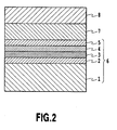
Fig. 2 is a cross-sectional schematic view of a structure in which a GaN layer was epitaxially grown on a substrate for growth of nitride semiconductor according to an example useful for understanding the invention; -
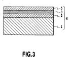
Fig. 3 is a cross-sectional schematic view of a substrate for growth of nitride semiconductor according to an example useful for understanding the invention; -
Fig. 4 is a cross-sectional schematic view of a substrate for growth of nitride semiconductor according to an example useful for understanding the invention; -
Fig. 5 is a view to explain the relationship between a time necessary for a process of forming a nitride semiconductor on a sapphire substrate and a temperature of a growth furnace; -
Fig. 6 is a cross-sectional schematic view of an Al1-xGaxN (0 ≤ x < 1)/GaN heterojunction bipolar transistor structure epitaxially grown on a substrate for growth of nitride semiconductor according to an example useful for understanding the invention. - Examples useful for understanding the invention and embodiments of the invention will be described below in detail with reference to the drawings. Incidentally, in the drawings as described hereinafter, a member having the same functions is given the same symbol, and its explanation is omitted.
-
Fig. 1 is a cross-sectional schematic view of a substrate for growth of nitride semiconductor according to an example useful for understanding the invention. - In
Fig. 1 , reference numeral 1 denotes a sapphire substrate (a sapphire single crystal substrate);reference numeral 2 denotes an Al2O3 layer (an aluminum oxide layer, namely an alumina layer);reference numeral 3 denotes an AlON layer (an aluminum oxynitride layer); reference numeral 4 denotes an AlN layer (an aluminum nitride layer);reference numeral 5 denotes a cap layer (the uppermost layer) made of Al2O3; andreference numeral 6 denotes a substrate for growth of nitride semiconductor. - This example is concerned with a substrate for growth of nitride semiconductor to be used for growth of a nitride semiconductor layer on the sapphire substrate 1 and has a structure having the Al2O3 layer 2 which is separately provided on the sapphire substrate 1, the
AlON layer 3 which is the first layer, and the AlN layer 4 which is the second layer, and theAlON layer 3 and the AlN layer 4 are formed on the foregoing Al2O3 layer 4 in this order. Incidentally, even a structure in which either one layer of theAlON layer 3 as the first layer or the AlN layer 4 as the second layer, each having a composition closed to the nitride semiconductor layer, is provided on the Al2O3 layer 2, gives rise the effects according to the invention and is effective. Also, thecap layer 5 made of Al2O3 is provided as the uppermost layer of thesubstrate 6 for growth of nitride semiconductor. - Incidentally, though the foregoing Al2O3 layer 2 is not always crystalline, it is considered that in the layers, a portion in the crystalline state is lattice-matched with the sapphire substrate 1. The terms "lattice-matched" as referred to herein means that the lattice constant is substantially equal.
- That is, on the sapphire substrate 1 having a diameter of 2 inches, the Al2O3 layer 2 was deposited in a thickness of approximately 5 nm in an Ar plasma at room temperature using Al and oxygen as the sources by an ECR (Electron Cyclotron Resonance) plasma deposition system. Thereafter, nitrogen was added in the deposition chamber, thereby depositing the
AlON layer 3 in a thickness of approximately 10 nm. Next, the AlN layer 4 of the same kind as a nitride semiconductor layer (for example, a GaN layer) to be grown on thesubstrate 6 for growth of nitride semiconductor was deposited in a thickness of approximately 10 nm in an Ar plasma using Al and nitrogen as the sources. Finally, for the purpose of preventing irregular native oxidation which generates surface instability due to stoichiometric disorder, thecap layer 5 made of Al2O3 was deposited in a thickness of approximately 5 nm in an Ar plasma using Al and oxygen as the sources. There was thus prepared thesubstrate 6 for growth of nitride semiconductor. - Incidentally, in the foregoing example, the each layers are formed at room temperature (for example, 20 °C), but the invention is not limited to this temperature. According to one embodiment of the invention, it is important that the substrate for growth of nitride semiconductor according to the invention can be formed even at room temperature, and with respect to the each layers according to one embodiment of the invention, so far as a proper composition of nitrogen and oxygen can be formed, the temperature may be higher or lower than room temperature (the temperature in the atmosphere).
- Also, with respect to the film thickness of the Al2O3 layer 2, the
AlON layer 3 and the AlN layer 4, a thickness at which the film can be formed is necessary, and taking into consideration the lattice constant in the c axis of each compound, a single atomic layer is necessary at the minimum. On the other hand, since each layer of the Al2O3 layer 2, theAlON layer 3 and the AlN layer 4 is not always crystalline (polycrystalline or amorphous), when the film thickness is too thick, it becomes difficult to transfer (epitaxially grow) the crystallographic axis of the sapphire (single crystal) substrate to the nitride semiconductor. In the invention, taking into consideration these matters, it is preferable that the thickness of the Al2O3 layer 2, theAlON layer 3 and the AlN layer 4 is from approximately 1 nm to 200 nm; and it is more preferable that the thickness of the Al2O3 layer 2 is from 2 nm to 20 nm, the thickness of theAlON layer 3 is from 2 nm to 70 nm, and the thickness of the AlN layer 4 is from 2 nm to 50 nm. - Moreover, in the example, the film formation of the each layers is carried out by the ECR plasma deposition system (apparatus), but the invention is not limited thereto. Any apparatus, for example, a MOVPE system having oxygen introduced thereinto, can be employed so far as the film formation of the each layers according to one embodiment of the invention can be properly carried out.
- Next, the experimental results which prove usefulness of the method for growth of nitride semiconductor of the invention will be described below.
-
Fig. 2 is a cross-sectional schematic view of a structure in which a GaN layer was epitaxially grown on the substrate for growth of nitride semiconductor of the invention. - In
Fig. 2 , reference numeral 7 denotes a GaN layer, and reference numeral 8 denotes an Si-doped n-type GaN layer for measuring conductivity. On thesubstrate 6 for growth of nitride semiconductor as illustrated in the foregoing embodiment, the GaN layer 7 was grown by the metalorganic vapor phase epitaxy. In this case, the growth sequence is a simple method in which thesubstrate 6 for growth of nitride semiconductor was introduced into a growth furnace, and thereafter, the temperature was raised to the growth temperature (1,000 °C) under an ammonia atmosphere, thereby growing the GaN layers 7 and 8. Trimethylgallium and ammonia were used as the source materials. For doping n-type impurities of the Si-doped n-type GaN layer 8, a silane was used, thereby forming the Si-doped n-type GaN layer 8. - The grown GaN layers 7 and 8 were subjected to X-ray diffraction measurement and Hall effect measurement, thereby evaluating crystallinity and electric characteristics. The evaluation of crystallinity of the grown GaN layer 7 was carried out by estimating a dislocation density in the crystal from a full width at half maximum of X-ray asymmetric reflection spectrum from (10-10). As a result of estimating the dislocation density, the dislocation density of the related art was approximately 2 × 109 cm-2. On the other hand, in the case of the GaN layer 7 prepared using the
substrate 6 for growth of nitride semiconductor of the foregoing embodiment, the dislocation density was 9 × 107 cm-2 and largely reduced. Also, as a result of the Hall effect measurement, the carrier density and mobility of the related art were 3 × 1017 cm-3 and 340 cm2/Vs, respectively. On the other hand, the carrier density and mobility of the GaN layer 7 prepared using thesubstrate 6 for growth of nitride semiconductor of the foregoing embodiment were 2 × 1017 cm-3 and 540 cm2/Vs, respectively, and it became clear that the characteristics were largely improved. - In the light of the above, according to the method of the invention for growth of nitride semiconductor having the each layers, since the composition of nitrogen and oxygen (ratio of the constitutional atoms) is changed from the each layers which are not always crystalline but are a layer for the purpose of achieving lattice matching with the sapphire single crystal toward the nitride semiconductor to be grown, the lattice spacing or distance between constitutional atoms in each layer changes, and the threading dislocation into the nitride semiconductor crystal is largely reduced as compared with the related art. Accordingly, it is possible to easily prepare a crystal having a dislocation density in the order of 107 cm-2. Namely, in the invention, since the dislocation density can be uniformly reduced over the whole of the substrate surface, it is possible to design to improve the crystallinity of the nitride semiconductor layer, and such is very industrially effective. Also, since an improvement of the crystallinity is anticipated with a reduction of the dislocation density, various ripple effects including an improvement of the device characteristics and realization of new devices are expected.
- Incidentally, the substrate for growth of nitride semiconductor of the invention can also be applied to the growth of crystal of nitride semiconductors other than GaN, Al1-xGaxN (0 ≤ x < 1), In1-xGaxN (0 ≤ x < 1), AlN, InN, etc. Also, the applicable nitride semiconductor layer does not rely upon the presence or absence of doping of impurities, the polarity of a carrier of the semiconductor doped with impurities, and the composition ratio of a alloyed crystal.
- As the general lattice constants of various constitutional elements, etc. of the
substrate 6 for growth of nitride semiconductor in the foregoing embodiment, the following values are known.
Sapphire and Al2O3: a = 4.758 angstrom, c = 12.991 angstrom
AlN: a = 3.112 angstrom, c = 4.982 angstrom
GaN: a = 3.189 angstrom, c = 5.185 angstrom - That is, with respect to the each layers in the method for growth of nitride semiconductor in the embodiment, since the composition of oxygen and nitrogen (ratio of the constitutional atoms) is changed from the sapphire substrate 1 into, for example, an oxide, an oxynitride, and a nitride, the lattice spacing or distance between constitutional atoms in each layer changes.
- In the light of the above, the invention is concerned with the method for growth of nitride semiconductor capable of easy growth of a nitride semiconductor having high-quality crystallinity to crystal growth. For achieving this matter, the invention is characterized in that in the buffer layer to be formed on the sapphire substrate 1, the composition of the buffer layer is changed from the surface contacting with the sapphire substrate 1 toward the surface contacting with the nitride semiconductor layer. By changing the composition (ratio of the constitutional atoms) of the buffer layer, the lattice spacing or distance between constitutional atoms of the buffer layer changes.
- Specifically, the invention is concerned with a layered structure of the sapphire substrate 1, the Al2O3 layer 2, the
AlON layer 3, and the AlN layer 4. According to one embodiment of the invention, in the foregoing buffer layer, the layer contacting with the sapphire substrate 1 is the Al2O3 layer 2 which is not always crystalline but usually lattice-matched with the sapphire substrate in the crystalline state, whereby lattice mismatch between the sapphire substrate and the buffer layer can be reduced although the Al2O3 layer 2 is not always crystalline. Also, in the foregoing buffer layer, by deposition of theAlON layer 3 and the AlN layer 4 which are not always crystalline on the Al2O3 layer 2 to form a nitride semiconductor layer on the AlN layer 4, lattice mismatch between the buffer layer and the nitride semiconductor layer can be reduced although the AlN layer 4 is not always crystalline. Incidentally, with respect to theAlON layer 3 and the AlN layer 4, though it is the best mode that these layers are deposited in that order, similar effects can be obtained even by a structure using either one of theAlON layer 3 or the AlN layer 4 as illustrated inFigs. 3 and4 . - In the light of the above, with respect to the buffer layer to be formed between the sapphire substrate and the nitride semiconductor, what is important in one embodiment of the invention is not only to reduce lattice mismatch of the surface contacting with the nitride semiconductor but also to separately provide a buffer layer constructed so as to reduce lattice mismatch of the surface contacting with the sapphire substrate. For achieving this matter, according to one embodiment of the invention, it is essential that in the buffer layer, the composition of nitrogen and oxygen is changed from the surface of the buffer layer contacting with the sapphire substrate toward the surface contacting with the nitride semiconductor. Namely, it is essential to separately provide a buffer layer on the sapphire substrate such that with respect to the composition of oxygen and nitrogen to be contained in the buffer layer, the buffer layer has an oxygen-rich composition in the vicinity of the surface of the buffer layer contacting with the sapphire substrate, that the buffer layer has a nitrogen-rich composition in the vicinity of the surface of the buffer layer contacting with the nitride semiconductor, and that the composition of nitrogen increases from the vicinity of the sapphire substrate toward the vicinity of the nitride semiconductor substrate.
- According to one embodiment of the invention, the buffer layer may be monocrystalline or polycrystalline or may be an intermediate layer. In this description, the term "intermediate layer" as referred to herein means a layer in which single crystals , polycrystals, and amorphous crystals are mixed.
- For that reason, according to one embodiment of the invention, as illustrated in
Fig. 1 , the buffer layer is constructed such that the Al2O3 layer 2, theAlON layer 3, and the AlN layer 4 are successively deposited and that nitrogen is increased with a gradient from the sapphire substrate 1 toward the GaN layer 7 (not illustrated inFig. 1 ) . Also, as illustrated inFigs. 3 and4 , the buffer layer may be constructed such that the Al2O3 layer and either one of theAlON layer 3 or the AlN layer 4 are deposited and that the composition of nitrogen is stepwise increased from the sapphire substrate 1 toward the GaN layer 7 (not illustrated inFigs. 3 and4 ). - The Al2O3 cap layer according to one embodiment of the invention will be described below in detail.
- The
cap layer 5 made of Al2O3 is provided as the uppermost layer of thesubstrate 6 for growth of nitride semiconductor, and thiscap layer 5 is provided for the purpose of keeping stability against the external environment, such as one to be exposed to air. This structure is different from the structure using the buffer layer according to the related art with respect to the point of the presence or absence of thecap layer 5. Thecap layer 5 enables one to take out thesubstrate 6 for growth of nitride semiconductor into the air atmosphere outside the chamber and makes it easy to handle thesubstrate 6. Incidentally, it is considered that since in this Al2O3 cap layer 5 as the final layer, an atmosphere of a nitrogen-containing substance such as ammonia is used at the time of crystal growth of the nitride semiconductor, thecap layer 5 is changed into AlN which constitutes the AlN layers as its lower layer (however, illustrated as the Al2O3 cap layer 5 inFigs. 2 ,3 and4 andFig. 6 as described later). Namely, thecap layer 5 plays a dual role of a cap which brings about stability and a surface at the time of growth of nitride semiconductor. - Now, since the related-art growth method of nitride semiconductor includes two stages of the growth of the buffer layer as described previously and the temperature-rising and temperature-dropping process, there are encountered such problems that the growth process is complicated and that a time necessary for a process of forming a nitride semiconductor on a sapphire substrate (also referred to as "growth time" in this description) is long.
-
Fig. 5 is a view to explain the relationship between a time necessary for a process of the growth of a nitride semiconductor on a sapphire substrate and a temperature of a growth furnace. InFig. 5 ,reference numeral 51 shows a change with time of the temperature of a growth furnace in the related-art first process in which the temperature is raised to a temperature A (1,000 °C to 1,100 °C), thereby cleaning the sapphire substrate, and the temperature is dropped to a temperature B (400 °C to 600 °C), thereby depositing the buffer layer on the sapphire substrate.Reference numeral 52 shows a change with time of the temperature of a growth furnace in the related-art second process in which the temperature is raised to a temperature B (400 °C to 600 °C), thereby depositing the buffer layer on the sapphire substrate.Reference numeral 53 shows a change with time of the temperature of a growth furnace according to an example useful for understanding the invention in the third process in which the temperature is raised to a temperature C (1,000 °C), thereby growing the nitride semiconductor on the substrate for growth of nitride semiconductor. - According to the related art, in growth of the nitride semiconductor on the sapphire substrate, the first process or second process is performed, thereby forming the buffer layer on the sapphire substrate, and the third process is performed, thereby growing the nitride semiconductor on the buffer layer. At this time, as illustrated by the
reference numeral 51 or thereference numeral 52, since the inside of the growth furnace is set up at high temperatures before growth of the nitride semiconductor, deterioration of the growth apparatus is promoted. It is considered that the degree of deterioration of the growth apparatus is influenced in an exponential function manner by the use temperature and use time. - On the other hand, according to one example useful for understanding the invention, since the substrate for growth of nitride semiconductor can be prepared at room temperature, the growth furnace does not experience the temperature change as illustrated by the
reference numeral 51 orreference numeral 52. Thus, as illustrated by thereference numeral 53, the temperature-rising and temperature-dropping process for forming the buffer layer, which has hitherto been required, is not required, and by raising the temperature to the growth temperature of the nitride semiconductor (1,000 °C), it is possible to easily grow the nitride semiconductor layer. Also, since the time for keeping the temperature within the growth furnace high can be shortened as compared with the related art, it is possible to realize a long life of the mechanism for heating the substrate within the growth furnace and so on. - In an embodiment of the invention using the substrate for growth of nitride semiconductor having an Al2O3 cap layer as the uppermost layer, since the substrate can be exposed in the air, it becomes possible to separately form the substrate and the growth of the nitride semiconductor onto the substrate. Accordingly, in growth of the nitride semiconductor, by using the substrate for growth of nitride semiconductor having an Al2O3 cap layer as separately prepared, it is possible to omit the time for forming the buffer layer on the sapphire substrate. That is, since the procedures can be started from the third process, the growth time can be shortened, leading to an improvement of the productivity. Accordingly, it becomes possible to simplify the growth sequence and to largely shorten the growth time, these aspects having hitherto been problems.
- Next, an application example of the method for growth of nitride semiconductor and a used substrate will be described below.
-
Fig. 6 is a cross-sectional schematic view of an Al1-xGaxN (0 ≤ x < 1)/GaN heterojunction bipolar transistor structure having been subjected to crystal growth on the substrate for growth of nitride semiconductor of the invention. - In
Fig. 6 , reference numeral 9 denotes a GaN buffer layer;reference numeral 10 denotes an n+-type GaN subcollector layer; reference numeral 11 denotes an n--type GaN collector layer;reference numeral 12 denotes a p-type GaN base layer;reference numeral 13 denotes an n--type Al1-xGaxN emitter layer (0 ≤ x < 1);reference numeral 14 denotes an n+-type GaN contact layer;reference numeral 15 denotes a collector electrode;reference numeral 16 denotes a base electrode; and reference numeral 17 denotes an emitter electrode. - On the
substrate 6 for growth of nitride semiconductor as illustrated in the foregoing embodiment, the GaN buffer layer 9 (thickness: 1 µm), the n+-type GaN subcollector layer 10 (thickness: 1 µm), the n--type GaN collector layer 11 (thickness: 0.5 µm), the p-type GaN base layer 12 (thickness: 0.08 µm), the n--type Al1-xGaxN emitter layer 13 (0 ≤ x < 1) (thickness: 0.05 µm), and the n+-type GaN contact layer 14 (thickness: 0.1 µm) were grown by the metalorganic vapor phase epitaxy. In this case, the growth sequence is a method in which thesubstrate 6 for growth of nitride semiconductor was introduced into a growth furnace, the temperature was then raised to the growth temperature (1,000 °C) under an ammonia atmosphere, and a source material gas was supplied. Trimethylgallium, trimethylaluminum and ammonia are used as the source materials. For dopant of n-type impurities, a Si was used. For dopant of p-type impurities, Mg was used. A mesa structure was prepared by etching, and ohmic electrodes, i.e. , thecollector electrode 15, thebase electrode 16, and the emitter electrode 17, were formed on the each exposed layers by means of electron beam metal deposition. In a collector current-collector voltage characteristic in common emitter configuration of a fabricatied transistor, current gain of approximately 100 was obtained, and the breakdown voltage was increased to approximately 200 V with a reduction of the dislocation density as described already being reflected.
Claims (3)
- A method of growing a nitride semiconductor layer (7, 9) on a substrate (6), comprising:providing the substrate (6); andgrowing the nitride semiconductor layer (7, 9) directly onto the cap layer (5) of the substrate (6); wherein the substrate comprises
a single-crystalline sapphire substrate (1);
a layer (2, 3, 4) including N, O and Al which is arranged on the sapphire substrate, wherein the layer is monocrystalline, polycrystalline, or amorphous,
wherein the layer (2, 3, 4) contacts with the sapphire substrate (1) at a first surface thereof and is formed such that a proportion of N in a composition ratio of N, O and Al at the first surface is smaller than that of N in the composition ratio of N, O and Al at a second surface and that a proportion of O in the composition ratio at the first surface is larger than that of O in the composition ratio at the second surface; and
a cap layer (5) made of Al2O3 which is provided on said layer (2, 3, 4), wherein the cap layer is formed on the second surface as an uppermost layer of the substrate. - The method according to claim 1, wherein said layer (2, 3, 4) comprises:an Al2O3 layer (2) on the sapphire substrate (1); andeither one layer of an AlON layer (3) or an AIN layer (4) provided on said Al2O3 layer.
- The method according to claim 1, wherein said layer (2, 3, 4) comprises:an Al2O3 layer (2) on the sapphire substrate (1); anda structure in which a first layer of AlON (3) and a second layer of AlN (4) are arranged on the Al2O3 layer (2) in this order.
Applications Claiming Priority (2)
| Application Number | Priority Date | Filing Date | Title |
|---|---|---|---|
| JP2003292350 | 2003-08-12 | ||
| PCT/JP2004/011539 WO2005015618A1 (en) | 2003-08-12 | 2004-08-11 | Substrate for nitride semiconductor growth |
Publications (3)
| Publication Number | Publication Date |
|---|---|
| EP1655766A1 EP1655766A1 (en) | 2006-05-10 |
| EP1655766A4 EP1655766A4 (en) | 2009-10-21 |
| EP1655766B1 true EP1655766B1 (en) | 2014-04-30 |
Family
ID=34131715
Family Applications (1)
| Application Number | Title | Priority Date | Filing Date |
|---|---|---|---|
| EP04771524.8A Active EP1655766B1 (en) | 2003-08-12 | 2004-08-11 | Substrate for growth of nitride semiconductor |
Country Status (7)
| Country | Link |
|---|---|
| US (1) | US7244520B2 (en) |
| EP (1) | EP1655766B1 (en) |
| JP (1) | JP4249184B2 (en) |
| KR (1) | KR100690413B1 (en) |
| CN (1) | CN100389481C (en) |
| TW (1) | TW200518197A (en) |
| WO (1) | WO2005015618A1 (en) |
Families Citing this family (48)
| Publication number | Priority date | Publication date | Assignee | Title |
|---|---|---|---|---|
| US8545629B2 (en) | 2001-12-24 | 2013-10-01 | Crystal Is, Inc. | Method and apparatus for producing large, single-crystals of aluminum nitride |
| US7638346B2 (en) * | 2001-12-24 | 2009-12-29 | Crystal Is, Inc. | Nitride semiconductor heterostructures and related methods |
| US7641735B2 (en) | 2005-12-02 | 2010-01-05 | Crystal Is, Inc. | Doped aluminum nitride crystals and methods of making them |
| JP2007165478A (en) * | 2005-12-12 | 2007-06-28 | National Univ Corp Shizuoka Univ | Photoelectric surface and photo-detector |
| JP5004597B2 (en) * | 2006-03-06 | 2012-08-22 | シャープ株式会社 | Nitride semiconductor light emitting device and method for manufacturing nitride semiconductor light emitting device |
| US9034103B2 (en) | 2006-03-30 | 2015-05-19 | Crystal Is, Inc. | Aluminum nitride bulk crystals having high transparency to ultraviolet light and methods of forming them |
| US9771666B2 (en) | 2007-01-17 | 2017-09-26 | Crystal Is, Inc. | Defect reduction in seeded aluminum nitride crystal growth |
| CN107059116B (en) | 2007-01-17 | 2019-12-31 | 晶体公司 | Defect reduction in seeded aluminum nitride crystal growth |
| US8080833B2 (en) * | 2007-01-26 | 2011-12-20 | Crystal Is, Inc. | Thick pseudomorphic nitride epitaxial layers |
| WO2008094464A2 (en) * | 2007-01-26 | 2008-08-07 | Crystal Is, Inc. | Thick pseudomorphic nitride epitaxial layers |
| JP2008214132A (en) * | 2007-03-05 | 2008-09-18 | Univ Of Tokushima | Group iii nitride semiconductor thin film, group iii nitride semiconductor light-emitting element, and method for manufacturing group iii nitride semiconductor thin film |
| JP2009274945A (en) * | 2008-04-17 | 2009-11-26 | Sumitomo Electric Ind Ltd | METHOD OF GROWING AlN CRYSTAL, AND AlN LAMINATE |
| JP5451280B2 (en) * | 2008-10-09 | 2014-03-26 | キヤノン株式会社 | Wurtzite crystal growth substrate, manufacturing method thereof, and semiconductor device |
| JP4933513B2 (en) * | 2008-10-14 | 2012-05-16 | 日本電信電話株式会社 | Nitride semiconductor growth substrate |
| US8704239B2 (en) * | 2009-11-10 | 2014-04-22 | Tokuyama Corporation | Production method of a layered body |
| EP2544250B1 (en) * | 2010-03-01 | 2020-01-08 | Sharp Kabushiki Kaisha | Process for production of nitride semiconductor element, nitride semiconductor light-emitting element, and light-emitting device |
| WO2011155502A1 (en) * | 2010-06-11 | 2011-12-15 | Semiconductor Energy Laboratory Co., Ltd. | Semiconductor device and method for manufacturing the same |
| EP2588651B1 (en) | 2010-06-30 | 2020-01-08 | Crystal Is, Inc. | Growth of large aluminum nitride single crystals with thermal-gradient control |
| US8574728B2 (en) | 2011-03-15 | 2013-11-05 | Kennametal Inc. | Aluminum oxynitride coated article and method of making the same |
| US8778783B2 (en) | 2011-05-20 | 2014-07-15 | Applied Materials, Inc. | Methods for improved growth of group III nitride buffer layers |
| US8853086B2 (en) | 2011-05-20 | 2014-10-07 | Applied Materials, Inc. | Methods for pretreatment of group III-nitride depositions |
| US8980002B2 (en) * | 2011-05-20 | 2015-03-17 | Applied Materials, Inc. | Methods for improved growth of group III nitride semiconductor compounds |
| US8962359B2 (en) | 2011-07-19 | 2015-02-24 | Crystal Is, Inc. | Photon extraction from nitride ultraviolet light-emitting devices |
| US8633094B2 (en) * | 2011-12-01 | 2014-01-21 | Power Integrations, Inc. | GaN high voltage HFET with passivation plus gate dielectric multilayer structure |
| EP2822026B1 (en) * | 2012-02-29 | 2018-03-14 | Kyocera Corporation | Composite substrate |
| DE102012103686B4 (en) * | 2012-04-26 | 2021-07-08 | OSRAM Opto Semiconductors Gesellschaft mit beschränkter Haftung | Epitaxial substrate, method for producing an epitaxial substrate and optoelectronic semiconductor chip with an epitaxial substrate |
| US9718249B2 (en) | 2012-11-16 | 2017-08-01 | Apple Inc. | Laminated aluminum oxide cover component |
| US9138864B2 (en) | 2013-01-25 | 2015-09-22 | Kennametal Inc. | Green colored refractory coatings for cutting tools |
| US9017809B2 (en) | 2013-01-25 | 2015-04-28 | Kennametal Inc. | Coatings for cutting tools |
| US8928037B2 (en) | 2013-02-28 | 2015-01-06 | Power Integrations, Inc. | Heterostructure power transistor with AlSiN passivation layer |
| US9299880B2 (en) | 2013-03-15 | 2016-03-29 | Crystal Is, Inc. | Pseudomorphic electronic and optoelectronic devices having planar contacts |
| EP2778252A3 (en) * | 2013-03-15 | 2014-12-10 | Apple Inc. | Layered Coatings For Sapphire Structure |
| DE102013004558B4 (en) * | 2013-03-18 | 2018-04-05 | Apple Inc. | Method for producing a surface-strained sapphire disk, surface-strained sapphire disk and electrical device with a transparent cover |
| US9427808B2 (en) | 2013-08-30 | 2016-08-30 | Kennametal Inc. | Refractory coatings for cutting tools |
| JP2015168594A (en) * | 2014-03-06 | 2015-09-28 | 日本電信電話株式会社 | Growth method of nitride semiconductor |
| JP6271390B2 (en) * | 2014-10-17 | 2018-01-31 | 日本電信電話株式会社 | Nitride semiconductor crystal growth method |
| JP6872724B2 (en) * | 2015-02-18 | 2021-05-19 | 国立大学法人東北大学 | Nitride semiconductor self-supporting substrate manufacturing method |
| CN105336579B (en) * | 2015-09-29 | 2018-07-10 | 安徽三安光电有限公司 | A kind of semiconductor element and preparation method thereof |
| CN106025026B (en) * | 2016-07-15 | 2018-06-19 | 厦门乾照光电股份有限公司 | It is a kind of for AlN buffer layers of light emitting diode and preparation method thereof |
| DE102016114250B4 (en) * | 2016-08-02 | 2020-04-16 | Forschungsverbund Berlin E.V. | Process for producing a sapphire substrate coated with a semiconductor material, coated sapphire substrate obtainable by the process, and use of such a substrate in a light-emitting diode |
| US20180182916A1 (en) * | 2016-12-26 | 2018-06-28 | Toyoda Gosei Co., Ltd. | Group iii nitride semiconductor light-emitting device and production method therefor |
| US11773508B2 (en) | 2017-09-11 | 2023-10-03 | Tdk Corporation | Substrate and light-emitting element |
| CN108565322A (en) * | 2018-06-01 | 2018-09-21 | 广东工业大学 | A kind of LED epitaxial chips and a kind of preparation method of LED epitaxial chips |
| CN108682724A (en) * | 2018-06-01 | 2018-10-19 | 广东工业大学 | A kind of LED epitaxial chips and a kind of preparation method of LED epitaxial chips |
| CN109065685A (en) * | 2018-08-20 | 2018-12-21 | 浙江大学 | A kind of sapphire compound substrate containing AlN sandwich structure |
| JP7147972B2 (en) * | 2019-05-29 | 2022-10-05 | 日本電信電話株式会社 | Heterojunction bipolar transistor and fabrication method thereof |
| US11269374B2 (en) | 2019-09-11 | 2022-03-08 | Apple Inc. | Electronic device with a cover assembly having an adhesion layer |
| CN113120856B (en) * | 2021-03-24 | 2023-10-13 | 西安电子科技大学 | AlON rectangular nano array based on sapphire substrate and preparation method thereof |
Citations (1)
| Publication number | Priority date | Publication date | Assignee | Title |
|---|---|---|---|---|
| US5656832A (en) * | 1994-03-09 | 1997-08-12 | Kabushiki Kaisha Toshiba | Semiconductor heterojunction device with ALN buffer layer of 3nm-10nm average film thickness |
Family Cites Families (8)
| Publication number | Priority date | Publication date | Assignee | Title |
|---|---|---|---|---|
| JPH02141495A (en) * | 1988-11-21 | 1990-05-30 | Asahi Chem Ind Co Ltd | Laminated single crystal substrate having thin aluminum nitride single crystal film and production thereof |
| JP3020395B2 (en) * | 1993-10-06 | 2000-03-15 | アルプス電気株式会社 | Optical element |
| US5741724A (en) * | 1996-12-27 | 1998-04-21 | Motorola | Method of growing gallium nitride on a spinel substrate |
| JPH1160395A (en) | 1997-08-21 | 1999-03-02 | Fujitsu Ltd | Compound semiconductor device |
| JPH11340147A (en) | 1998-05-25 | 1999-12-10 | Matsushita Electron Corp | Manufacture of nitride semiconductor wafer and element |
| JP2001196697A (en) * | 2000-01-13 | 2001-07-19 | Fuji Photo Film Co Ltd | Substrate for semiconductor element and its manufacturing method, and semiconductor element using the same |
| US6451711B1 (en) | 2000-05-04 | 2002-09-17 | Osemi, Incorporated | Epitaxial wafer apparatus |
| US6744076B2 (en) * | 2002-03-14 | 2004-06-01 | The Circle For The Promotion Of Science And Engineering | Single crystalline aluminum nitride film, method of forming the same, base substrate for group III element nitride film, light emitting device and surface acoustic wave device |
-
2004
- 2004-08-11 CN CNB200480001328XA patent/CN100389481C/en active Active
- 2004-08-11 JP JP2005513005A patent/JP4249184B2/en active Active
- 2004-08-11 WO PCT/JP2004/011539 patent/WO2005015618A1/en active IP Right Grant
- 2004-08-11 KR KR1020057007350A patent/KR100690413B1/en active IP Right Grant
- 2004-08-11 US US10/532,782 patent/US7244520B2/en active Active
- 2004-08-11 EP EP04771524.8A patent/EP1655766B1/en active Active
- 2004-08-12 TW TW093124267A patent/TW200518197A/en unknown
Patent Citations (1)
| Publication number | Priority date | Publication date | Assignee | Title |
|---|---|---|---|---|
| US5656832A (en) * | 1994-03-09 | 1997-08-12 | Kabushiki Kaisha Toshiba | Semiconductor heterojunction device with ALN buffer layer of 3nm-10nm average film thickness |
Non-Patent Citations (1)
| Title |
|---|
| NAKAO W ET AL: "Single crystalline AlN film formed by direct nitridation of sapphire using aluminum oxynitride buffer", JOURNAL OF CRYSTAL GROWTH, ELSEVIER, AMSTERDAM, NL, vol. 259, no. 3, 1 December 2003 (2003-12-01), pages 302 - 308, XP002570964, ISSN: 0022-0248, [retrieved on 20031004], DOI: 10.1016/J.JCRYSGRO.2003.07.026 * |
Also Published As
| Publication number | Publication date |
|---|---|
| EP1655766A1 (en) | 2006-05-10 |
| KR100690413B1 (en) | 2007-03-12 |
| US7244520B2 (en) | 2007-07-17 |
| CN1706030A (en) | 2005-12-07 |
| TWI305660B (en) | 2009-01-21 |
| EP1655766A4 (en) | 2009-10-21 |
| JP4249184B2 (en) | 2009-04-02 |
| US20060051554A1 (en) | 2006-03-09 |
| TW200518197A (en) | 2005-06-01 |
| KR20050062640A (en) | 2005-06-23 |
| JPWO2005015618A1 (en) | 2006-10-05 |
| CN100389481C (en) | 2008-05-21 |
| WO2005015618A1 (en) | 2005-02-17 |
Similar Documents
| Publication | Publication Date | Title |
|---|---|---|
| EP1655766B1 (en) | Substrate for growth of nitride semiconductor | |
| JP5792209B2 (en) | Method for heteroepitaxial growth of high quality N-plane GaN, InN and AlN and their alloys by metalorganic chemical vapor deposition | |
| TWI501291B (en) | Method for forming epitaxial wafers and method for fabricating semiconductor elements | |
| JP3866540B2 (en) | Nitride semiconductor device and manufacturing method thereof | |
| US7951685B2 (en) | Method for manufacturing semiconductor epitaxial crystal substrate | |
| WO2012164750A1 (en) | Nitride electronic device and method for manufacturing nitride electronic device | |
| EP2832900B1 (en) | Laminated substate of silicon single crystal and group iii nitride single crystal with off angle | |
| JP4468744B2 (en) | Method for producing nitride semiconductor thin film | |
| JP2010073750A (en) | Method for growing zinc-oxide-based semiconductor, and method for manufacturing semiconductor light emitting element | |
| JP4429459B2 (en) | Method for producing high-resistance GaN crystal layer | |
| JPH08186332A (en) | Manufacture of semiconductor element | |
| JP5746927B2 (en) | Semiconductor substrate, semiconductor device, and method of manufacturing semiconductor substrate | |
| JP2003178976A (en) | Semiconductor device, and method for manufacturing it | |
| WO2012137309A1 (en) | Method for manufacturing nitride electronic devices | |
| KR100935974B1 (en) | Manufacturing method of Nitride semiconductor light emitting devide | |
| JP2004235193A (en) | Manufacturing method for nitride iii-v compound semiconductor device and nitride iii-v compound semiconductor device | |
| JP4051311B2 (en) | Nitride semiconductor crystal growth method | |
| JP3152152B2 (en) | Compound semiconductor epitaxial wafer | |
| JP2004099405A (en) | Nitride semiconductor multilayer material and method of growing the same | |
| JPH0529653A (en) | Semiconductor device | |
| KR100295022B1 (en) | Method for fabricating a nitride compound semiconductor | |
| JP2005045153A (en) | Manufacturing method of nitride semiconductor, semiconductor wafer, and semiconductor device | |
| JP2004056114A (en) | Semiconductor device | |
| JPH10214999A (en) | Iii-v nitride semiconductor device | |
| JP5614057B2 (en) | Method for fabricating a nitride electronic device |
Legal Events
| Date | Code | Title | Description |
|---|---|---|---|
| PUAI | Public reference made under article 153(3) epc to a published international application that has entered the european phase |
Free format text: ORIGINAL CODE: 0009012 |
|
| 17P | Request for examination filed |
Effective date: 20050428 |
|
| AK | Designated contracting states |
Kind code of ref document: A1 Designated state(s): DE FR GB |
|
| DAX | Request for extension of the european patent (deleted) | ||
| RBV | Designated contracting states (corrected) |
Designated state(s): DE FR GB |
|
| A4 | Supplementary search report drawn up and despatched |
Effective date: 20090916 |
|
| RIC1 | Information provided on ipc code assigned before grant |
Ipc: C30B 25/18 20060101ALI20090910BHEP Ipc: H01L 21/20 20060101AFI20050224BHEP |
|
| 17Q | First examination report despatched |
Effective date: 20091218 |
|
| RIC1 | Information provided on ipc code assigned before grant |
Ipc: H01L 21/20 20060101AFI20130424BHEP Ipc: C30B 25/18 20060101ALI20130424BHEP Ipc: C30B 29/40 20060101ALI20130424BHEP |
|
| GRAP | Despatch of communication of intention to grant a patent |
Free format text: ORIGINAL CODE: EPIDOSNIGR1 |
|
| INTG | Intention to grant announced |
Effective date: 20130621 |
|
| GRAP | Despatch of communication of intention to grant a patent |
Free format text: ORIGINAL CODE: EPIDOSNIGR1 |
|
| INTG | Intention to grant announced |
Effective date: 20131115 |
|
| GRAS | Grant fee paid |
Free format text: ORIGINAL CODE: EPIDOSNIGR3 |
|
| GRAA | (expected) grant |
Free format text: ORIGINAL CODE: 0009210 |
|
| AK | Designated contracting states |
Kind code of ref document: B1 Designated state(s): DE FR GB |
|
| REG | Reference to a national code |
Ref country code: GB Ref legal event code: FG4D |
|
| REG | Reference to a national code |
Ref country code: DE Ref legal event code: R096 Ref document number: 602004044965 Country of ref document: DE Effective date: 20140612 |
|
| REG | Reference to a national code |
Ref country code: DE Ref legal event code: R097 Ref document number: 602004044965 Country of ref document: DE |
|
| PLBE | No opposition filed within time limit |
Free format text: ORIGINAL CODE: 0009261 |
|
| STAA | Information on the status of an ep patent application or granted ep patent |
Free format text: STATUS: NO OPPOSITION FILED WITHIN TIME LIMIT |
|
| 26N | No opposition filed |
Effective date: 20150202 |
|
| REG | Reference to a national code |
Ref country code: DE Ref legal event code: R097 Ref document number: 602004044965 Country of ref document: DE Effective date: 20150202 |
|
| REG | Reference to a national code |
Ref country code: FR Ref legal event code: PLFP Year of fee payment: 13 |
|
| REG | Reference to a national code |
Ref country code: FR Ref legal event code: PLFP Year of fee payment: 14 |
|
| REG | Reference to a national code |
Ref country code: FR Ref legal event code: PLFP Year of fee payment: 15 |
|
| PGFP | Annual fee paid to national office [announced via postgrant information from national office to epo] |
Ref country code: GB Payment date: 20230824 Year of fee payment: 20 |
|
| PGFP | Annual fee paid to national office [announced via postgrant information from national office to epo] |
Ref country code: FR Payment date: 20230822 Year of fee payment: 20 Ref country code: DE Payment date: 20230821 Year of fee payment: 20 |