EP1672972A1 - Electronic circuit device and production method of the same - Google Patents
Electronic circuit device and production method of the same Download PDFInfo
- Publication number
- EP1672972A1 EP1672972A1 EP05017765A EP05017765A EP1672972A1 EP 1672972 A1 EP1672972 A1 EP 1672972A1 EP 05017765 A EP05017765 A EP 05017765A EP 05017765 A EP05017765 A EP 05017765A EP 1672972 A1 EP1672972 A1 EP 1672972A1
- Authority
- EP
- European Patent Office
- Prior art keywords
- resin
- circuit device
- electronic circuit
- connector
- concave
- Prior art date
- Legal status (The legal status is an assumption and is not a legal conclusion. Google has not performed a legal analysis and makes no representation as to the accuracy of the status listed.)
- Granted
Links
- 238000004519 manufacturing process Methods 0.000 title claims description 12
- 229910052751 metal Inorganic materials 0.000 claims abstract description 111
- 239000002184 metal Substances 0.000 claims abstract description 111
- 229920005989 resin Polymers 0.000 claims abstract description 30
- 239000011347 resin Substances 0.000 claims abstract description 30
- 238000007789 sealing Methods 0.000 claims abstract description 24
- 238000002347 injection Methods 0.000 claims description 3
- 239000007924 injection Substances 0.000 claims description 3
- 238000010276 construction Methods 0.000 description 19
- 238000000034 method Methods 0.000 description 16
- 239000000463 material Substances 0.000 description 14
- 230000001681 protective effect Effects 0.000 description 11
- 239000003822 epoxy resin Substances 0.000 description 7
- 229920000647 polyepoxide Polymers 0.000 description 7
- 230000035882 stress Effects 0.000 description 7
- 238000000465 moulding Methods 0.000 description 6
- 238000004891 communication Methods 0.000 description 5
- 238000001721 transfer moulding Methods 0.000 description 5
- 238000003825 pressing Methods 0.000 description 4
- 239000000126 substance Substances 0.000 description 4
- 230000008901 benefit Effects 0.000 description 3
- 230000009467 reduction Effects 0.000 description 3
- 239000004065 semiconductor Substances 0.000 description 3
- 238000005476 soldering Methods 0.000 description 3
- 238000005538 encapsulation Methods 0.000 description 2
- LNEPOXFFQSENCJ-UHFFFAOYSA-N haloperidol Chemical compound C1CC(O)(C=2C=CC(Cl)=CC=2)CCN1CCCC(=O)C1=CC=C(F)C=C1 LNEPOXFFQSENCJ-UHFFFAOYSA-N 0.000 description 2
- 238000005259 measurement Methods 0.000 description 2
- 229920001187 thermosetting polymer Polymers 0.000 description 2
- 238000012546 transfer Methods 0.000 description 2
- XLYOFNOQVPJJNP-UHFFFAOYSA-N water Substances O XLYOFNOQVPJJNP-UHFFFAOYSA-N 0.000 description 2
- HBBGRARXTFLTSG-UHFFFAOYSA-N Lithium ion Chemical compound [Li+] HBBGRARXTFLTSG-UHFFFAOYSA-N 0.000 description 1
- 238000010521 absorption reaction Methods 0.000 description 1
- 238000005452 bending Methods 0.000 description 1
- 235000013361 beverage Nutrition 0.000 description 1
- 230000001413 cellular effect Effects 0.000 description 1
- 239000000919 ceramic Substances 0.000 description 1
- 230000008859 change Effects 0.000 description 1
- 239000000428 dust Substances 0.000 description 1
- 230000000694 effects Effects 0.000 description 1
- 239000013013 elastic material Substances 0.000 description 1
- 230000002708 enhancing effect Effects 0.000 description 1
- 239000000446 fuel Substances 0.000 description 1
- 238000010438 heat treatment Methods 0.000 description 1
- 238000009434 installation Methods 0.000 description 1
- 229910001416 lithium ion Inorganic materials 0.000 description 1
- 238000003754 machining Methods 0.000 description 1
- 238000012423 maintenance Methods 0.000 description 1
- 239000003921 oil Substances 0.000 description 1
- 230000000704 physical effect Effects 0.000 description 1
- 230000005855 radiation Effects 0.000 description 1
- 239000000725 suspension Substances 0.000 description 1
- 230000008646 thermal stress Effects 0.000 description 1
- 239000002699 waste material Substances 0.000 description 1
- 238000004078 waterproofing Methods 0.000 description 1
Images


Classifications
-
- H—ELECTRICITY
- H05—ELECTRIC TECHNIQUES NOT OTHERWISE PROVIDED FOR
- H05K—PRINTED CIRCUITS; CASINGS OR CONSTRUCTIONAL DETAILS OF ELECTRIC APPARATUS; MANUFACTURE OF ASSEMBLAGES OF ELECTRICAL COMPONENTS
- H05K5/00—Casings, cabinets or drawers for electric apparatus
- H05K5/06—Hermetically-sealed casings
- H05K5/065—Hermetically-sealed casings sealed by encapsulation, e.g. waterproof resin forming an integral casing, injection moulding
-
- H—ELECTRICITY
- H05—ELECTRIC TECHNIQUES NOT OTHERWISE PROVIDED FOR
- H05K—PRINTED CIRCUITS; CASINGS OR CONSTRUCTIONAL DETAILS OF ELECTRIC APPARATUS; MANUFACTURE OF ASSEMBLAGES OF ELECTRICAL COMPONENTS
- H05K3/00—Apparatus or processes for manufacturing printed circuits
- H05K3/22—Secondary treatment of printed circuits
- H05K3/28—Applying non-metallic protective coatings
- H05K3/284—Applying non-metallic protective coatings for encapsulating mounted components
-
- H—ELECTRICITY
- H05—ELECTRIC TECHNIQUES NOT OTHERWISE PROVIDED FOR
- H05K—PRINTED CIRCUITS; CASINGS OR CONSTRUCTIONAL DETAILS OF ELECTRIC APPARATUS; MANUFACTURE OF ASSEMBLAGES OF ELECTRICAL COMPONENTS
- H05K5/00—Casings, cabinets or drawers for electric apparatus
- H05K5/0026—Casings, cabinets or drawers for electric apparatus provided with connectors and printed circuit boards [PCB], e.g. automotive electronic control units
- H05K5/0034—Casings, cabinets or drawers for electric apparatus provided with connectors and printed circuit boards [PCB], e.g. automotive electronic control units having an overmolded housing covering the PCB
-
- H—ELECTRICITY
- H01—ELECTRIC ELEMENTS
- H01L—SEMICONDUCTOR DEVICES NOT COVERED BY CLASS H10
- H01L2924/00—Indexing scheme for arrangements or methods for connecting or disconnecting semiconductor or solid-state bodies as covered by H01L24/00
- H01L2924/0001—Technical content checked by a classifier
- H01L2924/0002—Not covered by any one of groups H01L24/00, H01L24/00 and H01L2224/00
-
- H—ELECTRICITY
- H05—ELECTRIC TECHNIQUES NOT OTHERWISE PROVIDED FOR
- H05K—PRINTED CIRCUITS; CASINGS OR CONSTRUCTIONAL DETAILS OF ELECTRIC APPARATUS; MANUFACTURE OF ASSEMBLAGES OF ELECTRICAL COMPONENTS
- H05K1/00—Printed circuits
- H05K1/02—Details
- H05K1/11—Printed elements for providing electric connections to or between printed circuits
- H05K1/117—Pads along the edge of rigid circuit boards, e.g. for pluggable connectors
-
- H—ELECTRICITY
- H05—ELECTRIC TECHNIQUES NOT OTHERWISE PROVIDED FOR
- H05K—PRINTED CIRCUITS; CASINGS OR CONSTRUCTIONAL DETAILS OF ELECTRIC APPARATUS; MANUFACTURE OF ASSEMBLAGES OF ELECTRICAL COMPONENTS
- H05K2201/00—Indexing scheme relating to printed circuits covered by H05K1/00
- H05K2201/10—Details of components or other objects attached to or integrated in a printed circuit board
- H05K2201/10007—Types of components
- H05K2201/10189—Non-printed connector
-
- H—ELECTRICITY
- H05—ELECTRIC TECHNIQUES NOT OTHERWISE PROVIDED FOR
- H05K—PRINTED CIRCUITS; CASINGS OR CONSTRUCTIONAL DETAILS OF ELECTRIC APPARATUS; MANUFACTURE OF ASSEMBLAGES OF ELECTRICAL COMPONENTS
- H05K2203/00—Indexing scheme relating to apparatus or processes for manufacturing printed circuits covered by H05K3/00
- H05K2203/11—Treatments characterised by their effect, e.g. heating, cooling, roughening
- H05K2203/1147—Sealing or impregnating, e.g. of pores
-
- Y—GENERAL TAGGING OF NEW TECHNOLOGICAL DEVELOPMENTS; GENERAL TAGGING OF CROSS-SECTIONAL TECHNOLOGIES SPANNING OVER SEVERAL SECTIONS OF THE IPC; TECHNICAL SUBJECTS COVERED BY FORMER USPC CROSS-REFERENCE ART COLLECTIONS [XRACs] AND DIGESTS
- Y10—TECHNICAL SUBJECTS COVERED BY FORMER USPC
- Y10T—TECHNICAL SUBJECTS COVERED BY FORMER US CLASSIFICATION
- Y10T29/00—Metal working
- Y10T29/49—Method of mechanical manufacture
- Y10T29/49002—Electrical device making
- Y10T29/49117—Conductor or circuit manufacturing
- Y10T29/49124—On flat or curved insulated base, e.g., printed circuit, etc.
- Y10T29/4913—Assembling to base an electrical component, e.g., capacitor, etc.
- Y10T29/49146—Assembling to base an electrical component, e.g., capacitor, etc. with encapsulating, e.g., potting, etc.
-
- Y—GENERAL TAGGING OF NEW TECHNOLOGICAL DEVELOPMENTS; GENERAL TAGGING OF CROSS-SECTIONAL TECHNOLOGIES SPANNING OVER SEVERAL SECTIONS OF THE IPC; TECHNICAL SUBJECTS COVERED BY FORMER USPC CROSS-REFERENCE ART COLLECTIONS [XRACs] AND DIGESTS
- Y10—TECHNICAL SUBJECTS COVERED BY FORMER USPC
- Y10T—TECHNICAL SUBJECTS COVERED BY FORMER US CLASSIFICATION
- Y10T29/00—Metal working
- Y10T29/49—Method of mechanical manufacture
- Y10T29/49002—Electrical device making
- Y10T29/49117—Conductor or circuit manufacturing
- Y10T29/49169—Assembling electrical component directly to terminal or elongated conductor
- Y10T29/49171—Assembling electrical component directly to terminal or elongated conductor with encapsulating
- Y10T29/49172—Assembling electrical component directly to terminal or elongated conductor with encapsulating by molding of insulating material
Definitions
- the present invention relates to an electronic circuit device having a printed circuit board. More particularly, it relates to an electronic circuit device favorably used in various modules for use in automobiles, motorcycles, agricultural machines, industrial machines, shipboard machines, and the like.
- modular electronic circuit devices With respect to automobiles, motorcycles, agricultural machines, machining tools, shipboard machines, and the like, modular electronic circuit devices are used. Such modular electronic circuit devices include engine control modules, motor control modules, and automatic shift control modules. These modules are disposed in vehicle compartments or engine rooms. These modules typically adopt such a construction that a printed circuit board mounting electronic components is fixed on a metal base and they are covered with a cover or a casing.
- Japanese Patent Laid-Open No. 2004-111435 discloses an example of an electronic control circuit device using a printed circuit board, which can adopt the on-engine method.
- the electronic control circuit device according to the patent document is formed integrally by transfer molding a connector and a printed wiring board .
- Patent Document 1 Japanese Patent Laid-Open No: 2004-111435
- An object of the present invention is to provide an electronic circuit device that allows downsizing and cost reduction with reliability.
- an electronic circuit device comprises: a circuit board mounting an electronic component; a resin-molded portion formed of resin for covering the electronic component are covered therewith; a convex connector that has a metal terminal for connection and is exposed from the resin-molded portion; and a sealing member wrapped around the resin-molded portion.
- an electronic circuit device that allows downsizing and cost reduction with high reliability.
- the electronic circuit device 10 in this example comprises a circuit board 11, a convex connector 12, a resin-molded portion 15, and a sealing member 16.
- the circuit board 11 is mounted with electronic components, such as a board insert type electronic component 111, a surface mount large electronic component 112, an IC 113, a high heat producing electronic component 114, a surface mount chip-type electronic component 115 , a back mount chip-type electronic component 116, and the like.
- These electronic components 111 to 116 are covered with the single resin-molded portion 15.
- the electronic circuit device 10 in this example is of resin mold type.
- thermosetting resins may be used for the material of the resin-molded portion 15.
- an epoxy resin for transfer mold that is used in common for semiconductor encapsulation may be used. If there is a great difference in coefficient of thermal expansion between the circuit board 11 and the resin-molded portion 15, a problem results: the electronic circuit device 10 is deformed by thermal stress, and may be broken in some cases. Therefore, it is desirable that the thermal expansion coefficient of a resin used for the resin-molded portion 15 should be close to the thermal expansion coefficient of the main material of the circuit board 11 as much as possible.
- a printed circuit board made mostly from epoxy resin may be used for the circuit board 11.
- an epoxy resin for transfer molding a thermal expansion coefficient of the resin being 8 to 18 ⁇ 10 -6 /K, is suitable for the material of the resin-molded portion 15.
- a major application of epoxy resins for transfer molding is semiconductor encapsulation, and it is usually used for products smaller than the electronic circuit device 10 in this example. Therefore, many epoxy resins for transfer molding are short in a spiral flow, which is a distance by which a resin can flow from time when it is heated during resin molding to time when it is hardened under heating. Consequently, when an epoxy resin for transfer mold is used for the material of the resin-molded portion 15, it is required to select one whose spiral flow is equal to or longer than the size of the electronic circuit device 10.
- FIG. 2 is an enlarged cross sectional view of an end of the electronic circuit device 10 illustrated in FIG. 1.
- the convex connector 12 is formed by extending the circuit board 11. That is, the convex connector 12 is formed simultaneously with the circuit board 11 in the production process of the circuit board 11. Therefore, the convex connector 12 is formed of the same material as that of the circuit board 11.
- the upper face and lower face of the convex connector 12 are respectively provided with metal terminals 13 and 14 for connection.
- These metal terminals 13 and 14 for connection are formed by extending metal wirings 117 formed on the front face of the circuit board 11 and metal wirings 118 formed on its back face. That is, the metal terminals 13 and 14 for connection of the convex connector 12 are formed simultaneously with the metal wirings 117 and 118 of the circuit board 11 in the production process of the circuit board 11.
- the sealing member 16 is formed along the periphery of the resin-molded portion 15, in proximity to the convex connector 12. A groove for receiving the sealing member 16 is formed along the periphery of the resin-molded portion 15. When the convex connector 12 is connected with a concave connector, the sealing member 16 provides a waterproof construction for the joint.
- the sealing member 16 may be formed of any material as long as it is an elastic material having heat resistance, oil resistance, resistance to chemicals, and the like. For example, it may be formed of rubber, resin, or the like.
- the sectional shape of the sealing member 16 includes two crests and one trough.
- a construction having at least two crests and at least one trough is desirable. Constructing the sealing member having the sectional shape including two crests brings the following advantage. When the convex connector 12 is connected with a concave connector, the crests of the sealing member are easily deformed. Therefore, the force required for inserting/withdrawing the convex connector 12 is reduced, and the workability in installing the electronic circuit device 10 can be enhanced.
- the sections of the sealing member 16 may be in any other shape as long as a sufficient waterproofing function can be provided.
- the O-ring 17 provided at the base of the convex connector 12 is used to prevent resin from leaking to the convex connector 12 when the circuit board 11 is encapsulated with the resin. This will be described later.
- FIG. 3 is an enlarged view of the convex connector 12 in FIG. 1 as viewed from above A
- FIG. 4 is an enlarged view of the convex connector 12 in FIG. 1 as viewed from left B.
- the metal terminals 13 and 14 for connection of the convex connector 12 are a plurality of strips so formed that they are arranged in parallel with one another at equal intervals.
- any other configuration may be adopted.
- the metal terminals 13 for connection on the upper face and the metal terminals 14 for connection on the lower face are identical in shape with each other. Therefore, both are symmetrical with each other.
- the metal terminals 13 and 14 for connection are formed on both faces of the convex connector 12. Instead, the metal terminals for connection may be provided on one face.
- the metal terminals 13 for connection only on the upper face and the metal terminals 14 for connection on the lower face may be disposed in a staggered configuration as long as they are identical in dimensions with each other.
- the convex connector 12 is provided on one side of the circuit board 11. Instead, the convex connector may be provided on two opposite sides, on three sides, or on all the four sides. If the convex connector 12 is provided on a plurality of sides, the sealing member 16 is provided in correspondence with each of the convex connectors 12.
- FIG. 5 illustrates the convex connector 12 of the electronic circuit device 10 in FIG. 1 as is connected with a concave connector 40.
- the concave connector 40 has a concave portion 42 formed in its housing 41, and a hole 43 is formed in the bottom of the concave portion 42. In this hole 43, metal terminals 44 and 45 for connection and a receiving member 46 are provided.
- the metal terminals 44 and 45 for connection have spring constructions formed by folding strip-shaped metal plates.
- the metal terminals 44 and 45 for connection are connected with harnesses 47. Watertight plugs 48 are installed around the harnesses 47 for connection.
- the convex connector 12 of the electronic circuit device 10 When the convex connector 12 of the electronic circuit device 10 is inserted into the concave portion 42 of the housing 41, the following takes place: the end of the convex connector 12 goes into between two metal terminals 44 and 45 for connection. As a result, the metal terminals 44 and 45 for connection are brought into contact with the metal terminals 13 and 14 for connection of the convex connector 12.
- the convex connector 12 of the electronic circuit device 10 is further inserted into the concave portion 42 of the housing 41, the following takes place: the convex connector 12 is abutted against the receiving member 46, and thus the electronic circuit device 10 cannot be further pushed inward.
- the sealing member 16 of the electronic circuit device 10 is pressed against the inner wall of the concave portion 42 of the housing 41, and is deformed there. As a result, the concave portion 42 of the housing 41 is sealed from the outside, and water, oil, dust, and the like are prevented from entering the concave portion from the outside.
- the position in which the sealing member 16 is brought into contact with the concave portion 42 of the housing 41 should be far away from the metal terminals 13 and 14 for connection as much as possible.
- the stress produced between the electronic circuit device 10 and the concave connector 40, due to pinching force, vibration, or the like can be absorbed by the sealing member 16, not by the metal terminals for connection.
- the width of the electronic circuit device 10 will be let to be D, and the distance between the end of the resin-molded portion 15 of the electronic circuit device 10 and the sealing member 16 will be let to be H. At this time, it is desirable that H should be substantially twice D.
- the construction of the convex connector 12 of the electronic circuit device 10 and the concave connector 40 may be the same as the PCI slot construction used in common for expansion boards for personal computers.
- the metal terminals 44 and 45 for connection of the concave connector 40 should be of spring construction as in the example illustrated in the figure.
- the metal terminals 44 and 45 for connection of the concave connector 40 are pressed against the metal terminals 13 and 14 for connection of the convex connector 12. As a result, both are brought into contact with each other with reliability.
- the metal terminals 44 and 45 for connection of the concave connector 40 may be of any construction other than spring construction. In this case, however, it is desirable that their shape should be the same as or close to that of the metal terminals 13 and 14 for connection of the convex connector 12.
- the electronic circuit device 10 in this example adopts a combination of the following constructions: the construction in which the electronic components on the circuit board 11 are resin-molded; and the slot construction used in common for expansion boards for personal computers.
- the electronic circuit device for use in automobiles, agricultural machines, industrial machines, shipboard machines, and the like can be constructed without impairing the following: the watertightness, reliability, and low-cost properties of conventional electronic circuit devices 10.
- the cavity 63 formed between the two molds comprises a first portion 63A corresponding to the exterior shape of the resin-molded portion 15 and a second portion 63B in which the convex connector 12 is placed.
- the second portion 63B is larger than the outer dimensions of the convex connector 12 so that the convex connector 12 will not be brought into contact with the inner walls of the molds.
- the O-ring 17 is disposed at the entrance to the second portion 63B.
- the above-mentioned use of the O-ring 17 prevents resin from being applied to the metal terminals for connection of the convex connector 12.
- the convex connector 12 exposed from the resin-molded portion 15 can be formed as illustrated in FIG. 1.
- the second portion 63B of the cavity 63 must be so constructed that it has the same shape as the outside shape of the convex connector 12. More specific description will be given.
- the molds 61 and 62 are brought into direct contact with the convex connector 12, and thus resin is prevented from being applied to the metal terminals for connection of the convex connector 12.
- the 0-ring 17 is used when the resin-molded portion 15 is formed, and is unnecessary when the finished electronic circuit device 10 is used.
- the O-ring 17 is disposed in the waterproofed enclosed space as illustrated in FIG. 1. Therefore, the O-ring 17 need not be provided with water resistance, and further need not be provided with oil resistance, resistance to chemicals, heat resistance, vibration resistance, and the like. As a result, a very inexpensive material can be selected.
- Projections 65 are formed on the inner surfaces of the molds 61 and 62, and as a result, a projection 65 is formed throughout the inner circumferential surface of the cavity 63.
- a groove for housing the sealing member 16 is formed throughout the circumference of the resin-molded portion 15 by this projection 65.
- FIG. 7 is a sectional view of the circuit board 11 placed in the cavity 63 between the two molds as viewed from the direction of arrow A of FIG. 6.
- the O-ring 17 is brought into contact with an end of the second portion 63B of the cavity 63. As a result, it can be broken. If the 0-ring 17 is broken, its sealing function does not work, which result in the entry of resin into the second portion of the cavity 63.
- the following measure illustrated in FIG. 7 is effective in avoiding this: the areas of the second portion 63B of the cavity 63 with which areas the O-ring 17 is to be brought into contact are provided beforehand with a clearance angle ⁇ .
- FIG. 8 illustrates a second example of an electronic circuit device of the present invention.
- a projection 18 is provided on the outer surface of the resin-molded portion 15 of the electronic circuit device 10.
- the housing 41 of a concave connector 40 is provided with a pivot 50 and a lever 51.
- the convex connector 12 of the electronic circuit device 10 is inserted into the concave portion of the housing of the concave connector 40. Thereafter, the lever 51 is pivoted about the pivot 50 to engage it with the projection 18. As a result, the convex connector 12 of the electronic circuit device 10 is locked on the concave connector 40 with reliability.
- the electronic circuit device 10 when the projection 18 on the electronic circuit device is engaged with the lever 51 of the concave connector 40, the electronic circuit device 10 is prevented from being displaced in the axial direction. Therefore, the electronic circuit device 10 is prevented from coming off.
- the convex connector 12 need not be abutted against the receiving member 46 of the concave connector 40. Therefore, the convex connector 12 does not receive strong pressing force from the receiving member 46. Furthermore, the electronic circuit device 10 is prevented from wobbling to the left and right.
- one lever 51 is provided. Instead, a lever may be provided in two places on the upper and lower sides or on the left and right sides.
- the projection 18 may be formed of the same material as that of the resin-molded portion 15 as part of the resin-molded portion 15. More specific description will be given.
- the molds are provided with concave portion corresponding to the outside shape of the projection 18.
- the projection can be formed simultaneously with the resin-molded portion 15. If the resin-molded portion 15 is formed of a material, such as epoxy resin, weak against shear stress, the sectional area of the projection may be increased. Or, a metal piece may be resin-molded therein.
- FIG. 9 illustrates a third example of an electronic circuit device of the present invention.
- a recess 19A is formed in the outer surface of the resin-molded portion 15 of the electronic circuit device 10.
- the housing 41 of a concave connector 40 is provided with a protruded plate 52, and a hook 53 is provided at its end.
- the hook 53 is engaged with the recess 19A.
- the convex connector 12 of the electronic circuit device is locked in the concave connector 40 with reliability.
- one end of the hook 53 only has to be pushed.
- the other end of the hook 53 is moved by the principle of leverage in the opposite direction to the direction in which the hook 53 is pushed, and it goes out of the recess 19A.
- one hook 53 is provided. Instead, a hook may be provided in two places on the upper and lower sides or on the left and right sides.
- the hook 53 is abutted against the recess 19A in the resin-molded portion 15. Therefore, while pressing force is applied to the recess 19A in the resin-molded portion, shear stress is not exerted. Unlike the second example in FIG. 8, therefore, it is unnecessary to provide a metal piece or the like in the hook so that it can withstand shear stress.
- the material of the resin-molded portion 15 and the hook 53 of the concave connector 40 can be selected from among a wide range of materials.
- FIG. 10 illustrates a fourth example of an electronic circuit device of the present invention.
- the convex connector 12 of the electronic circuit device 10 includes metal pins 21.
- the metal pins 21 are substantially in L shape, and one end of them are protruded from the electronic circuit device 10 and form metal terminals for connection. The other ends are inserted into holes in the circuit board 11 so that they penetrate the circuit board. In this example, therefore, the metal terminals for connection are disposed on one side plane of the electronic circuit device 10 including the circuit board 11.
- part of the circuit board 11 is exposed from the resin-molded portion 15.
- the whole of the circuit board 11 is covered with the resin-molded portion 15.
- a holding plate 22 is attached to an end of the resin-molded portion 15, and the holding plate 22 is connected with an aligning plate 23.
- the aligning plate 23 has convex portions, and the ends of the convex portions are abutted against the front face of the circuit board 11.
- the metal pins 21 penetrate the holding plate 22, and they are thereby supported and fixed.
- two metal pins 21 are provided. Instead, one metal pin may be provided, or three or more metal pins may be provided.
- metal pins 21 can be disposed in a line in parallel with the end face of the circuit board 11. Instead, they may be disposed in two or more lines.
- the holding plate 22 provided with the metal pins 21 and aligning plate 23 is prepared.
- the aligning plate 23 may be formed integrally with the holding plate 22, that is, the aligning plate may be formed of the same material as that of the holding plate.
- the metal pins 21 may be formed integrally with the holding plate 22 by insert molding. Instead, the following method may be adopted: holes are formed in the holding plate 22 and the aligning plate 23, and the metal pins are inserted and fixed therein.
- the circuit board 11 and the holding plate 22 are assembled together.
- the metal pins 21 are inserted into the holes in the circuit board 11, and the end of the aligning plate 23 is abutted against the front face of the circuit board 11.
- the metal pins 21 and the wires on the circuit board 11 are connected together by soldering.
- the holding plate 22 having the metal pins 21 is assembled to the circuit board 11.
- the aligning plate 23 is provided with a function of positioning the holding plate 22 relative to the circuit board 11.
- the accuracy of positioning the metal pins 21 in the circuit board 11 can be enhanced by this function.
- FIG. 11 illustrates a fifth example of an electronic circuit device of the present invention.
- the convex connector 12 of the electronic circuit device includes metal pins 24.
- the metal pins 24 are substantially in L shape, and one ends of them are protruded from the electronic circuit device and form metal terminals for connection. The other ends are bent into L shape, and connected to the metal wirings 117 and 118 on the surfaces of the circuit board 11. That is, the inner ends of the metal pins 24 are face-mounted on the circuit board 11.
- the metal terminals for connection are symmetrically disposed on the side plane of the electronic circuit device 10 including the circuit board 11.
- the holding plate 22 provided with the metal pins 24 is prepared.
- the metal pins 24 may be formed integrally with the holding plate 22 by insert molding. Instead, the following method may be adopted: holes are formed in the holding plate 22, and the metal pins are inserted and fixed therein.
- the circuit board 11 and the holding plate 22 are assembled together. The end of the circuit board 11 is inserted into between the inner ends of the two metal pins 24.
- the metal pins 24 and the metal wirings 117 and 118 on the circuit board 11 are connected together by soldering. Since the inner ends of the metal pins 24 are pressed against the circuit board 11 by spring force from the metal pins 24, soldering of the metal pins 24 may be omitted.
- the holding plate 22 having the metal pins is assembled.
- the circuit board 11 is sandwiched between the inner ends of the metal pins positioned on both sides. Therefore, an even number of metal pins are provided. In this example, it is unnecessary to use the aligning plate in the example illustrated in FIG. 10.
- FIG. 12 is an enlarged sectional view of an end of the electronic circuit device in this example.
- FIG. 13 is an enlarged sectional view of the electronic circuit device in this example as a front view.
- the convex connector 12 of the electronic circuit device in this example is formed by extending the circuit board 11.
- the circuit board 11 usually has a laminated structure comprising a plurality of layers, and metal wirings are formed not only on the surfaces but also in internal layers of the board. A plurality of these metal wirings formed in different layers are electrically connected together through through holes 25.
- metal terminals 13 and 14 for connection are formed on the outer surface of the convex connector 12 at the end 12A of the convex connector 12. Meanwhile, the metal terminals 13 and 14 for connection are formed in internal layers 26 of the convex connector 12 at the root portion 12B of the convex connector 12. The metal terminals 13 and 14 for connection at the end 12A of the convex connector 12 are electrically connected with the metal terminals 13 and 14 for connection at the root portion 12B through the through holes 25.
- the area of contact between the molds and the circuit board 11 should be widened as much as possible and the contact faces of the upper and lower molds should be symmetrically structured.
- stress exerted on the circuit board 11 is reduced.
- pressing force can be uniformly applied so that the warpage will be eliminated.
- Thermosetting resin is poured into the cavity formed between the two molds.
- the cavity has a shape corresponding to the outside shape of the resin-molded portion. Therefore, it is unnecessary to provide the first portion 63A as illustrated in FIG. 6.
- the metal wirings 13 and 14 for connection on the upper and lower faces of the end 12A of the convex connector 12 are identical in number with each other. However, they are disposed in a staggered configuration on the upper and lower faces.
- the following advantage is brought: when the convex connector 12 is engaged with the concave connector 40, the pressing forces applied to the upper face and lower face of the circuit board 11 through the metal terminals for connection become identical. As a result, production of bending stress in the circuit board 11 is avoided.
- FIG. 14 illustrates an electronic circuit device of the present invention with a protective cover 30 attached over the convex connector 12.
- the protective cover 30 comprises a frame member 31 and beam-like projections 32, and hooks 33 are provided at the ends of the frame member 31.
- Recesses 19B are formed in the outer surface of the resin-molded portion 15 of the electronic circuit device.
- the protective cover 30 is usedwhen the electronic circuit device 10 is transported and stored. It is unnecessary when the electronic circuit device 10 is actually installed in an automobile, a motorcycle, an agricultural machine, an industrial machine, a shipboard machine, or the like. Therefore, the protective cover 30 does not need such a high reliability as the electronic circuit device 10 needs. It may be formed of PET used for beverages and the like or an inexpensive material corresponding thereto. However, an appropriate material must be selected so that the attached protective cover 30 will not come off from the electronic circuit device 10 due to moisture absorption, thermal deformation, or the like.
- FIG. 15 illustrates an example of the construction of a concave connector 40 used for the electronic circuit device of the present invention.
- the housing 41 of the concave connector 40 has an attaching portion 55, and the attaching portion 55 is provided with holes 56.
- this concave connector 40 is attached to a structure 70, such as automobile, motorcycle, agricultural machine, industrial machine, shipboard machine, or the like, the following procedure can be taken: screw holes 71 are formed in the structure 70, and screws 72 are engaged with the screw holes 71 in the structure 70 through the holes 56.
- the electronic circuit device 10 and the concave connector 40 are fixed as a single-piece construction on the structure 70.
- the resonance frequency of the single-piece construction comprising the electronic circuit device 10 and the concave connector 40 is lower than the resonance frequency of the electronic circuit device 10.
- the electronic circuit device 10 or the concave connector 40 is provided with a beam structure, the thickness is increased and the length is reduced, or the like measures are taken.
- the resonance frequency is increased, and a construction resistant to stress due to vibration can be obtained.
- FIG. 16 illustrates the construction of another example of a concave connector 40 used for the electronic circuit device of the present invention.
- the concave connector 40 in this example has three concave portions 42A, 42B, and 42C formed in its housing 41.
- the first and second concave portions 42A and 42B may be identical in structure with the concave portion 42 of the concave connector 40 illustrated in FIG. 5.
- Metal wirings 49 are provided in the housing 41. One ends of the metal wirings 49 are connected with the metal terminals for connection disposed on the bottom of the first and second concave portions 42A and 42B. The other ends are connected with the terminals 49A protruded on the bottom of the third concave portion 42C.
- the terminals of the third concave portion 42C form convex connectors.
- FIG. 16 is provided with two concave portions, that is, slots so that two electronic circuit devices can be attached thereto. Instead, two or more slots may be provided like PCI slots in personal computers.
- a plurality of electronic circuit devices 10A and 10B can be attached to the concave connector in this example. Therefore, if this is used for, for example, a controller, waste associated with the structure of the controller can be reduced.
- the heat radiation structure and noise resistance can also be improved by the following measure, for example: the first electronic circuit device 10A is mounted with computing function elements with a microcomputer at the nucleus; and the second electronic circuit device 10B is mounted with semiconductor devices, such as FET, for controlling large currents.
- concave connector in this example functions provided for the following can be easily changed by replacing the electronic circuit devices 10A and 10B: automobiles, motorcycles, agricultural machines, industrial machines, shipboard machines, or the like.
- a case where the concave connector in this example is mounted on an engine will be taken as an example. Where the same engine is mounted in different types of vehicles, electronic circuit devices 10A and 10B having different control circuits are prepared. Different functions can be provided by installing different electronic circuit devices from vehicle type to vehicle type.
- the metal wirings 49 of the concave connector can also be provided with a desired control circuit , an arithmetic circuit, or the like. In this case, it is possible to replace only the concave connector without changing the electronic circuit devices 10A and 10B.
- a case where the concave connector in this example is mounted on an engine will be taken as an example. Where the same engine is mounted in different types of vehicles, the same electronic circuit devices 10A and 10B are prepared, and concave connectors having different control circuits are prepared. Different functions can be provided by installing different concave connectors from vehicle type to vehicle type.
- the electronic circuit device and concave connector according to the present invention can be used for automobiles, motorcycles, agricultural machines, industrial machines, shipboard machines; and the like.
- control modules such as engine control module, motor control module, and automatic shift control module
- sensor modules such as pressure sensor module and air flow meter module. This makes it possible to easily attain the effects of the enhancement of productivity of these modules and reduction of their size and cost.
- brake control module that provides active safety function expected to evolve in the future
- control modules such as suspension control module, steering control module, air bag control module, and seat belt control module
- measurement modules such as following distance measurement module
- communication modules for information exchange with the outside of the vehicle via radio waves for obtaining the functions of ITS and the like, such as cellular phone communication module, ETC communication module, GPS communication module, and VICS communication module.
- the electronic circuit device and concave connector according to the present invention is excellent in resistance to chemicals. This makes it possible to enhance the degree of freedom in mounting control modules for equipment utilizing chemical change, such as fuel battery control module and lithium ion battery charge/discharge control module.
Abstract
Description
- The present invention relates to an electronic circuit device having a printed circuit board. More particularly, it relates to an electronic circuit device favorably used in various modules for use in automobiles, motorcycles, agricultural machines, industrial machines, shipboard machines, and the like.
- With respect to automobiles, motorcycles, agricultural machines, machining tools, shipboard machines, and the like, modular electronic circuit devices are used. Such modular electronic circuit devices include engine control modules, motor control modules, and automatic shift control modules. These modules are disposed in vehicle compartments or engine rooms. These modules typically adopt such a construction that a printed circuit board mounting electronic components is fixed on a metal base and they are covered with a cover or a casing.
- Recently, a method in which an electronic control unit for an automobile is installed directly on an intake manifold or the like, that is, on-engine method has been proposed. Since the heat resistance of electronic control units using printed circuit boards is 120°C or so, the on-engine method cannot be adopted. Electronic control units using ceramic boards are high in heat resistance, and thus can adopt the on-engine method; however, they are rather expensive. The on-engine electronic control units need not only high heat resistance, but also need vibration resistance, complete air-tightness and water-tightness better than those of the units installed in the vehicle compartment or the engine room. These requirements are imposed on not only the on-engine electronic control units but also the on-engine sensor modules, such as pressure sensor modules and air flow meter modules.
- Japanese Patent Laid-Open No. 2004-111435 discloses an example of an electronic control circuit device using a printed circuit board, which can adopt the on-engine method. The electronic control circuit device according to the patent document is formed integrally by transfer molding a connector and a printed wiring board .
- When a board is resin-molded by the transfer molding technique, flow properties of resin must be ensured to prevent the voids and the occurrence of deformation in the board. Especially, if there are many restrictions on the stereo structure of a component to be resin-molded, the physical properties, etc of the resin, the productivity lowers. In case where a resin-molded structure is adopted, the cost of structural parts can be reduced, but the cost-ratio of the connector is increased.
- If an attempt is made to enhance functions with a conventional connector structure, the number of connector pins increases, and the dimensions of the connector will increase. Therefore, it is difficult to meet conflicting demands, function enhancement and downsizing.
- An object of the present invention is to provide an electronic circuit device that allows downsizing and cost reduction with reliability.
- According to the present invention, an electronic circuit device comprises: a circuit board mounting an electronic component; a resin-molded portion formed of resin for covering the electronic component are covered therewith; a convex connector that has a metal terminal for connection and is exposed from the resin-molded portion; and a sealing member wrapped around the resin-molded portion.
-
- FIG. 1 is a drawing illustrating a first example of an electronic circuit device according to the present invention.
- FIG. 2 is an enlarged sectional view from the direction A in Fig. 1 of the electronic circuit device according to the present invention.
- FIG. 3 is an enlarged view of the convex connector of the electronic circuit device according to the present invention as viewed from above.
- FIG. 4 is an enlarged view of the convex connector of the electronic circuit device according to the present invention as viewed from the left.
- FIG. 5 is a drawing illustrating the convex connector of the first example of the electronic circuit device according to the present invention, connected with a concave connector.
- FIG. 6 is a drawing explaining a resin molding method for the electronic circuit device according to the present invention.
- FIG. 7 is a sectional view of a circuit board placed in the cavity between the two molds in FIG. 6, as viewed from the direction of arrow A.
- FIG. 8 is a drawing illustrating a second example of an electronic circuit device according to the present invention.
- FIG. 9 is a drawing illustrating a third example of the electronic circuit device according to the present invention.
- FIG. 10 is a drawing illustrating a fourth example of the electronic circuit device according to the present invention.
- FIG. 11 is a drawing illustrating a fifth example of the electronic circuit device according to the present invention.
- FIG. 12 is an enlarged sectional view of an end of a sixth example of the electronic circuit device according to the present invention.
- FIG. 13 is an enlarged sectional view of the end of the sixth example of the electronic circuit device according to the present invention, as viewed head-on.
- FIG. 14 is a drawing illustrating the convex connector of the electronic circuit device according to the present invention with a protective cover attached thereon.
- FIG. 15 a drawing illustrating the construction of a concave connector used for the electronic circuit device according to the present invention.
- FIG. 16 is a drawing illustrating the construction of another example of a concave connector used for an electronic circuit device according to the present invention.
- According to the present invention, an electronic circuit device that allows downsizing and cost reduction with high reliability.
- Description will be given to a first example of an electronic circuit device of the present invention with reference to FIG. 1 to FIG. 4. As illustrated in FIG. 1, the
electronic circuit device 10 in this example comprises acircuit board 11, aconvex connector 12, a resin-moldedportion 15, and asealing member 16. Thecircuit board 11 is mounted with electronic components, such as a board insert typeelectronic component 111, a surface mount largeelectronic component 112, anIC 113, a high heat producingelectronic component 114, a surface mount chip-typeelectronic component 115 , a back mount chip-typeelectronic component 116, and the like. Theseelectronic components 111 to 116 are covered with the single resin-moldedportion 15. Thus, theelectronic circuit device 10 in this example is of resin mold type. - For the material of the resin-molded
portion 15, thermosetting resins may be used. For example, an epoxy resin for transfer mold that is used in common for semiconductor encapsulation may be used. If there is a great difference in coefficient of thermal expansion between thecircuit board 11 and the resin-moldedportion 15, a problem results: theelectronic circuit device 10 is deformed by thermal stress, and may be broken in some cases. Therefore, it is desirable that the thermal expansion coefficient of a resin used for the resin-moldedportion 15 should be close to the thermal expansion coefficient of the main material of thecircuit board 11 as much as possible. For thecircuit board 11, a printed circuit board made mostly from epoxy resin may be used. In this case, an epoxy resin for transfer molding, a thermal expansion coefficient of the resin being 8 to 18×10-6/K, is suitable for the material of the resin-moldedportion 15. - A major application of epoxy resins for transfer molding is semiconductor encapsulation, and it is usually used for products smaller than the
electronic circuit device 10 in this example. Therefore, many epoxy resins for transfer molding are short in a spiral flow, which is a distance by which a resin can flow from time when it is heated during resin molding to time when it is hardened under heating. Consequently, when an epoxy resin for transfer mold is used for the material of the resin-moldedportion 15, it is required to select one whose spiral flow is equal to or longer than the size of theelectronic circuit device 10. - FIG. 2 is an enlarged cross sectional view of an end of the
electronic circuit device 10 illustrated in FIG. 1. Theconvex connector 12 is formed by extending thecircuit board 11. That is, theconvex connector 12 is formed simultaneously with thecircuit board 11 in the production process of thecircuit board 11. Therefore, theconvex connector 12 is formed of the same material as that of thecircuit board 11. - The upper face and lower face of the
convex connector 12 are respectively provided withmetal terminals metal terminals metal wirings 117 formed on the front face of thecircuit board 11 andmetal wirings 118 formed on its back face. That is, themetal terminals convex connector 12 are formed simultaneously with themetal wirings circuit board 11 in the production process of thecircuit board 11. - The sealing
member 16 is formed along the periphery of the resin-moldedportion 15, in proximity to theconvex connector 12. A groove for receiving the sealingmember 16 is formed along the periphery of the resin-moldedportion 15. When theconvex connector 12 is connected with a concave connector, the sealingmember 16 provides a waterproof construction for the joint. The sealingmember 16 may be formed of any material as long as it is an elastic material having heat resistance, oil resistance, resistance to chemicals, and the like. For example, it may be formed of rubber, resin, or the like. - In the example illustrated in the figure, the sectional shape of the sealing
member 16 includes two crests and one trough. A construction having at least two crests and at least one trough is desirable. Constructing the sealing member having the sectional shape including two crests brings the following advantage. When theconvex connector 12 is connected with a concave connector, the crests of the sealing member are easily deformed. Therefore, the force required for inserting/withdrawing theconvex connector 12 is reduced, and the workability in installing theelectronic circuit device 10 can be enhanced. The sections of the sealingmember 16 may be in any other shape as long as a sufficient waterproofing function can be provided. - The O-
ring 17 provided at the base of theconvex connector 12 is used to prevent resin from leaking to theconvex connector 12 when thecircuit board 11 is encapsulated with the resin. This will be described later. - FIG. 3 is an enlarged view of the
convex connector 12 in FIG. 1 as viewed from above A, and FIG. 4 is an enlarged view of theconvex connector 12 in FIG. 1 as viewed from left B. - In this example, the
metal terminals convex connector 12 are a plurality of strips so formed that they are arranged in parallel with one another at equal intervals. However, any other configuration may be adopted. As illustrated in FIG. 4, themetal terminals 13 for connection on the upper face and themetal terminals 14 for connection on the lower face are identical in shape with each other. Therefore, both are symmetrical with each other. In this example, themetal terminals convex connector 12. Instead, the metal terminals for connection may be provided on one face. Themetal terminals 13 for connection only on the upper face and themetal terminals 14 for connection on the lower face may be disposed in a staggered configuration as long as they are identical in dimensions with each other. - In the example illustrated in FIGS. 1 to 4, the
convex connector 12 is provided on one side of thecircuit board 11. Instead, the convex connector may be provided on two opposite sides, on three sides, or on all the four sides. If theconvex connector 12 is provided on a plurality of sides, the sealingmember 16 is provided in correspondence with each of theconvex connectors 12. - FIG. 5 illustrates the
convex connector 12 of theelectronic circuit device 10 in FIG. 1 as is connected with aconcave connector 40. Theconcave connector 40 has aconcave portion 42 formed in itshousing 41, and ahole 43 is formed in the bottom of theconcave portion 42. In thishole 43,metal terminals member 46 are provided. Themetal terminals metal terminals harnesses 47 for connection. - When the
convex connector 12 of theelectronic circuit device 10 is inserted into theconcave portion 42 of thehousing 41, the following takes place: the end of theconvex connector 12 goes into between twometal terminals metal terminals metal terminals convex connector 12. When theconvex connector 12 of theelectronic circuit device 10 is further inserted into theconcave portion 42 of thehousing 41, the following takes place: theconvex connector 12 is abutted against the receivingmember 46, and thus theelectronic circuit device 10 cannot be further pushed inward. - The sealing
member 16 of theelectronic circuit device 10 is pressed against the inner wall of theconcave portion 42 of thehousing 41, and is deformed there. As a result, theconcave portion 42 of thehousing 41 is sealed from the outside, and water, oil, dust, and the like are prevented from entering the concave portion from the outside. - It is desirable that the position in which the sealing
member 16 is brought into contact with theconcave portion 42 of thehousing 41 should be far away from themetal terminals electronic circuit device 10 and theconcave connector 40, due to pinching force, vibration, or the like can be absorbed by the sealingmember 16, not by the metal terminals for connection. - As illustrated in the figure, the width of the
electronic circuit device 10 will be let to be D, and the distance between the end of the resin-moldedportion 15 of theelectronic circuit device 10 and the sealingmember 16 will be let to be H. At this time, it is desirable that H should be substantially twice D. - The construction of the
convex connector 12 of theelectronic circuit device 10 and theconcave connector 40 may be the same as the PCI slot construction used in common for expansion boards for personal computers. However, it is desirable that themetal terminals concave connector 40 should be of spring construction as in the example illustrated in the figure. Thus, themetal terminals concave connector 40 are pressed against themetal terminals convex connector 12. As a result, both are brought into contact with each other with reliability. Themetal terminals concave connector 40 may be of any construction other than spring construction. In this case, however, it is desirable that their shape should be the same as or close to that of themetal terminals convex connector 12. - The
electronic circuit device 10 in this example adopts a combination of the following constructions: the construction in which the electronic components on thecircuit board 11 are resin-molded; and the slot construction used in common for expansion boards for personal computers. Thus, the electronic circuit device for use in automobiles, agricultural machines, industrial machines, shipboard machines, and the like can be constructed without impairing the following: the watertightness, reliability, and low-cost properties of conventionalelectronic circuit devices 10. - Description will be given to a method for resin-molding the
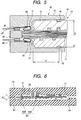
electronic circuit device 10 with reference to FIG. 6 and FIG. 7. First, the O-ring 17 is wrapped around the base portion of theconvex connector 12 of thecircuit board 11 mounted with electronic components. Next, thecircuit board 11 is sandwiched between twomolds - The
cavity 63 formed between the two molds comprises afirst portion 63A corresponding to the exterior shape of the resin-moldedportion 15 and asecond portion 63B in which theconvex connector 12 is placed. Thesecond portion 63B is larger than the outer dimensions of theconvex connector 12 so that theconvex connector 12 will not be brought into contact with the inner walls of the molds. The O-ring 17 is disposed at the entrance to thesecond portion 63B. - When the resin is injected into the
cavity 63 through aresin injection portion 64, the resin is guided to thefirst portion 63A, but the O-ring 17 prevents it from entering thesecond portion 63B. - In this example, the above-mentioned use of the O-
ring 17 prevents resin from being applied to the metal terminals for connection of theconvex connector 12. Thus, theconvex connector 12 exposed from the resin-moldedportion 15 can be formed as illustrated in FIG. 1. If the O-ring is not used, thesecond portion 63B of thecavity 63 must be so constructed that it has the same shape as the outside shape of theconvex connector 12. More specific description will be given. Themolds convex connector 12, and thus resin is prevented from being applied to the metal terminals for connection of theconvex connector 12. However, if themolds convex connector 12, problems arise: there is the possibility that the metal terminals for connection are damaged, and the molds must be fabricated with high accuracy. - The 0-
ring 17 is used when the resin-moldedportion 15 is formed, and is unnecessary when the finishedelectronic circuit device 10 is used. When theelectronic circuit device 10 is in use, the O-ring 17 is disposed in the waterproofed enclosed space as illustrated in FIG. 1. Therefore, the O-ring 17 need not be provided with water resistance, and further need not be provided with oil resistance, resistance to chemicals, heat resistance, vibration resistance, and the like. As a result, a very inexpensive material can be selected. -
Projections 65 are formed on the inner surfaces of themolds projection 65 is formed throughout the inner circumferential surface of thecavity 63. A groove for housing the sealingmember 16 is formed throughout the circumference of the resin-moldedportion 15 by thisprojection 65. - FIG. 7 is a sectional view of the
circuit board 11 placed in thecavity 63 between the two molds as viewed from the direction of arrow A of FIG. 6. When thecircuit board 11 wrapped with the O-ring 17 is sandwiched between the twomolds ring 17 is brought into contact with an end of thesecond portion 63B of thecavity 63. As a result, it can be broken. If the 0-ring 17 is broken, its sealing function does not work, which result in the entry of resin into the second portion of thecavity 63. - The following measure illustrated in FIG. 7 is effective in avoiding this: the areas of the
second portion 63B of thecavity 63 with which areas the O-ring 17 is to be brought into contact are provided beforehand with a clearance angle θ. - With reference to FIG. 6 and FIG. 7, description has been given to a production method for an
electronic circuit device 10 provided on one side with aconvex connector 12. Where anelectronic circuit device 10 with aconvex connector 12 provided on two, three, or four sides is produced, the following measures must be taken: the molds are provided with a shape corresponding to a plurality of theconvex connectors 12 and accordingly requiredresin injection portions 64. - FIG. 8 illustrates a second example of an electronic circuit device of the present invention. In this example, a
projection 18 is provided on the outer surface of the resin-moldedportion 15 of theelectronic circuit device 10. Thehousing 41 of aconcave connector 40 is provided with apivot 50 and alever 51. Theconvex connector 12 of theelectronic circuit device 10 is inserted into the concave portion of the housing of theconcave connector 40. Thereafter, thelever 51 is pivoted about thepivot 50 to engage it with theprojection 18. As a result, theconvex connector 12 of theelectronic circuit device 10 is locked on theconcave connector 40 with reliability. - In this example, when the
projection 18 on the electronic circuit device is engaged with thelever 51 of theconcave connector 40, theelectronic circuit device 10 is prevented from being displaced in the axial direction. Therefore, theelectronic circuit device 10 is prevented from coming off. In addition, theconvex connector 12 need not be abutted against the receivingmember 46 of theconcave connector 40. Therefore, theconvex connector 12 does not receive strong pressing force from the receivingmember 46. Furthermore, theelectronic circuit device 10 is prevented from wobbling to the left and right. This prevents wear and breakage due to pinching force, vibration, or the like that are likely to occur in the following areas: the area of contact between themetal terminals convex connector 12 and themetal terminals concave connector 40; and the area of connection between the sealingmember 16 and the housing of theconcave connector 40. - In the example in FIG. 8, one
lever 51 is provided. Instead, a lever may be provided in two places on the upper and lower sides or on the left and right sides. - The
projection 18 may be formed of the same material as that of the resin-moldedportion 15 as part of the resin-moldedportion 15. More specific description will be given. The molds are provided with concave portion corresponding to the outside shape of theprojection 18. Thus, the projection can be formed simultaneously with the resin-moldedportion 15. If the resin-moldedportion 15 is formed of a material, such as epoxy resin, weak against shear stress, the sectional area of the projection may be increased. Or, a metal piece may be resin-molded therein. - FIG. 9 illustrates a third example of an electronic circuit device of the present invention. In this example, a
recess 19A is formed in the outer surface of the resin-moldedportion 15 of theelectronic circuit device 10. Thehousing 41 of aconcave connector 40 is provided with aprotruded plate 52, and ahook 53 is provided at its end. When theconvex connector 12 of theelectronic circuit device 10 is inserted into the concave portion of the housing of theconcave connector 40, thehook 53 is engaged with therecess 19A. As a result, theconvex connector 12 of the electronic circuit device is locked in theconcave connector 40 with reliability. To remove theconvex connector 12 from theconcave connector 40, one end of thehook 53 only has to be pushed. The other end of thehook 53 is moved by the principle of leverage in the opposite direction to the direction in which thehook 53 is pushed, and it goes out of therecess 19A. - In the example in FIG. 9, one
hook 53 is provided. Instead, a hook may be provided in two places on the upper and lower sides or on the left and right sides. - In this example, when the
electronic circuit device 10 is inserted into theconcave connector 40, thehook 53 is automatically engaged with therecess 19A. Therefore, the following advantage is brought: a human error that can occur in the example illustrated in FIG. 8 involving use of alever 51, that is, forgetting about fixing the circuit board device is prevented. - In this example, the
hook 53 is abutted against therecess 19A in the resin-moldedportion 15. Therefore, while pressing force is applied to therecess 19A in the resin-molded portion, shear stress is not exerted. Unlike the second example in FIG. 8, therefore, it is unnecessary to provide a metal piece or the like in the hook so that it can withstand shear stress. The material of the resin-moldedportion 15 and thehook 53 of theconcave connector 40 can be selected from among a wide range of materials. - FIG. 10 illustrates a fourth example of an electronic circuit device of the present invention. In this example, the
convex connector 12 of theelectronic circuit device 10 includes metal pins 21. The metal pins 21 are substantially in L shape, and one end of them are protruded from theelectronic circuit device 10 and form metal terminals for connection. The other ends are inserted into holes in thecircuit board 11 so that they penetrate the circuit board. In this example, therefore, the metal terminals for connection are disposed on one side plane of theelectronic circuit device 10 including thecircuit board 11. - In the first example illustrated in FIG. 1, part of the
circuit board 11 is exposed from the resin-moldedportion 15. In this example, meanwhile, the whole of thecircuit board 11 is covered with the resin-moldedportion 15. A holdingplate 22 is attached to an end of the resin-moldedportion 15, and the holdingplate 22 is connected with an aligningplate 23. The aligningplate 23 has convex portions, and the ends of the convex portions are abutted against the front face of thecircuit board 11. The metal pins 21 penetrate the holdingplate 22, and they are thereby supported and fixed. - In the example in FIG. 10, two
metal pins 21 are provided. Instead, one metal pin may be provided, or three or more metal pins may be provided. - If a plurality of
metal pins 21 are provided, they can be disposed in a line in parallel with the end face of thecircuit board 11. Instead, they may be disposed in two or more lines. - Description will be given to a production method for the electronic circuit device in this example. First, the holding
plate 22 provided with the metal pins 21 and aligningplate 23 is prepared. The aligningplate 23 may be formed integrally with the holdingplate 22, that is, the aligning plate may be formed of the same material as that of the holding plate. The metal pins 21 may be formed integrally with the holdingplate 22 by insert molding. Instead, the following method may be adopted: holes are formed in the holdingplate 22 and the aligningplate 23, and the metal pins are inserted and fixed therein. Next, thecircuit board 11 and the holdingplate 22 are assembled together. The metal pins 21 are inserted into the holes in thecircuit board 11, and the end of the aligningplate 23 is abutted against the front face of thecircuit board 11. The metal pins 21 and the wires on thecircuit board 11 are connected together by soldering. Thus, the holdingplate 22 having the metal pins 21 is assembled to thecircuit board 11. - The aligning
plate 23 is provided with a function of positioning the holdingplate 22 relative to thecircuit board 11. The accuracy of positioning the metal pins 21 in thecircuit board 11 can be enhanced by this function. - The thus obtained assembly is sandwiched between two molds, and the cavity formed between the molds is filled with resin. In this example, it is unnecessary to use the 0-ring used in the example illustrated in FIG. 1.
- FIG. 11 illustrates a fifth example of an electronic circuit device of the present invention. In this example, the
convex connector 12 of the electronic circuit device includes metal pins 24. The metal pins 24 are substantially in L shape, and one ends of them are protruded from the electronic circuit device and form metal terminals for connection. The other ends are bent into L shape, and connected to themetal wirings circuit board 11. That is, the inner ends of the metal pins 24 are face-mounted on thecircuit board 11. In this example, the metal terminals for connection are symmetrically disposed on the side plane of theelectronic circuit device 10 including thecircuit board 11. - Description will be given to a production method for the electronic circuit device in this example. First, the holding
plate 22 provided with the metal pins 24 is prepared. The metal pins 24 may be formed integrally with the holdingplate 22 by insert molding. Instead, the following method may be adopted: holes are formed in the holdingplate 22, and the metal pins are inserted and fixed therein. Next, thecircuit board 11 and the holdingplate 22 are assembled together. The end of thecircuit board 11 is inserted into between the inner ends of the two metal pins 24. The metal pins 24 and themetal wirings circuit board 11 are connected together by soldering. Since the inner ends of the metal pins 24 are pressed against thecircuit board 11 by spring force from the metal pins 24, soldering of the metal pins 24 may be omitted. Thus, the holdingplate 22 having the metal pins is assembled. - Subsequently, the thus obtained assembly is sandwiched between two molds, and the cavity formed between the molds is filled with resin. In this example, it is unnecessary to use the O-ring used in the example illustrated in FIG. 1.
- In this example, the
circuit board 11 is sandwiched between the inner ends of the metal pins positioned on both sides. Therefore, an even number of metal pins are provided. In this example, it is unnecessary to use the aligning plate in the example illustrated in FIG. 10. - Description will be given to a sixth example of an electronic circuit device of the present invention with reference to FIG. 12 and FIG. 13. FIG. 12 is an enlarged sectional view of an end of the electronic circuit device in this example. FIG. 13 is an enlarged sectional view of the electronic circuit device in this example as a front view.
- As in the first example in FIG. 1, the
convex connector 12 of the electronic circuit device in this example is formed by extending thecircuit board 11. Thecircuit board 11 usually has a laminated structure comprising a plurality of layers, and metal wirings are formed not only on the surfaces but also in internal layers of the board. A plurality of these metal wirings formed in different layers are electrically connected together through throughholes 25. - In this example,
metal terminals convex connector 12 at theend 12A of theconvex connector 12. Meanwhile, themetal terminals internal layers 26 of theconvex connector 12 at theroot portion 12B of theconvex connector 12. Themetal terminals end 12A of theconvex connector 12 are electrically connected with themetal terminals root portion 12B through the through holes 25. - Description will be given to a resin molding method for the electronic circuit device in this example. The
circuit board 11 mounted with electronic components is sandwiched between two molds. The ends of the molds sandwich thebase portion 12B of theconvex connector 12 from both sides. At thebase portion 12B of theconvex connector 12, the metal terminals for connection are formed in internal layers. Therefore, if the ends of the molds are brought into contact with the outer surface of theconvex connector 12, the metal terminals for connection are not damaged or broken. In this example, it is unnecessary to use the O-ring used in the example illustrated in FIG. 1. - It is preferable that the area of contact between the molds and the
circuit board 11 should be widened as much as possible and the contact faces of the upper and lower molds should be symmetrically structured. Thus, stress exerted on thecircuit board 11 is reduced. Further, even if there is warpage in thecircuit board 11, pressing force can be uniformly applied so that the warpage will be eliminated. - Thermosetting resin is poured into the cavity formed between the two molds. The cavity has a shape corresponding to the outside shape of the resin-molded portion. Therefore, it is unnecessary to provide the
first portion 63A as illustrated in FIG. 6. - In considerable cases, only through
holes 25 that penetrate thecircuit board 11 are obtained from the viewpoint of cost and standardization. If through holes 25 are provided between theend 12A and thebase portion 12B of theconvex connector 12, a problem arises. Themetal wirings end 12A of theconvex connector 12 cannot be formed in symmetrical positions as in the example illustrated in FIG. 4. - As illustrated in FIG. 13, the
metal wirings end 12A of theconvex connector 12 are identical in number with each other. However, they are disposed in a staggered configuration on the upper and lower faces. As a result, the following advantage is brought: when theconvex connector 12 is engaged with theconcave connector 40, the pressing forces applied to the upper face and lower face of thecircuit board 11 through the metal terminals for connection become identical. As a result, production of bending stress in thecircuit board 11 is avoided. - FIG. 14 illustrates an electronic circuit device of the present invention with a
protective cover 30 attached over theconvex connector 12. Theprotective cover 30 comprises aframe member 31 and beam-like projections 32, and hooks 33 are provided at the ends of theframe member 31.Recesses 19B are formed in the outer surface of the resin-moldedportion 15 of the electronic circuit device. When theconvex connector 12 of theelectronic circuit device 10 is inserted into theprotective cover 30, the following takes place: the beam-like projections 32 are abutted against an end of the resin-moldedportion 15, and theelectronic circuit device 10 cannot be further pushed in. Thus, the end of theconvex connector 12 is prevented from being abutted against theprotective cover 30. At this time, thehooks 33 are engaged with therecesses 19B. As a result, theprotective cover 30 is fixed on theelectronic circuit device 10 with reliability. To remove theprotective cover 30, thehooks 33 are bent outward, and then theprotective cover 30 is pulled. - The
protective cover 30 is usedwhen theelectronic circuit device 10 is transported and stored. It is unnecessary when theelectronic circuit device 10 is actually installed in an automobile, a motorcycle, an agricultural machine, an industrial machine, a shipboard machine, or the like. Therefore, theprotective cover 30 does not need such a high reliability as theelectronic circuit device 10 needs. It may be formed of PET used for beverages and the like or an inexpensive material corresponding thereto. However, an appropriate material must be selected so that the attachedprotective cover 30 will not come off from theelectronic circuit device 10 due to moisture absorption, thermal deformation, or the like. - FIG. 15 illustrates an example of the construction of a
concave connector 40 used for the electronic circuit device of the present invention. Thehousing 41 of theconcave connector 40 has an attachingportion 55, and the attachingportion 55 is provided withholes 56. When thisconcave connector 40 is attached to astructure 70, such as automobile, motorcycle, agricultural machine, industrial machine, shipboard machine, or the like, the following procedure can be taken: screw holes 71 are formed in thestructure 70, and screws 72 are engaged with the screw holes 71 in thestructure 70 through theholes 56. - In addition to the method in which the
screws 72 are used, various methods can be used to attach and fix theconcave connector 40 to thestructure 70. However, the method in which thescrews 72 are used is preferable in terms of reliability and cost. - With the method in this example, the
electronic circuit device 10 and theconcave connector 40 are fixed as a single-piece construction on thestructure 70. The resonance frequency of the single-piece construction comprising theelectronic circuit device 10 and theconcave connector 40 is lower than the resonance frequency of theelectronic circuit device 10. When it is actually used, therefore, there is the possibility that vibration equivalent to the resonance frequency is applied. In such a case, theelectronic circuit device 10 or theconcave connector 40 is provided with a beam structure, the thickness is increased and the length is reduced, or the like measures are taken. Thus, the resonance frequency is increased, and a construction resistant to stress due to vibration can be obtained. - By providing resistance to vibration as mentioned above, it is made possible to install the
electronic circuit device 10 and theconcave connector 40 in this example on a structure, such as automobile, motorcycle, agricultural machine, industrial machine, shipboard machine, or the like. As a result, installation workability and maintenance workability can be enhanced. - FIG. 16 illustrates the construction of another example of a
concave connector 40 used for the electronic circuit device of the present invention. Theconcave connector 40 in this example has threeconcave portions housing 41. The first and secondconcave portions concave portion 42 of theconcave connector 40 illustrated in FIG. 5.Metal wirings 49 are provided in thehousing 41. One ends of themetal wirings 49 are connected with the metal terminals for connection disposed on the bottom of the first and secondconcave portions terminals 49A protruded on the bottom of the thirdconcave portion 42C. The terminals of the thirdconcave portion 42C form convex connectors. - To install the concave connector in this example in a
structure 70, such as automobile, motorcycle, agricultural machine, industrial machine, shipboard machine, or the like, screws 72 are used as in the example in FIG. 15. The example illustrated in FIG. 16 is provided with two concave portions, that is, slots so that two electronic circuit devices can be attached thereto. Instead, two or more slots may be provided like PCI slots in personal computers. - A plurality of
electronic circuit devices electronic circuit device 10A is mounted with computing function elements with a microcomputer at the nucleus; and the secondelectronic circuit device 10B is mounted with semiconductor devices, such as FET, for controlling large currents. - With the concave connector in this example, functions provided for the following can be easily changed by replacing the
electronic circuit devices electronic circuit devices - In addition, if the necessity for enhancing the functions of a control circuit arises in the future, that can be coped with by replacing only the required electronic circuit devices as needed. If a problem arises with respect to the functions of a specific control circuit, it can also be solved by taking the same measure.
- The metal wirings 49 of the concave connector can also be provided with a desired control circuit , an arithmetic circuit, or the like. In this case, it is possible to replace only the concave connector without changing the
electronic circuit devices electronic circuit devices - The electronic circuit device and concave connector according to the present invention can be used for automobiles, motorcycles, agricultural machines, industrial machines, shipboard machines; and the like. Where the present invention is used for an automobile, it is applicable to control modules such as engine control module, motor control module, and automatic shift control module, and sensor modules such as pressure sensor module and air flow meter module. This makes it possible to easily attain the effects of the enhancement of productivity of these modules and reduction of their size and cost.
- Further, the present invention is applicable to the following items: brake control module that provides active safety function expected to evolve in the future; control modules such as suspension control module, steering control module, air bag control module, and seat belt control module; measurement modules such as following distance measurement module; and communication modules for information exchange with the outside of the vehicle via radio waves for obtaining the functions of ITS and the like, such as cellular phone communication module, ETC communication module, GPS communication module, and VICS communication module. The electronic circuit device and concave connector according to the present invention is excellent in resistance to chemicals. This makes it possible to enhance the degree of freedom in mounting control modules for equipment utilizing chemical change, such as fuel battery control module and lithium ion battery charge/discharge control module.
- Up to this point, description has been given to examples of the present invention. However, the present invention is not limited to the above-described examples, and it will be understood by those skilled in the art that various changes may be resorted to within the scope of the invention described in the claims.
Claims (18)
- An electronic circuit device (10) comprising: a circuit board (11) mounting an electronic component; a resin-molded portion (15) formed of resin for covering the electronic component; a convex connector (12) that has a metal terminal for connection and is exposed from the resin-molded portion; and a sealing member (16) wrapped around the resin-molded portion.
- The electronic circuit device according to Claim 1, wherein the convex connector is formed as an extended portion of the circuit board.
- The electronic circuit device according to Claim 2, wherein a metal terminal (13, 14) for connection is formed as an extended portion of metal wiring (117, 118) formed on the circuit board.
- The electronic circuit device according to Claim 2, wherein a metal terminal (13, 14) for connection is symmetrically formed on both sides of the convex connector.
- The electronic circuit device according to Claim 2, wherein a metal terminal (13, 14) for connection is formed only at an end of the convex connector and the metal wiring (117,118) connected with the metal terminal for connection is disposed in internal layers in the circuit board at the base of the convex connector.
- The electronic circuit device according to Claim 2, wherein when the width of the resin-molded portion is D and the distance between the end of the resin-molded portion on the side where the convex connector is formed and the sealing member is H, H is approximately twice D.
- The electronic circuit device according to Claim 1, wherein a cover (30) that covers the convex connector is provided and the cover has a hook (33) to be engaged with concave portions (19B) formed in the resin-molded portion.
- The electronic circuit device according to Claim 1, wherein the convex connector has a metal pin (21, 24), and one end of the metal pin is exposed from the resin-molded portion and the other end of the metal pin is connected with the metal wiring of the circuit board.
- The electronic circuit device according to Claim 8, wherein a holding plate (22) is provided at an end of the resin-molded portion, and the metal pin is held by the holding plate.
- A connecting structure for electronic circuit device comprising: an electronic circuit device (10), which comprises a circuit board (11) mounted with electronic components, a resin-molded portion (15) formed of resin so disposed that the electronic components are covered therewith, a convex connector (12) that has metal terminals for connection and is exposed from the resin-molded portion, and a sealing member (16) wrapped around the resin-molded portion; and a concave connector (40) having a housing (41), a concave portion (42) formed in the housing, and metal terminals (44, 45) for connection formed on the bottom of the concave portion, whereby when the convex connector is inserted into the concave portion of the concave connector so that the metal terminals for connection of the convex connector are brought into contact with the metal terminals for connection of the concave connector, the sealing member is pressed against the wall portion of the concave portion of the housing and the contact area between the two of metal terminals for connection are sealed from the outside.
- The connecting structure for electronic circuit device according to Claim 10, wherein a convex portion (18) is formed on the resin-molded portion of the electronic circuit device, the housing of the concave connector is provided with a pivot (50) and a lever (51) rotatable on the pivot, and the connecting structure is so constructed that, when the convex connector is inserted into the concave portion of the concave connector, the lever can be engaged with the convex portion.
- The connecting structure for electronic circuit device according to Claim 10, wherein the resin-molded portion of the electronic circuit device is provided with a concave portion (19A), the housing of the concave connector is provided with a hook (53) and the connecting structure is so constructed that, when the convex connector is inserted into the concave portion of the concave connector, the hook can be engaged with the concave portion.
- The connecting structure for electronic circuit device according to Claim 10, wherein the concave connector has a plurality of the concave portion, and the connecting structure is so constructed that a plurality of the convex connector can be inserted into the concave portion of the concave connector.
- The connecting structure for electronic circuit device according to Claim 13, wherein the concave portion is provided with protruded metal terminals for connection, and the housing of the concave connector has a metal wiring that connects the metal terminals for connection disposed on the bottom of the concave portion with the metal terminal for connection protruded from the concave portion.
- A production method for an electronic circuit device comprising: a circuit board mounted with electronic components; a resin-molded portion formed of resin so constructed that the electronic components are covered therewith; a convex connector that has metal terminals for connection and is exposed from the resin-molded portion; and a sealing member wrapped around the resin-molded portion, the production method comprising the steps of:preparing a circuit board that has a convex connector at an end thereof and is mounted on the surface thereof with electronic components;preparing two molds so as to form a cavity comprising a first portion corresponding to the outside shape of the resin-molded portion and a second portion in which the convex connector is disposed;sandwiching the circuit board between the two molds; andinjecting resin into the cavity through a resin injection portion formed between the two molds.
- The production method for the electronic circuit device according to Claim 15, which further comprises the step of wrapping an O-ring around the base portion of the convex connector.
- The production method for the electronic circuit device according to Claim 15, wherein a clearance angle is formed in the inner wall of the second portion of the cavity with which the 0-ring is in contact so that, when the circuit board is sandwiched between the two molds, the 0-ring will not be caught between the edges of the two molds.
- The production method for the electronic circuit device according to Claim 15, wherein the metal terminal for connection is formed only at an end of the convex connector and the metal wiring connected with the metal terminal for connection are disposed in internal layers in the circuit board at the base of the convex connector.
Applications Claiming Priority (1)
| Application Number | Priority Date | Filing Date | Title |
|---|---|---|---|
| JP2004364824A JP4478007B2 (en) | 2004-12-16 | 2004-12-16 | Electronic circuit device and manufacturing method thereof |
Publications (2)
| Publication Number | Publication Date |
|---|---|
| EP1672972A1 true EP1672972A1 (en) | 2006-06-21 |
| EP1672972B1 EP1672972B1 (en) | 2010-05-19 |
Family
ID=35929849
Family Applications (1)
| Application Number | Title | Priority Date | Filing Date |
|---|---|---|---|
| EP05017765A Active EP1672972B1 (en) | 2004-12-16 | 2005-08-16 | Electronic circuit device and production method of the same |
Country Status (5)
| Country | Link |
|---|---|
| US (2) | US7514784B2 (en) |
| EP (1) | EP1672972B1 (en) |
| JP (1) | JP4478007B2 (en) |
| CN (2) | CN100407387C (en) |
| DE (1) | DE602005021303D1 (en) |
Cited By (18)
| Publication number | Priority date | Publication date | Assignee | Title |
|---|---|---|---|---|
| EP2053907A3 (en) * | 2007-10-26 | 2009-07-15 | Delphi Technologies, Inc. | Method of producing an overmolded electronic module with a flexible circuit pigtail |
| EP2107641A1 (en) * | 2007-01-25 | 2009-10-07 | Nippon Sheet Glass Company Limited | Terminal sealing apparatus |
| EP2043413A3 (en) * | 2007-09-28 | 2010-07-28 | Delphi Technologies, Inc. | Method of overmolding an electronic assembly having an insert-moled vertical mount connector header |
| US20110120073A1 (en) * | 2009-05-18 | 2011-05-26 | Ron Flanary | Water-Resistant Electric Motor |
| WO2011113645A1 (en) * | 2010-03-17 | 2011-09-22 | Robert Bosch Gmbh | Control device |
| WO2012123226A3 (en) * | 2011-03-11 | 2013-04-04 | Robert Bosch Gmbh | Component, in particular as a constituent part of a switchgear or control device |
| WO2013056956A1 (en) * | 2011-10-18 | 2013-04-25 | Robert Bosch Gmbh | Control unit for a motor vehicle having a connector housing |
| CN103097775A (en) * | 2010-09-09 | 2013-05-08 | 株式会社自动网络技术研究所 | Electronic circuit unit to be mounted on automatic transmission for vehicle, and method of manufacturing thereof |
| CN103250477A (en) * | 2010-12-08 | 2013-08-14 | 罗伯特·博世有限公司 | Electrical circuit arrangement and method for producing an electrical circuit arrangement |
| EP2695717A1 (en) * | 2012-08-07 | 2014-02-12 | Hosiden Corporation | Device module and method of manufacturing the device module |
| EP2695715A1 (en) * | 2012-08-07 | 2014-02-12 | Hosiden Corporation | Device module and method of manufacturing the same |
| WO2015010844A2 (en) * | 2013-07-26 | 2015-01-29 | Robert Bosch Gmbh | Connecting assembly between a control device and a module connected to the control device |
| WO2015014541A3 (en) * | 2013-07-29 | 2015-04-02 | Robert Bosch Gmbh | Control device and assembly having a control device |
| WO2016008672A1 (en) * | 2014-07-18 | 2016-01-21 | Zf Friedrichshafen Ag | Electronic transmission controller, and method for producing same |
| EP3288351A1 (en) * | 2016-08-22 | 2018-02-28 | Woodward, Inc. | Frame for printed circuit board support in high vibration |
| WO2017207795A3 (en) * | 2016-06-03 | 2018-03-01 | Continental Teves Ag & Co. Ohg | Sensor, method and sensor arrangement |
| WO2018108364A1 (en) * | 2016-12-13 | 2018-06-21 | Robert Bosch Gmbh | Transmission control device, in particular for a motor vehicle, and method for producing an electrical-connector housing |
| EP3869551A4 (en) * | 2018-11-23 | 2021-12-29 | Huawei Technologies Co., Ltd. | Encapsulation module based on pins of pcb body and preparation method therefor |
Families Citing this family (52)
| Publication number | Priority date | Publication date | Assignee | Title |
|---|---|---|---|---|
| JP2006032490A (en) * | 2004-07-13 | 2006-02-02 | Hitachi Ltd | Engine controlling circuit device |
| US20070279877A1 (en) * | 2006-05-30 | 2007-12-06 | Stephan Dobritz | Circuit board arrangement |
| DE102006038373A1 (en) * | 2006-08-12 | 2008-02-14 | Robert Bosch Gmbh | Electrical device, especially for determining electrical parameters, e.g. battery sensor, has conductive boundary surface between two conductor sections that is offset relative to the central axis |
| JP4942452B2 (en) * | 2006-10-31 | 2012-05-30 | 三洋電機株式会社 | Circuit equipment |
| JP4958526B2 (en) * | 2006-11-30 | 2012-06-20 | 三洋電機株式会社 | Circuit device and circuit module |
| WO2008111524A1 (en) * | 2007-03-09 | 2008-09-18 | Omron Corporation | Package manufacturing method, package, optical module and die for integral molding |
| JP4860552B2 (en) * | 2007-06-08 | 2012-01-25 | 日本オプネクスト株式会社 | Semiconductor device |
| WO2009069542A1 (en) * | 2007-11-29 | 2009-06-04 | Ngk Spark Plug Co., Ltd. | Metal-resin compound member |
| JP4483960B2 (en) * | 2008-03-19 | 2010-06-16 | 株式会社デンソー | Electronic equipment |
| US20100254109A1 (en) | 2009-03-19 | 2010-10-07 | Olympus Corporation | Mount assembly and method for manufacturing mount assembly |
| JP5110049B2 (en) * | 2009-07-16 | 2012-12-26 | 株式会社デンソー | Electronic control device |
| JP2011100718A (en) * | 2009-10-05 | 2011-05-19 | Yazaki Corp | Connector |
| DE102010002950A1 (en) | 2010-03-17 | 2011-09-22 | Robert Bosch Gmbh | CIRCUIT ARRANGEMENT AND ASSOCIATED CONTROL UNIT FOR A MOTOR VEHICLE |
| DE102010002945A1 (en) | 2010-03-17 | 2011-09-22 | Robert Bosch Gmbh | CIRCUIT ARRANGEMENT AND ASSOCIATED CONTROL UNIT FOR A MOTOR VEHICLE |
| DE102010048768A1 (en) * | 2010-10-15 | 2012-04-19 | Fraunhofer-Gesellschaft zur Förderung der angewandten Forschung e.V. | Sensor system for implanting in a body |
| JP2012186371A (en) * | 2011-03-07 | 2012-09-27 | Taiyo Yuden Co Ltd | Method of manufacturing electronic circuit device |
| CN102883583B (en) * | 2011-03-11 | 2016-08-17 | 马维尔以色列(M.I.S.L.)有限公司 | Heat dissipation type high power system |
| TW201241603A (en) * | 2011-04-08 | 2012-10-16 | Asustek Comp Inc | Motherboard |
| JP5449249B2 (en) * | 2011-04-26 | 2014-03-19 | 三菱電機株式会社 | Electronic control unit |
| JP5441956B2 (en) * | 2011-05-26 | 2014-03-12 | 三菱電機株式会社 | Resin-sealed electronic control device and manufacturing method thereof |
| US8730675B2 (en) * | 2011-08-25 | 2014-05-20 | Sony Corporation | Electronic device and method of radiating heat from electronic device |
| US9030842B2 (en) | 2011-09-23 | 2015-05-12 | Electrojet, Inc. | Sealed overmolded circuit board with sensor seal and edge connector seal and production method of the same |
| DE102011088037A1 (en) * | 2011-12-08 | 2013-06-13 | Robert Bosch Gmbh | Arrangement of an electronic module between the gear compartment and engine compartment |
| DE102012201177A1 (en) * | 2012-01-27 | 2013-08-01 | Robert Bosch Gmbh | Plastic-sheathed component carrier for use in electronic powertrain mold device in motor car, has vias filled with covering region with mold compound such that connection is formed between mold layers above and below board, respectively |
| DE102012204630A1 (en) | 2012-03-22 | 2013-09-26 | Robert Bosch Gmbh | Control device for controlling thermoplastic molding, during manufacturing of e.g. chip, has substrate and electronic component enclosed by mold where device is surrounded by cover over sealing region that is overlapped in exposed region |
| JP2013232312A (en) | 2012-04-27 | 2013-11-14 | Jst Mfg Co Ltd | Card member, card edge connector, and manufacturing method of card member |
| DE102012207877A1 (en) * | 2012-05-11 | 2013-11-14 | Robert Bosch Gmbh | Module for a prefabricated connection strip and method for producing prefabricated connection strips |
| US9425574B2 (en) * | 2012-05-11 | 2016-08-23 | Tpc Wire & Cable Corp. | Cast forming methods for making sealed conductors |
| JP6257881B2 (en) * | 2012-05-31 | 2018-01-10 | 株式会社ミクニ | Engine control unit |
| JP2013251414A (en) * | 2012-05-31 | 2013-12-12 | Mikuni Corp | Engine control unit |
| DE102012215673A1 (en) * | 2012-09-04 | 2014-03-06 | Zf Friedrichshafen Ag | Arrangement of an electrical control unit to a circuit board |
| KR101561996B1 (en) * | 2012-09-14 | 2015-10-20 | 현대모비스 주식회사 | card key for vehicle |
| US9713260B2 (en) | 2013-02-08 | 2017-07-18 | Keihin Corporation | Electronic circuit device and method for manufacturing same |
| DE102013002629A1 (en) * | 2013-02-15 | 2014-08-21 | HKR Seuffer Automotive GmbH & Co. KG | Cover element and housing device for use of the cover element |
| DE102013212446A1 (en) * | 2013-06-27 | 2015-01-15 | Zf Friedrichshafen Ag | Electric circuit and method for producing an electrical circuit for driving a load |
| JP6219092B2 (en) * | 2013-08-06 | 2017-10-25 | 本田技研工業株式会社 | Electrical component arrangement structure |
| DE102014216518A1 (en) * | 2014-08-20 | 2016-02-25 | Robert Bosch Gmbh | Electronic control unit and mold and method for manufacturing an electronic control unit |
| WO2016084537A1 (en) * | 2014-11-25 | 2016-06-02 | 日立オートモティブシステムズ株式会社 | Electronic control device |
| DE102015209191A1 (en) * | 2015-02-10 | 2016-08-11 | Conti Temic Microelectronic Gmbh | Mechatronic component and method for its production |
| DE102015112337A1 (en) * | 2015-07-29 | 2017-02-02 | Bühler Motor GmbH | Circuit board assembly, oil pump with such a printed circuit board assembly, use of the printed circuit board assembly and manufacturing method |
| KR101756847B1 (en) | 2016-09-27 | 2017-07-12 | 한국기계연구원 | Wearable patch type hybrid substrate and a method for fabricating the same |
| KR101855943B1 (en) | 2017-02-21 | 2018-05-10 | 한국기계연구원 | Wearable patch type hybrid substrate and a method for fabricating the same |
| JP6966259B2 (en) * | 2017-08-25 | 2021-11-10 | 日立Astemo株式会社 | Resin-sealed in-vehicle electronic control device |
| JP2019102485A (en) * | 2017-11-28 | 2019-06-24 | 株式会社村田製作所 | Electronic apparatus |
| DE102018218967A1 (en) * | 2018-04-25 | 2019-10-31 | Mitsubishi Electric Corporation | Electronic device unit |
| JP7079163B2 (en) * | 2018-07-05 | 2022-06-01 | 日立Astemo株式会社 | Electronic control device |
| JP7232582B2 (en) * | 2018-07-05 | 2023-03-03 | 日立Astemo株式会社 | Resin-encapsulated in-vehicle electronic control unit |
| JP7049957B2 (en) * | 2018-08-01 | 2022-04-07 | 日立Astemo株式会社 | Manufacturing method of electronic control device |
| JP7037870B2 (en) * | 2018-08-01 | 2022-03-17 | 日立Astemo株式会社 | Electronic control device |
| JP6945513B2 (en) | 2018-09-20 | 2021-10-06 | 日立Astemo株式会社 | Electronic control device |
| JPWO2020066054A1 (en) * | 2018-09-27 | 2020-04-02 | ||
| DE102018220012A1 (en) * | 2018-11-22 | 2020-05-28 | Zf Friedrichshafen Ag | Printed circuit board, overmolding tool and method for overmolding a printed circuit board |
Citations (4)
| Publication number | Priority date | Publication date | Assignee | Title |
|---|---|---|---|---|
| US5909915A (en) * | 1993-07-05 | 1999-06-08 | Mitsubishi Denki Kabushiki Kaisha | Resin-molded electronic circuit device |
| JP2002321247A (en) * | 2001-04-24 | 2002-11-05 | Matsushita Electric Works Ltd | Manufacturing method for memory card |
| DE20319173U1 (en) * | 2003-12-10 | 2004-03-11 | Kingpak Technology Inc., Chupei | Small memory card |
| EP1487246A1 (en) * | 2003-06-06 | 2004-12-15 | HONDA MOTOR CO., Ltd. | Resin encapsulated electronic component unit and method of manufacturing the same |
Family Cites Families (17)
| Publication number | Priority date | Publication date | Assignee | Title |
|---|---|---|---|---|
| US2761111A (en) * | 1953-02-16 | 1956-08-28 | Amphenol Electronics Corp | Breakaway connector |
| JPS6022475B2 (en) * | 1980-12-29 | 1985-06-01 | 富士通株式会社 | Rubbed structure of electrical connection body |
| US5577937A (en) * | 1993-12-27 | 1996-11-26 | Sumitomo Wiring Systems, Ltd. | Method and apparatus for connecting electronic parts and terminals |
| US5510959A (en) * | 1995-05-17 | 1996-04-23 | The Whitaker Corporation | High density PCMCIA frame kit |
| JPH0955459A (en) * | 1995-06-06 | 1997-02-25 | Seiko Epson Corp | Semiconductor device |
| DE19645636C1 (en) * | 1996-11-06 | 1998-03-12 | Telefunken Microelectron | Power module for operating electric motor with speed and power control |
| US6180045B1 (en) * | 1998-05-20 | 2001-01-30 | Delco Electronics Corporation | Method of forming an overmolded electronic assembly |
| CN1426572B (en) * | 2000-11-09 | 2010-05-26 | 索尼公司 | Holder for card-like electronic device |
| EP1317169B1 (en) * | 2001-03-22 | 2012-05-09 | Sony Corporation | Electronic device and information reproducing system |
| JP4801274B2 (en) * | 2001-03-29 | 2011-10-26 | 本田技研工業株式会社 | Control box with built-in pressure sensor |
| TW585015B (en) * | 2001-06-28 | 2004-04-21 | Sanyo Electric Co | Hybrid integrated circuit device and method for manufacturing same |
| JP2003321247A (en) | 2002-05-07 | 2003-11-11 | Nitto Boseki Co Ltd | Glass composition for glass fiber |
| CN1321485C (en) * | 2002-07-08 | 2007-06-13 | 林原 | Connecting device for wire |
| JP3884354B2 (en) | 2002-09-13 | 2007-02-21 | 株式会社日立製作所 | Electrical / electronic module with integrated molded structure of connector and electronic component |
| JP4115228B2 (en) * | 2002-09-27 | 2008-07-09 | 三洋電機株式会社 | Circuit device manufacturing method |
| US7134194B2 (en) * | 2003-11-13 | 2006-11-14 | Delphi Technologies, Inc. | Method of developing an electronic module |
| JP2006032490A (en) * | 2004-07-13 | 2006-02-02 | Hitachi Ltd | Engine controlling circuit device |
-
2004
- 2004-12-16 JP JP2004364824A patent/JP4478007B2/en active Active
-
2005
- 2005-07-29 CN CN2005100884380A patent/CN100407387C/en active Active
- 2005-07-29 CN CN2008101254870A patent/CN101309553B/en active Active
- 2005-08-09 US US11/199,177 patent/US7514784B2/en active Active
- 2005-08-16 EP EP05017765A patent/EP1672972B1/en active Active
- 2005-08-16 DE DE602005021303T patent/DE602005021303D1/en active Active
-
2009
- 2009-01-09 US US12/350,992 patent/US7934312B2/en active Active
Patent Citations (4)
| Publication number | Priority date | Publication date | Assignee | Title |
|---|---|---|---|---|
| US5909915A (en) * | 1993-07-05 | 1999-06-08 | Mitsubishi Denki Kabushiki Kaisha | Resin-molded electronic circuit device |
| JP2002321247A (en) * | 2001-04-24 | 2002-11-05 | Matsushita Electric Works Ltd | Manufacturing method for memory card |
| EP1487246A1 (en) * | 2003-06-06 | 2004-12-15 | HONDA MOTOR CO., Ltd. | Resin encapsulated electronic component unit and method of manufacturing the same |
| DE20319173U1 (en) * | 2003-12-10 | 2004-03-11 | Kingpak Technology Inc., Chupei | Small memory card |
Non-Patent Citations (1)
| Title |
|---|
| PATENT ABSTRACTS OF JAPAN vol. 2003, no. 03 5 May 2003 (2003-05-05) * |
Cited By (36)
| Publication number | Priority date | Publication date | Assignee | Title |
|---|---|---|---|---|
| EP2107641A4 (en) * | 2007-01-25 | 2014-01-01 | Nippon Sheet Glass Co Ltd | Terminal sealing apparatus |
| EP2107641A1 (en) * | 2007-01-25 | 2009-10-07 | Nippon Sheet Glass Company Limited | Terminal sealing apparatus |
| EP2043413A3 (en) * | 2007-09-28 | 2010-07-28 | Delphi Technologies, Inc. | Method of overmolding an electronic assembly having an insert-moled vertical mount connector header |
| US7739791B2 (en) | 2007-10-26 | 2010-06-22 | Delphi Technologies, Inc. | Method of producing an overmolded electronic module with a flexible circuit pigtail |
| EP2053907A3 (en) * | 2007-10-26 | 2009-07-15 | Delphi Technologies, Inc. | Method of producing an overmolded electronic module with a flexible circuit pigtail |
| US20110120073A1 (en) * | 2009-05-18 | 2011-05-26 | Ron Flanary | Water-Resistant Electric Motor |
| US8643231B2 (en) * | 2009-05-18 | 2014-02-04 | Moog Inc. | Water-resistant electric motor |
| WO2011113645A1 (en) * | 2010-03-17 | 2011-09-22 | Robert Bosch Gmbh | Control device |
| CN103097775B (en) * | 2010-09-09 | 2015-06-03 | 株式会社自动网络技术研究所 | Electronic circuit unit to be mounted on automatic transmission for vehicle, and method of manufacturing thereof |
| CN103097775A (en) * | 2010-09-09 | 2013-05-08 | 株式会社自动网络技术研究所 | Electronic circuit unit to be mounted on automatic transmission for vehicle, and method of manufacturing thereof |
| CN103250477A (en) * | 2010-12-08 | 2013-08-14 | 罗伯特·博世有限公司 | Electrical circuit arrangement and method for producing an electrical circuit arrangement |
| CN103250477B (en) * | 2010-12-08 | 2016-02-10 | 罗伯特·博世有限公司 | The method of the circuit unit of electricity and the circuit unit for the manufacture of electricity |
| WO2012123226A3 (en) * | 2011-03-11 | 2013-04-04 | Robert Bosch Gmbh | Component, in particular as a constituent part of a switchgear or control device |
| CN103875131A (en) * | 2011-10-18 | 2014-06-18 | 罗伯特·博世有限公司 | Control unit for a motor vehicle having a connector housing |
| WO2013056956A1 (en) * | 2011-10-18 | 2013-04-25 | Robert Bosch Gmbh | Control unit for a motor vehicle having a connector housing |
| CN103875131B (en) * | 2011-10-18 | 2017-07-14 | 罗伯特·博世有限公司 | The controller for motor vehicle with plug casing |
| EP3045284A1 (en) * | 2012-08-07 | 2016-07-20 | Hosiden Corporation | Device module and method of manufacturing the same |
| EP2695717A1 (en) * | 2012-08-07 | 2014-02-12 | Hosiden Corporation | Device module and method of manufacturing the device module |
| EP2695715A1 (en) * | 2012-08-07 | 2014-02-12 | Hosiden Corporation | Device module and method of manufacturing the same |
| US10154602B2 (en) | 2012-08-07 | 2018-12-11 | Hosiden Corporation | Method of manufacturing a device module |
| US9872409B2 (en) | 2012-08-07 | 2018-01-16 | Hosiden Corporation | Device module and method of manufacturing the same |
| WO2015010844A3 (en) * | 2013-07-26 | 2015-04-09 | Robert Bosch Gmbh | Connecting assembly between a control device and a module connected to the control device |
| WO2015010844A2 (en) * | 2013-07-26 | 2015-01-29 | Robert Bosch Gmbh | Connecting assembly between a control device and a module connected to the control device |
| WO2015014541A3 (en) * | 2013-07-29 | 2015-04-02 | Robert Bosch Gmbh | Control device and assembly having a control device |
| US10440845B2 (en) | 2014-07-18 | 2019-10-08 | Zf Friedrichshafen Ag | Electronic transmission controller, and method for producing same |
| WO2016008672A1 (en) * | 2014-07-18 | 2016-01-21 | Zf Friedrichshafen Ag | Electronic transmission controller, and method for producing same |
| CN109314331A (en) * | 2016-06-03 | 2019-02-05 | 大陆-特韦斯股份有限公司 | Sensor, method and sensor module |
| WO2017207795A3 (en) * | 2016-06-03 | 2018-03-01 | Continental Teves Ag & Co. Ohg | Sensor, method and sensor arrangement |
| US20190139931A1 (en) * | 2016-06-03 | 2019-05-09 | Continental Teves Ag & Co. Ohg | Sensor, method and sensor arrangement |
| US10950574B2 (en) | 2016-06-03 | 2021-03-16 | Continental Teves Ag & Co. Ohg | Sensor having system-in-package module, method for producing the same, and sensor arrangement |
| EP3288351A1 (en) * | 2016-08-22 | 2018-02-28 | Woodward, Inc. | Frame for printed circuit board support in high vibration |
| US10561039B2 (en) | 2016-08-22 | 2020-02-11 | Woodward, Inc. | Frame for printed circuit board support in high vibration |
| WO2018108364A1 (en) * | 2016-12-13 | 2018-06-21 | Robert Bosch Gmbh | Transmission control device, in particular for a motor vehicle, and method for producing an electrical-connector housing |
| US10939565B2 (en) | 2016-12-13 | 2021-03-02 | Robert Bosch Gmbh | Transmission control device, in particular for a motor vehicle, and method for producing an electrical-connector housing |
| EP3869551A4 (en) * | 2018-11-23 | 2021-12-29 | Huawei Technologies Co., Ltd. | Encapsulation module based on pins of pcb body and preparation method therefor |
| US11641072B2 (en) | 2018-11-23 | 2023-05-02 | Huawei Technologies Co., Ltd. | PCB-pinout based packaged module and method for preparing PCB-pinout based packaged module |
Also Published As
| Publication number | Publication date |
|---|---|
| US7514784B2 (en) | 2009-04-07 |
| CN100407387C (en) | 2008-07-30 |
| DE602005021303D1 (en) | 2010-07-01 |
| US7934312B2 (en) | 2011-05-03 |
| EP1672972B1 (en) | 2010-05-19 |
| CN101309553B (en) | 2011-07-20 |
| JP2006173402A (en) | 2006-06-29 |
| CN101309553A (en) | 2008-11-19 |
| US20090119913A1 (en) | 2009-05-14 |
| CN1790649A (en) | 2006-06-21 |
| JP4478007B2 (en) | 2010-06-09 |
| US20060134937A1 (en) | 2006-06-22 |
Similar Documents
| Publication | Publication Date | Title |
|---|---|---|
| EP1672972B1 (en) | Electronic circuit device and production method of the same | |
| EP1677583B1 (en) | Electronic control unit and manufacturing method therefore | |
| EP1806960B1 (en) | Electronic device | |
| US4766520A (en) | Injection molded circuit housing | |
| US7877868B2 (en) | Method of fabricating circuit configuration member | |
| US7294007B1 (en) | Electronics enclosure and method of fabricating an electronics enclosure | |
| US20040095732A1 (en) | Housing structure of vehicle-mounted electronic equipment | |
| US8530759B2 (en) | Electronic apparatus | |
| US6683789B1 (en) | Electronic control module for a removable connector and methods of assembling same | |
| JP6442527B2 (en) | Electronic control unit | |
| CN108476590A (en) | Resin encapsulation type on-vehicle control apparatus | |
| CN108029228A (en) | Electronic control unit | |
| US6892699B2 (en) | Throttle body and air intake equipment for internal combustion engine | |
| CN109479381B (en) | Electronic control device and assembling method thereof | |
| JP3587425B2 (en) | Intake system control device for internal combustion engine | |
| US11910544B2 (en) | Assembly of printed circuit board with overmolded epoxy to baseplate | |
| JP2002285866A (en) | Throttle device and its manufacturing method | |
| JP2014239103A (en) | Electronic control device, electronic control unit, and method of manufacturing electronic control device | |
| US20230352861A1 (en) | Thermal connection between printed circuit board and base plate with epoxy molded material | |
| CN110476490A (en) | Electronic module and transmission control unit for transmission control unit | |
| JP2002252482A (en) | Housing case for circuit board and housing method | |
| KR102015670B1 (en) | Molding wiring board unit | |
| CN116067546A (en) | Electrical device |
Legal Events
| Date | Code | Title | Description |
|---|---|---|---|
| PUAI | Public reference made under article 153(3) epc to a published international application that has entered the european phase |
Free format text: ORIGINAL CODE: 0009012 |
|
| AK | Designated contracting states |
Kind code of ref document: A1 Designated state(s): AT BE BG CH CY CZ DE DK EE ES FI FR GB GR HU IE IS IT LI LT LU LV MC NL PL PT RO SE SI SK TR |
|
| AX | Request for extension of the european patent |
Extension state: AL BA HR MK YU |
|
| 17P | Request for examination filed |
Effective date: 20061221 |
|
| 17Q | First examination report despatched |
Effective date: 20070125 |
|
| AKX | Designation fees paid |
Designated state(s): DE |
|
| RIC1 | Information provided on ipc code assigned before grant |
Ipc: H05K 5/06 20060101ALI20090921BHEP Ipc: H05K 5/00 20060101ALI20090921BHEP Ipc: H05K 3/28 20060101AFI20090921BHEP |
|
| GRAP | Despatch of communication of intention to grant a patent |
Free format text: ORIGINAL CODE: EPIDOSNIGR1 |
|
| GRAS | Grant fee paid |
Free format text: ORIGINAL CODE: EPIDOSNIGR3 |
|
| GRAA | (expected) grant |
Free format text: ORIGINAL CODE: 0009210 |
|
| AK | Designated contracting states |
Kind code of ref document: B1 Designated state(s): DE |
|
| REF | Corresponds to: |
Ref document number: 602005021303 Country of ref document: DE Date of ref document: 20100701 Kind code of ref document: P |
|
| PLBE | No opposition filed within time limit |
Free format text: ORIGINAL CODE: 0009261 |
|
| STAA | Information on the status of an ep patent application or granted ep patent |
Free format text: STATUS: NO OPPOSITION FILED WITHIN TIME LIMIT |
|
| 26N | No opposition filed |
Effective date: 20110222 |
|
| REG | Reference to a national code |
Ref country code: DE Ref legal event code: R097 Ref document number: 602005021303 Country of ref document: DE Effective date: 20110221 |
|
| REG | Reference to a national code |
Ref country code: DE Ref legal event code: R081 Ref document number: 602005021303 Country of ref document: DE Owner name: HITACHI ASTEMO, LTD., HITACHINAKA-SHI, JP Free format text: FORMER OWNER: HITACHI AUTOMOTIVE SYSTEMS, LTD., HITACHINAKA-SHI, IBARAKI, JP Ref country code: DE Ref legal event code: R081 Ref document number: 602005021303 Country of ref document: DE Owner name: HITACHI ASTEMO, LTD., HITACHINAKA-SHI, JP Free format text: FORMER OWNER: HITACHI, LTD., TOKYO, JP |
|
| PGFP | Annual fee paid to national office [announced via postgrant information from national office to epo] |
Ref country code: DE Payment date: 20230627 Year of fee payment: 19 |