EP1677414A1 - Power amplifying apparatus using asymmetric power drive - Google Patents
Power amplifying apparatus using asymmetric power drive Download PDFInfo
- Publication number
- EP1677414A1 EP1677414A1 EP05028410A EP05028410A EP1677414A1 EP 1677414 A1 EP1677414 A1 EP 1677414A1 EP 05028410 A EP05028410 A EP 05028410A EP 05028410 A EP05028410 A EP 05028410A EP 1677414 A1 EP1677414 A1 EP 1677414A1
- Authority
- EP
- European Patent Office
- Prior art keywords
- amplifier
- power
- peaking
- carrier
- amplifying apparatus
- Prior art date
- Legal status (The legal status is an assumption and is not a legal conclusion. Google has not performed a legal analysis and makes no representation as to the accuracy of the status listed.)
- Withdrawn
Links
Images


Classifications
-
- H—ELECTRICITY
- H03—ELECTRONIC CIRCUITRY
- H03F—AMPLIFIERS
- H03F3/00—Amplifiers with only discharge tubes or only semiconductor devices as amplifying elements
- H03F3/60—Amplifiers in which coupling networks have distributed constants, e.g. with waveguide resonators
-
- H—ELECTRICITY
- H03—ELECTRONIC CIRCUITRY
- H03F—AMPLIFIERS
- H03F3/00—Amplifiers with only discharge tubes or only semiconductor devices as amplifying elements
- H03F3/60—Amplifiers in which coupling networks have distributed constants, e.g. with waveguide resonators
- H03F3/602—Combinations of several amplifiers
-
- H—ELECTRICITY
- H03—ELECTRONIC CIRCUITRY
- H03F—AMPLIFIERS
- H03F1/00—Details of amplifiers with only discharge tubes, only semiconductor devices or only unspecified devices as amplifying elements
- H03F1/02—Modifications of amplifiers to raise the efficiency, e.g. gliding Class A stages, use of an auxiliary oscillation
- H03F1/0205—Modifications of amplifiers to raise the efficiency, e.g. gliding Class A stages, use of an auxiliary oscillation in transistor amplifiers
- H03F1/0288—Modifications of amplifiers to raise the efficiency, e.g. gliding Class A stages, use of an auxiliary oscillation in transistor amplifiers using a main and one or several auxiliary peaking amplifiers whereby the load is connected to the main amplifier using an impedance inverter, e.g. Doherty amplifiers
-
- H—ELECTRICITY
- H03—ELECTRONIC CIRCUITRY
- H03F—AMPLIFIERS
- H03F2200/00—Indexing scheme relating to amplifiers
- H03F2200/198—A hybrid coupler being used as coupling circuit between stages of an amplifier circuit
-
- H—ELECTRICITY
- H03—ELECTRONIC CIRCUITRY
- H03F—AMPLIFIERS
- H03F2200/00—Indexing scheme relating to amplifiers
- H03F2200/387—A circuit being added at the output of an amplifier to adapt the output impedance of the amplifier
-
- H—ELECTRICITY
- H03—ELECTRONIC CIRCUITRY
- H03F—AMPLIFIERS
- H03F2200/00—Indexing scheme relating to amplifiers
- H03F2200/451—Indexing scheme relating to amplifiers the amplifier being a radio frequency amplifier
Definitions
- the present invention relates to a high efficiency and linearity power amplifying apparatus; and, more particularly, to a power amplifying apparatus using an asymmetric power drive, which employs a microwave Doherty amplifier.
- a Doherty power amplifier has a structure of a carrier and a peaking amplifier connected in parallel by using a quarter-wave transformer ( ⁇ /4 line). Further, the Doherty amplifier is driven by a symmetrical power driving method in which the peaking amplifier controls a load impedance of the carrier amplifier by increasing the amount of current supplied to the load from the peaking amplifier as the power level is increased, thereby improving efficiency.
- a microwave Doherty amplifier has been used in an amplitude modulation (AM) transmitter of a broadcasting apparatus using a high-power low-frequency (LF) vacuum tube or a medium frequency (MF) vacuum tube.
- AM amplitude modulation
- LF high-power low-frequency
- MF medium frequency
- a Doherty amplifier employing an asymmetric power driving method has achieved high efficiency and linearity.
- the Doherty amplifier employed in base stations and handsets for mobile communications is implemented by using approximately same-sized solid-state devices, the same input and output matching circuits and an input power drive.
- a carrier amplifier is biased as a class AB, and a peaking amplifier a class C. Since the peaking amplifier has a lower bias than that of the carrier amplifier, it is problematic that the current level of the peaking amplifier is always lower than that of the carrier amplifier depending on a power level.
- Fig. 1 shows the amplitude of a current component according to each bias level, i.e., a conduction angle.
- a fundamental current component's amplitude of the peaking amplifier biased at a lower level is lower than that of the carrier amplifier.
- the carrier amplifier whose bias point is the class AB has a conduction angle ranging from ⁇ to 2 ⁇ and, therefore, has the amplitude of the fundamental current component ranging from 0.5 to 0.536 at a maximum input power.
- the peaking amplifier operated in the class C has a conduction angle ranging from 0 to ⁇ and, thus, has the amplitude of the fundamental current component ranging from 0 to 0.5.
- the fundamental current component of the peaking amplifier does not reach that of the carrier amplifier.
- a load modulation (a phenomenon in which load impedance of the front end of a current source varies with an amplitude of current generated from the current source) occurs and, further, serious problems are caused in the Doherty operation.
- the fundamental current component of the peaking amplifier is detected only when a driving voltage thereof is equal to or higher than a certain level.
- the carrier amplifier is driven at a maximum input power
- the fundamental current component level of the peaking amplifier is lower than that of the carrier amplifier and, further, the peaking amplifier is not driven at the required maximum input power, thereby generating a much lower fundamental current.
- the Doherty amplifier is not able to generate a desired maximum output power.
- a Doherty amplifier shown in Fig. 2 includes a carrier amplifier 204 and a peaking amplifier 206 in parallel; a power divider 200 for providing a same power to the carrier amplifier 204 and the peaking amplifier 206; a transmission line 202 for synchronizing phases between the carrier amplifier 204 and the peaking amplifier 206; an offset line 208 for generating a proper load modulation by increasing an impedance output while the peaking amplifier 206 is not operating; and quarter-wave transmission lines 210 and 212 for performing the Doherty operation.
- Such Doherty amplifier as in Fig. 2 is implemented in a manner that the carrier amplifier and the peaking amplifier have the same input/output matching circuits and yields the same output, so that a maximum output can be produced by each Doherty amplifier. Further, by sequentially providing the output matching circuits and, in turn, the offset line 208 at output ends of transistors in the carrier and the peaking amplifiers, an imaginary part as well as a real part can be matched, thereby enabling the Doherty operation while obtaining the maximum output power. (See, Y. Yang et al, "Optimum Design for Linearity and Efficiency of Microwave Doherty Amplifier Using a New Load Matching Technique," Microwave Journal, Vol 44, No. 12, pp. 20-36, Dec. 2002.)
- Fig. 3 provides an N-way Doherty amplifier having an optimum design for efficiency and linearity while improving a typical Doherty amplifier (See, Y. Yang et al, "A Fully Matched N-way Doherty Amplifier with Optimized Linearity," IEEE Trans. Microwave Theory and Tech., Vol. 51, No. 3, pp. 986-993, March 2003.)
- the N-way Doherty amplifier illustrated in Fig. 3 performs the Doherty operation with a single carrier amplifier 302 and a (N-1)-number of peaking amplifiers 304. Further, an N-way splitter 300 is used for putting the same input into the single carrier amplifier 302 and the peaking amplifiers 304.
- Fig. 4 presents an N-stage Doherty amplifier for gradually achieving high efficiency from a much lower power level in comparison with a general Doherty amplifier (See, N. Srirattana et al, "Analysis and design of a high efficiency multistage Doherty amplifier for WCDMA," EuMC Digest 2003, Vol. 3, pp. 1337-1340, Oct. 2003.)
- the Doherty amplifier shown in Fig. 4 has an N-way power divider 400 for performing the Doherty operation by putting the same input into a single carrier amplifier 402 and a (N-1)-number of peaking amplifiers 404.
- the carrier amplifier 402 is turned on and, then, a first peaking amplifier PA 1 is turned on, to perform the Doherty operation. Thereafter, both of the carrier amplifier 402 and the first peaking amplifier PA 1 serve as a carrier amplifier while a second peaking amplifier PA 2 serves as a peaking amplifier, thereby performing the Doherty operation together. Such operation is carried out up to a last peaking amplifier PA N-1 .
- the Doherty operation is performed gradually and successively as described above, maximum efficiency can be obtained from a much lower power level. Further, it is also possible to repeatedly obtain the maximum efficiency over intermediate power levels, so that high efficiency can be obtained over a full power level.
- an object of the present invention to provide a Doherty amplifier using an asymmetric power drive, to thereby achieve optimized linearity while maintaining high efficiency.
- a power amplifying apparatus which includes: a carrier amplifier and a peaking amplifier connected in parallel; and asymmetric power driving means for driving the carrier amplifier and the peaking amplifier using an asymmetric power drive.
- a power amplifying apparatus which includes: a Doherty amplifier having N-number of amplifiers connected in parallel, the N-number of amplifiers including a single carrier amplifier and (N-1)-number of peaking amplifiers; asymmetric power driving means for driving the N-number of amplifiers using an asymmetric power drive; and a Doherty network, connected to an output end of the Doherty amplifier, for controlling a load impedance of the amplifying apparatus to derive a load modulation of the Doherty amplifier.
- a Doherty power amplifier which includes: a carrier amplifier and one or more peaking amplifiers connected in parallel, each having input and output matching circuits, wherein the input and outputs matching circuits in the carrier and the peaking amplifiers are made different from each other in a manner that load impedances of the carrier and the peaking amplifiers are reduced for proper power matching.
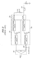
- the power amplifying apparatus shown in Fig. 5 includes an asymmetric power driver 500, a transmission line 502, a carrier amplifier 504 and a peaking amplifier 506 connected in parallel, an offset line 508, a first quarter-wave transmission line 510 and a second quarter-wave transmission line 512.
- the carrier amplifier 504 forms a Doherty amplifier together with the peaking amplifier 506.
- the carrier and the pecking amplifier 504 and 506 have the same input and output matching circuits, respectively.
- the asymmetric power driver 500 performs an asymmetric power drive to the carrier and the peaking amplifier 504 and 506. Preferably, more power is supplied to the peaking amplifier 506 than to the carrier amplifier 504.
- a power capacity is measured in "gm" and a unit thereof is I/V. Further, the power capacity also denotes a device size.
- asymmetric power driver 500 With the asymmetric power driver 500, asymmetric power is provided to the carrier and the peaking amplifiers 504 and 506 without providing the symmetric power to the carrier and the peaking amplifiers 504 and 506 as in a conventional case.
- the asymmetric power driver 500 will be described in detail with reference to Fig. 12.
- the transmission line 502 serves to synchronize phases between the carrier and the peaking amplifiers 504 and 506. More specifically, the transmission line 502 allows each of the amplifiers 504 and 506 to have the same input/output matching circuits so that each of the amplifiers can output at the same characteristic impedance, e.g., 50 Ohm, thereby enabling the production of a maximum output from the Doherty amplifier.
- the power amplifying apparatus can also be implemented in a manner that a maximum output is obtained from the Doherty amplifier by forming different input and output matching circuits in the carrier and the peaking amplifiers 504 and 506.
- the load impedances of the carrier and the peaking amplifiers must be reduced appropriately for better linearity and also for proper power matching.
- the load impedance of the peaking amplifier must be reduced more than that of the carrier amplifier, as shown in Fig. 10B, to thereby achieve a better linearity and a proper power matching.
- the offset line 508 permits to occur a proper load modulation by increasing impedance output while the peaking amplifier 506 is not operating.
- the first quarter-wave transmission line 510 serves as an impedance inverter, thereby implementing the Doherty operation.
- the first quarter-wave transmission line 510 reverses an output as 2R o , where R o denotes load impedance.
- the second quarter-wave transmission line 512 changes load impedance from 50 Ohm to 25 Ohm.
- the load impedance thereof should be made to have R o /N with respect to a characteristic impedance of 50 Ohm. For example, Fig.
- the second quarter-wave transmission line 512 for changing the load impedance from 50 Ohm to 25 Ohm, wherein the characteristic impedance of the second quarter-wave transmission line 512 can be expressed as ( 50 ⁇ 25 ) Ohm.
- the power amplifier shown in Fig. 5 is implemented by employing the asymmetric power driver 500, and has a configuration a parallel connection of the input/output matched carrier and peaking amplifiers 504 and 506.
- output ends of the two amplifiers 504 and 506 are implemented through a Doherty network composed of the offset line 508 and a quarter-wave transformer ( ⁇ /4 line) with the first and the second quarter-wave transmission lines 510 and 512.
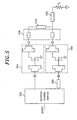
- Fig. 6 illustrates an N-way (where N is an integer equal to or greater than 2) power amplifying apparatus in accordance with another preferred embodiment of the present invention.
- the N-way Power amplifying apparatus includes an N-way asymmetric power driver 600, a transmission line block 602, a Doherty amplifier 604, an offset line 606 and a first and a second quarter-wave transmission line 608 and 610.
- the Doherty amplifier 604 is composed of N-number of amplifiers including a single carrier amplifier CA and the (N-1)-number of peaking amplifiers PA 1 to PA (N-1) , wherein each of the amplifiers has therein input and output matching circuits.
- the N-way asymmetric power driver 600 performs an asymmetric power drive on the carrier amplifier CA and the (N-1)-number of peaking amplifiers PA 1 to PA (N-1) , respectively.
- each power supplied to the (N-1)-number of peaking amplifiers is equal to or higher than that supplied to the carrier amplifier by more than a specific value.
- the N-way asymmetric power driver 600 can make the (N-1)-number of peaking amplifiers in an asymmetric power drive or a symmetric power drive. That is, either a same power or a separate power can be provided to each of the peaking amplifiers.
- N-way asymmetric power driver 600 it is also possible to allow the N-way asymmetric power driver 600 to respectively provide different input ratios to the input matching circuits in the peaking amplifiers.
- the carrier amplifier and the (N-1)-number peaking amplifiers can have different input and output matching circuits from each other, wherein the input and the output matching circuits in the (N-1)-number peaking amplifiers all have the same or different configurations.
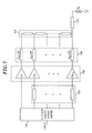
- Fig. 7 depicts an N-stage (where N is a positive integer equal to or greater than 2) power amplifying apparatus in accordance with further another preferred embodiment of the present invention.
- the N-stage Power amplifying apparatus includes an N-stage asymmetric power driver 700, a transmission line 702, a Doherty amplifier 704, an offset line 706, an N-number of first quarter-wave transmission lines 708 and a second quarter-wave transmission lines 708 and 710.
- the Doherty amplifier 704 is composed of N-number of amplifiers including a single carrier amplifier CA and (N-1)-number of peaking amplifiers PA 1 to PA (N-1) , wherein each of the carrier and the peaking amplifiers has therein input and output matching circuits.
- the embodiment described in Fig. 7 is substantially the same as that shown in Fig. 6 except that the first quarter-wave transmission lines 708 have a cascade connection.
- the Doherty amplifier gradually perform a Doherty operation in a manner similar to the power amplifier shown in Fig. 4. That is, the carrier amplifier CA is turned on and then a first peaking amplifier PA 1 is turned on, thereby performing the Doherty operation. Next, both the carrier amplifier CA and the first peaking amplifier PA 1 serve as a carrier amplifier together and, further, the second peaking amplifier PA 2 serves as a peaking amplifier, thereby performing the Doherty operation.
- maximum efficiency can be obtained from a much lower power level and, further, it is also possible to obtain the maximum efficiency at an intermediate level, so that high efficiency can be obtained over a full power range.
- the N-stage asymmetric power driver 700 performs a symmetric power drive on the carrier amplifier CA and the peaking amplifiers PA 1 to PA (N-1) . More specifically, the power supplied to the (N-1)-number of peaking amplifiers is higher than that supplied to the carrier amplifiers by more than a specific value.
- the N-stage asymmetric power driver 700 can provide asymmetric power having different input ratios to the input/output matching circuits in the peaking amplifiers.
- the carrier amplifier and the (N-1)-number of peaking amplifiers can have the same input/output matching circuits.
- the carrier amplifier and each of the peaking amplifiers can have different input/output matching circuits from each other, wherein the input/output matching circuits in the peaking amplifiers can be either same or different.
- the input/output matched carrier amplifier and peaking amplifiers have bias points biased as a class AB and a class C, respectively, and, therefore, they reveals the difference in the fundamental current components.
- the peaking amplifiers biased as the class C has less gain than the carrier amplifier. Accordingly, when the carrier amplifier reaches its maximum fundamental current level, the peaking amplifier does not reach its maximum fundamental current level.
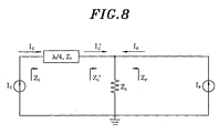
- Fig. 8 presents a conceptual diagram of the Power amplifying apparatus using an asymmetric power drive in accordance with the present invention.
- a carrier amplifier and a peaking amplifier are respectively indicated as current sources I C and I P , wherein load impedances of the carrier amplifier, the peaking amplifier and the Doherty amplifier are indicated as Z C , Z P and Z L , respectively.
- the peaking amplifier is turned off, which results in an open state of the current source I P .
- both the carrier and the peaking amplifiers operate and, thus, the load impedances of the amplifiers are determined by respective functions of the current sources, which are defined by the following Eq. 2.
- Fig. 9A expresses a graph for comparing fundamental current components according to an input voltage level between the conventional Doherty amplifier and the novel Power amplifying apparatus.
- the current components for the carrier amplifier and the peaking amplifier achieved through respective power driving can be expressed by a following Eq.
- the fundamental current component increases accordingly in the current source.
- the fundamental current component of the carrier amplifier reaches a maximum level, while the fundamental current components of the peaking amplifier does not reach the maximum level due to a bias difference to the carrier amplifier and the peaking amplifier. Therefore, as in the "even" mode (i.e., the symmetric power drive), there occurs a difference in the fundamental current component.
- Fig. 9B shows a graph illustrating a correlation between the load impedance and the input power level according to the fundamental current components of Fig. 9A.
- the load impedances are the same, i.e., 100 Ohm, in both the asymmetric power drive and the symmetric power drive.
- the power amplifying apparatus is widely used so that the maximum efficiency can be achieved at a point corresponding to a 1/4 of the maximum power thereof, which can be known by the load impedance.
- the load impedance starts to decrease.
- the load modulation does not properly occur and, accordingly, the carrier amplifier and the peaking amplifier have an impedance much greater than 50 Ohm at a point where a maximum output is produced.
- the carrier amplifier and the peaking amplifier have an impedance of 50 Ohm at a point where the maximum output is attained.
- the power amplifier using an asymmetric power drive in accordance with the present invention has high linearity while maintaining high efficiency and further produces a desired maximum output, thereby improving the overall utility of the solid-state device.
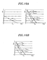
- Fig. 10A provides a graph showing changes of the load impedance of Fig. 9B in terms of a load line.
- a left graph in Fig. 10A illustrates a load line of the symmetric power drive and the asymmetric power drive, which is obtained when the peaking amplifier has just been turned on at a low power level.
- the load line is almost the same as that shown in Fig. 9B. That is, at the lower power level, the load impedance in the "asymmetric" and “symmetric” modes becomes twice, which is indicated by the load lines of the left graph of Fig. 10A.
- a right graph in Fig. 10A shows the load lines of the symmetric and the asymmetric power drives at a point where a maximum power is attained.
- Fig. 9B in case of the symmetric power drive, the maximum output cannot be achieved due to a large impedance. Moreover, in terms of linearity, a much lower load line is formed in comparison with the case of the symmetric power drive.
- the load line having the large impedance prevents a production of the maximum output, which means that, in the "asymmetric" Doherty amplifier in accordance with the present invention, it is possible to achieve the maximum output.
- Fig. 10B presents a graph illustrating load lines obtained by changing the load impedance of Fig. 9B in order to produce the maximum output of the power amplifying apparatus in accordance with the present invention.
- the matching circuits should be changed so that the load line in the asymmetric power drive can be obtained. As shown in Fig. 10B, if an inclination of the load line increases by decreasing the large impedance, an optimized load line can be achieved. Accordingly, it is possible to enhance the linearity of the Doherty amplifier using a symmetric power drive, and further, to attain the maximum power.
- Fig. 11A depicts a two-tone simulation graph between an inter-modulation three (IM3) level and an average output, wherein a reason that the Power amplifying apparatus using an asymmetric power drive in accordance with the present invention achieves the optimized linearity is analyzed by using the two-tone simulation.
- IM3 inter-modulation three
- IM3 denotes that an unknown signal is mixed with and then modulated together with two or more frequencies passing through a nonlinear system or a nonlinear circuit.
- IMD refers to a distortion generated by such an inter-modulation.
- the IM3 component i.e., two-tone frequencies f1 and f2
- multiple harmonics such as 2*f1, 3*f2 and so on can be removed by a filter.
- third order harmonic frequencies overlapped with the f1 and the f2 signal e.g., 2*f1-f2 and 2*f2-f1, cannot be removed even by the filter, they indicate an index of the linearity.
- the two-tone simulation indicates an analysis or a measurement performed by using two frequency components in a measuring device, a testing, a harmonic balance or the like.
- two-tone signals having offset frequencies are introduced about a central frequency, to thereby analyze the IMD between the two signals, i.e., the linearity of the amplifier.
- asymmetric power drive increases in term of the IM3
- x in l:x i.e., a ratio of the peaking power
- the distributions of IM3 levels in the carrier and the peaking amplifier become wider together in a region.
- the distributions of IM3 levels becomes narrower.
- the power amplifying apparatus having the optimized linearity proposed by the present invention achieves the high linearity by employing a method for offsetting the IM3 level of the carrier and the peaking amplifier.
- the IM3 level of each amplifier is lower than that of the class AB power amplifier.
- the carrier and the peaking amplifier should be so designed as to have the optimized linearity.
- the peaking amplifier is turned off and, further, only the carrier amplifier operates. Therefore, it is preferable to design the carrier amplifier so as to operate linearly.
- Matching variations (MV) illustrated in Figs. 11A and 11B were compared between the asymmetric power driven carrier and peaking amplifier that are so designed as to more linearly operate by employing the aforementioned concept.
- Fig. 11B represents a two-tone simulation graph between an IM3 phase and an average power, wherein a reason that the Power amplifying apparatus using the asymmetric power drive achieves the optimized linearity is analyzed by using the two-tone simulation as in Fig. 11A.
- the offset effect is produced.
- a region corresponding to the phase difference of 180 degrees is more widely distributed. That is, in the high power level, it is preferable to design the amplifiers in a way that the IM3 levels of the carrier and the peaking amplifier are the same and the phase difference therebetween becomes 180 degree, to thereby effectively carry out the offset of the amplifiers.
- the IM3 phase of the carrier amplifier increases from a low average output point toward a down (negative value) direction.
- the IM3 phase of the peaking amplifier increases toward an up (positive value) direction, thereby enlarging the region corresponding to the phase difference of 180 degree.
- the matching circuits are changed so as to achieve optimized impedance, the phases are not considerably changed, whereas the IM3 level decreases as shown in Fig. 11A.
- the IM3 level decreases in a high average output region. Accordingly, when the IM3 levels are low and same and the phases are opposite from each other, the carrier and the peaking amplifier can be linearly designed with a proper load modulation, thereby achieving the optimized linearity.
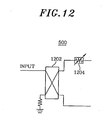
- Fig. 12 illustrates an example of the asymmetric power driver 500 illustrated in Fig. 5. Although it is not particularly described and shown, it is understood that the asymmetric power driver illustrated in Fig. 5 is equally applied to all the preferred embodiments of the power amplifying apparatus in accordance with the present invention.
- the asymmetric power driver 500 includes a 3dB hybrid coupler 1202 and an attenuator 1204.
- the 3dB hybrid coupler 1202 is used for a symmetric power drive and serves to couple an input power to the carrier amplifier 504 and the peaking amplifier 506.
- the attenuator 1204 is connected between the 3dB hybrid coupler 1202 and the carrier amplifier 504 to attenuate amplitude of the power to the carrier amplifier 504, thereby increasing a power to the peaking amplifier 506 relative to that of the carrier amplifier 504.
- the 3dB hybrid coupler may be substituted with a Wilkinson divider and, further, instead of the aforementioned attenuator 1204, an amplifier may be connected to an input matching circuit of the peaking amplifier 504, thereby enabling to increase the power drive of the peaking amplifier 504.
- the attenuator or the amplifier in this embodiment is connected to the input matching circuit of the carrier amplifier or that of the peaking amplifier, however, the connection of the attenuator or the amplifier may be changed for a relative difference in a power drive without being limited to the aforementioned connection.
- the asymmetric power drive in accordance with the present invention can employ a method for making input power supplied to the peaking amplifier higher than that supplied to the carrier amplifier by 4 dB through the use of a coupler having an optional coupling ratio, e.g., a 5 dB coupler such as 1A1305-5 available from Anaren, Inc. in U.S.A.
- a coupler having an optional coupling ratio e.g., a 5 dB coupler such as 1A1305-5 available from Anaren, Inc. in U.S.A.
- Figs. 13A and 13B describe examples of the carrier and the peaking amplifiers in accordance with the present invention.
- each of the carrier and the peaking amplifiers includes a metal oxide semiconductor (MOS) FET device, which has a gate terminal G for applying a gate bias together with an input matching circuit in the carrier/peaking amplifier, a drain terminal D for applying a drain bias together with an output matching circuit in the carrier/peaking amplifier and a source terminal S grounded to an earth.
- MOS metal oxide semiconductor
- each of the carrier and the peaking amplifiers includes a base junction transistor (BJT) device, which includes a base terminal B for applying a base bias together with the input matching circuit in the carrier/peaking amplifier, a collector terminal C for applying a collector bias together with the output matching circuit in the carrier/peaking amplifier and an emitter terminal E grounded to an earth.
- BJT base junction transistor
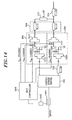
- Fig. 14 describes an exemplary block diagram of the power amplifying apparatus shown in Fig. 5 provided with a bias controller.
- the power amplifying apparatus includes a coupler 1400, a power detector 1402, a bias controller 1406, an asymmetric power divider 500, a transmission line 502, a carrier amplifier 504, a peaking amplifier 506, an offset line 508, a first quarter-wave transmission line 510 and a second quarter-wave transmission line 512.
- the carrier amplifier 504 is provided with a MOS FET 1410 described with reference to Fig. 13A, an input matching circuit 1412 and an output matching circuit 1414, wherein the input and the output matching circuits 1412 and 1414 are connected by the MOS FET 1410.
- the gate terminal G and the drain terminal D of the device 1410 are connected to the input and the output matching circuit 1412 and 1414, respectively.
- the peaking amplifier 506 is provided with MOS FET 1420, an input matching circuit 1422 and an output matching circuit 1424, wherein the input and the output matching circuits 1422 and 1424 are connected by the MOS FET 1420. More specifically, the gate terminal G and the drain terminal D of the device 1420 are connected to the input and the output matching circuit 1422 and 1424, respectively.
- the bias controller 1406 is connected to the carrier and the peaking amplifier 504 and 508, respectively.
- the bias controller 1406 controls a bias of the carrier and the peaking amplifiers 504 and 506, thereby optimizing the linearity and the efficiency of the power amplifying apparatus. More specifically, the bias controller 1406 applies gate bias voltages to the gate terminals G of the MOS FETs 1410 and 1420, respectively and further selectively applies drain bias voltages to the drain terminals D of the MOS FETs 1410 and 1420, respectively, thereby controlling the gate bias and the drain bias.
- this embodiment can employ the BJT device described in Fig. 13B as well as the MOS FET device of Fig. 13A.
- a connection relationship and an operation thereof can be easily understood by those who skilled in the art and, thus, a detailed explanation will be omitted.
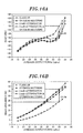
- Fig. 15A describes a graph showing an experiment result performed on the configuration shown in Fig. 12 so as to investigate an adjacent channel leakage ratio (ACLR), i.e., the linearity measured using an MRF281 device available from Motorola inc. in U.S.A., in terms of average output power.
- the ACLR denotes that a signal having a spectrum such as CDMA is compared using marker-to-marker on the spectrum between its own channel and an adjacent channel away from a frequency domain by a random offset.
- the ACLR indicates a value obtained by subtracting a marker of its own channel from another channel.
- the spectrum of the adjacent channel is generated by nonlinear characteristics of the amplifier.
- ACLR is used for an index representing the linearity of the amplifier.
- Fig. 15B illustrates a graph depicting a result of a drain efficiency experiment performed in terms of the average output power. As illustrated, the asymmetric power drive enables to achieve a high efficiency.
- the power amplifying apparatus using the asymmetric power drive can achieve high linearity while maintaining the high efficiency.
- Figs. 16A and 16B represent graphs showing an experiment result obtained by employing the asymmetric power drive, wherein improvement degrees of the matching variation (MV) efficiency and the linearity are also checked by optimizing the matching circuits during the symmetric power drive.
- MV matching variation
- Fig. 16A indicates ACLR characteristics in terms of the average output power.
- the ACLR is considerably improved in comparison with the class AB amplifier.
- the linearity is further improved in a high power level.
- Fig. 16B illustrates the drain efficiency in terms of the average output. In case the matching circuit and the asymmetric power drive have been employed, the higher efficiency is achieved.
- the present invention can solve problems raised in the conventional microwave Doherty amplifies in which an improper load modulation occurs and a maximum output is not produced, thereby achieving the high efficiency and the optimized linearity. If the present invention is employed in an existing mobile communication network or in CDMA base-stations/handsets, the high efficiency and linearity can be achieved, thereby improving price competitiveness and reliability. Especially, the present invention can be simply implemented at a low cost by using an asymmetric power driver or a coupler for an asymmetric power drive.
Abstract
Description
- The present invention relates to a high efficiency and linearity power amplifying apparatus; and, more particularly, to a power amplifying apparatus using an asymmetric power drive, which employs a microwave Doherty amplifier.
- As well-known in the art, a Doherty power amplifier has a structure of a carrier and a peaking amplifier connected in parallel by using a quarter-wave transformer (λ/4 line). Further, the Doherty amplifier is driven by a symmetrical power driving method in which the peaking amplifier controls a load impedance of the carrier amplifier by increasing the amount of current supplied to the load from the peaking amplifier as the power level is increased, thereby improving efficiency.
- A microwave Doherty amplifier has been used in an amplitude modulation (AM) transmitter of a broadcasting apparatus using a high-power low-frequency (LF) vacuum tube or a medium frequency (MF) vacuum tube. There have been a variety of proposals for implementing the microwave Doherty amplifier with a solid-state device without using a vacuum tube, and numerous researches have been conducted to implement the proposals.
- A Doherty amplifier employing an asymmetric power driving method has achieved high efficiency and linearity. Especially, the Doherty amplifier employed in base stations and handsets for mobile communications is implemented by using approximately same-sized solid-state devices, the same input and output matching circuits and an input power drive. In this case, a carrier amplifier is biased as a class AB, and a peaking amplifier a class C. Since the peaking amplifier has a lower bias than that of the carrier amplifier, it is problematic that the current level of the peaking amplifier is always lower than that of the carrier amplifier depending on a power level.
- Fig. 1 shows the amplitude of a current component according to each bias level, i.e., a conduction angle. As illustrated in Fig. 1, a fundamental current component's amplitude of the peaking amplifier biased at a lower level is lower than that of the carrier amplifier. The carrier amplifier whose bias point is the class AB has a conduction angle ranging from π to 2π and, therefore, has the amplitude of the fundamental current component ranging from 0.5 to 0.536 at a maximum input power. Meanwhile, the peaking amplifier operated in the class C has a conduction angle ranging from 0 to π and, thus, has the amplitude of the fundamental current component ranging from 0 to 0.5. Accordingly, the fundamental current component of the peaking amplifier does not reach that of the carrier amplifier. As a result, a load modulation (a phenomenon in which load impedance of the front end of a current source varies with an amplitude of current generated from the current source) occurs and, further, serious problems are caused in the Doherty operation.
- Moreover, as shown in Fig. 9A to be described later, due to the lower bias level of the peaking amplifier, the fundamental current component of the peaking amplifier is detected only when a driving voltage thereof is equal to or higher than a certain level.
- Therefore, if the carrier amplifier is driven at a maximum input power, the fundamental current component level of the peaking amplifier is lower than that of the carrier amplifier and, further, the peaking amplifier is not driven at the required maximum input power, thereby generating a much lower fundamental current. As a result, the Doherty amplifier is not able to generate a desired maximum output power.
- In order to overcome the above-described problems, a research finding has been published regarding considerably improved a typical Doherty amplifier in terms of a maximum output power while maintaining the high efficiency thereof by employing an envelope tracking device or an input power tracking device. Further, various researches have been done in order to actually implement the Doherty amplifier in a microwave bandwidth, and one of them is shown in Fig. 2.
- A Doherty amplifier shown in Fig. 2 includes a
carrier amplifier 204 and apeaking amplifier 206 in parallel; apower divider 200 for providing a same power to thecarrier amplifier 204 and thepeaking amplifier 206; atransmission line 202 for synchronizing phases between thecarrier amplifier 204 and the peakingamplifier 206; anoffset line 208 for generating a proper load modulation by increasing an impedance output while the peakingamplifier 206 is not operating; and quarter-wave transmission lines - Such Doherty amplifier as in Fig. 2 is implemented in a manner that the carrier amplifier and the peaking amplifier have the same input/output matching circuits and yields the same output, so that a maximum output can be produced by each Doherty amplifier. Further, by sequentially providing the output matching circuits and, in turn, the
offset line 208 at output ends of transistors in the carrier and the peaking amplifiers, an imaginary part as well as a real part can be matched, thereby enabling the Doherty operation while obtaining the maximum output power. (See, Y. Yang et al, "Optimum Design for Linearity and Efficiency of Microwave Doherty Amplifier Using a New Load Matching Technique," Microwave Journal,Vol 44, No. 12, pp. 20-36, Dec. 2002.) - Further, Fig. 3 provides an N-way Doherty amplifier having an optimum design for efficiency and linearity while improving a typical Doherty amplifier (See, Y. Yang et al, "A Fully Matched N-way Doherty Amplifier with Optimized Linearity," IEEE Trans. Microwave Theory and Tech., Vol. 51, No. 3, pp. 986-993, March 2003.)
- Unlike the configuration shown in Fig. 2, the N-way Doherty amplifier illustrated in Fig. 3 performs the Doherty operation with a
single carrier amplifier 302 and a (N-1)-number of peakingamplifiers 304. Further, an N-way splitter 300 is used for putting the same input into thesingle carrier amplifier 302 and the peakingamplifiers 304. - Fig. 4 presents an N-stage Doherty amplifier for gradually achieving high efficiency from a much lower power level in comparison with a general Doherty amplifier (See, N. Srirattana et al, "Analysis and design of a high efficiency multistage Doherty amplifier for WCDMA," EuMC Digest 2003, Vol. 3, pp. 1337-1340, Oct. 2003.) The Doherty amplifier shown in Fig. 4 has an N-
way power divider 400 for performing the Doherty operation by putting the same input into asingle carrier amplifier 402 and a (N-1)-number of peakingamplifiers 404. - The following is a brief explanation of the Doherty amplifier. First of all, the
carrier amplifier 402 is turned on and, then, a first peaking amplifier PA1 is turned on, to perform the Doherty operation. Thereafter, both of thecarrier amplifier 402 and the first peaking amplifier PA1 serve as a carrier amplifier while a second peaking amplifier PA2 serves as a peaking amplifier, thereby performing the Doherty operation together. Such operation is carried out up to a last peaking amplifier PAN-1. As the Doherty operation is performed gradually and successively as described above, maximum efficiency can be obtained from a much lower power level. Further, it is also possible to repeatedly obtain the maximum efficiency over intermediate power levels, so that high efficiency can be obtained over a full power level. - In the meantime, in order to solve a problem in which the Doherty amplifier do not produce a maximum power output due to a low bias when the Doherty amplifier is implemented by using a solid-state device, there has been proposed a Doherty amplifier by using an envelope tracking device (See, Y. Yang et al, "A Microwave Doherty Amplifier Employing Envelope Tracking Technique for High Efficiency and Linearity", IEEE Microwave and Wireless Components Letters, Vol. 13, No. 9, Sep. 2003., and J. Cha et al, "An Adaptive Bias Controlled Power Amplifier with a Load-Modulated Combining Scheme for High Efficiency and Linearity", IEEE MTT-S Int. Microwave Sympo. Vol. 1, pp. 81-84, June 2003.)
- However, even in the proposed Doherty amplifier, an additional device for controlling the power level of the peaking and the carrier power amplifiers is still required in order to achieve an improved linearity and the maximum output.
- It is, therefore, an object of the present invention to provide a Doherty amplifier using an asymmetric power drive, to thereby achieve optimized linearity while maintaining high efficiency.
- It is another object of the present invention to provide a power amplifying apparatus using the Doherty amplifier.
- In accordance with an aspect of the present invention, there is provided a power amplifying apparatus, which includes: a carrier amplifier and a peaking amplifier connected in parallel; and asymmetric power driving means for driving the carrier amplifier and the peaking amplifier using an asymmetric power drive.
- In accordance with another aspect of the present invention, there is provided a power amplifying apparatus, which includes: a Doherty amplifier having N-number of amplifiers connected in parallel, the N-number of amplifiers including a single carrier amplifier and (N-1)-number of peaking amplifiers; asymmetric power driving means for driving the N-number of amplifiers using an asymmetric power drive; and a Doherty network, connected to an output end of the Doherty amplifier, for controlling a load impedance of the amplifying apparatus to derive a load modulation of the Doherty amplifier.
- In accordance with further another aspect of the present invention, there is provided a Doherty power amplifier, which includes: a carrier amplifier and one or more peaking amplifiers connected in parallel, each having input and output matching circuits, wherein the input and outputs matching circuits in the carrier and the peaking amplifiers are made different from each other in a manner that load impedances of the carrier and the peaking amplifiers are reduced for proper power matching.
- The above and other objects and features of the present invention will become apparent from the following description of preferred embodiments, given in conjunction with the accompanying drawings, in which:
- Fig. 1 shows a graph for comparing a fundamental current component between a carrier amplifier and a peaking amplifier in a conventional Doherty amplifier;
- Fig. 2 describes a block diagram of a conventional Doherty amplifier;
- Fig. 3 provides a block diagram of conventional N-way Doherty power amplifying apparatus employing a symmetric power driver;
- Fig. 4 illustrates a block diagram of conventional N-stage Doherty power amplifying apparatus employing a symmetric power driver;
- Fig. 5 offers an exemplary block diagram of an N-way (N=2) power amplifying apparatus using an asymmetric power drive in accordance with a preferred embodiment of the present invention;
- Fig. 6 presents a block diagram of an N-way (where N is a positive integer equal to or greater than 2) power amplifying apparatus using an asymmetric power drive in accordance with another preferred embodiment of the present invention;
- Fig. 7 illustrates a block diagram of an N-stage (where N is a positive integer equal to or greater than 2) power amplifying apparatus using an asymmetric power drive in accordance with further another preferred embodiment of the present invention;
- Fig. 8 depicts a diagram for explaining an operation principal of a Doherty amplifier in accordance with the present invention;
- Fig. 9A describes a graph for comparing a fundamental current component to an input power level between the conventional Doherty power amplifying apparatus in Fig. 3 and the novel power amplifying apparatus in Fig. 6;
- Fig. 9B shows a graph illustrating an impedance distribution to an input power level for explaining a load modulation occurred in the power amplifying apparatus shown in Fig. 6;
- Fig. 10A provides a graph showing the load impedance of Fig. 9B in terms of a load line;
- Fig. 10B presents a graph illustrating a load line, which is achieved by varying matching circuits to derive the changes of the load impedance of Fig. 9B in order to obtain a maximum output from the power amplifying apparatus in accordance with the present invention;
- Fig. 11A depicts a two-tone simulation graph between an IM3 level and an average output;
- Fig. 11B represents a two-tone simulation graph between an IM3 phase and an average output;
- Fig. 12 offers a detailed block diagram of the asymmetric power driver shown in Figs. 5 and 6;
- Fig. 13A illustrates a metal oxide semiconductor (MOS) device employed in the power amplifying apparatus in accordance with the present invention;
- Fig. 13B depicts a base junction transistor (BJT) device employed in the power amplifying apparatus in accordance with the present invention; and
- Fig. 14 describes a block diagram of a power amplifying apparatus having a bias controller in accordance with the present invention;
- Fig. 15A describes a correlation graph between an adjacent channel leakage ratio (ACLR) and average output power of the power amplifying apparatus shown in accordance with the present invention;
- Fig. 15B illustrates a correlation graph between drain efficiency and average output power of the power amplifying apparatus in accordance with the present invention;
- Fig. 16A is a correlation graph between an ACLR and average output power in an optimized matching circuit; and
- Fig. 16B shows a correlation graph between drain efficiency and the average output power in an optimized matching circuit.
- Hereinafter, preferred embodiments of the present invention will be described in detail with reference to the accompanying drawings.
- Fig. 5 offers a block diagram of an N-way (in case of N=2) power amplifying apparatus using an asymmetric power drive in accordance with a preferred embodiment of the present invention. The power amplifying apparatus shown in Fig. 5 includes an
asymmetric power driver 500, atransmission line 502, acarrier amplifier 504 and a peakingamplifier 506 connected in parallel, an offsetline 508, a first quarter-wave transmission line 510 and a second quarter-wave transmission line 512. - The
carrier amplifier 504 forms a Doherty amplifier together with the peakingamplifier 506. The carrier and thepecking amplifier - The
asymmetric power driver 500 performs an asymmetric power drive to the carrier and the peakingamplifier amplifier 506 than to thecarrier amplifier 504. Herein, a power capacity is measured in "gm" and a unit thereof is I/V. Further, the power capacity also denotes a device size. - With the
asymmetric power driver 500, asymmetric power is provided to the carrier and the peakingamplifiers amplifiers asymmetric power driver 500 will be described in detail with reference to Fig. 12. - The
transmission line 502 serves to synchronize phases between the carrier and the peakingamplifiers transmission line 502 allows each of theamplifiers - Alternatively, the power amplifying apparatus according to the present invention can also be implemented in a manner that a maximum output is obtained from the Doherty amplifier by forming different input and output matching circuits in the carrier and the peaking
amplifiers - The offset
line 508 permits to occur a proper load modulation by increasing impedance output while the peakingamplifier 506 is not operating. - The first quarter-
wave transmission line 510 serves as an impedance inverter, thereby implementing the Doherty operation. For example, the first quarter-wave transmission line 510 reverses an output as 2Ro, where Ro denotes load impedance. The second quarter-wave transmission line 512 changes load impedance from 50 Ohm to 25 Ohm. In this case, since the Power amplifying apparatus is formed by connecting asingle carrier amplifier 504 and a (N-1)-number of peakingamplifiers 506 in parallel, the load impedance thereof should be made to have Ro/N with respect to a characteristic impedance of 50 Ohm. For example, Fig. 5 shows the 2-way power amplifying apparatus (i.e., N=2) and, therefore, there should be provided the second quarter-wave transmission line 512 for changing the load impedance from 50 Ohm to 25 Ohm, wherein the characteristic impedance of the second quarter-wave transmission line 512 can be expressed as
- As described above, the power amplifier shown in Fig. 5 is implemented by employing the
asymmetric power driver 500, and has a configuration a parallel connection of the input/output matched carrier and peakingamplifiers amplifiers line 508 and a quarter-wave transformer (λ/4 line) with the first and the second quarter-wave transmission lines - Fig. 6 illustrates an N-way (where N is an integer equal to or greater than 2) power amplifying apparatus in accordance with another preferred embodiment of the present invention. The N-way Power amplifying apparatus includes an N-way
asymmetric power driver 600, atransmission line block 602, aDoherty amplifier 604, an offsetline 606 and a first and a second quarter-wave transmission line - The
Doherty amplifier 604 is composed of N-number of amplifiers including a single carrier amplifier CA and the (N-1)-number of peaking amplifiers PA1 to PA(N-1), wherein each of the amplifiers has therein input and output matching circuits. - The N-way
asymmetric power driver 600 performs an asymmetric power drive on the carrier amplifier CA and the (N-1)-number of peaking amplifiers PA1 to PA(N-1), respectively. In accordance with the present invention, each power supplied to the (N-1)-number of peaking amplifiers is equal to or higher than that supplied to the carrier amplifier by more than a specific value. In this regard, the N-wayasymmetric power driver 600 can make the (N-1)-number of peaking amplifiers in an asymmetric power drive or a symmetric power drive. That is, either a same power or a separate power can be provided to each of the peaking amplifiers. - Alternatively, it is also possible to allow the N-way
asymmetric power driver 600 to respectively provide different input ratios to the input matching circuits in the peaking amplifiers. - Moreover, in order to perform the asymmetric power drive, it is possible to make the input/output matching circuits same in the carrier amplifier and the (N-1)-number peaking amplifiers. Alternatively, the carrier amplifier and the (N-1)-number peaking amplifiers can have different input and output matching circuits from each other, wherein the input and the output matching circuits in the (N-1)-number peaking amplifiers all have the same or different configurations.
- Fig. 7 depicts an N-stage (where N is a positive integer equal to or greater than 2) power amplifying apparatus in accordance with further another preferred embodiment of the present invention. The N-stage Power amplifying apparatus includes an N-stage
asymmetric power driver 700, atransmission line 702, aDoherty amplifier 704, an offsetline 706, an N-number of first quarter-wave transmission lines 708 and a second quarter-wave transmission lines Doherty amplifier 704 is composed of N-number of amplifiers including a single carrier amplifier CA and (N-1)-number of peaking amplifiers PA1 to PA(N-1), wherein each of the carrier and the peaking amplifiers has therein input and output matching circuits. - The embodiment described in Fig. 7 is substantially the same as that shown in Fig. 6 except that the first quarter-
wave transmission lines 708 have a cascade connection. The Doherty amplifier gradually perform a Doherty operation in a manner similar to the power amplifier shown in Fig. 4. That is, the carrier amplifier CA is turned on and then a first peaking amplifier PA1 is turned on, thereby performing the Doherty operation. Next, both the carrier amplifier CA and the first peaking amplifier PA1 serve as a carrier amplifier together and, further, the second peaking amplifier PA2 serves as a peaking amplifier, thereby performing the Doherty operation. With such configuration, maximum efficiency can be obtained from a much lower power level and, further, it is also possible to obtain the maximum efficiency at an intermediate level, so that high efficiency can be obtained over a full power range. - The N-stage
asymmetric power driver 700 performs a symmetric power drive on the carrier amplifier CA and the peaking amplifiers PA1 to PA(N-1). More specifically, the power supplied to the (N-1)-number of peaking amplifiers is higher than that supplied to the carrier amplifiers by more than a specific value. - Alternatively, it is also possible to allow the N-stage
asymmetric power driver 700 to provide asymmetric power having different input ratios to the input/output matching circuits in the peaking amplifiers. Furthermore, the carrier amplifier and the (N-1)-number of peaking amplifiers can have the same input/output matching circuits. Or, the carrier amplifier and each of the peaking amplifiers can have different input/output matching circuits from each other, wherein the input/output matching circuits in the peaking amplifiers can be either same or different. - Meanwhile, as described in Fig. 1, the input/output matched carrier amplifier and peaking amplifiers have bias points biased as a class AB and a class C, respectively, and, therefore, they reveals the difference in the fundamental current components. At this time, the peaking amplifiers biased as the class C has less gain than the carrier amplifier. Accordingly, when the carrier amplifier reaches its maximum fundamental current level, the peaking amplifier does not reach its maximum fundamental current level. Such ratio is expressed by σ defined as:

where I1,C and I1,P indicate the fundamental current components of the carrier amplifier and the peaking amplifiers, respectively; K denotes the portion of the voltage where the peaking amplifier starts to conduct; and I 1,P ·(1-K) describes the fundamental current level of the peaking amplifier at the maximum input drive for the carrier amplifier. - Fig. 8 presents a conceptual diagram of the Power amplifying apparatus using an asymmetric power drive in accordance with the present invention.
- As illustrated in Fig. 8, a carrier amplifier and a peaking amplifier are respectively indicated as current sources IC and IP, wherein load impedances of the carrier amplifier, the peaking amplifier and the Doherty amplifier are indicated as ZC, ZP and ZL, respectively.
- First of all, in a low power region (0 < Vin < K·Vin,max), the peaking amplifier is turned off, which results in an open state of the current source IP. Thus, the carrier amplifier operates depending on a quarter-wave transmission line (= λ/4 line) and the load impedance of the Doherty amplifier ZL.
- Further, in a high power region (K·Vin,max < Vin < Vin, max), both the carrier and the peaking amplifiers operate and, thus, the load impedances of the amplifiers are determined by respective functions of the current sources, which are defined by the following Eq. 2.


- Fig. 9A expresses a graph for comparing fundamental current components according to an input voltage level between the conventional Doherty amplifier and the novel Power amplifying apparatus. The current components for the carrier amplifier and the peaking amplifier achieved through respective power driving can be expressed by a following Eq. 3 (herein, a symmetric power driven amplifier is indicated as "even", whereas an asymmetric power driven amplifier is indicated as "uneven"):


where K·V in,max indicates an input voltage level at which peaking amplifier of the class C is triggered at low bias. - As depicted in Fig. 9A, as the input power increases, the fundamental current component increases accordingly in the current source. At this time, if the input power is equally applied to the carrier amplifier and the peaking amplifier, the fundamental current component of the carrier amplifier reaches a maximum level, while the fundamental current components of the peaking amplifier does not reach the maximum level due to a bias difference to the carrier amplifier and the peaking amplifier. Therefore, as in the "even" mode (i.e., the symmetric power drive), there occurs a difference in the fundamental current component.
- To overcome such issues, the present invention employs an "uneven" mode (i.e., the asymmetric power drive), to thereby equalize the fundamental current components of the carrier amplifier and the peaking amplifier depending on the maximum input power. Fig. 9B shows a graph illustrating a correlation between the load impedance and the input power level according to the fundamental current components of Fig. 9A.
- As shown in Fig. 9B, in a low power level where only the carrier amplifier operates, the load impedances are the same, i.e., 100 Ohm, in both the asymmetric power drive and the symmetric power drive. In other words, in the low power level, only the carrier amplifier operates at the load impedance of 100 Ohm that is twice 50 Ohm. Therefore, the power amplifying apparatus is widely used so that the maximum efficiency can be achieved at a point corresponding to a 1/4 of the maximum power thereof, which can be known by the load impedance. However, in a high power level, when the peaking amplifier just starts to conduct, the load impedance starts to decrease.
- In the conventional amplifier using a symmetric power drive, the load modulation does not properly occur and, accordingly, the carrier amplifier and the peaking amplifier have an impedance much greater than 50 Ohm at a point where a maximum output is produced. In other words, as illustrated in Fig. 9B, in the high power range, only when the load impedance changes from infinite peaking impedance to 50 Ohm, the maximum output of the Doherty amplifier can be obtained. However, in the "symmetric" mode, such operation is not carried out. On the other hand, in the amplifier using an asymmetric power drive in accordance with the present invention, the carrier amplifier and the peaking amplifier have an impedance of 50 Ohm at a point where the maximum output is attained. And, also, in the entire high power region, the load modulation occurs at a lower impedance in comparison with the case of an amplifier using a symmetric power drive. Therefore, the power amplifier using an asymmetric power drive in accordance with the present invention has high linearity while maintaining high efficiency and further produces a desired maximum output, thereby improving the overall utility of the solid-state device.
- Fig. 10A provides a graph showing changes of the load impedance of Fig. 9B in terms of a load line.
- A left graph in Fig. 10A illustrates a load line of the symmetric power drive and the asymmetric power drive, which is obtained when the peaking amplifier has just been turned on at a low power level. The load line is almost the same as that shown in Fig. 9B. That is, at the lower power level, the load impedance in the "asymmetric" and "symmetric" modes becomes twice, which is indicated by the load lines of the left graph of Fig. 10A.
- A right graph in Fig. 10A shows the load lines of the symmetric and the asymmetric power drives at a point where a maximum power is attained. As shown in Fig. 9B, in case of the symmetric power drive, the maximum output cannot be achieved due to a large impedance. Moreover, in terms of linearity, a much lower load line is formed in comparison with the case of the symmetric power drive. In other words, in the "symmetric" Doherty amplifier, i.e., in the conventional Doherty amplifier having comparatively large impedance due to an improper load modulation, the load line having the large impedance prevents a production of the maximum output, which means that, in the "asymmetric" Doherty amplifier in accordance with the present invention, it is possible to achieve the maximum output.
- Fig. 10B presents a graph illustrating load lines obtained by changing the load impedance of Fig. 9B in order to produce the maximum output of the power amplifying apparatus in accordance with the present invention.
- In order to produce the maximum power for the large impedance caused by the improper load modulation in the Doherty amplifier using a symmetric power drive and further to enhance the linearity, the matching circuits should be changed so that the load line in the asymmetric power drive can be obtained. As shown in Fig. 10B, if an inclination of the load line increases by decreasing the large impedance, an optimized load line can be achieved. Accordingly, it is possible to enhance the linearity of the Doherty amplifier using a symmetric power drive, and further, to attain the maximum power.
- Fig. 11A depicts a two-tone simulation graph between an inter-modulation three (IM3) level and an average output, wherein a reason that the Power amplifying apparatus using an asymmetric power drive in accordance with the present invention achieves the optimized linearity is analyzed by using the two-tone simulation.
- For reference, IM3 denotes that an unknown signal is mixed with and then modulated together with two or more frequencies passing through a nonlinear system or a nonlinear circuit. Further, IMD refers to a distortion generated by such an inter-modulation. Especially, in case of the IM3 component, i.e., two-tone frequencies f1 and f2, although a signal having various hybrid components is outputted, multiple harmonics such as 2*f1, 3*f2 and so on can be removed by a filter. Since, however, third order harmonic frequencies overlapped with the f1 and the f2 signal, e.g., 2*f1-f2 and 2*f2-f1, cannot be removed even by the filter, they indicate an index of the linearity.
- Moreover, the two-tone simulation indicates an analysis or a measurement performed by using two frequency components in a measuring device, a testing, a harmonic balance or the like. In case of measuring IMD and IM3, two-tone signals having offset frequencies (two-tone spacing) are introduced about a central frequency, to thereby analyze the IMD between the two signals, i.e., the linearity of the amplifier.
- As shown in Fig. 11A, if the asymmetric power drive increases in term of the IM3, in other words, if x in l:x, i.e., a ratio of the peaking power, increases, the distributions of IM3 levels in the carrier and the peaking amplifier become wider together in a region. On the other hand, in case where phases become opposite gradually by a decrease of the output power, the distributions of IM3 levels becomes narrower.
- That is, the power amplifying apparatus having the optimized linearity proposed by the present invention achieves the high linearity by employing a method for offsetting the IM3 level of the carrier and the peaking amplifier. In this case, the IM3 level of each amplifier is lower than that of the class AB power amplifier. Moreover, as the level becomes lower, the IM3 level is further offset, thereby considerably improving the linearity. Accordingly, the carrier and the peaking amplifier should be so designed as to have the optimized linearity. Especially, in a low power level, the peaking amplifier is turned off and, further, only the carrier amplifier operates. Therefore, it is preferable to design the carrier amplifier so as to operate linearly. Matching variations (MV) illustrated in Figs. 11A and 11B were compared between the asymmetric power driven carrier and peaking amplifier that are so designed as to more linearly operate by employing the aforementioned concept.
- Fig. 11B represents a two-tone simulation graph between an IM3 phase and an average power, wherein a reason that the Power amplifying apparatus using the asymmetric power drive achieves the optimized linearity is analyzed by using the two-tone simulation as in Fig. 11A.
- As illustrated, when the phase difference between the carrier amplifier and the peaking amplifier becomes 180 degrees due to the increase of the output power and the IM3 levels of the amplifiers are the same, the offset effect is produced. In case of the power amplifiers using the asymmetric power drive, a region corresponding to the phase difference of 180 degrees is more widely distributed. That is, in the high power level, it is preferable to design the amplifiers in a way that the IM3 levels of the carrier and the peaking amplifier are the same and the phase difference therebetween becomes 180 degree, to thereby effectively carry out the offset of the amplifiers. To summarize, referring to Fig. 11B, as the asymmetric power drive increases, the IM3 phase of the carrier amplifier increases from a low average output point toward a down (negative value) direction. In contrast, the IM3 phase of the peaking amplifier increases toward an up (positive value) direction, thereby enlarging the region corresponding to the phase difference of 180 degree. Further, if the matching circuits are changed so as to achieve optimized impedance, the phases are not considerably changed, whereas the IM3 level decreases as shown in Fig. 11A. Furthermore, as the asymmetric power drive increases, the IM3 level decreases in a high average output region. Accordingly, when the IM3 levels are low and same and the phases are opposite from each other, the carrier and the peaking amplifier can be linearly designed with a proper load modulation, thereby achieving the optimized linearity.
- Fig. 12 illustrates an example of the
asymmetric power driver 500 illustrated in Fig. 5. Although it is not particularly described and shown, it is understood that the asymmetric power driver illustrated in Fig. 5 is equally applied to all the preferred embodiments of the power amplifying apparatus in accordance with the present invention. - The
asymmetric power driver 500 includes a3dB hybrid coupler 1202 and anattenuator 1204. The3dB hybrid coupler 1202 is used for a symmetric power drive and serves to couple an input power to thecarrier amplifier 504 and the peakingamplifier 506. Theattenuator 1204 is connected between the3dB hybrid coupler 1202 and thecarrier amplifier 504 to attenuate amplitude of the power to thecarrier amplifier 504, thereby increasing a power to the peakingamplifier 506 relative to that of thecarrier amplifier 504. - Alternatively, the 3dB hybrid coupler may be substituted with a Wilkinson divider and, further, instead of the
aforementioned attenuator 1204, an amplifier may be connected to an input matching circuit of the peakingamplifier 504, thereby enabling to increase the power drive of the peakingamplifier 504. - It has been described that the attenuator or the amplifier in this embodiment is connected to the input matching circuit of the carrier amplifier or that of the peaking amplifier, however, the connection of the attenuator or the amplifier may be changed for a relative difference in a power drive without being limited to the aforementioned connection.
- Furthermore, the asymmetric power drive in accordance with the present invention can employ a method for making input power supplied to the peaking amplifier higher than that supplied to the carrier amplifier by 4 dB through the use of a coupler having an optional coupling ratio, e.g., a 5 dB coupler such as 1A1305-5 available from Anaren, Inc. in U.S.A.
- Figs. 13A and 13B describe examples of the carrier and the peaking amplifiers in accordance with the present invention.
- As shown in Fig. 13A, each of the carrier and the peaking amplifiers includes a metal oxide semiconductor (MOS) FET device, which has a gate terminal G for applying a gate bias together with an input matching circuit in the carrier/peaking amplifier, a drain terminal D for applying a drain bias together with an output matching circuit in the carrier/peaking amplifier and a source terminal S grounded to an earth.
- As shown in Fig. 13B, each of the carrier and the peaking amplifiers includes a base junction transistor (BJT) device, which includes a base terminal B for applying a base bias together with the input matching circuit in the carrier/peaking amplifier, a collector terminal C for applying a collector bias together with the output matching circuit in the carrier/peaking amplifier and an emitter terminal E grounded to an earth.
- Fig. 14 describes an exemplary block diagram of the power amplifying apparatus shown in Fig. 5 provided with a bias controller.
- The power amplifying apparatus includes a
coupler 1400, apower detector 1402, abias controller 1406, anasymmetric power divider 500, atransmission line 502, acarrier amplifier 504, a peakingamplifier 506, an offsetline 508, a first quarter-wave transmission line 510 and a second quarter-wave transmission line 512. - The
carrier amplifier 504 is provided with a MOS FET 1410 described with reference to Fig. 13A, aninput matching circuit 1412 and anoutput matching circuit 1414, wherein the input and theoutput matching circuits output matching circuit - Similarly, the peaking
amplifier 506 is provided withMOS FET 1420, aninput matching circuit 1422 and anoutput matching circuit 1424, wherein the input and theoutput matching circuits MOS FET 1420. More specifically, the gate terminal G and the drain terminal D of thedevice 1420 are connected to the input and theoutput matching circuit - The
bias controller 1406 is connected to the carrier and the peakingamplifier bias controller 1406 controls a bias of the carrier and the peakingamplifiers bias controller 1406 applies gate bias voltages to the gate terminals G of theMOS FETs 1410 and 1420, respectively and further selectively applies drain bias voltages to the drain terminals D of theMOS FETs 1410 and 1420, respectively, thereby controlling the gate bias and the drain bias. - Remaining components are the same as those described in Fig. 5 and, thus, a detailed description thereof will be omitted for simplicity.
- In this case, this embodiment can employ the BJT device described in Fig. 13B as well as the MOS FET device of Fig. 13A. A connection relationship and an operation thereof can be easily understood by those who skilled in the art and, thus, a detailed explanation will be omitted.
- Hereinafter, the efficiency and linearity of the power amplifying apparatus having the aforementioned asymmetric power driver will be considered with reference to Figs. 15A and 15B.
- Fig. 15A describes a graph showing an experiment result performed on the configuration shown in Fig. 12 so as to investigate an adjacent channel leakage ratio (ACLR), i.e., the linearity measured using an MRF281 device available from Motorola inc. in U.S.A., in terms of average output power. The ACLR denotes that a signal having a spectrum such as CDMA is compared using marker-to-marker on the spectrum between its own channel and an adjacent channel away from a frequency domain by a random offset. In other words, the ACLR indicates a value obtained by subtracting a marker of its own channel from another channel. The spectrum of the adjacent channel is generated by nonlinear characteristics of the amplifier. And also, ACLR is used for an index representing the linearity of the amplifier.
- As shown in Fig. 15A, as the uneven ratio increases, the linearity becomes improved. This proves that the maximum output increases and, further, the performance is improved in terms of the efficiency.
- Fig. 15B illustrates a graph depicting a result of a drain efficiency experiment performed in terms of the average output power. As illustrated, the asymmetric power drive enables to achieve a high efficiency.
- Based on such result, the power amplifying apparatus using the asymmetric power drive can achieve high linearity while maintaining the high efficiency.
- Figs. 16A and 16B represent graphs showing an experiment result obtained by employing the asymmetric power drive, wherein improvement degrees of the matching variation (MV) efficiency and the linearity are also checked by optimizing the matching circuits during the symmetric power drive.
- Above all, Fig. 16A indicates ACLR characteristics in terms of the average output power. When the symmetric power drive has been employed and the matching circuit has been optimized, the ACLR is considerably improved in comparison with the class AB amplifier. Further, in case the matching circuit and the asymmetric power drive have been employed, the linearity is further improved in a high power level.
- Fig. 16B illustrates the drain efficiency in terms of the average output. In case the matching circuit and the asymmetric power drive have been employed, the higher efficiency is achieved.
- As a result, in case the conventional symmetric power drive has been employed; the loads of the carrier and the peaking amplifier considerably increase, thereby preventing the implementation of the optimized performance. Meanwhile, in case the asymmetric power drive in accordance with the present invention has been employed, it is possible to achieve the optimized linearity and the high efficiency.
- The present invention can solve problems raised in the conventional microwave Doherty amplifies in which an improper load modulation occurs and a maximum output is not produced, thereby achieving the high efficiency and the optimized linearity. If the present invention is employed in an existing mobile communication network or in CDMA base-stations/handsets, the high efficiency and linearity can be achieved, thereby improving price competitiveness and reliability. Especially, the present invention can be simply implemented at a low cost by using an asymmetric power driver or a coupler for an asymmetric power drive.
- While the invention has been shown and described with respect to the preferred embodiments, it will be understood by those skilled in the art that various changes and modification may be made without departing from the scope of the invention as defined in the following claims.
Claims (21)
- A Doherty amplifier, comprising:a carrier amplifier and a peaking amplifier connected in parallel; andasymmetric power driving means for driving the carrier amplifier and the peaking amplifier using an asymmetric power drive.
- The Doherty amplifier of claim 1, wherein the asymmetric power driving means supplies a power to the peaking amplifier higher than that supplied to the carrier amplifier.
- The Doherty amplifier of claim 1, wherein the asymmetric power driving means supplies an identical power to the carrier amplifier and the peaking amplifier and wherein a device size of the carrier amplifier is different from that of the peaking amplifier.
- The Doherty amplifier of claim 1, wherein the asymmetric power driving means includes a coupler having an optional coupling ratio.
- The Doherty amplifier of claim 1, wherein the asymmetric power driving means includes:a power divider for distributing an input power to the carrier amplifier and the peaking amplifier; andan attenuator, interposed between the power divider and the carrier amplifier, for attenuating an amplitude of a power to the carrier amplifier.
- The Doherty amplifier of claim 1, wherein the asymmetric power driving means includes:a power divider for distributing an input power to the carrier amplifier and the peaking amplifier; andan amplifier, interposed between the power divider and the peaking amplifier, for amplifying an amplitude of a power distributed to the peaking amplifier.
- A power amplifying apparatus, comprising:a Doherty amplifier having N-number of amplifiers connected in parallel, the N-number of amplifiers including a single carrier amplifier and (N-1)-number of peaking amplifiers;asymmetric power driving means for driving the N-number of amplifiers using an asymmetric power drive; anda Doherty network, connected to an output end of the Doherty amplifier, for controlling a load impedance of the amplifying apparatus.
- The power amplifying apparatus of claim 7, wherein the asymmetric power driving means supplies powers to the (N-1)-number of peaking amplifiers higher than that supplied to the carrier amplifier.
- The power amplifying apparatus of claim 8, wherein amplitudes of the powers to the (N-1)-number of peaking amplifiers are identical to each other.
- The power amplifying apparatus of claim 8, wherein amplitudes of the powers to the (N-1)-number of peaking amplifiers are different from each other.
- The power amplifying apparatus of claim 7, wherein the asymmetric power driving means supplies identical powers to the carrier amplifier and the peaking amplifiers and wherein a device size of the carrier amplifier is different from those of the peaking amplifiers.
- The power amplifying apparatus of claim 7, wherein the asymmetric power driving means includes:a power divider for dividing an input power into N-way; andan attenuator, interposed between the power divider and the carrier amplifier, for attenuating an amplitude of a power to the carrier amplifier.
- The power amplifying apparatus of claim 7, wherein the asymmetric power driving means includes:an optional coupler for distributing an input power to the carrier amplifier and the peaking amplifiers; andan amplifier, interposed between the optional coupler and the peaking amplifiers, for amplifying an amplitude of powers distributed to the peaking amplifiers.
- The power amplifying apparatus of claim 7, wherein the Doherty network includes:an N-number of offset lines connected to the carrier amplifier and the (N-1)-number of peaking amplifiers, respectively, for controlling a load impedance while the (N-1)-number of peaking amplifiers are not operating;a first quarter-wave transmission line, connected to an output end of the offset line connected to the carrier amplifier, for changing the output impedance of the carrier amplifier into a 1/4 wavelength length; anda second quarter-wave transmission line, connected to output ends of the offset lines connected to the (N-1)-number of peaking amplifiers, changing the impedance through the offset lines into a 1/4 wavelength length in order to determine a load impedance of the Doherty amplifier.
- The power amplifying apparatus of claim 7, wherein the Doherty network includes:an N-number of offset lines connected to the carrier amplifier and the peaking amplifiers, respectively, for controlling the load impedance while the peaking amplifiers are not operating;an N-number of first quarter-wave transmission lines in a cascade type, each being connected to an output end of its corresponding offset line, for changing an output impedance of the carrier amplifier provided through the offset lines into a 1/4 wavelength length; anda second quarter-wave transmission line, connected to an output end of the first quarter-wave transmission lines, changing the output impedance provided through a proceeding offset line into a 1/4 wavelength length in order to determine a load impedance of the power amplifying apparatus.
- The power amplifying apparatus of claim 7, wherein each of the carrier amplifier and the peaking amplifiers includes:an input matching circuit;an output matching circuit; anda MOS FET (Metal Oxide Semiconductor Field Effect Transistor) connected between the input and the output matching circuits.
- The power amplifying apparatus of claim 7, wherein each of the carrier amplifier and the peaking amplifiers includes:an input matching circuit;an output matching circuit; anda BJT (Binary Junction Transistor) interposed between the input and the output matching circuits.
- The power amplifying apparatus of claim 16, wherein the power amplifying apparatus further comprises a bias controller for applying a gate bias and a drain bias to the MOS FET.
- The power amplifying apparatus of claim 17, wherein the power amplifying apparatus further comprises a bias controller for applying a base bias and a collector bias to the BJT.
- A power amplifying apparatus, comprising:a carrier amplifier and one or more peaking amplifiers connected in parallel, each having input and output matching circuits, wherein the input and outputs matching circuits in the carrier and the peaking amplifiers are made different from each other in a manner that load impedances of the carrier and the peaking amplifiers are reduced for proper power matching; andmeans for driving the carrier amplifier and the peaking amplifiers using either an asymmetric power drive or a symmetric power drive.
- The power amplifying apparatus of claim 20, wherein the load impedances of the carrier and the peaking amplifiers are lower than input impedances of the carrier and the peaking amplifiers.
Priority Applications (2)
| Application Number | Priority Date | Filing Date | Title |
|---|---|---|---|
| EP21169783.4A EP3893390A1 (en) | 2004-12-31 | 2005-12-23 | Power amplifying apparatus using asymmetric power drive |
| EP07015786.2A EP1848106B1 (en) | 2004-12-31 | 2005-12-23 | Power amplifying apparatus using asymmetric power drive |
Applications Claiming Priority (1)
| Application Number | Priority Date | Filing Date | Title |
|---|---|---|---|
| KR1020040117788A KR20060077818A (en) | 2004-12-31 | 2004-12-31 | High performance power amplifier using uneven power drive |
Related Child Applications (2)
| Application Number | Title | Priority Date | Filing Date |
|---|---|---|---|
| EP07015786.2A Division EP1848106B1 (en) | 2004-12-31 | 2005-12-23 | Power amplifying apparatus using asymmetric power drive |
| EP21169783.4A Division EP3893390A1 (en) | 2004-12-31 | 2005-12-23 | Power amplifying apparatus using asymmetric power drive |
Publications (1)
| Publication Number | Publication Date |
|---|---|
| EP1677414A1 true EP1677414A1 (en) | 2006-07-05 |
Family
ID=35589902
Family Applications (3)
| Application Number | Title | Priority Date | Filing Date |
|---|---|---|---|
| EP07015786.2A Active EP1848106B1 (en) | 2004-12-31 | 2005-12-23 | Power amplifying apparatus using asymmetric power drive |
| EP05028410A Withdrawn EP1677414A1 (en) | 2004-12-31 | 2005-12-23 | Power amplifying apparatus using asymmetric power drive |
| EP21169783.4A Pending EP3893390A1 (en) | 2004-12-31 | 2005-12-23 | Power amplifying apparatus using asymmetric power drive |
Family Applications Before (1)
| Application Number | Title | Priority Date | Filing Date |
|---|---|---|---|
| EP07015786.2A Active EP1848106B1 (en) | 2004-12-31 | 2005-12-23 | Power amplifying apparatus using asymmetric power drive |
Family Applications After (1)
| Application Number | Title | Priority Date | Filing Date |
|---|---|---|---|
| EP21169783.4A Pending EP3893390A1 (en) | 2004-12-31 | 2005-12-23 | Power amplifying apparatus using asymmetric power drive |
Country Status (6)
| Country | Link |
|---|---|
| US (1) | US7342444B2 (en) |
| EP (3) | EP1848106B1 (en) |
| JP (1) | JP4773199B2 (en) |
| KR (1) | KR20060077818A (en) |
| CN (1) | CN1822492B (en) |
| DE (1) | DE202005022009U1 (en) |
Cited By (17)
| Publication number | Priority date | Publication date | Assignee | Title |
|---|---|---|---|---|
| WO2008013481A1 (en) * | 2006-07-24 | 2008-01-31 | Telefonaktiebolaget Lm Ericsson (Publ). | A method for controlling a linear amplifier and power amplifier arrangement |
| WO2008062371A2 (en) * | 2006-11-23 | 2008-05-29 | Nxp B.V. | Integrated doherty type amplifier arrangement with high power efficiency |
| WO2009031097A1 (en) * | 2007-09-03 | 2009-03-12 | Nxp B.V. | Multi-way doherty amplifier |
| EP2145385A2 (en) * | 2007-04-23 | 2010-01-20 | Dali Systems Co. Ltd | N-way doherty distributed power amplifier |
| ITRM20080480A1 (en) * | 2008-09-04 | 2010-03-05 | Univ Roma | DOHERTY TYPE AMPLIFIER |
| EP2267885A1 (en) * | 2009-06-17 | 2010-12-29 | Nxp B.V. | Doherty amplifier |
| EP2403135A1 (en) * | 2010-06-24 | 2012-01-04 | Alcatel Lucent | Power amplifier for mobile telecommunications |
| EP2451074A1 (en) * | 2010-11-05 | 2012-05-09 | Postech Academy-Industry Foundation | Amplifier |
| EP2493069A1 (en) * | 2011-02-24 | 2012-08-29 | Postech Academy-Industry Foundation | Amplifier |
| WO2012143511A3 (en) * | 2011-04-21 | 2013-01-31 | Rwth Aachen | Linear amplifier arrangement for high-frequency signals |
| US8390381B2 (en) | 2010-06-02 | 2013-03-05 | Nxp B.V. | Two stage Doherty amplifier |
| EP2608400A1 (en) * | 2011-12-20 | 2013-06-26 | Nxp B.V. | N way Doherty amplifier |
| WO2015057118A1 (en) * | 2013-10-18 | 2015-04-23 | Telefonaktiebolaget L M Ericsson (Publ) | Power amplifier for amplification of an input signal into an output signal |
| EP2905896A1 (en) * | 2009-09-28 | 2015-08-12 | NEC Corporation | Doherty amplifier |
| US9184703B2 (en) | 2007-04-23 | 2015-11-10 | Dali Systems Co. Ltd. | N-way doherty distributed power amplifier with power tracking |
| EP3068046A1 (en) * | 2015-03-10 | 2016-09-14 | Fujitsu Limited | Wireless communication device and control method thereof |
| CN108123690A (en) * | 2016-11-30 | 2018-06-05 | 住友电工光电子器件创新株式会社 | Doherty amplifier |
Families Citing this family (59)
| Publication number | Priority date | Publication date | Assignee | Title |
|---|---|---|---|---|
| KR100553252B1 (en) * | 2002-02-01 | 2006-02-20 | 아바고테크놀로지스코리아 주식회사 | Power Amplification Apparatus of Portable Terminal |
| US7710202B2 (en) * | 2003-09-17 | 2010-05-04 | Nec Corporation | Amplifier |
| JP4858952B2 (en) * | 2005-05-23 | 2012-01-18 | 株式会社日立国際電気 | Amplifier |
| KR100749870B1 (en) * | 2006-06-07 | 2007-08-17 | (주) 와이팜 | Doherty amplifier |
| KR100814415B1 (en) * | 2007-02-14 | 2008-03-18 | 포항공과대학교 산학협력단 | Highly efficient doherty amplifier using a harmonic control circuit |
| JPWO2008136124A1 (en) * | 2007-04-26 | 2010-07-29 | パナソニック株式会社 | amplifier |
| US7541868B2 (en) * | 2007-05-31 | 2009-06-02 | Andrew, Llc | Delay modulator pre-distortion circuit for an amplifier |
| KR100878675B1 (en) * | 2007-07-06 | 2009-01-13 | 광운대학교 산학협력단 | High efficiency power amplifier system using unequal power distributor |
| KR100862056B1 (en) * | 2007-08-06 | 2008-10-14 | (주) 와이팜 | Broadband power amplifier |
| JP5001435B2 (en) * | 2007-12-21 | 2012-08-15 | エヌエックスピー ビー ヴィ | 3-Way Hatty Amplifier with Minimal Output Network |
| US7936212B2 (en) * | 2008-05-09 | 2011-05-03 | Cree, Inc. | Progressive power generating amplifiers |
| KR101021471B1 (en) * | 2008-12-08 | 2011-03-15 | 광운대학교 산학협력단 | Dynamic Doherty Power Amplifier |
| CN101567665B (en) * | 2008-12-26 | 2012-01-25 | 芯通科技(成都)有限公司 | Digital Doherty power amplifier |
| KR101683285B1 (en) * | 2009-01-23 | 2016-12-07 | 삼성전자주식회사 | Highly efficient power amplification apparatus using a saturated operation and method thereof |
| JP5206526B2 (en) * | 2009-03-19 | 2013-06-12 | 富士通株式会社 | Amplifying device and transmitting device |
| KR101691418B1 (en) * | 2009-05-15 | 2017-01-02 | 삼성전자주식회사 | Apparatus and method for maximizing performance of peaking amplifier in doherty amplifier |
| US8115546B2 (en) * | 2009-05-15 | 2012-02-14 | Samsung Electronics Co., Ltd. | Apparatus and method for maximizing performance of peaking amplifier in doherty amplifier |
| CN101582682B (en) | 2009-06-12 | 2011-12-28 | 华为技术有限公司 | Power amplifier and transmitter |
| KR101119374B1 (en) * | 2009-11-26 | 2012-03-06 | 한국과학기술원 | Asymmetrical Power Divider |
| KR101677555B1 (en) * | 2010-02-25 | 2016-11-21 | 삼성전자주식회사 | Apparatus for improving performance at low power region in doherty amplifier |
| KR101682424B1 (en) * | 2010-04-06 | 2016-12-06 | 삼성전자주식회사 | Power combined n-way doherty amplifier |
| CN102281220B (en) | 2010-06-12 | 2015-04-29 | 华为技术有限公司 | Data stream processing method, equipment and system |
| JP5510122B2 (en) * | 2010-06-30 | 2014-06-04 | アイコム株式会社 | High frequency circuit |
| CN101895256A (en) * | 2010-07-15 | 2010-11-24 | 常州华辉电子设备有限公司 | Digital signal amplitude modulation circuit |
| JP2012034134A (en) * | 2010-07-29 | 2012-02-16 | Sumitomo Electric Device Innovations Inc | Amplifier |
| CN103326678A (en) * | 2010-09-14 | 2013-09-25 | 华为技术有限公司 | Power amplifier, asymmetric Doherty power amplifier equipment and base station |
| CN102130657A (en) * | 2010-09-14 | 2011-07-20 | 华为技术有限公司 | Power amplifier, asymmetric Doherty power amplifier equipment and base station |
| US8749306B2 (en) | 2011-03-16 | 2014-06-10 | Cree, Inc. | Enhanced Doherty amplifier |
| JP5655655B2 (en) * | 2011-03-18 | 2015-01-21 | 富士通株式会社 | Doherty amplifier |
| CN102185564A (en) * | 2011-04-29 | 2011-09-14 | 中兴通讯股份有限公司 | Power amplifier and power amplifier circuit |
| US8339201B1 (en) | 2011-06-17 | 2012-12-25 | Infineon Technologies Ag | Wideband doherty amplifier circuit having a constant impedance combiner |
| EP2798735B1 (en) * | 2011-12-29 | 2017-07-05 | Alcatel Lucent | Bandwidth-extended doherty power amplifier |
| CN102545788A (en) * | 2011-12-29 | 2012-07-04 | 武汉正维电子技术有限公司 | Multi-way asymmetrical Doherty amplifier |
| CN102594265A (en) * | 2012-02-29 | 2012-07-18 | 中国科学院微电子研究所 | Electric adjusting Doherty power amplifier |
| US9270234B2 (en) * | 2012-08-24 | 2016-02-23 | City University Of Hong Kong | System and method for operating a power amplifier and a load modulation network |
| WO2014069451A1 (en) * | 2012-10-31 | 2014-05-08 | 日本電気株式会社 | Power amplifier and power amplification method |
| JP6439236B2 (en) * | 2013-06-11 | 2018-12-19 | 日本電気株式会社 | Multiband amplifier and signal amplification method |
| US9853604B2 (en) * | 2013-06-28 | 2017-12-26 | Telefonaktiebolaget Lm Ericsson (Publ) | Amplifier circuit and method |
| WO2014206501A1 (en) * | 2013-06-28 | 2014-12-31 | Telefonaktiebolaget L M Ericsson (Publ) | Amplifier circuit and method |
| US9071202B2 (en) | 2013-10-18 | 2015-06-30 | Alcatel Lucent | Doherty amplifier with peak branch RF conditioning |
| CN104113286B (en) * | 2014-07-10 | 2017-08-04 | 大唐移动通信设备有限公司 | A kind of Doherty power amplification circuits |
| CN105471398A (en) * | 2014-08-25 | 2016-04-06 | 中兴通讯股份有限公司 | Power amplifier circuit and power amplifier |
| CN105490645B (en) * | 2014-09-16 | 2018-06-26 | 上海诺基亚贝尔股份有限公司 | A kind of efficient more He Di power amplifiers |
| KR102140192B1 (en) * | 2015-05-29 | 2020-08-03 | 삼성전기주식회사 | Doherty power amplifier |
| US9787259B2 (en) * | 2015-11-06 | 2017-10-10 | Infineon Technologies Ag | Outphasing power amplifier signal splitter using next stage input impedance and multiple biasing |
| KR101694709B1 (en) * | 2016-02-04 | 2017-01-10 | 포항공과대학교 산학협력단 | Efficiency improvement circuit for doherty amplifier using adjustable length of offset line |
| US10116265B2 (en) * | 2016-04-11 | 2018-10-30 | Telefonaktiebolaget Lm Ericsson (Publ) | Modular and scalable power amplifier system |
| CN106067771B (en) * | 2016-07-05 | 2019-02-15 | 成都泰格微电子研究所有限责任公司 | 4.0-5.0GHz 8W GaN mmic power amplifier and design method |
| RU2674308C2 (en) * | 2016-11-25 | 2018-12-06 | Михаил Викторович Моисеев | Device and method of generation and transmission of high-voltage multifrequence oscillations |
| CN110785926B (en) * | 2017-04-24 | 2023-10-03 | 麦克姆技术解决方案控股有限公司 | Reverse doherty power amplifier with large RF fraction and instantaneous bandwidth |
| WO2018197918A1 (en) | 2017-04-24 | 2018-11-01 | Macom Technology Solutions Holdings, Inc. | Improved efficiency, symmetrical doherty power amplifier |
| WO2019069115A1 (en) | 2017-10-02 | 2019-04-11 | Macom Technology Solutions Holdings, Inc. | No-load-modulation, high-efficiency power amplifier |
| EP3729640A4 (en) * | 2017-12-19 | 2021-07-14 | Telefonaktiebolaget LM Ericsson (publ) | Power amplifier and radio frequency device comprising the same |
| CN108111134A (en) * | 2017-12-30 | 2018-06-01 | 中国电子科技集团公司第十三研究所 | Power amplifier device and microwave circuit |
| US10630323B2 (en) | 2018-04-23 | 2020-04-21 | Qualcomm Incorporated | Asymmetric adjacent channel leakage ratio (ACLR) control |
| US10476549B1 (en) * | 2018-05-04 | 2019-11-12 | Futurewei Technologies, Inc. | Transmitter linearity built-in-self-test |
| WO2020072898A1 (en) | 2018-10-05 | 2020-04-09 | Macom Technology Solutions Holdings, Inc. | Low-load-modulation power amplifier |
| EP3944493B1 (en) * | 2019-04-25 | 2023-04-05 | Mitsubishi Electric Corporation | Doherty amplifier and communication device |
| WO2021137951A1 (en) | 2019-12-30 | 2021-07-08 | Macom Technology Solutions Holdings, Inc. | Low-load-modulation broadband amplifier |
Citations (4)
| Publication number | Priority date | Publication date | Assignee | Title |
|---|---|---|---|---|
| EP1267483A2 (en) * | 2001-06-08 | 2002-12-18 | TRW Inc. | Asymmetrically biased high linearity balanced amplifier |
| US20030076167A1 (en) * | 2000-06-06 | 2003-04-24 | Richard Hellberg | Multistage doherty amplifier |
| US20040082354A1 (en) * | 2002-10-28 | 2004-04-29 | Allen Cohen | System and method for boosting signals in a cellular phone base station |
| US20040212437A1 (en) * | 2003-04-26 | 2004-10-28 | Kim Hong Teuk | Power amplifier |
Family Cites Families (18)
| Publication number | Priority date | Publication date | Assignee | Title |
|---|---|---|---|---|
| JPH05121916A (en) * | 1991-10-29 | 1993-05-18 | Japan Radio Co Ltd | High frequency power distribution/synthesis circuit |
| JPH0645993A (en) * | 1992-07-21 | 1994-02-18 | Kyocera Corp | Power amplifier for analog/digital shared telephone system |
| WO2004011057A1 (en) * | 1998-02-07 | 2004-02-05 | Advanced Cardiovascular Systems, Inc. | Perfusion dilatation catherer with expanded support coil |
| SE0002148L (en) * | 2000-06-06 | 2001-11-26 | Ericsson Telefon Ab L M | Composite amplifier |
| SE516847C2 (en) * | 2000-07-07 | 2002-03-12 | Ericsson Telefon Ab L M | Composite amplifier and transmitter including such amplifier |
| SE516852C2 (en) * | 2000-07-07 | 2002-03-12 | Ericsson Telefon Ab L M | Composite amplifier, transmitter with such amplifier as well as method for operating such amplifier, respectively. transmitter |
| DE10129437A1 (en) * | 2001-06-19 | 2003-01-02 | Bosch Gmbh Robert | Fuel supply device for a motor vehicle |
| KR100451764B1 (en) * | 2001-12-12 | 2004-10-08 | 주식회사 하이닉스반도체 | Semiconductor device for using the power divider |
| SE522479C2 (en) * | 2002-01-16 | 2004-02-10 | Ericsson Telefon Ab L M | Composite power amplifier |
| US6737922B2 (en) | 2002-01-28 | 2004-05-18 | Cree Microwave, Inc. | N-way RF power amplifier circuit with increased back-off capability and power added efficiency using unequal input power division |
| US6791417B2 (en) * | 2002-01-28 | 2004-09-14 | Cree Microwave, Inc. | N-way RF power amplifier circuit with increased back-off capability and power added efficiency using selected phase lengths and output impedances |
| US6700444B2 (en) * | 2002-01-28 | 2004-03-02 | Cree Microwave, Inc. | N-way RF power amplifier with increased backoff power and power added efficiency |
| KR100450744B1 (en) | 2002-08-29 | 2004-10-01 | 학교법인 포항공과대학교 | Doherty amplifier |
| JP4040401B2 (en) * | 2002-09-10 | 2008-01-30 | 株式会社ルネサステクノロジ | Variable gain amplifier |
| US7728662B2 (en) * | 2002-09-20 | 2010-06-01 | Triquint Semiconductor, Inc. | Saturated power amplifier with selectable and variable output power levels |
| US7345537B2 (en) * | 2002-09-20 | 2008-03-18 | Triquint Semiconductor, Inc. | Linear power amplifier with multiple output power levels |
| KR100480496B1 (en) * | 2002-11-18 | 2005-04-07 | 학교법인 포항공과대학교 | Signal amplifier by using a doherty amplifier |
| JP2004221646A (en) * | 2003-01-09 | 2004-08-05 | Nec Corp | Doherty amplifier |
-
2004
- 2004-12-31 KR KR1020040117788A patent/KR20060077818A/en not_active Application Discontinuation
-
2005
- 2005-12-23 EP EP07015786.2A patent/EP1848106B1/en active Active
- 2005-12-23 EP EP05028410A patent/EP1677414A1/en not_active Withdrawn
- 2005-12-23 DE DE202005022009U patent/DE202005022009U1/en not_active Expired - Lifetime
- 2005-12-23 EP EP21169783.4A patent/EP3893390A1/en active Pending
- 2005-12-27 US US11/316,815 patent/US7342444B2/en active Active
- 2005-12-27 JP JP2005374124A patent/JP4773199B2/en not_active Expired - Fee Related
- 2005-12-30 CN CN2005101217469A patent/CN1822492B/en active Active
Patent Citations (4)
| Publication number | Priority date | Publication date | Assignee | Title |
|---|---|---|---|---|
| US20030076167A1 (en) * | 2000-06-06 | 2003-04-24 | Richard Hellberg | Multistage doherty amplifier |
| EP1267483A2 (en) * | 2001-06-08 | 2002-12-18 | TRW Inc. | Asymmetrically biased high linearity balanced amplifier |
| US20040082354A1 (en) * | 2002-10-28 | 2004-04-29 | Allen Cohen | System and method for boosting signals in a cellular phone base station |
| US20040212437A1 (en) * | 2003-04-26 | 2004-10-28 | Kim Hong Teuk | Power amplifier |
Non-Patent Citations (6)
| Title |
|---|
| IIZUKA F ET AL: "HIGHLY EFFICIENT DOHERTY LINEAR AMPLIFIER WITH INPUT POWER ALLOCATION CONTROL FOR PORTABLE RADIO", IEICE TRANSACTIONS ON ELECTRONICS, ELECTRONICS SOCIETY, TOKYO, JP, vol. E87-C, no. 6, June 2004 (2004-06-01), pages 915 - 923, XP001196538, ISSN: 0916-8524 * |
| J. CHA: "An Adaptive Bias Controlled Power Amplifier with a Load-Modulated Combining Scheme for High Efficiency and Linearity", IEEE MTT-S INT. MICROWAVE SYMPO., vol. 1, June 2003 (2003-06-01), pages 81 - 84, XP010644477, DOI: doi:10.1109/MWSYM.2003.1210888 |
| N. SRIRATTANA: "Analysis and design of a high efficiency multistage Doherty amplifier for WCDMA", EUMC DIGEST 2003, vol. 3, October 2003 (2003-10-01), pages 1337 - 1340 |
| Y. YANG: "A Fully Matched N-way Doherty Amplifier with Optimized Linearity", IEEE TRANS. MICROWAVE THEORY AND TECH., vol. 51, no. 3, March 2003 (2003-03-01), pages 986 - 993, XP011076951, DOI: doi:10.1109/TMTT.2003.808713 |
| Y. YANG: "A Microwave Doherty Amplifier Employing Envelope Tracking Technique for High Efficiency and Linearity", IEEE MICROWAVE AND WIRELESS COMPONENTS LETTERS, vol. 13, no. 9, September 2003 (2003-09-01), XP011100963, DOI: doi:10.1109/LMWC.2003.817130 |
| Y. YANG: "Optimum Design for Linearity and Efficiency of Microwave Doherty Amplifier Using a New Load Matching Technique", MICROWAVE JOURNAL, vol. 44, no. 12, December 2002 (2002-12-01), pages 20 - 36 |
Cited By (27)
| Publication number | Priority date | Publication date | Assignee | Title |
|---|---|---|---|---|
| WO2008013481A1 (en) * | 2006-07-24 | 2008-01-31 | Telefonaktiebolaget Lm Ericsson (Publ). | A method for controlling a linear amplifier and power amplifier arrangement |
| WO2008062371A2 (en) * | 2006-11-23 | 2008-05-29 | Nxp B.V. | Integrated doherty type amplifier arrangement with high power efficiency |
| WO2008062371A3 (en) * | 2006-11-23 | 2008-12-18 | Nxp Bv | Integrated doherty type amplifier arrangement with high power efficiency |
| EP2145385A4 (en) * | 2007-04-23 | 2014-06-11 | Dali Systems Co Ltd | N-way doherty distributed power amplifier |
| EP2145385A2 (en) * | 2007-04-23 | 2010-01-20 | Dali Systems Co. Ltd | N-way doherty distributed power amplifier |
| US10298177B2 (en) | 2007-04-23 | 2019-05-21 | Dali Systems Co. Ltd. | N-way doherty distributed power amplifier with power tracking |
| US9184703B2 (en) | 2007-04-23 | 2015-11-10 | Dali Systems Co. Ltd. | N-way doherty distributed power amplifier with power tracking |
| WO2009031097A1 (en) * | 2007-09-03 | 2009-03-12 | Nxp B.V. | Multi-way doherty amplifier |
| US9325280B2 (en) | 2007-09-03 | 2016-04-26 | Ampleon Netherlands B.V. | Multi-way doherty amplifier |
| ITRM20080480A1 (en) * | 2008-09-04 | 2010-03-05 | Univ Roma | DOHERTY TYPE AMPLIFIER |
| EP2267885A1 (en) * | 2009-06-17 | 2010-12-29 | Nxp B.V. | Doherty amplifier |
| EP2905896A1 (en) * | 2009-09-28 | 2015-08-12 | NEC Corporation | Doherty amplifier |
| US8390381B2 (en) | 2010-06-02 | 2013-03-05 | Nxp B.V. | Two stage Doherty amplifier |
| EP2403135A1 (en) * | 2010-06-24 | 2012-01-04 | Alcatel Lucent | Power amplifier for mobile telecommunications |
| US8400216B2 (en) | 2010-11-05 | 2013-03-19 | Postech Academy-Industry Foundation | 3-way Doherty power amplifier using driving amplifier |
| EP2451074A1 (en) * | 2010-11-05 | 2012-05-09 | Postech Academy-Industry Foundation | Amplifier |
| US8466746B2 (en) | 2011-02-24 | 2013-06-18 | Postech Academy-Industry Foundation | Three-stage GaN HEMT doherty power amplifier for high frequency applications |
| EP2493069A1 (en) * | 2011-02-24 | 2012-08-29 | Postech Academy-Industry Foundation | Amplifier |
| WO2012143511A3 (en) * | 2011-04-21 | 2013-01-31 | Rwth Aachen | Linear amplifier arrangement for high-frequency signals |
| US8928402B2 (en) | 2011-12-20 | 2015-01-06 | Nxp, B.V. | N way Doherty amplifier |
| EP2608400A1 (en) * | 2011-12-20 | 2013-06-26 | Nxp B.V. | N way Doherty amplifier |
| WO2015057118A1 (en) * | 2013-10-18 | 2015-04-23 | Telefonaktiebolaget L M Ericsson (Publ) | Power amplifier for amplification of an input signal into an output signal |
| US9906193B2 (en) | 2013-10-18 | 2018-02-27 | Telefonaktiebolaget Lm Ericsson (Publ) | Power amplifier for amplification of an input signal into an output signal |
| EP3068046A1 (en) * | 2015-03-10 | 2016-09-14 | Fujitsu Limited | Wireless communication device and control method thereof |
| US9602184B2 (en) | 2015-03-10 | 2017-03-21 | Fujitsu Limited | Wireless communication device, control method of wireless communication device and phase shifter |
| CN108123690A (en) * | 2016-11-30 | 2018-06-05 | 住友电工光电子器件创新株式会社 | Doherty amplifier |
| CN108123690B (en) * | 2016-11-30 | 2023-04-28 | 住友电工光电子器件创新株式会社 | Doherty amplifier |
Also Published As
| Publication number | Publication date |
|---|---|
| EP3893390A1 (en) | 2021-10-13 |
| CN1822492B (en) | 2011-06-08 |
| DE202005022009U1 (en) | 2012-04-03 |
| KR20060077818A (en) | 2006-07-05 |
| EP1848106A2 (en) | 2007-10-24 |
| JP4773199B2 (en) | 2011-09-14 |
| US7342444B2 (en) | 2008-03-11 |
| JP2006191590A (en) | 2006-07-20 |
| CN1822492A (en) | 2006-08-23 |
| EP1848106B1 (en) | 2021-06-02 |
| US20060145757A1 (en) | 2006-07-06 |
| EP1848106A3 (en) | 2007-11-28 |
Similar Documents
| Publication | Publication Date | Title |
|---|---|---|
| US7342444B2 (en) | Power amplifying apparatus using asymmetric power drive | |
| US7663435B2 (en) | Doherty amplifying apparatus using a harmonic control circuit | |
| US8988147B2 (en) | Multi-way Doherty amplifier | |
| US9705540B2 (en) | Control of MISO node | |
| Kim et al. | The Doherty power amplifier | |
| US6853245B2 (en) | Doherty amplifier | |
| US6774717B2 (en) | Transmitter including a composite amplifier | |
| US20040113698A1 (en) | Signal amplifier using a doherty amplifier | |
| US20210021238A1 (en) | Doherty power amplifier circuit | |
| US5745857A (en) | Gaas power amplifier for analog/digital dual-mode cellular phones | |
| US7541868B2 (en) | Delay modulator pre-distortion circuit for an amplifier | |
| US20160276985A1 (en) | Amplifier apparatus and method | |
| Nunes et al. | Current mode outphasing power amplifier | |
| Viswanathan | Efficiency enhancement of base station power amplifiers using Doherty technique | |
| KR100733724B1 (en) | Linearized Microwave Power Module | |
| Kim et al. | Efficiency enhancement of linear power amplifier using load modulation technique | |
| Litchfield et al. | X-band outphasing power amplifier with internal load modulation measurements | |
| CN112448677A (en) | Doherty power amplifier structure with large bandwidth and compact structure | |
| Madhuwantha et al. | N-way digitally driven doherty power amplifier design and analysis for ku band applications | |
| Birajdar et al. | Method To Implement Load Network for High-Efficiency Doherty Amplifier for 5G Application | |
| US20200313623A1 (en) | Wideband doherty high efficiency power amplifier | |
| Verma et al. | High-Efficiency, Broadband Doherty Power Amplifier for 5G Applications |
Legal Events
| Date | Code | Title | Description |
|---|---|---|---|
| PUAI | Public reference made under article 153(3) epc to a published international application that has entered the european phase |
Free format text: ORIGINAL CODE: 0009012 |
|
| AK | Designated contracting states |
Kind code of ref document: A1 Designated state(s): AT BE BG CH CY CZ DE DK EE ES FI FR GB GR HU IE IS IT LI LT LU LV MC NL PL PT RO SE SI SK TR |
|
| AX | Request for extension of the european patent |
Extension state: AL BA HR MK YU |
|
| 17P | Request for examination filed |
Effective date: 20070104 |
|
| 17Q | First examination report despatched |
Effective date: 20070213 |
|
| AKX | Designation fees paid |
Designated state(s): DE FI FR GB IT SE |
|
| STAA | Information on the status of an ep patent application or granted ep patent |
Free format text: STATUS: THE APPLICATION IS DEEMED TO BE WITHDRAWN |
|
| 18D | Application deemed to be withdrawn |
Effective date: 20080110 |