EP1696458A2 - Plasma display panel - Google Patents
Plasma display panel Download PDFInfo
- Publication number
- EP1696458A2 EP1696458A2 EP05257225A EP05257225A EP1696458A2 EP 1696458 A2 EP1696458 A2 EP 1696458A2 EP 05257225 A EP05257225 A EP 05257225A EP 05257225 A EP05257225 A EP 05257225A EP 1696458 A2 EP1696458 A2 EP 1696458A2
- Authority
- EP
- European Patent Office
- Prior art keywords
- electrode
- panel
- width
- barrier rib
- smaller
- Prior art date
- Legal status (The legal status is an assumption and is not a legal conclusion. Google has not performed a legal analysis and makes no representation as to the accuracy of the status listed.)
- Withdrawn
Links
Images


Classifications
-
- H—ELECTRICITY
- H01—ELECTRIC ELEMENTS
- H01J—ELECTRIC DISCHARGE TUBES OR DISCHARGE LAMPS
- H01J11/00—Gas-filled discharge tubes with alternating current induction of the discharge, e.g. alternating current plasma display panels [AC-PDP]; Gas-filled discharge tubes without any main electrode inside the vessel; Gas-filled discharge tubes with at least one main electrode outside the vessel
- H01J11/20—Constructional details
- H01J11/34—Vessels, containers or parts thereof, e.g. substrates
- H01J11/36—Spacers, barriers, ribs, partitions or the like
-
- H—ELECTRICITY
- H01—ELECTRIC ELEMENTS
- H01J—ELECTRIC DISCHARGE TUBES OR DISCHARGE LAMPS
- H01J11/00—Gas-filled discharge tubes with alternating current induction of the discharge, e.g. alternating current plasma display panels [AC-PDP]; Gas-filled discharge tubes without any main electrode inside the vessel; Gas-filled discharge tubes with at least one main electrode outside the vessel
- H01J11/10—AC-PDPs with at least one main electrode being out of contact with the plasma
- H01J11/12—AC-PDPs with at least one main electrode being out of contact with the plasma with main electrodes provided on both sides of the discharge space
-
- H—ELECTRICITY
- H01—ELECTRIC ELEMENTS
- H01J—ELECTRIC DISCHARGE TUBES OR DISCHARGE LAMPS
- H01J11/00—Gas-filled discharge tubes with alternating current induction of the discharge, e.g. alternating current plasma display panels [AC-PDP]; Gas-filled discharge tubes without any main electrode inside the vessel; Gas-filled discharge tubes with at least one main electrode outside the vessel
- H01J11/20—Constructional details
- H01J11/34—Vessels, containers or parts thereof, e.g. substrates
- H01J11/38—Dielectric or insulating layers
-
- H—ELECTRICITY
- H01—ELECTRIC ELEMENTS
- H01J—ELECTRIC DISCHARGE TUBES OR DISCHARGE LAMPS
- H01J2211/00—Plasma display panels with alternate current induction of the discharge, e.g. AC-PDPs
- H01J2211/20—Constructional details
- H01J2211/34—Vessels, containers or parts thereof, e.g. substrates
- H01J2211/36—Spacers, barriers, ribs, partitions or the like
- H01J2211/361—Spacers, barriers, ribs, partitions or the like characterized by the shape
- H01J2211/363—Cross section of the spacers
-
- H—ELECTRICITY
- H01—ELECTRIC ELEMENTS
- H01J—ELECTRIC DISCHARGE TUBES OR DISCHARGE LAMPS
- H01J2211/00—Plasma display panels with alternate current induction of the discharge, e.g. AC-PDPs
- H01J2211/20—Constructional details
- H01J2211/34—Vessels, containers or parts thereof, e.g. substrates
- H01J2211/42—Fluorescent layers
Definitions
- the present invention relates to a plasma display panel (PDP). It more particularly relates to a PDP capable of reducing capacitance of a panel.
- a PDP is an apparatus in which discharge cells are formed between a rear substrate with barrier ribs formed thereon and a front substrate facing the rear substrate, and when an inert gas inside each discharge cell is discharged by a high frequency voltage, vacuum ultraviolet rays are generated to illuminate phosphor to thereby allow displaying of images.
- FIG. 1 is a perspective view showing the structure of a general prior art PDP
- FIG. 2 is a sectional view showing a discharge cell of the general PDP.
- discharge cells are formed by a plurality of barrier ribs 24 separating a discharge space on a rear substrate 18 facing a front substrate 10.
- An address electrode X is formed on the rear substrate 18, and a scan electrode Y and a sustain electrode Z are formed as a pair on the front substrate 10.
- the address electrode X crosses the other electrodes Y and Z, and in this respect, the rear substrate 18 in FIG. 2 is shown as having been rotated by 90° for the sake of explanation.
- a dielectric layer 22 for accumulating wall charges is formed on the rear substrate 18 with the address electrode X formed thereon.
- the barrier ribs 24 are formed on the dielectric layer 22 to define a discharge space therebetween and prevent a leakage of ultraviolet rays and visible light generated by a discharge to an adjacent discharge cell.
- Phosphor 26 is coated on the surface of the dielectric layer 22 and on the surface of the barrier ribs 24.
- the phosphor 26 is excited by the ultraviolet rays generated during a gas discharge to generate one of red, green and blue visible light.
- the scan electrode Y and the sustain electrode Z formed on the front substrate 10 include transparent electrodes 12Y and 12Z and bus electrodes 13Y and 13Z, respectively, and cross the address electrode 12X.
- a dielectric layer 14 and a protective film 16 are formed to cover the scan electrode Y and the sustain electrode Z.
- the discharge cell with such a structure is selected by a facing discharge formed between the address electrode X and the scan electrode Y, and the discharge is sustained by a surface discharge between the scan electrode Y and the sustain electrode Z, to thus emit visible light.
- the scan electrode Y and the sustain electrode Z include the transparent electrodes 12Y and 12Z and the bus electrodes 13Y and 13Z having the smaller width than the transparent electrodes 12Y and 12Z and formed on one portion of the transparent electrodes 12Y and 12Z, respectively.
- FIG. 3 shows a frame of the general PDP.
- each sub-field includes a reset period for initializing wall charges within the discharge cell, an address period for selecting a scan line and then selecting a discharge cell from the selected scan line, and a sustain period (S) for implementing a gray level according to the number of times that a sustain discharge occurs.
- the discharge cells of the PDP for displaying images can be equivalent to a capacitor, and capacitance of the panel affects reactive power and the discharge efficiency.
- the address period is lengthened double compared with a case where dual scanning is employed and the number of times of switching of the address voltage is also increased double, further increasing reactive power consumption during the address period.
- a discharge gas such as high Xe is used to improve the discharge efficiency.
- the discharge gas is contained by 10% or more, a sustain voltage or the address voltage are inevitably increased together to rather increase reactive power, failing to improve the discharge efficiency under the practical conditions.
- the present invention seeks to provide an improved plasma display apparatus.
- a first aspect of the invention provides a plasma display panel (PDP) including an upper plate and a lower plate.
- the upper plate includes a scan electrode and a sustain electrode, and the lower plate includes an address electrode.
- the upper plate or the lower plate is formed to have a dielectric constant of 10 or lower.
- the scan electrode and the sustain electrode may be arranged to be symmetrical with a scan electrode and a sustain electrode of an adjacent discharge cell.
- the upper plate may additionally include an upper dielectric layer stacked on the scan electrode and the sustain electrode, and the upper dielectric layer may have a dielectric constant of 10 or lower and the thickness of 35 ⁇ m or smaller.
- the scan electrode and the sustain electrode may be formed of a transparent electrode and a metal bus electrode, respectively, and the transparent electrodes may be formed to be separated by a distance of 90 ⁇ m therebetween and may have a width of 200 ⁇ m or smaller.
- a plasma display panel including an upper plate and a lower plate as coupled. At least one or more electrodes are formed on the upper and lower plates. An upper dielectric layer stacked on the electrode of the upper plate is formed such that a portion thereof overlapping with the electrode is thicker than a portion that does not overlap with the electrode.
- the upper dielectric layer having the portions each with a different thickness may have a dielectric constant of 10 or lower, and the thickness of the portion overlapping with the electrode may be 35 ⁇ m or smaller and the thickness of the portion which does not overlap with the electrode may be 10 ⁇ m or smaller.
- a plasma display panel including: an upper plate and a lower plate.
- the upper plate includes a scan electrode and a sustain electrode formed in a first direction.
- the lower plate includes an address electrode formed in a second direction that crosses the first direction, and vertical barrier ribs formed in the second direction to separate R, G and B pixel discharge cells and horizontal barrier ribs separating a panel line in the first direction.
- the horizontal and vertical barrier ribs are formed such that their lower width is larger than their upper width.
- the lower width of the horizontal barrier rib may be larger by 1.6 times to 2 times than the upper width thereof, while the lower width of the vertical barrier rib may be larger by 1.4 times to 1.9 times than the upper width.
- the horizontal and vertical barrier ribs may have a height of 120 ⁇ m or larger, and may have a dielectric constant of 10 or lower or may be formed as Pb-free barrier ribs having a low dielectric constant.
- a phosphor layer may be formed with a thickness of 10 ⁇ m or smaller on a lower dielectric layer stacked on the address electrode and on the barrier rib.
- the scan electrode and the sustain electrode may be formed on the upper plate such that an area thereof overlapping with the address electrode formed on the lower plate is 14,000 ⁇ m 2 or smaller, and a portion where the upper and lower plates electrodes overlap does not overlap with the barrier rib.
- the scan electrode and the sustain electrode may have a width of 200 ⁇ m or smaller, and the address electrode of the lower plate may have a width of 80 ⁇ m or smaller.
- a plasma display panel including an upper plate and a lower plate as coupled.
- the upper plate includes a scan electrode and a sustain electrode and the lower plate includes an address electrode.
- the address electrode has a protruding portion with a first width overlapping with the scan electrode, and other portion, than the protruding portion, of the address electrode has a second width smaller than the first width.
- the area of the address electrode overlapping with the scan electrode by the protruding portion may be 14,000 ⁇ m 2 or smaller and need not overlap with barrier ribs formed on the lower plate.
- the first width of the address electrode may be 100 ⁇ m to 120 ⁇ m, and the second width thereof may be 20 ⁇ m to 80 ⁇ m.
- a first capacitance Cyz is formed between a scan electrode (Y) and a sustain electrode (Z) on an upper plate 20 of the PDP in accordance with the present invention.
- a scan drive IC 52 and a sustain drive IC 53 for supplying a drive signal are connected with the scan electrode (Y) and the sustain electrode (Z), respectively.
- a second capacitance Cxx is formed between address electrodes X1 and X2 at a lower plate 28 of the panel, and an address drive IC 62 supplies a drive signal required for the address electrodes X1 and X2.
- a third capacitance Cxy is formed between the scan electrode Y of the upper plate 20 and the address electrode X1 of the lower plate 28.
- the PDP in accordance with the first embodiment is characterized in that the upper plate 20 and the lower plate 28 have a low dielectric constant (L ⁇ ) of 10 or lower in order to reduce the first to third capacitances Cyz, Cxx and Cxy.
- L ⁇ low dielectric constant
- the scan electrode (Y) and the sustain electrode (Z) are formed on the upper plate 20, and the address electrode (X) is formed on the lower plate 28.
- a discharge space is formed at a crossing of the scan electrode (Y), the sustain electrode (Z) and the address electrode (X).
- the scan electrode (Y) and the sustain electrode (Z) of a discharge cell are arranged to be symmetrical with the scan electrode (Y) and the sustain electrode (Z) of an adjacent discharge cell.
- this is not essential.
- the upper and lower plates 20 and 28 have the dielectric constant (L ⁇ ) of 10 or lower, and preferably, 1 to 6, respectively.
- the upper and lower plates 20 and 28 can be fabricated with any of known low dielectric constant glass compositions.
- the scan electrode (Y) and the sustain electrode (Z) include a transparent electrode 22 and a metal bus electrode 21, respectively, and a dielectric layer 23 covering the electrodes and a protective film 24 are stacked thereon.
- the width of the transparent electrode is 200 ⁇ m or smaller and the transparent electrodes are separated with a long gap of 90 ⁇ m or larger therebetween.
- this is not essential. The longer the gap between the electrodes Y and Z of the upper plate 20 is, the more the first capacitance Cyz is reduced.
- a lower dielectric layer 27 is stacked on the lower plate 28, and barrier ribs 25 for separating the discharge cell are formed thereon.
- Phosphor 26 is coated on a surface of the lower dielectric layer 27 and the barrier ribs 25.
- the upper dielectric layer 23 of the upper plate 20 and the lower dielectric layer 27 of the lower plate 28 also have a dielectric constant of 10 or lower, and since the first to third capacitances Cyz, Cxx and Cxy are reduced as the thickness of the upper and lower dielectric layers 23 and 27 becomes small, in this embodiment, the upper and lower dielectric layers are formed to have the thickness of 35 ⁇ m or smaller. However, this is not essential.
- the overall capacitance (C) of the upper and lower plates can be reduced as noted by equation (1) shown below: wherein 'S' is an area of electrodes forming capacitance, 'd' is a distance between the electrodes, and ' ⁇ ' is the dielectric constant between the electrodes.
- the dielectric constant of the upper plate 20 or the lower plate 28 can be also lowered in a different method. That is, the content of alkali metal having conductivity contained in the upper plate or the lower plate can be reduced to lower the dielectric constant.
- the upper plate 20 or the lower plate 28 is fabricated to have small dielectric strength and a small working voltage. However, this is not essential to the invention in its broadest aspect.
- FIGs. 6 and 7 are sectional views showing a PDP in accordance with a second embodiment, in which the upper plate is shown as having been rotated by 90°.
- the PDP in accordance with the second embodiment is characterized in that, in order to reduce the first capacitance Cyz, an upper dielectric layer 33a has a thickness (h) of 10 ⁇ m or smaller, or a thickness (h2) of portions of an upper dielectric layer 33b overlapping with the scan electrode (Y) and the sustain electrode (Z) and a thickness (h1) of other portion of the upper dielectric layer 33b are different.
- the scan electrode (Y) and the sustain electrode (Z) are formed on an upper plate 30, and the address electrode (X) is formed on a lower plate 38.
- the scan electrode (Y) and the sustain electrode (Z) include a transparent electrode 31 and a metal bus electrode 32 having a smaller line width than the transparent electrode 31 and formed on one portion of the transparent electrode 31, respectively.
- Upper dielectric layers 33a and 33b for accumulating wall charges generated during a plasma discharge and protective films 34a and 34b for protecting the upper dielectric layers 33a and 33b are sequentially stacked on the upper plate 30.
- a lower dielectric layer 37 and a barrier rib 35 there are sequentially formed a lower dielectric layer 37 and a barrier rib 35, and a phosphor layer 36 is coated on a surface of the lower dielectric layer 37 and the barrier rib 35.
- the thickness (h) of the upper dielectric layer 33a is 10 ⁇ or smaller, and the smaller the thickness of the upper dielectric layer, the more capacitance of the panel is reduced.
- the PDP adopting a differential dielectric layer as shown in FIG. 7 is proposed.
- the upper dielectric layer 33b is formed to have a different thickness in different locations. Namely, the thickness (h2) of the portions of the upper dielectric layer 33b which overlap with the scan electrode (Y) and the sustain electrode (Z) is larger than the thickness (h1) of the other portion of the upper dielectric layer 33b.
- the upper dielectric layer 33b is formed such that the portion thereof overlapping with the upper electrodes Y and Z has the thickness (h2) of 35 ⁇ m or smaller and the other portion of the upper dielectric layer 33b is set to have the thickness (h1) of about 10 ⁇ m or smaller.
- sufficient wall charges can be formed at the portion of the upper dielectric layer 33b with the larger thickness (h2) according to the plasma discharge, and the first capacitance Cyz at the portion of the upper dielectric layer 33b with the smaller thickness (h1) can be reduced.
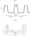
- FIGs. 8 to 11 are sectional views of barrier ribs of a PDP in accordance with a third embodiment.
- the PDP in accordance with the third embodiment is characterized in that upper and lower widths of the barrier ribs are different in order to reduce the second and third capacitances Cxy and Cxx.
- FIG. 8 is a sectional view of a vertical barrier rib 35a of the discharge cell and
- FIG. 9 is a sectional view of a horizontal barrier rib 35b of the discharge cell.
- the vertical barrier rib 35a is formed in the same direction as the address electrode (X), while the horizontal barrier rib 35b is formed in the same direction as the scan electrode (Y) and the sustain electrode (Z).
- the same reference numerals as those in the above-described embodiment are given to the substantially same elements in this embodiment, and repetitive descriptions will be omitted.
- vertical barrier ribs 35a separate each of R, G and B discharge cells, prevent a leakage of a discharge gas between discharge cells, and prevent influence of ultraviolet rays and visible light emitted from each discharge space on an adjacent cell.
- the process is easy with a wide vertical barrier rib 35a, but if the barrier rib is too wide, capacitance would be increased.
- the vertical barrier rib 35a has the upper width U1 of 40 ⁇ m ⁇ 55 ⁇ m and the lower width D1 of 60 ⁇ m ⁇ 90 ⁇ m to facilitate the barrier rib formation process as well as reduce panel capacitance.
- the lower width D1 of the vertical barrier rib 35a is larger by 1.4 times to 1.9 times than the upper width U1.
- this is not essential.
- the horizontal barrier ribs 35b separate discharge cells corresponding to upper and lower lines formed in a horizontal direction of the panel.
- the horizontal barrier ribs 35b separate the discharge cells corresponding to the horizontal line, so they have a larger width. Namely, the lower width D2 of the horizontal barrier rib is 160 ⁇ m ⁇ 200 ⁇ m while the upper width U2 of the horizontal barrier rib is 100 ⁇ m ⁇ 140 ⁇ m.
- the horizontal barrier rib 35b is formed such that its lower width D2 is larger by 1.6 times to 2 times than the upper width U2 thereof.
- this is not essential.
- FIG. 10 is a sectional view of the discharge cell in accordance with the third embodiment.
- a height (hh1) of the vertical barrier rib 35a is 130 ⁇ m or greater, and the horizontal barrier rib 35b also have the same height (hh1).
- a Pb-free barrier rib with a dielectric constant of 10 or lower can be used as the vertical barrier rib 35a and the horizontal barrier rib 35b.
- the phosphor layer 36 with the thickness (hh2) of 10 ⁇ m or smaller is formed on the lower dielectric layer 37 stacked on the address electrode (X) and on the barrier ribs 35a and 35b.
- Capacitance according to the upper and lower widths of the barrier rib, the height of the barrier rib and the thickness of the phosphor layer will be described with reference to [Table 2] and [Table 3] shown below.
- the second capacitance Cxx is reduced.
- a region where the scan electrode (Y) formed at the upper plate and the address electrode (X) formed at the lower plate overlap must be small.
- the area of the overlap portion (J) is preferably 14,000 ⁇ m 2 or smaller.
- the upper/lower plate electrode overlap portion (J) is formed not to overlap with the barrier ribs 35a and 35B whose upper and lower widths are different.
- the scan electrode (Y) and the sustain electrode (Z) of the upper plate are separated with a distance of 90 ⁇ m or longer therebetween, forming a long gap (T3) therebetween, and the width (T1) of each electrode is 200 ⁇ m or smaller.
- the address electrode (X) of the lower plate has the width (T2) of 80 ⁇ m or smaller.
- the barrier ribs can be formed according to any known techniques such as a screen printing method, an addition method, a photosensitive pasting method, an LTCCM (Low Temperature Cofired Ceramic on Metal) method, a sand blasting method, and the like.
- FIG. 12 is a plan view of a PDP in accordance with a fourth embodiment.
- the PDP in accordance with the fourth embodiment is characterized in that the width of the address electrode (X) crossing the scan electrode (Y) is larger than other portion thereof to reduce the second and third capacitances Cxx and Cxy.
- the address electrode (X) includes a protruding portion with a first width (T4) at a portion (J') thereof overlapping with the scan electrode (Y), while the other portion thereof has a second width (T5) smaller than the first width (T4).
- the first width (T4) of the address electrode (X) is 100 ⁇ m ⁇ 120 ⁇ m, while the second width (T5) thereof is 20 ⁇ m ⁇ 80 ⁇ m.
- the scan electrode (Y) and the sustain electrode (Z) are separated with a distance of 90 ⁇ m or longer therebetween, forming a long gap therebetween, and the width (T1) of each electrode is 200 ⁇ m or smaller.
- the long gap between the scan electrode (Y) and the sustain electrode (Z) improves the sustain discharge efficiency
- the increased width of the portion of the address electrode (X) overlapping with the scan electrode (Y) improves the address discharge efficiency
- the narrow width of the other portion of the address electrode not overlapping with the scan electrode (Y) reduces the second and third capacitances Cxx and Cxy.
Landscapes
- Physics & Mathematics (AREA)
- Engineering & Computer Science (AREA)
- Plasma & Fusion (AREA)
- Gas-Filled Discharge Tubes (AREA)
Abstract
Description
- The present invention relates to a plasma display panel (PDP). It more particularly relates to a PDP capable of reducing capacitance of a panel.
- A PDP is an apparatus in which discharge cells are formed between a rear substrate with barrier ribs formed thereon and a front substrate facing the rear substrate, and when an inert gas inside each discharge cell is discharged by a high frequency voltage, vacuum ultraviolet rays are generated to illuminate phosphor to thereby allow displaying of images.
- FIG. 1 is a perspective view showing the structure of a general prior art PDP, and FIG. 2 is a sectional view showing a discharge cell of the general PDP.
- First, discharge cells are formed by a plurality of
barrier ribs 24 separating a discharge space on arear substrate 18 facing afront substrate 10. - An address electrode X is formed on the
rear substrate 18, and a scan electrode Y and a sustain electrode Z are formed as a pair on thefront substrate 10. The address electrode X crosses the other electrodes Y and Z, and in this respect, therear substrate 18 in FIG. 2 is shown as having been rotated by 90° for the sake of explanation. - A
dielectric layer 22 for accumulating wall charges is formed on therear substrate 18 with the address electrode X formed thereon. - The
barrier ribs 24 are formed on thedielectric layer 22 to define a discharge space therebetween and prevent a leakage of ultraviolet rays and visible light generated by a discharge to an adjacent discharge cell.Phosphor 26 is coated on the surface of thedielectric layer 22 and on the surface of thebarrier ribs 24. - Because an inert gas is injected into the discharge space, the
phosphor 26 is excited by the ultraviolet rays generated during a gas discharge to generate one of red, green and blue visible light. - The scan electrode Y and the sustain electrode Z formed on the
front substrate 10 includetransparent electrodes bus electrodes dielectric layer 14 and aprotective film 16 are formed to cover the scan electrode Y and the sustain electrode Z. - The discharge cell with such a structure is selected by a facing discharge formed between the address electrode X and the scan electrode Y, and the discharge is sustained by a surface discharge between the scan electrode Y and the sustain electrode Z, to thus emit visible light.
- The scan electrode Y and the sustain electrode Z include the
transparent electrodes bus electrodes transparent electrodes transparent electrodes - FIG. 3 shows a frame of the general PDP.
- With reference to FIG. 3, in the plasma display panel, in order to represent gray levels of an image, one frame is divided into several sub-fields (SF1 to SF8) each having a different number of times of illumination and driven according to time division. Each sub-field (SF1~SF8) includes a reset period for initializing wall charges within the discharge cell, an address period for selecting a scan line and then selecting a discharge cell from the selected scan line, and a sustain period (S) for implementing a gray level according to the number of times that a sustain discharge occurs.
- Gray levels implemented in the sub-fields including the reset period, the address period and the sustain period are accumulated during one frame, and in case where an image is represented with 256 gray levels, as shown in FIG. 3, a frame period (16.67ms) corresponding to 1/60 seconds is divided into eight sub-fields (SF1 to SF8) and each sub-field represents 2n (n=0, 1, 2, 3, 4, 5, 6, 7) gray levels.
- Having characteristics of storing energy according to electric field and inducing a current by voltage variation, the discharge cells of the PDP for displaying images can be equivalent to a capacitor, and capacitance of the panel affects reactive power and the discharge efficiency.
- In detail, as for the relationship between the capacitance of the panel and the reactive power and the discharge efficiency, under the condition that a load is high like a full white pattern during the sustain period, discharge power is greater than reactive power, whereas under the practical condition that a load is about 20% or smaller like a general TV broadcast program or a movie, the reactive power is greater than the discharge power. In such a practical condition, more sustain pulses in the full white condition are applied to emphasize luminance than under the practical condition, so in order to enhance the discharge efficiency with the same power consumption, reactive power according to switching must be reduced during the sustain period.
- In addition, when a specific input pattern that ON/OFF is repeated in up/down/left/right directions is inputted, the reactive power is increased during the address period, causing problems of an increase in power consumption, waveform distortion, an erroneous discharge, and IC heating.
- Especially, in case of a panel of a HD class or higher employing single scanning, the address period is lengthened double compared with a case where dual scanning is employed and the number of times of switching of the address voltage is also increased double, further increasing reactive power consumption during the address period.
- In an effort to reduce such reactive power, in the related art, a discharge gas such as high Xe is used to improve the discharge efficiency. In this case, however, if the discharge gas is contained by 10% or more, a sustain voltage or the address voltage are inevitably increased together to rather increase reactive power, failing to improve the discharge efficiency under the practical conditions.
- Therefore, designing for reducing capacitance Cyz of an upper plate, capacitance Cxx of a lower plate and upper/lower plate panel capacitance Cxy is necessary to reduce the reactive power during the sustain period and the address period and enhance the discharge efficiency.
- The present invention seeks to provide an improved plasma display apparatus.
- A first aspect of the invention provides a plasma display panel (PDP) including an upper plate and a lower plate. The upper plate includes a scan electrode and a sustain electrode, and the lower plate includes an address electrode. The upper plate or the lower plate is formed to have a dielectric constant of 10 or lower.
- The scan electrode and the sustain electrode may be arranged to be symmetrical with a scan electrode and a sustain electrode of an adjacent discharge cell.
- The upper plate may additionally include an upper dielectric layer stacked on the scan electrode and the sustain electrode, and the upper dielectric layer may have a dielectric constant of 10 or lower and the thickness of 35µm or smaller.
- The scan electrode and the sustain electrode may be formed of a transparent electrode and a metal bus electrode, respectively, and the transparent electrodes may be formed to be separated by a distance of 90µm therebetween and may have a width of 200µm or smaller.
- Another aspect of the invention provides a plasma display panel (PDP) including an upper plate and a lower plate as coupled. At least one or more electrodes are formed on the upper and lower plates. An upper dielectric layer stacked on the electrode of the upper plate is formed such that a portion thereof overlapping with the electrode is thicker than a portion that does not overlap with the electrode.
- The upper dielectric layer having the portions each with a different thickness may have a dielectric constant of 10 or lower, and the thickness of the portion overlapping with the electrode may be 35µm or smaller and the thickness of the portion which does not overlap with the electrode may be 10µm or smaller.
- Another aspect of the invention provides a plasma display panel (PDP) including: an upper plate and a lower plate. The upper plate includes a scan electrode and a sustain electrode formed in a first direction. The lower plate includes an address electrode formed in a second direction that crosses the first direction, and vertical barrier ribs formed in the second direction to separate R, G and B pixel discharge cells and horizontal barrier ribs separating a panel line in the first direction. The horizontal and vertical barrier ribs are formed such that their lower width is larger than their upper width.
- The lower width of the horizontal barrier rib may be larger by 1.6 times to 2 times than the upper width thereof, while the lower width of the vertical barrier rib may be larger by 1.4 times to 1.9 times than the upper width.
- The horizontal and vertical barrier ribs may have a height of 120µm or larger, and may have a dielectric constant of 10 or lower or may be formed as Pb-free barrier ribs having a low dielectric constant.
- A phosphor layer may be formed with a thickness of 10µm or smaller on a lower dielectric layer stacked on the address electrode and on the barrier rib.
- The scan electrode and the sustain electrode may be formed on the upper plate such that an area thereof overlapping with the address electrode formed on the lower plate is 14,000µm2 or smaller, and a portion where the upper and lower plates electrodes overlap does not overlap with the barrier rib. The scan electrode and the sustain electrode may have a width of 200µm or smaller, and the address electrode of the lower plate may have a width of 80µm or smaller.
- Another aspect of the invention provides a plasma display panel (PDP) including an upper plate and a lower plate as coupled. The upper plate includes a scan electrode and a sustain electrode and the lower plate includes an address electrode. The address electrode has a protruding portion with a first width overlapping with the scan electrode, and other portion, than the protruding portion, of the address electrode has a second width smaller than the first width.
- The area of the address electrode overlapping with the scan electrode by the protruding portion may be 14,000µm2 or smaller and need not overlap with barrier ribs formed on the lower plate.
- The first width of the address electrode may be 100µm to 120µm, and the second width thereof may be 20µm to 80µm.
- Embodiments of the invention will now be described by way of non-limiting example only, with reference to the drawings in which:
- FIG. 1 is a perspective view showing a discharge cell of a general plasma display panel (PDP).
- FIG. 2 is a sectional view showing the discharge cell of the general PDP.
- FIG. 3 shows the construction of a frame for implementing 256 gray levels.
- FIG. 4 is a view equivalently showing capacitance of upper and lower plates of the general PDP.
- FIG. 5 is a perspective view of a PDP in accordance with a first embodiment of the present invention.
- FIGs. 6 and 7 are sectional views showing a PDP in accordance with a second embodiment of the present invention.
- FIG. 8 is a sectional view of vertical barrier ribs of the PDP in accordance with a third embodiment of the present invention.
- FIG. 9 is a sectional view of horizontal barrier ribs of the PDP in accordance with a third embodiment of the present invention.
- FIG. 10 is a sectional view of a discharge cell of the PDP in accordance with the third embodiment of the present invention.
- FIG. 11 shows the structure of an electrode of the PDP in accordance with the third embodiment of the present invention.
- FIG. 12 shows the structure of an electrode of the PDP in accordance with a fourth embodiment of the present invention.
- The embodiments are given merely by way of examples of PDPs in accordance with the invention, and the invention can be performed in ways other than those described in the present description.
- The first to fourth embodiments of the present invention will be described with reference to FIGs. 4 to 12.
- With reference to FIG. 4, a first capacitance Cyz is formed between a scan electrode (Y) and a sustain electrode (Z) on an
upper plate 20 of the PDP in accordance with the present invention. Ascan drive IC 52 and a sustaindrive IC 53 for supplying a drive signal are connected with the scan electrode (Y) and the sustain electrode (Z), respectively. - A second capacitance Cxx is formed between address electrodes X1 and X2 at a
lower plate 28 of the panel, and anaddress drive IC 62 supplies a drive signal required for the address electrodes X1 and X2. - A third capacitance Cxy is formed between the scan electrode Y of the
upper plate 20 and the address electrode X1 of thelower plate 28. - With reference to FIG. 5, the PDP in accordance with the first embodiment is characterized in that the
upper plate 20 and thelower plate 28 have a low dielectric constant (Lε) of 10 or lower in order to reduce the first to third capacitances Cyz, Cxx and Cxy. - The scan electrode (Y) and the sustain electrode (Z) are formed on the
upper plate 20, and the address electrode (X) is formed on thelower plate 28. A discharge space is formed at a crossing of the scan electrode (Y), the sustain electrode (Z) and the address electrode (X). - In this embodiment, the scan electrode (Y) and the sustain electrode (Z) of a discharge cell are arranged to be symmetrical with the scan electrode (Y) and the sustain electrode (Z) of an adjacent discharge cell. However, this is not essential.
- In such a (YZ|ZY) electrode disposition structure, since the same electrodes (Z|Z) are disposed between adjacent discharge cells, an additional electric field is not formed and thus the first capacitance Cyz can be reduced compared with a (YZ|YZ) electrode disposition structure.
- In order to reduce capacitance of the panel, the upper and
lower plates lower plates - The scan electrode (Y) and the sustain electrode (Z) include a
transparent electrode 22 and ametal bus electrode 21, respectively, and adielectric layer 23 covering the electrodes and aprotective film 24 are stacked thereon. - In this embodiment, the width of the transparent electrode is 200µm or smaller and the transparent electrodes are separated with a long gap of 90µm or larger therebetween. However, this is not essential. The longer the gap between the electrodes Y and Z of the
upper plate 20 is, the more the first capacitance Cyz is reduced. - A
lower dielectric layer 27 is stacked on thelower plate 28, andbarrier ribs 25 for separating the discharge cell are formed thereon.Phosphor 26 is coated on a surface of the lowerdielectric layer 27 and thebarrier ribs 25. - The
upper dielectric layer 23 of theupper plate 20 and the lowerdielectric layer 27 of thelower plate 28 also have a dielectric constant of 10 or lower, and since the first to third capacitances Cyz, Cxx and Cxy are reduced as the thickness of the upper and lowerdielectric layers - In the first embodiment, by lowering the dielectric constant of the upper and
lower plates 

- With reference to FIG. 4, when the dielectric constant of the
upper plate 20 is lowered, capacitance of the upper plate is reduced according to equation (1) and a current passing through thescan drive IC 52 and the sustaindrive IC 53 is also reduced according to equation (2). In addition, as the drive current is reduced, power consumption at each of thedrive ICs - Likewise, when the dielectric constant of the
lower plate 28 is lowered, capacitance of the lower plate is reduced according to equation (1) and a current passing through theaddress drive IC 62 and power consumption are reduced according to equation (2). - The dielectric constant of the
upper plate 20 or thelower plate 28 can be also lowered in a different method. That is, the content of alkali metal having conductivity contained in the upper plate or the lower plate can be reduced to lower the dielectric constant. - In addition, because dielectric constant is increased as dielectric strength or a working voltage of glass is increased, it is preferred that the
upper plate 20 or thelower plate 28 is fabricated to have small dielectric strength and a small working voltage. However, this is not essential to the invention in its broadest aspect. - FIGs. 6 and 7 are sectional views showing a PDP in accordance with a second embodiment, in which the upper plate is shown as having been rotated by 90°.
- The PDP in accordance with the second embodiment is characterized in that, in order to reduce the first capacitance Cyz, an
upper dielectric layer 33a has a thickness (h) of 10µm or smaller, or a thickness (h2) of portions of anupper dielectric layer 33b overlapping with the scan electrode (Y) and the sustain electrode (Z) and a thickness (h1) of other portion of theupper dielectric layer 33b are different. - The structure of the discharge cell will now be described with reference to FIGs. 6 and 7. As shown, the scan electrode (Y) and the sustain electrode (Z) are formed on an
upper plate 30, and the address electrode (X) is formed on alower plate 38. The scan electrode (Y) and the sustain electrode (Z) include atransparent electrode 31 and ametal bus electrode 32 having a smaller line width than thetransparent electrode 31 and formed on one portion of thetransparent electrode 31, respectively. - Upper
dielectric layers protective films upper plate 30. - On the
lower plate 38, there are sequentially formed a lowerdielectric layer 37 and abarrier rib 35, and aphosphor layer 36 is coated on a surface of the lowerdielectric layer 37 and thebarrier rib 35. - As shown in FIG. 6, the thickness (h) of the
upper dielectric layer 33a is 10µ or smaller, and the smaller the thickness of the upper dielectric layer, the more capacitance of the panel is reduced. - In this respect, however, if the thickness (h) of the
upper dielectric layer 33a is too small, the panel capacitance could be reduced, but wall charges generated according to the plasma discharge are not sufficiently formed. Thus, in order to solve such a problem, the PDP adopting a differential dielectric layer as shown in FIG. 7 is proposed. - With reference to FIG. 7, the same reference numerals as those in the above-described embodiment are given to the substantially same elements in this embodiment, and repetitive descriptions will be omitted.
- In this embodiment, the
upper dielectric layer 33b is formed to have a different thickness in different locations. Namely, the thickness (h2) of the portions of theupper dielectric layer 33b which overlap with the scan electrode (Y) and the sustain electrode (Z) is larger than the thickness (h1) of the other portion of theupper dielectric layer 33b. - The dielectric constant of the
upper dielectric layer 33b according to each thickness will be described with reference to [Table 1] shown below.[Table 1] First capacitance (Cyz) Thickness of dielectric (h2) Thickness of Dielectric (h1) Dielectric constant A 40µm 0µm 11 B 35µm 5µm 10 C 30µm 10µm 9 - As shown in [Table 1], in order to have the dielectric constant of 10 or lower, the
upper dielectric layer 33b is formed such that the portion thereof overlapping with the upper electrodes Y and Z has the thickness (h2) of 35µm or smaller and the other portion of theupper dielectric layer 33b is set to have the thickness (h1) of about 10µm or smaller. - Accordingly, sufficient wall charges can be formed at the portion of the
upper dielectric layer 33b with the larger thickness (h2) according to the plasma discharge, and the first capacitance Cyz at the portion of theupper dielectric layer 33b with the smaller thickness (h1) can be reduced. - FIGs. 8 to 11 are sectional views of barrier ribs of a PDP in accordance with a third embodiment. The PDP in accordance with the third embodiment is characterized in that upper and lower widths of the barrier ribs are different in order to reduce the second and third capacitances Cxy and Cxx.
- FIG. 8 is a sectional view of a
vertical barrier rib 35a of the discharge cell and FIG. 9 is a sectional view of ahorizontal barrier rib 35b of the discharge cell. - The
vertical barrier rib 35a is formed in the same direction as the address electrode (X), while thehorizontal barrier rib 35b is formed in the same direction as the scan electrode (Y) and the sustain electrode (Z). The same reference numerals as those in the above-described embodiment are given to the substantially same elements in this embodiment, and repetitive descriptions will be omitted. - With reference to FIG. 8,
vertical barrier ribs 35a separate each of R, G and B discharge cells, prevent a leakage of a discharge gas between discharge cells, and prevent influence of ultraviolet rays and visible light emitted from each discharge space on an adjacent cell. - Generally, the process is easy with a wide
vertical barrier rib 35a, but if the barrier rib is too wide, capacitance would be increased. Thus, in this embodiment, thevertical barrier rib 35a has the upper width U1 of 40µm~55µm and the lower width D1 of 60µm~90µm to facilitate the barrier rib formation process as well as reduce panel capacitance. - That is, in the present embodiment, the lower width D1 of the
vertical barrier rib 35a is larger by 1.4 times to 1.9 times than the upper width U1. However, this is not essential. - With reference to FIG. 9, the
horizontal barrier ribs 35b separate discharge cells corresponding to upper and lower lines formed in a horizontal direction of the panel. - Unlike the
vertical barrier ribs 35a separating the R, G and B sub-discharge cells, thehorizontal barrier ribs 35b separate the discharge cells corresponding to the horizontal line, so they have a larger width. Namely, the lower width D2 of the horizontal barrier rib is 160µm~200µm while the upper width U2 of the horizontal barrier rib is 100µm~140µm. - In this manner, in the present embodiment, the
horizontal barrier rib 35b is formed such that its lower width D2 is larger by 1.6 times to 2 times than the upper width U2 thereof. However, this is not essential. - FIG. 10 is a sectional view of the discharge cell in accordance with the third embodiment. In this embodiment, a height (hh1) of the
vertical barrier rib 35a is 130µm or greater, and thehorizontal barrier rib 35b also have the same height (hh1). As thevertical barrier rib 35a and thehorizontal barrier rib 35b, a Pb-free barrier rib with a dielectric constant of 10 or lower can be used. - The
phosphor layer 36 with the thickness (hh2) of 10µm or smaller is formed on the lowerdielectric layer 37 stacked on the address electrode (X) and on thebarrier ribs - Capacitance according to the upper and lower widths of the barrier rib, the height of the barrier rib and the thickness of the phosphor layer will be described with reference to [Table 2] and [Table 3] shown below.
[Table 2] Second capacitance (Cxx) Upper/lower width of vertical barrier rib Upper/lower width of horizontal barrier rib Thickness of phosphor layer Dielectric constant of barrier rib A 60/110 180/300 14 12 B 55/90 120/200 10 10 C 50/70 60/120 6 8 [Table 3] Third capacitance (Cxy) Upper/lower width of vertical barrier rib Upper/lower width of horizontal barrier rib Thickness of phosphor layer Height of barrier rib Dielectric constant of barrier rib A 60/110 180/300 14 120 12 B 55/90 120/200 10 130 10 C 50/70 60/120 6 140 8 - As noted in [Table 2], as the width of the barrier rib becomes small or the thickness of the phosphor layer becomes small, or as the dielectric constant of the barrier rib is reduced, the second capacitance Cxx is reduced.
- As noted in [Table 3], as the width of the barrier rib becomes small and the height of the barrier rib is increased, the distance between the electrodes of the upper and lower plates becomes longer and thus the third capacitance Cxy is reduced. Also, as the thickness of the phosphor layer becomes small and the dielectric constant of the barrier rib is reduced, the third capacitance Cxy is reduced.
- In particular, in order to reduce the third capacitance Cxy formed between the upper and lower plates, as shown in FIG. 11, a region where the scan electrode (Y) formed at the upper plate and the address electrode (X) formed at the lower plate overlap must be small. When the region where the electrodes overlap is an upper/lower plate electrode overlap portion (J), the area of the overlap portion (J) is preferably 14,000µm2 or smaller.
- The upper/lower plate electrode overlap portion (J) is formed not to overlap with the
barrier ribs 35a and 35B whose upper and lower widths are different. - The scan electrode (Y) and the sustain electrode (Z) of the upper plate are separated with a distance of 90µm or longer therebetween, forming a long gap (T3) therebetween, and the width (T1) of each electrode is 200µm or smaller. At this time, the address electrode (X) of the lower plate has the width (T2) of 80µm or smaller.
- In this manner, in the third embodiment, by forming the
vertical barrier rib 35a and thehorizontal barrier rib 35b such that they have the different upper and lower widths, the second and third capacitances Cxx and Cxy can be reduced. As for formation of the barrier ribs, the barrier ribs can be formed according to any known techniques such as a screen printing method, an addition method, a photosensitive pasting method, an LTCCM (Low Temperature Cofired Ceramic on Metal) method, a sand blasting method, and the like. - FIG. 12 is a plan view of a PDP in accordance with a fourth embodiment. The PDP in accordance with the fourth embodiment is characterized in that the width of the address electrode (X) crossing the scan electrode (Y) is larger than other portion thereof to reduce the second and third capacitances Cxx and Cxy.
- The same reference numerals as those in the above-described embodiment are given to the substantially same elements in this embodiment, and repetitive descriptions will be omitted.
- In the fourth embodiment, the address electrode (X) includes a protruding portion with a first width (T4) at a portion (J') thereof overlapping with the scan electrode (Y), while the other portion thereof has a second width (T5) smaller than the first width (T4).
- In this case, since the area overlapping with the scan electrode (Y) extends by the protruding portion of the address electrode (X), an address discharge can occur stably, and since the second width (T5) of the address electrode is narrow to make the area of the overlap portion (J') 14,000µm2 or smaller, the second and third capacitances Cxx and Cxy can be reduced.
- At this time, the first width (T4) of the address electrode (X) is 100µm~120µm, while the second width (T5) thereof is 20µm~80µm.
- In addition, in the fourth embodiment, the scan electrode (Y) and the sustain electrode (Z) are separated with a distance of 90µm or longer therebetween, forming a long gap therebetween, and the width (T1) of each electrode is 200µm or smaller.
- Accordingly, the long gap between the scan electrode (Y) and the sustain electrode (Z) improves the sustain discharge efficiency, and the increased width of the portion of the address electrode (X) overlapping with the scan electrode (Y) improves the address discharge efficiency, and the narrow width of the other portion of the address electrode not overlapping with the scan electrode (Y) reduces the second and third capacitances Cxx and Cxy.
- As the present invention may be embodied in several forms without departing from the essential characteristics thereof, it should also be understood that the above-described embodiments are not limited by any of the details of the foregoing description, unless otherwise specified, but rather should be construed broadly within its scope as defined in the appended claims, and therefore all changes and modifications that fall within the metes and bounds of the claims, or equivalence of such metes and bounds are therefore intended to be embraced by the appended claims.
Claims (25)
- A plasma display panel comprising:an upper plate comprised of a scan electrode and a sustain electrode;a lower plate comprised of an address electrode,wherein the upper or lower plate has a dielectric constant of 10 or lower.
- The panel of claim 1, wherein scan and sustain electrodes of one discharge cell are arranged to be symmetrical with scan and sustain electrodes of an adjacent discharge cell.
- The panel of claim 1 or 2, wherein the upper plate comprises an upper dielectric layer stacked on the scan electrode and the sustain electrode, and the upper dielectric layer has a dielectric constant of 10 or lower.
- The panel of claim 3, wherein the upper dielectric layer has a thickness of 35µm or smaller.
- The panel of any one of claims 1 to 4, wherein the scan electrode and the sustain electrode are formed of a transparent electrode and a metal bus electrode, respectively, and the transparent electrodes are separated with a distance of 90µm therebetween.
- The panel of claim 5, wherein the width of the transparent electrodes is 200µm or smaller.
- A plasma display panel comprising:an upper plate; anda lower plate facing the upper plate,the upper plate and the lower plate being coupled,wherein at least one or more electrodes are formed on the upper and lower plates, and an upper dielectric layer is stacked on the electrode of the upper plate such that a thickness of a portion of the upper dielectric layer overlapping with the electrode is larger than that of a portion thereof which does not overlap with the electrode.
- The panel of claim 7, wherein the upper dielectric layer has a dielectric constant of 10 or lower.
- The panel of claim 7 or 8, wherein the thickness of the upper dielectric layer is 35µm or smaller.
- The panel of any one of claims 7 to 9, wherein the portion of the upper dielectric layer overlapping with the electrode has the thickness of 35µm or smaller, and the portion thereof which does not overlap with the electrode has the thickness of 10µm or smaller.
- A plasma display panel comprising:an upper plate comprised of a scan electrode and a sustain electrode formed in a first direction; anda lower plate comprised of an address electrode formed in a second direction crossing the first direction, and a vertical barrier rib formed in the second direction to separate R, G and B pixel discharge cells and a horizontal barrier rib separating a panel line in the first direction,wherein the horizontal and vertical barrier ribs have a lower width larger than the upper width thereof.
- The panel of claim 11, wherein the lower width of the horizontal barrier rib is larger by 1.6 times to 2 times than the upper width thereof.
- The panel of claim 11 or 12, wherein the lower width of the vertical barrier rib is larger by 1.4 times to 1.9 times than the upper width thereof.
- The panel of claim 11, 12 or 13 wherein the horizontal or vertical barrier rib has a height of 120µm or larger.
- The panel of any one of claims 11 to 14, wherein the horizontal or vertical barrier rib has a dielectric constant of 10 or lower.
- The panel of any one of claims 11 to 15, wherein the horizontal or vertical barrier rib is a Pb-free barrier rib.
- The panel of any one of claims 11 to 16, wherein a phosphor layer with a thickness of 10µm or smaller is formed on the lower dielectric layer stacked on the address electrode and on the barrier rib formed at the lower plate.
- The panel of any one of claims 11 to 17, wherein an upper and lower plate electrode overlap portion where the scan electrode and the sustain electrode of the upper plate and the address electrode of the lower plate overlap has an area of 14,000µm2.
- The panel of claim 18, wherein the upper and lower plate electrode overlap portion does not overlap with a portion of the barrier rib.
- The panel of claim 18 or 19, wherein when the scan electrode and the sustain electrode of the upper plate are formed with a width of 200µm or smaller, the address electrode of the lower plate is formed with a width of 80µm or smaller.
- A plasma display panel comprising:an upper plate comprised of a scan electrode and a sustain electrode; anda lower plate comprised of an address electrode,wherein the address electrode comprises a protruding portion with a first width overlapping with the scan electrode, other portion, than the protruding portion, of the address electrode having a second width smaller than the first width.
- The panel of claim 21, wherein the protruding portion of the address electrode has the area of 14,000µm2 or smaller.
- The panel of claim 21 or 22, wherein the protruding portion of the address electrode does not overlap with a barrier rib formed at the lower plate.
- The panel of claim 21, 22 or 23 wherein the first width of the address electrode is 100µm~120µm and the second width thereof is 20µm~80µm.
- The panel of any one of claims 21 to 24, wherein a phosphor layer with the thickness of 10µm or smaller is formed on the lower dielectric layer stacked on the address electrode and on the barrier rib of the lower plate.
Applications Claiming Priority (3)
| Application Number | Priority Date | Filing Date | Title |
|---|---|---|---|
| KR1020040096625A KR100697013B1 (en) | 2004-11-23 | 2004-11-23 | Plasma Display Panel |
| KR1020040100050A KR100697006B1 (en) | 2004-12-01 | 2004-12-01 | Plasma Display Panel |
| KR1020040103862A KR20060065126A (en) | 2004-12-09 | 2004-12-09 | Plasma display panel |
Publications (2)
| Publication Number | Publication Date |
|---|---|
| EP1696458A2 true EP1696458A2 (en) | 2006-08-30 |
| EP1696458A3 EP1696458A3 (en) | 2008-05-07 |
Family
ID=36583008
Family Applications (1)
| Application Number | Title | Priority Date | Filing Date |
|---|---|---|---|
| EP05257225A Withdrawn EP1696458A3 (en) | 2004-11-23 | 2005-11-23 | Plasma display panel |
Country Status (3)
| Country | Link |
|---|---|
| US (1) | US20060125398A1 (en) |
| EP (1) | EP1696458A3 (en) |
| JP (1) | JP2006147584A (en) |
Cited By (1)
| Publication number | Priority date | Publication date | Assignee | Title |
|---|---|---|---|---|
| US9558254B2 (en) | 2010-12-20 | 2017-01-31 | Ford Global Technologies, Llc | Automatic wireless device data maintenance |
Families Citing this family (5)
| Publication number | Priority date | Publication date | Assignee | Title |
|---|---|---|---|---|
| KR100755306B1 (en) * | 2005-12-12 | 2007-09-05 | 엘지전자 주식회사 | Plasma Display Panel |
| KR100730194B1 (en) * | 2005-12-30 | 2007-06-19 | 삼성에스디아이 주식회사 | Plasma display panel |
| JP4089732B2 (en) * | 2006-02-14 | 2008-05-28 | 松下電器産業株式会社 | Plasma display panel |
| KR100839668B1 (en) * | 2007-04-09 | 2008-06-19 | 엘지전자 주식회사 | Plasma display panel |
| KR20090002982A (en) * | 2007-07-05 | 2009-01-09 | 엘지전자 주식회사 | Plasma display panel |
Citations (4)
| Publication number | Priority date | Publication date | Assignee | Title |
|---|---|---|---|---|
| JPH09120777A (en) * | 1995-10-26 | 1997-05-06 | Hitachi Ltd | Electrode structure of plasma display panel |
| EP1187166A2 (en) * | 2000-09-06 | 2002-03-13 | Fujitsu Hitachi Plasma Display Limited | Plasma display panel and method for manufacturing the same |
| JP2003197110A (en) * | 2001-12-26 | 2003-07-11 | Matsushita Electric Ind Co Ltd | Plasma display panel |
| US20040017155A1 (en) * | 2002-07-23 | 2004-01-29 | Fujitsu Limited | Substrate assembly for gas discharge panel, process for manufacturing the same, and gas discharge panel |
Family Cites Families (24)
| Publication number | Priority date | Publication date | Assignee | Title |
|---|---|---|---|---|
| US6787995B1 (en) * | 1992-01-28 | 2004-09-07 | Fujitsu Limited | Full color surface discharge type plasma display device |
| KR19980065367A (en) * | 1996-06-02 | 1998-10-15 | 오평희 | Backlight for LCD |
| DE69708822T2 (en) * | 1996-09-18 | 2002-04-11 | Matsushita Electric Ind Co Ltd | Manufacturing method of a plasma display panel suitable for tiny cell structures, plasma display panel, and device for displaying the plasma display panel |
| US6479932B1 (en) * | 1998-09-22 | 2002-11-12 | Nec Corporation | AC plasma display panel |
| KR100322071B1 (en) * | 1999-03-31 | 2002-02-04 | 김순택 | Plasma display devie and method of manufacture the same |
| US6411035B1 (en) * | 1999-05-12 | 2002-06-25 | Robert G. Marcotte | AC plasma display with apertured electrode patterns |
| US6680573B1 (en) * | 1999-07-26 | 2004-01-20 | Lg Electronics Inc. | Plasma display panel with improved illuminance |
| KR100878405B1 (en) * | 2000-01-25 | 2009-01-13 | 파나소닉 주식회사 | Gas discharge panel |
| WO2001071761A1 (en) * | 2000-03-24 | 2001-09-27 | Matsushita Electric Industrial Co., Ltd. | Plasma display panel and method for its manufacure |
| JP2002075220A (en) * | 2000-08-28 | 2002-03-15 | Pioneer Electronic Corp | Plasma display panel |
| JP2002117756A (en) * | 2000-10-05 | 2002-04-19 | Fujitsu Ltd | Method for manufacturing original die for barrier rib transfer and barrier rib forming method |
| EP1361593A4 (en) * | 2001-01-17 | 2008-06-04 | Matsushita Electric Ind Co Ltd | Plasma display panel and its manufacturing method |
| JP3389243B1 (en) * | 2001-07-03 | 2003-03-24 | 松下電器産業株式会社 | Plasma display panel and method of manufacturing the same |
| US6910937B2 (en) * | 2001-07-30 | 2005-06-28 | Sony Corporation | Method for forming fine barrier, method for fabricating planar display and abrasive for blast |
| WO2003032356A1 (en) * | 2001-10-02 | 2003-04-17 | Noritake Co., Limited | Gas discharge display device and its manufacturing method |
| US6897564B2 (en) * | 2002-01-14 | 2005-05-24 | Plasmion Displays, Llc. | Plasma display panel having trench discharge cells with one or more electrodes formed therein and extended to outside of the trench |
| US7288892B2 (en) * | 2002-03-12 | 2007-10-30 | Board Of Trustees Of The Leland Stanford Junior University | Plasma display panel with improved cell geometry |
| US6853144B2 (en) * | 2002-06-28 | 2005-02-08 | Matsushita Electric Industrial Co., Ltd | Plasma display with split electrodes |
| JP2004143398A (en) * | 2002-08-29 | 2004-05-20 | Konica Minolta Holdings Inc | Zinc silicate phosphor, its production method and plasma display panel |
| EP1435639B1 (en) * | 2003-01-02 | 2010-07-28 | Samsung SDI Co., Ltd. | Plasma display panel |
| JP2004251950A (en) * | 2003-02-18 | 2004-09-09 | Fuji Xerox Co Ltd | Rib for use in image display medium, method for manufacturing the same, and image display medium using the same |
| US7208876B2 (en) * | 2003-07-22 | 2007-04-24 | Samsung Sdi Co., Ltd. | Plasma display panel |
| KR100528919B1 (en) * | 2003-08-18 | 2005-11-15 | 삼성에스디아이 주식회사 | Plasma dispaly panel reduced outdoor daylight reflection |
| US7288013B2 (en) * | 2003-10-31 | 2007-10-30 | 3M Innovative Properties Company | Method of forming microstructures on a substrate and a microstructured assembly used for same |
-
2005
- 2005-11-22 JP JP2005337812A patent/JP2006147584A/en active Pending
- 2005-11-22 US US11/284,003 patent/US20060125398A1/en not_active Abandoned
- 2005-11-23 EP EP05257225A patent/EP1696458A3/en not_active Withdrawn
Patent Citations (4)
| Publication number | Priority date | Publication date | Assignee | Title |
|---|---|---|---|---|
| JPH09120777A (en) * | 1995-10-26 | 1997-05-06 | Hitachi Ltd | Electrode structure of plasma display panel |
| EP1187166A2 (en) * | 2000-09-06 | 2002-03-13 | Fujitsu Hitachi Plasma Display Limited | Plasma display panel and method for manufacturing the same |
| JP2003197110A (en) * | 2001-12-26 | 2003-07-11 | Matsushita Electric Ind Co Ltd | Plasma display panel |
| US20040017155A1 (en) * | 2002-07-23 | 2004-01-29 | Fujitsu Limited | Substrate assembly for gas discharge panel, process for manufacturing the same, and gas discharge panel |
Cited By (1)
| Publication number | Priority date | Publication date | Assignee | Title |
|---|---|---|---|---|
| US9558254B2 (en) | 2010-12-20 | 2017-01-31 | Ford Global Technologies, Llc | Automatic wireless device data maintenance |
Also Published As
| Publication number | Publication date |
|---|---|
| EP1696458A3 (en) | 2008-05-07 |
| JP2006147584A (en) | 2006-06-08 |
| US20060125398A1 (en) | 2006-06-15 |
Similar Documents
| Publication | Publication Date | Title |
|---|---|---|
| US20070114924A1 (en) | Plasma display panel | |
| EP1696458A2 (en) | Plasma display panel | |
| US20030227427A1 (en) | Plasma display panel | |
| US7605538B2 (en) | Plasma display panel | |
| US20060176247A1 (en) | Plasma display apparatus and driving method thereof | |
| US7687994B2 (en) | Plasma display panel (PDP) | |
| KR100501981B1 (en) | Plasma display panel | |
| US7928931B2 (en) | Plasma display apparatus | |
| CN1805102B (en) | Plasma display apparatus | |
| CN1773662B (en) | Plasma display apparatus | |
| US20040189202A1 (en) | Plasma display panel | |
| KR100549667B1 (en) | Plasma display panel | |
| KR100505984B1 (en) | Plasma display panel | |
| KR100962809B1 (en) | Plasma display device | |
| KR100613013B1 (en) | Plasma Display Panel | |
| US20070216606A1 (en) | Plasma display panel driving | |
| US20060097638A1 (en) | Plasma display panel | |
| KR100634686B1 (en) | Plasma Display Panel Including Electrode | |
| EP1696459B1 (en) | Plasma display panel | |
| US7759870B2 (en) | Plasma display panel (PDP) | |
| KR100626071B1 (en) | Plasma display panel | |
| KR100615333B1 (en) | Plasma display panel | |
| US20070057633A1 (en) | Plasma display panel | |
| KR20060034156A (en) | Plasma display panel | |
| US20100149154A1 (en) | Energy recovery circuit |
Legal Events
| Date | Code | Title | Description |
|---|---|---|---|
| PUAI | Public reference made under article 153(3) epc to a published international application that has entered the european phase |
Free format text: ORIGINAL CODE: 0009012 |
|
| 17P | Request for examination filed |
Effective date: 20051205 |
|
| AK | Designated contracting states |
Kind code of ref document: A2 Designated state(s): AT BE BG CH CY CZ DE DK EE ES FI FR GB GR HU IE IS IT LI LT LU LV MC NL PL PT RO SE SI SK TR |
|
| AX | Request for extension of the european patent |
Extension state: AL BA HR MK YU |
|
| PUAL | Search report despatched |
Free format text: ORIGINAL CODE: 0009013 |
|
| AK | Designated contracting states |
Kind code of ref document: A3 Designated state(s): AT BE BG CH CY CZ DE DK EE ES FI FR GB GR HU IE IS IT LI LT LU LV MC NL PL PT RO SE SI SK TR |
|
| AX | Request for extension of the european patent |
Extension state: AL BA HR MK YU |
|
| 17Q | First examination report despatched |
Effective date: 20080825 |
|
| AKX | Designation fees paid |
Designated state(s): DE FR GB NL |
|
| STAA | Information on the status of an ep patent application or granted ep patent |
Free format text: STATUS: THE APPLICATION IS DEEMED TO BE WITHDRAWN |
|
| 18D | Application deemed to be withdrawn |
Effective date: 20120605 |