EP1754995B1 - Methods for achieving improved color in microencapsulted electrophoretic devices - Google Patents
Methods for achieving improved color in microencapsulted electrophoretic devices Download PDFInfo
- Publication number
- EP1754995B1 EP1754995B1 EP06022456A EP06022456A EP1754995B1 EP 1754995 B1 EP1754995 B1 EP 1754995B1 EP 06022456 A EP06022456 A EP 06022456A EP 06022456 A EP06022456 A EP 06022456A EP 1754995 B1 EP1754995 B1 EP 1754995B1
- Authority
- EP
- European Patent Office
- Prior art keywords
- electrode
- display
- particles
- electrodes
- capsule
- Prior art date
- Legal status (The legal status is an assumption and is not a legal conclusion. Google has not performed a legal analysis and makes no representation as to the accuracy of the status listed.)
- Expired - Lifetime
Links
Images


Classifications
-
- B—PERFORMING OPERATIONS; TRANSPORTING
- B41—PRINTING; LINING MACHINES; TYPEWRITERS; STAMPS
- B41J—TYPEWRITERS; SELECTIVE PRINTING MECHANISMS, i.e. MECHANISMS PRINTING OTHERWISE THAN FROM A FORME; CORRECTION OF TYPOGRAPHICAL ERRORS
- B41J3/00—Typewriters or selective printing or marking mechanisms characterised by the purpose for which they are constructed
- B41J3/407—Typewriters or selective printing or marking mechanisms characterised by the purpose for which they are constructed for marking on special material
- B41J3/4073—Printing on three-dimensional objects not being in sheet or web form, e.g. spherical or cubic objects
-
- H—ELECTRICITY
- H10—SEMICONDUCTOR DEVICES; ELECTRIC SOLID-STATE DEVICES NOT OTHERWISE PROVIDED FOR
- H10K—ORGANIC ELECTRIC SOLID-STATE DEVICES
- H10K19/00—Integrated devices, or assemblies of multiple devices, comprising at least one organic element specially adapted for rectifying, amplifying, oscillating or switching, covered by group H10K10/00
-
- B—PERFORMING OPERATIONS; TRANSPORTING
- B41—PRINTING; LINING MACHINES; TYPEWRITERS; STAMPS
- B41J—TYPEWRITERS; SELECTIVE PRINTING MECHANISMS, i.e. MECHANISMS PRINTING OTHERWISE THAN FROM A FORME; CORRECTION OF TYPOGRAPHICAL ERRORS
- B41J2/00—Typewriters or selective printing mechanisms characterised by the printing or marking process for which they are designed
- B41J2/005—Typewriters or selective printing mechanisms characterised by the printing or marking process for which they are designed characterised by bringing liquid or particles selectively into contact with a printing material
- B41J2/01—Ink jet
- B41J2/21—Ink jet for multi-colour printing
- B41J2/2107—Ink jet for multi-colour printing characterised by the ink properties
- B41J2/2114—Ejecting transparent or white coloured liquids, e.g. processing liquids
- B41J2/2117—Ejecting white liquids
-
- B—PERFORMING OPERATIONS; TRANSPORTING
- B41—PRINTING; LINING MACHINES; TYPEWRITERS; STAMPS
- B41J—TYPEWRITERS; SELECTIVE PRINTING MECHANISMS, i.e. MECHANISMS PRINTING OTHERWISE THAN FROM A FORME; CORRECTION OF TYPOGRAPHICAL ERRORS
- B41J3/00—Typewriters or selective printing or marking mechanisms characterised by the purpose for which they are constructed
- B41J3/407—Typewriters or selective printing or marking mechanisms characterised by the purpose for which they are constructed for marking on special material
- B41J3/4076—Typewriters or selective printing or marking mechanisms characterised by the purpose for which they are constructed for marking on special material printing on rewritable, bistable "electronic paper" by a focused electric or magnetic field
-
- G—PHYSICS
- G02—OPTICS
- G02B—OPTICAL ELEMENTS, SYSTEMS OR APPARATUS
- G02B26/00—Optical devices or arrangements for the control of light using movable or deformable optical elements
- G02B26/02—Optical devices or arrangements for the control of light using movable or deformable optical elements for controlling the intensity of light
- G02B26/026—Optical devices or arrangements for the control of light using movable or deformable optical elements for controlling the intensity of light based on the rotation of particles under the influence of an external field, e.g. gyricons, twisting ball displays
-
- G—PHYSICS
- G09—EDUCATION; CRYPTOGRAPHY; DISPLAY; ADVERTISING; SEALS
- G09F—DISPLAYING; ADVERTISING; SIGNS; LABELS OR NAME-PLATES; SEALS
- G09F9/00—Indicating arrangements for variable information in which the information is built-up on a support by selection or combination of individual elements
- G09F9/30—Indicating arrangements for variable information in which the information is built-up on a support by selection or combination of individual elements in which the desired character or characters are formed by combining individual elements
- G09F9/302—Indicating arrangements for variable information in which the information is built-up on a support by selection or combination of individual elements in which the desired character or characters are formed by combining individual elements characterised by the form or geometrical disposition of the individual elements
-
- G—PHYSICS
- G09—EDUCATION; CRYPTOGRAPHY; DISPLAY; ADVERTISING; SEALS
- G09F—DISPLAYING; ADVERTISING; SIGNS; LABELS OR NAME-PLATES; SEALS
- G09F9/00—Indicating arrangements for variable information in which the information is built-up on a support by selection or combination of individual elements
- G09F9/30—Indicating arrangements for variable information in which the information is built-up on a support by selection or combination of individual elements in which the desired character or characters are formed by combining individual elements
- G09F9/37—Indicating arrangements for variable information in which the information is built-up on a support by selection or combination of individual elements in which the desired character or characters are formed by combining individual elements being movable elements
- G09F9/372—Indicating arrangements for variable information in which the information is built-up on a support by selection or combination of individual elements in which the desired character or characters are formed by combining individual elements being movable elements the positions of the elements being controlled by the application of an electric field
-
- B—PERFORMING OPERATIONS; TRANSPORTING
- B05—SPRAYING OR ATOMISING IN GENERAL; APPLYING FLUENT MATERIALS TO SURFACES, IN GENERAL
- B05D—PROCESSES FOR APPLYING FLUENT MATERIALS TO SURFACES, IN GENERAL
- B05D5/00—Processes for applying liquids or other fluent materials to surfaces to obtain special surface effects, finishes or structures
- B05D5/06—Processes for applying liquids or other fluent materials to surfaces to obtain special surface effects, finishes or structures to obtain multicolour or other optical effects
-
- G—PHYSICS
- G02—OPTICS
- G02F—OPTICAL DEVICES OR ARRANGEMENTS FOR THE CONTROL OF LIGHT BY MODIFICATION OF THE OPTICAL PROPERTIES OF THE MEDIA OF THE ELEMENTS INVOLVED THEREIN; NON-LINEAR OPTICS; FREQUENCY-CHANGING OF LIGHT; OPTICAL LOGIC ELEMENTS; OPTICAL ANALOGUE/DIGITAL CONVERTERS
- G02F1/00—Devices or arrangements for the control of the intensity, colour, phase, polarisation or direction of light arriving from an independent light source, e.g. switching, gating or modulating; Non-linear optics
- G02F1/01—Devices or arrangements for the control of the intensity, colour, phase, polarisation or direction of light arriving from an independent light source, e.g. switching, gating or modulating; Non-linear optics for the control of the intensity, phase, polarisation or colour
- G02F1/13—Devices or arrangements for the control of the intensity, colour, phase, polarisation or direction of light arriving from an independent light source, e.g. switching, gating or modulating; Non-linear optics for the control of the intensity, phase, polarisation or colour based on liquid crystals, e.g. single liquid crystal display cells
- G02F1/133—Constructional arrangements; Operation of liquid crystal cells; Circuit arrangements
- G02F1/1333—Constructional arrangements; Manufacturing methods
- G02F1/133305—Flexible substrates, e.g. plastics, organic film
-
- G—PHYSICS
- G02—OPTICS
- G02F—OPTICAL DEVICES OR ARRANGEMENTS FOR THE CONTROL OF LIGHT BY MODIFICATION OF THE OPTICAL PROPERTIES OF THE MEDIA OF THE ELEMENTS INVOLVED THEREIN; NON-LINEAR OPTICS; FREQUENCY-CHANGING OF LIGHT; OPTICAL LOGIC ELEMENTS; OPTICAL ANALOGUE/DIGITAL CONVERTERS
- G02F1/00—Devices or arrangements for the control of the intensity, colour, phase, polarisation or direction of light arriving from an independent light source, e.g. switching, gating or modulating; Non-linear optics
- G02F1/01—Devices or arrangements for the control of the intensity, colour, phase, polarisation or direction of light arriving from an independent light source, e.g. switching, gating or modulating; Non-linear optics for the control of the intensity, phase, polarisation or colour
- G02F1/13—Devices or arrangements for the control of the intensity, colour, phase, polarisation or direction of light arriving from an independent light source, e.g. switching, gating or modulating; Non-linear optics for the control of the intensity, phase, polarisation or colour based on liquid crystals, e.g. single liquid crystal display cells
- G02F1/133—Constructional arrangements; Operation of liquid crystal cells; Circuit arrangements
- G02F1/1333—Constructional arrangements; Manufacturing methods
- G02F1/1334—Constructional arrangements; Manufacturing methods based on polymer dispersed liquid crystals, e.g. microencapsulated liquid crystals
-
- G—PHYSICS
- G02—OPTICS
- G02F—OPTICAL DEVICES OR ARRANGEMENTS FOR THE CONTROL OF LIGHT BY MODIFICATION OF THE OPTICAL PROPERTIES OF THE MEDIA OF THE ELEMENTS INVOLVED THEREIN; NON-LINEAR OPTICS; FREQUENCY-CHANGING OF LIGHT; OPTICAL LOGIC ELEMENTS; OPTICAL ANALOGUE/DIGITAL CONVERTERS
- G02F1/00—Devices or arrangements for the control of the intensity, colour, phase, polarisation or direction of light arriving from an independent light source, e.g. switching, gating or modulating; Non-linear optics
- G02F1/01—Devices or arrangements for the control of the intensity, colour, phase, polarisation or direction of light arriving from an independent light source, e.g. switching, gating or modulating; Non-linear optics for the control of the intensity, phase, polarisation or colour
- G02F1/165—Devices or arrangements for the control of the intensity, colour, phase, polarisation or direction of light arriving from an independent light source, e.g. switching, gating or modulating; Non-linear optics for the control of the intensity, phase, polarisation or colour based on translational movement of particles in a fluid under the influence of an applied field
- G02F1/166—Devices or arrangements for the control of the intensity, colour, phase, polarisation or direction of light arriving from an independent light source, e.g. switching, gating or modulating; Non-linear optics for the control of the intensity, phase, polarisation or colour based on translational movement of particles in a fluid under the influence of an applied field characterised by the electro-optical or magneto-optical effect
- G02F1/167—Devices or arrangements for the control of the intensity, colour, phase, polarisation or direction of light arriving from an independent light source, e.g. switching, gating or modulating; Non-linear optics for the control of the intensity, phase, polarisation or colour based on translational movement of particles in a fluid under the influence of an applied field characterised by the electro-optical or magneto-optical effect by electrophoresis
-
- G—PHYSICS
- G02—OPTICS
- G02F—OPTICAL DEVICES OR ARRANGEMENTS FOR THE CONTROL OF LIGHT BY MODIFICATION OF THE OPTICAL PROPERTIES OF THE MEDIA OF THE ELEMENTS INVOLVED THEREIN; NON-LINEAR OPTICS; FREQUENCY-CHANGING OF LIGHT; OPTICAL LOGIC ELEMENTS; OPTICAL ANALOGUE/DIGITAL CONVERTERS
- G02F1/00—Devices or arrangements for the control of the intensity, colour, phase, polarisation or direction of light arriving from an independent light source, e.g. switching, gating or modulating; Non-linear optics
- G02F1/01—Devices or arrangements for the control of the intensity, colour, phase, polarisation or direction of light arriving from an independent light source, e.g. switching, gating or modulating; Non-linear optics for the control of the intensity, phase, polarisation or colour
- G02F1/165—Devices or arrangements for the control of the intensity, colour, phase, polarisation or direction of light arriving from an independent light source, e.g. switching, gating or modulating; Non-linear optics for the control of the intensity, phase, polarisation or colour based on translational movement of particles in a fluid under the influence of an applied field
- G02F1/1675—Constructional details
- G02F1/16757—Microcapsules
-
- G—PHYSICS
- G02—OPTICS
- G02F—OPTICAL DEVICES OR ARRANGEMENTS FOR THE CONTROL OF LIGHT BY MODIFICATION OF THE OPTICAL PROPERTIES OF THE MEDIA OF THE ELEMENTS INVOLVED THEREIN; NON-LINEAR OPTICS; FREQUENCY-CHANGING OF LIGHT; OPTICAL LOGIC ELEMENTS; OPTICAL ANALOGUE/DIGITAL CONVERTERS
- G02F2202/00—Materials and properties
- G02F2202/28—Adhesive materials or arrangements
-
- H—ELECTRICITY
- H10—SEMICONDUCTOR DEVICES; ELECTRIC SOLID-STATE DEVICES NOT OTHERWISE PROVIDED FOR
- H10K—ORGANIC ELECTRIC SOLID-STATE DEVICES
- H10K10/00—Organic devices specially adapted for rectifying, amplifying, oscillating or switching; Organic capacitors or resistors having a potential-jump barrier or a surface barrier
- H10K10/40—Organic transistors
- H10K10/46—Field-effect transistors, e.g. organic thin-film transistors [OTFT]
- H10K10/462—Insulated gate field-effect transistors [IGFETs]
-
- H—ELECTRICITY
- H10—SEMICONDUCTOR DEVICES; ELECTRIC SOLID-STATE DEVICES NOT OTHERWISE PROVIDED FOR
- H10K—ORGANIC ELECTRIC SOLID-STATE DEVICES
- H10K85/00—Organic materials used in the body or electrodes of devices covered by this subclass
- H10K85/30—Coordination compounds
-
- H—ELECTRICITY
- H10—SEMICONDUCTOR DEVICES; ELECTRIC SOLID-STATE DEVICES NOT OTHERWISE PROVIDED FOR
- H10K—ORGANIC ELECTRIC SOLID-STATE DEVICES
- H10K85/00—Organic materials used in the body or electrodes of devices covered by this subclass
- H10K85/60—Organic compounds having low molecular weight
Definitions
- the present invention relates to methods of manufacturing color electrophoretic displays.
- Electrophoretic display media are generally characterized by the movement of particles through an applied electric field. These displays are highly reflective, can be made bistable, can be scaled to large areas, and consume very little power. These properties allow encapsulated electrophoretic display media to be used in many applications for which traditional electronic displays are not suitable. While bichromatic electrophoretic displays have been demonstrated in a limited range of colors (e.g. black/white or yellow/red), to date there has not been successful commercialization of a full-color electrophoretic display. One reason for this failure of commercialization is the lack of a method of manufacture that is efficient and inexpensive.
- emissive displays One traditional technique for achieving a bright, full-color display which is known in the art of emissive displays is to create display elements that are red, green and blue. In this system, each element has two states: on, or the emission of color; and off. Since light blends from these elements, the overall display can take on a variety of colors and color combinations.
- the visual result is the summation of the wavelengths emitted by the display elements at selected intensities, white is seen when red, green and blue are all active in balanced proportion.
- the brightness of the white image is controlled by the intensities of emission of light by the individual display elements. Black is seen when none are active or, equivalently, when all are emitting at zero intensity.
- a red visual display appears when the red display element is active while the green and blue are inactive, and thus only red light is emitted.
- This method can be applied to bichromatic reflective displays, typically using the cyan-magenta-yellow subtractive color system.
- the reflective display elements absorb characteristic portions of the optical spectrum, rather than generating characteristic portions of the spectrum as do the elements in an emissive display.
- White reflects everything, or equivalently absorbs nothing.
- a colored reflective material reflects light corresponding in wavelength to the color seen, and absorbs the remainder of the wavelengths in the visible spectrum. To achieve a black display, all three display elements are turned on, and they absorb complementary portions of the spectrum.
- Minnema et al.. "Pattern Generation in Polyimide Coatings and its Application in an Electrophoretic Image Display", Polymer Engineering and Science, Volume 28, Number 12 (30 June 1988), pages 815-822 , describes direct photo-patterning of polyimide films based upon modification of the polyamic acid precursor. These modified precursors were processed like conventional negative photoresists, and are stated to be well suited for making the potential well structure of a microcell electrophoretic image display.
- Japanese Published Patent Application No. 01-086116 published 30 March 1989 describes an electrophoretic display in which the electrophoretic particles and the suspending fluid are microencapsulated and the microcapsules are disposed between electrodes for display control.
- the microencapsulation is stated to eliminate flocculation of the electrophoretic particles and sticking thereof to the electrodes.
- WO 98/19208 describes an electrophoretic display having a substantially two-dimensional arrangement of microcapsules each having therein an electrophoretic composition comprising a dielectric fluid and a suspension of particles that visually contrast with the dielectric fluid and also exhibit surface charges; a pair of electrodes, at least one of which is visually transparent, disposed on and covering opposite sides of the microcapsule arrangement; and means for creating a potential difference between the two electrodes, the potential difference causing the particles to migrate toward one of the electrodes.
- WO 99/53373 describes a full color, reflective display having superior saturation and brightness achieved with a novel display element comprising multichromatic elements.
- a capsule includes more than three species of particles which differ visually.
- One embodiment of the display employs three sub-pixels, each sub-pixel comprising a capsules including three species of particles which differ visually.
- Another embodiment of the display employs color filters to provide different visual states to the user.
- the display element presents a visual display in response to the application of an electrical signal to at least one of the capsules.
- This invention provides a method of manufacturing an electrophoretic display, the method comprising:
- This invention teaches practical ways to efficiently and cheaply manufacture full-color, encapsulated electrophoretic displays.
- the display media can be printed and, therefore the display itself can be made inexpensively.
- An encapsulated electrophoretic display can be constructed so that the optical state of the display is stable for some length of time.
- the display When the display has two states which are stable in this manner, the display is said to be bistable. If more than two states of the display are stable, then the display can be said to be multistable.
- bistable and multistable or generally, stable, will be used to indicate a display in which any optical state remains fixed once the addressing voltage is removed.
- the definition of a stable state depends on the application for the display.
- a slowly-decaying optical state can be effectively stable if the optical state is substantially unchanged over the required viewing time.
- bistable and multistable also indicate a display with an optical state sufficiently long-lived as to be effectively stable for the application in mind.
- encapsulated electrophoretic displays in which the image decays quickly once the addressing voltage to the display is removed (i.e., the display is not bistable or multistable).
- an encapsulated electrophoretic display which is not bistable or multistable. Whether or not an encapsulated electrophoretic display is stable, and its degree of stability, can be controlled through appropriate chemical modification of the electrophoretic particles, the suspending fluid, the capsule, binder materials, or addressing methods.
- An encapsulated electrophoretic display may take many forms.
- the display may comprise capsules dispersed in a binder.
- the capsules may be of any size or shape.
- the capsules may, for example, be spherical and may have diameters in the millimeter range or the micron range, but is preferably from ten to a few hundred microns.
- the capsules may be formed by an encapsulation technique, as described below.
- Particles may be encapsulated in the capsules.
- the particles may be two or more different types of particles.
- the particles may be colored, luminescent, light-absorbing or transparent, for example.
- the particles may include neat pigments, dyed (laked) pigments or pigment/polymer composites, for example.
- the display may further comprise a suspending fluid in which the particles are dispersed.
- an encapsulated electrophoretic display requires the proper interaction of several different types of materials and processes, such as a polymeric binder and, optionally, a capsule membrane. These materials must be chemically compatible with the electrophoretic particles and fluid, as well as with each other. The capsule materials may engage in useful surface interactions with the electrophoretic particles, or may act as a chemical or physical boundary between the fluid and the binder.
- materials and combinations of materials useful in constructing encapsulated electrophoretic displays are described in co-pending application Serial No. 09/140,861 , the contents of which are incorporated by reference herein.
- the encapsulation step of the process is not necessary, and the electrophoretic fluid may be directly dispersed or emulsified into the binder (or a precursor to the binder materials) and an effective "polymer-dispersed electrophoretic display" constructed.
- the binder or a precursor to the binder materials
- an effective "polymer-dispersed electrophoretic display" constructed.
- voids created in the binder may be referred to as capsules or microcapsules even though no capsule membrane is present.
- the binder dispersed electrophoretic display may be of the emulsion or phase separation type.
- printing is intended to include all forms of printing and coating, including: premetered coatings such as patch die coating, slot or extrusion coating, slide or cascade coating, and curtain coating; roll coating such as knife over roll coating, forward and reverse roll coating; gravure coating; dip coating; spray coating; meniscus coating; spin coating; brush coating; air knife coating; silk screen printing processes; electrostatic printing processes; thermal printing processes; lithographic printing processes; ink-jet printing processes and other similar techniques.
- premetered coatings such as patch die coating, slot or extrusion coating, slide or cascade coating, and curtain coating
- roll coating such as knife over roll coating, forward and reverse roll coating
- gravure coating dip coating
- spray coating meniscus coating
- spin coating spin coating
- brush coating air knife coating
- silk screen printing processes electrostatic printing processes
- thermal printing processes lithographic printing processes
- ink-jet printing processes and other similar techniques A "printed element” refers to an element formed using any one of the above techniques.
- electrophoretic display elements can be encapsulated. Throughout the Specification, reference will be made to "capsules,” “elements,” and “display elements.” A capsule or display element may itself comprise one or more capsules or other structures.
- Electronic ink is an optoelectronically active material that comprises at least two phases: an electrophoretic contrast media phase and a coating/binding phase.
- the electrophoretic phase comprises, in some embodiments, a single species of electrophoretic particles dispersed in a clear or dyed medium, or more than one species of electrophoretic particles having distinct physical and electrical characteristics dispersed in a clear or dyed medium.
- the electrophoretic phase is encapsulated, that is, there is a capsule wall phase between the two phases.
- the coating/binding phase includes, in one embodiment, a polymer matrix that surrounds the electrophoretic phase.
- the polymer in the polymeric binder is capable of being dried, crosslinked, or otherwise cured as in traditional inks, and therefore a printing process can be used to deposit the electronic ink onto a substrate.
- the ink may comprise display elements capable of displaying different colors.
- some display elements contain red particles, some display elements contain green particles, and some display elements contain blue particles, respectively.
- some display elements contain cyan particles, some display elements contain magenta particles, and some display elements contain yellow particles, respectively.
- Electronic ink is capable of being printed by several different processes, depending on the mechanical properties of the specific ink employed. For example, the fragility or viscosity of a particular ink may result in a different process selection. A very viscous ink would not be well-suited to deposition by an inkjet printing process, while a fragile ink might not be used in a knife over roll coating process.
- the optical quality of an electronic ink is quite distinct from other electronic display materials.
- the most notable difference is that the electronic ink provides a high degree of both reflectance and contrast because it is pigment based (as are ordinary printing inks).
- the light scattered from the electronic ink comes from a very thin layer of pigment close to the viewing surface. In this respect it resembles an ordinary, printed image.
- electronic ink is easily viewed from a wide range of viewing angles in the same manner as a printed page, and such ink approximates a Lambertian contrast curve more closely than any other electronic display material. Since electronic ink can be printed, it can be included on the same surface with any other printed material, including traditional inks.
- Electronic ink can be made optically stable in all display configurations, that is, the ink can be set to a persistent optical state. Fabrication of a display by printing an electronic ink is particularly useful in low power applications because of this stability.
- Electronic ink displays are novel in that they can be addressed by DC voltages and draw very little current. Therefore, elements forming electronic inks may be made of non-traditional materials and electronic inks may be manufactured by and used in non-traditional methods. As such, the conductive leads and electrodes used to deliver the voltage to electronic ink displays can be of relatively high resistivity. The ability to use resistive conductors substantially widens the number and type of materials that can be used as conductors in electronic ink displays. In particular, the use of costly vacuum-sputtered indium tin oxide (ITO) conductors, a standard material in liquid crystal devices, is not required. Aside from cost savings, the replacement of ITO with other materials can provide benefits in appearance, processing capabilities (printed conductors), flexibility, and durability.
- ITO indium tin oxide
- the printed electrodes are in contact only with a solid binder, not with a fluid layer (like liquid crystals).
- a fluid layer like liquid crystals.
- conductive materials which would otherwise dissolve or be degraded by contact with liquid crystals, can be used in an electronic ink application.
- These conductive coatings include semiconducting colloids, examples of which are indium tin oxide and antimony-doped tin oxide.
- Organic conductors (polymeric conductors and molecular organic conductors) also may be used.
- Polymers include, but are not limited to, polyaniline and derivatives, polythiophene and derivatives, poly3,4-ethylenedioxythiophene (PEDOT) and derivatives, polypyrrole and derivatives, and polyphenylenevinylene (PPV) and derivatives.
- Organic molecular conductors include, but are not limited to, derivatives of naphthalene, phthalocyanine, and pentacene.
- Polymer layers can be made thinner and more transparent than with traditional displays because conductivity requirements are not as stringent.
- electroconductive powders which are also useful as coatable transparent conductors in electronic ink displays.
- electroconductive powders which are also useful as coatable transparent conductors in electronic ink displays.
- Zelec ECP electroconductive powders from DuPont Chemical Co. of Wilmington, Delaware.
- Emissive or transmissive displays operate according to additive rules, where the perceived color is created by summing the emission wavelengths of a plurality of emitting or transmitting objects.
- an emissive or transmissive display that includes three display elements, one of which can produce red light, one green light, and one blue light, respectively, one can generate a wide gamut of colors, as well as white and black. At one extreme, the combination of all three at full intensity is perceived as white, and at the other, the combination of all three at zero intensity is perceived as black. Specific combinations of controlled proportions of these three colors can be used to represent other colors.
- the light that a viewer perceives is the portion of the spectrum that is not absorbed when the light to be reflected falls on the reflector surface.
- a reflecting system that is, that each reflective surface "subtracts" from the light that portion which the reflector absorbs.
- the color of a reflector represents the wavelengths of light the reflector absorbs.
- a yellow reflector absorbs substantially blue light.
- a magenta reflector absorbs substantially green light.
- a cyan reflector absorbs substantially red light.
- any combination of dyes, liquids droplets and transparent regions that respond to electrophoretic effects could also be used.
- Particles of various optical effects may be combined in any suitable proportion. For example, certain colors may be over- or under-populated in the electrophoretic display, for example, by printing more display elements of one color than of another color, to account for the sensitivities of the human eye and to thereby achieve a more pleasing or uniform effect. Similarly, the sizes of the display elements may also be disproportionate to achieve various optical effects.
- microencapsulated electrophoretic displays the invention can be utilized across other reflective displays including liquid crystal, polymer-dispersed liquid crystal, rotating ball, suspended particle and any other reflective display capable of being printed.
- many schemes are possible by which display elements in a direct color reflective display can be printed. Such printing schemes will vary by the nature of the display and any suitable means may be used.
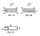
- FIGs. 1A and 1B an addressing scheme for controlling particle-based displays is shown in which electrodes are disposed on only one side of a display, allowing the display to be rear-addressed. Utilizing only one side of the display for electrodes simplifies fabrication of displays. For example, if the electrodes are disposed on only the rear side of a display, both of the electrodes can be fabricated using opaque materials, which may be colored, because the electrodes do not need to be transparent.
- FIG. 1 A depicts a single capsule 20 of an encapsulated display media.
- the embodiment depicted in FIG. 1A includes a capsule 20 containing at least one particle 50 dispersed in a suspending fluid 25.
- the capsule 20 is addressed by a first electrode 30 and a second electrode 40.
- the first electrode 30 is smaller than the second electrode 40.
- the first electrode 30 and the second electrode 40 may be set to voltage potentials which affect the position of the particles 50 in the capsule 20.
- the particles 50 represent 0.1 % to 20% of the volume enclosed by the capsule 20. In some embodiments the particles 50 represent 2.5% to 17.5% of the volume enclosed by capsule 20. In preferred embodiments, the particles 50 represent 5% to 15% of the volume enclosed by the capsule 20. In more preferred embodiments the particles 50 represent 9% to 11% of the volume defined by the capsule 20. In general, the volume percentage of the capsule 20 that the particles 50 represent should be selected so that the particles 50 expose most of the second, larger electrode 40 when positioned over the first, smaller electrode 30. As described in detail below, the particles 50 may be colored any one of a number of colors. The particles 50 may be either positively charged or negatively charged.
- the particles 50 are dispersed in a dispersing fluid 25.
- the dispersing fluid 25 should have a low dielectric constant.
- the fluid 25 may be clear, or substantially clear, so that the fluid 25 does not inhibit viewing the particles 50 and the electrodes 30, 40 from position 10.
- the fluid 25 is dyed.
- the dispersing fluid 25 has a specific gravity substantially matched to the density of the particles 50.
- the electrodes 30, 40 should be sized and positioned appropriately so that together they address the entire capsule 20. There may be exactly one pair of electrodes 30, 40 per capsule 20, multiple pairs of electrodes 30, 40 per capsule 20, or a single pair of electrodes 30, 40 may span multiple capsules 20. In the embodiment shown in FIGs. 1A and 1B , the capsule 20 has a flattened, rectangular shape. In these embodiments, the electrodes 30, 40 should address most, or all, of the flattened surface area adjacent the electrodes 30, 40.
- the smaller electrode 30 is at most one-half the size of the larger electrode 40. In preferred embodiments the smaller electrode is one-quarter the size of the larger electrode 40; in more preferred embodiments the smaller electrode 30 is one-eighth the size of the larger electrode 40.
- the smaller electrode 30 is one-sixteenth the size of the larger electrode 40. It should be noted that reference to "smaller” in connection with the electrode 30 means that the electrode 30 addresses a smaller amount of the surface area of the capsule 20, not necessarily that the electrode 30 is physically smaller than the larger electrode 40. For example, multiple capsules 20 may be positioned such that less of each capsule 20 is addressed by the "smaller" electrode 30, even though both electrodes 30, 40 are equal in size. It should also be noted that, as shown in FIG. 1C , electrode 30 may address only a small corner of a rectangular capsule 20 (shown in phantom view in FIG. 1 C) , requiring the larger electrode 40 to surround the smaller electrode 30 on two sides in order to properly address the capsule 20. Further, electrodes may be of any shape, such as concentric rings or rectangles. Selection of the percentage volume of the particles 50 and the electrodes 30, 40 in this manner allow the encapsulated display media to be addressed as described below.
- Electrodes generally may be fabricated from any material capable of conducting electricity so that electrode 30, 40 may apply an electric field to the capsule 20.
- conductive material may be printed by using conductive ink.
- Conductive inks are well known and may be prepared by including in the ink fluid a conductive material such as powdered metal or powdered graphite.
- the rear-addressed embodiments depicted in FIGs. 1A and 1B allow the electrodes 30, 40 to be fabricated from opaque materials such as solder paste, copper, copper-clad polyimide, graphite inks, silver inks and other metal-containing conductive inks.
- electrodes may be fabricated using transparent materials such as indium tin oxide and conductive polymers such as polyaniline or polythiopenes. Electrodes 30, 40 may be provided with contrasting optical properties. In some embodiments, one of the electrodes has an optical property complementary to optical properties of the particles 50. Alternatively, since the electrodes need not be transparent, an electrode can be constructed so as to display a selected color. Since electric current is not always required to be conducted from an electrode to a display element, but is only required to flow within the electrode to set up an electric field, one is in general able to overcoat the electrode with a colored ink so as to impart a desired color to an electrode, without detrimental effect on the operation of an electrode.
- the capsule 20 contains positively charged black particles 50, and a substantially clear suspending fluid 25.
- the first, smaller electrode 30 is colored black, and is smaller than the second electrode 40, which is colored white or is highly reflective.
- the positively-charged particles 50 migrate to the smaller, black electrode 30.
- the effect to a viewer of the capsule 20 located at position 10 is a mixture of the larger, white electrode 40 and the smaller, black electrode 30, creating an effect which is largely white. Referring to FIG.
- the capsule 20 may be addressed to display either a white visual state or a black visual state.
- varying the color of the smaller electrode 30 and the particles 50 allows fabrication of a rear-addressed, two-color display having black as one of the colors.
- varying the color of the smaller electrode 30 and the particles 50 allow a rear-addressed two-color system to be fabricated using white as one of the colors.
- the particles 50 and the smaller electrode 30 can be different colors.
- a two-color display may be fabricated having a second color that is different from the color of the smaller electrode 30 and the particles 50.
- a rear-addressed, orange-white display may be fabricated by providing blue particles 50, a red, smaller electrode 30, and a white (or highly reflective) larger electrode 40.
- the optical properties of the electrodes 30, 40 and the particles 50 can be independently selected to provide desired display characteristics.
- the optical properties of the dispersing fluid 25 may also be varied, e.g. the fluid 25 may be dyed.
- this technique may be used to provide a full color display.
- FIGs. 1D and 1E an embodiment is depicted that comprises three display elements. It should be understood that although FIGs. 1D and 1E depict rectangular elements having equally-sized display elements, an element may have any shape and a display may be comprised of display elements that are unequal in size or shape, or alternatively the display may be comprised of display elements that are unequal in number by color or optical property.
- the display elements may each be formed as a single large capsule, or each may be distributed across any number of small capsules or cells. For the purposes of illustration, the simpler case of a single large capsule for each display element is shown. In both cases we refer to the regions 20, 20', 20", as capsules.
- a first capsule 20 contains positively charged black particles 50 and a substantially clear suspending fluid 25.
- a first, smaller electrode 30 is colored black, and is smaller than the second electrode 40, which is colored red.
- the positively-charged particles 50 migrate to the smaller, black electrode 30.
- the effect to a viewer of the capsule 20 located at position 10 is a mixture of the larger, red electrode 40 and the smaller, black electrode 30, creating an effect which is largely red.
- the first capsule 20 may be addressed to display either a red visual state or a black visual state.
- a second capsule 20' contains positively charged black particles 50' and a substantially clear suspending fluid 25'.
- a first, smaller electrode 30' is colored black, and is smaller than the second electrode 40', which is colored green.
- a third capsule 20" contains positively charged black particles 50" and a substantially clear suspending fluid 25".
- a first, smaller electrode 30" is colored black, and is smaller than the second electrode 40", which is colored blue.
- the positively-charged particles 50" migrate to the smaller, black electrode 30".
- the effect to a viewer of the capsule 20" located at position 10" is a mixture of the larger, blue electrode 40" and the smaller, black electrode 30", creating an effect which is largely blue.
- the first, second and third capsules can have larger electrodes 40, 40', 40" which are respectively colored cyan, yellow, and magenta. Operation of the alternative cyan, yellow, and magenta embodiment is analogous to that of the red, green, and blue embodiment, with the feature that the color to be displayed is selected by a subtractive process.
- the larger electrode 40 may be transparent or reflective instead of white.
- the particles 50 when the particles 50 are moved to the smaller electrode 30, light reflects off the reflective surface of the larger electrode 40 and the capsule 20 appears light in color, e.g. white.
- the reflecting surface is obscured and the capsule 20 appears dark because light is absorbed by the particles 50 before reaching the reflecting surface.
- proper switching of the particles may be accomplished with a combination of alternating-current (AC) and direct-current (DC) electric fields.
- AC alternating-current
- DC direct-current
- the rear-addressed display previously discussed can be configured to transition between largely transmissive and largely opaque modes of operation (referred to hereafter as "shutter mode").
- the capsule 20 contains at least one positively-charged particle 50 dispersed in a substantially clear dispersing fluid 25.
- the larger electrode 40 is transparent and the smaller electrode 30 is opaque.
- the smaller, opaque electrode 30 is placed at a negative voltage potential relative to the larger, transmissive electrode 40, the particles 50 migrate to the smaller, opaque electrode 30.
- the effect to a viewer of the capsule 20 located at position 10 is a mixture of the larger, transparent electrode 40 and the smaller, opaque electrode 30, creating an effect which is largely transparent. Referring to FIG.
- FIGs. 1A and 1B when the smaller, opaque electrode 30 is placed at a positive voltage potential relative to the larger, transparent electrode 40, particles 50 migrate to the second electrode 40 and the viewer is presented a mixture of the opaque particles 50 covering the larger, transparent electrode 40 and the smaller, opaque electrode 30, creating an effect which is largely opaque.
- a display formed using the capsules depicted in FIGs. 1A and 1B may be switched between transmissive and opaque modes.
- the electrodes may be disposed on the viewing side of the capsule 20.
- Such a display can be used to construct a window that can be rendered opaque or a wide range of colors by using a tinted electrode.
- FIGs. 1A-1D depict a pair of electrodes associated with each capsule 20, it should be understood that each pair of electrodes may be associated with more than one capsule 20.
- a capsule 20 contains at least one dark or black particle 50 dispersed in a substantially clear dispersing fluid 25.
- a smaller, opaque electrode 30 and a larger, transparent electrode 40 apply both direct-current (DC) electric fields and alternating-current (AC) fields to the capsule 20.
- a DC field can be applied to the capsule 20 to cause the particles 50 to migrate towards the smaller electrode 30. For example, if the particles 50 are positively charged, the smaller electrode is placed a voltage that is more negative than the larger electrode 40.
- FIGs. 3A-3D depict only one capsule per electrode pair, multiple capsules may be addressed using the same electrode pair.
- the smaller electrode 30 is at most one-half the size of the larger electrode 40. In preferred embodiments the smaller electrode is one-quarter the size of the larger electrode 40; in more preferred embodiments the smaller electrode 30 is one-eighth the size of the larger electrode 40. In even more preferred embodiments, the smaller electrode 30 is one-sixteenth the size of the larger electrode 40.
- Causing the particles 50 to migrate to the smaller electrode 30, as depicted in FIG. 3A allows incident light to pass through the larger, transparent electrode 40 and be reflected by a reflecting surface 60.
- the reflecting surface 60 is replaced by a translucent layer, a transparent layer, or a layer is not provided at all, and incident light is allowed to pass through the capsule 20, i.e. the capsule 20 is transmissive.
- the translucent layer or the transparent layer comprises a color, such as a color filter
- the light that is transmitted will be those wavelengths that the filter passes, and the reflected light will consist of those wavelengths that the filter reflects, while the wavelengths that the filter absorbs will be lost.
- the visual appearance of a shutter mode display may thus depend on whether the display is in a transmissive or reflective condition, on the characteristics of the filter, and on the position of the viewer.
- the particles 50 are dispersed throughout the capsule 20 by applying an AC field to the capsule 20 via the electrodes 30, 40.
- the particles 50, dispersed into the capsule 20 by the AC field block incident light from passing through the capsule 20, causing it to appear dark at the viewpoint 10.
- the embodiment depicted in FIGs. 3A-3B may be used in shutter mode by not providing the reflecting surface 60 and instead providing a translucent layer, a transparent layer, a color filter layer, or no layer at all.
- shutter mode application of an AC electric field causes the capsule 20 to appear opaque.
- the transparency of a shutter mode display formed by the apparatus depicted in FIGs. 3A-3D may be controlled by the number of capsules addressed using DC fields and AC fields. For example, a display in which every other capsule 20 is addressed using an AC field would appear about half as transmissive as when the particles are all addressed by the AC field.
- FIGs. 3C and 3D depict an embodiment of the electrode structure described above in which electrodes 30, 40 are on "top" of the capsule 20, that is, the electrodes 30, 40 are between the viewpoint 10 and the capsule 20.
- both electrodes 30, 40 should be transparent.
- Transparent conducting layers can be fabricated using conductive polymers, such as polyaniline, polythiophenes, indium tin oxide, or polymers containing conducting particles lass than 100 nanometers in diameter such as copper iodide, ionic polymers, or slat-doped polymers. These materials may be made soluble so that electrodes can be fabricated using coating techniques such as spin coating, spray coating, meniscus coating, printing techniques, forward and reverse roll coating and the like.
- light passes through the electrodes 30, 40 and is either absorbed by the particles 50, reflected by reflecting layer 60 (when provided), transmitted throughout the capsule 20 (when reflecting layer 60 is not provided), or partially transmitted and/or reflected if a color filter is present in place of retroreflecting layer 60.
- each display element capsule 22, 22' and 22" each contain at least one white particle 50 dispersed in a substantially clear dispersing fluid 25.
- each display element capsule 22, 22' and 22" has a transparent electrode 42, 42', and 42" disposed above it and a colored filter 60, 60' and 60" disposed below it.
- a common reflective surface 70 may be shared behind the color filter layer.
- the display includes an emissive light source 70 Smaller, opaque electrodes 30, 30' and 30" and larger, transparent electrodes 40, 40' and 40" may apply direct-current (DC) electric fields and alternating-current (AC) fields to the capsules 20, 20' and 20".
- DC direct-current
- AC alternating-current
- a DC field can be applied to the capsules 20, 20' and 20" to cause the particles 50, 50' 50" to migrate towards the smaller electrodes 30, 30' and 30". For example, if the particles 50, 50' and 50" are positively charged, the smaller electrodes 30, 30' and 30" are placed a voltage that is more negative than the larger electrodes 40, 40' and 40".
- the smaller electrode 30 is at most one-half the size of the larger electrode 40. In preferred embodiments the smaller electrode 30 is one-quarter the size of the larger electrode 40; in more preferred embodiments the smaller electrode 30 is one-eighth the size of the larger electrode 40. In even more preferred embodiments, the smaller electrode 30 is one-sixteenth the size of the larger electrode 40.
- the filter layer 60 may be a translucent layer, a transparent layer, a color filter layer, or a layer is not provided at all, and further substrate 70 may be reflective, emissive, translucent or not provided at all. If the layer 60 comprises a color, such as a color filter, the light which is transmitted will be those wavelengths that the filter passes, and the reflected light will consist of those wavelengths that the filter reflects, while the wavelengths that the filter absorbs will be lost. The visual appearance of a the display element in 3E may thus depend on whether the display is in a transmissive or reflective condition, on the characteristics of the filter, and on the position of the viewer. In an alternative embodiment layer 60 may be provided on top of the capsule adjacent to electrode 42.
- Clear electrode 42 allows light to pass into capsule 22 and to strike either white particles W, red particles R, or a colored substrate 60.
- the substrate 60 can be a combination of color filter and non-colored substrate or it can be provided as a unitary colored substrate.
- Capsule 22 also includes a suspending fluid that can be dye-colored (possibly eliminating the need for a separate color filter 60) or substantially clear.
- Electrodes 45 and 35 are transparent and may be equally sized or sized in any suitable manner taking into account the relative particles sizes and mobilities of particles W and R. A gap exists between 45 and 35. Assume that particles W are negatively charged and particles R are positively charged. In FIG.
- top electrode 42 is set at a positive voltage potential relative to bottom electrodes 35 and 45, moving particles W to the top and particles R to the bottom and thus white is displayed.
- red is displayed in both FIGS. 3F and 3G.
- the particles obscure substrate 60.
- electrode 45 is at a negative voltage potential relative to electrode 35, while electrode 42 is at a voltage potential between the potentials of 45 and 35, such as zero.
- electrode 42 switches between the potentials of 45 and 35 so that over time the effective voltage of 42 is again between the potentials of 45 and 35.
- the particles R move toward electrode 45 and the particles W move toward electrode 35 and both particles R and W move away from the gap in the center of the capsule 22.
- the color combinations can differ.
- the specific colors of the filters and particles need not differ.
- This system called “dual particle curtain mode,” can image three arbitrary colors. In a preferred embodiment the colors are as described wherein one color is white and the other two colors are complements. In this manner, referring again to FIG. 3H , if a small portion of red is visible it absorbs part of the light reflected from the cyan substrate and the net result is black, which may be offset by a small portion of visible white. Thus, the element in FIG. 3H may appear to be cyan even if some red and white is visible. As mentioned above, the edges of the element may be masked to hide particles R and W when in the mode shown in FIG. 3H .
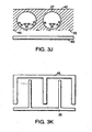
- FIG. 3I a full-color element is shown comprising three display elements, each operating in the manner taught by FIGS. 3F-3H wherein the colored particles are positively charged, and the white particles are negatively charged.
- the system may still function with top electrode 42 extended as a common top electrode as shown in FIG. 3I .
- electrodes 42, 45, 35, 45', 35', 45", 35" may be set to voltage potentials -30V, 60V, 60V, -60V, +60V, -60V, +60V respectively.
- Electrodes 45 and 35 are transparent and may be equally sized or sized in any suitable manner taking into account the relative particle sizes and mobilities of particles W and R. A gap exists between 45 and 35.
- FIG. 3K illustrates an embodiment of a suitable electrode pattern in which 45 and 35 are interdigitated.
- capsule 22 includes a suspending fluid 62 that is dyed cyan.
- suspending fluid 62 is substantially clear and a third species of cyan particles C is included in capsules 22. The cyan particles have a relatively neutral charge.
- electrodes 45 and 35 are set at appropriate voltages particles R and W move down to electrodes 45 and 35 respectively, revealing the cyan particles.
- FIGS. 3A-3M may be used with electrophoretic display media and encapsulated electrophoretic display media.
- the particles 50 exhibit bistability, that is, they are substantially motionless in the absence of a electric field.
- a preferred substrate for this use is an electroluminiscent (EL) backlight.
- EL electroluminiscent
- Such a backlight can be reflective when inactive, often with a whitish-green color, yet emit lights in various wavelengths when active.
- whitish EL substrates in place of static white reflective substrates, it is possible to construct a full-color reflective display that can also switch its mode of operation to display a range of colors in an emissive state, permitting operation in low ambient light conditions.
- FIGs. 4A and 4B depict an embodiment of a rear-addressing electrode structure that creates a reflective color display in a manner similar to halftoning or pointillism.
- the capsule 20 contains white particles 55 dispersed in a clear suspending fluid 25.
- Electrodes 42, 44, 46, 48 are colored cyan, magenta, yellow, and white respectively.
- FIG 4A when the colored electrodes 42, 44, 46 are placed at a positive potential relative to the white electrode 48, negatively-charged particles 55 migrate to these three electrodes, causing the capsule 20 to present to the viewpoint 10 a mix of the white particles 55 and the white electrode 48, creating an effect which is largely white.
- FIG. 4A when the colored electrodes 42, 44, 46 are placed at a positive potential relative to the white electrode 48, negatively-charged particles 55 migrate to these three electrodes, causing the capsule 20 to present to the viewpoint 10 a mix of the white particles 55 and the white electrode 48, creating an effect which is largely white.
- any color can be produced that is possible with a subtractive color process.
- the yellow electrode 46 and the magenta electrode 42 are set to a voltage potential that is more positive than the voltage potential applied by the cyan electrode 42 and the white electrode 48.
- the relative intensities of these colors can be controlled by the actual voltage potentials applied to the electrodes.
- AC current may be used appropriately to randomize the position of the particles as a step in this process.
- FIGS. 4A and 4B could be used in a similar manner with fewer electrodes and controlling fewer colors. For example, if electrode 42 were not present, the element could still display three colors. If electrodes 44 and 46 were colored red and cyan respectively, the capsule could display red, cyan and white. This construction could be used then employed as a display element, to be matched with similar display elements displaying other trios of colors thus achieving a full-color display as described above.
- the addressing structures described in FIGS. 1-4B typically comprise a top electrode controlled by display driver circuitry. It may be seen that if the top electrode is absent, the display may be imaged by an externally applied voltage source, such as a passing stylus or electrostatic print head.
- an externally applied voltage source such as a passing stylus or electrostatic print head.
- color electrophoretic displays require careful registration of display elements to the electrodes used to address those display elements.
- FIG. 5 steps that may be taken to efficiently and cheaply manufacture a display while avoiding the registration problems of prior art display are shown.
- a substrate is provided that has at least two electrodes (step 502).
- the number of electrodes provided will vary depending on the number of regions to be individually addressed. For example, in a traditional RGB display, three electrodes or sets of electrodes may be provided in order to address red capsules, green capsules, and blue capsules.
- the electrodes may have a predetermined pattern of interest.
- a display may include both electronic ink and traditional, printed inks. In such a display, the electrodes may be patterned to address only those portions of the display meant to bear electronic ink.
- the substrate is provided and the electrodes are printed on the substrate using any one of a number of printing techniques.
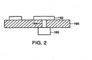
- FIG. 2 the structure of a printed electrode is shown.
- a conductive material 162 can be printed onto an insulative substrate 160.
- the substrate 160 defines one or more vias 164 that allow the printed conductive material 162 to be driven by addressing logic 166.
- the addressing logic 166 may also be printed.
- a first plurality of electrophoretic display elements is selectively printed on the substrate in substantial registration with at least one of the electrodes disposed on the substrate (step 504).
- the electrophoretic display elements generally are capsules containing one or more species of particles in a dispersing fluid as described above in connection with FIGs. 1-4B .
- the display elements which may form the contrast phase of an electronic ink, may be printed onto the substrate using any of the printing techniques described above. In certain embodiments, the printing technique itself provides the accuracy necessary to register the display elements to the appropriate electrode.
- an ink-jet printing process could be used to print red capsules in substantial registration with a "red” electrode, green capsules in substantial registration with a “green” electrode, and blue capsules in substantial registration with a “blue” electrode.
- the capsules can be printed sequentially or an ink-jet head may be used that allows red, green, and blue capsules to be simultaneously printed in a selective fashion.
- the display elements may be coated onto the substrate using an intermediate having a substantially cylindrical surface or a substantially flat surface, such as a lithographic belt.
- the intermediate is a roller, belt, blotter, brush, or sponge.
- the display elements may be held to the intermediate by electrostatic forces, surface tension, chemical bonding forces, or an applied electric field.
- the properties of the binder phase An be adjusted to match the desired printing process. For example, an ink to be used in inkjet printing may be adjusted to have a low viscosity. An ink suitable for lithographic printing may be adjusted to have a suitable contact angle.
- the display elements can be dispersed in a suitable carrier fluid such as water or an organic solvent that is dried after coating.
- the carrier fluid can also contain agents to modify surface tension, contact angle, viscosity, or electrical conductivity.
- the binder phase may contain monomers, oligomers, polymers, or polymerization inhibitors. These components can be used to form physically robust display element layers.
- the display elements could be dispersed in a low viscosity water solution containing a polymer. This solution could be inkjet printed in registration with the appropriate electrode pattern.
- the display element can be dispersed in an ultraviolet-curable resin used in lithographic printing processes, deposited on the appropriate electrodes by a lithographic process, and cured to form the display element layer. In all cases, the display elements are printed in substantial registration with the appropriate electrodes.
- the electronic ink is coated onto the substrate using an appropriate coating method such as knife-over-roll coating, silk-screen printing processes, brushing or other non-patterned coating techniques.
- an electric signal is applied to the electrode to which the display elements should be registered. Application of an electric signal attracts the display elements proximate the electrode.
- the applied signal overcomes the forces holding the display elements to the carrier and transfers the elements to the substrate adjacent the electrode.
- the display elements can be dispersed in a low viscosity liquid, such as low molecular weight hydrocarbons like methylethylketone or cyclohexane, or alcohols such as ethanol or propanol.
- the display elements are then treated to produce a controlled surface charge by, for example, adjusting the pH of the dispersing liquid or adding surface active agents such as soaps, detergents, or other dispersants. Because the charge of the display elements is controlled, an electric charge can be use to transfer the display elements to the appropriate electrode.
- display elements may then be removed from the substrate, e.g. by washing the substrate, to leave only the display elements that are proximate to the electrode.
- a second plurality of electrophoretic display elements are selectively deposited on the substrate in substantial registration with another electrode (step 506) using techniques similar to those just described.
- the technique used to selectively deposit the first plurality of display elements need not be the same technique as that used to selectively deposit the second plurality of display elements.
- This technique for printing displays can be used to build the rear electrode structure on a display or to construct two separate layers that are laminated together to form the display.
- an electronically active ink may be printed on an indium tin oxide electrode.
- a rear electrode structure as described above can be printed on a suitable substrate, such as plastic, polymer films, or glass.
- the electrode structure and the display element can be laminated to form a display.
Abstract
Description
- The present invention relates to methods of manufacturing color electrophoretic displays.
- Electrophoretic display media are generally characterized by the movement of particles through an applied electric field. These displays are highly reflective, can be made bistable, can be scaled to large areas, and consume very little power. These properties allow encapsulated electrophoretic display media to be used in many applications for which traditional electronic displays are not suitable. While bichromatic electrophoretic displays have been demonstrated in a limited range of colors (e.g. black/white or yellow/red), to date there has not been successful commercialization of a full-color electrophoretic display. One reason for this failure of commercialization is the lack of a method of manufacture that is efficient and inexpensive.
- One traditional technique for achieving a bright, full-color display which is known in the art of emissive displays is to create display elements that are red, green and blue. In this system, each element has two states: on, or the emission of color; and off. Since light blends from these elements, the overall display can take on a variety of colors and color combinations. In an emissive display, the visual result is the summation of the wavelengths emitted by the display elements at selected intensities, white is seen when red, green and blue are all active in balanced proportion. The brightness of the white image is controlled by the intensities of emission of light by the individual display elements. Black is seen when none are active or, equivalently, when all are emitting at zero intensity. As an additional example, a red visual display appears when the red display element is active while the green and blue are inactive, and thus only red light is emitted.
- This method can be applied to bichromatic reflective displays, typically using the cyan-magenta-yellow subtractive color system. In this system, the reflective display elements absorb characteristic portions of the optical spectrum, rather than generating characteristic portions of the spectrum as do the elements in an emissive display. White reflects everything, or equivalently absorbs nothing. A colored reflective material reflects light corresponding in wavelength to the color seen, and absorbs the remainder of the wavelengths in the visible spectrum. To achieve a black display, all three display elements are turned on, and they absorb complementary portions of the spectrum.
- However, such techniques require that the colored display elements be deposited onto a substrate in substantially equal proportions aligned with the proper addressing electrodes. Failure to achieve either substantially equal proportions of colored display elements or failure to achieve registration of the display elements with the addressing electrodes results in a color display that is unsatisfactory.
- Harbour et al., "Subdivided Electrophoretic Display", Xerox Disclosure Journal, , describes an electrophoretic display in which the imaging area is divided into cells, each of which represents one imaging element. The particles contained in each cell can settle only locally and redispersion with high-frequency, varying electrical fields is possible. An electrophoretic display imaging medium fills each of the cells and contains a dyed liquid and electrophoretic particles. The cells can be prepared with a photoresist material.
- Minnema et al.., "Pattern Generation in Polyimide Coatings and its Application in an Electrophoretic Image Display", Polymer Engineering and Science, Volume 28, Number 12 (30 June 1988), pages 815-822, describes direct photo-patterning of polyimide films based upon modification of the polyamic acid precursor. These modified precursors were processed like conventional negative photoresists, and are stated to be well suited for making the potential well structure of a microcell electrophoretic image display.
- Comiskey et al., "7.4L: Late-News Paper: Electrophoretic Ink: A Printable Display Material", 1997 SID Digest, pages 75-76, describes a method of manufacturing an electrophoretic display device by coating an electrophoretic electronically addressable ink using conventional printing techniques, for example, screen printing, on to an arbitrary surface. The ink is based on microcapsules containing either a dyed dielectric fluid and colored microparticles or an electrophoretic suspension based on two differently colored species of microparticles.
-
Japanese Published Patent Application No. 01-086116, published 30 March 1989 -
WO 98/19208 -
WO 99/53373 - This invention provides a method of manufacturing an electrophoretic display, the method comprising:
- (a) providing a substrate having an electrode disposed thereon; and
- (b) depositing on the substrate a plurality of electrophoretic display elements, each display element comprising a capsule containing a plurality of particles responsive to an applied electrical field and having a first optical property.
- This method is characterized by:
- (c) depositing the display elements in admixture with a curable material;
- (d) curing the curable material proximate the electrode, thereby fixing display elements proximate the electrode; and
- (e) removing from the substrate display elements not proximate the electrode.
- This invention teaches practical ways to efficiently and cheaply manufacture full-color, encapsulated electrophoretic displays. In one embodiment the display media can be printed and, therefore the display itself can be made inexpensively.
- An encapsulated electrophoretic display can be constructed so that the optical state of the display is stable for some length of time. When the display has two states which are stable in this manner, the display is said to be bistable. If more than two states of the display are stable, then the display can be said to be multistable. For the purpose of this invention, the terms bistable and multistable, or generally, stable, will be used to indicate a display in which any optical state remains fixed once the addressing voltage is removed. The definition of a stable state depends on the application for the display. A slowly-decaying optical state can be effectively stable if the optical state is substantially unchanged over the required viewing time. For example, in a display which is updated every few minutes, a display image which is stable for hours or days is effectively bistable or multistable, as the case may be, for that application. In this invention, the terms bistable and multistable also indicate a display with an optical state sufficiently long-lived as to be effectively stable for the application in mind. Alternatively, it is possible to construct encapsulated electrophoretic displays in which the image decays quickly once the addressing voltage to the display is removed (i.e., the display is not bistable or multistable). As will be described, in some applications it is advantageous to use an encapsulated electrophoretic display which is not bistable or multistable. Whether or not an encapsulated electrophoretic display is stable, and its degree of stability, can be controlled through appropriate chemical modification of the electrophoretic particles, the suspending fluid, the capsule, binder materials, or addressing methods.
- An encapsulated electrophoretic display may take many forms. The display may comprise capsules dispersed in a binder. The capsules may be of any size or shape. The capsules may, for example, be spherical and may have diameters in the millimeter range or the micron range, but is preferably from ten to a few hundred microns. The capsules may be formed by an encapsulation technique, as described below. Particles may be encapsulated in the capsules. The particles may be two or more different types of particles. The particles may be colored, luminescent, light-absorbing or transparent, for example. The particles may include neat pigments, dyed (laked) pigments or pigment/polymer composites, for example. The display may further comprise a suspending fluid in which the particles are dispersed.
- The successful construction of an encapsulated electrophoretic display requires the proper interaction of several different types of materials and processes, such as a polymeric binder and, optionally, a capsule membrane. These materials must be chemically compatible with the electrophoretic particles and fluid, as well as with each other. The capsule materials may engage in useful surface interactions with the electrophoretic particles, or may act as a chemical or physical boundary between the fluid and the binder. Various materials and combinations of materials useful in constructing encapsulated electrophoretic displays are described in co-pending application Serial No.
09/140,861 - In some cases, the encapsulation step of the process is not necessary, and the electrophoretic fluid may be directly dispersed or emulsified into the binder (or a precursor to the binder materials) and an effective "polymer-dispersed electrophoretic display" constructed. In such displays, voids created in the binder may be referred to as capsules or microcapsules even though no capsule membrane is present. The binder dispersed electrophoretic display may be of the emulsion or phase separation type.
- Throughout the Specification, reference will be made to printing or printed. As used throughout the specification, printing is intended to include all forms of printing and coating, including: premetered coatings such as patch die coating, slot or extrusion coating, slide or cascade coating, and curtain coating; roll coating such as knife over roll coating, forward and reverse roll coating; gravure coating; dip coating; spray coating; meniscus coating; spin coating; brush coating; air knife coating; silk screen printing processes; electrostatic printing processes; thermal printing processes; lithographic printing processes; ink-jet printing processes and other similar techniques. A "printed element" refers to an element formed using any one of the above techniques.
- As noted above, electrophoretic display elements can be encapsulated. Throughout the Specification, reference will be made to "capsules," "elements," and "display elements." A capsule or display element may itself comprise one or more capsules or other structures.
- The advantages of the invention described above, together with further advantages, may be better understood by referring to the following description taken in conjunction with the accompanying drawings. In the drawings, like reference characters generally refer to the same parts throughout the different views. Also, the drawings are not necessarily to scale, emphasis instead generally being placed upon illustrating the principles of the invention.
-
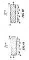
FIG. 1A is a diagrammatic side view of an embodiment of a rear-addressing electrode structure for a particle-based display in which a smaller electrode has been placed at a voltage relative to the large electrode causing the particles to migrate to the smaller electrode. -
FIG. 1B is a diagrammatic side view of an embodiment of a rear-addressing electrode structure for a particle-based display in which the larger electrode has been placed at a voltage relative to the smaller electrode causing the particles to migrate to the larger electrode. -
FIG. 1C is a diagrammatic top-down view of one embodiment of a rear-addressing electrode structure. -
FIG. 1D is a diagrammatic side view of one embodiment ofa display having three display elements, each display element being produced by a printing process. -
FIG. 1E is a diagrammatic plan view of one embodiment of a display having three display elements, each display element being produced by a printing process. -
FIG. 2 is a cross-sectional view of a rear electrode addressing structure that is formed by printing. -
FIG. 3A is a schematic flow diagram of selected steps in a method of manufacturing a display that employs a process in which electrodes are first printed on a substrate, followed by the printing of display elements upon the electrodes. -
FIG. 3B is a schematic flow diagram of selected steps in a method of manufacturing a display that employs a process in which display elements are first printed on a substrate, followed by the printing of electrodes upon the display elements. -
FIG. 3C is a schematic flow diagram of selected steps in a method of manufacturing a display that employs a process in which electrodes are printed on a first substrate, display elements are printed on a second substrate, and the two structures are combined to form a display. -
FIG. 3D is a diagrammatic side view of an embodiment of an addressing structure having transparent electrodes, in which an alternating-current electric field has been applied to the capsule causing the particles to disperse into the capsule. -
FIG. 3E is a diagrammatic side view of an embodiment of an addressing structure for a display element having three sub-pixels. -
FIG. 3F is a diagrammatic side view of an embodiment of a dual particle curtain mode addressing structure addressing a display element to appear white. -
FIG. 3G is a diagrammatic side view of an embodiment of a dual particle curtain mode addressing structure addressing a display element to appear red. -
FIG. 3H is a diagrammatic side view of an embodiment of a dual particle curtain mode addressing structure addressing a display element to absorb red light. -
FIG. 3I is a diagrammatic side view of an embodiment of a dual particle curtain mode addressing structure for a display element having three sub-pixels, in which the display is addressed to appear red. -
FIG. 3J is a diagrammatic side view of another embodiment of a dual particle curtain mode addressing structure for a display element. -
FIG. 3K is a diagrammatic plan view of an embodiment of an interdigitated electrode structure. -
FIG. 3L is a diagrammatic side view of another embodiment of a dual particle curtain mode display structure having a dyed fluid and two species of particles, addressed to absorb red. -
FIG. 3M is a diagrammatic side view of another embodiment of a dual particle curtain mode display structure having clear fluid and three species of particles, addressed to absorb red. -
FIGs. 4A and 4B depict a rear-addressing electrode structure that creates a reflective color display in a manner similar to half-toning or pointillism. -
FIG. 5 is a flowchart showing the steps to be taken to fabricate a display using a method of the present invention. - Electronic ink is an optoelectronically active material that comprises at least two phases: an electrophoretic contrast media phase and a coating/binding phase. The electrophoretic phase comprises, in some embodiments, a single species of electrophoretic particles dispersed in a clear or dyed medium, or more than one species of electrophoretic particles having distinct physical and electrical characteristics dispersed in a clear or dyed medium. In some embodiments the electrophoretic phase is encapsulated, that is, there is a capsule wall phase between the two phases. The coating/binding phase includes, in one embodiment, a polymer matrix that surrounds the electrophoretic phase. In this embodiment, the polymer in the polymeric binder is capable of being dried, crosslinked, or otherwise cured as in traditional inks, and therefore a printing process can be used to deposit the electronic ink onto a substrate.
- In one embodiment, the ink may comprise display elements capable of displaying different colors. In one particular embodiment, some display elements contain red particles, some display elements contain green particles, and some display elements contain blue particles, respectively. In another particular embodiment, some display elements contain cyan particles, some display elements contain magenta particles, and some display elements contain yellow particles, respectively. By addressing each display element to display some fraction of its colored particles, a display can be caused to give an appearance corresponding to a selected color at a selected brightness level.
- Electronic ink is capable of being printed by several different processes, depending on the mechanical properties of the specific ink employed. For example, the fragility or viscosity of a particular ink may result in a different process selection. A very viscous ink would not be well-suited to deposition by an inkjet printing process, while a fragile ink might not be used in a knife over roll coating process.
- The optical quality of an electronic ink is quite distinct from other electronic display materials. The most notable difference is that the electronic ink provides a high degree of both reflectance and contrast because it is pigment based (as are ordinary printing inks). The light scattered from the electronic ink comes from a very thin layer of pigment close to the viewing surface. In this respect it resembles an ordinary, printed image. Also, electronic ink is easily viewed from a wide range of viewing angles in the same manner as a printed page, and such ink approximates a Lambertian contrast curve more closely than any other electronic display material. Since electronic ink can be printed, it can be included on the same surface with any other printed material, including traditional inks. Electronic ink can be made optically stable in all display configurations, that is, the ink can be set to a persistent optical state. Fabrication of a display by printing an electronic ink is particularly useful in low power applications because of this stability.
- Electronic ink displays are novel in that they can be addressed by DC voltages and draw very little current. Therefore, elements forming electronic inks may be made of non-traditional materials and electronic inks may be manufactured by and used in non-traditional methods. As such, the conductive leads and electrodes used to deliver the voltage to electronic ink displays can be of relatively high resistivity. The ability to use resistive conductors substantially widens the number and type of materials that can be used as conductors in electronic ink displays. In particular, the use of costly vacuum-sputtered indium tin oxide (ITO) conductors, a standard material in liquid crystal devices, is not required. Aside from cost savings, the replacement of ITO with other materials can provide benefits in appearance, processing capabilities (printed conductors), flexibility, and durability. Additionally, the printed electrodes are in contact only with a solid binder, not with a fluid layer (like liquid crystals). This means that some conductive materials, which would otherwise dissolve or be degraded by contact with liquid crystals, can be used in an electronic ink application. These include opaque metallic inks for the rear electrode (e.g., silver and graphite inks), as well as conductive transparent inks for either substrate. These conductive coatings include semiconducting colloids, examples of which are indium tin oxide and antimony-doped tin oxide. Organic conductors (polymeric conductors and molecular organic conductors) also may be used. Polymers include, but are not limited to, polyaniline and derivatives, polythiophene and derivatives, poly3,4-ethylenedioxythiophene (PEDOT) and derivatives, polypyrrole and derivatives, and polyphenylenevinylene (PPV) and derivatives. Organic molecular conductors include, but are not limited to, derivatives of naphthalene, phthalocyanine, and pentacene. Polymer layers can be made thinner and more transparent than with traditional displays because conductivity requirements are not as stringent.
- As an example, there is a class of materials called electroconductive powders which are also useful as coatable transparent conductors in electronic ink displays. One example is Zelec ECP electroconductive powders from DuPont Chemical Co. of Wilmington, Delaware.
- It is possible to produce a wide gamut of colors from the superposition of suitable proportions of three properly chosen colors. In one embodiment, the colors red, green, and blue can be combined in various proportions to produce an image that is perceived as a selected color. Emissive or transmissive displays operate according to additive rules, where the perceived color is created by summing the emission wavelengths of a plurality of emitting or transmitting objects. For an emissive or transmissive display that includes three display elements, one of which can produce red light, one green light, and one blue light, respectively, one can generate a wide gamut of colors, as well as white and black. At one extreme, the combination of all three at full intensity is perceived as white, and at the other, the combination of all three at zero intensity is perceived as black. Specific combinations of controlled proportions of these three colors can be used to represent other colors.
- In a reflective display, the light that a viewer perceives is the portion of the spectrum that is not absorbed when the light to be reflected falls on the reflector surface. One may thus consider a reflecting system as a subtractive system, that is, that each reflective surface "subtracts" from the light that portion which the reflector absorbs. The color of a reflector represents the wavelengths of light the reflector absorbs. A yellow reflector absorbs substantially blue light. A magenta reflector absorbs substantially green light. A cyan reflector absorbs substantially red light. Thus, in an alternative embodiment employing reflectors, nearly the same results as an emissive system can be obtained by use of the three colors cyan, yellow, and magenta as the primary colors, from which all other colors, including black but not white, can be derived. To obtain white from such a display, one must further introduce a third state per display element, namely white.
- While the methods described discuss particles, any combination of dyes, liquids droplets and transparent regions that respond to electrophoretic effects could also be used. Particles of various optical effects may be combined in any suitable proportion. For example, certain colors may be over- or under-populated in the electrophoretic display, for example, by printing more display elements of one color than of another color, to account for the sensitivities of the human eye and to thereby achieve a more pleasing or uniform effect. Similarly, the sizes of the display elements may also be disproportionate to achieve various optical effects.
- Although these examples describe microencapsulated electrophoretic displays, the invention can be utilized across other reflective displays including liquid crystal, polymer-dispersed liquid crystal, rotating ball, suspended particle and any other reflective display capable of being printed. In short, many schemes are possible by which display elements in a direct color reflective display can be printed. Such printing schemes will vary by the nature of the display and any suitable means may be used.
- Referring now to
FIGs. 1A and 1B , an addressing scheme for controlling particle-based displays is shown in which electrodes are disposed on only one side of a display, allowing the display to be rear-addressed. Utilizing only one side of the display for electrodes simplifies fabrication of displays. For example, if the electrodes are disposed on only the rear side of a display, both of the electrodes can be fabricated using opaque materials, which may be colored, because the electrodes do not need to be transparent. -
FIG. 1 A depicts asingle capsule 20 of an encapsulated display media. In brief overview, the embodiment depicted inFIG. 1A includes acapsule 20 containing at least oneparticle 50 dispersed in a suspendingfluid 25. Thecapsule 20 is addressed by afirst electrode 30 and asecond electrode 40. Thefirst electrode 30 is smaller than thesecond electrode 40. Thefirst electrode 30 and thesecond electrode 40 may be set to voltage potentials which affect the position of theparticles 50 in thecapsule 20. - The
particles 50 represent 0.1 % to 20% of the volume enclosed by thecapsule 20. In some embodiments theparticles 50 represent 2.5% to 17.5% of the volume enclosed bycapsule 20. In preferred embodiments, theparticles 50 represent 5% to 15% of the volume enclosed by thecapsule 20. In more preferred embodiments theparticles 50 represent 9% to 11% of the volume defined by thecapsule 20. In general, the volume percentage of thecapsule 20 that theparticles 50 represent should be selected so that theparticles 50 expose most of the second,larger electrode 40 when positioned over the first,smaller electrode 30. As described in detail below, theparticles 50 may be colored any one of a number of colors. Theparticles 50 may be either positively charged or negatively charged. - The
particles 50 are dispersed in a dispersingfluid 25. The dispersingfluid 25 should have a low dielectric constant. The fluid 25 may be clear, or substantially clear, so that the fluid 25 does not inhibit viewing theparticles 50 and theelectrodes position 10. In other embodiments, the fluid 25 is dyed. In some embodiments the dispersingfluid 25 has a specific gravity substantially matched to the density of theparticles 50. These embodiments can provide a bistable display media, because theparticles 50 do not tend to move absent an electric field applied via theelectrodes - The
electrodes entire capsule 20. There may be exactly one pair ofelectrodes capsule 20, multiple pairs ofelectrodes capsule 20, or a single pair ofelectrodes multiple capsules 20. In the embodiment shown inFIGs. 1A and 1B , thecapsule 20 has a flattened, rectangular shape. In these embodiments, theelectrodes electrodes smaller electrode 30 is at most one-half the size of thelarger electrode 40. In preferred embodiments the smaller electrode is one-quarter the size of thelarger electrode 40; in more preferred embodiments thesmaller electrode 30 is one-eighth the size of thelarger electrode 40. In even more preferred embodiments, thesmaller electrode 30 is one-sixteenth the size of thelarger electrode 40. It should be noted that reference to "smaller" in connection with theelectrode 30 means that theelectrode 30 addresses a smaller amount of the surface area of thecapsule 20, not necessarily that theelectrode 30 is physically smaller than thelarger electrode 40. For example,multiple capsules 20 may be positioned such that less of eachcapsule 20 is addressed by the "smaller"electrode 30, even though bothelectrodes FIG. 1C ,electrode 30 may address only a small corner of a rectangular capsule 20 (shown in phantom view inFIG. 1 C) , requiring thelarger electrode 40 to surround thesmaller electrode 30 on two sides in order to properly address thecapsule 20. Further, electrodes may be of any shape, such as concentric rings or rectangles. Selection of the percentage volume of theparticles 50 and theelectrodes - Electrodes generally may be fabricated from any material capable of conducting electricity so that
electrode capsule 20. In the embodiments to be discussed here, conductive material may be printed by using conductive ink. Conductive inks are well known and may be prepared by including in the ink fluid a conductive material such as powdered metal or powdered graphite. As noted above, the rear-addressed embodiments depicted inFIGs. 1A and 1B allow theelectrodes Electrodes particles 50. Alternatively, since the electrodes need not be transparent, an electrode can be constructed so as to display a selected color. Since electric current is not always required to be conducted from an electrode to a display element, but is only required to flow within the electrode to set up an electric field, one is in general able to overcoat the electrode with a colored ink so as to impart a desired color to an electrode, without detrimental effect on the operation of an electrode. - The operation of the electrophoretic display element will be presented with regard to an embodiment that displays two states, for example, black and white. In this embodiment, the
capsule 20 contains positively chargedblack particles 50, and a substantially clear suspendingfluid 25. The first,smaller electrode 30 is colored black, and is smaller than thesecond electrode 40, which is colored white or is highly reflective. When the smaller,black electrode 30 is placed at a negative voltage potential relative to larger,white electrode 40, the positively-chargedparticles 50 migrate to the smaller,black electrode 30. The effect to a viewer of thecapsule 20 located atposition 10 is a mixture of the larger,white electrode 40 and the smaller,black electrode 30, creating an effect which is largely white. Referring toFIG. 1B , when the smaller,black electrode 30 is placed at a positive voltage potential relative to the larger,white electrode 40,particles 50 migrate to the larger,white electrode 40 and the viewer is presented a mixture of theblack particles 50 covering the larger,white electrode 40 and the smaller,black electrode 30, creating an effect which is largely black. In this manner thecapsule 20 may be addressed to display either a white visual state or a black visual state. - Other two-color schemes are easily provided by varying the color of the
smaller electrode 30 and theparticles 50 or by varying the color of thelarger electrode 40. For example, varying the color of thelarger electrode 40 allows fabrication of a rear-addressed, two-color display having black as one of the colors. Alternatively, varying the color of thesmaller electrode 30 and theparticles 50 allow a rear-addressed two-color system to be fabricated using white as one of the colors. Further, it is contemplated that theparticles 50 and thesmaller electrode 30 can be different colors. In these embodiments, a two-color display may be fabricated having a second color that is different from the color of thesmaller electrode 30 and theparticles 50. For example, a rear-addressed, orange-white display may be fabricated by providingblue particles 50, a red,smaller electrode 30, and a white (or highly reflective)larger electrode 40. In general, the optical properties of theelectrodes particles 50 can be independently selected to provide desired display characteristics. In some embodiments the optical properties of the dispersingfluid 25 may also be varied, e.g. the fluid 25 may be dyed. - In another embodiment, this technique may be used to provide a full color display. Referring now to
FIGs. 1D and 1E , an embodiment is depicted that comprises three display elements. It should be understood that althoughFIGs. 1D and 1E depict rectangular elements having equally-sized display elements, an element may have any shape and a display may be comprised of display elements that are unequal in size or shape, or alternatively the display may be comprised of display elements that are unequal in number by color or optical property. The display elements may each be formed as a single large capsule, or each may be distributed across any number of small capsules or cells. For the purposes of illustration, the simpler case of a single large capsule for each display element is shown. In both cases we refer to theregions first capsule 20 contains positively chargedblack particles 50 and a substantially clear suspendingfluid 25. A first,smaller electrode 30 is colored black, and is smaller than thesecond electrode 40, which is colored red. When the smaller,black electrode 30 is placed at a negative voltage potential relative to larger,red electrode 40, the positively-chargedparticles 50 migrate to the smaller,black electrode 30. The effect to a viewer of thecapsule 20 located atposition 10 is a mixture of the larger,red electrode 40 and the smaller,black electrode 30, creating an effect which is largely red. When the smaller,black electrode 30 is placed at a positive voltage potential relative to the larger,red electrode 40,particles 50 migrate to the larger,red electrode 40 and the viewer is presented a mixture of theblack particles 50 covering the larger,red electrode 40 and the smaller,black electrode 30, creating an effect which is largely black. In this manner thefirst capsule 20 may be addressed to display either a red visual state or a black visual state. One can equally have a second capsule 20' wherein the larger electrode 40' is green, and athird capsule 20" wherein thelarger electrode 40" is blue. A second capsule 20' contains positively charged black particles 50' and a substantially clear suspending fluid 25'. A first, smaller electrode 30' is colored black, and is smaller than the second electrode 40', which is colored green. When the smaller, black electrode 30' is placed at a negative voltage potential relative to larger, green electrode 40', the positively-charged particles 50' migrate to the smaller, black electrode 30'. The effect to a viewer of the capsule 20' located at position 10' is a mixture of the larger, green electrode 40' and the smaller, black electrode 30', creating an effect which is largely green. When the smaller, black electrode 30' is placed at a positive voltage potential relative to the larger, green electrode 40', particles 50' migrate to the larger, green electrode 40' and the viewer is presented a mixture of the black particles 50' covering the larger, green electrode 40' and the smaller, black electrode 30', creating an effect which is largely black. Similarly, athird capsule 20" contains positively chargedblack particles 50" and a substantially clear suspendingfluid 25". A first,smaller electrode 30" is colored black, and is smaller than thesecond electrode 40", which is colored blue. When the smaller,black electrode 30" is placed at a negative voltage potential relative to larger,blue electrode 40", the positively-chargedparticles 50" migrate to the smaller,black electrode 30". The effect to a viewer of thecapsule 20" located atposition 10" is a mixture of the larger,blue electrode 40" and the smaller,black electrode 30", creating an effect which is largely blue. When the smaller,black electrode 30" is placed at a positive voltage potential relative to the larger,blue electrode 40",particles 50" migrate to the larger,blue electrode 40" and the viewer is presented a mixture of theblack particles 50" covering the larger,blue electrode 40" and the smaller,black electrode 30", creating an effect which is largely black. Further, the relative intensities of these colors can be controlled by the actual voltage potentials applied to the electrodes. By choosing appropriate combinations of the three colors, one may create a visual display which appears as the effective combination of the selected colors as an additive process. As an alternative embodiment, the first, second and third capsules can havelarger electrodes - In other embodiments the
larger electrode 40 may be transparent or reflective instead of white. In these embodiments, when theparticles 50 are moved to thesmaller electrode 30, light reflects off the reflective surface of thelarger electrode 40 and thecapsule 20 appears light in color, e.g. white. When theparticles 50 are moved to thelarger electrode 40, the reflecting surface is obscured and thecapsule 20 appears dark because light is absorbed by theparticles 50 before reaching the reflecting surface. In other embodiments, proper switching of the particles may be accomplished with a combination of alternating-current (AC) and direct-current (DC) electric fields. - In still other embodiments, the rear-addressed display previously discussed can be configured to transition between largely transmissive and largely opaque modes of operation (referred to hereafter as "shutter mode"). Referring back to
FIGs. 1A and 1B , in these embodiments thecapsule 20 contains at least one positively-chargedparticle 50 dispersed in a substantially clear dispersingfluid 25. Thelarger electrode 40 is transparent and thesmaller electrode 30 is opaque. When the smaller,opaque electrode 30 is placed at a negative voltage potential relative to the larger,transmissive electrode 40, theparticles 50 migrate to the smaller,opaque electrode 30. The effect to a viewer of thecapsule 20 located atposition 10 is a mixture of the larger,transparent electrode 40 and the smaller,opaque electrode 30, creating an effect which is largely transparent. Referring toFIG. 1B , when the smaller,opaque electrode 30 is placed at a positive voltage potential relative to the larger,transparent electrode 40,particles 50 migrate to thesecond electrode 40 and the viewer is presented a mixture of theopaque particles 50 covering the larger,transparent electrode 40 and the smaller,opaque electrode 30, creating an effect which is largely opaque. In this manner, a display formed using the capsules depicted inFIGs. 1A and 1B may be switched between transmissive and opaque modes. In some embodiments the electrodes may be disposed on the viewing side of thecapsule 20. Such a display can be used to construct a window that can be rendered opaque or a wide range of colors by using a tinted electrode. AlthoughFIGs. 1A-1D depict a pair of electrodes associated with eachcapsule 20, it should be understood that each pair of electrodes may be associated with more than onecapsule 20. - A similar technique may be used in connection with the embodiment of
FIGs. 3A, 3B, 3C, and 3D . Referring toFIG. 3A , acapsule 20 contains at least one dark orblack particle 50 dispersed in a substantially clear dispersingfluid 25. A smaller,opaque electrode 30 and a larger,transparent electrode 40 apply both direct-current (DC) electric fields and alternating-current (AC) fields to thecapsule 20. A DC field can be applied to thecapsule 20 to cause theparticles 50 to migrate towards thesmaller electrode 30. For example, if theparticles 50 are positively charged, the smaller electrode is placed a voltage that is more negative than thelarger electrode 40. AlthoughFIGs. 3A-3D depict only one capsule per electrode pair, multiple capsules may be addressed using the same electrode pair. - The
smaller electrode 30 is at most one-half the size of thelarger electrode 40. In preferred embodiments the smaller electrode is one-quarter the size of thelarger electrode 40; in more preferred embodiments thesmaller electrode 30 is one-eighth the size of thelarger electrode 40. In even more preferred embodiments, thesmaller electrode 30 is one-sixteenth the size of thelarger electrode 40. - Causing the
particles 50 to migrate to thesmaller electrode 30, as depicted inFIG. 3A , allows incident light to pass through the larger,transparent electrode 40 and be reflected by a reflectingsurface 60. In shutter mode, the reflectingsurface 60 is replaced by a translucent layer, a transparent layer, or a layer is not provided at all, and incident light is allowed to pass through thecapsule 20, i.e. thecapsule 20 is transmissive. If the translucent layer or the transparent layer comprises a color, such as a color filter, the light that is transmitted will be those wavelengths that the filter passes, and the reflected light will consist of those wavelengths that the filter reflects, while the wavelengths that the filter absorbs will be lost. The visual appearance of a shutter mode display may thus depend on whether the display is in a transmissive or reflective condition, on the characteristics of the filter, and on the position of the viewer. - Referring now to
FIG. 3B , theparticles 50 are dispersed throughout thecapsule 20 by applying an AC field to thecapsule 20 via theelectrodes particles 50, dispersed into thecapsule 20 by the AC field, block incident light from passing through thecapsule 20, causing it to appear dark at theviewpoint 10. The embodiment depicted inFIGs. 3A-3B may be used in shutter mode by not providing the reflectingsurface 60 and instead providing a translucent layer, a transparent layer, a color filter layer, or no layer at all. In shutter mode, application of an AC electric field causes thecapsule 20 to appear opaque. The transparency of a shutter mode display formed by the apparatus depicted inFIGs. 3A-3D may be controlled by the number of capsules addressed using DC fields and AC fields. For example, a display in which everyother capsule 20 is addressed using an AC field would appear about half as transmissive as when the particles are all addressed by the AC field. -
FIGs. 3C and 3D depict an embodiment of the electrode structure described above in whichelectrodes capsule 20, that is, theelectrodes viewpoint 10 and thecapsule 20. In these embodiments, bothelectrodes electrodes particles 50, reflected by reflecting layer 60 (when provided), transmitted throughout the capsule 20 (when reflectinglayer 60 is not provided), or partially transmitted and/or reflected if a color filter is present in place ofretroreflecting layer 60. - Referring to
FIG. 3E , threedisplay element capsules white particle 50 dispersed in a substantially clear dispersingfluid 25. In one embodiment, eachdisplay element capsule transparent electrode colored filter reflective surface 70 may be shared behind the color filter layer. In an alternative embodiment, the display includes an emissivelight source 70
Smaller,opaque electrodes transparent electrodes capsules capsules particles 50, 50' 50" to migrate towards thesmaller electrodes particles smaller electrodes larger electrodes - The
smaller electrode 30 is at most one-half the size of thelarger electrode 40. In preferred embodiments thesmaller electrode 30 is one-quarter the size of thelarger electrode 40; in more preferred embodiments thesmaller electrode 30 is one-eighth the size of thelarger electrode 40. In even more preferred embodiments, thesmaller electrode 30 is one-sixteenth the size of thelarger electrode 40. - Causing the
particles 50 to migrate to thesmaller electrode 30, as depicted in the first two capsules ofFIG. 3E , allows incident light to pass through the larger,transparent electrode 40, throughfilter 60, reflect offsubstrate 70 and pass back through the device. If the first, second andthird filters particles 50 are white, this system can display full color in a standard two-color fashion. - The
filter layer 60 may be a translucent layer, a transparent layer, a color filter layer, or a layer is not provided at all, andfurther substrate 70 may be reflective, emissive, translucent or not provided at all. If thelayer 60 comprises a color, such as a color filter, the light which is transmitted will be those wavelengths that the filter passes, and the reflected light will consist of those wavelengths that the filter reflects, while the wavelengths that the filter absorbs will be lost. The visual appearance of a the display element in 3E may thus depend on whether the display is in a transmissive or reflective condition, on the characteristics of the filter, and on the position of the viewer. In analternative embodiment layer 60 may be provided on top of the capsule adjacent toelectrode 42. - Referring now to
FIGS. 3F-3K , one embodiment of a tri-color element is described.Clear electrode 42 allows light to pass intocapsule 22 and to strike either white particles W, red particles R, or acolored substrate 60. Thesubstrate 60 can be a combination of color filter and non-colored substrate or it can be provided as a unitary colored substrate.Capsule 22 also includes a suspending fluid that can be dye-colored (possibly eliminating the need for a separate color filter 60) or substantially clear.Electrodes FIG. 3F ,top electrode 42 is set at a positive voltage potential relative tobottom electrodes FIG. 3G by reversing the polarity of the electrodes, red is displayed. In bothFIGS. 3F and 3G the particlesobscure substrate 60. InFIG. 3H electrode 45 is at a negative voltage potential relative toelectrode 35, whileelectrode 42 is at a voltage potential between the potentials of 45 and 35, such as zero. Alternatively,electrode 42 switches between the potentials of 45 and 35 so that over time the effective voltage of 42 is again between the potentials of 45 and 35. In this state, the particles R move towardelectrode 45 and the particles W move towardelectrode 35 and both particles R and W move away from the gap in the center of thecapsule 22. This revealssubstrate 60, permitting a third color such as cyan to be imaged. In alternate embodiments the color combinations can differ. The specific colors of the filters and particles need not differ. This system, called "dual particle curtain mode," can image three arbitrary colors. In a preferred embodiment the colors are as described wherein one color is white and the other two colors are complements. In this manner, referring again toFIG. 3H , if a small portion of red is visible it absorbs part of the light reflected from the cyan substrate and the net result is black, which may be offset by a small portion of visible white. Thus, the element inFIG. 3H may appear to be cyan even if some red and white is visible. As mentioned above, the edges of the element may be masked to hide particles R and W when in the mode shown inFIG. 3H . - Referring now to
FIG. 3I , a full-color element is shown comprising three display elements, each operating in the manner taught byFIGS. 3F-3H wherein the colored particles are positively charged, and the white particles are negatively charged. The system may still function withtop electrode 42 extended as a common top electrode as shown inFIG. 3I . For example, to achieve the state shown,electrodes - Referring now to
FIGS. 3J-3K , an electrode scheme is shown whereby a cluster of microcapsules may be addressed for an entire display element in a manner similar to those described above.Clear electrode 42 allows light to pass intomicrocapsules 27 and to strike either white particles W, red particles R, orcolored substrate 60. As above,colored substrate 60 may be a combination of color filter andnon-colored substrate 60 orcolored substrate 60 may be provided as a unitary colored substrate.Capsules 27 include a suspending fluid that may be dye-colored (possibly eliminating the need for a separate color filter 60) or substantially clear.Electrodes FIGS. 3F-3K , although for any givenmicrocapsule 27 there may be multiple gaps.FIG. 3K illustrates an embodiment of a suitable electrode pattern in which 45 and 35 are interdigitated. - Referring now to 3L-3M, an alternate embodiment is shown. Again
clear electrode 42 allows light to pass intocapsule 22 and to strike white particles W or red particles R. In the embodiment shown inFIG. 3L ,capsule 22 includes a suspendingfluid 62 that is dyed cyan. Whenelectrodes electrodes fluid 62. Alternatively, as shown inFIG. 3M , suspendingfluid 62 is substantially clear and a third species of cyan particles C is included incapsules 22. The cyan particles have a relatively neutral charge. Whenelectrodes electrodes - The addressing structure depicted in
FIGS. 3A-3M may be used with electrophoretic display media and encapsulated electrophoretic display media.FIGS. 3A-3M depict embodiments in whichelectrode particles 50 exhibit bistability, that is, they are substantially motionless in the absence of a electric field. - While various of the substrates described above are reflective, an analogous technique may be employed wherein the substrates emit light, with the particles again acting in a "shutter mode" to reveal or obscure light. A preferred substrate for this use is an electroluminiscent (EL) backlight. Such a backlight can be reflective when inactive, often with a whitish-green color, yet emit lights in various wavelengths when active. By using whitish EL substrates in place of static white reflective substrates, it is possible to construct a full-color reflective display that can also switch its mode of operation to display a range of colors in an emissive state, permitting operation in low ambient light conditions.
-
FIGs. 4A and 4B depict an embodiment of a rear-addressing electrode structure that creates a reflective color display in a manner similar to halftoning or pointillism. Thecapsule 20 contains white particles 55 dispersed in a clear suspendingfluid 25.Electrodes 42, 44, 46, 48 are colored cyan, magenta, yellow, and white respectively. Referring toFIG 4A , when thecolored electrodes 42, 44, 46 are placed at a positive potential relative to the white electrode 48, negatively-charged particles 55 migrate to these three electrodes, causing thecapsule 20 to present to the viewpoint 10 a mix of the white particles 55 and the white electrode 48, creating an effect which is largely white. Referring toFIG. 4B , whenelectrodes 42, 44, 46 are placed at a negative potential relative to electrode 48, particles 55 migrate to the white electrode 48, and theeye 10 sees a mix of the white particles 55, thecyan electrode 42, the magenta electrode 44, and the yellow electrode 46, creating an effect which is largely black or gray. By addressing the electrodes, any color can be produced that is possible with a subtractive color process. For example, to cause thecapsule 20 to display a red color to theviewpoint 10, the yellow electrode 46 and themagenta electrode 42 are set to a voltage potential that is more positive than the voltage potential applied by thecyan electrode 42 and the white electrode 48. Further, the relative intensities of these colors can be controlled by the actual voltage potentials applied to the electrodes. Again, AC current may be used appropriately to randomize the position of the particles as a step in this process. - The technique used in
FIGS. 4A and 4B could be used in a similar manner with fewer electrodes and controlling fewer colors. For example, ifelectrode 42 were not present, the element could still display three colors. If electrodes 44 and 46 were colored red and cyan respectively, the capsule could display red, cyan and white. This construction could be used then employed as a display element, to be matched with similar display elements displaying other trios of colors thus achieving a full-color display as described above. - The addressing structures described in
FIGS. 1-4B typically comprise a top electrode controlled by display driver circuitry. It may be seen that if the top electrode is absent, the display may be imaged by an externally applied voltage source, such as a passing stylus or electrostatic print head. The means that techniques applied above to generate a full-color electrophoretic display could also be applied for a full-color electrophoretic media. - As will be evident from the above discussion, color electrophoretic displays require careful registration of display elements to the electrodes used to address those display elements. Referring now to
FIG. 5 , steps that may be taken to efficiently and cheaply manufacture a display while avoiding the registration problems of prior art display are shown. - A substrate is provided that has at least two electrodes (step 502). The number of electrodes provided will vary depending on the number of regions to be individually addressed. For example, in a traditional RGB display, three electrodes or sets of electrodes may be provided in order to address red capsules, green capsules, and blue capsules. The electrodes may have a predetermined pattern of interest. For example, a display may include both electronic ink and traditional, printed inks. In such a display, the electrodes may be patterned to address only those portions of the display meant to bear electronic ink.
- In some embodiments, the substrate is provided and the electrodes are printed on the substrate using any one of a number of printing techniques. Referring now to
FIG. 2 , the structure of a printed electrode is shown. Aconductive material 162 can be printed onto aninsulative substrate 160. In some embodiments, such as the one shown inFIG. 2 , thesubstrate 160 defines one ormore vias 164 that allow the printedconductive material 162 to be driven by addressinglogic 166. The addressinglogic 166 may also be printed. - Referring back to
FIG. 5 , a first plurality of electrophoretic display elements is selectively printed on the substrate in substantial registration with at least one of the electrodes disposed on the substrate (step 504). The electrophoretic display elements generally are capsules containing one or more species of particles in a dispersing fluid as described above in connection withFIGs. 1-4B . The display elements, which may form the contrast phase of an electronic ink, may be printed onto the substrate using any of the printing techniques described above. In certain embodiments, the printing technique itself provides the accuracy necessary to register the display elements to the appropriate electrode. For example, an ink-jet printing process could be used to print red capsules in substantial registration with a "red" electrode, green capsules in substantial registration with a "green" electrode, and blue capsules in substantial registration with a "blue" electrode. The capsules can be printed sequentially or an ink-jet head may be used that allows red, green, and blue capsules to be simultaneously printed in a selective fashion. - In some embodiments, the display elements may be coated onto the substrate using an intermediate having a substantially cylindrical surface or a substantially flat surface, such as a lithographic belt. In specific embodiments, the intermediate is a roller, belt, blotter, brush, or sponge. The display elements may be held to the intermediate by electrostatic forces, surface tension, chemical bonding forces, or an applied electric field.
- The properties of the binder phase. An be adjusted to match the desired printing process. For example, an ink to be used in inkjet printing may be adjusted to have a low viscosity. An ink suitable for lithographic printing may be adjusted to have a suitable contact angle. The display elements can be dispersed in a suitable carrier fluid such as water or an organic solvent that is dried after coating. The carrier fluid can also contain agents to modify surface tension, contact angle, viscosity, or electrical conductivity. The binder phase may contain monomers, oligomers, polymers, or polymerization inhibitors. These components can be used to form physically robust display element layers.
- In one embodiment the display elements could be dispersed in a low viscosity water solution containing a polymer. This solution could be inkjet printed in registration with the appropriate electrode pattern. In another embodiment the display element can be dispersed in an ultraviolet-curable resin used in lithographic printing processes, deposited on the appropriate electrodes by a lithographic process, and cured to form the display element layer. In all cases, the display elements are printed in substantial registration with the appropriate electrodes.
- In other embodiments, the electronic ink is coated onto the substrate using an appropriate coating method such as knife-over-roll coating, silk-screen printing processes, brushing or other non-patterned coating techniques. In these embodiments, an electric signal is applied to the electrode to which the display elements should be registered. Application of an electric signal attracts the display elements proximate the electrode. For certain embodiments employing a carrier, the applied signal overcomes the forces holding the display elements to the carrier and transfers the elements to the substrate adjacent the electrode. The display elements can be dispersed in a low viscosity liquid, such as low molecular weight hydrocarbons like methylethylketone or cyclohexane, or alcohols such as ethanol or propanol. The display elements are then treated to produce a controlled surface charge by, for example, adjusting the pH of the dispersing liquid or adding surface active agents such as soaps, detergents, or other dispersants. Because the charge of the display elements is controlled, an electric charge can be use to transfer the display elements to the appropriate electrode.
- Other display elements may then be removed from the substrate, e.g. by washing the substrate, to leave only the display elements that are proximate to the electrode. A second plurality of electrophoretic display elements are selectively deposited on the substrate in substantial registration with another electrode (step 506) using techniques similar to those just described. The technique used to selectively deposit the first plurality of display elements need not be the same technique as that used to selectively deposit the second plurality of display elements.
- This technique for printing displays can be used to build the rear electrode structure on a display or to construct two separate layers that are laminated together to form the display. For example an electronically active ink may be printed on an indium tin oxide electrode. Separately, a rear electrode structure as described above can be printed on a suitable substrate, such as plastic, polymer films, or glass. The electrode structure and the display element can be laminated to form a display.
- While the examples described here are listed using encapsulated electrophoretic displays, there are other particle-based display media which should also work as well, including encapsulated suspended particles and rotating ball displays.
Claims (5)
- A method of manufacturing an electrophoretic display, the method comprising:(a) providing a substrate having a first electrode (30, 40; 35, 45) disposed thereon; and(b) depositing on the substrate a plurality of electrophoretic display elements, each display element comprising a capsule (20; 22) containing a plurality of particles (50) responsive to an applied electric field and having a first optical property;the method being characterized by:(c) depositing the display elements in admixture with a curable material;(d) curing the curable material proximate the first electrode (30, 40; 35, 45), thereby fixing display elements proximate the electrode (30, 40; 35, 45); and(e) removing from the substrate display elements not proximate the electrode (30, 40; 35, 45).
- A method according to claim 1 wherein the removal of the display elements not proximate the electrode (30, 40; 35, 45) is effected by washing the substrate.
- A method according to claim 1 further comprising:(f) depositing a plurality of second electrophoretic display elements in substantial registration with a second electrode (30', 40'; 35', 45'), each second display element comprising a capsule (20'; 22') containing a plurality of a second species of particles (50') responsive to a second applied electric field and having a second optical property visually different from the first optical property.
- A method according to claim 3 further comprising:(g) depositing a plurality of third electrophoretic display elements in substantial registration with a third electrode, each third display element comprising a capsule (20"; 22") containing a plurality of a third species of particles (50") responsive to a third applied electric field and having a third optical property visually different from the first and second optical properties.
- A method according to claim 4 wherein the first, second and third optical properties comprise red, green and blue colors.
Applications Claiming Priority (3)
| Application Number | Priority Date | Filing Date | Title |
|---|---|---|---|
| US9205098P | 1998-07-08 | 1998-07-08 | |
| EP04021114A EP1482355B1 (en) | 1998-07-08 | 1999-07-08 | Methods for achieving improved color in microencapsulated electrophoretic displays |
| EP99935477A EP1093600B1 (en) | 1998-07-08 | 1999-07-08 | Methods for achieving improved color in microencapsulated electrophoretic devices |
Related Parent Applications (3)
| Application Number | Title | Priority Date | Filing Date |
|---|---|---|---|
| EP04021114A Division EP1482355B1 (en) | 1998-07-08 | 1999-07-08 | Methods for achieving improved color in microencapsulated electrophoretic displays |
| EP99935477.2 Division | 1999-07-08 | ||
| EP04021114.6 Division | 2004-09-06 |
Publications (3)
| Publication Number | Publication Date |
|---|---|
| EP1754995A2 EP1754995A2 (en) | 2007-02-21 |
| EP1754995A3 EP1754995A3 (en) | 2007-05-23 |
| EP1754995B1 true EP1754995B1 (en) | 2012-04-04 |
Family
ID=22231169
Family Applications (2)
| Application Number | Title | Priority Date | Filing Date |
|---|---|---|---|
| EP99935477A Expired - Lifetime EP1093600B1 (en) | 1998-07-08 | 1999-07-08 | Methods for achieving improved color in microencapsulated electrophoretic devices |
| EP06022456A Expired - Lifetime EP1754995B1 (en) | 1998-07-08 | 1999-07-08 | Methods for achieving improved color in microencapsulted electrophoretic devices |
Family Applications Before (1)
| Application Number | Title | Priority Date | Filing Date |
|---|---|---|---|
| EP99935477A Expired - Lifetime EP1093600B1 (en) | 1998-07-08 | 1999-07-08 | Methods for achieving improved color in microencapsulated electrophoretic devices |
Country Status (8)
| Country | Link |
|---|---|
| US (4) | US20020113770A1 (en) |
| EP (2) | EP1093600B1 (en) |
| JP (2) | JP4568429B2 (en) |
| AT (3) | ATE552530T1 (en) |
| AU (1) | AU5094699A (en) |
| CA (1) | CA2336596A1 (en) |
| DE (2) | DE69934618T2 (en) |
| WO (1) | WO2000003291A1 (en) |
Families Citing this family (296)
| Publication number | Priority date | Publication date | Assignee | Title |
|---|---|---|---|---|
| US6866760B2 (en) * | 1998-08-27 | 2005-03-15 | E Ink Corporation | Electrophoretic medium and process for the production thereof |
| US7079305B2 (en) * | 2001-03-19 | 2006-07-18 | E Ink Corporation | Electrophoretic medium and process for the production thereof |
| US7411719B2 (en) | 1995-07-20 | 2008-08-12 | E Ink Corporation | Electrophoretic medium and process for the production thereof |
| US8139050B2 (en) | 1995-07-20 | 2012-03-20 | E Ink Corporation | Addressing schemes for electronic displays |
| US7193625B2 (en) | 1999-04-30 | 2007-03-20 | E Ink Corporation | Methods for driving electro-optic displays, and apparatus for use therein |
| US7848006B2 (en) * | 1995-07-20 | 2010-12-07 | E Ink Corporation | Electrophoretic displays with controlled amounts of pigment |
| US7583251B2 (en) | 1995-07-20 | 2009-09-01 | E Ink Corporation | Dielectrophoretic displays |
| US7999787B2 (en) | 1995-07-20 | 2011-08-16 | E Ink Corporation | Methods for driving electrophoretic displays using dielectrophoretic forces |
| US7259744B2 (en) * | 1995-07-20 | 2007-08-21 | E Ink Corporation | Dielectrophoretic displays |
| US7327511B2 (en) | 2004-03-23 | 2008-02-05 | E Ink Corporation | Light modulators |
| US8040594B2 (en) | 1997-08-28 | 2011-10-18 | E Ink Corporation | Multi-color electrophoretic displays |
| EP1093600B1 (en) * | 1998-07-08 | 2004-09-15 | E Ink Corporation | Methods for achieving improved color in microencapsulated electrophoretic devices |
| US7119772B2 (en) | 1999-04-30 | 2006-10-10 | E Ink Corporation | Methods for driving bistable electro-optic displays, and apparatus for use therein |
| US7012600B2 (en) | 1999-04-30 | 2006-03-14 | E Ink Corporation | Methods for driving bistable electro-optic displays, and apparatus for use therein |
| US8115729B2 (en) | 1999-05-03 | 2012-02-14 | E Ink Corporation | Electrophoretic display element with filler particles |
| US8009348B2 (en) | 1999-05-03 | 2011-08-30 | E Ink Corporation | Machine-readable displays |
| JP4744757B2 (en) | 1999-07-21 | 2011-08-10 | イー インク コーポレイション | Use of storage capacitors to enhance the performance of active matrix driven electronic displays. |
| US6672921B1 (en) * | 2000-03-03 | 2004-01-06 | Sipix Imaging, Inc. | Manufacturing process for electrophoretic display |
| US6930818B1 (en) | 2000-03-03 | 2005-08-16 | Sipix Imaging, Inc. | Electrophoretic display and novel process for its manufacture |
| US7715087B2 (en) * | 2000-03-03 | 2010-05-11 | Sipix Imaging, Inc. | Segment electrophoretic displays and methods for their manufacture |
| US6831770B2 (en) | 2000-03-03 | 2004-12-14 | Sipix Imaging, Inc. | Electrophoretic display and novel process for its manufacture |
| US7715088B2 (en) | 2000-03-03 | 2010-05-11 | Sipix Imaging, Inc. | Electrophoretic display |
| US7893435B2 (en) | 2000-04-18 | 2011-02-22 | E Ink Corporation | Flexible electronic circuits and displays including a backplane comprising a patterned metal foil having a plurality of apertures extending therethrough |
| US6816147B2 (en) | 2000-08-17 | 2004-11-09 | E Ink Corporation | Bistable electro-optic display, and method for addressing same |
| JP4106870B2 (en) * | 2000-09-21 | 2008-06-25 | 富士ゼロックス株式会社 | Image display medium and image display device |
| JP4085610B2 (en) * | 2000-10-27 | 2008-05-14 | セイコーエプソン株式会社 | Electrophoretic display device, method for manufacturing electrophoretic display device, and electronic apparatus |
| JP4785244B2 (en) * | 2000-11-29 | 2011-10-05 | キヤノン株式会社 | Electrophoretic display device and display method |
| JP3667257B2 (en) * | 2000-12-01 | 2005-07-06 | キヤノン株式会社 | Electrophoretic display device |
| US20020090980A1 (en) * | 2000-12-05 | 2002-07-11 | Wilcox Russell J. | Displays for portable electronic apparatus |
| US6795138B2 (en) | 2001-01-11 | 2004-09-21 | Sipix Imaging, Inc. | Transmissive or reflective liquid crystal display and novel process for its manufacture |
| AU2002250304A1 (en) * | 2001-03-13 | 2002-09-24 | E Ink Corporation | Apparatus for displaying drawings |
| TW574512B (en) * | 2001-03-14 | 2004-02-01 | Koninkl Philips Electronics Nv | Electrophoretic display device |
| US7679814B2 (en) | 2001-04-02 | 2010-03-16 | E Ink Corporation | Materials for use in electrophoretic displays |
| EP1666964B1 (en) * | 2001-04-02 | 2018-12-19 | E Ink Corporation | Electrophoretic medium with improved image stability |
| US8390918B2 (en) | 2001-04-02 | 2013-03-05 | E Ink Corporation | Electrophoretic displays with controlled amounts of pigment |
| US20050156340A1 (en) | 2004-01-20 | 2005-07-21 | E Ink Corporation | Preparation of capsules |
| US6580545B2 (en) | 2001-04-19 | 2003-06-17 | E Ink Corporation | Electrochromic-nanoparticle displays |
| US6870661B2 (en) * | 2001-05-15 | 2005-03-22 | E Ink Corporation | Electrophoretic displays containing magnetic particles |
| US20090009852A1 (en) * | 2001-05-15 | 2009-01-08 | E Ink Corporation | Electrophoretic particles and processes for the production thereof |
| JP4188091B2 (en) | 2001-05-15 | 2008-11-26 | イー インク コーポレイション | Electrophoretic particles |
| US6982178B2 (en) | 2002-06-10 | 2006-01-03 | E Ink Corporation | Components and methods for use in electro-optic displays |
| US7535624B2 (en) | 2001-07-09 | 2009-05-19 | E Ink Corporation | Electro-optic display and materials for use therein |
| WO2003007066A2 (en) * | 2001-07-09 | 2003-01-23 | E Ink Corporation | Electro-optical display having a lamination adhesive layer |
| EP1407320B1 (en) * | 2001-07-09 | 2006-12-20 | E Ink Corporation | Electro-optic display and adhesive composition |
| US6819471B2 (en) * | 2001-08-16 | 2004-11-16 | E Ink Corporation | Light modulation by frustration of total internal reflection |
| JP3780885B2 (en) * | 2001-09-04 | 2006-05-31 | セイコーエプソン株式会社 | Reflective display device and electronic apparatus |
| US6825970B2 (en) * | 2001-09-14 | 2004-11-30 | E Ink Corporation | Methods for addressing electro-optic materials |
| US9412314B2 (en) | 2001-11-20 | 2016-08-09 | E Ink Corporation | Methods for driving electro-optic displays |
| CN102789764B (en) | 2001-11-20 | 2015-05-27 | 伊英克公司 | Methods for driving bistable electro-optic displays |
| US8593396B2 (en) | 2001-11-20 | 2013-11-26 | E Ink Corporation | Methods and apparatus for driving electro-optic displays |
| US9530363B2 (en) | 2001-11-20 | 2016-12-27 | E Ink Corporation | Methods and apparatus for driving electro-optic displays |
| US8125501B2 (en) | 2001-11-20 | 2012-02-28 | E Ink Corporation | Voltage modulated driver circuits for electro-optic displays |
| US8558783B2 (en) | 2001-11-20 | 2013-10-15 | E Ink Corporation | Electro-optic displays with reduced remnant voltage |
| US7952557B2 (en) | 2001-11-20 | 2011-05-31 | E Ink Corporation | Methods and apparatus for driving electro-optic displays |
| US6950220B2 (en) * | 2002-03-18 | 2005-09-27 | E Ink Corporation | Electro-optic displays, and methods for driving same |
| US7223672B2 (en) * | 2002-04-24 | 2007-05-29 | E Ink Corporation | Processes for forming backplanes for electro-optic displays |
| US7190008B2 (en) | 2002-04-24 | 2007-03-13 | E Ink Corporation | Electro-optic displays, and components for use therein |
| US6958848B2 (en) * | 2002-05-23 | 2005-10-25 | E Ink Corporation | Capsules, materials for use therein and electrophoretic media and displays containing such capsules |
| US7554712B2 (en) | 2005-06-23 | 2009-06-30 | E Ink Corporation | Edge seals for, and processes for assembly of, electro-optic displays |
| US9470950B2 (en) | 2002-06-10 | 2016-10-18 | E Ink Corporation | Electro-optic displays, and processes for the production thereof |
| US8049947B2 (en) | 2002-06-10 | 2011-11-01 | E Ink Corporation | Components and methods for use in electro-optic displays |
| US7843621B2 (en) | 2002-06-10 | 2010-11-30 | E Ink Corporation | Components and testing methods for use in the production of electro-optic displays |
| US8363299B2 (en) * | 2002-06-10 | 2013-01-29 | E Ink Corporation | Electro-optic displays, and processes for the production thereof |
| US7649674B2 (en) | 2002-06-10 | 2010-01-19 | E Ink Corporation | Electro-optic display with edge seal |
| US7110164B2 (en) | 2002-06-10 | 2006-09-19 | E Ink Corporation | Electro-optic displays, and processes for the production thereof |
| EP1512137A2 (en) | 2002-06-13 | 2005-03-09 | E Ink Corporation | Methods for driving electro-optic displays |
| US20080024482A1 (en) | 2002-06-13 | 2008-01-31 | E Ink Corporation | Methods for driving electro-optic displays |
| WO2004017135A2 (en) * | 2002-08-06 | 2004-02-26 | E Ink Corporation | Protection of electro-optic displays against thermal effects |
| US7312916B2 (en) * | 2002-08-07 | 2007-12-25 | E Ink Corporation | Electrophoretic media containing specularly reflective particles |
| WO2004023202A1 (en) * | 2002-09-03 | 2004-03-18 | E Ink Corporation | Electrophoretic medium with gaseous suspending fluid |
| US7839564B2 (en) * | 2002-09-03 | 2010-11-23 | E Ink Corporation | Components and methods for use in electro-optic displays |
| EP3056941B1 (en) | 2002-09-03 | 2019-01-09 | E Ink Corporation | Electro-phoretic medium |
| JP4366059B2 (en) * | 2002-09-10 | 2009-11-18 | キヤノン株式会社 | Electrophoretic display device |
| AU2003260855A1 (en) * | 2002-10-16 | 2004-05-04 | Koninklijke Philips Electronics N.V. | A display apparatus with a display device and method of driving the display device |
| US20130063333A1 (en) | 2002-10-16 | 2013-03-14 | E Ink Corporation | Electrophoretic displays |
| CN1726428A (en) * | 2002-12-16 | 2006-01-25 | 伊英克公司 | Backplanes for electro-optic displays |
| US6922276B2 (en) * | 2002-12-23 | 2005-07-26 | E Ink Corporation | Flexible electro-optic displays |
| TWI299101B (en) | 2003-01-30 | 2008-07-21 | Sipix Imaging Inc | High performance capsules for electrophoretic displays |
| US6987603B2 (en) * | 2003-01-31 | 2006-01-17 | E Ink Corporation | Construction of electrophoretic displays |
| US7339715B2 (en) * | 2003-03-25 | 2008-03-04 | E Ink Corporation | Processes for the production of electrophoretic displays |
| US7910175B2 (en) * | 2003-03-25 | 2011-03-22 | E Ink Corporation | Processes for the production of electrophoretic displays |
| WO2004088395A2 (en) | 2003-03-27 | 2004-10-14 | E Ink Corporation | Electro-optic assemblies |
| US10726798B2 (en) | 2003-03-31 | 2020-07-28 | E Ink Corporation | Methods for operating electro-optic displays |
| WO2004099862A2 (en) * | 2003-05-02 | 2004-11-18 | E Ink Corporation | Electrophoretic displays |
| US8174490B2 (en) | 2003-06-30 | 2012-05-08 | E Ink Corporation | Methods for driving electrophoretic displays |
| JP5904690B2 (en) | 2003-06-30 | 2016-04-20 | イー インク コーポレイション | Method for driving an electro-optic display |
| WO2005010598A2 (en) | 2003-07-24 | 2005-02-03 | E Ink Corporation | Electro-optic displays |
| JP4806634B2 (en) | 2003-08-19 | 2011-11-02 | イー インク コーポレイション | Electro-optic display and method for operating an electro-optic display |
| US8319759B2 (en) | 2003-10-08 | 2012-11-27 | E Ink Corporation | Electrowetting displays |
| DE602004016017D1 (en) * | 2003-10-08 | 2008-10-02 | E Ink Corp | ELECTRO-wetting DISPLAYS |
| US7672040B2 (en) | 2003-11-05 | 2010-03-02 | E Ink Corporation | Electro-optic displays, and materials for use therein |
| US8177942B2 (en) | 2003-11-05 | 2012-05-15 | E Ink Corporation | Electro-optic displays, and materials for use therein |
| JP5337344B2 (en) * | 2003-11-05 | 2013-11-06 | イー インク コーポレイション | Electro-optic display |
| US20110164301A1 (en) | 2003-11-05 | 2011-07-07 | E Ink Corporation | Electro-optic displays, and materials for use therein |
| US8928562B2 (en) | 2003-11-25 | 2015-01-06 | E Ink Corporation | Electro-optic displays, and methods for driving same |
| JP4790622B2 (en) | 2003-11-26 | 2011-10-12 | イー インク コーポレイション | Low residual voltage electro-optic display |
| JP4596356B2 (en) * | 2004-03-24 | 2010-12-08 | カシオ計算機株式会社 | Display device |
| US20060007524A1 (en) * | 2004-07-07 | 2006-01-12 | Tam Man C | Display member incorporating a patterned adhesive layer |
| US20080136774A1 (en) | 2004-07-27 | 2008-06-12 | E Ink Corporation | Methods for driving electrophoretic displays using dielectrophoretic forces |
| US11250794B2 (en) | 2004-07-27 | 2022-02-15 | E Ink Corporation | Methods for driving electrophoretic displays using dielectrophoretic forces |
| JP4746933B2 (en) * | 2005-08-01 | 2011-08-10 | Nec液晶テクノロジー株式会社 | Color electronic paper display device |
| US20080043318A1 (en) | 2005-10-18 | 2008-02-21 | E Ink Corporation | Color electro-optic displays, and processes for the production thereof |
| EP1938299A4 (en) | 2005-10-18 | 2010-11-24 | E Ink Corp | Components for electro-optic displays |
| US7843624B2 (en) | 2006-03-08 | 2010-11-30 | E Ink Corporation | Electro-optic displays, and materials and methods for production thereof |
| US7733554B2 (en) | 2006-03-08 | 2010-06-08 | E Ink Corporation | Electro-optic displays, and materials and methods for production thereof |
| US8390301B2 (en) | 2006-03-08 | 2013-03-05 | E Ink Corporation | Electro-optic displays, and materials and methods for production thereof |
| US8610988B2 (en) | 2006-03-09 | 2013-12-17 | E Ink Corporation | Electro-optic display with edge seal |
| US7952790B2 (en) | 2006-03-22 | 2011-05-31 | E Ink Corporation | Electro-optic media produced using ink jet printing |
| US7903319B2 (en) | 2006-07-11 | 2011-03-08 | E Ink Corporation | Electrophoretic medium and display with improved image stability |
| US8018640B2 (en) | 2006-07-13 | 2011-09-13 | E Ink Corporation | Particles for use in electrophoretic displays |
| US20080024429A1 (en) * | 2006-07-25 | 2008-01-31 | E Ink Corporation | Electrophoretic displays using gaseous fluids |
| US20090251405A1 (en) * | 2006-08-31 | 2009-10-08 | Koninklijke Philips Electronics N.V. | Colour reflective display devices |
| US7986450B2 (en) | 2006-09-22 | 2011-07-26 | E Ink Corporation | Electro-optic display and materials for use therein |
| US7477444B2 (en) | 2006-09-22 | 2009-01-13 | E Ink Corporation & Air Products And Chemical, Inc. | Electro-optic display and materials for use therein |
| US7649666B2 (en) | 2006-12-07 | 2010-01-19 | E Ink Corporation | Components and methods for use in electro-optic displays |
| US7688497B2 (en) | 2007-01-22 | 2010-03-30 | E Ink Corporation | Multi-layer sheet for use in electro-optic displays |
| WO2008091850A2 (en) | 2007-01-22 | 2008-07-31 | E Ink Corporation | Multi-layer sheet for use in electro-optic displays |
| KR101290719B1 (en) * | 2007-02-27 | 2013-07-29 | 삼성디스플레이 주식회사 | Electrophoretic display |
| US7826129B2 (en) | 2007-03-06 | 2010-11-02 | E Ink Corporation | Materials for use in electrophoretic displays |
| KR20090130211A (en) * | 2007-05-21 | 2009-12-18 | 이 잉크 코포레이션 | Methods for driving video electro-optic displays |
| JP5218959B2 (en) | 2007-06-01 | 2013-06-26 | 株式会社リコー | Electrophoretic display device, display method, method for manufacturing electrophoretic display element, and method for manufacturing electrophoretic display device |
| WO2009006248A1 (en) | 2007-06-29 | 2009-01-08 | E Ink Corporation | Electro-optic displays, and materials and methods for production thereof |
| US8902153B2 (en) | 2007-08-03 | 2014-12-02 | E Ink Corporation | Electro-optic displays, and processes for their production |
| US20090122389A1 (en) | 2007-11-14 | 2009-05-14 | E Ink Corporation | Electro-optic assemblies, and adhesives and binders for use therein |
| GB0723861D0 (en) * | 2007-12-06 | 2008-01-23 | Liquavista Bv | Transflective electrowetting display device |
| US8179587B2 (en) * | 2008-01-04 | 2012-05-15 | 3M Innovative Properties Company | Electrochromic device |
| JP2011517490A (en) * | 2008-03-21 | 2011-06-09 | イー インク コーポレイション | Electro-optic display and color filter |
| WO2009124142A2 (en) | 2008-04-03 | 2009-10-08 | Sipix Imaging, Inc. | Color display devices |
| WO2009126957A1 (en) * | 2008-04-11 | 2009-10-15 | E Ink Corporation | Methods for driving electro-optic displays |
| US8797258B2 (en) * | 2008-12-30 | 2014-08-05 | Sipix Imaging, Inc. | Highlight color display architecture using enhanced dark state |
| US8717664B2 (en) | 2012-10-02 | 2014-05-06 | Sipix Imaging, Inc. | Color display device |
| US9251736B2 (en) | 2009-01-30 | 2016-02-02 | E Ink California, Llc | Multiple voltage level driving for electrophoretic displays |
| US8964282B2 (en) | 2012-10-02 | 2015-02-24 | E Ink California, Llc | Color display device |
| TWI484273B (en) * | 2009-02-09 | 2015-05-11 | E Ink Corp | Electrophoretic particles |
| US8098418B2 (en) | 2009-03-03 | 2012-01-17 | E. Ink Corporation | Electro-optic displays, and color filters for use therein |
| JP5326695B2 (en) * | 2009-03-13 | 2013-10-30 | 株式会社リコー | Image display method |
| JP2011048332A (en) * | 2009-07-29 | 2011-03-10 | Seiko Epson Corp | Electrophoretic display element, electrophoretic display device, and electronic apparatus |
| US8654436B1 (en) | 2009-10-30 | 2014-02-18 | E Ink Corporation | Particles for use in electrophoretic displays |
| US8089687B2 (en) * | 2009-12-21 | 2012-01-03 | Hewlett-Packard Development Company, L.P. | Electro-optical display systems |
| US20110217639A1 (en) * | 2010-03-02 | 2011-09-08 | Sprague Robert A | Electrophoretic display fluid |
| KR101681643B1 (en) * | 2010-03-25 | 2016-12-02 | 삼성디스플레이 주식회사 | Electro phoretic display and driving method thereof |
| WO2011123847A2 (en) | 2010-04-02 | 2011-10-06 | E Ink Corporation | Electrophoretic media |
| CN105654889B (en) | 2010-04-09 | 2022-01-11 | 伊英克公司 | Method for driving electro-optic display |
| JP2011237770A (en) | 2010-04-12 | 2011-11-24 | Seiko Epson Corp | Electrophoresis display device, driving method of the same and electronic equipment |
| JP2011237771A (en) * | 2010-04-12 | 2011-11-24 | Seiko Epson Corp | Electrophoresis display device and electronic equipment |
| MX2012011900A (en) | 2010-04-15 | 2013-03-21 | Seattle Genetics Inc | Targeted pyrrolobenzodiazapine conjugates. |
| EP2558475A1 (en) | 2010-04-15 | 2013-02-20 | Spirogen Sàrl | Pyrrolobenzodiazepines used to treat proliferative diseases |
| US9140952B2 (en) | 2010-04-22 | 2015-09-22 | E Ink California, Llc | Electrophoretic display with enhanced contrast |
| TWI484275B (en) | 2010-05-21 | 2015-05-11 | E Ink Corp | Electro-optic display, method for driving the same and microcavity electrophoretic display |
| US9116412B2 (en) | 2010-05-26 | 2015-08-25 | E Ink California, Llc | Color display architecture and driving methods |
| US8704756B2 (en) | 2010-05-26 | 2014-04-22 | Sipix Imaging, Inc. | Color display architecture and driving methods |
| JP4980446B2 (en) * | 2010-05-27 | 2012-07-18 | 株式会社東芝 | Portable display terminal |
| KR101495414B1 (en) | 2010-06-02 | 2015-02-24 | 이 잉크 코포레이션 | Color electro-optic displays |
| JP5527129B2 (en) * | 2010-09-16 | 2014-06-18 | セイコーエプソン株式会社 | Electrophoretic display device, electrophoretic display device driving method, and electronic apparatus |
| US8331014B2 (en) | 2010-11-02 | 2012-12-11 | Hewlett-Packard Development Company, L.P. | Pigment-based inks |
| WO2012074792A1 (en) | 2010-11-30 | 2012-06-07 | E Ink Corporation | Multi-color electrophoretic displays |
| WO2012087269A1 (en) | 2010-12-20 | 2012-06-28 | Hewlett-Packard Development Company, L.P. | Reflective display utilizing luminescence |
| KR20120092471A (en) * | 2011-02-11 | 2012-08-21 | 삼성디스플레이 주식회사 | Display device and method of operating the same |
| US8873129B2 (en) | 2011-04-07 | 2014-10-28 | E Ink Corporation | Tetrachromatic color filter array for reflective display |
| US8786935B2 (en) | 2011-06-02 | 2014-07-22 | Sipix Imaging, Inc. | Color electrophoretic display |
| US9013783B2 (en) | 2011-06-02 | 2015-04-21 | E Ink California, Llc | Color electrophoretic display |
| US8605354B2 (en) | 2011-09-02 | 2013-12-10 | Sipix Imaging, Inc. | Color display devices |
| US8649084B2 (en) | 2011-09-02 | 2014-02-11 | Sipix Imaging, Inc. | Color display devices |
| JP6170494B2 (en) | 2011-09-20 | 2017-07-26 | メドイミューン・リミテッドMedImmune Limited | Pyrrolobenzodiazepine |
| CN103827742B (en) | 2011-09-28 | 2017-02-15 | 凸版印刷株式会社 | Electronic paper and method for manufacturing same |
| CA2850103C (en) | 2011-10-14 | 2019-09-10 | Spirogen Sarl | Pyrrolobenzodiazepines |
| EA036202B1 (en) | 2011-10-14 | 2020-10-14 | Сиэтл Дженетикс, Инк. | Pyrrolobenzodiazepines and targeted conjugates |
| AU2012322932B2 (en) | 2011-10-14 | 2016-11-10 | Medimmune Limited | Pyrrolobenzodiazepines |
| CA2850373C (en) | 2011-10-14 | 2019-07-16 | Seattle Genetics, Inc. | Pyrrolobenzodiazepines and targeted conjugates |
| US20130125910A1 (en) | 2011-11-18 | 2013-05-23 | Avon Products, Inc. | Use of Electrophoretic Microcapsules in a Cosmetic Composition |
| US8917439B2 (en) * | 2012-02-09 | 2014-12-23 | E Ink California, Llc | Shutter mode for color display devices |
| KR101986870B1 (en) | 2012-03-23 | 2019-06-07 | 도판 인사츠 가부시키가이샤 | Color reflective display device and method for manufacturing same |
| US10190743B2 (en) | 2012-04-20 | 2019-01-29 | E Ink Corporation | Illumination systems for reflective displays |
| US11467466B2 (en) | 2012-04-20 | 2022-10-11 | E Ink Corporation | Illumination systems for reflective displays |
| US8797636B2 (en) | 2012-07-17 | 2014-08-05 | Sipix Imaging, Inc. | Light-enhancing structure for electrophoretic display |
| US9360733B2 (en) | 2012-10-02 | 2016-06-07 | E Ink California, Llc | Color display device |
| EP2906297B1 (en) | 2012-10-12 | 2017-12-06 | ADC Therapeutics SA | Pyrrolobenzodiazepine-antibody conjugates |
| WO2014057114A1 (en) | 2012-10-12 | 2014-04-17 | Adc Therapeutics Sàrl | Pyrrolobenzodiazepine-anti-psma antibody conjugates |
| JP6392763B2 (en) | 2012-10-12 | 2018-09-19 | エイディーシー・セラピューティクス・エス・アーAdc Therapeutics Sa | Pyrrolobenzodiazepine-antibody conjugate |
| HUE035694T2 (en) | 2012-10-12 | 2018-05-28 | Adc Therapeutics Sa | Pyrrolobenzodiazepine-anti-cd22 antibody conjugates |
| PT2906253T (en) | 2012-10-12 | 2018-11-05 | Medimmune Ltd | Pyrrolobenzodiazepine - anti-psma antibody conjugates |
| CA2887897C (en) | 2012-10-12 | 2020-02-18 | Adc Therapeutics Sarl | Pyrrolobenzodiazepine-anti-cd25 antibody conjugates |
| CN104837502B (en) | 2012-10-12 | 2018-08-10 | 麦迪穆有限责任公司 | Pyrrolobenzodiazepines Zhuo and its conjugate |
| CA2885305C (en) | 2012-10-12 | 2019-11-12 | Spirogen Sarl | Synthesis and intermediates of pyrrolobenzodiazepine derivatives for conjugation |
| EP3470086B1 (en) | 2012-10-12 | 2020-11-25 | Medimmune Limited | Pyrrolobenzodiazepines and conjugates thereof |
| US9502193B2 (en) | 2012-10-30 | 2016-11-22 | Apple Inc. | Low-travel key mechanisms using butterfly hinges |
| US9710069B2 (en) | 2012-10-30 | 2017-07-18 | Apple Inc. | Flexible printed circuit having flex tails upon which keyboard keycaps are coupled |
| CN105144017B (en) * | 2013-02-06 | 2018-11-23 | 苹果公司 | Input-output apparatus with the appearance and function that are dynamically adapted |
| US9436056B2 (en) | 2013-02-06 | 2016-09-06 | E Ink Corporation | Color electro-optic displays |
| US9195111B2 (en) | 2013-02-11 | 2015-11-24 | E Ink Corporation | Patterned electro-optic displays and processes for the production thereof |
| US8982447B2 (en) | 2013-04-18 | 2015-03-17 | Htc Corporation | Display panel and driving method thereof |
| EP2987024B1 (en) | 2013-04-18 | 2018-01-31 | E Ink California, LLC | Color display device |
| KR101856834B1 (en) | 2013-05-14 | 2018-05-10 | 이 잉크 코포레이션 | Colored electrophoretic displays |
| US9383623B2 (en) | 2013-05-17 | 2016-07-05 | E Ink California, Llc | Color display device |
| TWI503808B (en) | 2013-05-17 | 2015-10-11 | 希畢克斯幻像有限公司 | Driving methods for color display devices |
| EP2997420B1 (en) | 2013-05-17 | 2018-06-06 | E Ink California, LLC | Color display device with color filters |
| JP6393746B2 (en) | 2013-05-17 | 2018-09-19 | イー・インク・カリフォルニア・リミテッド・ライアビリティ・カンパニーE Ink California,Llc | Color display device |
| US9412533B2 (en) | 2013-05-27 | 2016-08-09 | Apple Inc. | Low travel switch assembly |
| US9908310B2 (en) | 2013-07-10 | 2018-03-06 | Apple Inc. | Electronic device with a reduced friction surface |
| WO2015047606A1 (en) | 2013-09-30 | 2015-04-02 | Apple Inc. | Keycaps having reduced thickness |
| TWI534520B (en) | 2013-10-11 | 2016-05-21 | 電子墨水加利福尼亞有限責任公司 | Color display device |
| WO2015052532A1 (en) | 2013-10-11 | 2015-04-16 | Spirogen Sàrl | Pyrrolobenzodiazepine-antibody conjugates |
| WO2015052535A1 (en) | 2013-10-11 | 2015-04-16 | Spirogen Sàrl | Pyrrolobenzodiazepine-antibody conjugates |
| GB201317981D0 (en) | 2013-10-11 | 2013-11-27 | Spirogen Sarl | Pyrrolobenzodiazepines and conjugates thereof |
| GB201317982D0 (en) | 2013-10-11 | 2013-11-27 | Spirogen Sarl | Pyrrolobenzodiazepines and conjugates thereof |
| US9950078B2 (en) | 2013-10-11 | 2018-04-24 | Medimmune Limited | Pyrrolobenzodiazepine-antibody conjugates |
| DE102013112687A1 (en) * | 2013-11-18 | 2015-05-21 | Osram Opto Semiconductors Gmbh | Method for producing a multifunctional layer, electrophoresis substrate, converter plate and optoelectronic component |
| US9361836B1 (en) | 2013-12-20 | 2016-06-07 | E Ink Corporation | Aggregate particles for use in electrophoretic color displays |
| PL3095007T3 (en) | 2014-01-14 | 2020-10-05 | E Ink California, Llc | Method of driving a color display layer |
| CN105917265B (en) | 2014-01-17 | 2019-01-15 | 伊英克公司 | Electro-optic displays with two-phase electrode layer |
| PL3210076T3 (en) | 2014-02-19 | 2022-01-17 | E Ink California, Llc | Driving method for a color electrophoretic display |
| US20150268531A1 (en) | 2014-03-18 | 2015-09-24 | Sipix Imaging, Inc. | Color display device |
| JP6441449B2 (en) | 2014-07-09 | 2018-12-19 | イー インク カリフォルニア, エルエルシー | Color display device |
| US10891906B2 (en) | 2014-07-09 | 2021-01-12 | E Ink California, Llc | Color display device and driving methods therefor |
| US10380955B2 (en) | 2014-07-09 | 2019-08-13 | E Ink California, Llc | Color display device and driving methods therefor |
| US9922603B2 (en) | 2014-07-09 | 2018-03-20 | E Ink California, Llc | Color display device and driving methods therefor |
| US10796863B2 (en) | 2014-08-15 | 2020-10-06 | Apple Inc. | Fabric keyboard |
| US10082880B1 (en) | 2014-08-28 | 2018-09-25 | Apple Inc. | System level features of a keyboard |
| US10657869B2 (en) | 2014-09-10 | 2020-05-19 | E Ink Corporation | Methods for driving color electrophoretic displays |
| KR101824723B1 (en) | 2014-09-10 | 2018-02-02 | 이 잉크 코포레이션 | Colored electrophoretic displays |
| GB201416112D0 (en) | 2014-09-12 | 2014-10-29 | Medimmune Ltd | Pyrrolobenzodiazepines and conjugates thereof |
| JP6754757B2 (en) | 2014-09-26 | 2020-09-16 | イー インク コーポレイション | Color set for low resolution dithering in reflective color displays |
| WO2016053911A2 (en) | 2014-09-30 | 2016-04-07 | Apple Inc. | Venting system and shield for keyboard assembly |
| CA2963561A1 (en) | 2014-11-07 | 2016-05-12 | E Ink Corporation | Applications of electro-optic displays |
| US10147366B2 (en) | 2014-11-17 | 2018-12-04 | E Ink California, Llc | Methods for driving four particle electrophoretic display |
| KR20170101895A (en) | 2014-11-25 | 2017-09-06 | 에이디씨 테라퓨틱스 에스에이 | Pyrrolobenzodiazepine-antibody conjugates |
| WO2016126771A1 (en) | 2015-02-04 | 2016-08-11 | E Ink Corporation | Electro-optic displays with reduced remnant voltage, and related apparatus and methods |
| GB201506411D0 (en) | 2015-04-15 | 2015-05-27 | Bergenbio As | Humanized anti-axl antibodies |
| GB201506402D0 (en) | 2015-04-15 | 2015-05-27 | Berkel Patricius H C Van And Howard Philip W | Site-specific antibody-drug conjugates |
| EP3295467A1 (en) | 2015-05-13 | 2018-03-21 | Apple Inc. | Keyboard for electronic device |
| CN205595253U (en) | 2015-05-13 | 2016-09-21 | 苹果公司 | Electron device , Hinge structure and key mechanism |
| CN207367843U (en) | 2015-05-13 | 2018-05-15 | 苹果公司 | Keyboard components |
| US10040954B2 (en) | 2015-05-28 | 2018-08-07 | E Ink California, Llc | Electrophoretic medium comprising a mixture of charge control agents |
| US9934915B2 (en) | 2015-06-10 | 2018-04-03 | Apple Inc. | Reduced layer keyboard stack-up |
| US11287718B2 (en) | 2015-08-04 | 2022-03-29 | E Ink Corporation | Reusable display addressable with incident light |
| US11087644B2 (en) | 2015-08-19 | 2021-08-10 | E Ink Corporation | Displays intended for use in architectural applications |
| US9971084B2 (en) | 2015-09-28 | 2018-05-15 | Apple Inc. | Illumination structure for uniform illumination of keys |
| US11098206B2 (en) | 2015-10-06 | 2021-08-24 | E Ink Corporation | Electrophoretic media including charge control agents comprising quartenary amines and unsaturated polymeric tails |
| CN108139645A (en) | 2015-10-12 | 2018-06-08 | 伊英克加利福尼亚有限责任公司 | Electrophoretic display apparatus |
| EP3368946B1 (en) | 2015-10-30 | 2021-08-25 | E Ink Corporation | Methods for sealing microcell containers with phenethylamine mixtures |
| PT3374435T (en) | 2015-11-11 | 2021-01-08 | E Ink Corp | Functionalized quinacridone pigments |
| GB201601431D0 (en) | 2016-01-26 | 2016-03-09 | Medimmune Ltd | Pyrrolobenzodiazepines |
| GB201602356D0 (en) | 2016-02-10 | 2016-03-23 | Medimmune Ltd | Pyrrolobenzodiazepine Conjugates |
| GB201602359D0 (en) | 2016-02-10 | 2016-03-23 | Medimmune Ltd | Pyrrolobenzodiazepine Conjugates |
| US10254620B1 (en) | 2016-03-08 | 2019-04-09 | E Ink Corporation | Encapsulated photoelectrophoretic display |
| JP6739540B2 (en) | 2016-03-09 | 2020-08-12 | イー インク コーポレイション | Method for driving an electro-optical display |
| US10593272B2 (en) | 2016-03-09 | 2020-03-17 | E Ink Corporation | Drivers providing DC-balanced refresh sequences for color electrophoretic displays |
| GB201607478D0 (en) | 2016-04-29 | 2016-06-15 | Medimmune Ltd | Pyrrolobenzodiazepine Conjugates |
| CN112331122B (en) | 2016-05-24 | 2023-11-07 | 伊英克公司 | Method for rendering color images |
| US10353485B1 (en) | 2016-07-27 | 2019-07-16 | Apple Inc. | Multifunction input device with an embedded capacitive sensing layer |
| US10115544B2 (en) | 2016-08-08 | 2018-10-30 | Apple Inc. | Singulated keyboard assemblies and methods for assembling a keyboard |
| US10755877B1 (en) | 2016-08-29 | 2020-08-25 | Apple Inc. | Keyboard for an electronic device |
| US11500538B2 (en) | 2016-09-13 | 2022-11-15 | Apple Inc. | Keyless keyboard with force sensing and haptic feedback |
| GB201617466D0 (en) | 2016-10-14 | 2016-11-30 | Medimmune Ltd | Pyrrolobenzodiazepine conjugates |
| EP3571548A4 (en) | 2017-01-20 | 2019-12-04 | E Ink California, LLC | Color organic pigments and electrophoretic display media containing the same |
| DK3544636T3 (en) | 2017-02-08 | 2021-05-10 | Adc Therapeutics Sa | Pyrrolobenzodiazepine antibody conjugates |
| GB201702031D0 (en) | 2017-02-08 | 2017-03-22 | Medlmmune Ltd | Pyrrolobenzodiazepine-antibody conjugates |
| CN108508672A (en) * | 2017-02-24 | 2018-09-07 | 元太科技工业股份有限公司 | Electrophoretic display apparatus |
| WO2018164942A1 (en) | 2017-03-06 | 2018-09-13 | E Ink Corporation | Method for rendering color images |
| US10444592B2 (en) | 2017-03-09 | 2019-10-15 | E Ink Corporation | Methods and systems for transforming RGB image data to a reduced color set for electro-optic displays |
| HRP20221063T1 (en) | 2017-04-18 | 2022-11-11 | Medimmune Limited | Pyrrolobenzodiazepine conjugates |
| CN110536703A (en) | 2017-04-20 | 2019-12-03 | Adc治疗有限公司 | Use Anti-AXL antibodies-drug conjugate combination treatment |
| US11404013B2 (en) | 2017-05-30 | 2022-08-02 | E Ink Corporation | Electro-optic displays with resistors for discharging remnant charges |
| JP2020522741A (en) | 2017-05-30 | 2020-07-30 | イー インク コーポレイション | Electro-optic display |
| UA127900C2 (en) | 2017-06-14 | 2024-02-07 | Ейдісі Терапьютікс Са | Dosage regimes for the administration of an anti-cd19 adc |
| CN117270637A (en) | 2017-07-26 | 2023-12-22 | 苹果公司 | Computer with keyboard |
| PL3668874T3 (en) | 2017-08-18 | 2022-03-28 | Medimmune Limited | Pyrrolobenzodiazepine conjugates |
| TWI682787B (en) | 2017-11-14 | 2020-01-21 | 美商伊英克加利福尼亞有限責任公司 | Electrophoretic active delivery system including porous conductive electrode layer |
| US11079651B2 (en) | 2017-12-15 | 2021-08-03 | E Ink Corporation | Multi-color electro-optic media |
| JP2021507293A (en) | 2017-12-19 | 2021-02-22 | イー インク コーポレイション | Application of electro-optical display |
| US11248122B2 (en) | 2017-12-30 | 2022-02-15 | E Ink Corporation | Pigments for electrophoretic displays |
| GB201803342D0 (en) | 2018-03-01 | 2018-04-18 | Medimmune Ltd | Methods |
| US11143929B2 (en) | 2018-03-09 | 2021-10-12 | E Ink Corporation | Reflective electrophoretic displays including photo-luminescent material and color filter arrays |
| GB201806022D0 (en) | 2018-04-12 | 2018-05-30 | Medimmune Ltd | Pyrrolobenzodiazepines and conjugates thereof |
| WO2020122917A1 (en) | 2018-12-13 | 2020-06-18 | E Ink Corporation | Illumination systems for reflective displays |
| US11626520B2 (en) | 2019-02-06 | 2023-04-11 | Japan Display Inc. | Semiconductor substrate and display device |
| US11460722B2 (en) | 2019-05-10 | 2022-10-04 | E Ink Corporation | Colored electrophoretic displays |
| JP2021027082A (en) | 2019-07-31 | 2021-02-22 | 株式会社ジャパンディスプレイ | Display |
| US11938214B2 (en) | 2019-11-27 | 2024-03-26 | E Ink Corporation | Benefit agent delivery system comprising microcells having an electrically eroding sealing layer |
| TWI803880B (en) | 2020-06-05 | 2023-06-01 | 美商伊英克加利福尼亞有限責任公司 | Electrophoretic display device |
| JP2023541843A (en) | 2020-09-15 | 2023-10-04 | イー インク コーポレイション | Four-particle electrophoretic medium provides fast, high-contrast optical state switching |
| US11846863B2 (en) | 2020-09-15 | 2023-12-19 | E Ink Corporation | Coordinated top electrode—drive electrode voltages for switching optical state of electrophoretic displays using positive and negative voltages of different magnitudes |
| EP4214573A1 (en) | 2020-09-15 | 2023-07-26 | E Ink Corporation | Improved driving voltages for advanced color electrophoretic displays and displays with improved driving voltages |
| EP4237909A1 (en) | 2020-11-02 | 2023-09-06 | E Ink Corporation | Driving sequences to remove prior state information from color electrophoretic displays |
| WO2022094384A1 (en) | 2020-11-02 | 2022-05-05 | E Ink Corporation | Enhanced push-pull (epp) waveforms for achieving primary color sets in multi-color electrophoretic displays |
| US11721296B2 (en) | 2020-11-02 | 2023-08-08 | E Ink Corporation | Method and apparatus for rendering color images |
| TW202314665A (en) | 2021-08-18 | 2023-04-01 | 美商電子墨水股份有限公司 | Methods for driving electro-optic displays |
| CA3228148A1 (en) | 2021-09-06 | 2023-03-09 | E Ink Corporation | Method for driving electrophoretic display device |
| WO2023043714A1 (en) | 2021-09-14 | 2023-03-23 | E Ink Corporation | Coordinated top electrode - drive electrode voltages for switching optical state of electrophoretic displays using positive and negative voltages of different magnitudes |
| TWI830484B (en) | 2021-11-05 | 2024-01-21 | 美商電子墨水股份有限公司 | A method for driving a color electrophortic display having a plurality of display pixels in an array, and an electrophortic display configured to carry out the method |
| WO2023121901A1 (en) | 2021-12-22 | 2023-06-29 | E Ink Corporation | High voltage driving using top plane switching with zero voltage frames between driving frames |
| WO2023132958A1 (en) | 2022-01-04 | 2023-07-13 | E Ink Corporation | Electrophoretic media comprising electrophoretic particles and a combination of charge control agents |
| WO2023164078A1 (en) | 2022-02-25 | 2023-08-31 | E Ink Corporation | Electro-optic displays with edge seal components and methods of making the same |
| WO2023211867A1 (en) | 2022-04-27 | 2023-11-02 | E Ink Corporation | Color displays configured to convert rgb image data for display on advanced color electronic paper |
| WO2023211699A1 (en) | 2022-04-27 | 2023-11-02 | E Ink Corporation | Electro-optic display stacks with segmented electrodes and methods of making the same |
| WO2024044119A1 (en) | 2022-08-25 | 2024-02-29 | E Ink Corporation | Transitional driving modes for impulse balancing when switching between global color mode and direct update mode for electrophoretic displays |
Family Cites Families (491)
| Publication number | Priority date | Publication date | Assignee | Title |
|---|---|---|---|---|
| USRE25822E (en) | 1961-10-27 | 1965-07-20 | Magnetic writing materials set | |
| US3384565A (en) | 1964-07-23 | 1968-05-21 | Xerox Corp | Process of photoelectrophoretic color imaging |
| US3460248A (en) | 1966-05-26 | 1969-08-12 | Clarence R Tate | Method for making micromagnets |
| US3406363A (en) | 1966-05-26 | 1968-10-15 | Clarence R. Tate | Multicolored micromagnets |
| US3585381A (en) | 1969-04-14 | 1971-06-15 | Ncr Co | Encapsulated cholesteric liquid crystal display device |
| NL7005615A (en) | 1969-04-23 | 1970-10-27 | ||
| DE2029463C3 (en) | 1969-06-12 | 1973-11-15 | Matsushita Electric Industrial Co. Ltd., Kadoma, Osaka (Japan) | Image recording and / or fermentation device |
| US3612758A (en) * | 1969-10-03 | 1971-10-12 | Xerox Corp | Color display device |
| US3870517A (en) * | 1969-10-18 | 1975-03-11 | Matsushita Electric Ind Co Ltd | Color image reproduction sheet employed in photoelectrophoretic imaging |
| US3668106A (en) | 1970-04-09 | 1972-06-06 | Matsushita Electric Ind Co Ltd | Electrophoretic display device |
| US3767392A (en) | 1970-04-15 | 1973-10-23 | Matsushita Electric Ind Co Ltd | Electrophoretic light image reproduction process |
| US3792308A (en) | 1970-06-08 | 1974-02-12 | Matsushita Electric Ind Co Ltd | Electrophoretic display device of the luminescent type |
| US3670323A (en) | 1970-12-14 | 1972-06-13 | Zenith Radio Corp | Image-display devices comprising particle light modulators with storage |
| JPS4917079B1 (en) | 1970-12-21 | 1974-04-26 | ||
| US3850627A (en) | 1971-01-06 | 1974-11-26 | Xerox Corp | Electrophoretic imaging method |
| US3772013A (en) | 1971-01-06 | 1973-11-13 | Xerox Corp | Photoelectrophoretic imaging process employing electrically photosensitive particles and inert particles |
| GB1465701A (en) | 1973-11-22 | 1977-03-02 | Plessey Co Ltd | Electrophoretic suspension |
| IT1031474B (en) | 1974-02-12 | 1979-04-30 | Plessey Handel Investment Ag | WORKING FLUID FOR ELECTROPHORETIC DEVICES FOR VISUAL IMAGE TAKING |
| US3885964A (en) | 1974-05-31 | 1975-05-27 | Du Pont | Photoimaging process using nitroso dimer |
| US4045327A (en) | 1974-08-28 | 1977-08-30 | Matsushita Electric Industrial Co., Ltd. | Electrophoretic matrix panel |
| US4041481A (en) | 1974-10-05 | 1977-08-09 | Matsushita Electric Industrial Co., Ltd. | Scanning apparatus for an electrophoretic matrix display panel |
| FR2318474A1 (en) | 1975-07-17 | 1977-02-11 | Thomson Csf | ELECTROPHORESIS DISPLAY DEVICE |
| CH594263A5 (en) | 1975-11-29 | 1977-12-30 | Ebauches Sa | |
| JPS584762B2 (en) | 1976-02-20 | 1983-01-27 | 株式会社日立製作所 | Percent display device |
| US4126854A (en) | 1976-05-05 | 1978-11-21 | Xerox Corporation | Twisting ball panel display |
| FR2351191A1 (en) | 1976-05-11 | 1977-12-09 | Thomson Csf | PERFECTED ELECTROPHORESIS DEVICE |
| US4088395A (en) | 1976-05-27 | 1978-05-09 | American Cyanamid Company | Paper counter-electrode for electrochromic devices |
| US4068927A (en) | 1976-09-01 | 1978-01-17 | North American Philips Corporation | Electrophoresis display with buried lead lines |
| JPS5373098U (en) | 1976-11-22 | 1978-06-19 | ||
| US4071430A (en) | 1976-12-06 | 1978-01-31 | North American Philips Corporation | Electrophoretic image display having an improved switching time |
| US4211668A (en) | 1977-03-07 | 1980-07-08 | Thalatta, Inc. | Process of microencapsulation and products thereof |
| JPS5947676B2 (en) | 1977-04-11 | 1984-11-20 | 株式会社パイロット | magnetic panel |
| US4126528A (en) | 1977-07-26 | 1978-11-21 | Xerox Corporation | Electrophoretic composition and display device |
| US4147932A (en) | 1977-09-06 | 1979-04-03 | Xonics, Inc. | Low light level and infrared viewing system |
| US4203106A (en) | 1977-11-23 | 1980-05-13 | North American Philips Corporation | X-Y addressable electrophoretic display device with control electrode |
| US4261653A (en) | 1978-05-26 | 1981-04-14 | The Bendix Corporation | Light valve including dipolar particle construction and method of manufacture |
| JPS5596922A (en) | 1979-01-19 | 1980-07-23 | Sharp Corp | Liquid crystal display element |
| DE2906652A1 (en) | 1979-02-02 | 1980-08-14 | Bbc Brown Boveri & Cie | METHOD FOR PRODUCING AN ELECTROPHORETIC DISPLAY WITH WAX-COVERED PIGMENT PARTICLES |
| US4419663A (en) | 1979-03-14 | 1983-12-06 | Matsushita Electric Industrial Co., Ltd. | Display device |
| US4314013A (en) | 1979-04-04 | 1982-02-02 | Xerox Corporation | Particle formation by double encapsulation |
| US4272596A (en) | 1979-06-01 | 1981-06-09 | Xerox Corporation | Electrophoretic display device |
| US4324456A (en) | 1979-08-02 | 1982-04-13 | U.S. Philips Corporation | Electrophoretic projection display systems |
| US4218302A (en) | 1979-08-02 | 1980-08-19 | U.S. Philips Corporation | Electrophoretic display devices |
| JPS56104387A (en) | 1980-01-22 | 1981-08-20 | Citizen Watch Co Ltd | Display unit |
| US4305807A (en) | 1980-03-13 | 1981-12-15 | Burroughs Corporation | Electrophoretic display device using a liquid crystal as a threshold device |
| US4311361A (en) | 1980-03-13 | 1982-01-19 | Burroughs Corporation | Electrophoretic display using a non-Newtonian fluid as a threshold device |
| WO1982002961A1 (en) | 1981-02-24 | 1982-09-02 | Bassett Peter John | Display device |
| US4418346A (en) | 1981-05-20 | 1983-11-29 | Batchelder J Samuel | Method and apparatus for providing a dielectrophoretic display of visual information |
| US4390403A (en) | 1981-07-24 | 1983-06-28 | Batchelder J Samuel | Method and apparatus for dielectrophoretic manipulation of chemical species |
| US4435047A (en) | 1981-09-16 | 1984-03-06 | Manchester R & D Partnership | Encapsulated liquid crystal and method |
| US5082351A (en) | 1981-09-16 | 1992-01-21 | Manchester R & D Partnership | Encapsulated liquid crystal material, apparatus and method |
| US4450440A (en) | 1981-12-24 | 1984-05-22 | U.S. Philips Corporation | Construction of an epid bar graph |
| CA1190362A (en) | 1982-01-18 | 1985-07-16 | Reiji Ishikawa | Method of making a rotary ball display device |
| US4522472A (en) | 1982-02-19 | 1985-06-11 | North American Philips Corporation | Electrophoretic image display with reduced drives and leads |
| JPS60189731A (en) | 1984-03-09 | 1985-09-27 | Nippon Paint Co Ltd | Dispersion composition for electrophoresis display device |
| JPS60197565A (en) | 1984-03-15 | 1985-10-07 | Akitoshi Suzuki | Device for applying automatically double-sided adhesive tape |
| JPS614020A (en) | 1984-06-18 | 1986-01-09 | Nissha Printing Co Ltd | Multicolor liquid crystal display device |
| US4832458A (en) | 1984-08-28 | 1989-05-23 | Talig Corporation | Display for contrast enhancement |
| US4824208A (en) | 1984-08-28 | 1989-04-25 | Talig Corporation | Display for contrast enhancement |
| US4655897A (en) | 1984-11-13 | 1987-04-07 | Copytele, Inc. | Electrophoretic display panels and associated methods |
| US4732830A (en) | 1984-11-13 | 1988-03-22 | Copytele, Inc. | Electrophoretic display panels and associated methods |
| US4648956A (en) | 1984-12-31 | 1987-03-10 | North American Philips Corporation | Electrode configurations for an electrophoretic display device |
| US5345322A (en) | 1985-03-01 | 1994-09-06 | Manchester R&D Limited Partnership | Complementary color liquid crystal display |
| US5208686A (en) | 1985-03-01 | 1993-05-04 | Manchester R&D Partnership | Liquid crystal color display and method |
| US4643528A (en) | 1985-03-18 | 1987-02-17 | Manchester R & D Partnership | Encapsulated liquid crystal and filler material |
| US4598960A (en) | 1985-04-29 | 1986-07-08 | Copytele, Inc. | Methods and apparatus for connecting closely spaced large conductor arrays employing multi-conductor carrier boards |
| JPS6258222A (en) | 1985-09-09 | 1987-03-13 | Ricoh Co Ltd | Matrix type display device |
| US4742345A (en) | 1985-11-19 | 1988-05-03 | Copytele, Inc. | Electrophoretic display panel apparatus and methods therefor |
| HU204868B (en) | 1986-01-14 | 1992-02-28 | Magyar Aluminium | Process for producing priming or body color having active surface cleaning and corrosion preventive effect |
| US4794390A (en) | 1986-03-10 | 1988-12-27 | Lippman Jeffrey H | Alphanumeric display means |
| FR2596566B1 (en) | 1986-04-01 | 1989-03-10 | Solvay | CONDUCTIVE POLYMERS DERIVED FROM 3-ALKYLTHIOPHENES, PROCESS FOR THEIR MANUFACTURE AND ELECTRICALLY CONDUCTIVE DEVICES CONTAINING THEM |
| JPS62231930A (en) | 1986-04-02 | 1987-10-12 | Stanley Electric Co Ltd | Liquid crystal display device |
| JPS62269124A (en) | 1986-05-17 | 1987-11-21 | Ricoh Co Ltd | Electrophoretic display element |
| JPS62299824A (en) | 1986-06-19 | 1987-12-26 | Ricoh Co Ltd | Electrophoresis display element |
| US4748366A (en) | 1986-09-02 | 1988-05-31 | Taylor George W | Novel uses of piezoelectric materials for creating optical effects |
| US4850919A (en) | 1986-09-11 | 1989-07-25 | Copytele, Inc. | Monolithic flat panel display apparatus and methods for fabrication thereof |
| US4772820A (en) | 1986-09-11 | 1988-09-20 | Copytele, Inc. | Monolithic flat panel display apparatus |
| EP0344367B1 (en) | 1988-05-03 | 1994-08-24 | Copytele Inc. | Monolithic flat panel display apparatus |
| US5279694A (en) | 1986-12-04 | 1994-01-18 | Copytele, Inc. | Chip mounting techniques for display apparatus |
| US4892607A (en) | 1986-12-04 | 1990-01-09 | Copytele, Inc. | Chip mounting techniques for display apparatus |
| US5028841A (en) | 1989-07-18 | 1991-07-02 | Copytele, Inc. | Chip mounting techniques for display apparatus |
| US4947219A (en) | 1987-01-06 | 1990-08-07 | Chronar Corp. | Particulate semiconductor devices and methods |
| IT1204914B (en) | 1987-03-06 | 1989-03-10 | Bonapace & C Spa | PROCEDURE FOR THE PROTECTION OF LITTLE STABLE SUBSTANCES WITH POLYMERIC MIXTURES AND PROCESSES FOR THEIR APPLICATION |
| US4772102A (en) | 1987-05-18 | 1988-09-20 | Taliq Corporation | Display with light traps between reflector and scattering means |
| US4919521A (en) | 1987-06-03 | 1990-04-24 | Nippon Sheet Glass Co., Ltd. | Electromagnetic device |
| JP2551783B2 (en) * | 1987-09-29 | 1996-11-06 | エヌオーケー株式会社 | Electrophoretic display device |
| JP2551794B2 (en) | 1987-11-28 | 1996-11-06 | エヌオーケー株式会社 | Electrophoretic display device and method of manufacturing the same |
| US5017225A (en) | 1987-12-02 | 1991-05-21 | Japan Capsular Products Inc. | Microencapsulated photochromic material, process for its preparation and a water-base ink composition prepared therefrom |
| DE3880120T2 (en) | 1987-12-07 | 1993-10-14 | Solvay | Conductive polymers of aromatic heterocyclic compounds substituted with ether groups, processes for their preparation, apparatus comprising these polymers, and monomers which enable such polymers to be obtained. |
| JPH01177517A (en) | 1988-01-06 | 1989-07-13 | Kinseki Ltd | Electrophorectic display device |
| US5006212A (en) | 1988-03-10 | 1991-04-09 | Copytele, Inc. | Methods enabling stress crack free patterning of chrome on layers of organic polymers |
| US5185226A (en) | 1988-03-23 | 1993-02-09 | Olin Corporation | Electrostatic method for multicolor imaging from a single toner bath comprising double-encapsulated toner particles |
| JP2729299B2 (en) | 1988-03-30 | 1998-03-18 | エヌオーケー株式会社 | Electrophoretic display |
| US5070326A (en) | 1988-04-13 | 1991-12-03 | Ube Industries Ltd. | Liquid crystal display device |
| US5250932A (en) | 1988-04-13 | 1993-10-05 | Ube Industries, Ltd. | Liquid crystal display device |
| FI80536C (en) | 1988-04-15 | 1990-06-11 | Nokia Mobira Oy | matrix Display |
| JPH01267525A (en) * | 1988-04-19 | 1989-10-25 | Toyota Motor Corp | Electrophoretic display element |
| US5731116A (en) | 1989-05-17 | 1998-03-24 | Dai Nippon Printing Co., Ltd. | Electrostatic information recording medium and electrostatic information recording and reproducing method |
| US5119218A (en) | 1988-09-28 | 1992-06-02 | Ube Industries, Ltd. | Liquid crystal display device having varistor elements |
| JP2733679B2 (en) | 1989-02-25 | 1998-03-30 | エヌオーケー株式会社 | Electrophoretic display device and method of manufacturing the same |
| JP2733678B2 (en) | 1989-02-25 | 1998-03-30 | エヌオーケー株式会社 | Electrophoretic display device and method of manufacturing the same |
| JP2733680B2 (en) | 1989-02-25 | 1998-03-30 | エヌオーケー株式会社 | Electrophoretic display device and method of manufacturing the same |
| US5041824A (en) | 1989-03-02 | 1991-08-20 | Copytele, Inc. | Semitransparent electrophoretic information displays (EPID) employing mesh like electrodes |
| DE69034082T2 (en) | 1989-03-16 | 2004-04-01 | Dai Nippon Printing Co., Ltd. | Manufacturing and reproduction processes for filters, and processes for manufacturing photographic filter materials |
| JPH02284124A (en) | 1989-04-26 | 1990-11-21 | Nippon Mektron Ltd | Electrophoretic display device and production thereof |
| JP2777728B2 (en) | 1989-04-26 | 1998-07-23 | エヌオーケー株式会社 | Electrophoretic display device and method of manufacturing the same |
| US5053763A (en) | 1989-05-01 | 1991-10-01 | Copytele, Inc. | Dual anode flat panel electrophoretic display apparatus |
| US5302235A (en) | 1989-05-01 | 1994-04-12 | Copytele, Inc. | Dual anode flat panel electrophoretic display apparatus |
| JPH03109526A (en) | 1989-06-20 | 1991-05-09 | Japan Synthetic Rubber Co Ltd | Active matrix substrate for liquid crystal display device |
| US5220316A (en) | 1989-07-03 | 1993-06-15 | Benjamin Kazan | Nonlinear resistor control circuit and use in liquid crystal displays |
| US5066946A (en) | 1989-07-03 | 1991-11-19 | Copytele, Inc. | Electrophoretic display panel with selective line erasure |
| JPH0344621A (en) | 1989-07-12 | 1991-02-26 | Alps Electric Co Ltd | Method and device for displaying and display medium tube used therein |
| US5128785A (en) | 1989-08-08 | 1992-07-07 | Ube Industries, Ltd. | Liquid crystal display device substantially free from cross-talk having varistor layers coupled to signal lines and picture electrodes |
| US5254981A (en) | 1989-09-15 | 1993-10-19 | Copytele, Inc. | Electrophoretic display employing gray scale capability utilizing area modulation |
| US5266934A (en) | 1989-09-28 | 1993-11-30 | U.S. Philips Corporation | Alpha-numerical display device |
| JP2712046B2 (en) | 1989-10-18 | 1998-02-10 | 宇部興産株式会社 | Liquid crystal display |
| CA2027440C (en) | 1989-11-08 | 1995-07-04 | Nicholas K. Sheridon | Paper-like computer output display and scanning system therefor |
| US5177476A (en) | 1989-11-24 | 1993-01-05 | Copytele, Inc. | Methods of fabricating dual anode, flat panel electrophoretic displays |
| US5077157A (en) | 1989-11-24 | 1991-12-31 | Copytele, Inc. | Methods of fabricating dual anode, flat panel electrophoretic displays |
| US5695346A (en) | 1989-12-07 | 1997-12-09 | Yoshi Sekiguchi | Process and display with moveable images |
| US5057363A (en) | 1989-12-27 | 1991-10-15 | Japan Capsular Products Inc. | Magnetic display system |
| FI91573C (en) | 1990-01-04 | 1994-07-11 | Neste Oy | Method for manufacturing electronic and electro-optical components and circuits |
| EP0443571A3 (en) | 1990-02-23 | 1992-04-15 | Ube Industries, Ltd. | Liquid crystal display panel |
| JPH049916A (en) | 1990-04-27 | 1992-01-14 | Victor Co Of Japan Ltd | Recording device and recording head |
| JP2554769B2 (en) | 1990-05-16 | 1996-11-13 | 株式会社東芝 | Liquid crystal display |
| US5151032A (en) | 1990-07-13 | 1992-09-29 | Kabushiki Kaisha Pilot | Magnetophoretic display panel |
| US5250938A (en) | 1990-12-19 | 1993-10-05 | Copytele, Inc. | Electrophoretic display panel having enhanced operation |
| US5138472A (en) | 1991-02-11 | 1992-08-11 | Raychem Corporation | Display having light scattering centers |
| US5223823A (en) | 1991-03-11 | 1993-06-29 | Copytele, Inc. | Electrophoretic display panel with plural electrically independent anode elements |
| DE69210993T2 (en) | 1991-03-11 | 1996-10-02 | Copytele Inc | ELECTROPHORETIC DISPLAY DEVICE WITH SEVERAL ELECTRICALLY INDEPENDENT ANODE ELEMENTS |
| US5187609A (en) | 1991-03-27 | 1993-02-16 | Disanto Frank J | Electrophoretic display panel with semiconductor coated elements |
| US5315312A (en) | 1991-05-06 | 1994-05-24 | Copytele, Inc. | Electrophoretic display panel with tapered grid insulators and associated methods |
| DE586545T1 (en) | 1991-05-06 | 1994-11-17 | Copytele Inc | ELECTROPHORETIC DISPLAY DEVICE WITH ANGLED GRID INSULATORS AND RELATED METHODS. |
| US5223115A (en) | 1991-05-13 | 1993-06-29 | Copytele, Inc. | Electrophoretic display with single character erasure |
| US5375044A (en) | 1991-05-13 | 1994-12-20 | Guritz; Steven P. W. | Multipurpose optical display for articulating surfaces |
| JP2768043B2 (en) * | 1991-05-23 | 1998-06-25 | トヨタ自動車株式会社 | Transmissive electrophoretic display |
| DE586373T1 (en) | 1991-05-30 | 1994-11-03 | Copytele Inc | METHOD FOR PRODUCING ELECTROPHORETIC FLAT PANELS WITH DOUBLE ANODE. |
| JP3086718B2 (en) | 1991-06-24 | 2000-09-11 | 株式会社東芝 | Liquid crystal display device |
| US5689282A (en) | 1991-07-09 | 1997-11-18 | U.S. Philips Corporation | Display device with compensation for stray capacitance |
| DE69123604T2 (en) | 1991-07-15 | 1997-04-17 | Copytele Inc | ELECTROPHORETIC DISPLAY PANEL USING GRAY-SCALE CAPABILITY WITH AREA MODULATION |
| US5216416A (en) | 1991-08-19 | 1993-06-01 | Copytele, Inc. | Electrophoretic display panel with interleaved local anode |
| JP3211276B2 (en) | 1991-08-29 | 2001-09-25 | セイコーエプソン株式会社 | Display device |
| WO1993005425A1 (en) | 1991-08-29 | 1993-03-18 | Copytele, Inc. | Electrophoretic display panel with internal mesh background screen |
| WO2004088430A1 (en) | 1991-10-16 | 2004-10-14 | @ | Electrostatic information recording medium |
| JP2551783Y2 (en) | 1991-10-21 | 1997-10-27 | 東光電気株式会社 | Cable guide link |
| US5463492A (en) | 1991-11-01 | 1995-10-31 | Research Frontiers Incorporated | Light modulating film of improved clarity for a light valve |
| US5266937A (en) | 1991-11-25 | 1993-11-30 | Copytele, Inc. | Method for writing data to an electrophoretic display panel |
| US5174882A (en) | 1991-11-25 | 1992-12-29 | Copytele, Inc. | Electrode structure for an electrophoretic display apparatus |
| JP3002316B2 (en) | 1991-12-17 | 2000-01-24 | エヌオーケー株式会社 | Electrophoretic display |
| JPH05173194A (en) | 1991-12-20 | 1993-07-13 | Nippon Mektron Ltd | Electrophoretic display device |
| US5293528A (en) | 1992-02-25 | 1994-03-08 | Copytele, Inc. | Electrophoretic display panel and associated methods providing single pixel erase capability |
| US5412398A (en) | 1992-02-25 | 1995-05-02 | Copytele, Inc. | Electrophoretic display panel and associated methods for blinking displayed characters |
| DE69324675T2 (en) | 1992-02-25 | 2000-09-07 | Copytele Inc | ELECTROPHORETIC DISPLAY FOR FLASHING SIGNS DISPLAYED |
| US5411792A (en) | 1992-02-27 | 1995-05-02 | Sumitomo Metal Mining Co., Ltd. | Transparent conductive substrate |
| JPH0748149B2 (en) | 1992-03-19 | 1995-05-24 | テクトロニクス・インコーポレイテッド | LCD flat panel display |
| JP3200957B2 (en) | 1992-04-30 | 2001-08-20 | セイコーエプソン株式会社 | Manufacturing method of electrophoretic display |
| ZA933185B (en) | 1992-05-08 | 1994-05-23 | Dick Co Ab | Encapsulated magnetic particles pigments and carbon black compositions and methods related thereto |
| CA2070068C (en) | 1992-05-29 | 2000-07-04 | Masayuki Nakanishi | Magnetic display system |
| US5298833A (en) | 1992-06-22 | 1994-03-29 | Copytele, Inc. | Black electrophoretic particles for an electrophoretic image display |
| US5512162A (en) | 1992-08-13 | 1996-04-30 | Massachusetts Institute Of Technology | Method for photo-forming small shaped metal containing articles from porous precursors |
| US5279511A (en) | 1992-10-21 | 1994-01-18 | Copytele, Inc. | Method of filling an electrophoretic display |
| JPH06202168A (en) | 1992-12-28 | 1994-07-22 | Nippon Mektron Ltd | Electrophoretic display device |
| US5345251A (en) | 1993-01-11 | 1994-09-06 | Copytele, Inc. | Electrophoretic display panel with interleaved cathode and anode |
| US5402145A (en) | 1993-02-17 | 1995-03-28 | Copytele, Inc. | Electrophoretic display panel with arc driven individual pixels |
| US5380362A (en) | 1993-07-16 | 1995-01-10 | Copytele, Inc. | Suspension for use in electrophoretic image display systems |
| JPH0736020A (en) | 1993-07-19 | 1995-02-07 | Toray Ind Inc | Optical element and display plate |
| US5411656A (en) | 1993-08-12 | 1995-05-02 | Copytele, Inc. | Gas absorption additives for electrophoretic suspensions |
| CA2170263A1 (en) | 1993-08-26 | 1995-03-02 | Frank J. Disanto | Electrophoretic display having reduced writing time |
| JPH09502540A (en) | 1993-09-09 | 1997-03-11 | コピイテル,インコーポレイテッド | Selective character addressable electrophoretic display panel |
| JPH09505900A (en) | 1993-10-01 | 1997-06-10 | コピイテル,インコーポレイテッド | Electrophoretic display panel with selective character address controllability |
| EP0650955B1 (en) | 1993-11-01 | 1998-08-19 | Hodogaya Chemical Co., Ltd. | Amine compound and electro-luminescence device comprising same |
| US5403518A (en) | 1993-12-02 | 1995-04-04 | Copytele, Inc. | Formulations for improved electrophoretic display suspensions and related methods |
| US5508720A (en) | 1994-02-02 | 1996-04-16 | Copytele, Inc. | Portable telecommunication device with removable electrophoretic display |
| JPH08510575A (en) | 1994-03-18 | 1996-11-05 | フィリップス エレクトロニクス ネムローゼ フェン ノートシャップ | Active matrix display device and driving method thereof |
| US5744283A (en) | 1994-04-12 | 1998-04-28 | U.S. Philips Corporation | Method of photolithographically metallizing at least the inside of holes arranged in accordance with a pattern in a plate of an electrically insulating material |
| DE69507926T2 (en) | 1994-04-28 | 1999-09-16 | Koninkl Philips Electronics Nv | METHOD FOR PRODUCING A COPPER IMAGE ON A PLATE CONTAINING ELECTRICALLY NON-CONDUCTIVE MATERIAL BY MEANS OF A PHOTOLITHOGRAPHIC METHOD |
| US5543589A (en) | 1994-05-23 | 1996-08-06 | International Business Machines Corporation | Touchpad with dual sensor that simplifies scanning |
| CA2191084A1 (en) | 1994-05-26 | 1995-12-07 | Wei-Hsin Hou | Fluorinated dielectric suspensions for electrophoretic image displays and related methods |
| EP0709713A3 (en) * | 1994-10-31 | 1997-03-26 | Fujikura Ltd | Electrically controlled color display device and method |
| BR9509622A (en) | 1994-11-07 | 1998-01-06 | Minnesota Mining & Mfg | Signaling article and production process |
| US5650872A (en) | 1994-12-08 | 1997-07-22 | Research Frontiers Incorporated | Light valve containing ultrafine particles |
| CN1119671C (en) | 1994-12-16 | 2003-08-27 | 日本电石工业株式会社 | Retroreflecting sheet which emits light when irradiated with ultraviolet ray |
| US5745094A (en) | 1994-12-28 | 1998-04-28 | International Business Machines Corporation | Electrophoretic display |
| US5604027A (en) * | 1995-01-03 | 1997-02-18 | Xerox Corporation | Some uses of microencapsulation for electric paper |
| US6137467A (en) | 1995-01-03 | 2000-10-24 | Xerox Corporation | Optically sensitive electric paper |
| DE19500694C2 (en) | 1995-01-12 | 1997-12-11 | Martin Hauck | RF imaging device |
| JPH08234176A (en) | 1995-02-24 | 1996-09-13 | Fuji Xerox Co Ltd | High polymer-liquid crystal combined display element |
| AU4471096A (en) | 1995-03-09 | 1996-10-02 | Geo-Centers, Inc. | Conducting substrate, liquid crystal device made therefrom and liquid crystalline composition in contact therewith |
| JP3627294B2 (en) | 1995-04-21 | 2005-03-09 | セイコーエプソン株式会社 | Method for setting driving voltage and driving voltage application time of electrophoretic display device, and electrophoretic display device |
| KR100395380B1 (en) | 1995-05-02 | 2003-12-01 | 코닌클리케 필립스 일렉트로닉스 엔.브이. | Apparatus for depositing cathode material on wire cathode and method for manufacturing wire cathode |
| JPH0931453A (en) | 1995-07-18 | 1997-02-04 | Fuji Photo Film Co Ltd | Microcapsule and element using the same |
| US5912283A (en) | 1995-07-19 | 1999-06-15 | Toyo Aluminium Kabushiki Kaisha | Surface-treated color pigment, colored substrate particles and production process thereof |
| US7167155B1 (en) * | 1995-07-20 | 2007-01-23 | E Ink Corporation | Color electrophoretic displays |
| US7327511B2 (en) * | 2004-03-23 | 2008-02-05 | E Ink Corporation | Light modulators |
| US7352353B2 (en) | 1995-07-20 | 2008-04-01 | E Ink Corporation | Electrostatically addressable electrophoretic display |
| US6727881B1 (en) | 1995-07-20 | 2004-04-27 | E Ink Corporation | Encapsulated electrophoretic displays and methods and materials for making the same |
| US7848006B2 (en) | 1995-07-20 | 2010-12-07 | E Ink Corporation | Electrophoretic displays with controlled amounts of pigment |
| US6120839A (en) | 1995-07-20 | 2000-09-19 | E Ink Corporation | Electro-osmotic displays and materials for making the same |
| US7109968B2 (en) | 1995-07-20 | 2006-09-19 | E Ink Corporation | Non-spherical cavity electrophoretic displays and methods and materials for making the same |
| US7071913B2 (en) | 1995-07-20 | 2006-07-04 | E Ink Corporation | Retroreflective electrophoretic displays and materials for making the same |
| US7304634B2 (en) | 1995-07-20 | 2007-12-04 | E Ink Corporation | Rear electrode structures for electrophoretic displays |
| US6459418B1 (en) | 1995-07-20 | 2002-10-01 | E Ink Corporation | Displays combining active and non-active inks |
| US6017584A (en) * | 1995-07-20 | 2000-01-25 | E Ink Corporation | Multi-color electrophoretic displays and materials for making the same |
| US7956841B2 (en) | 1995-07-20 | 2011-06-07 | E Ink Corporation | Stylus-based addressing structures for displays |
| US6262706B1 (en) | 1995-07-20 | 2001-07-17 | E Ink Corporation | Retroreflective electrophoretic displays and materials for making the same |
| US6124851A (en) * | 1995-07-20 | 2000-09-26 | E Ink Corporation | Electronic book with multiple page displays |
| US7999787B2 (en) | 1995-07-20 | 2011-08-16 | E Ink Corporation | Methods for driving electrophoretic displays using dielectrophoretic forces |
| US6515649B1 (en) * | 1995-07-20 | 2003-02-04 | E Ink Corporation | Suspended particle displays and materials for making the same |
| US6664944B1 (en) | 1995-07-20 | 2003-12-16 | E-Ink Corporation | Rear electrode structures for electrophoretic displays |
| US8089453B2 (en) | 1995-07-20 | 2012-01-03 | E Ink Corporation | Stylus-based addressing structures for displays |
| US6639578B1 (en) | 1995-07-20 | 2003-10-28 | E Ink Corporation | Flexible displays |
| US6120588A (en) | 1996-07-19 | 2000-09-19 | E Ink Corporation | Electronically addressable microencapsulated ink and display thereof |
| US7106296B1 (en) | 1995-07-20 | 2006-09-12 | E Ink Corporation | Electronic book with multiple page displays |
| US7583251B2 (en) | 1995-07-20 | 2009-09-01 | E Ink Corporation | Dielectrophoretic displays |
| US8139050B2 (en) | 1995-07-20 | 2012-03-20 | E Ink Corporation | Addressing schemes for electronic displays |
| US7259744B2 (en) | 1995-07-20 | 2007-08-21 | E Ink Corporation | Dielectrophoretic displays |
| US7411719B2 (en) | 1995-07-20 | 2008-08-12 | E Ink Corporation | Electrophoretic medium and process for the production thereof |
| US6710540B1 (en) | 1995-07-20 | 2004-03-23 | E Ink Corporation | Electrostatically-addressable electrophoretic display |
| US7193625B2 (en) | 1999-04-30 | 2007-03-20 | E Ink Corporation | Methods for driving electro-optic displays, and apparatus for use therein |
| US6118426A (en) | 1995-07-20 | 2000-09-12 | E Ink Corporation | Transducers and indicators having printed displays |
| US6866760B2 (en) | 1998-08-27 | 2005-03-15 | E Ink Corporation | Electrophoretic medium and process for the production thereof |
| US7079305B2 (en) | 2001-03-19 | 2006-07-18 | E Ink Corporation | Electrophoretic medium and process for the production thereof |
| US5716550A (en) | 1995-08-10 | 1998-02-10 | Eastman Kodak Company | Electrically conductive composition and elements containing solubilized polyaniline complex and solvent mixture |
| US5686383A (en) | 1995-08-22 | 1997-11-11 | Eastman Kodak Company | Method of making a color filter array by colorant transfer and lamination |
| US6404339B1 (en) * | 1995-10-11 | 2002-06-11 | Motorola, Inc. | Radio frequency identification tag arranged with a printable display |
| GB2306229B (en) | 1995-10-13 | 1999-04-07 | Ibm | Diffusely reflective display cell |
| US5582700A (en) | 1995-10-16 | 1996-12-10 | Zikon Corporation | Electrophoretic display utilizing phase separation of liquids |
| US5737115A (en) | 1995-12-15 | 1998-04-07 | Xerox Corporation | Additive color tristate light valve twisting ball display |
| US5751268A (en) | 1995-12-15 | 1998-05-12 | Xerox Corporation | Pseudo-four color twisting ball display |
| US5717514A (en) | 1995-12-15 | 1998-02-10 | Xerox Corporation | Polychromal segmented balls for a twisting ball display |
| US5717515A (en) | 1995-12-15 | 1998-02-10 | Xerox Corporation | Canted electric fields for addressing a twisting ball display |
| US5767826A (en) * | 1995-12-15 | 1998-06-16 | Xerox Corporation | Subtractive color twisting ball display |
| US5708525A (en) | 1995-12-15 | 1998-01-13 | Xerox Corporation | Applications of a transmissive twisting ball display |
| US5739801A (en) | 1995-12-15 | 1998-04-14 | Xerox Corporation | Multithreshold addressing of a twisting ball display |
| US5760761A (en) | 1995-12-15 | 1998-06-02 | Xerox Corporation | Highlight color twisting ball display |
| JP3991367B2 (en) | 1995-12-28 | 2007-10-17 | セイコーエプソン株式会社 | Electrophoresis device |
| US5717283A (en) | 1996-01-03 | 1998-02-10 | Xerox Corporation | Display sheet with a plurality of hourglass shaped capsules containing marking means responsive to external fields |
| JP3421494B2 (en) | 1996-01-30 | 2003-06-30 | 株式会社東芝 | Electrophoretic display |
| JP3733635B2 (en) | 1996-02-01 | 2006-01-11 | 東亞合成株式会社 | Method for producing organosilicon compound |
| JPH09230391A (en) | 1996-02-26 | 1997-09-05 | Fujikura Ltd | Re-dispersion of electric field arrangeable particle |
| US5786875A (en) | 1996-03-15 | 1998-07-28 | Brader; Lawrence Allen | Thermal liquid crystal display using thermoelectric link |
| JPH11505635A (en) | 1996-03-18 | 1999-05-21 | フィリップス エレクトロニクス ネムローゼ フェンノートシャップ | Display device |
| US5835577A (en) | 1996-04-25 | 1998-11-10 | Copytele, Inc. | Multi-functional personal telecommunications apparatus |
| JPH09318892A (en) * | 1996-05-30 | 1997-12-12 | Fuji Photo Film Co Ltd | Printer and exposure method |
| US5709976A (en) | 1996-06-03 | 1998-01-20 | Xerox Corporation | Coated papers |
| US5825529A (en) | 1996-06-27 | 1998-10-20 | Xerox Corporation | Gyricon display with no elastomer substrate |
| US5808783A (en) | 1996-06-27 | 1998-09-15 | Xerox Corporation | High reflectance gyricon display |
| US5754332A (en) | 1996-06-27 | 1998-05-19 | Xerox Corporation | Monolayer gyricon display |
| US6055091A (en) | 1996-06-27 | 2000-04-25 | Xerox Corporation | Twisting-cylinder display |
| US5789487A (en) | 1996-07-10 | 1998-08-04 | Carnegie-Mellon University | Preparation of novel homo- and copolymers using atom transfer radical polymerization |
| US6721083B2 (en) | 1996-07-19 | 2004-04-13 | E Ink Corporation | Electrophoretic displays using nanoparticles |
| US6323989B1 (en) | 1996-07-19 | 2001-11-27 | E Ink Corporation | Electrophoretic displays using nanoparticles |
| ATE356369T1 (en) | 1996-07-19 | 2007-03-15 | E Ink Corp | ELECTRONICALLY ADDRESSABLE MICRO-ENCAPSULED INK |
| US6538801B2 (en) | 1996-07-19 | 2003-03-25 | E Ink Corporation | Electrophoretic displays using nanoparticles |
| JP3700272B2 (en) | 1996-08-06 | 2005-09-28 | 富士ゼロックス株式会社 | Electrophoretic recording material and electrophoretic display device |
| US6682921B1 (en) * | 1996-08-21 | 2004-01-27 | New York University | Crystals of the tyrosine kinase domain of non-insulin receptor tyrosine kinases |
| US5843259A (en) | 1996-08-29 | 1998-12-01 | Xerox Corporation | Method for applying an adhesive layer to a substrate surface |
| US5894367A (en) * | 1996-09-13 | 1999-04-13 | Xerox Corporation | Twisting cylinder display using multiple chromatic values |
| US5930026A (en) | 1996-10-25 | 1999-07-27 | Massachusetts Institute Of Technology | Nonemissive displays and piezoelectric power supplies therefor |
| JPH10149118A (en) | 1996-11-21 | 1998-06-02 | Nok Corp | Electrophoresis display device |
| JPH10161161A (en) | 1996-12-04 | 1998-06-19 | Fuji Xerox Co Ltd | Sheet like display medium and display device |
| JP3624596B2 (en) | 1996-12-09 | 2005-03-02 | ソニー株式会社 | Image display device |
| US5777782A (en) | 1996-12-24 | 1998-07-07 | Xerox Corporation | Auxiliary optics for a twisting ball display |
| EP0958526B1 (en) | 1997-02-06 | 2005-06-15 | University College Dublin | Electrochromic system |
| US6980196B1 (en) * | 1997-03-18 | 2005-12-27 | Massachusetts Institute Of Technology | Printable electronic display |
| US5961804A (en) | 1997-03-18 | 1999-10-05 | Massachusetts Institute Of Technology | Microencapsulated electrophoretic display |
| US5900858A (en) | 1997-05-30 | 1999-05-04 | Xerox Corporation | Rotation mechanism for bichromal balls of a twisting ball display sheet based on contact potential charging |
| NO972803D0 (en) | 1997-06-17 | 1997-06-17 | Opticom As | Electrically addressable logic device, method of electrically addressing the same and use of device and method |
| FR2766371B1 (en) | 1997-07-24 | 2000-04-14 | Cair L G L | DISINFECTION, DETERGENCE AND DESCALING PRODUCT FOR MEDICAL EQUIPMENT |
| NO309500B1 (en) | 1997-08-15 | 2001-02-05 | Thin Film Electronics Asa | Ferroelectric data processing apparatus, methods for its preparation and readout, and use thereof |
| US6177921B1 (en) | 1997-08-28 | 2001-01-23 | E Ink Corporation | Printable electrode structures for displays |
| US6232950B1 (en) | 1997-08-28 | 2001-05-15 | E Ink Corporation | Rear electrode structures for displays |
| US6839158B2 (en) * | 1997-08-28 | 2005-01-04 | E Ink Corporation | Encapsulated electrophoretic displays having a monolayer of capsules and materials and methods for making the same |
| US8213076B2 (en) | 1997-08-28 | 2012-07-03 | E Ink Corporation | Multi-color electrophoretic displays and materials for making the same |
| US6825829B1 (en) | 1997-08-28 | 2004-11-30 | E Ink Corporation | Adhesive backed displays |
| US6252564B1 (en) | 1997-08-28 | 2001-06-26 | E Ink Corporation | Tiled displays |
| US6067185A (en) | 1997-08-28 | 2000-05-23 | E Ink Corporation | Process for creating an encapsulated electrophoretic display |
| US7002728B2 (en) * | 1997-08-28 | 2006-02-21 | E Ink Corporation | Electrophoretic particles, and processes for the production thereof |
| ATE280963T1 (en) * | 1997-08-28 | 2004-11-15 | E Ink Corp | NEW ADDRESSING CIRCUIT FOR ELECTROPHORETIC DISPLAY DEVICES |
| US6300932B1 (en) | 1997-08-28 | 2001-10-09 | E Ink Corporation | Electrophoretic displays with luminescent particles and materials for making the same |
| US7247379B2 (en) | 1997-08-28 | 2007-07-24 | E Ink Corporation | Electrophoretic particles, and processes for the production thereof |
| US7242513B2 (en) | 1997-08-28 | 2007-07-10 | E Ink Corporation | Encapsulated electrophoretic displays having a monolayer of capsules and materials and methods for making the same |
| US8040594B2 (en) * | 1997-08-28 | 2011-10-18 | E Ink Corporation | Multi-color electrophoretic displays |
| NO973993L (en) | 1997-09-01 | 1999-03-02 | Opticom As | Reading memory and reading memory devices |
| AU9524798A (en) | 1997-10-22 | 1999-05-10 | N.V. Bekaert S.A. | Means and methods for enhancing interfacial adhesion between a metal surface anda non-metallic medium and products obtained thereby |
| EP0924551A1 (en) | 1997-12-18 | 1999-06-23 | The Technology Partnership Public Limited Company | Method and apparatus for matrix addressing of an electrophoretic display device |
| US6054071A (en) | 1998-01-28 | 2000-04-25 | Xerox Corporation | Poled electrets for gyricon-based electric-paper displays |
| US5975680A (en) | 1998-02-05 | 1999-11-02 | Eastman Kodak Company | Producing a non-emissive display having a plurality of pixels |
| SE513858C2 (en) * | 1998-03-06 | 2000-11-13 | Ericsson Telefon Ab L M | Multilayer structure and method of manufacturing multilayer modules |
| AU3190499A (en) | 1998-03-18 | 1999-10-11 | E-Ink Corporation | Electrophoretic displays and systems for addressing such displays |
| US6753999B2 (en) | 1998-03-18 | 2004-06-22 | E Ink Corporation | Electrophoretic displays in portable devices and systems for addressing such displays |
| US6704133B2 (en) | 1998-03-18 | 2004-03-09 | E-Ink Corporation | Electro-optic display overlays and systems for addressing such displays |
| US7075502B1 (en) | 1998-04-10 | 2006-07-11 | E Ink Corporation | Full color reflective display with multichromatic sub-pixels |
| WO1999053373A1 (en) * | 1998-04-10 | 1999-10-21 | E-Ink Corporation | Full color reflective display with multichromatic sub-pixels |
| DE69918308T2 (en) * | 1998-04-10 | 2004-10-21 | E Ink Corp | ELECTRONIC DISPLAY BASED ON ORGANIC FIELD EFFECT TRANSISTORS |
| EP1075670B1 (en) * | 1998-04-27 | 2008-12-17 | E-Ink Corporation | Shutter mode microencapsulated electrophoretic display |
| JP4651193B2 (en) | 1998-05-12 | 2011-03-16 | イー インク コーポレイション | Microencapsulated electrophoretic electrostatically addressed media for drawing device applications |
| US6241921B1 (en) | 1998-05-15 | 2001-06-05 | Massachusetts Institute Of Technology | Heterogeneous display elements and methods for their fabrication |
| EP1145072B1 (en) | 1998-06-22 | 2003-05-07 | E-Ink Corporation | Method of addressing microencapsulated display media |
| US20030102858A1 (en) * | 1998-07-08 | 2003-06-05 | E Ink Corporation | Method and apparatus for determining properties of an electrophoretic display |
| EP1093600B1 (en) | 1998-07-08 | 2004-09-15 | E Ink Corporation | Methods for achieving improved color in microencapsulated electrophoretic devices |
| WO2000003349A1 (en) * | 1998-07-08 | 2000-01-20 | E Ink Corporation | Method and apparatus for sensing the state of an electrophoretic display |
| USD485294S1 (en) * | 1998-07-22 | 2004-01-13 | E Ink Corporation | Electrode structure for an electronic display |
| AU5224399A (en) | 1998-07-22 | 2000-02-14 | E-Ink Corporation | Electronic display |
| US6628258B1 (en) | 1998-08-03 | 2003-09-30 | Seiko Epson Corporation | Electrooptic device, substrate therefor, electronic device, and projection display |
| US7256766B2 (en) | 1998-08-27 | 2007-08-14 | E Ink Corporation | Electrophoretic display comprising optical biasing element |
| US6271823B1 (en) | 1998-09-16 | 2001-08-07 | International Business Machines Corporation | Reflective electrophoretic display with laterally adjacent color cells using a reflective panel |
| US6225971B1 (en) | 1998-09-16 | 2001-05-01 | International Business Machines Corporation | Reflective electrophoretic display with laterally adjacent color cells using an absorbing panel |
| US6144361A (en) | 1998-09-16 | 2000-11-07 | International Business Machines Corporation | Transmissive electrophoretic display with vertical electrodes |
| US6184856B1 (en) * | 1998-09-16 | 2001-02-06 | International Business Machines Corporation | Transmissive electrophoretic display with laterally adjacent color cells |
| US6262833B1 (en) | 1998-10-07 | 2001-07-17 | E Ink Corporation | Capsules for electrophoretic displays and methods for making the same |
| EP1118039B1 (en) | 1998-10-07 | 2003-02-05 | E Ink Corporation | Illumination system for nonemissive electronic displays |
| US6128124A (en) | 1998-10-16 | 2000-10-03 | Xerox Corporation | Additive color electric paper without registration or alignment of individual elements |
| US20070285385A1 (en) | 1998-11-02 | 2007-12-13 | E Ink Corporation | Broadcast system for electronic ink signs |
| EP1127309A1 (en) | 1998-11-02 | 2001-08-29 | E Ink Corporation | Broadcast system for display devices made of electronic ink |
| US6097531A (en) | 1998-11-25 | 2000-08-01 | Xerox Corporation | Method of making uniformly magnetized elements for a gyricon display |
| US6147791A (en) | 1998-11-25 | 2000-11-14 | Xerox Corporation | Gyricon displays utilizing rotating elements and magnetic latching |
| US6506438B2 (en) * | 1998-12-15 | 2003-01-14 | E Ink Corporation | Method for printing of transistor arrays on plastic substrates |
| US6312304B1 (en) | 1998-12-15 | 2001-11-06 | E Ink Corporation | Assembly of microencapsulated electronic displays |
| AU2195900A (en) | 1998-12-18 | 2000-07-03 | E-Ink Corporation | Electronic ink display media for security and authentication |
| US6724519B1 (en) | 1998-12-21 | 2004-04-20 | E-Ink Corporation | Protective electrodes for electrophoretic displays |
| AU2591400A (en) | 1998-12-22 | 2000-07-12 | E-Ink Corporation | Method of manufacturing of a discrete electronic device |
| EP1169121B1 (en) | 1999-04-06 | 2012-10-31 | E Ink Corporation | Methods for producing droplets for use in capsule-based electrophoretic displays |
| US6327072B1 (en) | 1999-04-06 | 2001-12-04 | E Ink Corporation | Microcell electrophoretic displays |
| US6498114B1 (en) | 1999-04-09 | 2002-12-24 | E Ink Corporation | Method for forming a patterned semiconductor film |
| US6842657B1 (en) * | 1999-04-09 | 2005-01-11 | E Ink Corporation | Reactive formation of dielectric layers and protection of organic layers in organic semiconductor device fabrication |
| US7119772B2 (en) | 1999-04-30 | 2006-10-10 | E Ink Corporation | Methods for driving bistable electro-optic displays, and apparatus for use therein |
| US7012600B2 (en) | 1999-04-30 | 2006-03-14 | E Ink Corporation | Methods for driving bistable electro-optic displays, and apparatus for use therein |
| US6504524B1 (en) * | 2000-03-08 | 2003-01-07 | E Ink Corporation | Addressing methods for displays having zero time-average field |
| US6531997B1 (en) | 1999-04-30 | 2003-03-11 | E Ink Corporation | Methods for addressing electrophoretic displays |
| US7038655B2 (en) | 1999-05-03 | 2006-05-02 | E Ink Corporation | Electrophoretic ink composed of particles with field dependent mobilities |
| EP1188107A1 (en) | 1999-05-03 | 2002-03-20 | E Ink Corporation | Display unit for electronic shelf price label system |
| US6693620B1 (en) * | 1999-05-03 | 2004-02-17 | E Ink Corporation | Threshold addressing of electrophoretic displays |
| US7119759B2 (en) | 1999-05-03 | 2006-10-10 | E Ink Corporation | Machine-readable displays |
| US8009348B2 (en) | 1999-05-03 | 2011-08-30 | E Ink Corporation | Machine-readable displays |
| US8115729B2 (en) * | 1999-05-03 | 2012-02-14 | E Ink Corporation | Electrophoretic display element with filler particles |
| US7030412B1 (en) | 1999-05-05 | 2006-04-18 | E Ink Corporation | Minimally-patterned semiconductor devices for display applications |
| EP1192504B1 (en) | 1999-07-01 | 2011-03-16 | E Ink Corporation | Electrophoretic medium provided with spacers |
| JP4948726B2 (en) * | 1999-07-21 | 2012-06-06 | イー インク コーポレイション | Preferred method of making an electronic circuit element for controlling an electronic display |
| JP4744757B2 (en) * | 1999-07-21 | 2011-08-10 | イー インク コーポレイション | Use of storage capacitors to enhance the performance of active matrix driven electronic displays. |
| US6312971B1 (en) | 1999-08-31 | 2001-11-06 | E Ink Corporation | Solvent annealing process for forming a thin semiconductor film with advantageous properties |
| EP1208603A1 (en) | 1999-08-31 | 2002-05-29 | E Ink Corporation | Transistor for an electronically driven display |
| US6870657B1 (en) | 1999-10-11 | 2005-03-22 | University College Dublin | Electrochromic device |
| US6672921B1 (en) | 2000-03-03 | 2004-01-06 | Sipix Imaging, Inc. | Manufacturing process for electrophoretic display |
| US6788449B2 (en) | 2000-03-03 | 2004-09-07 | Sipix Imaging, Inc. | Electrophoretic display and novel process for its manufacture |
| US7893435B2 (en) * | 2000-04-18 | 2011-02-22 | E Ink Corporation | Flexible electronic circuits and displays including a backplane comprising a patterned metal foil having a plurality of apertures extending therethrough |
| AU2001253575A1 (en) | 2000-04-18 | 2001-10-30 | E-Ink Corporation | Process for fabricating thin film transistors |
| US6683333B2 (en) * | 2000-07-14 | 2004-01-27 | E Ink Corporation | Fabrication of electronic circuit elements using unpatterned semiconductor layers |
| US7236290B1 (en) | 2000-07-25 | 2007-06-26 | E Ink Corporation | Electrophoretic medium with improved stability |
| US6816147B2 (en) | 2000-08-17 | 2004-11-09 | E Ink Corporation | Bistable electro-optic display, and method for addressing same |
| AU2002230520A1 (en) | 2000-11-29 | 2002-06-11 | E-Ink Corporation | Addressing circuitry for large electronic displays |
| US20020090980A1 (en) | 2000-12-05 | 2002-07-11 | Wilcox Russell J. | Displays for portable electronic apparatus |
| AU2002250304A1 (en) | 2001-03-13 | 2002-09-24 | E Ink Corporation | Apparatus for displaying drawings |
| EP1666964B1 (en) * | 2001-04-02 | 2018-12-19 | E Ink Corporation | Electrophoretic medium with improved image stability |
| US20050156340A1 (en) * | 2004-01-20 | 2005-07-21 | E Ink Corporation | Preparation of capsules |
| US7679814B2 (en) | 2001-04-02 | 2010-03-16 | E Ink Corporation | Materials for use in electrophoretic displays |
| US7230750B2 (en) | 2001-05-15 | 2007-06-12 | E Ink Corporation | Electrophoretic media and processes for the production thereof |
| US8390918B2 (en) | 2001-04-02 | 2013-03-05 | E Ink Corporation | Electrophoretic displays with controlled amounts of pigment |
| US6580545B2 (en) | 2001-04-19 | 2003-06-17 | E Ink Corporation | Electrochromic-nanoparticle displays |
| US20090009852A1 (en) * | 2001-05-15 | 2009-01-08 | E Ink Corporation | Electrophoretic particles and processes for the production thereof |
| US6870661B2 (en) | 2001-05-15 | 2005-03-22 | E Ink Corporation | Electrophoretic displays containing magnetic particles |
| JP4188091B2 (en) | 2001-05-15 | 2008-11-26 | イー インク コーポレイション | Electrophoretic particles |
| US20100148385A1 (en) | 2001-05-15 | 2010-06-17 | E Ink Corporation | Electrophoretic media and processes for the production thereof |
| US8582196B2 (en) * | 2001-05-15 | 2013-11-12 | E Ink Corporation | Electrophoretic particles and processes for the production thereof |
| US6680726B2 (en) | 2001-05-18 | 2004-01-20 | International Business Machines Corporation | Transmissive electrophoretic display with stacked color cells |
| US7110163B2 (en) | 2001-07-09 | 2006-09-19 | E Ink Corporation | Electro-optic display and lamination adhesive for use therein |
| EP1407320B1 (en) | 2001-07-09 | 2006-12-20 | E Ink Corporation | Electro-optic display and adhesive composition |
| WO2003007066A2 (en) | 2001-07-09 | 2003-01-23 | E Ink Corporation | Electro-optical display having a lamination adhesive layer |
| US7535624B2 (en) | 2001-07-09 | 2009-05-19 | E Ink Corporation | Electro-optic display and materials for use therein |
| US6982178B2 (en) | 2002-06-10 | 2006-01-03 | E Ink Corporation | Components and methods for use in electro-optic displays |
| US6967640B2 (en) | 2001-07-27 | 2005-11-22 | E Ink Corporation | Microencapsulated electrophoretic display with integrated driver |
| US6819471B2 (en) | 2001-08-16 | 2004-11-16 | E Ink Corporation | Light modulation by frustration of total internal reflection |
| US6825970B2 (en) | 2001-09-14 | 2004-11-30 | E Ink Corporation | Methods for addressing electro-optic materials |
| US7528822B2 (en) | 2001-11-20 | 2009-05-05 | E Ink Corporation | Methods for driving electro-optic displays |
| US8593396B2 (en) | 2001-11-20 | 2013-11-26 | E Ink Corporation | Methods and apparatus for driving electro-optic displays |
| US7202847B2 (en) | 2002-06-28 | 2007-04-10 | E Ink Corporation | Voltage modulated driver circuits for electro-optic displays |
| US9412314B2 (en) | 2001-11-20 | 2016-08-09 | E Ink Corporation | Methods for driving electro-optic displays |
| US8558783B2 (en) | 2001-11-20 | 2013-10-15 | E Ink Corporation | Electro-optic displays with reduced remnant voltage |
| US7952557B2 (en) | 2001-11-20 | 2011-05-31 | E Ink Corporation | Methods and apparatus for driving electro-optic displays |
| US8125501B2 (en) * | 2001-11-20 | 2012-02-28 | E Ink Corporation | Voltage modulated driver circuits for electro-optic displays |
| US20050259068A1 (en) | 2001-12-10 | 2005-11-24 | Norio Nihei | Image display |
| AU2002357842A1 (en) | 2001-12-13 | 2003-06-23 | E Ink Corporation | Electrophoretic electronic displays with films having a low index of refraction |
| US6900851B2 (en) | 2002-02-08 | 2005-05-31 | E Ink Corporation | Electro-optic displays and optical systems for addressing such displays |
| US7705823B2 (en) | 2002-02-15 | 2010-04-27 | Bridgestone Corporation | Image display unit |
| KR100639546B1 (en) * | 2002-03-06 | 2006-10-30 | 가부시키가이샤 브리지스톤 | Image displaying apparatus and method |
| US6950220B2 (en) | 2002-03-18 | 2005-09-27 | E Ink Corporation | Electro-optic displays, and methods for driving same |
| US20060209008A1 (en) | 2002-04-17 | 2006-09-21 | Bridgestone Corporation | Image display device |
| US7190008B2 (en) | 2002-04-24 | 2007-03-13 | E Ink Corporation | Electro-optic displays, and components for use therein |
| KR100896167B1 (en) | 2002-04-24 | 2009-05-11 | 이 잉크 코포레이션 | Electronic displays |
| US7223672B2 (en) | 2002-04-24 | 2007-05-29 | E Ink Corporation | Processes for forming backplanes for electro-optic displays |
| CN1324392C (en) | 2002-04-26 | 2007-07-04 | 株式会社普利司通 | Particle for image display and its apparatus |
| US6958848B2 (en) | 2002-05-23 | 2005-10-25 | E Ink Corporation | Capsules, materials for use therein and electrophoretic media and displays containing such capsules |
| US7649674B2 (en) | 2002-06-10 | 2010-01-19 | E Ink Corporation | Electro-optic display with edge seal |
| US7583427B2 (en) | 2002-06-10 | 2009-09-01 | E Ink Corporation | Components and methods for use in electro-optic displays |
| US7554712B2 (en) | 2005-06-23 | 2009-06-30 | E Ink Corporation | Edge seals for, and processes for assembly of, electro-optic displays |
| US7110164B2 (en) | 2002-06-10 | 2006-09-19 | E Ink Corporation | Electro-optic displays, and processes for the production thereof |
| US8049947B2 (en) | 2002-06-10 | 2011-11-01 | E Ink Corporation | Components and methods for use in electro-optic displays |
| US7843621B2 (en) | 2002-06-10 | 2010-11-30 | E Ink Corporation | Components and testing methods for use in the production of electro-optic displays |
| US20110199671A1 (en) | 2002-06-13 | 2011-08-18 | E Ink Corporation | Methods for driving electrophoretic displays using dielectrophoretic forces |
| US20080024482A1 (en) * | 2002-06-13 | 2008-01-31 | E Ink Corporation | Methods for driving electro-optic displays |
| AU2003244117A1 (en) | 2002-06-21 | 2004-01-06 | Bridgestone Corporation | Image display and method for manufacturing image display |
| US6842279B2 (en) * | 2002-06-27 | 2005-01-11 | E Ink Corporation | Illumination system for nonemissive electronic displays |
| WO2004008239A1 (en) | 2002-07-17 | 2004-01-22 | Bridgestone Corporation | Image display |
| WO2004017135A2 (en) | 2002-08-06 | 2004-02-26 | E Ink Corporation | Protection of electro-optic displays against thermal effects |
| US7312916B2 (en) | 2002-08-07 | 2007-12-25 | E Ink Corporation | Electrophoretic media containing specularly reflective particles |
| US7839564B2 (en) * | 2002-09-03 | 2010-11-23 | E Ink Corporation | Components and methods for use in electro-optic displays |
| WO2004023202A1 (en) | 2002-09-03 | 2004-03-18 | E Ink Corporation | Electrophoretic medium with gaseous suspending fluid |
| EP3056941B1 (en) | 2002-09-03 | 2019-01-09 | E Ink Corporation | Electro-phoretic medium |
| KR20050042812A (en) * | 2002-09-12 | 2005-05-10 | 코닌클리즈케 필립스 일렉트로닉스 엔.브이. | Transflective liquid crystal display with reduced flicker |
| CN1726428A (en) | 2002-12-16 | 2006-01-25 | 伊英克公司 | Backplanes for electro-optic displays |
| AU2003289411A1 (en) | 2002-12-17 | 2004-07-09 | Bridgestone Corporation | Image display panel manufacturing method, image display device manufacturing method, and image display device |
| US6922276B2 (en) | 2002-12-23 | 2005-07-26 | E Ink Corporation | Flexible electro-optic displays |
| WO2004059379A1 (en) | 2002-12-24 | 2004-07-15 | Bridgestone Corporation | Image display |
| US6987603B2 (en) * | 2003-01-31 | 2006-01-17 | E Ink Corporation | Construction of electrophoretic displays |
| WO2004077140A1 (en) | 2003-02-25 | 2004-09-10 | Bridgestone Corporation | Image displaying panel and image display unit |
| JP3669363B2 (en) | 2003-03-06 | 2005-07-06 | ソニー株式会社 | Electrodeposition type display panel manufacturing method, electrodeposition type display panel, and electrodeposition type display device |
| US7339715B2 (en) | 2003-03-25 | 2008-03-04 | E Ink Corporation | Processes for the production of electrophoretic displays |
| US7910175B2 (en) | 2003-03-25 | 2011-03-22 | E Ink Corporation | Processes for the production of electrophoretic displays |
| WO2004088395A2 (en) | 2003-03-27 | 2004-10-14 | E Ink Corporation | Electro-optic assemblies |
| US7236291B2 (en) | 2003-04-02 | 2007-06-26 | Bridgestone Corporation | Particle use for image display media, image display panel using the particles, and image display device |
| WO2004099862A2 (en) | 2003-05-02 | 2004-11-18 | E Ink Corporation | Electrophoretic displays |
| US8174490B2 (en) * | 2003-06-30 | 2012-05-08 | E Ink Corporation | Methods for driving electrophoretic displays |
| WO2005010598A2 (en) | 2003-07-24 | 2005-02-03 | E Ink Corporation | Electro-optic displays |
| JP4806634B2 (en) | 2003-08-19 | 2011-11-02 | イー インク コーポレイション | Electro-optic display and method for operating an electro-optic display |
| WO2005029458A1 (en) | 2003-09-19 | 2005-03-31 | E Ink Corporation | Methods for reducing edge effects in electro-optic displays |
| WO2005034074A1 (en) * | 2003-10-03 | 2005-04-14 | Koninklijke Philips Electronics N.V. | Electrophoretic display unit |
| US8319759B2 (en) * | 2003-10-08 | 2012-11-27 | E Ink Corporation | Electrowetting displays |
| DE602004016017D1 (en) | 2003-10-08 | 2008-10-02 | E Ink Corp | ELECTRO-wetting DISPLAYS |
| US20050122306A1 (en) | 2003-10-29 | 2005-06-09 | E Ink Corporation | Electro-optic displays with single edge addressing and removable driver circuitry |
| US20110187683A1 (en) | 2003-10-30 | 2011-08-04 | E Ink Corporation | Electro-optic displays with single edge addressing and removable driver circuitry |
| US20110164301A1 (en) | 2003-11-05 | 2011-07-07 | E Ink Corporation | Electro-optic displays, and materials for use therein |
| US8177942B2 (en) | 2003-11-05 | 2012-05-15 | E Ink Corporation | Electro-optic displays, and materials for use therein |
| JP5337344B2 (en) | 2003-11-05 | 2013-11-06 | イー インク コーポレイション | Electro-optic display |
| US7551346B2 (en) | 2003-11-05 | 2009-06-23 | E Ink Corporation | Electro-optic displays, and materials for use therein |
| US7672040B2 (en) | 2003-11-05 | 2010-03-02 | E Ink Corporation | Electro-optic displays, and materials for use therein |
| US8928562B2 (en) | 2003-11-25 | 2015-01-06 | E Ink Corporation | Electro-optic displays, and methods for driving same |
| WO2005052905A1 (en) | 2003-11-25 | 2005-06-09 | Koninklijke Philips Electronics N.V. | A display apparatus with a display device and a cyclic rail-stabilized method of driving the display device |
| US7206119B2 (en) | 2003-12-31 | 2007-04-17 | E Ink Corporation | Electro-optic displays, and method for driving same |
| US7075703B2 (en) | 2004-01-16 | 2006-07-11 | E Ink Corporation | Process for sealing electro-optic displays |
| US7388572B2 (en) | 2004-02-27 | 2008-06-17 | E Ink Corporation | Backplanes for electro-optic displays |
| US20080130092A1 (en) | 2004-03-23 | 2008-06-05 | E Ink Corporation | Light modulators |
| US7492339B2 (en) * | 2004-03-26 | 2009-02-17 | E Ink Corporation | Methods for driving bistable electro-optic displays |
| US8289250B2 (en) | 2004-03-31 | 2012-10-16 | E Ink Corporation | Methods for driving electro-optic displays |
| US20050253777A1 (en) | 2004-05-12 | 2005-11-17 | E Ink Corporation | Tiled displays and methods for driving same |
| US7265895B2 (en) | 2004-05-24 | 2007-09-04 | Seiko Epson Corporation | Microcapsule for electrophoretic display device, process for manufacturing the same and use thereof |
| US20080136774A1 (en) | 2004-07-27 | 2008-06-12 | E Ink Corporation | Methods for driving electrophoretic displays using dielectrophoretic forces |
| WO2006015044A1 (en) | 2004-07-27 | 2006-02-09 | E Ink Corporation | Electro-optic displays |
| US7453445B2 (en) | 2004-08-13 | 2008-11-18 | E Ink Corproation | Methods for driving electro-optic displays |
| JP2008521065A (en) | 2005-01-26 | 2008-06-19 | イー インク コーポレイション | Electrophoretic display using gaseous fluid |
| JP4718859B2 (en) | 2005-02-17 | 2011-07-06 | セイコーエプソン株式会社 | Electrophoresis apparatus, driving method thereof, and electronic apparatus |
| JP4690079B2 (en) | 2005-03-04 | 2011-06-01 | セイコーエプソン株式会社 | Electrophoresis apparatus, driving method thereof, and electronic apparatus |
| JP2007086729A (en) | 2005-06-20 | 2007-04-05 | Fuji Xerox Co Ltd | Display medium, and display device, and display method using the same |
| US20080043318A1 (en) * | 2005-10-18 | 2008-02-21 | E Ink Corporation | Color electro-optic displays, and processes for the production thereof |
| US20070091417A1 (en) | 2005-10-25 | 2007-04-26 | E Ink Corporation | Electrophoretic media and displays with improved binder |
| TWI380114B (en) | 2005-12-15 | 2012-12-21 | Nlt Technologies Ltd | Electrophoretic display device and driving method for same |
| US20070195399A1 (en) | 2006-02-23 | 2007-08-23 | Eastman Kodak Company | Stacked-cell display with field isolation layer |
| US7733554B2 (en) | 2006-03-08 | 2010-06-08 | E Ink Corporation | Electro-optic displays, and materials and methods for production thereof |
| US8390301B2 (en) | 2006-03-08 | 2013-03-05 | E Ink Corporation | Electro-optic displays, and materials and methods for production thereof |
| US7843624B2 (en) | 2006-03-08 | 2010-11-30 | E Ink Corporation | Electro-optic displays, and materials and methods for production thereof |
| US8610988B2 (en) | 2006-03-09 | 2013-12-17 | E Ink Corporation | Electro-optic display with edge seal |
| US7952790B2 (en) | 2006-03-22 | 2011-05-31 | E Ink Corporation | Electro-optic media produced using ink jet printing |
| US7903319B2 (en) | 2006-07-11 | 2011-03-08 | E Ink Corporation | Electrophoretic medium and display with improved image stability |
| US8018640B2 (en) | 2006-07-13 | 2011-09-13 | E Ink Corporation | Particles for use in electrophoretic displays |
| TWI352322B (en) | 2006-07-19 | 2011-11-11 | Prime View Int Co Ltd | Drive apparatus for bistable displayer and method |
| US20080024429A1 (en) * | 2006-07-25 | 2008-01-31 | E Ink Corporation | Electrophoretic displays using gaseous fluids |
| US7492497B2 (en) * | 2006-08-02 | 2009-02-17 | E Ink Corporation | Multi-layer light modulator |
| US7986450B2 (en) | 2006-09-22 | 2011-07-26 | E Ink Corporation | Electro-optic display and materials for use therein |
| US7477444B2 (en) | 2006-09-22 | 2009-01-13 | E Ink Corporation & Air Products And Chemical, Inc. | Electro-optic display and materials for use therein |
| US7649666B2 (en) * | 2006-12-07 | 2010-01-19 | E Ink Corporation | Components and methods for use in electro-optic displays |
| US7688497B2 (en) | 2007-01-22 | 2010-03-30 | E Ink Corporation | Multi-layer sheet for use in electro-optic displays |
| WO2008091850A2 (en) | 2007-01-22 | 2008-07-31 | E Ink Corporation | Multi-layer sheet for use in electro-optic displays |
| US7826129B2 (en) * | 2007-03-06 | 2010-11-02 | E Ink Corporation | Materials for use in electrophoretic displays |
| TWI431386B (en) | 2007-05-01 | 2014-03-21 | Prime View Int Co Ltd | An electronic-ink display panel |
| KR20090130211A (en) | 2007-05-21 | 2009-12-18 | 이 잉크 코포레이션 | Methods for driving video electro-optic displays |
| US9199441B2 (en) * | 2007-06-28 | 2015-12-01 | E Ink Corporation | Processes for the production of electro-optic displays, and color filters for use therein |
| WO2009006248A1 (en) | 2007-06-29 | 2009-01-08 | E Ink Corporation | Electro-optic displays, and materials and methods for production thereof |
| US8902153B2 (en) | 2007-08-03 | 2014-12-02 | E Ink Corporation | Electro-optic displays, and processes for their production |
| US20090122389A1 (en) | 2007-11-14 | 2009-05-14 | E Ink Corporation | Electro-optic assemblies, and adhesives and binders for use therein |
| JP2011517490A (en) | 2008-03-21 | 2011-06-09 | イー インク コーポレイション | Electro-optic display and color filter |
| WO2009126957A1 (en) | 2008-04-11 | 2009-10-15 | E Ink Corporation | Methods for driving electro-optic displays |
| JP2011520137A (en) | 2008-04-14 | 2011-07-14 | イー インク コーポレイション | Method for driving an electro-optic display |
| TWI484273B (en) | 2009-02-09 | 2015-05-11 | E Ink Corp | Electrophoretic particles |
| US8098418B2 (en) | 2009-03-03 | 2012-01-17 | E. Ink Corporation | Electro-optic displays, and color filters for use therein |
| JP5859447B2 (en) | 2009-10-28 | 2016-02-10 | イー インク コーポレイション | Electro-optic display with touch sensor |
| US9620066B2 (en) | 2010-02-02 | 2017-04-11 | E Ink Corporation | Method for driving electro-optic displays |
| WO2011123847A2 (en) | 2010-04-02 | 2011-10-06 | E Ink Corporation | Electrophoretic media |
| CN105654889B (en) | 2010-04-09 | 2022-01-11 | 伊英克公司 | Method for driving electro-optic display |
| TWI484275B (en) * | 2010-05-21 | 2015-05-11 | E Ink Corp | Electro-optic display, method for driving the same and microcavity electrophoretic display |
| WO2011150151A2 (en) | 2010-05-27 | 2011-12-01 | E Ink Corporation | Dual mode electro-optic displays |
| KR101495414B1 (en) | 2010-06-02 | 2015-02-24 | 이 잉크 코포레이션 | Color electro-optic displays |
| WO2012074792A1 (en) | 2010-11-30 | 2012-06-07 | E Ink Corporation | Multi-color electrophoretic displays |
-
1999
- 1999-07-08 EP EP99935477A patent/EP1093600B1/en not_active Expired - Lifetime
- 1999-07-08 DE DE69934618T patent/DE69934618T2/en not_active Expired - Lifetime
- 1999-07-08 US US09/349,806 patent/US20020113770A1/en not_active Abandoned
- 1999-07-08 AT AT06022456T patent/ATE552530T1/en active
- 1999-07-08 EP EP06022456A patent/EP1754995B1/en not_active Expired - Lifetime
- 1999-07-08 AT AT04021114T patent/ATE349722T1/en not_active IP Right Cessation
- 1999-07-08 AU AU50946/99A patent/AU5094699A/en not_active Abandoned
- 1999-07-08 WO PCT/US1999/015591 patent/WO2000003291A1/en active IP Right Grant
- 1999-07-08 JP JP2000559471A patent/JP4568429B2/en not_active Expired - Lifetime
- 1999-07-08 AT AT99935477T patent/ATE276536T1/en not_active IP Right Cessation
- 1999-07-08 DE DE69920228T patent/DE69920228T2/en not_active Expired - Lifetime
- 1999-07-08 CA CA002336596A patent/CA2336596A1/en not_active Abandoned
-
2004
- 2004-04-02 US US10/817,464 patent/US7667684B2/en not_active Expired - Fee Related
-
2009
- 2009-10-30 US US12/609,149 patent/US20100156780A1/en not_active Abandoned
- 2009-10-30 US US12/609,158 patent/US9293511B2/en not_active Expired - Lifetime
-
2010
- 2010-05-17 JP JP2010113711A patent/JP5047331B2/en not_active Expired - Lifetime
Also Published As
| Publication number | Publication date |
|---|---|
| ATE276536T1 (en) | 2004-10-15 |
| WO2000003291A1 (en) | 2000-01-20 |
| AU5094699A (en) | 2000-02-01 |
| JP2010217916A (en) | 2010-09-30 |
| DE69934618D1 (en) | 2007-02-08 |
| JP2002520655A (en) | 2002-07-09 |
| ATE349722T1 (en) | 2007-01-15 |
| EP1754995A2 (en) | 2007-02-21 |
| US9293511B2 (en) | 2016-03-22 |
| EP1754995A3 (en) | 2007-05-23 |
| EP1093600B1 (en) | 2004-09-15 |
| DE69920228T2 (en) | 2005-01-27 |
| JP4568429B2 (en) | 2010-10-27 |
| DE69920228D1 (en) | 2004-10-21 |
| EP1093600A1 (en) | 2001-04-25 |
| US20040190114A1 (en) | 2004-09-30 |
| US20100103502A1 (en) | 2010-04-29 |
| JP5047331B2 (en) | 2012-10-10 |
| DE69934618T2 (en) | 2007-05-03 |
| US7667684B2 (en) | 2010-02-23 |
| WO2000003291A9 (en) | 2000-07-27 |
| US20100156780A1 (en) | 2010-06-24 |
| ATE552530T1 (en) | 2012-04-15 |
| CA2336596A1 (en) | 2000-01-20 |
| US20020113770A1 (en) | 2002-08-22 |
Similar Documents
| Publication | Publication Date | Title |
|---|---|---|
| EP1754995B1 (en) | Methods for achieving improved color in microencapsulted electrophoretic devices | |
| EP1070276B1 (en) | Full color reflective display with multichromatic sub-pixels | |
| US8466852B2 (en) | Full color reflective display with multichromatic sub-pixels | |
| US8441714B2 (en) | Multi-color electrophoretic displays | |
| US7352353B2 (en) | Electrostatically addressable electrophoretic display | |
| US7956841B2 (en) | Stylus-based addressing structures for displays | |
| US7304634B2 (en) | Rear electrode structures for electrophoretic displays | |
| US7791789B2 (en) | Multi-color electrophoretic displays and materials for making the same | |
| US8213076B2 (en) | Multi-color electrophoretic displays and materials for making the same | |
| US6535197B1 (en) | Printable electrode structures for displays | |
| US7167155B1 (en) | Color electrophoretic displays | |
| US20030034949A1 (en) | Rear electrode structures for displays | |
| EP1557714A2 (en) | Full color reflective display with multichromatic sub-pixels | |
| EP1482355B1 (en) | Methods for achieving improved color in microencapsulated electrophoretic displays |
Legal Events
| Date | Code | Title | Description |
|---|---|---|---|
| PUAI | Public reference made under article 153(3) epc to a published international application that has entered the european phase |
Free format text: ORIGINAL CODE: 0009012 |
|
| 17P | Request for examination filed |
Effective date: 20061027 |
|
| AC | Divisional application: reference to earlier application |
Ref document number: 1093600 Country of ref document: EP Kind code of ref document: P Ref document number: 1482355 Country of ref document: EP Kind code of ref document: P |
|
| AK | Designated contracting states |
Kind code of ref document: A2 Designated state(s): AT BE CH CY DE DK ES FI FR GB GR IE IT LI LU MC NL PT SE |
|
| PUAL | Search report despatched |
Free format text: ORIGINAL CODE: 0009013 |
|
| AK | Designated contracting states |
Kind code of ref document: A3 Designated state(s): AT BE CH CY DE DK ES FI FR GB GR IE IT LI LU MC NL PT SE |
|
| 17Q | First examination report despatched |
Effective date: 20070712 |
|
| AKX | Designation fees paid |
Designated state(s): AT BE CH CY DE DK ES FI FR GB GR IE IT LI LU MC NL PT SE |
|
| GRAP | Despatch of communication of intention to grant a patent |
Free format text: ORIGINAL CODE: EPIDOSNIGR1 |
|
| GRAS | Grant fee paid |
Free format text: ORIGINAL CODE: EPIDOSNIGR3 |
|
| GRAA | (expected) grant |
Free format text: ORIGINAL CODE: 0009210 |
|
| AC | Divisional application: reference to earlier application |
Ref document number: 1482355 Country of ref document: EP Kind code of ref document: P Ref document number: 1093600 Country of ref document: EP Kind code of ref document: P |
|
| AK | Designated contracting states |
Kind code of ref document: B1 Designated state(s): AT BE CH CY DE DK ES FI FR GB GR IE IT LI LU MC NL PT SE |
|
| REG | Reference to a national code |
Ref country code: GB Ref legal event code: FG4D |
|
| REG | Reference to a national code |
Ref country code: CH Ref legal event code: EP |
|
| REG | Reference to a national code |
Ref country code: AT Ref legal event code: REF Ref document number: 552530 Country of ref document: AT Kind code of ref document: T Effective date: 20120415 |
|
| REG | Reference to a national code |
Ref country code: IE Ref legal event code: FG4D |
|
| REG | Reference to a national code |
Ref country code: DE Ref legal event code: R096 Ref document number: 69944136 Country of ref document: DE Effective date: 20120524 |
|
| REG | Reference to a national code |
Ref country code: NL Ref legal event code: VDEP Effective date: 20120404 |
|
| REG | Reference to a national code |
Ref country code: AT Ref legal event code: MK05 Ref document number: 552530 Country of ref document: AT Kind code of ref document: T Effective date: 20120404 |
|
| PG25 | Lapsed in a contracting state [announced via postgrant information from national office to epo] |
Ref country code: FI Free format text: LAPSE BECAUSE OF FAILURE TO SUBMIT A TRANSLATION OF THE DESCRIPTION OR TO PAY THE FEE WITHIN THE PRESCRIBED TIME-LIMIT Effective date: 20120404 Ref country code: CY Free format text: LAPSE BECAUSE OF FAILURE TO SUBMIT A TRANSLATION OF THE DESCRIPTION OR TO PAY THE FEE WITHIN THE PRESCRIBED TIME-LIMIT Effective date: 20120404 Ref country code: SE Free format text: LAPSE BECAUSE OF FAILURE TO SUBMIT A TRANSLATION OF THE DESCRIPTION OR TO PAY THE FEE WITHIN THE PRESCRIBED TIME-LIMIT Effective date: 20120404 |
|
| PG25 | Lapsed in a contracting state [announced via postgrant information from national office to epo] |
Ref country code: PT Free format text: LAPSE BECAUSE OF FAILURE TO SUBMIT A TRANSLATION OF THE DESCRIPTION OR TO PAY THE FEE WITHIN THE PRESCRIBED TIME-LIMIT Effective date: 20120806 Ref country code: GR Free format text: LAPSE BECAUSE OF FAILURE TO SUBMIT A TRANSLATION OF THE DESCRIPTION OR TO PAY THE FEE WITHIN THE PRESCRIBED TIME-LIMIT Effective date: 20120705 |
|
| PG25 | Lapsed in a contracting state [announced via postgrant information from national office to epo] |
Ref country code: BE Free format text: LAPSE BECAUSE OF FAILURE TO SUBMIT A TRANSLATION OF THE DESCRIPTION OR TO PAY THE FEE WITHIN THE PRESCRIBED TIME-LIMIT Effective date: 20120404 |
|
| PG25 | Lapsed in a contracting state [announced via postgrant information from national office to epo] |
Ref country code: AT Free format text: LAPSE BECAUSE OF FAILURE TO SUBMIT A TRANSLATION OF THE DESCRIPTION OR TO PAY THE FEE WITHIN THE PRESCRIBED TIME-LIMIT Effective date: 20120404 Ref country code: NL Free format text: LAPSE BECAUSE OF FAILURE TO SUBMIT A TRANSLATION OF THE DESCRIPTION OR TO PAY THE FEE WITHIN THE PRESCRIBED TIME-LIMIT Effective date: 20120404 Ref country code: DK Free format text: LAPSE BECAUSE OF FAILURE TO SUBMIT A TRANSLATION OF THE DESCRIPTION OR TO PAY THE FEE WITHIN THE PRESCRIBED TIME-LIMIT Effective date: 20120404 |
|
| PLBE | No opposition filed within time limit |
Free format text: ORIGINAL CODE: 0009261 |
|
| STAA | Information on the status of an ep patent application or granted ep patent |
Free format text: STATUS: NO OPPOSITION FILED WITHIN TIME LIMIT |
|
| PG25 | Lapsed in a contracting state [announced via postgrant information from national office to epo] |
Ref country code: IT Free format text: LAPSE BECAUSE OF FAILURE TO SUBMIT A TRANSLATION OF THE DESCRIPTION OR TO PAY THE FEE WITHIN THE PRESCRIBED TIME-LIMIT Effective date: 20120404 Ref country code: MC Free format text: LAPSE BECAUSE OF NON-PAYMENT OF DUE FEES Effective date: 20120731 |
|
| REG | Reference to a national code |
Ref country code: CH Ref legal event code: PL |
|
| 26N | No opposition filed |
Effective date: 20130107 |
|
| PG25 | Lapsed in a contracting state [announced via postgrant information from national office to epo] |
Ref country code: LI Free format text: LAPSE BECAUSE OF NON-PAYMENT OF DUE FEES Effective date: 20120731 Ref country code: ES Free format text: LAPSE BECAUSE OF FAILURE TO SUBMIT A TRANSLATION OF THE DESCRIPTION OR TO PAY THE FEE WITHIN THE PRESCRIBED TIME-LIMIT Effective date: 20120715 Ref country code: CH Free format text: LAPSE BECAUSE OF NON-PAYMENT OF DUE FEES Effective date: 20120731 |
|
| REG | Reference to a national code |
Ref country code: DE Ref legal event code: R097 Ref document number: 69944136 Country of ref document: DE Effective date: 20130107 |
|
| REG | Reference to a national code |
Ref country code: IE Ref legal event code: MM4A |
|
| PG25 | Lapsed in a contracting state [announced via postgrant information from national office to epo] |
Ref country code: IE Free format text: LAPSE BECAUSE OF NON-PAYMENT OF DUE FEES Effective date: 20120708 |
|
| PG25 | Lapsed in a contracting state [announced via postgrant information from national office to epo] |
Ref country code: LU Free format text: LAPSE BECAUSE OF NON-PAYMENT OF DUE FEES Effective date: 20120708 |
|
| REG | Reference to a national code |
Ref country code: DE Ref legal event code: R082 Ref document number: 69944136 Country of ref document: DE Representative=s name: HOFFMANN - EITLE PATENT- UND RECHTSANWAELTE PA, DE |
|
| REG | Reference to a national code |
Ref country code: FR Ref legal event code: PLFP Year of fee payment: 18 |
|
| REG | Reference to a national code |
Ref country code: FR Ref legal event code: PLFP Year of fee payment: 19 |
|
| PGFP | Annual fee paid to national office [announced via postgrant information from national office to epo] |
Ref country code: FR Payment date: 20170613 Year of fee payment: 19 |
|
| PGFP | Annual fee paid to national office [announced via postgrant information from national office to epo] |
Ref country code: GB Payment date: 20170705 Year of fee payment: 19 Ref country code: DE Payment date: 20170705 Year of fee payment: 19 |
|
| REG | Reference to a national code |
Ref country code: DE Ref legal event code: R119 Ref document number: 69944136 Country of ref document: DE |
|
| GBPC | Gb: european patent ceased through non-payment of renewal fee |
Effective date: 20180708 |
|
| PG25 | Lapsed in a contracting state [announced via postgrant information from national office to epo] |
Ref country code: FR Free format text: LAPSE BECAUSE OF NON-PAYMENT OF DUE FEES Effective date: 20180731 Ref country code: GB Free format text: LAPSE BECAUSE OF NON-PAYMENT OF DUE FEES Effective date: 20180708 Ref country code: DE Free format text: LAPSE BECAUSE OF NON-PAYMENT OF DUE FEES Effective date: 20190201 |