EP1774652B1 - Emc filter - Google Patents
Emc filter Download PDFInfo
- Publication number
- EP1774652B1 EP1774652B1 EP05769892.0A EP05769892A EP1774652B1 EP 1774652 B1 EP1774652 B1 EP 1774652B1 EP 05769892 A EP05769892 A EP 05769892A EP 1774652 B1 EP1774652 B1 EP 1774652B1
- Authority
- EP
- European Patent Office
- Prior art keywords
- filter
- voltage
- power supply
- circuit
- amplifier
- Prior art date
- Legal status (The legal status is an assumption and is not a legal conclusion. Google has not performed a legal analysis and makes no representation as to the accuracy of the status listed.)
- Active
Links
- 239000003990 capacitor Substances 0.000 claims description 48
- 230000001939 inductive effect Effects 0.000 claims description 25
- 230000008878 coupling Effects 0.000 claims description 7
- 238000010168 coupling process Methods 0.000 claims description 7
- 238000005859 coupling reaction Methods 0.000 claims description 7
- 238000004804 winding Methods 0.000 claims description 7
- 239000004020 conductor Substances 0.000 claims description 5
- 230000010355 oscillation Effects 0.000 description 5
- 230000002547 anomalous effect Effects 0.000 description 4
- 239000011324 bead Substances 0.000 description 3
- 230000001419 dependent effect Effects 0.000 description 3
- 238000001914 filtration Methods 0.000 description 3
- 229910000859 α-Fe Inorganic materials 0.000 description 3
- 238000004458 analytical method Methods 0.000 description 2
- 230000015556 catabolic process Effects 0.000 description 2
- 238000001514 detection method Methods 0.000 description 2
- 238000007667 floating Methods 0.000 description 2
- 238000000034 method Methods 0.000 description 2
- 238000012544 monitoring process Methods 0.000 description 2
- 238000005476 soldering Methods 0.000 description 2
- 239000007787 solid Substances 0.000 description 2
- 230000001629 suppression Effects 0.000 description 2
- 229910000576 Laminated steel Inorganic materials 0.000 description 1
- 230000032683 aging Effects 0.000 description 1
- PNEYBMLMFCGWSK-UHFFFAOYSA-N aluminium oxide Inorganic materials [O-2].[O-2].[O-2].[Al+3].[Al+3] PNEYBMLMFCGWSK-UHFFFAOYSA-N 0.000 description 1
- 230000008901 benefit Effects 0.000 description 1
- 238000004891 communication Methods 0.000 description 1
- 230000000295 complement effect Effects 0.000 description 1
- 238000010276 construction Methods 0.000 description 1
- 229910052593 corundum Inorganic materials 0.000 description 1
- 238000002788 crimping Methods 0.000 description 1
- 238000010586 diagram Methods 0.000 description 1
- 238000009826 distribution Methods 0.000 description 1
- 230000000694 effects Effects 0.000 description 1
- 238000005516 engineering process Methods 0.000 description 1
- 239000000835 fiber Substances 0.000 description 1
- 238000004519 manufacturing process Methods 0.000 description 1
- 239000002184 metal Substances 0.000 description 1
- 229910000889 permalloy Inorganic materials 0.000 description 1
- 230000010363 phase shift Effects 0.000 description 1
- 230000009467 reduction Effects 0.000 description 1
- 230000004044 response Effects 0.000 description 1
- 239000000758 substrate Substances 0.000 description 1
- 229910001845 yogo sapphire Inorganic materials 0.000 description 1
Images


Classifications
-
- H—ELECTRICITY
- H02—GENERATION; CONVERSION OR DISTRIBUTION OF ELECTRIC POWER
- H02J—CIRCUIT ARRANGEMENTS OR SYSTEMS FOR SUPPLYING OR DISTRIBUTING ELECTRIC POWER; SYSTEMS FOR STORING ELECTRIC ENERGY
- H02J3/00—Circuit arrangements for ac mains or ac distribution networks
- H02J3/01—Arrangements for reducing harmonics or ripples
-
- H—ELECTRICITY
- H02—GENERATION; CONVERSION OR DISTRIBUTION OF ELECTRIC POWER
- H02M—APPARATUS FOR CONVERSION BETWEEN AC AND AC, BETWEEN AC AND DC, OR BETWEEN DC AND DC, AND FOR USE WITH MAINS OR SIMILAR POWER SUPPLY SYSTEMS; CONVERSION OF DC OR AC INPUT POWER INTO SURGE OUTPUT POWER; CONTROL OR REGULATION THEREOF
- H02M1/00—Details of apparatus for conversion
- H02M1/12—Arrangements for reducing harmonics from ac input or output
-
- H—ELECTRICITY
- H02—GENERATION; CONVERSION OR DISTRIBUTION OF ELECTRIC POWER
- H02M—APPARATUS FOR CONVERSION BETWEEN AC AND AC, BETWEEN AC AND DC, OR BETWEEN DC AND DC, AND FOR USE WITH MAINS OR SIMILAR POWER SUPPLY SYSTEMS; CONVERSION OF DC OR AC INPUT POWER INTO SURGE OUTPUT POWER; CONTROL OR REGULATION THEREOF
- H02M1/00—Details of apparatus for conversion
- H02M1/44—Circuits or arrangements for compensating for electromagnetic interference in converters or inverters
-
- H—ELECTRICITY
- H02—GENERATION; CONVERSION OR DISTRIBUTION OF ELECTRIC POWER
- H02H—EMERGENCY PROTECTIVE CIRCUIT ARRANGEMENTS
- H02H9/00—Emergency protective circuit arrangements for limiting excess current or voltage without disconnection
- H02H9/005—Emergency protective circuit arrangements for limiting excess current or voltage without disconnection avoiding undesired transient conditions
-
- Y—GENERAL TAGGING OF NEW TECHNOLOGICAL DEVELOPMENTS; GENERAL TAGGING OF CROSS-SECTIONAL TECHNOLOGIES SPANNING OVER SEVERAL SECTIONS OF THE IPC; TECHNICAL SUBJECTS COVERED BY FORMER USPC CROSS-REFERENCE ART COLLECTIONS [XRACs] AND DIGESTS
- Y02—TECHNOLOGIES OR APPLICATIONS FOR MITIGATION OR ADAPTATION AGAINST CLIMATE CHANGE
- Y02E—REDUCTION OF GREENHOUSE GAS [GHG] EMISSIONS, RELATED TO ENERGY GENERATION, TRANSMISSION OR DISTRIBUTION
- Y02E40/00—Technologies for an efficient electrical power generation, transmission or distribution
- Y02E40/40—Arrangements for reducing harmonics
Definitions
- Thispatent application relates to electrical filters for filtering an unwanted noise component from an electrical or electronic circuit or line and more particularly, but not exclusively, to electromagnetic compatibility filters for mains lines or distribution lines at mainsfrequency.
- Electromagnetic compatibility isan increasingly critical factor in the electric and electronic industry now a days. A large number of electric circuits and appliances exist, which are liable to generate unwanted electrical noise, or to suffer from noise generated by other circuits or appliances.
- the conducted noises and disturbances are generally dealt with by inserting a low-pass LC filter on the mains supply line of the noise-generating devices or of the noise-sensitive devices.
- Such filters attenuate the unwanted frequency components to a harmless level.
- Many filter topologies including the classic "L, "T” and “pi” filter topologies, can be employed.
- European Patent application EP1069673 shows an example of a three-phase noise suppression filter comprising passive elements.
- Passive EMCfilters have been proven effective in a number of applications.
- a shortcoming of this technique is that in order to attain the required attenuation level, high-value capacitors and inductances are needed for this application.
- the size and cost of the resulting filter are mainly determined by these large components, in particular when high attenuation of common mode noise is needed.
- the leakage current is directly proportional to the capacity of the filter capacitors.
- US2004/008527 discloses an active power filter having capacitive coupling of noise.
- WO03/005578 discloses an active power filter for a DC load.
- the filter circuit of the invention comprises at least one inductive part L1, L3 in series with each power line l1, l2, l3, l1', l2', l3' and one active shunt circuit 10 between each line and a current sink, for example the earth.
- the current to be filtered flows through each inductance from the mains supply line, on the left of Figure 4 , to the load on the right of Figure 4 .
- the embodiment illustrated on Figure 4 is built as a T-filter and comprises two current compensated inductances L1 and L3 and an active shunt between the middle point of the inductances and the earth.
- the active shunt 10 of the invention may however be used in other filter arrangements, for example in filter arrangements comprising only one inductance in series with each power line.
- the inductive part may comprise any combination of current compensated and not current compensated inductances in each line.
- the active shunt 10 acts as a capacitive bypass for attenuating high frequency voltage variations, notably noise, between the inductances L1 and L3. It comprises an amplifier 100, preferably a high-voltage; high-power operational amplifier, a passive network 101, a star-point circuit 102 and a DC floating power supply 103.
- the star-point circuit 102 includes passive elements, for example resistors and/or capacitors, connected between each line and a star-point 1010.
- the voltage at 1010 is fed to the passive network 101 which may comprise, for example, an arrangement of capacitors and/or resistors
- the passive network is also connected to the reference point, for example to the earth point PE, and to the output of the operational amplifier 100.
- the passive network 101 isarranged so asto reference one input of the amplifier 100 to the earth potential and the other input to the star-point 1010; the output of the operational amplifier isfed back to the inverting input of the amplifier 100 and to the capacitor C11.
- the operational amplifier 100 continuously tries to keep the input 1010 at the potential of the earth over the filter bandwidth.
- the current driven by the amplifier 100 in order to compensate for voltage variations at 1010 is fed from the power lines l1-l3 through the DC floating power supply 103.
- any voltage variation at 1010 due to noise in the filter bandwidth will drive current from the power lines to earth through the power supply and the capacitor C11.
- the DC power supply 103 of the invention comprises rectifier 1031 for converting the AC power voltage available on lines L1-l3 into the DC supply voltages+Vs, -Vs, available to the operational amplifier 100.
- the DC power supply 103 of the invention further comprises a voltage reducing circuit 1030 for reducing the DC voltage supplied to the amplifier 100 to a suitable level, and to reduce the power loss through this amplifier.
- the DC power supply further comprises security elements 1032 for protecting the amplifier against overvoltage, fast or important du/dt or di/dt variations, and/or for detecting and transmitting anomaly conditions.
- Each differential mode active filter preferably includes its DC power supply with a rectifier and a voltage reducing circuit, its own operational amplifier 100, and its own passive network 101.
- the differential mode active filters may further include common and/or independent anomaly conditions detections.
- the three common mode active filters may be used instead or in addition to the differential active filter of Figure 1 .
- Voltage reducing circuit may be provided in the differential mode active filters but not in the common mode active filter, or just the opposite, on in both types of filters.
- FIG. 1 represents a more detailed schematic diagram of an example of EMC active filter according to the invention.
- Power is fed through the filter from each line l1-l3, l1'-l3' to load via two inductances, in this case via ferrite beads L1 and L2.
- a star-point system 102 comprises an X capacitor network C1 - C3 and bleed resistors R1-R3 to provide differential mode attenuation with assistance from stray line inductance.
- the X capacitor network also serves to make a solid RF connection to share common mode current between phases.
- the capacitor network comprises one capacitor C1 - C3 and one resistor between the connection point of the two inductances and one common point 1010which also serves as an input for the active portion of the filter.
- the C4 - C9 form a voltage divider 1030 which serves to reduce the mains voltage to a level suitable for the active elements and which will also reduce power loss.
- the divider 1030 will also supply only a limited amount of power, for example 290 VAC on the output lines 1041-1043 instead of 400 VAC, with a limited maximum power so that in the event of a very large noise signal appearing, the voltage will collapse and thus the circuit will be protected from power overload.
- the voltage divider is advantageously made of capacitive elements for acting mainly on the higher frequency voltage components, for reducing the power losses, and for attenuating high frequency symmetric noise voltages.
- the capacitive elements of the illustrated voltage divider 1030 are connected in delta; a star connection, comprising one capacitor C4-C6 in series with each line 1041-1043 and a second capacitor between each line and a common point, is also possible.
- the voltage divider 1030 divides the AC voltage before rectification.
- Other types of voltage reducing circuits 1030 may be used for supplying the active portion of the filter 1 with an adequate voltage.
- the voltage reduction circuit may also be combined with the rectifier 1031.
- the circuit of the invention does not include fuses.
- the capacitive divider 1030 comprising, in this case, the capacitors C4-C9 limits the current to harmless levels, even in the case of a short circuit. By avoiding fuses, the stray inductance of the noise current path can be reduced.
- a rectifier 1031 comprising a bridge D1 - D6 provides a full rectification of the 3 phase mains and isused both for providing a DC supply +Vs, -Vs for the active filter circuit, and as a current path for the noise.
- the DC supply for the active part of the filter circuit is obtained by the capacitive divider 1030 and the bridge of diodes D1-D6.
- Other rectifying means for example an AC-DC converter, could also be used for this function and are comprised in the scope of the present invention.
- the active portion of the filter 1, which we will describe now, is arranged in order to continuously try to keep the input 1010 at the potential of the earth.
- the current path includes the amplifier supplying lines+Vs, -Vsand the earth-connected capacitor C11, which acts in the bandwidth of the filter like a very low impedance element due to the active circuit.
- R4 and D7 form a voltage reference for the current source Q3.
- This provides for example 1mA bias current to the differential pair Q1 and Q2 whose base terminals form the differential input to the complete amplifier.
- Q1 and Q2 share the current for current source Q3.
- the collector of Q1 is a current source which controls current to the positive rail.
- the collector of Q2 controls current to the negative rail via the current mirror Q4 and Q5.
- Q6 and Q9 form a complementary Darlington to drive positive current through C11 while Q7 and Q10 do the same for negative current.
- Q6 and Q7 are bias to about 1 mA, for example.
- Q9 and Q10 are bias for example to about 10mA by Q8 whose collector-emitter voltage can be set to just about two diode drops.
- Q1 input is biased via R23 to earth and R11/C10 is a feedback impedence.
- the circuit is arranged in such a way that C11 follows earth potential at low frequencies (say below 1kHz for example).
- Resistor / capacitor chains R19,R20,R21,R22,C12,C13,C14 and R24,R25,R26,C15,C16 are lag-lead networkswhich ensure a maximum leading base current of 45 degrees(see open loop analysis).
- C10 provides a dominant pole roll off at high frequencies (say above 500kHz). Note that the amplifier elements are all dc coupled and no bypass capacitors are used. This helps to ensure no unforeseen phase shifting which may induce resonance.
- the circuit 201 following the rectifier stages 1031 is equivalent, in this embodiment, to the combination of elements 100 and 101 of figure 4 .
- a voltage V1 is applied to amplifier input RC chain.
- the resulting base current (i) in Q1 and Q2 will be limited to a maximum of 45 degrees leading.
- the output current H*i is in phase with the input current, where H is the overall current gain.
- This output current passes through C11 resulting in V2 and effective impedance L of the power input, which includes L1 and the supply impedance (LISN) resulting in V3. If we ignore V2 for the moment, the stability criterion says that V3 must not be in phase with V1.
- V3 The maximum phase shift of V3 with respect to the output current (in the power input) will be 90 degrees leading (where L1 and LISN are purely inductive). Therefore, in the worst case V3 will lag V1 by 45 degrees (i.e. the phase margin is safe at 45 degrees).
- the voltage V2 always lags the output current by 90 degrees. It is only important at low frequencies where it follows earth potential. At higher frequencies it should be isolated from the base inputs.
- a noise current I is applied to L2. This current flows almost entirely via the amplifier output (H*i) and to earth via C11.
- output current V1 Z in * l / H.
- Figures 3c and 3d represent the behavior of the amplifier circuit of this embodiment in the case in which the internal feedback, respectively the external feedback are open.
- L1 serves to provide a further attenuation by forming a divider with the LISN.
- Figure 2 represents another embodiment of a filter according to the invention.
- the voltage divider 1030 and rectifier 1031 used for supplying a DC voltage +Vs, -Vs are similar to the corresponding elements shown on Figure 1 .
- the gain stages provided by the transistors Q1-Q10 are replaced by a high-voltage integrated, monolithic operational amplifier 100.
- a fast, high-voltage and high-power operational amplifier is required for this application, preferably the operational amplifier should be based on the MOSFET technology.
- Bipolar circuits are also possible within the framework of the present invention.
- the capacitive divider provided by C4-C9 on figure 1 limits the risk of amplifier failure.
- the inverting input -Vs of the operational amplifier 100 is connected, for the frequency interval where the noise is expected, to the star-point 1010.
- the feedback acts in the sense of maintaining this point to a fixed potential, close to the reference potential.
- the current path is provided by the operational amplifier 100 and the certified Y capacitor C11 connected to its output. In this way, the common-mode noise current circulates from the lines l1-l3, l1'-l3' via the impedances L1 or L2, the voltage dividing capacitors C4-C9, the bridge diodes D1-D6 on figure 1 , the power operational amplifier 100 and the capacitor C11.
- the effect of the active filter circuit is that the value of the capacitor C11 appears, at noise frequency, many times larger than the impedance of the capacitor itself, for example 100 times larger.
- a relatively small capacitor C11, with a little leakage and volume, can be employed.
- the amplifier 100 and the network 101 of the shunt module 10 may be seen as a transconductance amplifier, which has an output current dependent from the input voltage at the star point 102.
- the transfer function isso chosen that very little current is drawn in the shunt module at DC or at mains frequency, while the shunt module has low impedance in the frequency range where noise attenuation is desired, typically between 130 kHz and 1 MHz.
- the impedance in the attenuation range is real, in order to dissipate rapidly the energy of the noise component, without unwanted oscillations.
- impedances typically 1 ohm or less are obtained.
- the impedances L1, L3 can be much lower than in a passive filter of equivalent performances, and these coils can be kept simple and small, for example they can consist of a straight wire section in a ferrite bead or in a suitable magnetic core, or can contain only a limited number of turns, for example only one or two turns, around a magnetic element, for example around a ring core.
- Current-compensated impedances, in which several phases are wound around a common core, are preferred.
- the voltage-clamping transzorbs D7 and D8 provide overvoltage and polarity-reversal protection, whereas the low-capacitance diodes D11-D13 are used for input protection, with a minimal power loss.
- Overloading or oscillation of the operational amplifier 100 automatically implies a drop in its supply voltage, due to the power limitations imposed by the voltage divider C4-C9, thereby limiting the possible damages.
- the capacitor C11 is dimensioned to withstand the eventuality of a short circuit of the amplifier output, without the need of security fuses.
- the T-arrangement of the inductances L1 and L2 further reduces passive du/dt and di/dt values at the input of the amplifier.
- the active circuit section 1233 of this embodiment is equivalent to the combination of elements 101, 102, and 1032 of the circuit of figure 1 .
- a further advantage of the device of the invention is that it does not include transformers at mains frequency or electrolytic capacitors, which are notoriously unreliable and subject to aging.
- the active filter of the invention preferably also comprises elements 1032 for monitoring and detecting anomalous conditions, for example the collapse of the rail-to-rail voltage at the output of the bridge of diodes D1-D6, can be used to signal an anomalous condition like, for example, an oscillation or a component failure.
- An anomalous offset at the output or at the input of the amplifier could also be monitored for detecting a failure of a filter component.
- the circuit of the invention may comprise a light transducer, for example a LED, or an acoustic transducer, for example a loudspeaker or a buzzer, for emitting a luminous alarm signal or an acoustic alarm signals.
- the active filter can optionally include a signal output connection, for transmitting a status signal to a remote receiver.
- a status signal may comprise, in a simple case, a simple "OK" flag, indicating that all the monitored parameters are within their respective safe ranges, or more elaborate data, providing detail on various operating parameters like current, power, voltage, noise level and temperature.
- the signal output connection comprises an insulated output, for example a relay output, a photocoupler output, a light fiber output, or an interface for sending messages over a telecommunication network, for example over a wireless data network, a field network or a power line communication network.
- the remote receiver has thus the possibility to verify the correct functioning within prescribed operating limits of a number of EMC filters according to the invention.
- the remote receiver may be a part of a control system, which is set up to take adequate safety measures, in the event of an anomalous condition, like overload, overtemperature, or overvoltage, either according to an automatic program, or at the initiative of an operator.
- an anomalous condition like overload, overtemperature, or overvoltage
- the filter of the invention can provide means, for example a relay, to switch itself off autonomously in case of a detected anomaly, for example if power or temperature admissible functioning limits are exceeded, or in case of failure.
- the DC voltage generated by the voltage divider C4-C9 and the bridge diodes D1-D6 can be used to generate an auxiliary voltage which is employed for supplying some of the filter's components, for example the monitoring and detection system described above.
- the auxiliary voltage so generated may be made available for powering components external to the filter, for example lamps, batteries, or other electronic circuitry.
- the optional supply is made safe and stabilized to some standard value, like 5, 12, 24 or 48 V, by means of an appropriate DC-DC converter. Since the auxiliary voltage is galvanically isolated from the mains lines, thanks to the voltage divider C4-C9, the risk of failures and breakdowns is avoided.
- the filter of the invention may advantageously be employed as EMC suppressor at the input or output of frequency converters, as a network filter, or for any other device connected to a powerline.
- the illustrated embodiment shows a 3-phase filter circuit.
- Active monophase filters including a frequency divider and a rectifier according to the invention may also be built.
- the filter of the invention may also be employed on DC power lines, for example after the power supply in an electronic appliance, or in automotive applications.
- the filter comprises a first and a second inductive elements L1, L3, analogically to the previous embodiments, placed in series along the power lines l1, l2, l3, l1', l2', l3'.
- the filter of the invention also comprises additional inductive elements, L10, L20, whose function is to inductively couple the power lines and the shunt circuit, constituted by the power supply 710, by the active modules702 and 703, which may be identical, and by the capacitor bank 720.
- the inductive elements L10 and L20 have secondary windings inductively linked to the power lines.
- the turn ratio of L10 and L20 can be 1:1, which means that the emf voltage of the secondary windings equals that of the primary windings.
- the invention however is not limited to this particular turn ratio.
- the inductive element L10 has a common magnetic circuit to which all the power lines and secondary winding are coupled and is arranged for maximal transfer of a common mode signal from the power lines to the shunt active modules 702 and 703.
- inductive element L20 hasa separate magnetic circuit for each power line and is arranged to provide a shunt path for differential mode signals towards the capacitor bank 720.
- Other disposition are however possible and comprised in the scope of the present invention.
- Inductive elements L1, L3, L10 and L20 may be realized by means of magnetic cores, for example made of ferrite, permalloy, sintered metal or laminated steel, according to a variety of shapes and dispositions available in the art.
- the inductive devices are obtained by passing the power cables into magnetic beads.
- the filter represented in figure 5 is a two-stage low-pass filter with active shunt elements constituted by amplifiers 702 and 703.
- connecting the second amplifier 702 behind the inductive device L10 is equivalent to connecting it between L1 and L10 via another bank of 'X' capacitors like in figure 6a, because the voltage drop on the secondary windings of L10 is equal or proportional to that present in the power conductors l1, l2, l3 when traversing L10.
- the second shunt module 702 thus sees the same noise that it would experience if connected between L1 and L10 (with a multiplicative factor to the value of L10 in the case of a turn ratio different from unity).
- the inductive device L10 create virtual shunt nodes H1, H2, H3, which are electrically equivalent to the section of the phase conductors l1, l2, l3, respectively, between the chokes L1 and L10.
- the inductive device L20 create virtual shunt nodes H4, H5, H6, which are electrically equivalent to the section of the phase conductors l1, l2, l3, respectively, between the chokes L20 and L10.
- 'virtual shunt nodes' are intended, in this application, nodes of an electric network of a power filter, which are equivalent, for the purpose of connecting shunt elements, to a node of the power line to which they are inductively coupled.
- the inductively coupled shunt of the invention requires only one galvanic connection point G1, G2, G3 for each phase of the power cable, and only one bank of "X" capacitors 750 for the coupling of the common mode filter stages provided by amplifiers 702 and 703.. This allows for a simpler and more reliable realization, particularly in the case of multi-stage filters, like the filter presented in this example.
- FIG. 7 shows an example of realization of the power supply 710 and of the active module 703.
- the power supply 710 comprises, like in the previous case, a voltage divider 711, capacitively realized, for reducing the voltage and current supplied to the active modules 712 and 703.
- the active modules 702 and 703 are transconductance amplifiers, with an output current dependent from the input voltage at the input point SP.
- the transfer function of the active modules 702 and 703 is so chosen that very little current is drawn at DC or at mains frequency, while the shunt module presents a low impedance in the frequency range where noise attenuation is desired, typically between 130 kHz and 1 MHz.
- the impedance in the attenuation range is real, in order to dissipate rapidly the energy of the noise component, without unwanted oscillations.
- impedances typically 1 ohm or less are obtained.
- the impedances L1, L2 can be much lower than in a passive filter of equivalent performances, and these coils can be kept simple and small.
- the active modules 702 and 703 also induce a much lower leakage current than a conventional capacitor bank.
- the active modules702, 703 and the power supply have been replaced by a further capacitor bank 730.
- This variant of the invention only includes passive elements and could be advantageous where a higher leakage current is tolerated.
- the filter is realized in a modular fashion, comprising a choke module 2001, a capacitor module, 2002, an amplifier module 2003 and an optional power supply module 2004.
- the capacitor module 2002 and the amplifier module 2003 correspond to the active shunt module of the previous embodiments.
- the choke module 2001 comprises a first and a second inductive elements L1, L3, analogically to the previous embodiments, placed in series along the power lines l1, l2, l3, l1', l2', l3'.
- the choke module 2001 also comprises additional inductive elements, L10, L20, L30, whose function is to inductively couple the power lines and the shunt circuit, constituted the capacitor module 2002 and by the amplifier module 2003.
- inductive element L10 and L30 are arranged for maximal transfer of a common mode signal from the power lines to the shunt circuit, whereas inductive element L2 does the same for differential mode signals.
- Other disposition are however possible and comprised in the scope of the present invention.
- the inductively coupled shunt of the invention requires only one galvanic connection point G1, G2, G3 for each phase of the power cable. This allows for a simpler and more reliable realization, particularly in the case of multi-stage filters, like the filter presented in this example.
- the choke module 2001 can adopt solid busbar conductors or insulated cables of adequate gauge for the phases l1, l2, l3.
- Figure 10 shows a capacitor module adapted for coupling with the choke module of figure 9 .
- the capacitor module includes the necessary coupling capacitors for transferring the noise signal to the amplifier module, as well as a bank of capacitor in star configuration for the attenuation of the differential mode noise.
- the capacitor module comprises, in this variant, a power supply module 2004 comprising a transformer whose output 2010 is available for the supply of the amplifier modules or of other circuits
- the supply of the amplifier is provided by a separate transformer 2004 instead of a capacitive divider.
- This solution is preferable when the power dissipated in the active shunt modules is larger, for example in EMC filters for motors drives with long cables, which have to cope with large noise spikes.
- the transformer used is a step-down transformer, which reduces the line voltage to same convenient value, in order to limit the voltage and power requirement to the active modules.
- the +Ve and -Ve are imposed between two star points of two identical RC star networks, the two networks forming a three-phase bridge. This way the DCvoltage is completely isolated from the AC and vice versa. Also the DC module plays no role in the filtering function of the circuit, the noise being separately transmitted to the SP inputs of the amplifiers.
- the capacitor module is realized on a PCB (Printed Circuit Board) for a simple and economical assembly by conventional soldering techniques. It should be noted that the capacitor module does not have to handle the rated currents at mains frequency.
- the connection between the choke module 2001 and the capacitor module can be realized by soldering, crimping, or by an electric connector of adequate voltage and current capability. Given the relatively low level of current involved, this connection poses little reliability concerns.
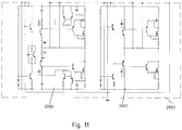
- Figure 11 displays an amplifier module 2003 adapted for coupling with the capacitor module of figure 10 .
- the amplifier module 2003 comprises two amplifiers, 2002 and 2007, of similar construction, for dissipation of the common mode noise component. These amplifier are preferably realized as hybrid circuits with SMD components on a Al2O3 substrate.
- the connection between the amplifier module and the capacitor module is done by a conventional electrical connector, or by other appropriate connection means.
Description
- Thispatent application relates to electrical filters for filtering an unwanted noise component from an electrical or electronic circuit or line and more particularly, but not exclusively, to electromagnetic compatibility filters for mains lines or distribution lines at mainsfrequency.
- Electromagnetic compatibility (EMC) isan increasingly critical factor in the electric and electronic industry now a days. A large number of electric circuits and appliances exist, which are liable to generate unwanted electrical noise, or to suffer from noise generated by other circuits or appliances.
- The conducted noises and disturbances are generally dealt with by inserting a low-pass LC filter on the mains supply line of the noise-generating devices or of the noise-sensitive devices. Such filters attenuate the unwanted frequency components to a harmless level. Many filter topologies, including the classic "L, "T" and "pi" filter topologies, can be employed.
- European Patent application
EP1069673 shows an example of a three-phase noise suppression filter comprising passive elements. - Passive EMCfilters have been proven effective in a number of applications. A shortcoming of this technique, however, is that in order to attain the required attenuation level, high-value capacitors and inductances are needed for this application. The size and cost of the resulting filter are mainly determined by these large components, in particular when high attenuation of common mode noise is needed. Moreover, the leakage current is directly proportional to the capacity of the filter capacitors.
- It is also known to employ active elements in noise suppression filters, for example as in European patent
EP0995266 . The use of active elements allows the use of smaller inductances and capacitors, thereby providing more compact filters. The existing active filters, however, remain less reliable than their traditional passive homologues, can fail due to overvoltage or overtemperature breakdown, or may exhibit instability and oscillations. -
US2004/008527 discloses an active power filter having capacitive coupling of noise. -
WO03/005578 - It is an aim of the present invention to provide an EMC filter which is more compact and reliable than the known devices.
- It is a further aim of the present invention to provide an EMC filter combining a high attenuation and a low leakage current.
- It is also an aim of the present invention to provide an EMC filter with a production cost lower than the known devices.
- These aims are attained by an EMC filter according to
claim 1, optional and additional useful features being introduced in the dependent claims. -
-
Figure 1 shows a schematic of an EMC filter according to a first aspect of the invention. -
Figure 2 shows a schematic of a portion of an EMC filter according to another aspect of the invention. -
Figures 3a to 3d show equivalent circuits useful to the stability analysis of the circuit of the invention. -
Figure 4 shows, in bloc diagrammatic form, an EMC active filter according to the invention. -
Figure 5 shows, in bloc diagrammatic form, an EMCactive filter according to an aspect of the invention. -
Figure 6 shows a variant of the filter offigure 5 according to another aspect of the invention. -
Figure 7 showsan active shunt module of the filter offigure 5 . -
Figure 8 shows, in bloc diagrammatic form, a modular EMCactive filter according to an aspect of the invention. -
Figure 9 displays, in diagrammatic form, a choke module of the filter offigure 8 . -
Figure 10 displays, in diagrammatic form, a capacitor module and a power supply module of the filter offigure 8 . -
Figure 11 displays, in diagrammatic form, an amplifier module of the filter offigure 8 . - Referring first to
Figure 4 , the filter circuit of the invention comprises at least one inductive part L1, L3 in series with each power line l1, l2, l3, l1', l2', l3' and oneactive shunt circuit 10 between each line and a current sink, for example the earth. The current to be filtered flows through each inductance from the mains supply line, on the left ofFigure 4 , to the load on the right ofFigure 4 . - The embodiment illustrated on
Figure 4 is built as a T-filter and comprises two current compensated inductances L1 and L3 and an active shunt between the middle point of the inductances and the earth. Theactive shunt 10 of the invention may however be used in other filter arrangements, for example in filter arrangements comprising only one inductance in series with each power line. The inductive part may comprise any combination of current compensated and not current compensated inductances in each line. - The
active shunt 10 acts as a capacitive bypass for attenuating high frequency voltage variations, notably noise, between the inductances L1 and L3. It comprises anamplifier 100, preferably a high-voltage; high-power operational amplifier, apassive network 101, a star-point circuit 102 and a DC floating power supply 103. - The star-
point circuit 102 includes passive elements, for example resistors and/or capacitors, connected between each line and a star-point 1010. The voltage at 1010 is fed to thepassive network 101 which may comprise, for example, an arrangement of capacitors and/or resistors The passive network is also connected to the reference point, for example to the earth point PE, and to the output of theoperational amplifier 100. Thepassive network 101 isarranged so asto reference one input of theamplifier 100 to the earth potential and the other input to the star-point 1010; the output of the operational amplifier isfed back to the inverting input of theamplifier 100 and to the capacitor C11. - In this way the
operational amplifier 100 continuously tries to keep theinput 1010 at the potential of the earth over the filter bandwidth. The current driven by theamplifier 100 in order to compensate for voltage variations at 1010 is fed from the power lines l1-l3 through the DC floating power supply 103. Thusany voltage variation at 1010 due to noise in the filter bandwidth will drive current from the power lines to earth through the power supply and the capacitor C11. - The DC power supply 103 of the invention comprises
rectifier 1031 for converting the AC power voltage available on lines L1-l3 into the DC supply voltages+Vs, -Vs, available to theoperational amplifier 100. - The DC power supply 103 of the invention further comprises a
voltage reducing circuit 1030 for reducing the DC voltage supplied to theamplifier 100 to a suitable level, and to reduce the power loss through this amplifier. - In a preferred embodiment, the DC power supply further comprises
security elements 1032 for protecting the amplifier against overvoltage, fast or important du/dt or di/dt variations, and/or for detecting and transmitting anomaly conditions. - The embodiment of the invention shown on
Figure 4 filters common mode noise on thestar point 1010. In a various embodiment (not shown), three active filters are used for filtering differential mode noise between each pair of power lines supplies. Each differential mode active filter preferably includes its DC power supply with a rectifier and a voltage reducing circuit, its ownoperational amplifier 100, and its ownpassive network 101. The differential mode active filters may further include common and/or independent anomaly conditions detections. The three common mode active filters may be used instead or in addition to the differential active filter ofFigure 1 . Voltage reducing circuit may be provided in the differential mode active filters but not in the common mode active filter, or just the opposite, on in both types of filters. -
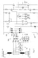
Figure 1 represents a more detailed schematic diagram of an example of EMC active filter according to the invention. Power is fed through the filter from each line l1-l3, l1'-l3' to load via two inductances, in this case via ferrite beads L1 and L2. A star-point system 102 comprises an X capacitor network C1 - C3 and bleed resistors R1-R3 to provide differential mode attenuation with assistance from stray line inductance. The X capacitor network also serves to make a solid RF connection to share common mode current between phases. The capacitor network comprises one capacitor C1 - C3 and one resistor between the connection point of the two inductances and one common point 1010which also serves as an input for the active portion of the filter. - C4 - C9 form a
voltage divider 1030 which serves to reduce the mains voltage to a level suitable for the active elements and which will also reduce power loss. Thedivider 1030 will also supply only a limited amount of power, for example 290 VAC on the output lines 1041-1043 instead of 400 VAC, with a limited maximum power so that in the event of a very large noise signal appearing, the voltage will collapse and thus the circuit will be protected from power overload. The voltage divider is advantageously made of capacitive elements for acting mainly on the higher frequency voltage components, for reducing the power losses, and for attenuating high frequency symmetric noise voltages. - The capacitive elements of the illustrated
voltage divider 1030 are connected in delta; a star connection, comprising one capacitor C4-C6 in series with each line 1041-1043 and a second capacitor between each line and a common point, is also possible. - In the illustrated example, the
voltage divider 1030 divides the AC voltage before rectification. Other types ofvoltage reducing circuits 1030 may be used for supplying the active portion of thefilter 1 with an adequate voltage. The voltage reduction circuit may also be combined with therectifier 1031. - Advantageously, the circuit of the invention does not include fuses. The
capacitive divider 1030 comprising, in this case, the capacitors C4-C9 limits the current to harmless levels, even in the case of a short circuit. By avoiding fuses, the stray inductance of the noise current path can be reduced. - A
rectifier 1031 comprising a bridge D1 - D6 provides a full rectification of the 3 phase mains and isused both for providing a DC supply +Vs, -Vs for the active filter circuit, and as a current path for the noise. - In the presented embodiment, the DC supply for the active part of the filter circuit is obtained by the
capacitive divider 1030 and the bridge of diodes D1-D6. Other rectifying means, for example an AC-DC converter, could also be used for this function and are comprised in the scope of the present invention. - The active portion of the
filter 1, which we will describe now, is arranged in order to continuously try to keep theinput 1010 at the potential of the earth. The current path includes the amplifier supplying lines+Vs, -Vsand the earth-connected capacitor C11, which acts in the bandwidth of the filter like a very low impedance element due to the active circuit. - R4 and D7 form a voltage reference for the current source Q3. This provides for example 1mA bias current to the differential pair Q1 and Q2 whose base terminals form the differential input to the complete amplifier. Q1 and Q2 share the current for current source Q3. The collector of Q1 is a current source which controls current to the positive rail. The collector of Q2 controls current to the negative rail via the current mirror Q4 and Q5.
- Q6 and Q9 form a complementary Darlington to drive positive current through C11 while Q7 and Q10 do the same for negative current. Q6 and Q7 are bias to about 1 mA, for example. Q9 and Q10 are bias for example to about 10mA by Q8 whose collector-emitter voltage can be set to just about two diode drops. Q1 input is biased via R23 to earth and R11/C10 is a feedback impedence. The circuit is arranged in such a way that C11 follows earth potential at low frequencies (say below 1kHz for example).
- Resistor / capacitor chains R19,R20,R21,R22,C12,C13,C14 and R24,R25,R26,C15,C16 are lag-lead networkswhich ensure a maximum leading base current of 45 degrees(see open loop analysis). C10 provides a dominant pole roll off at high frequencies (say above 500kHz). Note that the amplifier elements are all dc coupled and no bypass capacitors are used. This helps to ensure no unforeseen phase shifting which may induce resonance.
- The circuit 201 following the rectifier stages 1031 is equivalent, in this embodiment, to the combination of
elements figure 4 . - The stability of the circuit of
figure 1 will now be analyzed and discussed; the circuits shown onfigures 3a to 3d illustrate this explanation. - As visible on
figure 3b , representing the open loop behavior of the circuit, a voltage V1 is applied to amplifier input RC chain. The resulting base current (i) in Q1 and Q2 will be limited to a maximum of 45 degrees leading. The output current H*i is in phase with the input current, where H is the overall current gain. This output current passes through C11 resulting in V2 and effective impedance L of the power input, which includes L1 and the supply impedance (LISN) resulting in V3. If we ignore V2 for the moment, the stability criterion says that V3 must not be in phase with V1. - The maximum phase shift of V3 with respect to the output current (in the power input) will be 90 degrees leading (where L1 and LISN are purely inductive). Therefore, in the worst case V3 will lag V1 by 45 degrees (i.e. the phase margin is safe at 45 degrees). The voltage V2 always lags the output current by 90 degrees. It is only important at low frequencies where it follows earth potential. At higher frequencies it should be isolated from the base inputs.
- Referring now to the closed-loop equivalent circuit of
figure 3a , a noise current I is applied to L2. This current flows almost entirely via the amplifier output (H*i) and to earth via C11. The resulting input current (i) produces a shunt voltage V1 = Zin * i , where Zin is the impedance of the input RC chain. Put in terms of output current V1 = Zin * l / H. - Turning this around, Zs= V1 / lnoise = Zin / H, where Zs is the active shunt impedance. So the shunt impedance can be controlled by the ratio of Zin and H.
-
Figures 3c and 3d represent the behavior of the amplifier circuit of this embodiment in the case in which the internal feedback, respectively the external feedback are open. - Typically a shunt impedance of less than 100mR can be created. L1 serves to provide a further attenuation by forming a divider with the LISN.
-
Figure 2 represents another embodiment of a filter according to the invention. In this embodiment, only portions of the circuit downstream from the points+Vs and -Vs are changed; thevoltage divider 1030 andrectifier 1031 used for supplying a DC voltage +Vs, -Vs are similar to the corresponding elements shown onFigure 1 . - In the embodiment of
Figure 2 , the gain stages provided by the transistors Q1-Q10 are replaced by a high-voltage integrated, monolithicoperational amplifier 100. A fast, high-voltage and high-power operational amplifier is required for this application, preferably the operational amplifier should be based on the MOSFET technology. Bipolar circuits, however, are also possible within the framework of the present invention. The capacitive divider provided by C4-C9 onfigure 1 limits the risk of amplifier failure. - The inverting input -Vs of the
operational amplifier 100 is connected, for the frequency interval where the noise is expected, to the star-point 1010. The feedback acts in the sense of maintaining this point to a fixed potential, close to the reference potential. The current path is provided by theoperational amplifier 100 and the certified Y capacitor C11 connected to its output. In this way, the common-mode noise current circulates from the lines l1-l3, l1'-l3' via the impedances L1 or L2, the voltage dividing capacitors C4-C9, the bridge diodes D1-D6 onfigure 1 , the poweroperational amplifier 100 and the capacitor C11. - The effect of the active filter circuit is that the value of the capacitor C11 appears, at noise frequency, many times larger than the impedance of the capacitor itself, for example 100 times larger. A relatively small capacitor C11, with a little leakage and volume, can be employed.
- According to one aspect of the invention the
amplifier 100 and thenetwork 101 of theshunt module 10 may be seen as a transconductance amplifier, which has an output current dependent from the input voltage at thestar point 102. The transfer function isso chosen that very little current is drawn in the shunt module at DC or at mains frequency, while the shunt module has low impedance in the frequency range where noise attenuation is desired, typically between 130 kHz and 1 MHz. - Optimally the impedance in the attenuation range is real, in order to dissipate rapidly the energy of the noise component, without unwanted oscillations. Typically impedances of 1 ohm or less are obtained.
- Due to the very low impedance in the active filter, the impedances L1, L3 can be much lower than in a passive filter of equivalent performances, and these coils can be kept simple and small, for example they can consist of a straight wire section in a ferrite bead or in a suitable magnetic core, or can contain only a limited number of turns, for example only one or two turns, around a magnetic element, for example around a ring core. Current-compensated impedances, in which several phases are wound around a common core, are preferred.
- The voltage-clamping transzorbs D7 and D8 provide overvoltage and polarity-reversal protection, whereas the low-capacitance diodes D11-D13 are used for input protection, with a minimal power loss.
- Overloading or oscillation of the
operational amplifier 100 automatically implies a drop in its supply voltage, due to the power limitations imposed by the voltage divider C4-C9, thereby limiting the possible damages. The capacitor C11 is dimensioned to withstand the eventuality of a short circuit of the amplifier output, without the need of security fuses. The T-arrangement of the inductances L1 and L2 further reduces passive du/dt and di/dt values at the input of the amplifier. - The
active circuit section 1233 of this embodiment, as visible on figure 23, is equivalent to the combination ofelements figure 1 . - Other security features can be added in order to further protect the active filter of the invention against external disturbances, like for example lightning, RF disturbances, electrostatic discharges, electromagnetic pulses, and also against powerline anomalies, like overvoltages, missing phases etc.
- A further advantage of the device of the invention is that it does not include transformers at mains frequency or electrolytic capacitors, which are notoriously unreliable and subject to aging.
- The active filter of the invention preferably also comprises
elements 1032 for monitoring and detecting anomalous conditions, for example the collapse of the rail-to-rail voltage at the output of the bridge of diodes D1-D6, can be used to signal an anomalous condition like, for example, an oscillation or a component failure. An anomalous offset at the output or at the input of the amplifier could also be monitored for detecting a failure of a filter component. - In the event of an anomaly, detected for example by a variation in the supply voltage or in the output voltage of the operational amplifier, an appropriate signal may be sent out in order to trigger corrective actions. The circuit of the invention may comprise a light transducer, for example a LED, or an acoustic transducer, for example a loudspeaker or a buzzer, for emitting a luminous alarm signal or an acoustic alarm signals.
- The active filter can optionally include a signal output connection, for transmitting a status signal to a remote receiver. Such status signal may comprise, in a simple case, a simple "OK" flag, indicating that all the monitored parameters are within their respective safe ranges, or more elaborate data, providing detail on various operating parameters like current, power, voltage, noise level and temperature.
- Preferably, the signal output connection comprises an insulated output, for example a relay output, a photocoupler output, a light fiber output, or an interface for sending messages over a telecommunication network, for example over a wireless data network, a field network or a power line communication network. The remote receiver has thus the possibility to verify the correct functioning within prescribed operating limits of a number of EMC filters according to the invention.
- The remote receiver may be a part of a control system, which is set up to take adequate safety measures, in the event of an anomalous condition, like overload, overtemperature, or overvoltage, either according to an automatic program, or at the initiative of an operator.
- Optionally, the filter of the invention can provide means, for example a relay, to switch itself off autonomously in case of a detected anomaly, for example if power or temperature admissible functioning limits are exceeded, or in case of failure.
- Optionally, the DC voltage generated by the voltage divider C4-C9 and the bridge diodes D1-D6 can be used to generate an auxiliary voltage which is employed for supplying some of the filter's components, for example the monitoring and detection system described above.
- Advantageously, the auxiliary voltage so generated may be made available for powering components external to the filter, for example lamps, batteries, or other electronic circuitry. Preferably, the optional supply is made safe and stabilized to some standard value, like 5, 12, 24 or 48 V, by means of an appropriate DC-DC converter. Since the auxiliary voltage is galvanically isolated from the mains lines, thanks to the voltage divider C4-C9, the risk of failures and breakdowns is avoided.
- The filter of the invention may advantageously be employed as EMC suppressor at the input or output of frequency converters, as a network filter, or for any other device connected to a powerline.
- The illustrated embodiment shows a 3-phase filter circuit. Active monophase filters including a frequency divider and a rectifier according to the invention may also be built.
- The filter of the invention may also be employed on DC power lines, for example after the power supply in an electronic appliance, or in automotive applications.
- According to another aspect of the invention, represented in
figure 5 the filter comprises a first and a second inductive elements L1, L3, analogically to the previous embodiments, placed in series along the power lines l1, l2, l3, l1', l2', l3'. In addition to that, the filter of the invention also comprises additional inductive elements, L10, L20, whose function is to inductively couple the power lines and the shunt circuit, constituted by thepower supply 710, by the active modules702 and 703, which may be identical, and by thecapacitor bank 720. To this purpose the inductive elements L10 and L20 have secondary windings inductively linked to the power lines. - To simplify the realization, the turn ratio of L10 and L20 can be 1:1, which means that the emf voltage of the secondary windings equals that of the primary windings. The invention however is not limited to this particular turn ratio.
- In the example of
figure 5 the inductive element L10 hasa common magnetic circuit to which all the power lines and secondary winding are coupled and is arranged for maximal transfer of a common mode signal from the power lines to the shuntactive modules - At the same time inductive element L20 hasa separate magnetic circuit for each power line and is arranged to provide a shunt path for differential mode signals towards the
capacitor bank 720. Other disposition are however possible and comprised in the scope of the present invention. - Inductive elements L1, L3, L10 and L20 may be realized by means of magnetic cores, for example made of ferrite, permalloy, sintered metal or laminated steel, according to a variety of shapes and dispositions available in the art. In a particularly advantageous realization the inductive devices are obtained by passing the power cables into magnetic beads.
- The filter represented in
figure 5 isa two-stage low-pass filter with active shunt elements constituted byamplifiers second amplifier 702 behind the inductive device L10 is equivalent to connecting it between L1 and L10 via another bank of 'X' capacitors like in figure 6a, because the voltage drop on the secondary windings of L10 is equal or proportional to that present in the power conductors l1, l2, l3 when traversing L10. Thesecond shunt module 702 thus sees the same noise that it would experience if connected between L1 and L10 (with a multiplicative factor to the value of L10 in the case of a turn ratio different from unity). - In the same way connecting the
capacitors 720 at the secondary windings of the inductive device L20 is the same, in term of filter response, than placing thecapacitors bank 720 between L10 and L20. - The inductive device L10 create virtual shunt nodes H1, H2, H3, which are electrically equivalent to the section of the phase conductors l1, l2, l3, respectively, between the chokes L1 and L10. The inductive device L20 create virtual shunt nodes H4, H5, H6, which are electrically equivalent to the section of the phase conductors l1, l2, l3, respectively, between the chokes L20 and L10.
- By 'virtual shunt nodes' are intended, in this application, nodes of an electric network of a power filter, which are equivalent, for the purpose of connecting shunt elements, to a node of the power line to which they are inductively coupled.
- It will be appreciated that the inductively coupled shunt of the invention requires only one galvanic connection point G1, G2, G3 for each phase of the power cable, and only one bank of "X"
capacitors 750 for the coupling of the common mode filter stages provided byamplifiers -
Figure 7 shows an example of realization of thepower supply 710 and of theactive module 703. Thepower supply 710 comprises, like in the previous case, avoltage divider 711, capacitively realized, for reducing the voltage and current supplied to theactive modules 712 and 703. - The
active module 703, which is has the same layout as theactive module 702, comprise a power MOSFET output stage - The
active modules active modules - Optimally the impedance in the attenuation range is real, in order to dissipate rapidly the energy of the noise component, without unwanted oscillations. Typically impedances of 1 ohm or less are obtained.
- Due to the very low impedance module in the active filter, the impedances L1, L2 can be much lower than in a passive filter of equivalent performances, and these coils can be kept simple and small. The
active modules - With reference to
figure 6 , according to a variant of the invention the active modules702, 703 and the power supply have been replaced by afurther capacitor bank 730. This variant of the invention only includes passive elements and could be advantageous where a higher leakage current is tolerated. - According to another aspect of the invention, represented in
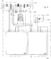
figure 8 , the filter is realized in a modular fashion, comprising achoke module 2001, a capacitor module, 2002, anamplifier module 2003 and an optionalpower supply module 2004. Thecapacitor module 2002 and theamplifier module 2003 correspond to the active shunt module of the previous embodiments. - With reference to the
figure 9 , thechoke module 2001 comprises a first and a second inductive elements L1, L3, analogically to the previous embodiments, placed in series along the power lines l1, l2, l3, l1', l2', l3'. In addition to that, thechoke module 2001 also comprises additional inductive elements, L10, L20, L30, whose function is to inductively couple the power lines and the shunt circuit, constituted thecapacitor module 2002 and by theamplifier module 2003. - In the example of
figures5 and 6 , the inductive element L10 and L30 are arranged for maximal transfer of a common mode signal from the power lines to the shunt circuit, whereas inductive element L2 does the same for differential mode signals. Other disposition are however possible and comprised in the scope of the present invention. - As before, the inductively coupled shunt of the invention requires only one galvanic connection point G1, G2, G3 for each phase of the power cable. This allows for a simpler and more reliable realization, particularly in the case of multi-stage filters, like the filter presented in this example. Advantageously the
choke module 2001 can adopt solid busbar conductors or insulated cables of adequate gauge for the phases l1, l2, l3. -
Figure 10 shows a capacitor module adapted for coupling with the choke module offigure 9 . The capacitor module includes the necessary coupling capacitors for transferring the noise signal to the amplifier module, as well as a bank of capacitor in star configuration for the attenuation of the differential mode noise. The capacitor module comprises, in this variant, apower supply module 2004 comprising a transformer whoseoutput 2010 is available for the supply of the amplifier modules or of other circuits - In this variant of the invention the supply of the amplifier is provided by a
separate transformer 2004 instead of a capacitive divider. This solution is preferable when the power dissipated in the active shunt modules is larger, for example in EMC filters for motors drives with long cables, which have to cope with large noise spikes. - Preferably the transformer used is a step-down transformer, which reduces the line voltage to same convenient value, in order to limit the voltage and power requirement to the active modules.
- In power supply module the +Ve and -Ve are imposed between two star points of two identical RC star networks, the two networks forming a three-phase bridge. This way the DCvoltage is completely isolated from the AC and vice versa. Also the DC module plays no role in the filtering function of the circuit, the noise being separately transmitted to the SP inputs of the amplifiers.
- Preferably the capacitor module is realized on a PCB (Printed Circuit Board) for a simple and economical assembly by conventional soldering techniques. It should be noted that the capacitor module does not have to handle the rated currents at mains frequency. The connection between the
choke module 2001 and the capacitor module can be realized by soldering, crimping, or by an electric connector of adequate voltage and current capability. Given the relatively low level of current involved, this connection poses little reliability concerns. -
Figure 11 displays anamplifier module 2003 adapted for coupling with the capacitor module offigure 10 . Theamplifier module 2003 comprises two amplifiers, 2002 and 2007, of similar construction, for dissipation of the common mode noise component. These amplifier are preferably realized as hybrid circuits with SMD components on a Al2O3 substrate. The connection between the amplifier module and the capacitor module is done by a conventional electrical connector, or by other appropriate connection means.
Claims (18)
- EMC filter, for connection between a three-pase supply network (l1, l2, l3) and an electric operated appliance (l1', l2', l3') to reduce conduction noise between said supply network (l1, l2, l3) and said appliance (l1', l2', l3'), comprising:a rectifier (1031), for converting an AC voltage into a DC voltage,an electronic active circuit, supplied by said DC voltage, for absorbing a noise current transmitted between said supply network (l1, l2, l3) and said appliance (l1', l2', l3'),
characterized bya voltage reducing circuit (1030) comprising a voltage divider made up of capacitors (C4, C5, C6, C7, C8, C9), wherein said voltage reducing circuit (1030) is connected to said supply network (l1, l2, l3) and is configured to supply to said rectifier (1031) an AC voltage lower than an AC voltage of said supply network (l1, l2, l3). - The filter of one of the preceding claims, wherein said voltage reducing circuit (1030) is made up of delta-connected passive elements (C7, C8, C9).
- The filter of one of the preceding claims, wherein said rectifier (1031) comprises a bridge of diodes (D1, D2, D3, D4, D5, D6).
- The filter of one of the claims 1 to 3, wherein said rectifier (1031) comprises an AC-DC converter.
- The filter of one of the preceding claims, wherein said electronic active circuit comprises an integrated operational amplifier (100).
- The filter of the preceding claim, wherein said operational amplifier (100) is a MOSFET amplifier.
- The filter of one of the preceding claims, further comprising security elements (1032) for protecting the amplifier (100) against overvoltages, fast or important du/dt or di/dt variations, and/or for detecting and transmitting anomaly conditions.
- The filter of one of the preceding claims, wherein said operational amplifier (100) is a MOSFET amplifier, further comprising a supply output connector, connected to said DC voltage.
- The filter of the preceding claim, further comprising an isolated DC-DC converter, said supply output connector being connected to an output of said DC-DC converter.
- The filter of one of the preceding claims, further comprising a star-point circuit (102) including passive elements (C1, R1; C2, R2; C3, R3) connected between each power supply line of said supply network and a star-point, wherein the current flowing through said electronic active circuit depends on the potential on said star-point circuit (102).
- The filter of one of the preceding claims, comprising at least one inductive device (L10, L20) connected to power supply lines in a manner to transfer inductively the noise current to the electronic active circuit.
- The filter of the preceding claim, in which said inductive device (L10, L20) comprises secondary windings, inductively coupled to the power supply lines.
- The filter of the preceding claim, in which said inductive device (L10, L20) comprises a common magnetic circuit coupled to all phases of the power supply lines, for coupling a common mode noise current.
- The filter of claim 12, in which said inductive device (L10, L20) comprises independent magnetic circuits individually coupled to each phase of the power supply lines, for coupling a differential mode noise current.
- The filter of one of the preceding claims, wherein the electronic active circuit is connected to a virtual shunt node (H1-H6) inductively associated to a node of the conductors lines (l1, l2, l3) of the supply network.
- A system comprising a supply network (l1, l2, l3), an electric operated appliance (l1', l2', l3'), three power supply lines connected between the supply network (l1, l2, l3) and the electric operated appliance (l1', l2', l3'), at least one inductive part (L1, L3) in series with each power supply line and an EMC filter according to anyone of claims 1 to 16 connected between the tree power supply lines and a current sink.
- The system according to claim 17, wherein the at least one inductive part (L1, L3) in series with each power supply line comprises two inductive parts (L1, L3) in series with each power supply line, wherein the said voltage reducing circuit (1030) of said EMC filter is connected to said three power supply lines.
- The system according to claim 16 or 17, wherein the EMC filter is connected between the power supply lines and the earth.
Applications Claiming Priority (2)
| Application Number | Priority Date | Filing Date | Title |
|---|---|---|---|
| US59033604P | 2004-07-23 | 2004-07-23 | |
| PCT/EP2005/053613 WO2006008322A2 (en) | 2004-07-23 | 2005-07-25 | Emc filter |
Publications (2)
| Publication Number | Publication Date |
|---|---|
| EP1774652A2 EP1774652A2 (en) | 2007-04-18 |
| EP1774652B1 true EP1774652B1 (en) | 2017-04-26 |
Family
ID=35478287
Family Applications (2)
| Application Number | Title | Priority Date | Filing Date |
|---|---|---|---|
| EP05106806A Ceased EP1619768A1 (en) | 2004-07-23 | 2005-07-25 | Filter with virtual shunt nodes |
| EP05769892.0A Active EP1774652B1 (en) | 2004-07-23 | 2005-07-25 | Emc filter |
Family Applications Before (1)
| Application Number | Title | Priority Date | Filing Date |
|---|---|---|---|
| EP05106806A Ceased EP1619768A1 (en) | 2004-07-23 | 2005-07-25 | Filter with virtual shunt nodes |
Country Status (3)
| Country | Link |
|---|---|
| US (1) | US7667988B2 (en) |
| EP (2) | EP1619768A1 (en) |
| WO (1) | WO2006008322A2 (en) |
Families Citing this family (25)
| Publication number | Priority date | Publication date | Assignee | Title |
|---|---|---|---|---|
| US7154254B2 (en) * | 2004-06-18 | 2006-12-26 | Agilent Technologies, Inc. | Apparatus and method for improving electromagnetic compatibility |
| US20070025109A1 (en) * | 2005-07-26 | 2007-02-01 | Yu Jing J | C7, C9 LED bulb and embedded PCB circuit board |
| US20080048779A1 (en) * | 2006-05-16 | 2008-02-28 | Crawley Philip J | Active emi suppression circuit |
| DE112007001565B4 (en) | 2006-08-15 | 2018-01-25 | Schaffner Emv Ag | EMC filter with low leakage current |
| EP2800285B1 (en) * | 2006-08-24 | 2019-10-02 | Sony Deutschland Gmbh | Method for transmitting a signal on a power line network, transmitting unit, receiving unit and system |
| US7764041B2 (en) * | 2007-01-22 | 2010-07-27 | Johnson Controls Technology Company | System and method to extend synchronous operation of an active converter in a variable speed drive |
| WO2009046762A1 (en) * | 2007-10-10 | 2009-04-16 | Schaffner Emv Ag | Emc filter |
| US8174853B2 (en) * | 2007-10-30 | 2012-05-08 | Johnson Controls Technology Company | Variable speed drive |
| US7957166B2 (en) * | 2007-10-30 | 2011-06-07 | Johnson Controls Technology Company | Variable speed drive |
| DE102008031536A1 (en) * | 2008-07-03 | 2010-01-14 | Fujitsu Technology Solutions Gmbh | Circuit arrangement and drive circuit for a power supply, computer power supply and method for switching a power supply |
| ATE543266T1 (en) * | 2008-08-20 | 2012-02-15 | Sony Corp | DEVICE FOR DETERMINING A COMMON MODE SIGNAL IN A POWER LINE COMMUNICATION NETWORK |
| DE102009037859B4 (en) * | 2009-08-18 | 2017-02-23 | Fujitsu Technology Solutions Intellectual Property Gmbh | Input circuit for an electrical device, use of an input circuit and electrical device |
| US8542364B1 (en) * | 2009-12-17 | 2013-09-24 | Honeywell International Inc. | System to reduce gyroscopic errors with limited power supply quality in a fiber optic gyroscope |
| US8325501B2 (en) * | 2010-05-24 | 2012-12-04 | Huawei Technologies Co., Ltd. | Method and device of electrical power |
| FR2971886B1 (en) * | 2011-02-21 | 2014-01-10 | Nanotec Solution | DEVICE AND METHOD FOR INTERCONNECTING ELECTRONIC SYSTEMS TO DIFFERENT REFERENCE POTENTIALS |
| US8861145B2 (en) | 2012-07-19 | 2014-10-14 | Honeywell International Inc. | Circuit with motor driver spike suppression |
| GB2504494A (en) * | 2012-07-30 | 2014-02-05 | Eaton Aerospace Ltd | Phase loss or input voltage drop detection using common-mode voltage in rectified signal |
| US9559581B2 (en) * | 2013-04-17 | 2017-01-31 | The Regents Of The University Of Michigan | Single phase bi-directional AC-DC converter with reduced passive components size and common mode electro-magnetic interference |
| JP2014241711A (en) * | 2013-04-19 | 2014-12-25 | シャフナー・エーエムファウ・アクチェンゲゼルシャフト | Active EMC filter |
| US9977858B2 (en) | 2014-07-03 | 2018-05-22 | The Boeing Company | Electromagnetic interference filters for power converter applications |
| EP3073624A1 (en) * | 2015-03-27 | 2016-09-28 | Siemens Aktiengesellschaft | Mains filter for converter |
| CN109638935A (en) * | 2017-10-06 | 2019-04-16 | 保时捷股份公司 | Use of two DC/DC adjusters in the power electronic equipment at charging station or power-up station |
| NL2019705B1 (en) * | 2017-10-11 | 2019-04-19 | Van Bommel Johan | Compensating apparatus for reducing leakage current |
| DE102019112598A1 (en) * | 2019-05-14 | 2020-11-19 | Dr. Johannes Heidenhain Gmbh | High frequency line filter |
| CN110943707A (en) * | 2019-12-19 | 2020-03-31 | Tcl华星光电技术有限公司 | Filter circuit and electronic device |
Citations (1)
| Publication number | Priority date | Publication date | Assignee | Title |
|---|---|---|---|---|
| US4369490A (en) * | 1979-12-14 | 1983-01-18 | Patent-Treuhand-Gesellschaft Fur Elektrische Gluhlampen | Low-ripple power rectifier system |
Family Cites Families (14)
| Publication number | Priority date | Publication date | Assignee | Title |
|---|---|---|---|---|
| US4402028A (en) * | 1981-08-17 | 1983-08-30 | Electric Power Research Institute, Inc. | Protective relay methods and apparatus |
| US5319535A (en) * | 1993-08-19 | 1994-06-07 | Westinghouse Electric Corp. | Active power line conditioner having capability for rejection of common-mode disturbances |
| US5666255A (en) | 1995-06-05 | 1997-09-09 | Powervar, Inc. | Transformerless conditioning of a power distribution system |
| GB9713878D0 (en) | 1997-06-30 | 1997-09-03 | Roxburgh Electronics Ltd | Mains filtering circuit |
| US5905642A (en) * | 1997-11-11 | 1999-05-18 | Robicon Corporation | Apparatus and method to reduce common mode voltage from current source drives |
| US6122183A (en) * | 1998-11-24 | 2000-09-19 | Lucent Technologies Inc. | Two-stage, three-phase boost converter with reduced total harmonic distortion |
| DE59912896D1 (en) | 1999-07-16 | 2006-01-12 | Schaffner Emv Ag Luterbach | Line filter |
| US6130832A (en) * | 1999-11-08 | 2000-10-10 | Otis Elevator Company | Active filtering of AC/DC switched converter input current |
| US6839249B2 (en) * | 2001-01-10 | 2005-01-04 | Honeywell International Inc. | AC-to-ac power converter without a dc link capacitor |
| US6690230B2 (en) | 2001-05-17 | 2004-02-10 | International Rectifier Corporation | Active common mode filter connected in A-C line |
| KR100403541B1 (en) * | 2001-06-29 | 2003-10-30 | 설승기 | Active Common Mode EMI Filter for Eliminating Conducted Electromagnetic Interference |
| JP4034733B2 (en) | 2002-01-07 | 2008-01-16 | インターナショナル レクティフィアー コーポレイション | Active EMI filter with feedforward cancellation |
| US6781444B2 (en) * | 2002-05-22 | 2004-08-24 | International Rectifier Corporation | Active common mode EMI filter, including series cascaded filter with reduced power dissipation and transistor voltage rating |
| US6775157B2 (en) * | 2002-06-25 | 2004-08-10 | International Rectifier Corporation | Closed loop active EMI filter for reducing common or differential noise based on an error value |
-
2005
- 2005-07-25 WO PCT/EP2005/053613 patent/WO2006008322A2/en active Application Filing
- 2005-07-25 EP EP05106806A patent/EP1619768A1/en not_active Ceased
- 2005-07-25 EP EP05769892.0A patent/EP1774652B1/en active Active
-
2007
- 2007-01-03 US US11/619,510 patent/US7667988B2/en active Active
Patent Citations (1)
| Publication number | Priority date | Publication date | Assignee | Title |
|---|---|---|---|---|
| US4369490A (en) * | 1979-12-14 | 1983-01-18 | Patent-Treuhand-Gesellschaft Fur Elektrische Gluhlampen | Low-ripple power rectifier system |
Also Published As
| Publication number | Publication date |
|---|---|
| US20070159860A1 (en) | 2007-07-12 |
| EP1619768A1 (en) | 2006-01-25 |
| WO2006008322A2 (en) | 2006-01-26 |
| EP1774652A2 (en) | 2007-04-18 |
| US7667988B2 (en) | 2010-02-23 |
| WO2006008322A3 (en) | 2006-12-28 |
Similar Documents
| Publication | Publication Date | Title |
|---|---|---|
| EP1774652B1 (en) | Emc filter | |
| CN101897109B (en) | Emc filter | |
| JP6485662B2 (en) | Common mode filter device and electrical equipment | |
| US7659797B2 (en) | Low-leakage EMC filter | |
| US7724549B2 (en) | Integrated power conditioning system and housing for delivering operational power to a motor | |
| CN1744450B (en) | Serial signal injection using capacitive and transformer couplings for power line communications | |
| JP2004534500A (en) | Active Common Mode EMI Filter for Eliminating Conducted Electromagnetic Interference for Eliminating Impedance of Conducted Electromagnetic Devices | |
| EP2876794B1 (en) | Input EMI filter and method for motor drive including an active rectifier | |
| KR20210129135A (en) | Device and method for filtering electromagnetic interference | |
| EP3553935B1 (en) | Power conversion device | |
| US7535125B2 (en) | Single-phase filter for reducing harmonics | |
| JP2005204438A (en) | Noise filter | |
| WO2014048471A1 (en) | Power line filter device | |
| JP2020103029A (en) | Motor drive with filter including three-phase differential mode reactor exhibiting common mode damping | |
| US20050140460A1 (en) | Power conditioners and pseudo isolation for a two-wire processing network | |
| CN114977774A (en) | Drive circuit with EMI restraines and car motor drive system | |
| US10886857B1 (en) | Inhibiting noise coupling across isolated power supplies | |
| US10277277B2 (en) | ULF/VLF power line communications coupler | |
| EP4203221A1 (en) | Electromagnetic interference filter | |
| JP6828839B2 (en) | Switching power supply | |
| CN214674872U (en) | DC output end conduction filter circuit applied to POE power supply | |
| JP2018510607A (en) | Filter for converter |
Legal Events
| Date | Code | Title | Description |
|---|---|---|---|
| PUAI | Public reference made under article 153(3) epc to a published international application that has entered the european phase |
Free format text: ORIGINAL CODE: 0009012 |
|
| 17P | Request for examination filed |
Effective date: 20070104 |
|
| AK | Designated contracting states |
Kind code of ref document: A2 Designated state(s): AT BE BG CH CY CZ DE DK EE ES FI FR GB GR HU IE IS IT LI LT LU LV MC NL PL PT RO SE SI SK TR |
|
| AX | Request for extension of the european patent |
Extension state: AL BA HR MK YU |
|
| DAX | Request for extension of the european patent (deleted) | ||
| 17Q | First examination report despatched |
Effective date: 20100901 |
|
| GRAP | Despatch of communication of intention to grant a patent |
Free format text: ORIGINAL CODE: EPIDOSNIGR1 |
|
| INTG | Intention to grant announced |
Effective date: 20161107 |
|
| GRAS | Grant fee paid |
Free format text: ORIGINAL CODE: EPIDOSNIGR3 |
|
| GRAJ | Information related to disapproval of communication of intention to grant by the applicant or resumption of examination proceedings by the epo deleted |
Free format text: ORIGINAL CODE: EPIDOSDIGR1 |
|
| GRAL | Information related to payment of fee for publishing/printing deleted |
Free format text: ORIGINAL CODE: EPIDOSDIGR3 |
|
| GRAP | Despatch of communication of intention to grant a patent |
Free format text: ORIGINAL CODE: EPIDOSNIGR1 |
|
| GRAA | (expected) grant |
Free format text: ORIGINAL CODE: 0009210 |
|
| INTC | Intention to grant announced (deleted) | ||
| INTG | Intention to grant announced |
Effective date: 20170314 |
|
| AK | Designated contracting states |
Kind code of ref document: B1 Designated state(s): AT BE BG CH CY CZ DE DK EE ES FI FR GB GR HU IE IS IT LI LT LU LV MC NL PL PT RO SE SI SK TR |
|
| REG | Reference to a national code |
Ref country code: GB Ref legal event code: FG4D |
|
| REG | Reference to a national code |
Ref country code: CH Ref legal event code: EP |
|
| REG | Reference to a national code |
Ref country code: AT Ref legal event code: REF Ref document number: 888673 Country of ref document: AT Kind code of ref document: T Effective date: 20170515 |
|
| REG | Reference to a national code |
Ref country code: IE Ref legal event code: FG4D |
|
| REG | Reference to a national code |
Ref country code: DE Ref legal event code: R096 Ref document number: 602005051830 Country of ref document: DE |
|
| REG | Reference to a national code |
Ref country code: NL Ref legal event code: MP Effective date: 20170426 |
|
| REG | Reference to a national code |
Ref country code: LT Ref legal event code: MG4D |
|
| REG | Reference to a national code |
Ref country code: AT Ref legal event code: MK05 Ref document number: 888673 Country of ref document: AT Kind code of ref document: T Effective date: 20170426 |
|
| PG25 | Lapsed in a contracting state [announced via postgrant information from national office to epo] |
Ref country code: NL Free format text: LAPSE BECAUSE OF FAILURE TO SUBMIT A TRANSLATION OF THE DESCRIPTION OR TO PAY THE FEE WITHIN THE PRESCRIBED TIME-LIMIT Effective date: 20170426 |
|
| PG25 | Lapsed in a contracting state [announced via postgrant information from national office to epo] |
Ref country code: FI Free format text: LAPSE BECAUSE OF FAILURE TO SUBMIT A TRANSLATION OF THE DESCRIPTION OR TO PAY THE FEE WITHIN THE PRESCRIBED TIME-LIMIT Effective date: 20170426 Ref country code: ES Free format text: LAPSE BECAUSE OF FAILURE TO SUBMIT A TRANSLATION OF THE DESCRIPTION OR TO PAY THE FEE WITHIN THE PRESCRIBED TIME-LIMIT Effective date: 20170426 Ref country code: GR Free format text: LAPSE BECAUSE OF FAILURE TO SUBMIT A TRANSLATION OF THE DESCRIPTION OR TO PAY THE FEE WITHIN THE PRESCRIBED TIME-LIMIT Effective date: 20170727 Ref country code: LT Free format text: LAPSE BECAUSE OF FAILURE TO SUBMIT A TRANSLATION OF THE DESCRIPTION OR TO PAY THE FEE WITHIN THE PRESCRIBED TIME-LIMIT Effective date: 20170426 Ref country code: AT Free format text: LAPSE BECAUSE OF FAILURE TO SUBMIT A TRANSLATION OF THE DESCRIPTION OR TO PAY THE FEE WITHIN THE PRESCRIBED TIME-LIMIT Effective date: 20170426 |
|
| PG25 | Lapsed in a contracting state [announced via postgrant information from national office to epo] |
Ref country code: PL Free format text: LAPSE BECAUSE OF FAILURE TO SUBMIT A TRANSLATION OF THE DESCRIPTION OR TO PAY THE FEE WITHIN THE PRESCRIBED TIME-LIMIT Effective date: 20170426 Ref country code: BG Free format text: LAPSE BECAUSE OF FAILURE TO SUBMIT A TRANSLATION OF THE DESCRIPTION OR TO PAY THE FEE WITHIN THE PRESCRIBED TIME-LIMIT Effective date: 20170726 Ref country code: IS Free format text: LAPSE BECAUSE OF FAILURE TO SUBMIT A TRANSLATION OF THE DESCRIPTION OR TO PAY THE FEE WITHIN THE PRESCRIBED TIME-LIMIT Effective date: 20170826 Ref country code: SE Free format text: LAPSE BECAUSE OF FAILURE TO SUBMIT A TRANSLATION OF THE DESCRIPTION OR TO PAY THE FEE WITHIN THE PRESCRIBED TIME-LIMIT Effective date: 20170426 Ref country code: LV Free format text: LAPSE BECAUSE OF FAILURE TO SUBMIT A TRANSLATION OF THE DESCRIPTION OR TO PAY THE FEE WITHIN THE PRESCRIBED TIME-LIMIT Effective date: 20170426 |
|
| REG | Reference to a national code |
Ref country code: DE Ref legal event code: R097 Ref document number: 602005051830 Country of ref document: DE |
|
| PG25 | Lapsed in a contracting state [announced via postgrant information from national office to epo] |
Ref country code: RO Free format text: LAPSE BECAUSE OF FAILURE TO SUBMIT A TRANSLATION OF THE DESCRIPTION OR TO PAY THE FEE WITHIN THE PRESCRIBED TIME-LIMIT Effective date: 20170426 Ref country code: EE Free format text: LAPSE BECAUSE OF FAILURE TO SUBMIT A TRANSLATION OF THE DESCRIPTION OR TO PAY THE FEE WITHIN THE PRESCRIBED TIME-LIMIT Effective date: 20170426 Ref country code: DK Free format text: LAPSE BECAUSE OF FAILURE TO SUBMIT A TRANSLATION OF THE DESCRIPTION OR TO PAY THE FEE WITHIN THE PRESCRIBED TIME-LIMIT Effective date: 20170426 Ref country code: CZ Free format text: LAPSE BECAUSE OF FAILURE TO SUBMIT A TRANSLATION OF THE DESCRIPTION OR TO PAY THE FEE WITHIN THE PRESCRIBED TIME-LIMIT Effective date: 20170426 Ref country code: SK Free format text: LAPSE BECAUSE OF FAILURE TO SUBMIT A TRANSLATION OF THE DESCRIPTION OR TO PAY THE FEE WITHIN THE PRESCRIBED TIME-LIMIT Effective date: 20170426 |
|
| PG25 | Lapsed in a contracting state [announced via postgrant information from national office to epo] |
Ref country code: IT Free format text: LAPSE BECAUSE OF FAILURE TO SUBMIT A TRANSLATION OF THE DESCRIPTION OR TO PAY THE FEE WITHIN THE PRESCRIBED TIME-LIMIT Effective date: 20170426 |
|
| REG | Reference to a national code |
Ref country code: CH Ref legal event code: PL |
|
| PLBE | No opposition filed within time limit |
Free format text: ORIGINAL CODE: 0009261 |
|
| STAA | Information on the status of an ep patent application or granted ep patent |
Free format text: STATUS: NO OPPOSITION FILED WITHIN TIME LIMIT |
|
| GBPC | Gb: european patent ceased through non-payment of renewal fee |
Effective date: 20170726 |
|
| 26N | No opposition filed |
Effective date: 20180129 |
|
| REG | Reference to a national code |
Ref country code: IE Ref legal event code: MM4A |
|
| REG | Reference to a national code |
Ref country code: FR Ref legal event code: ST Effective date: 20180330 |
|
| PG25 | Lapsed in a contracting state [announced via postgrant information from national office to epo] |
Ref country code: IE Free format text: LAPSE BECAUSE OF NON-PAYMENT OF DUE FEES Effective date: 20170725 Ref country code: LI Free format text: LAPSE BECAUSE OF NON-PAYMENT OF DUE FEES Effective date: 20170731 Ref country code: GB Free format text: LAPSE BECAUSE OF NON-PAYMENT OF DUE FEES Effective date: 20170726 Ref country code: CH Free format text: LAPSE BECAUSE OF NON-PAYMENT OF DUE FEES Effective date: 20170731 |
|
| PG25 | Lapsed in a contracting state [announced via postgrant information from national office to epo] |
Ref country code: SI Free format text: LAPSE BECAUSE OF FAILURE TO SUBMIT A TRANSLATION OF THE DESCRIPTION OR TO PAY THE FEE WITHIN THE PRESCRIBED TIME-LIMIT Effective date: 20170426 Ref country code: FR Free format text: LAPSE BECAUSE OF NON-PAYMENT OF DUE FEES Effective date: 20170731 |
|
| REG | Reference to a national code |
Ref country code: BE Ref legal event code: MM Effective date: 20170731 |
|
| PG25 | Lapsed in a contracting state [announced via postgrant information from national office to epo] |
Ref country code: LU Free format text: LAPSE BECAUSE OF NON-PAYMENT OF DUE FEES Effective date: 20170725 |
|
| PG25 | Lapsed in a contracting state [announced via postgrant information from national office to epo] |
Ref country code: BE Free format text: LAPSE BECAUSE OF NON-PAYMENT OF DUE FEES Effective date: 20170731 |
|
| PG25 | Lapsed in a contracting state [announced via postgrant information from national office to epo] |
Ref country code: HU Free format text: LAPSE BECAUSE OF FAILURE TO SUBMIT A TRANSLATION OF THE DESCRIPTION OR TO PAY THE FEE WITHIN THE PRESCRIBED TIME-LIMIT; INVALID AB INITIO Effective date: 20050725 Ref country code: MC Free format text: LAPSE BECAUSE OF FAILURE TO SUBMIT A TRANSLATION OF THE DESCRIPTION OR TO PAY THE FEE WITHIN THE PRESCRIBED TIME-LIMIT Effective date: 20170426 |
|
| PG25 | Lapsed in a contracting state [announced via postgrant information from national office to epo] |
Ref country code: CY Free format text: LAPSE BECAUSE OF NON-PAYMENT OF DUE FEES Effective date: 20170426 |
|
| REG | Reference to a national code |
Ref country code: DE Ref legal event code: R082 Ref document number: 602005051830 Country of ref document: DE Representative=s name: BECK & ROESSIG EUROPEAN PATENT ATTORNEYS, DE Ref country code: DE Ref legal event code: R082 Ref document number: 602005051830 Country of ref document: DE Representative=s name: BECK & ROESSIG - EUROPEAN PATENT ATTORNEYS, DE |
|
| PG25 | Lapsed in a contracting state [announced via postgrant information from national office to epo] |
Ref country code: TR Free format text: LAPSE BECAUSE OF FAILURE TO SUBMIT A TRANSLATION OF THE DESCRIPTION OR TO PAY THE FEE WITHIN THE PRESCRIBED TIME-LIMIT Effective date: 20170426 |
|
| PG25 | Lapsed in a contracting state [announced via postgrant information from national office to epo] |
Ref country code: PT Free format text: LAPSE BECAUSE OF FAILURE TO SUBMIT A TRANSLATION OF THE DESCRIPTION OR TO PAY THE FEE WITHIN THE PRESCRIBED TIME-LIMIT Effective date: 20170426 |
|
| PGFP | Annual fee paid to national office [announced via postgrant information from national office to epo] |
Ref country code: DE Payment date: 20230719 Year of fee payment: 19 |