EP1936672A1 - Electron blocking layers for gate stacks of nonvolatile memory devices - Google Patents
Electron blocking layers for gate stacks of nonvolatile memory devices Download PDFInfo
- Publication number
- EP1936672A1 EP1936672A1 EP07252410A EP07252410A EP1936672A1 EP 1936672 A1 EP1936672 A1 EP 1936672A1 EP 07252410 A EP07252410 A EP 07252410A EP 07252410 A EP07252410 A EP 07252410A EP 1936672 A1 EP1936672 A1 EP 1936672A1
- Authority
- EP
- European Patent Office
- Prior art keywords
- layer
- dielectric layer
- gate stack
- dielectric
- control
- Prior art date
- Legal status (The legal status is an assumption and is not a legal conclusion. Google has not performed a legal analysis and makes no representation as to the accuracy of the status listed.)
- Ceased
Links
- 230000000903 blocking effect Effects 0.000 title claims description 174
- 238000003860 storage Methods 0.000 claims abstract description 158
- 239000003989 dielectric material Substances 0.000 claims abstract description 59
- 230000015654 memory Effects 0.000 claims abstract description 57
- 238000000034 method Methods 0.000 claims abstract description 35
- CJNBYAVZURUTKZ-UHFFFAOYSA-N hafnium(iv) oxide Chemical compound O=[Hf]=O CJNBYAVZURUTKZ-UHFFFAOYSA-N 0.000 claims abstract description 8
- 230000005641 tunneling Effects 0.000 claims description 75
- VYPSYNLAJGMNEJ-UHFFFAOYSA-N Silicium dioxide Chemical compound O=[Si]=O VYPSYNLAJGMNEJ-UHFFFAOYSA-N 0.000 claims description 63
- 239000000758 substrate Substances 0.000 claims description 33
- 229910052681 coesite Inorganic materials 0.000 claims description 32
- 229910052906 cristobalite Inorganic materials 0.000 claims description 32
- 239000000377 silicon dioxide Substances 0.000 claims description 32
- 229910052682 stishovite Inorganic materials 0.000 claims description 32
- 229910052905 tridymite Inorganic materials 0.000 claims description 32
- 150000004767 nitrides Chemical class 0.000 claims description 29
- 229910052751 metal Inorganic materials 0.000 claims description 27
- 239000002184 metal Substances 0.000 claims description 27
- 239000002159 nanocrystal Substances 0.000 claims description 22
- 229910052735 hafnium Inorganic materials 0.000 claims description 16
- 230000005684 electric field Effects 0.000 claims description 15
- VBJZVLUMGGDVMO-UHFFFAOYSA-N hafnium atom Chemical compound [Hf] VBJZVLUMGGDVMO-UHFFFAOYSA-N 0.000 claims description 15
- 150000001875 compounds Chemical class 0.000 claims description 12
- 229910016909 AlxOy Inorganic materials 0.000 claims description 6
- 238000004519 manufacturing process Methods 0.000 claims description 5
- PNEYBMLMFCGWSK-UHFFFAOYSA-N aluminium oxide Inorganic materials [O-2].[O-2].[O-2].[Al+3].[Al+3] PNEYBMLMFCGWSK-UHFFFAOYSA-N 0.000 claims description 3
- 229910020781 SixOy Inorganic materials 0.000 claims 2
- 229910052593 corundum Inorganic materials 0.000 claims 2
- 229910001845 yogo sapphire Inorganic materials 0.000 claims 2
- TWNQGVIAIRXVLR-UHFFFAOYSA-N oxo(oxoalumanyloxy)alumane Chemical compound O=[Al]O[Al]=O TWNQGVIAIRXVLR-UHFFFAOYSA-N 0.000 abstract description 29
- 230000014759 maintenance of location Effects 0.000 abstract description 12
- 239000002105 nanoparticle Substances 0.000 abstract description 9
- MIQVEZFSDIJTMW-UHFFFAOYSA-N aluminum hafnium(4+) oxygen(2-) Chemical compound [O-2].[Al+3].[Hf+4] MIQVEZFSDIJTMW-UHFFFAOYSA-N 0.000 abstract description 2
- 239000010410 layer Substances 0.000 description 517
- 229910000449 hafnium oxide Inorganic materials 0.000 description 50
- 230000004888 barrier function Effects 0.000 description 31
- IJGRMHOSHXDMSA-UHFFFAOYSA-N Atomic nitrogen Chemical compound N#N IJGRMHOSHXDMSA-UHFFFAOYSA-N 0.000 description 28
- 239000000463 material Substances 0.000 description 25
- 239000000203 mixture Substances 0.000 description 22
- 229910052757 nitrogen Inorganic materials 0.000 description 14
- XUIMIQQOPSSXEZ-UHFFFAOYSA-N Silicon Chemical compound [Si] XUIMIQQOPSSXEZ-UHFFFAOYSA-N 0.000 description 13
- 229910052710 silicon Inorganic materials 0.000 description 13
- 239000010703 silicon Substances 0.000 description 13
- 238000000231 atomic layer deposition Methods 0.000 description 12
- 238000005229 chemical vapour deposition Methods 0.000 description 11
- 238000000151 deposition Methods 0.000 description 11
- 238000005240 physical vapour deposition Methods 0.000 description 11
- 239000002096 quantum dot Substances 0.000 description 11
- 238000004088 simulation Methods 0.000 description 11
- 239000004065 semiconductor Substances 0.000 description 10
- MCMNRKCIXSYSNV-UHFFFAOYSA-N Zirconium dioxide Chemical compound O=[Zr]=O MCMNRKCIXSYSNV-UHFFFAOYSA-N 0.000 description 8
- 239000010408 film Substances 0.000 description 8
- 230000008569 process Effects 0.000 description 8
- 230000008901 benefit Effects 0.000 description 7
- 230000008021 deposition Effects 0.000 description 7
- QGZKDVFQNNGYKY-UHFFFAOYSA-N Ammonia Chemical compound N QGZKDVFQNNGYKY-UHFFFAOYSA-N 0.000 description 6
- 230000006870 function Effects 0.000 description 6
- 229910006498 ZrxSi1-x Inorganic materials 0.000 description 5
- 239000004020 conductor Substances 0.000 description 5
- -1 for example Chemical class 0.000 description 5
- QJGQUHMNIGDVPM-UHFFFAOYSA-N nitrogen group Chemical group [N] QJGQUHMNIGDVPM-UHFFFAOYSA-N 0.000 description 5
- 239000002243 precursor Substances 0.000 description 5
- GWEVSGVZZGPLCZ-UHFFFAOYSA-N Titan oxide Chemical compound O=[Ti]=O GWEVSGVZZGPLCZ-UHFFFAOYSA-N 0.000 description 4
- 239000007789 gas Substances 0.000 description 4
- 230000005012 migration Effects 0.000 description 4
- 238000013508 migration Methods 0.000 description 4
- PXHVJJICTQNCMI-UHFFFAOYSA-N nickel Substances [Ni] PXHVJJICTQNCMI-UHFFFAOYSA-N 0.000 description 4
- ZKATWMILCYLAPD-UHFFFAOYSA-N niobium pentoxide Chemical compound O=[Nb](=O)O[Nb](=O)=O ZKATWMILCYLAPD-UHFFFAOYSA-N 0.000 description 4
- KDLHZDBZIXYQEI-UHFFFAOYSA-N palladium Substances [Pd] KDLHZDBZIXYQEI-UHFFFAOYSA-N 0.000 description 4
- BASFCYQUMIYNBI-UHFFFAOYSA-N platinum Substances [Pt] BASFCYQUMIYNBI-UHFFFAOYSA-N 0.000 description 4
- 229910052707 ruthenium Inorganic materials 0.000 description 4
- 238000000038 ultrahigh vacuum chemical vapour deposition Methods 0.000 description 4
- KJTLSVCANCCWHF-UHFFFAOYSA-N Ruthenium Chemical compound [Ru] KJTLSVCANCCWHF-UHFFFAOYSA-N 0.000 description 3
- 230000000694 effects Effects 0.000 description 3
- 239000010931 gold Substances 0.000 description 3
- WIHZLLGSGQNAGK-UHFFFAOYSA-N hafnium(4+);oxygen(2-) Chemical compound [O-2].[O-2].[Hf+4] WIHZLLGSGQNAGK-UHFFFAOYSA-N 0.000 description 3
- 239000002784 hot electron Substances 0.000 description 3
- 238000002347 injection Methods 0.000 description 3
- 239000007924 injection Substances 0.000 description 3
- 238000004518 low pressure chemical vapour deposition Methods 0.000 description 3
- 239000002245 particle Substances 0.000 description 3
- 229910021420 polycrystalline silicon Inorganic materials 0.000 description 3
- 239000002356 single layer Substances 0.000 description 3
- 229910052723 transition metal Inorganic materials 0.000 description 3
- 150000003624 transition metals Chemical class 0.000 description 3
- 229910015846 BaxSr1-xTiO3 Inorganic materials 0.000 description 2
- 230000005689 Fowler Nordheim tunneling Effects 0.000 description 2
- 229910002370 SrTiO3 Inorganic materials 0.000 description 2
- 229910021529 ammonia Inorganic materials 0.000 description 2
- 238000000137 annealing Methods 0.000 description 2
- QVGXLLKOCUKJST-UHFFFAOYSA-N atomic oxygen Chemical compound [O] QVGXLLKOCUKJST-UHFFFAOYSA-N 0.000 description 2
- 238000004364 calculation method Methods 0.000 description 2
- 230000007423 decrease Effects 0.000 description 2
- MROCJMGDEKINLD-UHFFFAOYSA-N dichlorosilane Chemical compound Cl[SiH2]Cl MROCJMGDEKINLD-UHFFFAOYSA-N 0.000 description 2
- POLCUAVZOMRGSN-UHFFFAOYSA-N dipropyl ether Chemical compound CCCOCCC POLCUAVZOMRGSN-UHFFFAOYSA-N 0.000 description 2
- NLQFUUYNQFMIJW-UHFFFAOYSA-N dysprosium(III) oxide Inorganic materials O=[Dy]O[Dy]=O NLQFUUYNQFMIJW-UHFFFAOYSA-N 0.000 description 2
- 238000004070 electrodeposition Methods 0.000 description 2
- CMIHHWBVHJVIGI-UHFFFAOYSA-N gadolinium(III) oxide Inorganic materials [O-2].[O-2].[O-2].[Gd+3].[Gd+3] CMIHHWBVHJVIGI-UHFFFAOYSA-N 0.000 description 2
- 229910052737 gold Inorganic materials 0.000 description 2
- 229910052741 iridium Inorganic materials 0.000 description 2
- MRELNEQAGSRDBK-UHFFFAOYSA-N lanthanum oxide Inorganic materials [O-2].[O-2].[O-2].[La+3].[La+3] MRELNEQAGSRDBK-UHFFFAOYSA-N 0.000 description 2
- 230000000670 limiting effect Effects 0.000 description 2
- 238000013507 mapping Methods 0.000 description 2
- 239000002923 metal particle Substances 0.000 description 2
- 229910052750 molybdenum Inorganic materials 0.000 description 2
- 229910052759 nickel Inorganic materials 0.000 description 2
- KTUFCUMIWABKDW-UHFFFAOYSA-N oxo(oxolanthaniooxy)lanthanum Chemical compound O=[La]O[La]=O KTUFCUMIWABKDW-UHFFFAOYSA-N 0.000 description 2
- 229910052760 oxygen Inorganic materials 0.000 description 2
- 239000001301 oxygen Substances 0.000 description 2
- 229910052763 palladium Inorganic materials 0.000 description 2
- 229910052697 platinum Inorganic materials 0.000 description 2
- 229920005591 polysilicon Polymers 0.000 description 2
- 238000007639 printing Methods 0.000 description 2
- 230000002829 reductive effect Effects 0.000 description 2
- 230000001105 regulatory effect Effects 0.000 description 2
- 230000000717 retained effect Effects 0.000 description 2
- 229910052702 rhenium Inorganic materials 0.000 description 2
- 238000001338 self-assembly Methods 0.000 description 2
- 238000004528 spin coating Methods 0.000 description 2
- 238000005507 spraying Methods 0.000 description 2
- 238000004544 sputter deposition Methods 0.000 description 2
- 239000000126 substance Substances 0.000 description 2
- 229910052715 tantalum Inorganic materials 0.000 description 2
- MZLGASXMSKOWSE-UHFFFAOYSA-N tantalum nitride Chemical compound [Ta]#N MZLGASXMSKOWSE-UHFFFAOYSA-N 0.000 description 2
- PBCFLUZVCVVTBY-UHFFFAOYSA-N tantalum pentoxide Inorganic materials O=[Ta](=O)O[Ta](=O)=O PBCFLUZVCVVTBY-UHFFFAOYSA-N 0.000 description 2
- 229910052721 tungsten Inorganic materials 0.000 description 2
- FIXNOXLJNSSSLJ-UHFFFAOYSA-N ytterbium(III) oxide Inorganic materials O=[Yb]O[Yb]=O FIXNOXLJNSSSLJ-UHFFFAOYSA-N 0.000 description 2
- RUDFQVOCFDJEEF-UHFFFAOYSA-N yttrium(III) oxide Inorganic materials [O-2].[O-2].[O-2].[Y+3].[Y+3] RUDFQVOCFDJEEF-UHFFFAOYSA-N 0.000 description 2
- 229910005335 FePt Inorganic materials 0.000 description 1
- ZOKXTWBITQBERF-UHFFFAOYSA-N Molybdenum Chemical compound [Mo] ZOKXTWBITQBERF-UHFFFAOYSA-N 0.000 description 1
- 229910001260 Pt alloy Inorganic materials 0.000 description 1
- 229910052581 Si3N4 Inorganic materials 0.000 description 1
- 229910020286 SiOxNy Inorganic materials 0.000 description 1
- BLRPTPMANUNPDV-UHFFFAOYSA-N Silane Chemical compound [SiH4] BLRPTPMANUNPDV-UHFFFAOYSA-N 0.000 description 1
- 239000000956 alloy Substances 0.000 description 1
- 229910045601 alloy Inorganic materials 0.000 description 1
- 238000013459 approach Methods 0.000 description 1
- 230000006399 behavior Effects 0.000 description 1
- 230000015572 biosynthetic process Effects 0.000 description 1
- 229910052793 cadmium Inorganic materials 0.000 description 1
- 238000006243 chemical reaction Methods 0.000 description 1
- 229910052804 chromium Inorganic materials 0.000 description 1
- 229910017052 cobalt Inorganic materials 0.000 description 1
- 239000010941 cobalt Substances 0.000 description 1
- GUTLYIVDDKVIGB-UHFFFAOYSA-N cobalt atom Chemical compound [Co] GUTLYIVDDKVIGB-UHFFFAOYSA-N 0.000 description 1
- 238000011109 contamination Methods 0.000 description 1
- 238000007796 conventional method Methods 0.000 description 1
- 229910052802 copper Inorganic materials 0.000 description 1
- 230000008878 coupling Effects 0.000 description 1
- 238000010168 coupling process Methods 0.000 description 1
- 238000005859 coupling reaction Methods 0.000 description 1
- 239000013078 crystal Substances 0.000 description 1
- 238000001514 detection method Methods 0.000 description 1
- 238000010586 diagram Methods 0.000 description 1
- PZPGRFITIJYNEJ-UHFFFAOYSA-N disilane Chemical compound [SiH3][SiH3] PZPGRFITIJYNEJ-UHFFFAOYSA-N 0.000 description 1
- 239000002019 doping agent Substances 0.000 description 1
- 239000002355 dual-layer Substances 0.000 description 1
- 238000005516 engineering process Methods 0.000 description 1
- PCHJSUWPFVWCPO-UHFFFAOYSA-N gold Chemical compound [Au] PCHJSUWPFVWCPO-UHFFFAOYSA-N 0.000 description 1
- 230000006872 improvement Effects 0.000 description 1
- 239000011261 inert gas Substances 0.000 description 1
- 230000002452 interceptive effect Effects 0.000 description 1
- GKOZUEZYRPOHIO-UHFFFAOYSA-N iridium atom Chemical compound [Ir] GKOZUEZYRPOHIO-UHFFFAOYSA-N 0.000 description 1
- XEEYBQQBJWHFJM-UHFFFAOYSA-N iron Substances [Fe] XEEYBQQBJWHFJM-UHFFFAOYSA-N 0.000 description 1
- 229910052742 iron Inorganic materials 0.000 description 1
- PWBYYTXZCUZPRD-UHFFFAOYSA-N iron platinum Chemical compound [Fe][Pt][Pt] PWBYYTXZCUZPRD-UHFFFAOYSA-N 0.000 description 1
- 230000002045 lasting effect Effects 0.000 description 1
- 229910052748 manganese Inorganic materials 0.000 description 1
- 239000011159 matrix material Substances 0.000 description 1
- 230000008018 melting Effects 0.000 description 1
- 238000002844 melting Methods 0.000 description 1
- 229910052753 mercury Inorganic materials 0.000 description 1
- 239000002082 metal nanoparticle Substances 0.000 description 1
- 150000004706 metal oxides Chemical class 0.000 description 1
- 150000002739 metals Chemical class 0.000 description 1
- 238000001451 molecular beam epitaxy Methods 0.000 description 1
- 239000011733 molybdenum Substances 0.000 description 1
- 230000007935 neutral effect Effects 0.000 description 1
- 229910052758 niobium Inorganic materials 0.000 description 1
- 238000005121 nitriding Methods 0.000 description 1
- 229910017464 nitrogen compound Inorganic materials 0.000 description 1
- 150000002830 nitrogen compounds Chemical class 0.000 description 1
- 229910000069 nitrogen hydride Inorganic materials 0.000 description 1
- 229910052762 osmium Inorganic materials 0.000 description 1
- 230000035515 penetration Effects 0.000 description 1
- 238000000206 photolithography Methods 0.000 description 1
- 229920000642 polymer Polymers 0.000 description 1
- 229910052761 rare earth metal Inorganic materials 0.000 description 1
- 150000002910 rare earth metals Chemical class 0.000 description 1
- 230000002040 relaxant effect Effects 0.000 description 1
- 230000002441 reversible effect Effects 0.000 description 1
- WUAPFZMCVAUBPE-UHFFFAOYSA-N rhenium atom Chemical compound [Re] WUAPFZMCVAUBPE-UHFFFAOYSA-N 0.000 description 1
- 229910052703 rhodium Inorganic materials 0.000 description 1
- 239000004054 semiconductor nanocrystal Substances 0.000 description 1
- 238000000926 separation method Methods 0.000 description 1
- 229910000077 silane Inorganic materials 0.000 description 1
- 229910052709 silver Inorganic materials 0.000 description 1
- 239000011232 storage material Substances 0.000 description 1
- 238000006557 surface reaction Methods 0.000 description 1
- GUVRBAGPIYLISA-UHFFFAOYSA-N tantalum atom Chemical compound [Ta] GUVRBAGPIYLISA-UHFFFAOYSA-N 0.000 description 1
- 229910052714 tellurium Inorganic materials 0.000 description 1
- PORWMNRCUJJQNO-UHFFFAOYSA-N tellurium atom Chemical compound [Te] PORWMNRCUJJQNO-UHFFFAOYSA-N 0.000 description 1
- 238000002207 thermal evaporation Methods 0.000 description 1
- 239000010409 thin film Substances 0.000 description 1
- 229910052719 titanium Inorganic materials 0.000 description 1
- WFKWXMTUELFFGS-UHFFFAOYSA-N tungsten Chemical compound [W] WFKWXMTUELFFGS-UHFFFAOYSA-N 0.000 description 1
- 239000010937 tungsten Substances 0.000 description 1
- 229910052720 vanadium Inorganic materials 0.000 description 1
- 238000007740 vapor deposition Methods 0.000 description 1
- 230000005428 wave function Effects 0.000 description 1
- 229910052725 zinc Inorganic materials 0.000 description 1
- 229910052726 zirconium Inorganic materials 0.000 description 1
Images


Classifications
-
- H—ELECTRICITY
- H01—ELECTRIC ELEMENTS
- H01L—SEMICONDUCTOR DEVICES NOT COVERED BY CLASS H10
- H01L29/00—Semiconductor devices adapted for rectifying, amplifying, oscillating or switching, or capacitors or resistors with at least one potential-jump barrier or surface barrier, e.g. PN junction depletion layer or carrier concentration layer; Details of semiconductor bodies or of electrodes thereof ; Multistep manufacturing processes therefor
- H01L29/40—Electrodes ; Multistep manufacturing processes therefor
- H01L29/43—Electrodes ; Multistep manufacturing processes therefor characterised by the materials of which they are formed
- H01L29/49—Metal-insulator-semiconductor electrodes, e.g. gates of MOSFET
- H01L29/51—Insulating materials associated therewith
- H01L29/511—Insulating materials associated therewith with a compositional variation, e.g. multilayer structures
- H01L29/513—Insulating materials associated therewith with a compositional variation, e.g. multilayer structures the variation being perpendicular to the channel plane
-
- B—PERFORMING OPERATIONS; TRANSPORTING
- B82—NANOTECHNOLOGY
- B82Y—SPECIFIC USES OR APPLICATIONS OF NANOSTRUCTURES; MEASUREMENT OR ANALYSIS OF NANOSTRUCTURES; MANUFACTURE OR TREATMENT OF NANOSTRUCTURES
- B82Y10/00—Nanotechnology for information processing, storage or transmission, e.g. quantum computing or single electron logic
-
- G—PHYSICS
- G11—INFORMATION STORAGE
- G11C—STATIC STORES
- G11C11/00—Digital stores characterised by the use of particular electric or magnetic storage elements; Storage elements therefor
- G11C11/56—Digital stores characterised by the use of particular electric or magnetic storage elements; Storage elements therefor using storage elements with more than two stable states represented by steps, e.g. of voltage, current, phase, frequency
- G11C11/5621—Digital stores characterised by the use of particular electric or magnetic storage elements; Storage elements therefor using storage elements with more than two stable states represented by steps, e.g. of voltage, current, phase, frequency using charge storage in a floating gate
-
- G—PHYSICS
- G11—INFORMATION STORAGE
- G11C—STATIC STORES
- G11C16/00—Erasable programmable read-only memories
- G11C16/02—Erasable programmable read-only memories electrically programmable
- G11C16/06—Auxiliary circuits, e.g. for writing into memory
- G11C16/10—Programming or data input circuits
-
- H—ELECTRICITY
- H01—ELECTRIC ELEMENTS
- H01L—SEMICONDUCTOR DEVICES NOT COVERED BY CLASS H10
- H01L29/00—Semiconductor devices adapted for rectifying, amplifying, oscillating or switching, or capacitors or resistors with at least one potential-jump barrier or surface barrier, e.g. PN junction depletion layer or carrier concentration layer; Details of semiconductor bodies or of electrodes thereof ; Multistep manufacturing processes therefor
- H01L29/40—Electrodes ; Multistep manufacturing processes therefor
- H01L29/401—Multistep manufacturing processes
- H01L29/4011—Multistep manufacturing processes for data storage electrodes
- H01L29/40114—Multistep manufacturing processes for data storage electrodes the electrodes comprising a conductor-insulator-conductor-insulator-semiconductor structure
-
- H—ELECTRICITY
- H01—ELECTRIC ELEMENTS
- H01L—SEMICONDUCTOR DEVICES NOT COVERED BY CLASS H10
- H01L29/00—Semiconductor devices adapted for rectifying, amplifying, oscillating or switching, or capacitors or resistors with at least one potential-jump barrier or surface barrier, e.g. PN junction depletion layer or carrier concentration layer; Details of semiconductor bodies or of electrodes thereof ; Multistep manufacturing processes therefor
- H01L29/40—Electrodes ; Multistep manufacturing processes therefor
- H01L29/401—Multistep manufacturing processes
- H01L29/4011—Multistep manufacturing processes for data storage electrodes
- H01L29/40117—Multistep manufacturing processes for data storage electrodes the electrodes comprising a charge-trapping insulator
-
- H—ELECTRICITY
- H01—ELECTRIC ELEMENTS
- H01L—SEMICONDUCTOR DEVICES NOT COVERED BY CLASS H10
- H01L29/00—Semiconductor devices adapted for rectifying, amplifying, oscillating or switching, or capacitors or resistors with at least one potential-jump barrier or surface barrier, e.g. PN junction depletion layer or carrier concentration layer; Details of semiconductor bodies or of electrodes thereof ; Multistep manufacturing processes therefor
- H01L29/40—Electrodes ; Multistep manufacturing processes therefor
- H01L29/41—Electrodes ; Multistep manufacturing processes therefor characterised by their shape, relative sizes or dispositions
- H01L29/423—Electrodes ; Multistep manufacturing processes therefor characterised by their shape, relative sizes or dispositions not carrying the current to be rectified, amplified or switched
- H01L29/42312—Gate electrodes for field effect devices
- H01L29/42316—Gate electrodes for field effect devices for field-effect transistors
- H01L29/4232—Gate electrodes for field effect devices for field-effect transistors with insulated gate
- H01L29/42324—Gate electrodes for transistors with a floating gate
- H01L29/42332—Gate electrodes for transistors with a floating gate with the floating gate formed by two or more non connected parts, e.g. multi-particles flating gate
-
- H—ELECTRICITY
- H01—ELECTRIC ELEMENTS
- H01L—SEMICONDUCTOR DEVICES NOT COVERED BY CLASS H10
- H01L29/00—Semiconductor devices adapted for rectifying, amplifying, oscillating or switching, or capacitors or resistors with at least one potential-jump barrier or surface barrier, e.g. PN junction depletion layer or carrier concentration layer; Details of semiconductor bodies or of electrodes thereof ; Multistep manufacturing processes therefor
- H01L29/40—Electrodes ; Multistep manufacturing processes therefor
- H01L29/41—Electrodes ; Multistep manufacturing processes therefor characterised by their shape, relative sizes or dispositions
- H01L29/423—Electrodes ; Multistep manufacturing processes therefor characterised by their shape, relative sizes or dispositions not carrying the current to be rectified, amplified or switched
- H01L29/42312—Gate electrodes for field effect devices
- H01L29/42316—Gate electrodes for field effect devices for field-effect transistors
- H01L29/4232—Gate electrodes for field effect devices for field-effect transistors with insulated gate
- H01L29/4234—Gate electrodes for transistors with charge trapping gate insulator
- H01L29/42348—Gate electrodes for transistors with charge trapping gate insulator with trapping site formed by at least two separated sites, e.g. multi-particles trapping site
-
- H—ELECTRICITY
- H01—ELECTRIC ELEMENTS
- H01L—SEMICONDUCTOR DEVICES NOT COVERED BY CLASS H10
- H01L29/00—Semiconductor devices adapted for rectifying, amplifying, oscillating or switching, or capacitors or resistors with at least one potential-jump barrier or surface barrier, e.g. PN junction depletion layer or carrier concentration layer; Details of semiconductor bodies or of electrodes thereof ; Multistep manufacturing processes therefor
- H01L29/40—Electrodes ; Multistep manufacturing processes therefor
- H01L29/43—Electrodes ; Multistep manufacturing processes therefor characterised by the materials of which they are formed
- H01L29/49—Metal-insulator-semiconductor electrodes, e.g. gates of MOSFET
- H01L29/51—Insulating materials associated therewith
- H01L29/517—Insulating materials associated therewith the insulating material comprising a metallic compound, e.g. metal oxide, metal silicate
Definitions
- the present disclosure relates to memory devices, and more particularly, to flash memory devices.
- a control dielectric is used to isolate the control gate from the charge storage layer. It is desirable for the control dielectric to block charge flow between the charge storage layer and control gate.
- High-k dielectric layers can serve as efficient charge-blocking layers. They have been used as the control dielectric layer for flash memory devices, such as Samsung's TANOS devices, to enable the down-scaling of flash memory devices below 40 nm.
- the control dielectric layer may be a single layer of Al 2 O 3 , typically with a thickness of less than 20 nm. However, Al 2 O 3 does not completely block charge transport and leads to program and erase saturation at lower voltage windows.
- a method of making a gate stack for a memory device includes forming a charge storage layer on a tunneling dielectric layer, forming a control dielectric layer on the charge storage layer, forming a charge blocking layer comprising a dielectric material on the control dielectric layer and varying an amount of at least a first component of the dielectric material across a thickness of the charge blocking layer.
- FIG. 8 shows a non-contiguous charge storage layer according to another embodiment
- FIG. 20 shows a flowchart of a method for forming an electronic device, such as a memory device, according to one embodiment.
- substrate 102 is a semiconductor type substrate, and is formed to have either P-type or N-type conductivity, at least in channel region 114.
- Gate contact 118, source contact 104, and drain contact 106 provide electrical connectivity to memory device 100.
- Source contact 104 is formed in contact with source region 112.
- Drain contact 106 is formed in contact with drain region 116.
- Source and drain regions 112 and 116 are typically doped regions of substrate 102 that have a conductivity different from that of channel region 114.
- source contact 104 is coupled to a potential, such as a ground potential.
- Drain contact 106 is coupled to another signal. Note that source and drain regions 112 and 116 are interchangeable, and their interconnections may be reversed.
- Charge storage layer 204 stores a positive or negative charge to indicate a programmed state of memory device 100, as described above.
- Charge storage layer 204 may include the materials described above, or otherwise known.
- a voltage applied to gate contact 118 creates an electric field that causes electrons to tunnel (e.g., or via hot electron injection) into charge storage layer 204 from channel region 114 through tunneling dielectric layer 202.
- the resulting negative charge stored in charge storage layer 204 shifts a threshold voltage of memory device 100. The charge remains in charge storage layer 204 even after the voltage is removed from gate contact 118.
- the thickness of the gate contact 118 is in the range of from about 5 nm to about 5,000 nm. Preferably, the thickness is in the range of from about 10 nm to about 500 nm.
- the gate contact 118 may include a plurality of sublayers. Each sublayer may be formed of a different conductive material.
- Such nanocrystals may be deposited on tunneling dielectric layer 202 by a variety of processes, such as chemical vapor deposition (CVD), atomic layer deposition (ALD) or physical vapor deposition (PVD), as is known in the art.
- Charge storage layer 204 may also include preformed colloidal metal or semiconductor or dielectric quantum dots (nanocrystals) deposited on tunneling dielectric layer 202.
- such materials may be deposited by methods such as spin coating, spray coating, printing, chemical assembly, nano-imprints using polymer self-assembly and the like, such as described in U.S. Patent No. 6,586,785 , U.S. Appl. No. 11/147,670 , and U.S. Appl. No.
- the nitrogen or nitrogen-containing compound may be deposited on tunneling dielectric layer 202 using a chemical vapor deposition (CVD) process, such as low pressure CVD (LPCVD) or ultra high vacuum CVD (UHVCVD).
- CVD chemical vapor deposition
- LPCVD low pressure CVD
- UHVCVD ultra high vacuum CVD
- the nitrogen-containing layer may be in direct contact with tunneling dielectric layer 202.
- UHVCVD of barrier layer 302 may be more controllable than LPCVD, as the UHVCVD generally occurs more slowly, and therefore the growth rate may be more closely regulated.
- the nitrogen-containing layer may be formed as a result of deposition from the reaction of such gases as silane (or other silicon source precursor such as dichlorosilane, or disilane) and ammonia (or other nitrogen species such as plasma-ionized nitrogen, N 2 O or NO), or a surface reaction to a reacting gas such as ammonia (or other nitrogen species such as plasma-ionized nitrogen, N 2 O or NO).
- Dichlorosilane and ammonia gas in combination with a co-flow of some inert gas and oxygen-containing gas may be used for growth of the nitrogen-containing layer.
- Barrier layer 302 impedes penetration of metal nanoparticles/quantum dots of charge storage layer 204 into tunneling dielectric layer 202, such that contamination of tunnel dielectric layer 202, which may result in leakage, is avoided.
- a thickness of barrier layer 302 is preferably configured to ensure that carrier traps included in nitride structures do not dominate the charge storage aspects of the semiconductor device being formed.
- a desired thickness for barrier layer 302 is less than about 10 angstroms. In further embodiments, the desired thickness may be about 5 angstroms or less.
- the relative thicknesses of tunneling dielectric layer 202 and barrier layer 302 can be tailored to optimize electrical performance and metal migration barrier functions.
- the thickness of barrier layer 302 should be at least that required to ensure generally uniform coverage of tunneling dielectric layer 202 by barrier layer 302.
- the barrier layer 302 is at least about 1 angstrom in thickness.
- the tunneling dielectric layer 202 is SiO 2 and the substrate 102 is silicon.
- the control dielectric layer 208 may be formed of a single component oxide, such as, for example, Al 2 O 3 or SiO 2 . It is believed that SiO 2 may be advantageous as the control dielectric layer 208 because it poses a high energy barrier to electron tunneling (e.g., see FIG. 4B ). Also, SiO 2 contains few charge traps, and it is believed that those present in the layer are sufficiently deep that they do not hamper the charge retention of the device. According to an alternative embodiment, the control dielectric layer 208 may be formed of a multicomponent material such as a multicomponent oxide.
- the thickness of the control dielectric layer 208 is no more than about 200% of a thickness of the charge blocking layer 206. More preferably, the thickness of the control dielectric layer 208 is no more than about 150% of the thickness of the charge blocking layer 206.
- the thickness of the charge blocking layer 206 is about 4 nm, and the thickness of the control dielectric layer 208 is about 5 nm or about 125% of the thickness of the charge blocking layer 206.
- the thickness of the control dielectic layer 208 is no more than about 125% of the thickness of the charge blocking layer 206, or no more than about 100% of the thickness of the charge blocking layer 206. It is also contemplated that the thickness of the control dielectric layer 208 may be less than the thickness of the charge blocking layer 206.
- charge blocking layer 206 is formed of a high-k dielectric material.
- a high-k dielectric material has a dielectric constant higher than that of SiO 2 (e.g., 3.9).
- the high-k dielectric material of the charge blocking layer 206 may be, for example, Al 2 O 3 , HfO 2 , HfSiO 2 , ZrO 2 , Hf 1-x Al x O y , where x is a positive number between 0 and 1, and y is a positive number, e.g., HfAlO 3 , etc., preferably HfO 2 or Hf 1-x AlO y , where x is a positive number between 0 and 1, and y is a positive number, e.g., HfAlO 3 .
- the charge blocking layer 206 may be formed of a multicomponent oxide such as, Hf x Al 1-x O y , Hf x Si 1-x O y , Zr x Si 1-x O y , Ba x Sr 1-x TiO y , or Al x Zr 1-x O y .
- the multicomponent dielectric material may include the component (e.g., hafnium) and a second component, and a ratio of the component to the second component may vary across the thickness of the charge blocking layer 206, according to an exemplary embodiment.
- the multicomponent dielectric material may include nitrogen.
- the multicomponent dielectric material may be Hf x Si 1-x O 2-y N y , according to an exemplary embodiment.
- the charge blocking layer 206 having a gradient of composition may be disposed between the charge storage layer 204 and the control dielectric layer 208, or between the control dielectric layer 208 and the gate contact 118 of the memory device 100.
- charge storage layer 204 comprises isolated particles (e.g., nanoparticles, quantum dots), because a relatively higher band gap material allows less tunneling between particles than a lower band gap material.
- SiO 2 , Al 2 O 3 , HfAlO 3 are exemplary materials having relatively high band gap.
- an alternative embodiment would include a layer closest to the charge storage layer 204 being formed of a relatively low band gap material, and layer(s) further from the charge storage layer 204 being formed of material(s) having a progressively higher band gap.
- charge blocking layer 206 is formed to be relatively thin, such as less than about 10 nm, e.g., less than about 5 nm, e.g., less than about 2 nm, to reduce trapping of electrons by the high dielectric material of charge blocking layer 206.
- the charge blocking layer 206 has a thickness sufficient to ensure generally uniform coverage of the underlying layer.
- the charge blocking layer 206 may be at least 0.1 nm thick.
- the charge blocking layer 206 is at least 0.5 nm thick.
- FIG. 6 shows another cross-sectional view of gate stack 120", according to an exemplary embodiment.
- the configuration of gate stack 120" in FIG. 6 is generally similar to FIG. 2 , except that in FIG. 6 , gate stack 120" further includes a second charge blocking layer 402 formed on control dielectric layer 208.
- gate contact 118 is formed on second charge blocking layer 402.
- the multicomponent dielectric material may be Hf x Si 1-x O 2-y N y , according to an exemplary embodiment.
- the second charge blocking layer 402 having a gradient of composition may be disposed between the control dielectric layer 208 and the gate contact 118 of the memory device 100, or between the charge storage layer 204 and the control dielectric layer 208.
- charge storage layer 204 comprises a plurality of nanoparticles 802. Because nanoparticles 802 of charge storage layer 204 each separately store charge, and are insulated from one another, even if a single nanoparticle loses charge, this will not likely affect the remaining nanoparticles of charge storage layer 204. The same advantage may be obtained with nonconductive nitride-based charge storage layers which store charge in localized charge trap regions. Thus, a memory device incorporating a charge storage layer 204 according to the present disclosure may maintain a constant programmed state over a much longer time than conventional memory devices.
- a nonconductive trapping layer formed in a dielectric stack of the gate stack may be used.
- the charge storage medium can be a dielectric stack comprising a first oxide layer (e.g., tunneling dielectric layer 202) adjacent to channel region 114, a nonconductive nitride layer adjacent to the first oxide layer, and a second oxide layer adjacent to the nitride layer and adjacent to gate contact 118.
- a dielectric stack is sometimes referred to as an ONO stack (i.e., oxide-nitride-oxide) stack.
- the second oxide layer can be replaced with one of gate stacks 120, 120', or 120" to improve the performance of the traditional ONO stack.
- Other suitable charge trapping dielectric films such as an H+ containing oxide film can be used if desired.
- the charge blocking layer 206 is HfO 2 and the control dielectric layer 208 is SiO 2 .
- FIG. 16A shows a simulation plot 1600 of energy (eV) versus thickness (nm) for various dielectric layers, including SiO 2 alone (data line 1602), HfO 2 alone (data line 1604), and combinations of HfO 2 with SiO 2 (data lines 1606, 1608, 1612, 1614).
- FIG. 16B shows a simulation plot 1610 of Fowler-Nordheim tunneling current density (A/cm 2 ) versus electric field (V/cm) for the same dielectric layers.
- the calculated data show that including a thin layer of HfO 2 at an interface between a conductor (e.g., a metal having a work function of 4.8 eV) and SiO 2 can reduce electron tunneling by several orders of magnitude.
- a conductor e.g., a metal having a work function of 4.8 eV
- the optimal composition and thickness of the charge blocking layer to suppress electron tunneling depend on the electric field strength. The data were optimized for an electric field strength (E SiO2 ) of 20 MV/cm.
- E SiO2 electric field strength
- Plot 1800 in FIG. 18 shows how the optimal Hf content (x) of the Hf x Si 1-x O 2 layer varies as a function of voltage for a given electric field strength.
- Plots 1920 and 1930 of FIGS. 19C and 19D show energy band diagrams calculated for various electric field strengths for the above-mentioned layer structures and compositions.
- the number of bits that can be stored using single-bit per cell memory devices depends upon the number of memory cells. Thus, increasing memory capacity requires larger die sizes containing more memory cells, or using improved photolithography techniques to create smaller memory cells. Smaller memory cells allow more memory cells to be placed within a given area of a single die.
- Each binary data value that can be stored in a multistate memory cell corresponds to a threshold voltage value or range of values over which the multistate memory cell conducts current.
- the multiple threshold voltage levels of a multistate memory cell are separated from each other by a sufficient amount so that a level of a multistate memory cell can be programmed or erased in an unambiguous manner.
- the specific relationship between the data programmed into the memory cell and the threshold voltage levels of the cell depends upon the data encoding scheme adopted for the multistate memory cell.
- a programming voltage is applied over a sufficient time period to store enough charge in the charge storage layer to move the multistate memory cell's threshold voltage to a desired level.
- This level represents a state of the multistate memory cell, corresponding to an encoding of the data programmed into the multistate memory cell.
- a significant feature of the use of the devices and methods described herein is that they may enable the reliable storage of multiple bits in a single device using, e.g., any of the conventional techniques for generating multi-state memory as described herein.
- Conventional flash memories using multi-bit storage achieved through the above-described methods such as the multi-level approach suffer from the stringent requirements on the control of the threshold spread.
- the present exemplary embodiments may overcome many of the limitations of conventional flash memory devices by providing a large programming/erase window (on the order of, e.g., 8 volts or greater, or 12 volts or greater), increased programming/erasing speed and good charge retention. This may allow for a greater separation between the various threshold voltage states from each other so that a level of a multistate memory cell can be programmed or erased in an unambiguous manner.
- the present embodiments may also further enable the storage of multiple bits, such as three or more (e.g., four) bits per cell by, e.g., storing charge in each of two different storage locations in the charge storage layer and further adding the ability to store different quantities or charge states in each of the two locations using e.g., multiple voltage threshold levels as described above.
- the enhancement in program/erase window provided by the teachings described herein without compromising charge retention may further enable multi-bit storage capability by providing greater flexibility in the injection and detection of charge in the storage medium and a relaxed requirement on threshold spread.
- drain region 116 may be formed in substrate 102.
- Drain region 116 may be formed according to conventional doping or other techniques.
- drain contact 106 may be formed on drain region 116 according to conventional deposition or other techniques.
- a double control dielectric layer for a memory device including, for example, a control dielectric layer of Al 2 O 3 and a layer of a hafnium containing compound such as HfO 2 between the control dielectric and the control gate has also been disclosed.
- the layer of HfO 2 may suppress a tunneling current from a control gate of the memory device during erase operations which can lead to large over-erase voltages.
- a double control dielectric layer for a memory device including, for example, a control dielectric layer of Al 2 O 3 and a layer of a hafnium containing compound such as HfO 2 between the control dielectric and the charge storage layer has also been disclosed.
- the layer of HfO 2 may suppress a tunneling current from the charge storage layer of the memory device to the control gate during programming operations.
- the charge blocking layer may be made of a dielectric material, and an amount of at least one component of the dielectric material may vary across the thickness of the charge blocking layer.
- the component may be hafnium or hafnium oxide.
- the charge blocking layer having a composition gradient may be formed of a multicomponent oxide such as, for example, Hf x Al 1-x O y , Hf x Si 1-x O y , Zr x Si 1-x O y , Ba x Sr 1-x TiO y , and Al x Zr 1-x O y .
Abstract
The gate stack (120) of the memory transistor comprises a tunnelling dielectric (202), a charge-storage layer (204), a charge-blocking layer (206) and a control dielectric layer (208). The charge-storage layer can comprise nanoparticles.
Description
- The present patent document claims priority to
U.S. Patent Application Serial No. 11/743,085, filed on May 1, 2007 U.S. Patent Application Serial No. 11/688,087, filed on March 19, 2007 U.S. Patent Application Serial No. 11/641,956, filed on December 20, 2006 - The present disclosure relates to memory devices, and more particularly, to flash memory devices.
- Non-volatile memory devices, such as flash memory devices, are memory devices that can store information even when not powered. A flash memory device stores information in a charge storage layer that is separated from a "control gate." A voltage is applied to the control gate to program and erase the memory device by causing electrons to be stored in, and discharged from the charge storage layer.
- A control dielectric is used to isolate the control gate from the charge storage layer. It is desirable for the control dielectric to block charge flow between the charge storage layer and control gate. High-k dielectric layers can serve as efficient charge-blocking layers. They have been used as the control dielectric layer for flash memory devices, such as Samsung's TANOS devices, to enable the down-scaling of flash memory devices below 40 nm. The control dielectric layer may be a single layer of Al2O3, typically with a thickness of less than 20 nm. However, Al2O3 does not completely block charge transport and leads to program and erase saturation at lower voltage windows.
- What is needed are improved, longer lasting non-volatile memory devices, with improved charge blocking characteristics. Furthermore, multi-state memory devices exist, which can store more than one bit of information per memory cell. What is needed are improved multi-state memory devices that can store multiple bits per cell with relatively large program/erase voltage windows of operation.
- Described herein are non-volatile memory devices and a method of making a memory device that may provide advantages over existing devices and methods.
- According to one embodiment, a gate stack of a memory device includes a charge storage layer between a tunneling dielectric layer and a control dielectric layer, and a dielectric layer (e.g., a charge blocking layer) including a dielectric material is adjacent to the control dielectric layer. An amount of at least a first component of the dielectric material varies in a predetermined manner across a thickness of the dielectric layer.
- According to another embodiment, a gate stack of a memory device includes a charge storage layer between a tunneling dielectric layer and a control dielectric layer having a thickness of about 5 nm or less, and a charge blocking layer comprising a dielectric material is adjacent to the control dielectric layer.
- According to another embodiment, a gate stack of a memory device comprises a charge storage layer between a tunneling dielectric layer and a control dielectric layer, and a charge blocking layer comprising a dielectric material is adjacent to the control dielectric layer. A thickness of the control dielectric layer is no more than about 200% of a thickness of the charge blocking layer.
- According to another embodiment, a gate stack of a memory device comprises a charge storage layer between a tunneling dielectric layer and a control dielectric layer, the control dielectric layer comprising SiO2, and a first high-k dielectric layer comprising a first high-k dielectric material adjacent to the control dielectric layer.
- According to another embodiment, a gate stack of a memory device comprises a tunneling dielectric layer, a charge storage layer above said tunneling dielectric layer, a first dielectric layer adjacent the charge storage layer comprising a first dielectric material having a first dielectric constant, a second dielectric layer adjacent the first dielectric layer comprising a second dielectric material having a second dielectric constant, and a third dielectric layer adjacent the second dielectric layer comprising a third dielectric material having a third dielectric constant, wherein the first and third dielectric constants are greater than said second dielectric constant.
- According to one embodiment, a memory device includes a substrate comprising a source region, a drain region, and a channel region between the source region and the drain region, and a gate stack on the substrate adjacent to a control gate. The gate stack includes a first dielectric layer adjacent to the control gate, a charge storage layer between the first dielectric layer and a second dielectric layer, and a charge blocking layer comprising a dielectric material adjacent to the first dielectric layer. An amount of at least a first component of the dielectric material varies in a predetermined manner across a thickness of the charge blocking layer.
- According to one embodiment, a method of making a gate stack for a memory device includes forming a charge storage layer on a tunneling dielectric layer, forming a control dielectric layer on the charge storage layer, forming a charge blocking layer comprising a dielectric material on the control dielectric layer and varying an amount of at least a first component of the dielectric material across a thickness of the charge blocking layer.
-
FIG. 1 shows a cross-sectional view of a memory device; -
FIGS. 2-3 show cross-sectional views of a gate stack of a memory device according to two embodiments; -
FIGS. 4A-4B are schematics showing the energy barrier to electron tunneling posed by dielectric layers according to several embodiments; -
FIGS. 5-6 show cross-sectional views of a gate stack of a memory device according to other embodiments; -
FIG. 7 shows a contiguous charge storage layer according to one embodiment; -
FIG. 8 shows a non-contiguous charge storage layer according to another embodiment; -
FIGS. 9A and 9B show simulation plots related to a combination control dielectric layer, according to various embodiments; -
FIGS. 10A-10C and11A-11D show plots related to a program/erase window for various gate stacks having one or more charge blocking layers, according to various embodiments; -
FIG. 12 shows a cross-sectional view of a gate stack of a memory device according to another embodiment; -
FIG. 13 shows a plot of erase time (x-axis) versus flat-band voltage (y-axis) for gate stacks using a nitride layer as the charge trapping layer, comparing a gate stack without one or more charge blocking layers and an improved gate stack with a charge blocking layer; -
FIG. 14 shows a plot of the number of program and erase cycles (x-axis) versus the flat-band voltage (y-axis) using the improved gate stack ofFIG. 13 ; and -
FIG. 15 shows a chart of room temperature charge retention mapping time (x-axis) versus flat-band voltage (y-axis) using the improved gate stack ofFIG. 13 . -
FIG. 16A-16B show simulation plots related to a combination control dielectric layer, according to several embodiments; -
FIGS. 17A-17C show simulation plots related to a charge blocking layer having a composition gradient, according to several embodiments; -
FIG. 18 shows a simulation plot related to a charge blocking layer having a composition gradient, according to several embodiments; -
FIGS. 19A-19D show simulation plots related to a charge blocking layer having a composition gradient, according to several embodiments; -
FIG. 20 shows a flowchart of a method for forming an electronic device, such as a memory device, according to one embodiment. - In the drawings, like reference numbers indicate identical or functionally similar elements. Additionally, the left-most digit(s) of a reference number generally identifies the drawing in which the reference number first appears.
- It should be appreciated that the particular implementations shown and described herein are exemplary and are not intended to otherwise limit the scope of the present invention in any way. Indeed, for the sake of brevity, conventional electronics, manufacturing, semiconductor devices, and other functional aspects of the systems (and components of the individual operating components of the systems) may not be described in detail herein.
- It should be understood that the spatial descriptions (e.g., "above," "below," "up," "down," "top," "bottom," etc.) made herein are for purposes of illustration only, and that devices described herein can be spatially arranged in any orientation or manner.
- The terms "adjacent," "on," "over," and "overlying," as used herein to describe the relationship of one layer to another layer, are intended to be interpreted broadly to include layers in direct contact with one another and layers spaced apart by one or more intervening layers. Similarly, the term "between" is intended to be interpreted broadly to include a layer that is directly between two other layers or spaced apart from two other layers but still intermediate the two other layers.
- Embodiments of the present invention are provided in the following sub-sections for electronic devices, such as non-volatile memory devices, including flash memory devices. Furthermore, embodiments for enhanced memory devices, such as multistate memory devices, are described. These embodiments are provided for illustrative purposes, and are not limiting. The embodiments described herein may be combined in any manner. Additional operational and structural embodiments will be apparent to persons skilled in the relevant art(s) from the description herein. These additional embodiments are within the scope and spirit of the present invention.
- A conventional charge storage layer memory cell or structure is programmed by applying appropriate voltages to the source, drain, and control gate nodes of the memory structure for an appropriate time period. Electrons are thereby caused to tunnel or be injected (e.g., via channel hot electrons) from a channel region to a charge storage layer, which is thereby "charged." The charge stored in the charge storage layer sets the memory transistor to a logical "1" or "0." Depending on whether the memory structure includes an enhancement or depletion transistor structure, when the charge storage layer is positively charged or contains electrons (negative charge), the memory cell will or will not conduct during a read operation. When the charge storage layer is neutral (or positively charged) or has an absence of negative charge, the memory cell will conduct during a read operation by a proper choice of the gate voltage. The conducting or non-conducting state is output as the appropriate logical level. "Erasing" is the process of transferring electrons from the charge storage layer (or holes to the charge storage layer) (i.e., charge trapping layer). "Programming" is the process of transferring electrons onto the charge storage layer.
- The enhancement of performance and charge retention properties of nonvolatile memory devices using metal or semiconductor nanocrystals (such as colloidal quantum dots or quantum dots formed using processes such as chemical vapor deposition or physical vapor deposition) or nonconductive nitride based charge trapping layers embedded in a high-k dielectric matrix, may be important to overcome the scaling limitations of conventional non-volatile memories beyond the 50 nm technology node and to fully enable reliable multi-bit operation.
-
FIG. 1 shows a detailed cross-sectional view of amemory device 100, according to an exemplary embodiment. As shown inFIG. 1 ,memory device 100 is formed on asubstrate 102.Memory device 100 includessource region 112,channel region 114,drain region 116, a control gate orgate contact 118, agate stack 120, asource contact 104, adrain contact 106.Source region 112,channel region 114, and drainregion 116 are configured generally similar to a transistor configuration.Gate stack 120 is formed onchannel region 114.Gate contact 118, which may alternatively be referred to as a control gate or gate electrode, is formed ongate stack 120. -
Memory device 100 generally operates as described above for conventional memories having charge storage layers. However, charge storagelayer memory device 100 includesgate stack 120.Gate stack 120 provides a charge storage layer formemory device 100, and further features, as further described below. Whenmemory device 100 is programmed, electrons are transferred to, and stored by, the charge storage layer ofgate stack 120.Gate stack 120 may include any type of charge storage layer or charge storage medium. Exemplary charge storage layers are described below. - In the current embodiment,
substrate 102 is a semiconductor type substrate, and is formed to have either P-type or N-type conductivity, at least inchannel region 114.Gate contact 118,source contact 104, anddrain contact 106 provide electrical connectivity tomemory device 100.Source contact 104 is formed in contact withsource region 112.Drain contact 106 is formed in contact withdrain region 116. Source anddrain regions substrate 102 that have a conductivity different from that ofchannel region 114. - As shown in
FIG. 1 ,source contact 104 is coupled to a potential, such as a ground potential.Drain contact 106 is coupled to another signal. Note that source and drainregions -
FIG. 2 shows a cross-sectional view ofgate stack 120, according to one exemplary embodiment. InFIG. 2 ,gate stack 120 includes atunneling dielectric layer 202, acharge storage layer 204, acharge blocking layer 206, and acontrol dielectric layer 208. In the example ofFIG. 2 , tunnelingdielectric layer 202 is formed onchannel region 114 ofsubstrate 102 ofmemory device 100.Charge storage layer 204 is formed on tunnelingdielectric layer 202.Charge blocking layer 206 is formed oncharge storage layer 204.Control dielectric layer 208 is formed oncharge blocking layer 206. As shown inFIG. 2 ,gate contact 118 is formed on controldielectric layer 208. Alternatively, thecharge blocking layer 206 may be formed on thecontrol dielectric layer 208, and thegate contact 118 may be formed on thecharge blocking layer 206, as shown inFIG. 11 . Note that in exemplary embodiments, one or more further layers of material may separate the layers ofgate stack 120 and/or may separategate stack 120 fromsubstrate 102 and/orgate contact 118. -
Charge storage layer 204 stores a positive or negative charge to indicate a programmed state ofmemory device 100, as described above.Charge storage layer 204 may include the materials described above, or otherwise known. During programming, a voltage applied togate contact 118 creates an electric field that causes electrons to tunnel (e.g., or via hot electron injection) intocharge storage layer 204 fromchannel region 114 through tunnelingdielectric layer 202. The resulting negative charge stored incharge storage layer 204 shifts a threshold voltage ofmemory device 100. The charge remains incharge storage layer 204 even after the voltage is removed fromgate contact 118. During an erase process, an oppositely charged voltage may be applied togate contact 118 to cause electrons to discharge fromcharge storage layer 204 tosubstrate 102 through tunnelingdielectric layer 202 or draws holes from thechannel 114 to tunnel through (or via channel hot holes) thetunnel dielectric layer 202 to thecharge storage layer 204.Control dielectric layer 208 isolates thegate contact 118 from thecharge blocking layer 206. - The
gate contact 118 is preferably formed of a conductive material. For example, thegate contact 118 may be formed of polycrystalline silicon (polysilicon). In another example, thegate contact 118 may be formed of a metal or a material including one or more metals, such as, for example, one or more transition metals. Exemplary transition metals that may be suitable for thegate contact 118 include, but are not limited to: Ti, V, Cr, Mn, Fe, Co, Ni, Cu, Zn, Zr, Nb, Mo, Ru, Rh, Pd, Ag, Cd, Hf, Ta, W, Re, Os, Ir, Pt, Au, and Hg. According to one exemplary embodiment, thegate contact 118 may be formed of TaN. - Generally, the thickness of the
gate contact 118 is in the range of from about 5 nm to about 5,000 nm. Preferably, the thickness is in the range of from about 10 nm to about 500 nm. According to one exemplary embodiment, thegate contact 118 may include a plurality of sublayers. Each sublayer may be formed of a different conductive material. - The
gate contact 118 may be formed by vapor deposition techniques known in the art. Physical vapor deposition (PVD) techniques, such as sputtering or thermal evaporation, chemical vapor deposition (CVD), or atomic layer deposition (ALD) may be suitable for deposition of thegate contact 118. - The
charge storage layer 204 may include any type of charge storage medium. Preferably, thecharge storage layer 204 is a localized charge storage layer that includes a plurality of discrete charge storage elements. The discrete charge storage elements may be one or more localized charge traps, such as those found in a nitride layer, or semiconducting, metallic, or dielectric nanoparticles (quantum dots). For example,charge storage layer 204 may include nanocrystals formed of a high work function (e.g., greater than 4.5 eV) metal such as ruthenium (Ru), and preferably having a size of less than about 5 nm. Such nanocrystals may be deposited on tunnelingdielectric layer 202 by a variety of processes, such as chemical vapor deposition (CVD), atomic layer deposition (ALD) or physical vapor deposition (PVD), as is known in the art.Charge storage layer 204 may also include preformed colloidal metal or semiconductor or dielectric quantum dots (nanocrystals) deposited on tunnelingdielectric layer 202. For example, such materials may be deposited by methods such as spin coating, spray coating, printing, chemical assembly, nano-imprints using polymer self-assembly and the like, such as described inU.S. Patent No. 6,586,785 ,U.S. Appl. No. 11/147,670 , andU.S. Appl. No. 11/495,188 , which are each incorporated by reference herein in their entirety.Charge storage layer 204 may also include a contiguous metal or semiconductor conductive layer, a non-contiguous metal or semiconductor conductive layer, a nonconductive nitride-based or other types of insulating charge trapping layer, a nonconductive oxide layer (e.g., SiO2) having conductive elements disposed therein (e.g., silicon islands), a doped oxide layer, etc. For further description of charge storage layers that include nitrides, refer toU.S. Patent No. 5,768,192 , which is incorporated by reference herein in its entirety. According to one exemplary embodiment, the charge storage layer may have a U-shape when viewed in cross-section along a word line direction of the memory cell. - A surface of tunneling dielectric layer 202 (also referred to as "tunnel dielectric layer") may be altered in order to provide an improved barrier to metal migration when metal quantum dots such as ruthenium (or other metal or alloy) are used for the charge storage material. For example, as shown in
FIG. 3 , gate stack 120' may include abarrier layer 302 formed on tunnelingdielectric layer 202 between tunnelingdielectric layer 202 andcharge storage layer 204.Barrier layer 302 can include, for example, a nitrogen containing compound such as nitride (Si3N4) or silicon oxynitride (SiOxNy, wherein x and y are positive numbers, 0.8, 1.5, etc., or other suitable barrier layer such as alumina (Al2O3).Barrier layer 302 changes the surface structure of tunnelingdielectric layer 202 such that metal migration effects may be minimized. Wherebarrier layer 302 is made from a nitrogen compound, the nitrogen-containing layer may be formed by adding nitrogen or a "nitrogen-containing" compound (e.g., "nitriding") to tunneling dielectric layer 202 (e.g., which may be SiO2). In an exemplary embodiment, the nitrogen or nitrogen-containing compound may be deposited on tunnelingdielectric layer 202 using a chemical vapor deposition (CVD) process, such as low pressure CVD (LPCVD) or ultra high vacuum CVD (UHVCVD). The nitrogen-containing layer may be in direct contact with tunnelingdielectric layer 202. - UHVCVD of
barrier layer 302 may be more controllable than LPCVD, as the UHVCVD generally occurs more slowly, and therefore the growth rate may be more closely regulated. The nitrogen-containing layer may be formed as a result of deposition from the reaction of such gases as silane (or other silicon source precursor such as dichlorosilane, or disilane) and ammonia (or other nitrogen species such as plasma-ionized nitrogen, N2O or NO), or a surface reaction to a reacting gas such as ammonia (or other nitrogen species such as plasma-ionized nitrogen, N2O or NO). Dichlorosilane and ammonia gas in combination with a co-flow of some inert gas and oxygen-containing gas may be used for growth of the nitrogen-containing layer.Barrier layer 302 impedes penetration of metal nanoparticles/quantum dots ofcharge storage layer 204 into tunnelingdielectric layer 202, such that contamination oftunnel dielectric layer 202, which may result in leakage, is avoided. - A thickness of
barrier layer 302 is preferably configured to ensure that carrier traps included in nitride structures do not dominate the charge storage aspects of the semiconductor device being formed. In an exemplary embodiment, a desired thickness forbarrier layer 302 is less than about 10 angstroms. In further embodiments, the desired thickness may be about 5 angstroms or less. The relative thicknesses of tunnelingdielectric layer 202 andbarrier layer 302 can be tailored to optimize electrical performance and metal migration barrier functions. The thickness ofbarrier layer 302 should be at least that required to ensure generally uniform coverage of tunnelingdielectric layer 202 bybarrier layer 302. Preferably, thebarrier layer 302 is at least about 1 angstrom in thickness. In an exemplary embodiment where silicon oxynitride is utilized asbarrier layer 302, the concentration of nitrogen within the silicon oxynitride may be greater than about 5%, for example. A percentage concentration of nitrogen included in the silicon oxynitride can be controlled such that the trade-off between the barrier function of the nitrogen layer against metal migration from metal quantum dots (when in charge storage layer 204) and the inclusion of traps due to nitride concentration is regulated. - In an exemplary embodiment, the
tunneling dielectric layer 202 is SiO2 and thesubstrate 102 is silicon. Thecontrol dielectric layer 208 may be formed of a single component oxide, such as, for example, Al2O3 or SiO2. It is believed that SiO2 may be advantageous as thecontrol dielectric layer 208 because it poses a high energy barrier to electron tunneling (e.g., seeFIG. 4B ). Also, SiO2 contains few charge traps, and it is believed that those present in the layer are sufficiently deep that they do not hamper the charge retention of the device. According to an alternative embodiment, thecontrol dielectric layer 208 may be formed of a multicomponent material such as a multicomponent oxide. - It is preferred that the
control dielectric layer 208 have a thickness of no more than about 20 nm. The thickness of the control dielectric layer is believed to be important due to the scaling of new generations of memory devices to smaller lateral dimensions. As the channel length and device width of a memory cell reduce to below about 30 nm, it is desirable to reduce the thickness of the dielectric layer to less than the channel length such that the control gate can maintain the coupling to the charge storage layer. According to an exemplary embodiment, thecontrol dielectric layer 208 is about 15 nm or less in thickness. Thecontrol dielectric layer 208 may also be about 10 nm or less in thickness. According to a preferred embodiment, thecontrol dielectric layer 208 has a thickness of about 5 nm or less. For example, thecontrol dielectric layer 208 may be about 4 nm or less in thickness, about 3 nm or less in thickness, about 2 nm or less in thickness, or about 1 nm or less in thickness. It is also preferred that the thickness of thecontrol dielectric layer 208 is at least that required to ensure generally uniform coverage of the underlying layer. Accordingly, the thickness of thecontrol dielectric layer 208 is preferably at least about 0.1 nm. - Preferably, the thickness of the
control dielectric layer 208 is no more than about 200% of a thickness of thecharge blocking layer 206. More preferably, the thickness of thecontrol dielectric layer 208 is no more than about 150% of the thickness of thecharge blocking layer 206. For example, according to one exemplary embodiment, the thickness of thecharge blocking layer 206 is about 4 nm, and the thickness of thecontrol dielectric layer 208 is about 5 nm or about 125% of the thickness of thecharge blocking layer 206. In other exemplary embodiments, the thickness of thecontrol dielectic layer 208 is no more than about 125% of the thickness of thecharge blocking layer 206, or no more than about 100% of the thickness of thecharge blocking layer 206. It is also contemplated that the thickness of thecontrol dielectric layer 208 may be less than the thickness of thecharge blocking layer 206. - In an exemplary embodiment,
charge blocking layer 206 is formed of a high-k dielectric material. For the purposes of this disclosure, a high-k dielectric material has a dielectric constant higher than that of SiO2 (e.g., 3.9). The high-k dielectric material of thecharge blocking layer 206 may be, for example, Al2O3, HfO2, HfSiO2, ZrO2, Hf1-xAlxOy, where x is a positive number between 0 and 1, and y is a positive number, e.g., HfAlO3, etc., preferably HfO2 or Hf1-xAlOy, where x is a positive number between 0 and 1, and y is a positive number, e.g., HfAlO3. In further embodiments,charge blocking layer 206 may be formed of other high-k dielectric materials, such as Gd2O3, Yb2O3, Dy2O3, Nb2O5, Y2O3, La2O3, ZrO2, TiO2, Ta2O5, SrTiO3, BaxSr1-xTiO3, ZrxSi1-xOy, HfxSi1-xOy, AlxZr1-xO2, or Pr2O, for example. - In exemplary embodiments,
charge blocking layer 206 has a higher dielectric constant than controldielectric layer 208. For example, in one embodiment, controldielectric layer 208 is Al2O3, which has a dielectric constant of approximately 9, and charge blockinglayer 206 is HfO2, which has a dielectric constant of less than about 25, e.g., around 22, when deposited. In another embodiment, controldielectric layer 208 is SiO2, which has a dielectric constant of approximately 4, while charge blocking layer is HfO2. -
FIGS. 4A-4C includeplots plot 400 ofFIG. 4A shows the energy barrier (eV) of a dielectric layer having a higher dielectric constant (e.g., HfO2) alone, and theplot 410 ofFIG. 4B shows the energy barrier of a dielectric layer having a lower dielectric constant (e.g., SiO2) alone. The lower k-dielectric layer (SiO2) provides a higher energy barrier to tunneling than does the higher-k dielectric layer (HfO2), but the higher-k dielectric layer (HfO2) provides a wider barrier. Theplot 420 ofFIG. 4C shows the improvement in the magnitude of the tunneling barrier when the higher-k dielectric layer (e.g., HfO2) is disposed adjacent to the lower-k dielectric layer (e.g., SiO2). Accordingly, tunneling current may be reduced. Any combination of higher-k and lower-k dielectrics may be suitable for thecharge blocking layer 206 and thecontrol dielectric layer 208. Preferably, as noted above, thecharge blocking layer 206 has the higher dielectric constant (e.g., lower barrier height), and thecontrol dielectric layer 208 has the lower dielectric constant (e.g., higher barrier height). - In an exemplary embodiment,
charge blocking layer 206 may include a gradient of composition, band gap value and/or dielectric constant through a thickness of thelayer 206. The gradient may increase or decrease from a first surface of charge blocking layer 206 (e.g., a surface ofcharge blocking layer 206 adjacent to charge storage layer 204) to a second surface of charge blocking layer 206 (e.g., a surface ofcharge blocking layer 206 adjacent to control dielectric layer 208). - For example, the
charge blocking layer 206 having a gradient of composition may comprise a dielectric material, and an amount of at least one component of the dielectric material may vary across the thickness of thecharge blocking layer 206. Preferably, the dielectric material is a high-k dielectric material. The amount of the component may vary linearly, nonlinearly, or step-wise across the thickness of thecharge blocking layer 206. Preferably, the amount of the component is a minimum near thecontrol dielectric layer 208 and increases across the thickness of thecharge blocking layer 206. The component may be an element or a compound. For example, the component may be hafnium or hafnium oxide. According to an exemplary embodiment, thecharge blocking layer 206 having a gradient of composition is formed of a multicomponent dielectric material. For example, thecharge blocking layer 206 may be formed of a multicomponent oxide such as, HfxAl1-xOy, HfxSi1-xOy, ZrxSi1-xOy, BaxSr1-x TiOy, or AlxZr1-xOy. The multicomponent dielectric material may include the component (e.g., hafnium) and a second component, and a ratio of the component to the second component may vary across the thickness of thecharge blocking layer 206, according to an exemplary embodiment. The multicomponent dielectric material may include nitrogen. For example, the multicomponent dielectric material may be HfxSi1-xO2-yNy, according to an exemplary embodiment. Thecharge blocking layer 206 having a gradient of composition may be disposed between thecharge storage layer 204 and thecontrol dielectric layer 208, or between thecontrol dielectric layer 208 and thegate contact 118 of thememory device 100. - In another exemplary embodiment,
charge blocking layer 206 comprises a plurality of layers of materials.FIG. 5 shows, for example, acharge blocking layer 206 including three layers. According to this exemplary embodiment, thecharge blocking layer 206 includes afirst layer 210 closest to thecharge storage layer 204, a second (middle)layer 212, and a third layer 214 (furthest from the charge storage layer 204). According to one embodiment, the layer closest to chargestorage layer 204 is formed of a relatively high band gap material, while the layer(s) further fromcharge storage layer 204 are formed of material(s) having a progressively lower band gap. This may be desirable whencharge storage layer 204 comprises isolated particles (e.g., nanoparticles, quantum dots), because a relatively higher band gap material allows less tunneling between particles than a lower band gap material. SiO2, Al2O3, HfAlO3 are exemplary materials having relatively high band gap. As one of ordinary skill in the art would recognize, an alternative embodiment would include a layer closest to thecharge storage layer 204 being formed of a relatively low band gap material, and layer(s) further from thecharge storage layer 204 being formed of material(s) having a progressively higher band gap. - According to an exemplary three-layer embodiment for
charge blocking layer 206, thefirst layer 210 may be Al2O3, the second (middle)layer 212 may be HfAlO3, and thethird layer 214 may be HfO2 (which has a relatively low band gap). In an exemplary two-layer embodiment forcharge blocking layer 206, the first layer (closest to charge storage layer 204) may be SiO2, and the second layer may be HfO2, which has a relatively high dielectric constant (for effective charge blocking) and a low band gap. As described above, controldielectric layer 208 may be a material such as Al2O3 or SiO2. - In an exemplary embodiment,
charge blocking layer 206 may be doped. For example,charge blocking layer 206 may be doped with dopant materials, such as a rare earth metal, transition metal, silicon, oxygen, or nitrogen. According to one exemplary embodiment, thecharge blocking layer 206 may be Hf1-xSixO2-yNy. The nitrogen may be introduced by a post deposition nitridation treatment. For example, a Hf1-xSixO2 layer may be annealed in an environment containing NH3, N2O, or NO to form the Hf1-xSixO2-yNy layer. - In an exemplary embodiment,
charge blocking layer 206 is formed to be relatively thin, such as less than about 10 nm, e.g., less than about 5 nm, e.g., less than about 2 nm, to reduce trapping of electrons by the high dielectric material ofcharge blocking layer 206. Preferably, thecharge blocking layer 206 has a thickness sufficient to ensure generally uniform coverage of the underlying layer. For example, thecharge blocking layer 206 may be at least 0.1 nm thick. Preferably, thecharge blocking layer 206 is at least 0.5 nm thick. -
FIG. 6 shows another cross-sectional view ofgate stack 120", according to an exemplary embodiment. The configuration ofgate stack 120" inFIG. 6 is generally similar toFIG. 2 , except that inFIG. 6 ,gate stack 120" further includes a secondcharge blocking layer 402 formed on controldielectric layer 208. InFIG. 6 ,gate contact 118 is formed on secondcharge blocking layer 402. In an exemplary embodiment, secondcharge blocking layer 402 is formed of a high-k dielectric material, such as Al2O3, HfO2, ZrO2, Hf1-xAlxOy, where x is a positive number between 0 and 1, and y is a positive number, e.g., HfAlO3, Hf1-xSixO2, Hf1-xSixO2-yNy, etc., preferably HfO2. The secondcharge blocking layer 402 may be formed of any of the materials described above for firstcharge blocking layer 206, and may be configured similarly, such as in a single layer configuration (uniform or gradient of material) or multi-layer configuration. - According to an exemplary embodiment in which the second
charge blocking layer 402 includes a gradient of composition, the secondcharge blocking layer 402 may comprise a dielectric material, and an amount of at least one component of the dielectric material may vary across the thickness of thecharge blocking layer 402. Preferably, the dielectric material is a high-k dielectric material. The amount of the component may vary linearly, nonlinearly, or step-wise across the thickness of the secondcharge blocking layer 402. Preferably, the amount of the component is a minimum near thecontrol dielectric layer 208 and increases across the thickness of the secondcharge blocking layer 402. The component may be an element or compound. For example, the component may be hafnium or hafnium oxide. - According to an exemplary embodiment, the second
charge blocking layer 402 having a gradient of composition is formed of a multicomponent dielectric material. For example, the secondcharge blocking layer 402 may be formed of a multicomponent oxide such as, HfxAl1-xOy, HfxSi1-xOy, ZrxSi1-xOy, BaxSr1-xTiOy, or AlxZr1-xOy. The multicomponent dielectric material may include the component (e.g., Hf) and a second component, and a ratio of the component to the second component may vary across the thickness of the secondcharge blocking layer 402, according to an exemplary embodiment. The multicomponent dielectric material may include nitrogen. For example, the multicomponent dielectric material may be HfxSi1-xO2-yNy, according to an exemplary embodiment. The secondcharge blocking layer 402 having a gradient of composition may be disposed between thecontrol dielectric layer 208 and thegate contact 118 of thememory device 100, or between thecharge storage layer 204 and thecontrol dielectric layer 208. - Charge blocking layers 206 and 402, which sandwich control
dielectric layer 208, may efficiently block charge transport through controldielectric layer 208. For example, first charge blocking layer 206 (e.g., HfO2) may block electron current fromcharge storage layer 204 togate contact 118 during a programming operation. Second charge blocking layer 402 (e.g., HfO2) may block electron current fromgate contact 118 to chargestorage layer 402 during an erase operation. In addition, the first and/or secondcharge blocking layers charge blocking layers - Another advantage of the first and second
charge blocking layer charge blocking layers charge blocking layer 402 is positioned adjacent togate contact 118. Thus, even if a relatively large amount of charge is trapped in secondcharge blocking layer 402, an effect on the flat-band voltage is proportional to a distance from secondcharge blocking layer 402 togate contact 118, which is minimal (since they may be directly adjacent to (in contact with) each other). - Some further exemplary advantages of the embodiment of
FIG. 6 , where first and secondcharge blocking layers dielectric layer 208 is Al2O3, include: - 1) An enhancement in the memory program/erase window may be achieved. As used herein, a program/erase (P/E) window is the voltage difference between threshold states of a program state and an erase state. With
gate stack 120",memory device 100 can be erased (e.g., up to -6V), with a P/E window of 12.8V or greater. In exemplary embodiments, the P/E window may range from about 8 V to about 16 V (e.g., in ranges of from about 9 V to about 14V, about 10 V to about 13V, or have values of about 9 V, about 10 V, about 11V, about 12V, or about 13V). With scaling of tunnelingdielectric layer 202 to 6 nm in a +/-20V P/E limit, the P/E window may be as large as 14.2V, approaching multi-state memory voltage requirements, such as for 3-bit or even 4-bit memory cells; - (2) The P/E window may not show significant drift after 100,000 P/E cycles; and
- (3) Charge may be retained in
charge storage layer 204 at a 12V P/E window, and more importantly 100,000 P/E cycles may not degrade the charge retention characteristics. - In some exemplary embodiments of
memory device 100,charge storage layer 204 is a single continuous region. For example,FIG. 7 shows a plan view ofcharge storage layer 204 having a planar, continuous configuration. For example,charge storage layer 204 may be formed from a continuous film of silicon (or polysilicon), a metal, etc. In such a configuration, if a single point of the continuous region breaks down and begins to lose charge, the entire region can lose its charge, causingmemory device 100 to lose its programmed state. However, some embodiments may offer some protection from this problem. For example,FIG. 8 shows a plan view ofcharge storage layer 204 having a non-continuous configuration, according to an exemplary embodiment. In the example ofFIG. 8 ,charge storage layer 204 comprises a plurality ofnanoparticles 802. Becausenanoparticles 802 ofcharge storage layer 204 each separately store charge, and are insulated from one another, even if a single nanoparticle loses charge, this will not likely affect the remaining nanoparticles ofcharge storage layer 204. The same advantage may be obtained with nonconductive nitride-based charge storage layers which store charge in localized charge trap regions. Thus, a memory device incorporating acharge storage layer 204 according to the present disclosure may maintain a constant programmed state over a much longer time than conventional memory devices. - In an exemplary embodiment,
nanoparticles 802 are electrically isolated nanocrystals. Nanocrystals are small clusters or crystals of a conductive material that are electrically isolated from one another. Generally, nanocrystals have a crystallite size of approximately 100 nm or less. One advantage in using nanocrystals forcharge storage layer 204 is that they do not form a continuous film, and thus charge storage layers formed of nanocrystals are self-isolating. Because nanocrystals form a non-continuous film, charge storage layers may be formed without concern about shorting of the charge storage medium of one cell level to the charge storage medium of adjacent cells lying directly above or below (i.e., vertically adjacent). Yet another advantage of the use of nanocrystals for charge storage layers is that they may experience less charge leakage than do continuous film charge storage layers. - Nanocrystals can be formed from conductive material such as palladium (Pd), iridium (Ir), nickel (Ni), platinum (Pt), gold (Au), ruthenium (Ru), cobalt (Co), tungsten (W), tellurium (Te), rhenium (Re), molybdenum (Mo), iron platinum alloy (FePt), tantalum (Ta), tantalum nitride (TaN), etc. Such materials generally have a higher work function (e.g., about 4.5 eV or higher) than many semiconductors such as silicon, which is desirable for multiple electron storage. They may also have a higher melting point (which allows a higher thermal budget), have longer retention times, and have high density of states for both positive and negative charge storage.
- Methods for forming nanocrystals are well known in the art, for example, as disclosed in
U.S. Appl. No. 11/506,769, filed August 18, 2006 charge storage layer 204, the silicon nanocrystals may be formed by a process such as CVD as described, for example, inU.S. Patent No. 6,297,095 , which is incorporated by reference herein in its entirety.Charge storage layer 204 may include preformed colloidal metal or semiconductor quantum dots deposited on thetunneling dielectric layer 202 by methods such as spin coating, spray coating, printing, chemical self-assembly and the like. For example, such processes are described inU.S. Patent No. 6,586,785 ,U.S. Appl. No. 11/147,670 , andU.S. Appl. No. 11/495,188 , which is each incorporated by reference herein in its entirety. - Additionally, instead of including a dielectric isolated charge storage layer for charge storage in
memory device 100, a nonconductive trapping layer formed in a dielectric stack of the gate stack may be used. For example, the charge storage medium can be a dielectric stack comprising a first oxide layer (e.g., tunneling dielectric layer 202) adjacent to channelregion 114, a nonconductive nitride layer adjacent to the first oxide layer, and a second oxide layer adjacent to the nitride layer and adjacent togate contact 118. Such a dielectric stack is sometimes referred to as an ONO stack (i.e., oxide-nitride-oxide) stack. The second oxide layer can be replaced with one of gate stacks 120, 120', or 120" to improve the performance of the traditional ONO stack. Other suitable charge trapping dielectric films such as an H+ containing oxide film can be used if desired. - In an exemplary embodiment,
charge storage layer 204 includes metal dots,charge blocking layer 206 is HfO2, and controldielectric layer 208 is Al2O3.FIG. 9A shows asimulation plot 900 of energy (eV) versus a thickness (nm) for a combination control dielectric of charge blocking layer 206 (HfO2) and control dielectric layer 208 (Al2O3).FIG. 9B shows asimulation plot 920 of current (A/cm2) versus electric field (V/cm). The plot includes aplot line 902 for the combination control dielectric including only HfO2, and aplot line 904 for the combination control dielectric including only Al2O3. For both ofplot lines FIGS. 9A and 9B show that including a thin layer of HfO2 at the interface of metal and Al2O3 can reduce the electron tunneling current by many orders of magnitude. This is true even if the HfO2 layer is less than 1 nm thick. -
FIGS. 10A- 10C show plots gate stack 120 shown inFIG. 2 . As shown inFIG. 10B , an erase voltage is approximately -3.7V and a program voltage is approximately 9.3V, for a total P/E window of 13 V. -
FIGS. 11A and 11B show plots gate stack 120" shown inFIG. 6 . In this example,charge storage layer 204 is formed of quantum dots, firstcharge blocking layer 206 is formed of HfO2 having a thickness of 4 nm, controldielectric layer 208 is formed of Al2O3 at a thickness of 12 nm, and secondcharge blocking layer 402 is formed of HfO2 at a thickness of 4 nm. As indicated by the data inFIGS. 11A and 11B , a P/E linear window is approximately 11.39V. -
FIGS. 11C and 11D respectively showplots gate stack 120" shown inFIG. 6 . In this example,charge storage layer 204 is formed of quantum dots, firstcharge blocking layer 206 is formed of HfO2 having a thickness of 4 nm, controldielectric layer 208 is formed of Al2O3 at a thickness of 12 nm, and secondcharge blocking layer 402 is formed of HfO2 at a thickness of 8 nm. As indicated by the data inFIGS. 11C and 11D , a P/E linear window is approximately 12.76V. - In another exemplary embodiment, the gate stack of the memory device may include a nitride layer as the charge storage layer, an Al2O3 layer as the control dielectric layer, and a hafnium containing compound such as HfO2 as the charge blocking layer. As shown in
FIG. 12 , thecharge blocking layer 206 may be formed above thecontrol dielectric layer 208 and adjacent thecontrol gate 118 according to this embodiment. As noted above, the gate stack may include one (or more) other charge blocking layers, such as a charge blocking layer below the control dielectric layer and adjacent the nitride layer.FIG. 13 shows achart 1300 of erase time (x-axis) versus flat-band voltage (y-axis) comparing a conventional gate stack (reference numeral 1304) without one (or more) charge blocking layers, versus an improved gate stack (reference numeral 1302) described above using a nitride layer as the charge trapping layer and a charge blocking layer (e.g., HfO2) formed adjacent to the control dielectric layer (e.g., Al2O3).FIG. 14 shows achart 1400 comparing the number of program and erase cycles (x-axis) versus the flat-band voltage (y-axis) using the improved gate stack represented byreference numeral 1302 inFIG. 13. FIG. 14 shows a chart of room temperature charge retention mapping time (x-axis) versus flat-band voltage (y-axis) using the improved gate stack. - As first shown in
FIG. 13 , the use of theimproved gate stack 1302 comprising charge blocking layer (e.g., HfO2) formed over the control dielectric layer (e.g., Al2O3) with a nitride charge trapping layer shows an enhancement in the memory P/E window (e.g., on the order of about 2 volts or greater) compared toconventional gate stack 1304 including only an Al2O3 control dielectric layer without a charge blocking layer. Such a memory device with the improved gate stack has a total P/E window of greater than about 8 volts, which is believed to be the highest P/E window reported in the literature to date using a nitride layer as the charge trapping layer. In addition, as shown in theplot 1400 ofFIG. 14 , the P/E window does not show significant drift after 100,000 P/E cycles using the improved gate stack embodiment. And, as shown in theplot 1500 ofFIG. 15 , the charge is retained at greater than an 8V P/E window using the improved gate stack, and 100,000 P/E cycles do not degrade the charge retention characteristics of the memory device. - In another exemplary embodiment, the
charge blocking layer 206 is HfO2 and thecontrol dielectric layer 208 is SiO2.FIG. 16A shows asimulation plot 1600 of energy (eV) versus thickness (nm) for various dielectric layers, including SiO2 alone (data line 1602), HfO2 alone (data line 1604), and combinations of HfO2 with SiO2 (data lines FIG. 16B shows asimulation plot 1610 of Fowler-Nordheim tunneling current density (A/cm2) versus electric field (V/cm) for the same dielectric layers. The calculated data show that including a thin layer of HfO2 at an interface between a conductor (e.g., a metal having a work function of 4.8 eV) and SiO2 can reduce electron tunneling by several orders of magnitude. - In another exemplary embodiment, the
charge blocking layer 206 is HfxSi1-xO2 and the amount (x) of Hf varies across the thickness (z) of the charge blocking layer, as shown inplot 1700 ofFIG. 17A . In this figure, the amount of Hf decreases away from the interface (z=0) in a nonlinear fashion. The optimal composition and thickness of the charge blocking layer to suppress electron tunneling depend on the electric field strength. The data were optimized for an electric field strength (ESiO2) of 20 MV/cm.FIG. 17B shows a simulation plot 1710 of barrier height (eV) versus distance (z) from the interface for the HfxSi1-xO2 layer of varying Hf content compared to the barrier height for HfO2 and SiO2 layers. Similarly,FIG. 17C shows asimulation plot 1720 of the variation in dielectric constant (ε) across the layer (z) for the HfxSi1-x O2 layer of varying Hf content. Dielectric constants of the HfO2 and SiO2 layers are also shown. The data lines for HfxSi1-xO2 , HfO2, and SiO2 are represented byreference numerals -
Plot 1800 inFIG. 18 shows how the optimal Hf content (x) of the HfxSi1-xO2 layer varies as a function of voltage for a given electric field strength. -
Plot 1900 ofFIG. 19A shows optimal Hf contents (x) for various electric field strengths across a charge blocking layer / control dielectric layer / charge blocking layer structure of the following composition: HfxSi1-xO2 / SiO2 / HfxSi1-xO2. Data lines 1902, 1904, 1906, and 1908 correspond respectively to electric field strengths of 15MV/cm, 20MV/cm, 25 MV/cm, and 30 MV/cm. For an equivalent oxide thickness (EOT) of 7 nm, the optimal film composition is roughly Hf2/3Si1/3O2 (4.5 nm) / SiO2 (5 nm) / Hf2/3Si1/3O2 (4.5 nm) at an electric field strength of 20 MV/cm. -
Plot 1910 ofFIG. 19B shows Fowler-Nordheim tunneling current density as a function of electric field strength for the same layer structure and composition as inFIG. 19A , and also for SiO2, HfO2, and for HfO2 (4 nm) /SiO2 (5.4 nm) / HfO2 (4 nm) (data lines -
Plots 1920 and 1930 ofFIGS. 19C and 19D , respectively, show energy band diagrams calculated for various electric field strengths for the above-mentioned layer structures and compositions. - Various data presented in the previous figures were calculated using the Wentzel-Kramers-Brillouin (WKB) approximation, where ψ(x) represents the wave function in the tunnel barrier and κ(z) represents the imaginary part of the wave vector:

- To minimize the tunneling current ψ(x),

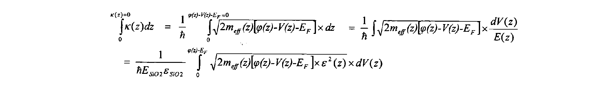
- Thus,

- It is believed that the above-described calculation procedure is useful for predicting the behavior of dielectric layers, gate stacks, and/or memory devices described herein; however, this calculation procedure should not be used to limit the scope of the present invention.
- A memory device may have any number of memory cells. In a conventional single-bit memory cell, a memory cell assumes one of two information storage states, either an "on" state or an "off" state. The binary condition of "on" or "off' defines one bit of information. As a result, a conventional memory device capable of storing n-bits of data requires (n) separate memory cells.
- The number of bits that can be stored using single-bit per cell memory devices depends upon the number of memory cells. Thus, increasing memory capacity requires larger die sizes containing more memory cells, or using improved photolithography techniques to create smaller memory cells. Smaller memory cells allow more memory cells to be placed within a given area of a single die.
- An alternative to a single-bit memory cell is a multi-bit or multistate memory cell, which can store more than one bit of data. A multi-bit or multistate flash memory cell may be produced by creating a memory cell with multiple, distinct threshold voltage levels, Vt1-n, as described, for example, in
U.S. Patent No. 5,583,812 , which is incorporated by reference herein in its entirety. Each distinct threshold voltage level, Vt1-n, corresponds to a value of a set of data bits, with the number of bits representing the amount of data that can be stored in the multistate memory cell. Thus, multiple bits of binary data can be stored within the same memory cell. - Each binary data value that can be stored in a multistate memory cell corresponds to a threshold voltage value or range of values over which the multistate memory cell conducts current. The multiple threshold voltage levels of a multistate memory cell are separated from each other by a sufficient amount so that a level of a multistate memory cell can be programmed or erased in an unambiguous manner. The specific relationship between the data programmed into the memory cell and the threshold voltage levels of the cell depends upon the data encoding scheme adopted for the multistate memory cell.
- In programming a multistate memory cell, a programming voltage is applied over a sufficient time period to store enough charge in the charge storage layer to move the multistate memory cell's threshold voltage to a desired level. This level represents a state of the multistate memory cell, corresponding to an encoding of the data programmed into the multistate memory cell.
- According to various exemplary embodiments, multiple threshold voltage levels for a multistate memory cell/device may be provided in
charge storage layer 204 by electrically isolated nanoparticles (such as shown inFIG. 8 ) or a contiguous or non-contiguous metal (or silicon) layer such as shown inFIG. 7 . - In another embodiment of multi-bit memory cells, as described for example in
U.S. Patent No. 5,768,192 , which is incorporated by reference herein in its entirety, charge is stored in a non-conductive charge trapping layer (e.g., a nitride layer) in two physically distinct regions on opposite sides of the memory cell near the source and drain regions of the device. By developing symmetric and interchangeable source and drain regions in the cell, two non-interactive physically distinct charge storage regions are created, with each region physically representing one bit of information mapped directly to the memory array and each cell thereby containing two bits of information. Programming of the cell is performed in a forward direction which includes injecting electrical charge into the charge trapping material within the gate utilizing hot electron injection for a sufficient time duration such that electrical charge becomes trapped asymmetrically in the charge trapping material, the electrical charge being injected until the threshold voltage of the gate reaches a predetermined level. The cell is then read in the reverse direction from which it was programmed. This type of multi-bit memory cell can also be extended to charge storage layer memory devices using discrete metal nanocrystals as the charge storage medium, as described, for example, inU.S. Appl. Pub. No. 2004/0130941 , which is incorporated by reference herein in its entirety. - The present inventors have also discovered that multi-bit storage using asymmetrical charge storage as described above can be accomplished using colloidal metal nanocrystals (e.g., as described in
U.S. Patent No. 6,586,785 and inU.S. Appl. Nos. 11/147,670 and11/495,188 - A significant feature of the use of the devices and methods described herein is that they may enable the reliable storage of multiple bits in a single device using, e.g., any of the conventional techniques for generating multi-state memory as described herein. Conventional flash memories using multi-bit storage achieved through the above-described methods such as the multi-level approach suffer from the stringent requirements on the control of the threshold spread. The present exemplary embodiments, however, may overcome many of the limitations of conventional flash memory devices by providing a large programming/erase window (on the order of, e.g., 8 volts or greater, or 12 volts or greater), increased programming/erasing speed and good charge retention. This may allow for a greater separation between the various threshold voltage states from each other so that a level of a multistate memory cell can be programmed or erased in an unambiguous manner.
- The present embodiments may also further enable the storage of multiple bits, such as three or more (e.g., four) bits per cell by, e.g., storing charge in each of two different storage locations in the charge storage layer and further adding the ability to store different quantities or charge states in each of the two locations using e.g., multiple voltage threshold levels as described above. The charge storage layer may be, for example, a nanocrystal layer or a non-conductive nitride layer, as described above. By storing four different quantities of charge at each location the memory device can thereby store 4x4=16 different combinations of charge providing the equivalent of four bits per cell. The enhancement in program/erase window provided by the teachings described herein without compromising charge retention may further enable multi-bit storage capability by providing greater flexibility in the injection and detection of charge in the storage medium and a relaxed requirement on threshold spread.
- The exemplary embodiments described herein may be assembled according to well known semiconductor manufacturing techniques.
FIG. 20 shows aflowchart 2000 providing an exemplary procedure for forming an electronic device, such as a memory device.Flowchart 2000 is provided for illustrative purposes, but is not intended to be limiting. Further structural and operational embodiments will be apparent to persons skilled in the relevant art(s) based on the following discussion. The procedure offlowchart 2000 does not necessarily have to be followed in the order shown. -
Flowchart 2000 begins with formation of a source region in asubstrate 2002. For example, as shown inFIG. 1 ,source region 112 may be formed insubstrate 102.Source region 112 may be formed according to conventional doping or other techniques. Furthermore, in an exemplary embodiment,source contact 104 may be formed onsource region 112 according to conventional deposition or other techniques. - Next, a drain region may be formed in the
substrate 2004. For example, as shown inFIG. 1 , drainregion 116 may be formed insubstrate 102.Drain region 116 may be formed according to conventional doping or other techniques. Furthermore, in an embodiment,drain contact 106 may be formed ondrain region 116 according to conventional deposition or other techniques. - A tunneling dielectric layer may be formed on the
substrate 2006. For example, as shown inFIGS. 2 and6 , tunnelingdielectric layer 202 may be formed onchannel region 114 ofsubstrate 102. Tunnelingdielectric layer 202 may be formed according to conventional oxide growth or other techniques. - A charge storage layer may be formed on the
tunneling dielectric layer 2008. For example, as shown inFIGS. 2 and6 ,charge storage layer 204 may be formed overtunneling dielectric layer 202. In an exemplary embodiment,charge storage layer 204 is formed directly on tunnelingdielectric layer 202. In another embodiment,charge storage layer 204 is formed on an intermediate layer formed on tunnelingdielectric layer 202, such asbarrier layer 302 shown inFIG. 3 . -
Charge storage layer 204 may be a metal or semiconductor material layer (continuous or non-continuous) or a layer of particles, such as further described above.Charge storage layer 204 may be formed by deposition techniques such as physical vapor deposition (PVD), chemical vapor deposition (CVD), electrochemical deposition (ECD), molecular beam epitaxy (MBE), atomic layer deposition (ALD), or other techniques described elsewhere herein or otherwise known. - The charge blocking layer may be formed on the
charge storage layer 2010. For example, as shown inFIGS. 2 and6 ,charge blocking layer 206 is formed overcharge storage layer 204.Charge blocking layer 206 may be formed according to any deposition technique described elsewhere herein or otherwise known, such as by atomic layer deposition. In an exemplary embodiment, as described above,charge blocking layer 206 may be doped. Furthermore, in another exemplary embodiment, as described above,charge blocking layer 206 may be formed as a gradient or as having multiple layers. - Atomic layer deposition may be particularly suitable for forming a
charge blocking layer 206 including a composition gradient or multiple layers. For example, to form acharge blocking layer 206 composed of a dielectric material having a component that varies in concentration across a thickness of thecharge blocking layer 206, one or more first monolayers of the dielectric material may be deposited using a first precursor of a first chemistry, and then one or more second monolayers of the dielectric material may be deposited using a second precursor of a second chemistry, and then one or more third monolayers of the dielectric material may be deposited using a third precursor of a third chemistry, etc. In other words, consecutive depositions of one or more monolayers may be carried out using different precursors in order to form thecharge blocking layer 206 including either a composition gradient or multiple layers. It is also envisioned that acharge blocking layer 206 of a uniform composition may be deposited initially and then a rapid thermal anneal (RTA) may be employed to achieve the effect of a compositionally graded layer. - A control dielectric layer may be formed on the
charge blocking layer 2012. For example, as shown inFIGS. 2 and6 , controldielectric layer 208 is formed overcharge blocking layer 206.Control dielectric layer 208 may be formed according to any deposition technique described elsewhere herein or otherwise known, such as by atomic layer deposition. - A second charge blocking layer may be formed over the
control dielectric layer 2014. As shown inFIG. 6 , secondcharge blocking layer 402 is formed over controldielectric layer 208. Secondcharge blocking layer 402 may be formed according to any deposition technique described elsewhere herein or otherwise known, such as atomic layer deposition. In an embodiment, in a similar fashion to firstcharge blocking layer 206, secondcharge blocking layer 402 may be doped. Furthermore, in an embodiment, in a similar fashion to firstcharge blocking layer 206, secondcharge blocking layer 402 may be formed as a gradient or as having multiple layers. - The second
charge blocking layer 402 is not necessarily formed in all embodiments. For example,FIG. 2 shows agate stack 120 that does not include a second charge blocking layer. In another example, as shown inFIG. 11 , thegate stack 120 may include thecharge blocking layer 206 on thecontrol dielectric layer 208, and a second charge blocking layer may not be formed. - A control gate may be formed over the
gate stack 2016. For example, as shown inFIG. 2 ,gate contact 118 is formed over controldielectric layer 208 ofgate stack 120. As shown inFIG. 6 ,gate contact 118 is formed over secondcharge blocking layer 402 ofgate stack 120".Gate contact 118 may be formed ongate stacks - Methods, systems and apparatuses for improved electronic devices, such as memory devices that may have enhanced characteristics, including increased charge retention, enhanced memory program/erase window, improved reliability and stability, with feasibility for single or multistate (e.g., two, three or four bit) operation, have been described herein.
- The use of a multi-layer control dielectric, such as a double or triple layer control dielectric, in a nonvolatile memory device has been disclosed. The multi-layer control dielectric may include a combination of high-k dielectric materials such as aluminum oxide (Al2O3), hafnium oxide (HfO2), and/or hybrid films of hafnium aluminum oxide (HfAlOx, wherein x is a positive integer, e.g., 1, 2, 3, 4, etc.) therein.
- A double control dielectric layer for a memory device has been described, including, for example, a control dielectric layer of Al2O3, and a charge blocking layer of HfO2 (or Hf1-xAlxOy, where x is a positive number between 0 and 1, and y is a positive number, e.g., HfAlO3). The layer of HfO2 may provide an efficient charge blocking layer to block electron current flow from the charge storage layer to the control gate during a programming operation of the memory device.
- A double control dielectric layer for a memory device including, for example, a control dielectric layer of Al2O3 and a layer of a hafnium containing compound such as HfO2 between the control dielectric and the control gate has also been disclosed. The layer of HfO2 may suppress a tunneling current from a control gate of the memory device during erase operations which can lead to large over-erase voltages.
- A double control dielectric layer for a memory device including, for example, a control dielectric layer of Al2O3 and a layer of a hafnium containing compound such as HfO2 between the control dielectric and the charge storage layer has also been disclosed. The layer of HfO2 may suppress a tunneling current from the charge storage layer of the memory device to the control gate during programming operations.
- A triple control dielectric layer for a memory device also has been described. For example, the triple control dielectric layer may include a first layer of a hafnium containing compound such as HfO2 (or Hf1-xAlxOy, where x is a positive number between 0 and 1, and y is a positive number, e.g., HfAlO3) adjacent to the charge storage layer of the device, a second layer of a hafnium containing compound such as HfO2 adjacent to the control gate of the memory device, and a layer of Al2O3 between the first and second layers of HfO2. The second layer of HfO2 may block electron current from the control gate to the charge storage layer during the erase operation of the memory device.
- The thickness of single or dual layers of the charge blocking layer may be kept very thin while still efficiently blocking current flow. For example, in an embodiment, the thickness is less than about 10 nm e.g., less than about 5 nm, e.g., less than about 4 nm. In another example embodiment, the thickness is less than about 2 nm. Preferably, the thickness is greater than about 0.1 nm
- The use of such a double or triple layer control dielectric may provide the unexpected result of achieving a very large program/erase window (e.g., on the order of at least 8 volts or greater, for example, about 9 volts, e.g., about 10 volts, e.g., about 11 volts, e.g., about 12 volts or greater), while still providing for good charge retention and programming/erasing speed, which is important in making reliable multi-bit/cell memory devices with scaling to smaller node sizes. Furthermore, the charge blocking layer may dramatically reduce the amount of current that flows through the control dielectric during the program, erase, and read operations, which may enable flash memory devices that can endure a large number of program/erase cycles without significant drift in operation voltages.
- In exemplary embodiments, various high-k dielectric materials, such as Gd2O3, Yb2O3, Dy2O3, Nb2O5, Y2O3, La2O3, ZrO2, TiO2, Ta2O5, SrTiO3, BaxSr1-xTiO3, ZrxSi1-xOy, HfxSi1-xOy, HfxSi1-xO2-yNy, AlxZr1-xO2, or Pr2O, for example, may be used for the charge blocking layer.
- A charge blocking layer including a composition gradient across the thickness of the charge blocking layer also has been described herein. For example, the charge blocking layer may be made of a dielectric material, and an amount of at least one component of the dielectric material may vary across the thickness of the charge blocking layer. For example, the component may be hafnium or hafnium oxide. According to an exemplary embodiment, the charge blocking layer having a composition gradient may be formed of a multicomponent oxide such as, for example, HfxAl1-xOy, HfxSi1-xOy, ZrxSi1-xOy, BaxSr1-xTiOy, and AlxZr1-xOy. The multicomponent oxide may include nitrogen (e.g., HfxSi1-xO2-yNy) according to an exemplary embodiment. The charge blocking layer having a composition gradient may be disposed between the charge storage layer and the control dielectric layer, or between the control dielectric layer and the gate contact of the memory device. According to some exemplary embodiments, the gate stack may include both a first and a second charge blocking layer. One or both charge blocking layers may have a composition gradient, as described herein.
- While various embodiments of the present invention have been described above, it should be understood that they have been presented by way of example only, and not limitation. It will be apparent to persons skilled in the relevant art that various changes in form and detail can be made therein without departing from the spirit and scope of the invention. Thus, the breadth and scope of the present invention should not be limited by any of the above-described exemplary embodiments, but should be defined only in accordance with the following claims and their equivalents.
Claims (47)
- A gate stack of a memory device, the gate stack comprising:a charge storage layer on a dielectric layer;a first dielectric layer on the charge storage layer;a second dielectric layer comprising a high-k dielectric material on the first dielectric layer.
- The gate stack of claim 1, wherein the charge storage layer comprises a localized charge storage layer.
- The gate stack of claim 2, wherein the localized charge storage layer comprises a plurality of nanocrystals.
- The gate stack of claim 2, wherein the localized charge storage layer comprises a nitride layer.
- The gate stack of claim 1, wherein the second dielectric layer comprises a dielectric constant higher than a dielectric constant of the first dielectric layer..
- The gate stack of claim 5, wherein the first dielectric layer has a thickness of about 15 nm or less and the second dielectric layer has a thickness of about 10 nm or less.
- The gate stack of claim 1, wherein the second dielectric layer comprises hafnium.
- The gate stack of claim 7, wherein the second dielectric layer comprises a hafnium-containing compound selected from the group consisting of: HfO2, HfAlO3, HfSiO2, Hf1-xAlxOy, Hf1-xSixOy, Hf1-xSixO2-yNy, where x is a positive number between 0 and 1, and y is a positive number.
- The gate stack of claim 1, wherein the first dielectric layer comprises Al2O3 and the second dielectric layer comprises HfO2.
- The gate stack of claim 1, wherein the first dielectric layer comprises SiO2 and the second dielectric layer comprises HfO2.
- The gate stack of claim 1, wherein an amount of at least a first component of a dielectric material of the second dielectric layer varies in a predetermined manner across a thickness thereof.
- The gate stack of claim 11, wherein the dielectric material includes the first component and a second component, and a ratio of the first component to the second component varies in a predetermined manner across the thickness of the second dielectric layer.
- The gate stack of claim 1, wherein the second dielectric layer comprises a plurality of layers.
- The gate stack of claim 1, further comprising a third dielectric layer adjacent to the first dielectric layer, the first dielectric layer being disposed between the second and third dielectric layers.
- The gate stack of claim 14, wherein a dielectric constant of the third dielectric layer is greater than a dielectric constant of the first dielectric layer.
- The gate stack of claim 14, wherein the third dielectric layer is disposed between the first dielectric layer and the charge storage layer.
- The gate stack of claim 16, wherein the third dielectric layer comprises hafnium.
- The gate stack of claim 17, wherein the third dielectric layer comprises a hafnium-containing compound selected from the group consisting of: HfO2, HfAlO3, HfSiO2, Hf1-xAlxOy, Hf1-xSixOy, Hf1-xSixO2-yNy, where x is a positive number between 0 and 1, and y is a positive number.
- The gate stack of claim 16, wherein the charge storage layer comprises a plurality of nanocrystals.
- The gate stack of claim 16, wherein the memory device has a program/erase window of greater than about 8 volts.
- The gate stack of claim 20, wherein the memory device has a program/erase window of greater than about 9 volts.
- The gate stack of claim 21, wherein the memory device has a program/erase window of greater than about 10 volts.
- The gate stack of claim 16, wherein the first dielectric layer comprises Al2O3 and the second and third dielectric layers comprise HfO2.
- The gate stack of claim 16, wherein the first dielectric layer comprises SiO2 and the second and third dielectric layers comprise HfO2.
- The gate stack of claim 1, wherein the second dielectric layer is disposed between the first dielectric layer and a gate contact of the memory device.
- The gate stack of claim 1, wherein a thickness of the first dielectric layer is no more than about 200% of a thickness of the second dielectric layer.
- The gate stack of claim 1, wherein a tunneling current through the first dielectric layer is less than about 10-4 A/cm2 at an electric field strength that is equivalent to an electric field strength of 2.5 x 10⁷ V/cm in SiO2.
- The gate stack of claim 1, further comprising a gate contact on the second dielectric layer, wherein the gate contact comprises a metal.
- A gate stack of a memory device, the gate stack comprising:a charge storage layer between a tunneling dielectric layer and a control dielectric layer; anda charge blocking layer adjacent to the control dielectric layer, the charge blocking layer comprising a hafnium-containing compound.
- A gate stack of a memory device, the gate stack comprising:a charge storage layer between a tunneling dielectric layer and a control dielectric layer; anda dielectric layer comprising a dielectric material adjacent to the control dielectric layer,wherein an amount of at least a first component of the dielectric material varies in a predetermined manner across a thickness of the dielectric layer.
- A gate stack of a memory device, the gate stack comprising:a charge storage layer between a tunneling dielectric layer and a control dielectric layer having a thickness of about 5 nm or less; anda charge blocking layer adjacent to the control dielectric layer, the charge blocking layer comprising a dielectric material.
- A gate stack of a memory device, the gate stack comprising:a charge storage layer between a tunneling dielectric layer and a control dielectric layer;a charge blocking layer adjacent to the control dielectric layer, the charge blocking layer comprising a dielectric material,wherein a thickness of the control dielectric layer is no more than about 200% of a thickness of the charge blocking layer.
- A memory device comprising:a substrate comprising a source region, a drain region, and a channel region between the source region and the drain region;a gate stack on the substrate adjacent to a control gate, the gate stack comprising:a first dielectric layer adjacent to the control gate;a charge storage layer between the first dielectric layer and a tunneling dielectric layer; anda second dielectric layer comprising a dielectric material adjacent to the first dielectric layer, wherein an amount of at least a first component of the dielectric material varies in a predetermined manner across a thickness of the second dielectric layer.
- A gate stack of a memory device comprising:a charge storage layer between a tunneling dielectric layer and a control dielectric layer, the control dielectric layer comprising SiO2; anda high-k dielectric layer comprising a high-k dielectric material adjacent to the control dielectric layer.
- A gate stack of a memory device comprising:a tunneling dielectric layer;a charge storage layer above the tunneling dielectric layer;a first dielectric layer adjacent the charge storage layer comprising a first dielectric material having a first dielectric constant;a second dielectric layer adjacent the first dielectric layer comprising a second dielectric material having a second dielectric constant; anda third dielectric layer adjacent the second dielectric layer comprising a third dielectric material having a third dielectric constant,wherein the first and third dielectric constants are greater than the second dielectric constant.
- A method of making a gate stack for a memory device, the method comprising:forming a charge storage layer on a tunneling dielectric layer;forming a control dielectric layer on the charge storage layer;forming a charge blocking layer comprising a dielectric material on the control dielectric layer and varying an amount of at least a first component of the dielectric material across a thickness of the charge blocking layer.
- A memory device, comprising:a substrate;a source region of the substrate;a drain region of the substrate;a channel region between the source region and drain region;a tunneling dielectric layer on the channel region;a nitride layer on the tunneling dielectric layer;a control dielectric layer on the nitride layer;a charge blocking layer on the control dielectric layer; anda control gate on the charge blocking layer.
- A gate stack of a memory device, comprising:a tunneling dielectric layer;a nitride layer on the tunneling dielectric layer;a control dielectric layer on the nitride layer; anda charge blocking layer on the control dielectric layer.
- A method for forming a memory device, comprising:forming a tunneling dielectric layer on a substrate;forming a nitride layer on the tunneling dielectric layer;forming a control dielectric layer on the nitride layer;forming a charge blocking layer on the control dielectric layer; andforming a control gate on the charge blocking layer.
- A memory cell of a flash memory device, the memory cell comprising:a charge storage layer;a first dielectric layer adjacent to the charge storage layer; anda second dielectric layer adjacent to the first dielectric layer;wherein the memory cell has a program/erase window of greater than about 8 volts.
- A memory device comprising:a substrate comprising a source region, a drain region, and a channel region between the source region and the drain region;a gate stack on the substrate adjacent to a control gate, the gate stack comprising:a charge blocking layer between the control gate and a control dielectric layer; anda charge storage layer between the control dielectric layer and a tunneling dielectric layer.
- A memory device comprising:a substrate comprising a source region, a drain region, and a channel region between the source region and the drain region;a gate stack on the substrate adjacent to a control gate, the gate stack comprising:a layer comprising a hafnium-containing compound between the control gate and a dielectric layer;a nitride layer between the dielectric layer and a second dielectric layer.
- A gate stack of a memory device, the gate stack comprising:a nitride layer between a tunneling dielectric layer and a control dielectric layer;a charge blocking layer adjacent to the control dielectric layer.
- A gate stack for a multi-bit memory cell, the gate stack comprising:a nitride layer between a tunneling dielectric layer and a control dielectric layer;a charge blocking layer adjacent to the control dielectric layer,wherein charge is stored in the nitride layer in at least two physically distinct charge storage regions.
- A memory device, comprising:a substrate;a source region of the substrate;a drain region of the substrate;a channel region between the source region and drain region;a tunneling dielectric layer over the substrate adjacent to the channel region;a charge storage layer over the tunneling dielectric layer;a charge blocking layer over the charge storage layer;a control dielectric layer over the charge blocking layer; anda control gate over the control dielectric layer.
- A gate stack of a memory device, comprising:a tunneling dielectric layer over a substrate of the memory device;a charge storage layer over the tunneling dielectric layer;a charge blocking layer over the charge storage layer; anda control dielectric layer over the charge blocking layer;wherein a control gate is over the control dielectric layer.
- A method for forming a memory device, comprising:forming a tunneling dielectric layer over a substrate;forming a charge storage layer over the tunneling dielectric layer;forming a charge blocking layer over the charge storage layer;forming a control dielectric layer over the charge blocking layer; andforming a control gate over the control dielectric layer.
Priority Applications (6)
| Application Number | Priority Date | Filing Date | Title |
|---|---|---|---|
| EP11155070A EP2357662A3 (en) | 2006-12-20 | 2007-06-14 | Electron blocking layers for gate stacks of nonvolatile memory devices |
| PCT/US2007/087167 WO2008079684A2 (en) | 2006-12-20 | 2007-12-12 | Electron blocking layers for electronic devices |
| CN200780046789.2A CN101589461B (en) | 2006-12-20 | 2007-12-12 | Electron blocking layers for electronic devices |
| JP2009543077A JP2010531048A (en) | 2006-12-20 | 2007-12-12 | Electronic block layer for electronic devices |
| KR1020097012821A KR101443731B1 (en) | 2006-12-20 | 2007-12-12 | Electron blocking layers for electronic devices |
| TW96149083A TWI361494B (en) | 2006-12-20 | 2007-12-20 | Electron blocking layers for electronic devices |
Applications Claiming Priority (3)
| Application Number | Priority Date | Filing Date | Title |
|---|---|---|---|
| US11/641,956 US20080150003A1 (en) | 2006-12-20 | 2006-12-20 | Electron blocking layers for electronic devices |
| US11/688,087 US20080150004A1 (en) | 2006-12-20 | 2007-03-19 | Electron Blocking Layers for Electronic Devices |
| US11/743,085 US20080150009A1 (en) | 2006-12-20 | 2007-05-01 | Electron Blocking Layers for Electronic Devices |
Publications (1)
| Publication Number | Publication Date |
|---|---|
| EP1936672A1 true EP1936672A1 (en) | 2008-06-25 |
Family
ID=39541587
Family Applications (2)
| Application Number | Title | Priority Date | Filing Date |
|---|---|---|---|
| EP07252410A Ceased EP1936672A1 (en) | 2006-12-20 | 2007-06-14 | Electron blocking layers for gate stacks of nonvolatile memory devices |
| EP11155070A Withdrawn EP2357662A3 (en) | 2006-12-20 | 2007-06-14 | Electron blocking layers for gate stacks of nonvolatile memory devices |
Family Applications After (1)
| Application Number | Title | Priority Date | Filing Date |
|---|---|---|---|
| EP11155070A Withdrawn EP2357662A3 (en) | 2006-12-20 | 2007-06-14 | Electron blocking layers for gate stacks of nonvolatile memory devices |
Country Status (3)
| Country | Link |
|---|---|
| US (1) | US20080150009A1 (en) |
| EP (2) | EP1936672A1 (en) |
| JP (1) | JP2010531048A (en) |
Cited By (2)
| Publication number | Priority date | Publication date | Assignee | Title |
|---|---|---|---|---|
| CN102610653A (en) * | 2011-01-20 | 2012-07-25 | 中国科学院微电子研究所 | Nanocrystalline floating gate memory and manufacturing method of nanocrystalline floating gate memory |
| CN110349963A (en) * | 2013-02-26 | 2019-10-18 | 经度快闪存储解决方案有限责任公司 | The storage unit based on SONOS of insertion |
Families Citing this family (19)
| Publication number | Priority date | Publication date | Assignee | Title |
|---|---|---|---|---|
| US7454295B2 (en) | 1998-12-17 | 2008-11-18 | The Watereye Corporation | Anti-terrorism water quality monitoring system |
| US9056783B2 (en) | 1998-12-17 | 2015-06-16 | Hach Company | System for monitoring discharges into a waste water collection system |
| US8958917B2 (en) | 1998-12-17 | 2015-02-17 | Hach Company | Method and system for remote monitoring of fluid quality and treatment |
| US8920619B2 (en) | 2003-03-19 | 2014-12-30 | Hach Company | Carbon nanotube sensor |
| US7968273B2 (en) | 2004-06-08 | 2011-06-28 | Nanosys, Inc. | Methods and devices for forming nanostructure monolayers and devices including such monolayers |
| US7776758B2 (en) | 2004-06-08 | 2010-08-17 | Nanosys, Inc. | Methods and devices for forming nanostructure monolayers and devices including such monolayers |
| US7847341B2 (en) * | 2006-12-20 | 2010-12-07 | Nanosys, Inc. | Electron blocking layers for electronic devices |
| US8686490B2 (en) * | 2006-12-20 | 2014-04-01 | Sandisk Corporation | Electron blocking layers for electronic devices |
| US20080150003A1 (en) * | 2006-12-20 | 2008-06-26 | Jian Chen | Electron blocking layers for electronic devices |
| CN101755338B (en) * | 2007-07-18 | 2012-10-10 | 松下电器产业株式会社 | Current limiting element, memory device using current limiting element |
| US7816727B2 (en) * | 2007-08-27 | 2010-10-19 | Macronix International Co., Ltd. | High-κ capped blocking dielectric bandgap engineered SONOS and MONOS |
| JP2010021204A (en) * | 2008-07-08 | 2010-01-28 | Toshiba Corp | Semiconductor device and manufacturing method thereof |
| US8313994B2 (en) * | 2009-03-26 | 2012-11-20 | Tokyo Electron Limited | Method for forming a high-K gate stack with reduced effective oxide thickness |
| KR101094554B1 (en) * | 2009-06-08 | 2011-12-19 | 주식회사 하이닉스반도체 | Method of manufacturing nonvolatile memory device |
| US8383479B2 (en) * | 2009-07-21 | 2013-02-26 | Sandisk Technologies Inc. | Integrated nanostructure-based non-volatile memory fabrication |
| US8298890B1 (en) | 2009-09-03 | 2012-10-30 | Intermolecular, Inc. | Charge blocking layers for nonvolatile memories |
| US8288811B2 (en) * | 2010-03-22 | 2012-10-16 | Micron Technology, Inc. | Fortification of charge-storing material in high-K dielectric environments and resulting apparatuses |
| JP5613105B2 (en) | 2011-05-27 | 2014-10-22 | 株式会社東芝 | Nonvolatile semiconductor memory device and manufacturing method thereof |
| JP7089967B2 (en) * | 2018-07-17 | 2022-06-23 | ルネサスエレクトロニクス株式会社 | Semiconductor devices and their manufacturing methods |
Citations (11)
| Publication number | Priority date | Publication date | Assignee | Title |
|---|---|---|---|---|
| US5583812A (en) | 1988-06-08 | 1996-12-10 | Harari; Eliyahou | Flash EEPROM system cell array with more than two storage states per memory cell |
| US5768192A (en) | 1996-07-23 | 1998-06-16 | Saifun Semiconductors, Ltd. | Non-volatile semiconductor memory cell utilizing asymmetrical charge trapping |
| US6297095B1 (en) | 2000-06-16 | 2001-10-02 | Motorola, Inc. | Memory device that includes passivated nanoclusters and method for manufacture |
| US6586785B2 (en) | 2000-06-29 | 2003-07-01 | California Institute Of Technology | Aerosol silicon nanoparticles for use in semiconductor device fabrication |
| EP1324378A1 (en) * | 2001-12-31 | 2003-07-02 | Memscap | Mehrlagige Struktur, verwendet für Materialine mit hoher Permitivität |
| US6642573B1 (en) | 2002-03-13 | 2003-11-04 | Advanced Micro Devices, Inc. | Use of high-K dielectric material in modified ONO structure for semiconductor devices |
| US20040130941A1 (en) | 2002-11-26 | 2004-07-08 | Cornell Research Foundation, Inc. | Multibit metal nanocrystal memories and fabrication |
| US20050093054A1 (en) * | 2003-11-05 | 2005-05-05 | Jung Jin H. | Non-volatile memory devices and methods of fabricating the same |
| US20050280069A1 (en) * | 2004-06-21 | 2005-12-22 | Ichiro Mizushima | Semiconductor device and method of manufacturing the same |
| US20060175656A1 (en) * | 2001-04-27 | 2006-08-10 | Interuniversitair Microelektronica Centrum (Imec Vzw) | Non-volatile memory devices |
| US20060180851A1 (en) | 2001-06-28 | 2006-08-17 | Samsung Electronics Co., Ltd. | Non-volatile memory devices and methods of operating the same |
Family Cites Families (86)
| Publication number | Priority date | Publication date | Assignee | Title |
|---|---|---|---|---|
| US6005A (en) * | 1849-01-09 | Machine for hook-heading spikes by one motion | ||
| US6018A (en) * | 1849-01-09 | Improvement in bog-cutters | ||
| US5043940A (en) * | 1988-06-08 | 1991-08-27 | Eliyahou Harari | Flash EEPROM memory systems having multistate storage cells |
| US5172338B1 (en) * | 1989-04-13 | 1997-07-08 | Sandisk Corp | Multi-state eeprom read and write circuits and techniques |
| DE69034191T2 (en) * | 1989-04-13 | 2005-11-24 | Sandisk Corp., Sunnyvale | EEPROM system with multi-chip block erasure |
| US6222762B1 (en) * | 1992-01-14 | 2001-04-24 | Sandisk Corporation | Multi-state memory |
| US5714766A (en) * | 1995-09-29 | 1998-02-03 | International Business Machines Corporation | Nano-structure memory device |
| US5890192A (en) * | 1996-11-05 | 1999-03-30 | Sandisk Corporation | Concurrent write of multiple chunks of data into multiple subarrays of flash EEPROM |
| US5740104A (en) * | 1997-01-29 | 1998-04-14 | Micron Technology, Inc. | Multi-state flash memory cell and method for programming single electron differences |
| US6159620A (en) * | 1997-03-31 | 2000-12-12 | The Regents Of The University Of California | Single-electron solid state electronic device |
| FR2762931B1 (en) * | 1997-05-05 | 1999-06-11 | Commissariat Energie Atomique | QUANTUM ISLANDS DEVICE AND MANUFACTURING METHOD |
| US20030077625A1 (en) * | 1997-05-27 | 2003-04-24 | Hutchison James E. | Particles by facile ligand exchange reactions |
| US6054349A (en) * | 1997-06-12 | 2000-04-25 | Fujitsu Limited | Single-electron device including therein nanocrystals |
| JP3727449B2 (en) * | 1997-09-30 | 2005-12-14 | シャープ株式会社 | Method for producing semiconductor nanocrystal |
| US6322901B1 (en) * | 1997-11-13 | 2001-11-27 | Massachusetts Institute Of Technology | Highly luminescent color-selective nano-crystalline materials |
| US6232643B1 (en) * | 1997-11-13 | 2001-05-15 | Micron Technology, Inc. | Memory using insulator traps |
| US6060895A (en) * | 1998-04-20 | 2000-05-09 | Fairchild Semiconductor Corp. | Wafer level dielectric test structure and related method for accelerated endurance testing |
| KR100294691B1 (en) * | 1998-06-29 | 2001-07-12 | 김영환 | Memory device using multilevel quantum dot structure and method of the same |
| US6139626A (en) * | 1998-09-04 | 2000-10-31 | Nec Research Institute, Inc. | Three-dimensionally patterned materials and methods for manufacturing same using nanocrystals |
| US6477532B1 (en) * | 1999-06-30 | 2002-11-05 | Net4Music S.A. | Process for the remote publishing of musical scores |
| DE60044972D1 (en) * | 1999-07-02 | 2010-10-28 | Harvard College | NANOSCOPIC WIRE CONTAINING ARRANGEMENT, LOGISC |
| US6319775B1 (en) * | 1999-10-25 | 2001-11-20 | Advanced Micro Devices, Inc. | Nitridation process for fabricating an ONO floating-gate electrode in a two-bit EEPROM device |
| US6407435B1 (en) * | 2000-02-11 | 2002-06-18 | Sharp Laboratories Of America, Inc. | Multilayer dielectric stack and method |
| AU2001249459A1 (en) * | 2000-03-24 | 2001-10-08 | The State Of Oregon, Acting By And Through The State Board Of Higher Education On Behalf Of The University Of Oregon | Scaffold-organized clusters and electronic devices made using such clusters |
| US6413819B1 (en) * | 2000-06-16 | 2002-07-02 | Motorola, Inc. | Memory device and method for using prefabricated isolated storage elements |
| US6344403B1 (en) * | 2000-06-16 | 2002-02-05 | Motorola, Inc. | Memory device and method for manufacture |
| TWI292583B (en) * | 2000-08-22 | 2008-01-11 | Harvard College | Doped elongated semiconductor articles, growing such articles, devices including such articles and fabicating such devices |
| US6610615B1 (en) * | 2000-11-15 | 2003-08-26 | Intel Corporation | Plasma nitridation for reduced leakage gate dielectric layers |
| US6576291B2 (en) * | 2000-12-08 | 2003-06-10 | Massachusetts Institute Of Technology | Preparation of nanocrystallites |
| AU2002229046B2 (en) * | 2000-12-11 | 2006-05-18 | President And Fellows Of Harvard College | Nanosensors |
| US6602805B2 (en) * | 2000-12-14 | 2003-08-05 | Macronix International Co., Ltd. | Method for forming gate dielectric layer in NROM |
| US6942740B2 (en) * | 2001-01-19 | 2005-09-13 | Jfe Steel Corporation | Grain-oriented magnetic steel sheet having no undercoat film comprising forsterite as primary component and having good magnetic characteristics |
| JP2002217318A (en) * | 2001-01-19 | 2002-08-02 | Sony Corp | Non-volatile semiconductor storage element and its manufacturing method |
| US6713846B1 (en) * | 2001-01-26 | 2004-03-30 | Aviza Technology, Inc. | Multilayer high κ dielectric films |
| US6844604B2 (en) * | 2001-02-02 | 2005-01-18 | Samsung Electronics Co., Ltd. | Dielectric layer for semiconductor device and method of manufacturing the same |
| KR100408520B1 (en) * | 2001-05-10 | 2003-12-06 | 삼성전자주식회사 | Single electron memory device comprising quantum dots between gate electrode and single electron storage element and method for manufacturing the same |
| US6891231B2 (en) * | 2001-06-13 | 2005-05-10 | International Business Machines Corporation | Complementary metal oxide semiconductor (CMOS) gate stack with high dielectric constant gate dielectric and integrated diffusion barrier |
| US6562491B1 (en) * | 2001-10-15 | 2003-05-13 | Advanced Micro Devices, Inc. | Preparation of composite high-K dielectrics |
| US6559014B1 (en) * | 2001-10-15 | 2003-05-06 | Advanced Micro Devices, Inc. | Preparation of composite high-K / standard-K dielectrics for semiconductor devices |
| US6656792B2 (en) * | 2001-10-19 | 2003-12-02 | Chartered Semiconductor Manufacturing Ltd | Nanocrystal flash memory device and manufacturing method therefor |
| KR100459895B1 (en) * | 2002-02-09 | 2004-12-04 | 삼성전자주식회사 | Memory device with quantum dot and method of manufacturing the same |
| US6586349B1 (en) * | 2002-02-21 | 2003-07-01 | Advanced Micro Devices, Inc. | Integrated process for fabrication of graded composite dielectric material layers for semiconductor devices |
| US6717226B2 (en) * | 2002-03-15 | 2004-04-06 | Motorola, Inc. | Transistor with layered high-K gate dielectric and method therefor |
| US6872645B2 (en) * | 2002-04-02 | 2005-03-29 | Nanosys, Inc. | Methods of positioning and/or orienting nanostructures |
| US6750066B1 (en) * | 2002-04-08 | 2004-06-15 | Advanced Micro Devices, Inc. | Precision high-K intergate dielectric layer |
| US7005697B2 (en) * | 2002-06-21 | 2006-02-28 | Micron Technology, Inc. | Method of forming a non-volatile electron storage memory and the resulting device |
| US6996009B2 (en) * | 2002-06-21 | 2006-02-07 | Micron Technology, Inc. | NOR flash memory cell with high storage density |
| US6888739B2 (en) * | 2002-06-21 | 2005-05-03 | Micron Technology Inc. | Nanocrystal write once read only memory for archival storage |
| US7154140B2 (en) * | 2002-06-21 | 2006-12-26 | Micron Technology, Inc. | Write once read only memory with large work function floating gates |
| US7221586B2 (en) * | 2002-07-08 | 2007-05-22 | Micron Technology, Inc. | Memory utilizing oxide nanolaminates |
| US6753570B1 (en) * | 2002-08-20 | 2004-06-22 | Advanced Micro Devices, Inc. | Memory device and method of making |
| US20040144972A1 (en) * | 2002-10-04 | 2004-07-29 | Hongjie Dai | Carbon nanotube circuits with high-kappa dielectrics |
| US6753224B1 (en) * | 2002-12-19 | 2004-06-22 | Taiwan Semiconductor Manufacturing Company | Layer of high-k inter-poly dielectric |
| JP2004281662A (en) * | 2003-03-14 | 2004-10-07 | Toshiba Corp | Semiconductor memory device and its manufacturing method |
| JP4040534B2 (en) * | 2003-06-04 | 2008-01-30 | 株式会社東芝 | Semiconductor memory device |
| KR100703833B1 (en) * | 2003-06-30 | 2007-04-05 | 주식회사 하이닉스반도체 | Method for fabricating capacitor with double dielectric layer |
| US6951782B2 (en) * | 2003-07-30 | 2005-10-04 | Promos Technologies, Inc. | Nonvolatile memory cell with multiple floating gates formed after the select gate and having upward protrusions |
| AU2004265938B2 (en) * | 2003-08-04 | 2009-07-02 | Nanosys, Inc. | System and process for producing nanowire composites and electronic substrates therefrom |
| AU2004203889B2 (en) * | 2003-08-22 | 2006-02-23 | Panasonic Healthcare Holdings Co., Ltd. | ZrO2-Al2O3 composite ceramic material |
| KR100541551B1 (en) * | 2003-09-19 | 2006-01-10 | 삼성전자주식회사 | Analog capacitor having at least 3 layers of high-k dielectric layers and method of fabricating the same |
| EP2299482A3 (en) * | 2003-10-06 | 2014-12-17 | Massachusetts Institute Of Technology | Non-volatile memory device |
| KR100639673B1 (en) * | 2003-12-22 | 2006-10-30 | 삼성전자주식회사 | Semiconductor device including a gate dielectric layer formed of a high dielectric alloy and method of fabricating the same |
| US20050202615A1 (en) * | 2004-03-10 | 2005-09-15 | Nanosys, Inc. | Nano-enabled memory devices and anisotropic charge carrying arrays |
| US7595528B2 (en) * | 2004-03-10 | 2009-09-29 | Nanosys, Inc. | Nano-enabled memory devices and anisotropic charge carrying arrays |
| JP2005317647A (en) * | 2004-04-27 | 2005-11-10 | Toshiba Corp | Semiconductor device and its fabrication process |
| US7776758B2 (en) * | 2004-06-08 | 2010-08-17 | Nanosys, Inc. | Methods and devices for forming nanostructure monolayers and devices including such monolayers |
| TW201341440A (en) * | 2004-06-08 | 2013-10-16 | Sandisk Corp | Post-deposition encapsulation of nanostructures: compositions, devices and systems incorporating same |
| JP2006005006A (en) * | 2004-06-15 | 2006-01-05 | Toshiba Corp | Nonvolatile semiconductor memory |
| US7138680B2 (en) * | 2004-09-14 | 2006-11-21 | Infineon Technologies Ag | Memory device with floating gate stack |
| US7183180B2 (en) * | 2004-10-13 | 2007-02-27 | Atmel Corporation | Method for simultaneous fabrication of a nanocrystal and non-nanocrystal device |
| US7365389B1 (en) * | 2004-12-10 | 2008-04-29 | Spansion Llc | Memory cell having enhanced high-K dielectric |
| US7479425B2 (en) * | 2005-01-20 | 2009-01-20 | Chartered Semiconductor Manufacturing, Ltd | Method for forming high-K charge storage device |
| US7361567B2 (en) * | 2005-01-26 | 2008-04-22 | Freescale Semiconductor, Inc. | Non-volatile nanocrystal memory and method therefor |
| KR101078125B1 (en) * | 2005-02-07 | 2011-10-28 | 삼성전자주식회사 | Nonvolatile Nano-channel Memory Device using Mesoporous Material |
| JP2006229044A (en) * | 2005-02-18 | 2006-08-31 | Toshiba Corp | Semiconductor device |
| KR100652402B1 (en) * | 2005-02-21 | 2006-12-01 | 삼성전자주식회사 | Non-volatile memory device, and method of fabricating the same |
| US7217643B2 (en) * | 2005-02-24 | 2007-05-15 | Freescale Semiconductors, Inc. | Semiconductor structures and methods for fabricating semiconductor structures comprising high dielectric constant stacked structures |
| US20060231889A1 (en) * | 2005-04-13 | 2006-10-19 | Tupei Chen | Two-terminal solid-state memory device and two-terminal flexible memory device based on nanocrystals or nanoparticles |
| US20060275975A1 (en) * | 2005-06-01 | 2006-12-07 | Matt Yeh | Nitridated gate dielectric layer |
| WO2007024697A2 (en) * | 2005-08-19 | 2007-03-01 | Nanosys, Inc. | Electronic grade metal nanostructures |
| KR100648860B1 (en) * | 2005-09-08 | 2006-11-24 | 주식회사 하이닉스반도체 | Dielectric and method for forming the same, semiconductor memory device having the dielectric and method for manufacturing the semiconductor memory device |
| US7847341B2 (en) * | 2006-12-20 | 2010-12-07 | Nanosys, Inc. | Electron blocking layers for electronic devices |
| US8686490B2 (en) * | 2006-12-20 | 2014-04-01 | Sandisk Corporation | Electron blocking layers for electronic devices |
| US20080150003A1 (en) * | 2006-12-20 | 2008-06-26 | Jian Chen | Electron blocking layers for electronic devices |
| US20080150004A1 (en) * | 2006-12-20 | 2008-06-26 | Nanosys, Inc. | Electron Blocking Layers for Electronic Devices |
| JP4594973B2 (en) * | 2007-09-26 | 2010-12-08 | 株式会社東芝 | Nonvolatile semiconductor memory device |
-
2007
- 2007-05-01 US US11/743,085 patent/US20080150009A1/en not_active Abandoned
- 2007-06-14 EP EP07252410A patent/EP1936672A1/en not_active Ceased
- 2007-06-14 EP EP11155070A patent/EP2357662A3/en not_active Withdrawn
- 2007-12-12 JP JP2009543077A patent/JP2010531048A/en active Pending
Patent Citations (11)
| Publication number | Priority date | Publication date | Assignee | Title |
|---|---|---|---|---|
| US5583812A (en) | 1988-06-08 | 1996-12-10 | Harari; Eliyahou | Flash EEPROM system cell array with more than two storage states per memory cell |
| US5768192A (en) | 1996-07-23 | 1998-06-16 | Saifun Semiconductors, Ltd. | Non-volatile semiconductor memory cell utilizing asymmetrical charge trapping |
| US6297095B1 (en) | 2000-06-16 | 2001-10-02 | Motorola, Inc. | Memory device that includes passivated nanoclusters and method for manufacture |
| US6586785B2 (en) | 2000-06-29 | 2003-07-01 | California Institute Of Technology | Aerosol silicon nanoparticles for use in semiconductor device fabrication |
| US20060175656A1 (en) * | 2001-04-27 | 2006-08-10 | Interuniversitair Microelektronica Centrum (Imec Vzw) | Non-volatile memory devices |
| US20060180851A1 (en) | 2001-06-28 | 2006-08-17 | Samsung Electronics Co., Ltd. | Non-volatile memory devices and methods of operating the same |
| EP1324378A1 (en) * | 2001-12-31 | 2003-07-02 | Memscap | Mehrlagige Struktur, verwendet für Materialine mit hoher Permitivität |
| US6642573B1 (en) | 2002-03-13 | 2003-11-04 | Advanced Micro Devices, Inc. | Use of high-K dielectric material in modified ONO structure for semiconductor devices |
| US20040130941A1 (en) | 2002-11-26 | 2004-07-08 | Cornell Research Foundation, Inc. | Multibit metal nanocrystal memories and fabrication |
| US20050093054A1 (en) * | 2003-11-05 | 2005-05-05 | Jung Jin H. | Non-volatile memory devices and methods of fabricating the same |
| US20050280069A1 (en) * | 2004-06-21 | 2005-12-22 | Ichiro Mizushima | Semiconductor device and method of manufacturing the same |
Cited By (3)
| Publication number | Priority date | Publication date | Assignee | Title |
|---|---|---|---|---|
| CN102610653A (en) * | 2011-01-20 | 2012-07-25 | 中国科学院微电子研究所 | Nanocrystalline floating gate memory and manufacturing method of nanocrystalline floating gate memory |
| CN110349963A (en) * | 2013-02-26 | 2019-10-18 | 经度快闪存储解决方案有限责任公司 | The storage unit based on SONOS of insertion |
| CN110349963B (en) * | 2013-02-26 | 2023-08-08 | 经度快闪存储解决方案有限责任公司 | Embedded SONOS-based memory cell |
Also Published As
| Publication number | Publication date |
|---|---|
| US20080150009A1 (en) | 2008-06-26 |
| EP2357662A2 (en) | 2011-08-17 |
| JP2010531048A (en) | 2010-09-16 |
| EP2357662A3 (en) | 2012-04-04 |
Similar Documents
| Publication | Publication Date | Title |
|---|---|---|
| US9214525B2 (en) | Gate stack having electron blocking layers on charge storage layers for electronic devices | |
| US7847341B2 (en) | Electron blocking layers for electronic devices | |
| EP1936672A1 (en) | Electron blocking layers for gate stacks of nonvolatile memory devices | |
| CN101589461B (en) | Electron blocking layers for electronic devices | |
| US7615446B2 (en) | Charge trap flash memory device, fabrication method thereof, and write/read operation control method thereof | |
| KR100995741B1 (en) | Nonvolatile semiconductor memory device | |
| US20100072539A1 (en) | Memory cell of nonvolatile semiconductor memory device | |
| US8030161B2 (en) | Gate electrode for a nonvolatile memory cell | |
| US20080150004A1 (en) | Electron Blocking Layers for Electronic Devices | |
| KR101150565B1 (en) | Nonvolatile memory element and method of manufacturing the same | |
| KR20090006818A (en) | Nonvolatile semiconductor memory device | |
| EP2166571B1 (en) | Memory device and its reading method | |
| TWI767512B (en) | Cool electron erasing in thin-film storage transistors | |
| KR101443731B1 (en) | Electron blocking layers for electronic devices | |
| TWI361494B (en) | Electron blocking layers for electronic devices | |
| US11818895B2 (en) | Semiconductor device including ferroelectric layer and metal particles embedded in metal-organic framework layer | |
| KR101006868B1 (en) | Multi-bit nonvolatile memory device |
Legal Events
| Date | Code | Title | Description |
|---|---|---|---|
| PUAI | Public reference made under article 153(3) epc to a published international application that has entered the european phase |
Free format text: ORIGINAL CODE: 0009012 |
|
| AK | Designated contracting states |
Kind code of ref document: A1 Designated state(s): AT BE BG CH CY CZ DE DK EE ES FI FR GB GR HU IE IS IT LI LT LU LV MC MT NL PL PT RO SE SI SK TR |
|
| AX | Request for extension of the european patent |
Extension state: AL BA HR MK RS |
|
| 17P | Request for examination filed |
Effective date: 20081219 |
|
| AKX | Designation fees paid |
Designated state(s): AT BE BG CH CY CZ DE DK EE ES FI FR GB GR HU IE IS IT LI LT LU LV MC MT NL PL PT RO SE SI SK TR |
|
| 17Q | First examination report despatched |
Effective date: 20090210 |
|
| RAP1 | Party data changed (applicant data changed or rights of an application transferred) |
Owner name: SANDISK CORPORATION |
|
| STAA | Information on the status of an ep patent application or granted ep patent |
Free format text: STATUS: THE APPLICATION HAS BEEN REFUSED |
|
| 18R | Application refused |
Effective date: 20130321 |