EP2009551A1 - Method and apparatus to enable runtime processor migration with operating system assistance - Google Patents
Method and apparatus to enable runtime processor migration with operating system assistance Download PDFInfo
- Publication number
- EP2009551A1 EP2009551A1 EP08251110A EP08251110A EP2009551A1 EP 2009551 A1 EP2009551 A1 EP 2009551A1 EP 08251110 A EP08251110 A EP 08251110A EP 08251110 A EP08251110 A EP 08251110A EP 2009551 A1 EP2009551 A1 EP 2009551A1
- Authority
- EP
- European Patent Office
- Prior art keywords
- processor
- processing system
- spare
- active
- memory
- Prior art date
- Legal status (The legal status is an assumption and is not a legal conclusion. Google has not performed a legal analysis and makes no representation as to the accuracy of the status listed.)
- Granted
Links
Images

Classifications
-
- G—PHYSICS
- G06—COMPUTING; CALCULATING OR COUNTING
- G06F—ELECTRIC DIGITAL DATA PROCESSING
- G06F11/00—Error detection; Error correction; Monitoring
- G06F11/07—Responding to the occurrence of a fault, e.g. fault tolerance
- G06F11/16—Error detection or correction of the data by redundancy in hardware
- G06F11/20—Error detection or correction of the data by redundancy in hardware using active fault-masking, e.g. by switching out faulty elements or by switching in spare elements
- G06F11/202—Error detection or correction of the data by redundancy in hardware using active fault-masking, e.g. by switching out faulty elements or by switching in spare elements where processing functionality is redundant
- G06F11/2023—Failover techniques
- G06F11/2028—Failover techniques eliminating a faulty processor or activating a spare
-
- G—PHYSICS
- G06—COMPUTING; CALCULATING OR COUNTING
- G06F—ELECTRIC DIGITAL DATA PROCESSING
- G06F11/00—Error detection; Error correction; Monitoring
- G06F11/07—Responding to the occurrence of a fault, e.g. fault tolerance
- G06F11/16—Error detection or correction of the data by redundancy in hardware
- G06F11/20—Error detection or correction of the data by redundancy in hardware using active fault-masking, e.g. by switching out faulty elements or by switching in spare elements
- G06F11/202—Error detection or correction of the data by redundancy in hardware using active fault-masking, e.g. by switching out faulty elements or by switching in spare elements where processing functionality is redundant
- G06F11/2023—Failover techniques
- G06F11/203—Failover techniques using migration
-
- G—PHYSICS
- G06—COMPUTING; CALCULATING OR COUNTING
- G06F—ELECTRIC DIGITAL DATA PROCESSING
- G06F11/00—Error detection; Error correction; Monitoring
- G06F11/07—Responding to the occurrence of a fault, e.g. fault tolerance
- G06F11/16—Error detection or correction of the data by redundancy in hardware
- G06F11/20—Error detection or correction of the data by redundancy in hardware using active fault-masking, e.g. by switching out faulty elements or by switching in spare elements
- G06F11/202—Error detection or correction of the data by redundancy in hardware using active fault-masking, e.g. by switching out faulty elements or by switching in spare elements where processing functionality is redundant
- G06F11/2051—Error detection or correction of the data by redundancy in hardware using active fault-masking, e.g. by switching out faulty elements or by switching in spare elements where processing functionality is redundant in regular structures
Definitions
- the present disclosure relates generally to the field of data processing, and more particularly to methods and related apparatus for supporting runtime migration of processors and/or memory modules.
- Runtime replacement of processors and runtime replacement of memory modules are two of the key innovative features envisioned in high-end server systems for supporting reliability, availability, and serviceability (RAS).
- RAS reliability, availability, and serviceability
- processors and memory modules When a processing system supports runtime replacement of processors and memory modules, a faulty processor or memory module can be replaced without shutting down the system.
- special control logic may be needed in the applications, in the operating system (OS), and in the device drivers.
- vertical solution denotes a high-end server with a proprietary OS and vertical device driver and application development environments that are controlled from top to bottom by a single company.
- a small number of companies may currently build vertical solutions which include the necessary hardware and software features to enable runtime replacement of processors and memory modules.
- Those companies may include International Business Machines Corp. (IBM), the Hewlett-Packard Company (HP), Sun Microsystems, Inc. (Sun), and NEC Corp. (NEC).
- IBM International Business Machines Corp.
- HP Hewlett-Packard Company
- Sun Sun Microsystems, Inc.
- NEC NEC Corp.
- an OS that features standardized interfaces for use in a wide range of platforms may be referred to as a shrink-wrapped OS.
- a shrink-wrapped OS For example, the various OSs sold by Microsoft Corp. under the Windows trademark are considered shrink-wrapped OSs.
- the OSs sold by Red Hat, Inc. under the Linux trademark may also be considered shrink-wrapped OSs.
- shrink-wrapped OS the binaries work with different platforms. Consequently, shrink-wrapped OSs need standardized interfaces, so drivers can be written by parties other than company that wrote the OS.
- This disclosure describes one or more methods and apparatus to enable runtime migration of processors and memory modules in an OS assisted manner, using processor, chipset, and memory controller extensions.
- outgoing processor refers to a processor that is to be replaced
- separe processor refers to a processor that will replace an outgoing processor
- outgoing memory module refers to a memory module that is to be replaced
- separate memory module refers to a memory module that will replace an outgoing memory module.
- processor resources are exposed to device drivers and applications through OS application program interfaces (APIs) with processor affinity.
- Legacy applications and drivers directly control the thread scheduling and interrupt bindings to make use of these processor resources.
- device drivers and applications can control the residency of physical pages, in order to interact with devices and perform direct memory access (DMA) operations on buffer memory using OS APIs.
- DMA direct memory access
- Another potential alternative would be to create a hardware and/or firmware-based solution that enables processor and memory migration without OS support, making such CPU and memory removal events completely transparent to the OS, the device drivers, and the applications.
- Such solutions would be very complex to design, and may not in fact be practicable to implement.
- Some of the complexity pertains to transferring all the architecturally visible CPU states from one processor to another in a way that is completely transparent to the OS, the device drivers, and the applications.
- Additional complexity pertains to handling device interrupts without losing them and redirect in-flight interrupt transitions from an outgoing processor to a spare processor during runtime.
- blocking external interrupts for a long time may result in OS, device driver, and application failures, due to various timeout issues.
- a full hardware copy engine may be very expensive to build, while firmware routines to copy contents of memory may result in very long latency for the whole memory migration process. This latency may create a visible performance impact to the OS and applications during the memory migration process.
- This disclosure introduces a new way of implementing runtime replacement of processors and memory modules, for use in platforms that use shrink-wrapped OSs.
- shrink-wrapped OS market segments, extensive re-writing of device drivers and applications seems an unacceptable proposition.
- the features described herein enable runtime replacement of processors and memory modules without the need for extensive re-writing of device drivers and applications.
- the platform includes a small number of processor and/or platform hardware feature extensions, and migration is performed with OS assistance.
- this disclosure describes a processor hardware extension for swapping non-writable architected states, as well as chipset and uncore-level extensions for re- dynamically programming the interrupt routing tables.
- the term "uncore” refers to components of a multi-core chip other than the cores (e.g., the interconnect for the cores, the bus interfaces, etc.)
- This disclosure also describes a new way of implementing the runtime replacement of memory modules for platforms that use shrink-wrapped OSs.
- Memory migration is performed with OS assistance.
- migration may involve use of a memory controller extension that supports the mirror copy mode feature, such as the feature originally designed to support memory mirroring. The memory controller may be used to enable selective copying of data from one memory module to another.
- FIG. 1 is a block diagram depicting an example data processing environment 12.
- Data processing environment 12 includes a local data processing system 20 that includes various hardware components 80 and software components 82.
- the hardware components may include, for example, two or more processors or CPUs 22, 23 communicatively coupled to various other components via one or more system buses 24 or other communication pathways or mediums.
- bus includes communication pathways that may be shared by more than two devices, as well as point-to-point pathways.
- Each CPU may include two or more processing units or cores, such as core 42, core 44, core 46, and core 48.
- a processing system may include one or more CPUs with a single processing core.
- the processing units may be implemented as processing cores, as Hyper-Threading (HT) technology, or as any other suitable technology for executing multiple threads simultaneously or substantially simultaneously.
- HT Hyper-Threading
- Processing system 20 may be controlled, at least in part, by input from conventional input devices, such as a keyboard, a pointing device such as a mouse, etc. Processing system 20 may also respond to directives received from other processing systems or other input sources or signals. Processing system 20 may utilize one or more connections to one or more remote data processing systems 70, for example through a network interface controller (NIC) 32, a modem, or other communication ports or couplings. Processing systems may be interconnected by way of a physical and/or logical network 72, such as a local area network (LAN), a wide area network (WAN), an intranet, the Internet, etc.
- LAN local area network
- WAN wide area network
- intranet the Internet
- Communications involving network 72 may utilize various wired and/or wireless short range or long range carriers and protocols, including radio frequency (RF), satellite, microwave, Institute of Electrical and Electronics Engineers (IEEE) 802.11, 802.16, 802.20, Bluetooth, optical, infrared, cable, laser, etc.
- Protocols for 802.11 may also be referred to as wireless fidelity (WiFi) protocols.
- Protocols for 802.16 may also be referred to as WiMAX or wireless metropolitan area network protocols. Information on WiMAX protocols is currently available at grouper.ieee.org/groups/802/16/published.html.
- processors 22 and 23 may be communicatively coupled to one or more volatile data storage devices, such as random access memory (RAM) 26, and to one or more nonvolatile data storage devices.
- volatile data storage devices such as random access memory (RAM) 26, and to one or more nonvolatile data storage devices.
- the nonvolatile data storage devices include flash memory 27 and hard disk drive 28.
- RAM 26 consists of multiple memory modules, such as memory modules 26A and 26B.
- nonvolatile storage devices and/or media may include, without limitation, integrated drive electronics (IDE) and small computer system interface (SCSI) hard drives, optical storage, tapes, floppy disks, read-only memory (ROM), memory sticks, digital video disks (DVDs), biological storage, phase change memory (PCM), etc.
- IDE integrated drive electronics
- SCSI small computer system interface
- nonvolatile storage refers to disk drives, flash memory, and any other storage component that can retain data when the processing system is powered off.
- nonvolatile memory refers more specifically to memory devices (e.g., flash memory) that do not use rotating media but still can retain data when the processing system is powered off.
- flash memory and “ROM” are used herein to refer broadly to nonvolatile memory devices such as erasable programmable ROM (EPROM), electrically erasable programmable ROM (EEPROM), flash ROM, etc.
- Processors 22 and 23 may also be communicatively coupled to additional components, such as NIC 32, video controllers, IDE controllers, SCSI controllers, universal serial bus (USB) controllers, input/output (I/O) ports, input devices, output devices, etc.
- Processing system 20 may also include a chipset 34 with one or more bridges or hubs, such as a memory controller hub 33, an I/O controller hub, a PCI root bridge, etc., for communicatively coupling system components.
- Memory controller hub (MCH) 33 may also be referred to as memory controller (MC) 33.
- NIC 32 may be implemented as adapter cards with interfaces (e.g., a PCI connector) for communicating with a bus.
- NIC 32 and/or other devices may be implemented as embedded controllers, using components such as programmable or non-programmable logic devices or arrays, application-specific integrated circuits (ASICs), embedded computers, smart cards, etc.
- processing systems may feature different numbers and/or combinations of cores, memory controllers, memory modules, etc.
- processing system and “data processing system” are intended to broadly encompass a single machine, or a system of communicatively coupled machines or devices operating together.
- Example processing systems include, without limitation, distributed computing systems, supercomputers, high-performance computing systems, computing clusters, mainframe computers, mini-computers, client-server systems, personal computers (PCs), workstations, servers, portable computers, laptop computers, tablet computers, personal digital assistants (PDAs), telephones, handheld devices, entertainment devices such as audio and/or video devices, and other devices for processing and/or transmitting information.
- PCs personal computers
- PDAs personal digital assistants
- telephones handheld devices
- entertainment devices such as audio and/or video devices, and other devices for processing and/or transmitting information.
- An embodiment of the invention is described herein with reference to or in conjunction with data such as instructions, functions, procedures, data structures, application programs, configuration settings, etc.
- data such as instructions, functions, procedures, data structures, application programs, configuration settings, etc.
- the machine may respond by performing tasks, defining abstract data types or low-level hardware contexts, and/or performing other operations, as described in greater detail below.
- the data may be stored in volatile and/or nonvolatile data storage.
- program covers a broad range of software components and constructs, including applications, modules, drivers, routines, subprograms, methods, processes, threads, and other types of software components.
- program can be used to refer to a complete compilation unit (i.e., a set of instructions that can be compiled independently), a collection of compilation units, or a portion of a compilation unit.
- program may be used to refer to any collection of instructions which, when executed by a processing system, perform a desired operation or operations.
- the programs in processing system 20 may be considered components of a software environment 82.
- data storage device 28 and/or flash memory 27 may include various sets of instructions which, when executed, perform various operations. Such sets of instructions may be referred to in general as software.
- the programs or software components 82 may include system firmware 58, OS 50, and one or more applications 60.
- System firmware 58 may include boot firmware for managing the boot process, as well as runtime modules or instructions that can be executed after the OS boot code has been called.
- System firmware 58 may also be referred to as a basic input/output system (BIOS) 58.
- BIOS basic input/output system
- firmware 58 includes CPU migration management software 62 and memory migration management software 64.
- CPU migration management software 62 may also be referred to as a CPU migration manager 62.
- Memory migration management software 64 may also be referred to as a memory migration manager 64.
- CPU migration manager 62 and a memory migration manager 64 are implemented as runtime modules of firmware 58.
- CPU migration manager 62 includes control logic to manage the entire flow of the CPU migration operations.
- CPU migration manager 62 runs at the highest privilege level (e.g., in ring 0).
- CPU migration managers may be implemented partially or completely outside of the system firmware.
- the control logic may be implemented entirely in an OS, with device driver components; the control logic may be split between the firmware and the OS by dividing roles and responsibilities; etc.
- memory migration manager 64 includes control logic to manage the entire flow of the memory migration operations.
- memory migration manager 62 runs at the highest privilege level (e.g., in ring 0, in a system management interrupt (SMI) context, etc.), from a platform management stack within system firmware 58.
- memory migration managers may be implemented partially or completely outside of the system firmware.
- the control logic may be implemented entirely in an OS, with device driver components.
- the control logic may also reside partially in one or more application agents.
- the control logic may be split between the firmware and the OS by dividing roles and responsibilities.
- processing system 20 is configured to use CPU 22 as the active processor and CPU 23 as the spare or backup processor.
- the active processor may be referred to as the outgoing processor.
- CPU 22 includes processing core 42 and processing core 44, while CPU 23 includes processing core 46 and processing core 48.
- CPU 22 includes an uncore 43 and a swap controller 45.
- CPU 23 includes an uncore 47 and a swap controller 49.
- Swap controllers 45 and 49 are implemented as control logic in the processor hardware that allow CPU migration manager 62 to store, in the CPUs, state data that would be substantially non-writeable in a conventional processor. For instance, CPU migration manager 62 can use swap controller 45 to swap substantially non-writable architected states which are visible to device drivers and applications between outgoing and spare processors.
- An instance of a substantially non-writable architected state is the initial advanced programmable interface controller (APIC) identifier (ID) state in processors that support the x86 architecture.
- the other APIC ID can be "later reprogrammed by the BIOS or the operating system," as indicated above. However, even if the BIOS or the OS can reprogram the current APIC ID, in practice it cannot be written with an arbitrary value. Whether the current APIC ID can be written may be model specific.
- the current APIC ID value is also used by the platform for performing proper routing of the interrupts, and changing the value requires the interrupt routing table on the chipset or uncore to be reprogrammed. Therefore, the current APIC ID should only be modified by the interrupt reprogrammer and the uncore, as described in greater detail below with regard to block 136 in Figure 2 ,.
- the Intel 64 and IA-32 Architecture Software Developers Manual (SDM), Vol.3A, section 8.4.6 states the following:
- swap controllers 45 and 49 make it possible to update the initial APIC IDs for processors 22 and 23, respectively.
- MSR machine specific register
- the interfaces provided by swap controllers 45 and 49 are readable and writable by CPU migration manager 62. Accordingly, such an interface may be referred to as a non-writeable state migration interface.
- Additional substantially non-writable state values that a CPU migration manager may update through an interface such as that provided by swap controller 45 or 49 may include, without limitation, current APIC ID, LID, interrupt status, model specific registers (MSRs), etc.
- chipset 34 includes an interrupt reprogrammer 31.
- Interrupt reprogrammer 31 serves a platform processor function to reprogram interrupt routing tables dynamically.
- Uncores 43 and 45 may also include control logic for dynamically reprogramming interrupt routing tables.
- a typical multi-processor or multi-core platform typically includes interrupt routing table logic to route external interrupts to correct processor destinations. Dynamic re-programmability of the interrupt routing table logic enables re-routing of external interrupts from outgoing processors to spare processors for the CPU migration.
- This interrupt routing reprogramming function can be implemented at the chipset and processor's uncore levels and can be exposed to the migration management software through chipset registers and processor's uncore registers.
- An interface for such communications may be referred to as an interrupt migration interface.
- the interrupt migration interface may be implemented with a firmware API.
- OS 50 includes control logic to stop or pause processor and device activities including interrupt transactions during a migration operation.
- OS 50 stops or pauses processor activity by freezing the OS thread scheduler and putting the processors in the idle state
- OS 50 stops or pauses device activity by stopping device functions including the DMA and interrupt transactions.
- the OS uses more or less conventional sleep functionality (e.g., system hibernation) to pause the processor and device activities.
- the interface that CPU migration manager 62 uses to instruct OS 50 to pause processor and device activities prior to CPU migration may be referred to as a system pause interface.
- the system pause interface may be implemented using a more or less conventional Advanced Configuration and Power Interface (ACPI) notification mechanism, which may be invoked directly from platform firmware 58. Additional details about ACPI may be obtained from the Advanced Configuration And Power Interface Specification, Revision 3.0b, dated October 10, 2006, available at www.acpi.info/spec.htm.
- An alternative implementation may define a new OS API to allow applications or device drivers to initiate this operating system request.
- CPU migration manager 62 manages the flow of the CPU migration operations. An instance of this software component may also interact with an out-of-band platform management software stack. As described in greater detail below, when it is driving the CPU migration flow, CPU migration manager 62 invokes the non-writable state migration interface (NWSMI), the interrupt migration interface, and the system pause interface, and may interact with swap controllers 45 and 49, with interrupt reprogrammer 31, and with OS 50.
- NWSMI non-writable state migration interface
- interrupt migration interface the interrupt migration interface
- system pause interface may interact with swap controllers 45 and 49, with interrupt reprogrammer 31, and with OS 50.
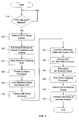
- FIG. 2 depicts an example process for supporting runtime migration of processors in the processing system of Figure 1 .
- the illustrated process begins after processing system 20 has booted and been configured to use CPU 22 as the active or primary processor and CPU 23 as the spare processor.
- Block 110 depicts CPU migration manager 62 determining the need for CPU migration, for instance in response to detecting a failing CPU component in CPU 22.
- CPU migration manager 62 instructs OS 50, through the system pause interface, to pause or stop all processor and device activities.
- OS 50 freezes the OS scheduler and puts all processors on the system into the idle state.
- OS 50 also puts all devices in inactive state, disabling device interrupt transactions. This step ensures that CPU migration manager 62 can safely swap the state of the CPU between the outgoing and the spare processors. This step also prevents any processors from generating inter-processor interrupts (IPIs), and it prevents devices from generating external interrupts during the migration.
- IPIs inter-processor interrupts
- CPU migration manager 62 saves away the contents of the architectural and potentially machine-specific CPU states for the outgoing processor, including writable and non-writable processor states needing to be transferred, into a non-paged memory location.
- alternative storage areas e.g., cache memory, nonvolatile (NV) RAM, etc. may be used as temporary storage for the state data.
- CPU migration manager 62 then on-lines and brings up spare processor 23, to prepare for swapping the CPU state from outgoing processor 22 to spare processor 23.
- the operations associated with block 126 may include initializing spare processor 23 to a known state, including initializing states of machine specific registers with help from platform firmware 58.
- the CPU migration manager may bring up the spare processor before saving the CPU states of the outgoing processor.
- CPU migration manager 62 then swaps the architecturally writable contents of the CPU states into spare processor 23, by restoring the previously saved writable CPU states of outgoing processor 22, as shown at block 128. Also, as shown at block 130, CPU migration manager 62 invokes the NWSMI for processor 23, to instruct swap controller 49 to load the saved state into spare processor 23. In response to that request, swap controller 49 loads into spare processor 23 the non-writable architected CPU states that were previously saved from outgoing processor 22, as shown at block 132. Since these are non-writable, swap controller 49 may need to provide a special interface to modify the un-writable CPU state. In one embodiment, the implementation for this interface may use MSRs in processor 23 to access and modify non-writable processor CPU state.
- CPU migration manager 62 uses the interrupt migration interface to instruct interrupt reprogrammer 31 and uncore 47 to modify the interrupt routing table logic in chipset 34 and processor 23.
- interrupt reprogrammer 31 and uncore 47 dynamically reprogram the necessary routing tables to correctly direct external interrupts to spare processor 23, as depicted at block 136.
- CPU migration manager 62 may then off-line outgoing processor 22 with help from platform firmware 58.
- CPU migration manager 62 then notifies OS 50 of the completion of the CPU migration flow through the system pause interface.
- the implementation for this interface may use an ACPI notification mechanism.
- the CPU migration manager may simply use an OS API to interface with the OS.
- OS 50 activates the devices including the external interrupt transactions and unfreezes the OS scheduler to start utilizing spare processor 23, as shown at block 142.
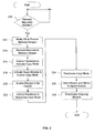
- Figure 3 depicts an example process for supporting runtime migration of memory modules in the processing system of Figure 1 .
- the illustrated process begins after processing system 20 has booted and been configured to use memory module 26A as an active or primary memory module and memory module 26B as a spare memory module.
- Block 210 depicts memory migration manager 64 determining the need for memory migration, for instance in response to detecting that memory module 26A is failing.
- memory controller 33 includes a mirror module 35.
- the mirror module may be configurable to mirror only writes, or to mirror reads and writes.
- the memory controller may use a conventional mirror module to support memory mirroring in a memory migration solution that uses help from the operating system.
- the memory controller and/or other components may be integrated into the CPU.
- the mirror copy mode of mirror module 35 may be enabled and disabled through an interface to the system software (e.g., OS 50). This interface may be referred to as a mirror mode selection interface.
- the mirror mode selection interface is implemented using memory or I/O mapped memory device registers.
- the mirror mode selection interface may be implemented differently, such as through abstraction into a higher level interface, such as an ACPI method or a firmware API.
- the spare memory module When the mirror copy mode is enabled, the spare memory module is activated and the memory contents are forwarded from the outgoing memory module to the spare memory module for every read operation. Also, every write goes to both the outgoing and spare memory modules when the mirror copy mode is enabled.
- the spare memory module Once the spare memory module has received the necessary data, mirror copy mode is disabled, the outgoing memory module is deactivated, and the memory decoders are reprogrammed to make memory writes and reads go directly to the spare memory module.
- one embodiment may include copy hardware based on write copy, and another embodiment may use hardware to fully automate the copy function without using any software.
- OS 50 also participates in the memory migration process. For instance, OS 50 may remove the memory usage of the paged memory ranges and may provide memory read operations for the memory ranges that need to be migrated. An implementation may choose to implement this operating system function with help from device driver modules, such as a memory driver 54, as shown in Figure 1 .
- device driver modules such as a memory driver 54
- memory migration manager 64 notifies OS 50 of the need of memory migration, and specifies the memory ranges that need to be migrated (e.g., the memory ranges residing on outgoing memory module 26A).
- the memory migration manager utilizes an ACPI mechanism to notify the OS of the need for memory migration and to communicate what memory ranges need to be migrated.
- Another implementation may define an API between the memory migration manager and the operating system for this purpose.
- OS 50 determines which of the specified memory ranges actually need to be migrated, and which memory ranges can simply be removed from usage by the operating system, device drivers, and applications, as shown at block 214. For instance, OS 50 may remove usages of free memory pool page ranges and non-dirty page-able memory ranges to reduce the amount of data that needs to be migrated. In one embodiment, OS 50 removes such usages by implementing such logic into the virtual memory management algorithm of its memory manager. For instance, in the example embodiment, OS 50 has a memory manager for maintaining a database to keep track of what memory ranges are free to be allocated (free memory pool rages) and what memory ranges have already copied contents on the disk ((non-dirty page-able memory ranges). By inspecting this database, OS 50 can determine which memory ranges have no memory contents to be preserved and do not need to be migrated.
- OS 50 may then invoke the mirror mode selection interface to activate the mirror copy mode function of mirror module 35 in memory controller 33.
- Memory controller 33 then activates spare memory module 26B and enables the code mode of mirror module 35 for forwarding memory contents from outgoing memory module 26A to spare memory module 26B.
- OS 50 then selectively reads the memory ranges with data that needs to be copied from outgoing memory module 26A to spare memory module 26B.
- read operations from the mirror module may not necessarily detect data that is already cached. Therefore, cache flush operations may be used prior to the read operations described above, to make the necessary memory data visible to the mirror module.
- the OS may need to perform memory read followed by memory write operations. More specifically, the OS may need to utilize an atomic read and write instruction, to avoid race conditions with agents (e.g., CPU or DMA) that may access the same memory address at the same time. Alternatively, the control logic to stop or pause processor and device activities used for the processor migration can be used to eliminate this race condition.
- to "access" memory means to read from memory or to write to memory.
- OS 50 invokes the mirror mode selection interface to notify memory controller 33 that memory migration operations have been completed.
- memory controller 33 then deactivates the memory mirror copy mode.
- Memory controller 33 reprograms the memory decoders to make memory writes and reads go directly to the spare memory module, as shown at block 226.
- Memory controller 33 also disables outgoing memory module 26A, as shown at block 228.
- Outgoing memory module 26A can then be off-lined, taken out, and possibly replaced. Memory usage may then be migrated back to the new memory module by memory migration manager 64.
- CPUs and memory modules may be replaced in a processing system with a shrink-wrapped OS without performing a system shutdown.
- runtime CPU and memory module replacement can be supported without requiring development of new device drivers and applications with new OS APIs. Consequently, the platform need not lose backward compatibility with existing device drivers and applications.
- the platform can provide for runtime memory module replacement without using full memory mirroring.
- Full memory mirroring is an expensive approach that requires entire memory modules to be paired with mirror memory modules all the time. Full mirroring may also adversely affect memory performance.
- Alternative embodiments of the invention also include machine accessible media encoding instructions for performing the operations of the invention. Such embodiments may also be referred to as program products.
- Such machine accessible media may include, without limitation, storage media such as floppy disks, hard disks, CD-ROMs, ROM, and RAM; and other detectable arrangements of particles manufactured or formed by a machine or device. Instructions may also be used in a distributed environment, and may be stored locally and/or remotely for access by single or multi-processor machines.
Abstract
Description
- The present disclosure relates generally to the field of data processing, and more particularly to methods and related apparatus for supporting runtime migration of processors and/or memory modules.
- Runtime replacement of processors and runtime replacement of memory modules are two of the key innovative features envisioned in high-end server systems for supporting reliability, availability, and serviceability (RAS). When a processing system supports runtime replacement of processors and memory modules, a faulty processor or memory module can be replaced without shutting down the system. However, it may not be possible to implement runtime replacement of processors and memory modules without providing many different software components in the processing system with special control logic for supporting such functionality. For instance, special control logic may be needed in the applications, in the operating system (OS), and in the device drivers.
- When all of the hardware and software for a computer system is built by the same company, that company may be said to provide a vertical solution. Specifically, for purposes of this disclosure, the term "vertical solution" denotes a high-end server with a proprietary OS and vertical device driver and application development environments that are controlled from top to bottom by a single company. A small number of companies may currently build vertical solutions which include the necessary hardware and software features to enable runtime replacement of processors and memory modules. Those companies may include International Business Machines Corp. (IBM), the Hewlett-Packard Company (HP), Sun Microsystems, Inc. (Sun), and NEC Corp. (NEC). However, such a vertical solution is proprietary by nature and does not translate to the horizontal market.
- A horizontal solution for this problem needs to run on standard high-volume servers which use an OS that was designed with standardized interfaces for use in a wide range of platforms. For purposes of this disclosure, an OS that features standardized interfaces for use in a wide range of platforms may be referred to as a shrink-wrapped OS. For example, the various OSs sold by Microsoft Corp. under the Windows trademark are considered shrink-wrapped OSs. The OSs sold by Red Hat, Inc. under the Linux trademark may also be considered shrink-wrapped OSs. For a shrink-wrapped OS, the binaries work with different platforms. Consequently, shrink-wrapped OSs need standardized interfaces, so drivers can be written by parties other than company that wrote the OS.
- However, when a data processing system or platform uses a shrink-wrapped OS, that platform may be unable to support runtime replacement of processors or memory modules. Some of the technical challenges associated with creating a platform that supports the runtime replacement of processors or memory modules while using a shrink-wrapped OS pertain to backward compatibility issues with legacy device drivers and applications.
- Features and advantages of the present invention will become apparent from the appended claims, the following detailed description of one or more example embodiments, and the corresponding figures, in which:
-
Figure 1 is a block diagram depicting an example data processing environment; and -
Figures 2 and3 are flowcharts depicting various aspects of example processes for supporting runtime migration of processors and/or memory modules in the processing system ofFigure 1 . - This disclosure describes one or more methods and apparatus to enable runtime migration of processors and memory modules in an OS assisted manner, using processor, chipset, and memory controller extensions.
- As used herein, the term "outgoing processor" refers to a processor that is to be replaced, and the term "spare processor" refers to a processor that will replace an outgoing processor. Similarly, the term "outgoing memory module" refers to a memory module that is to be replaced, and the term "spare memory module" refers to a memory module that will replace an outgoing memory module.
- Currently, processor resources are exposed to device drivers and applications through OS application program interfaces (APIs) with processor affinity. Legacy applications and drivers directly control the thread scheduling and interrupt bindings to make use of these processor resources. Also, when working with a shrink-wrapped OS, device drivers and applications can control the residency of physical pages, in order to interact with devices and perform direct memory access (DMA) operations on buffer memory using OS APIs. As a result, it may be impossible for a shrink-wrapped OS to remove any processor or memory resources without device driver and application support.
- However, making all applications and drivers cognizant of the processor and memory removal events may require the development of new OS APIs and the rewriting of device drivers and applications. It could take many years to complete such efforts. Further, inherent limitations may prevent a shrink-wrapped OS from migrating some specific processor and memory resources, in spite of migration cognizant drivers and applications. Some examples are bootstrap processor and 16-bit DMA target memory (0-1M).
- Another potential alternative would be to create a hardware and/or firmware-based solution that enables processor and memory migration without OS support, making such CPU and memory removal events completely transparent to the OS, the device drivers, and the applications. However, such solutions would be very complex to design, and may not in fact be practicable to implement. Some of the complexity pertains to transferring all the architecturally visible CPU states from one processor to another in a way that is completely transparent to the OS, the device drivers, and the applications. Additional complexity pertains to handling device interrupts without losing them and redirect in-flight interrupt transitions from an outgoing processor to a spare processor during runtime. In addition, it may not even be possible to make processor migration completely transparent to the OS, the device drivers, and the applications due to the potential long latency of the migration process. For instance, blocking external interrupts for a long time may result in OS, device driver, and application failures, due to various timeout issues. For transparent memory migration, a full hardware copy engine may be very expensive to build, while firmware routines to copy contents of memory may result in very long latency for the whole memory migration process. This latency may create a visible performance impact to the OS and applications during the memory migration process.
- This disclosure introduces a new way of implementing runtime replacement of processors and memory modules, for use in platforms that use shrink-wrapped OSs. For shrink-wrapped OS market segments, extensive re-writing of device drivers and applications seems an unacceptable proposition. The features described herein enable runtime replacement of processors and memory modules without the need for extensive re-writing of device drivers and applications.
- In an example embodiment, the platform includes a small number of processor and/or platform hardware feature extensions, and migration is performed with OS assistance. For example, this disclosure describes a processor hardware extension for swapping non-writable architected states, as well as chipset and uncore-level extensions for re- dynamically programming the interrupt routing tables. The term "uncore" refers to components of a multi-core chip other than the cores (e.g., the interconnect for the cores, the bus interfaces, etc.) This disclosure also describes a new way of implementing the runtime replacement of memory modules for platforms that use shrink-wrapped OSs. Memory migration is performed with OS assistance. For example, migration may involve use of a memory controller extension that supports the mirror copy mode feature, such as the feature originally designed to support memory mirroring. The memory controller may be used to enable selective copying of data from one memory module to another.
-
Figure 1 is a block diagram depicting an exampledata processing environment 12.Data processing environment 12 includes a localdata processing system 20 that includesvarious hardware components 80 andsoftware components 82. - The hardware components may include, for example, two or more processors or
CPUs core 42,core 44,core 46, andcore 48. Alternatively, a processing system may include one or more CPUs with a single processing core. The processing units may be implemented as processing cores, as Hyper-Threading (HT) technology, or as any other suitable technology for executing multiple threads simultaneously or substantially simultaneously. -
Processing system 20 may be controlled, at least in part, by input from conventional input devices, such as a keyboard, a pointing device such as a mouse, etc.Processing system 20 may also respond to directives received from other processing systems or other input sources or signals.Processing system 20 may utilize one or more connections to one or more remotedata processing systems 70, for example through a network interface controller (NIC) 32, a modem, or other communication ports or couplings. Processing systems may be interconnected by way of a physical and/orlogical network 72, such as a local area network (LAN), a wide area network (WAN), an intranet, the Internet, etc.Communications involving network 72 may utilize various wired and/or wireless short range or long range carriers and protocols, including radio frequency (RF), satellite, microwave, Institute of Electrical and Electronics Engineers (IEEE) 802.11, 802.16, 802.20, Bluetooth, optical, infrared, cable, laser, etc. Protocols for 802.11 may also be referred to as wireless fidelity (WiFi) protocols. Protocols for 802.16 may also be referred to as WiMAX or wireless metropolitan area network protocols. Information on WiMAX protocols is currently available at grouper.ieee.org/groups/802/16/published.html. - Within processing
system 20,processors flash memory 27 andhard disk drive 28. In the embodiment ofFigure 1 ,RAM 26 consists of multiple memory modules, such asmemory modules - In alternative embodiments, different numbers of memory modules may be used for RAM, and multiple nonvolatile memory devices and/or multiple disk drives may be used for nonvolatile storage. Suitable nonvolatile storage devices and/or media may include, without limitation, integrated drive electronics (IDE) and small computer system interface (SCSI) hard drives, optical storage, tapes, floppy disks, read-only memory (ROM), memory sticks, digital video disks (DVDs), biological storage, phase change memory (PCM), etc. As used herein, the term "nonvolatile storage" refers to disk drives, flash memory, and any other storage component that can retain data when the processing system is powered off. The term "nonvolatile memory" refers more specifically to memory devices (e.g., flash memory) that do not use rotating media but still can retain data when the processing system is powered off. The terms "flash memory" and "ROM" are used herein to refer broadly to nonvolatile memory devices such as erasable programmable ROM (EPROM), electrically erasable programmable ROM (EEPROM), flash ROM, etc.
-
Processors NIC 32, video controllers, IDE controllers, SCSI controllers, universal serial bus (USB) controllers, input/output (I/O) ports, input devices, output devices, etc.Processing system 20 may also include achipset 34 with one or more bridges or hubs, such as amemory controller hub 33, an I/O controller hub, a PCI root bridge, etc., for communicatively coupling system components. Memory controller hub (MCH) 33 may also be referred to as memory controller (MC) 33. - Some components, such as
NIC 32, for example, may be implemented as adapter cards with interfaces (e.g., a PCI connector) for communicating with a bus. Alternatively,NIC 32 and/or other devices may be implemented as embedded controllers, using components such as programmable or non-programmable logic devices or arrays, application-specific integrated circuits (ASICs), embedded computers, smart cards, etc. In alternative embodiments, processing systems may feature different numbers and/or combinations of cores, memory controllers, memory modules, etc. - As used herein, the terms "processing system" and "data processing system" are intended to broadly encompass a single machine, or a system of communicatively coupled machines or devices operating together. Example processing systems include, without limitation, distributed computing systems, supercomputers, high-performance computing systems, computing clusters, mainframe computers, mini-computers, client-server systems, personal computers (PCs), workstations, servers, portable computers, laptop computers, tablet computers, personal digital assistants (PDAs), telephones, handheld devices, entertainment devices such as audio and/or video devices, and other devices for processing and/or transmitting information.
- An embodiment of the invention is described herein with reference to or in conjunction with data such as instructions, functions, procedures, data structures, application programs, configuration settings, etc. When the data is accessed by a machine, the machine may respond by performing tasks, defining abstract data types or low-level hardware contexts, and/or performing other operations, as described in greater detail below. The data may be stored in volatile and/or nonvolatile data storage. As used herein, the term "program" covers a broad range of software components and constructs, including applications, modules, drivers, routines, subprograms, methods, processes, threads, and other types of software components. Also, the term "program" can be used to refer to a complete compilation unit (i.e., a set of instructions that can be compiled independently), a collection of compilation units, or a portion of a compilation unit. Thus, the term "program" may be used to refer to any collection of instructions which, when executed by a processing system, perform a desired operation or operations.
- The programs in
processing system 20 may be considered components of asoftware environment 82. For instance,data storage device 28 and/orflash memory 27 may include various sets of instructions which, when executed, perform various operations. Such sets of instructions may be referred to in general as software. - As illustrated in
Figure 1 , in the example embodiment, the programs orsoftware components 82 may includesystem firmware 58,OS 50, and one ormore applications 60.System firmware 58 may include boot firmware for managing the boot process, as well as runtime modules or instructions that can be executed after the OS boot code has been called.System firmware 58 may also be referred to as a basic input/output system (BIOS) 58. - In addition,
firmware 58 includes CPUmigration management software 62 and memorymigration management software 64. CPUmigration management software 62 may also be referred to as aCPU migration manager 62. Memorymigration management software 64 may also be referred to as amemory migration manager 64. In the embodiment ofFigure 1 ,CPU migration manager 62 and amemory migration manager 64 are implemented as runtime modules offirmware 58. - As described in greater detail below, in the example embodiment,
CPU migration manager 62 includes control logic to manage the entire flow of the CPU migration operations. In the example embodiment,CPU migration manager 62 runs at the highest privilege level (e.g., in ring 0). In alternative embodiments, CPU migration managers may be implemented partially or completely outside of the system firmware. For instance, the control logic may be implemented entirely in an OS, with device driver components; the control logic may be split between the firmware and the OS by dividing roles and responsibilities; etc. - As described in greater detail below,
memory migration manager 64 includes control logic to manage the entire flow of the memory migration operations. In the example embodiment,memory migration manager 62 runs at the highest privilege level (e.g., in ring 0, in a system management interrupt (SMI) context, etc.), from a platform management stack withinsystem firmware 58. In alternative embodiments, memory migration managers may be implemented partially or completely outside of the system firmware. For instance, the control logic may be implemented entirely in an OS, with device driver components. Alternatively, the control logic may also reside partially in one or more application agents. Alternatively, the control logic may be split between the firmware and the OS by dividing roles and responsibilities. - In the example embodiment,
processing system 20 is configured to useCPU 22 as the active processor andCPU 23 as the spare or backup processor. As indicated above, when the active processor needs to be swapped out, the active processor may be referred to as the outgoing processor. - As indicated above,
CPU 22 includesprocessing core 42 andprocessing core 44, whileCPU 23 includesprocessing core 46 andprocessing core 48. In addition to processing cores,CPU 22 includes anuncore 43 and aswap controller 45. Likewise,CPU 23 includes anuncore 47 and aswap controller 49.Swap controllers CPU migration manager 62 to store, in the CPUs, state data that would be substantially non-writeable in a conventional processor. For instance,CPU migration manager 62 can useswap controller 45 to swap substantially non-writable architected states which are visible to device drivers and applications between outgoing and spare processors. - An instance of a substantially non-writable architected state is the initial advanced programmable interface controller (APIC) identifier (ID) state in processors that support the x86 architecture. In such a processor, the initial APIC ID value is retrievable through use of the CPUID instruction, with the EAX register set to 1 (EAX=1). In particular, as explained on page 3 of the article entitled "Methods to Utilize Intel's Hyper-Threading Technology with Linux*" (available at www.intel.com/cd/ids/developer/asmo-na/eng/20354.htm?page=3):
- Each logical processor has a unique Advanced Programmable Interface Controller (APIC) ID. The APIC ID is initially assigned by the hardware at system reset and can be later reprogrammed by the BIOS or the operating system. On a processor that supports HT Technology, the CPUID instruction also provides the initial APIC ID for a logical processor prior to any changes by the BIOS or operating system.
- The other APIC ID, referred to herein as the "current APIC ID," can be "later reprogrammed by the BIOS or the operating system," as indicated above. However, even if the BIOS or the OS can reprogram the current APIC ID, in practice it cannot be written with an arbitrary value. Whether the current APIC ID can be written may be model specific. The current APIC ID value is also used by the platform for performing proper routing of the interrupts, and changing the value requires the interrupt routing table on the chipset or uncore to be reprogrammed. Therefore, the current APIC ID should only be modified by the interrupt reprogrammer and the uncore, as described in greater detail below with regard to block 136 in
Figure 2 ,. For instance, theIntel 64 and IA-32 Architecture Software Developers Manual (SDM), Vol.3A, section 8.4.6 (Local APIC) states the following: - In MP systems, the local APIC ID is also used as a processor ID by the BIOS and the operating system. Some processors permit software to modify the APIC ID. However, the ability of software to modify the APIC ID is processor model specific. Because of this, operating system software should avoid writing to the local APIC ID register.
- In the example embodiment,
swap controllers processors swap controller 45 may provide an interface to a machine specific register (MSR) inprocessor 22 to hold the initial APIC ID value that will be reported in response to the CPUID instruction executed with EAX=1. In one embodiment, the interfaces provided byswap controllers CPU migration manager 62. Accordingly, such an interface may be referred to as a non-writeable state migration interface. - Additional substantially non-writable state values that a CPU migration manager may update through an interface such as that provided by
swap controller - In the embodiment of
Figure 1 ,chipset 34 includes an interruptreprogrammer 31. Interruptreprogrammer 31 serves a platform processor function to reprogram interrupt routing tables dynamically. Uncores 43 and 45 may also include control logic for dynamically reprogramming interrupt routing tables. - A typical multi-processor or multi-core platform typically includes interrupt routing table logic to route external interrupts to correct processor destinations. Dynamic re-programmability of the interrupt routing table logic enables re-routing of external interrupts from outgoing processors to spare processors for the CPU migration. This interrupt routing reprogramming function can be implemented at the chipset and processor's uncore levels and can be exposed to the migration management software through chipset registers and processor's uncore registers. An interface for such communications may be referred to as an interrupt migration interface. In one embodiment, the interrupt migration interface may be implemented with a firmware API.
-
OS 50 includes control logic to stop or pause processor and device activities including interrupt transactions during a migration operation. In particular,OS 50 stops or pauses processor activity by freezing the OS thread scheduler and putting the processors in the idle state, andOS 50 stops or pauses device activity by stopping device functions including the DMA and interrupt transactions. In one embodiment, the OS uses more or less conventional sleep functionality (e.g., system hibernation) to pause the processor and device activities. - The interface that
CPU migration manager 62 uses to instructOS 50 to pause processor and device activities prior to CPU migration may be referred to as a system pause interface. In one embodiment, the system pause interface may be implemented using a more or less conventional Advanced Configuration and Power Interface (ACPI) notification mechanism, which may be invoked directly fromplatform firmware 58. Additional details about ACPI may be obtained from the Advanced Configuration And Power Interface Specification, Revision 3.0b, dated October 10, 2006, available at www.acpi.info/spec.htm. An alternative implementation may define a new OS API to allow applications or device drivers to initiate this operating system request. - As indicated above,
CPU migration manager 62 manages the flow of the CPU migration operations. An instance of this software component may also interact with an out-of-band platform management software stack. As described in greater detail below, when it is driving the CPU migration flow,CPU migration manager 62 invokes the non-writable state migration interface (NWSMI), the interrupt migration interface, and the system pause interface, and may interact withswap controllers reprogrammer 31, and withOS 50. -
Figure 2 depicts an example process for supporting runtime migration of processors in the processing system ofFigure 1 . The illustrated process begins after processingsystem 20 has booted and been configured to useCPU 22 as the active or primary processor andCPU 23 as the spare processor. -
Block 110 depictsCPU migration manager 62 determining the need for CPU migration, for instance in response to detecting a failing CPU component inCPU 22. Once the decision is made for the CPU migration,CPU migration manager 62 instructsOS 50, through the system pause interface, to pause or stop all processor and device activities. As shown atblock 120, in response to the request fromCPU migration manager 62,OS 50 freezes the OS scheduler and puts all processors on the system into the idle state.OS 50 also puts all devices in inactive state, disabling device interrupt transactions. This step ensures thatCPU migration manager 62 can safely swap the state of the CPU between the outgoing and the spare processors. This step also prevents any processors from generating inter-processor interrupts (IPIs), and it prevents devices from generating external interrupts during the migration. - As shown at
block 124, afterOS 50 freezes the processor and device activities,CPU migration manager 62 saves away the contents of the architectural and potentially machine-specific CPU states for the outgoing processor, including writable and non-writable processor states needing to be transferred, into a non-paged memory location. However, in alternative embodiments, alternative storage areas (e.g., cache memory, nonvolatile (NV) RAM, etc.) may be used as temporary storage for the state data. - As indicated at
block 126,CPU migration manager 62 then on-lines and brings upspare processor 23, to prepare for swapping the CPU state from outgoingprocessor 22 to spareprocessor 23. The operations associated withblock 126 may include initializingspare processor 23 to a known state, including initializing states of machine specific registers with help fromplatform firmware 58. In an alternative embodiment, the CPU migration manager may bring up the spare processor before saving the CPU states of the outgoing processor. - After
spare processor 23 is on line,CPU migration manager 62 then swaps the architecturally writable contents of the CPU states intospare processor 23, by restoring the previously saved writable CPU states ofoutgoing processor 22, as shown atblock 128. Also, as shown atblock 130,CPU migration manager 62 invokes the NWSMI forprocessor 23, to instructswap controller 49 to load the saved state intospare processor 23. In response to that request,swap controller 49 loads intospare processor 23 the non-writable architected CPU states that were previously saved fromoutgoing processor 22, as shown atblock 132. Since these are non-writable,swap controller 49 may need to provide a special interface to modify the un-writable CPU state. In one embodiment, the implementation for this interface may use MSRs inprocessor 23 to access and modify non-writable processor CPU state. - Then, as shown at
block 134,CPU migration manager 62 uses the interrupt migration interface to instruct interruptreprogrammer 31 and uncore 47 to modify the interrupt routing table logic inchipset 34 andprocessor 23. In response to that request, interruptreprogrammer 31 and uncore 47 dynamically reprogram the necessary routing tables to correctly direct external interrupts to spareprocessor 23, as depicted atblock 136. As shown atblock 138,CPU migration manager 62 may then off-lineoutgoing processor 22 with help fromplatform firmware 58. - As shown at
block 140,CPU migration manager 62 then notifiesOS 50 of the completion of the CPU migration flow through the system pause interface. In one embodiment, the implementation for this interface may use an ACPI notification mechanism. In another embodiment, the CPU migration manager may simply use an OS API to interface with the OS. In response to the unpause or resume request,OS 50 activates the devices including the external interrupt transactions and unfreezes the OS scheduler to start utilizingspare processor 23, as shown atblock 142. -
Figure 3 depicts an example process for supporting runtime migration of memory modules in the processing system ofFigure 1 . The illustrated process begins after processingsystem 20 has booted and been configured to usememory module 26A as an active or primary memory module andmemory module 26B as a spare memory module.Block 210 depictsmemory migration manager 64 determining the need for memory migration, for instance in response to detecting thatmemory module 26A is failing. - As illustrated in
Figure 1 ,memory controller 33 includes amirror module 35. In various embodiments, the mirror module may be configurable to mirror only writes, or to mirror reads and writes. In some embodiments, the memory controller may use a conventional mirror module to support memory mirroring in a memory migration solution that uses help from the operating system. In some embodiments, the memory controller and/or other components may be integrated into the CPU. - The mirror copy mode of
mirror module 35 may be enabled and disabled through an interface to the system software (e.g., OS 50). This interface may be referred to as a mirror mode selection interface. In one embodiment, the mirror mode selection interface is implemented using memory or I/O mapped memory device registers. In another embodiment, the mirror mode selection interface may be implemented differently, such as through abstraction into a higher level interface, such as an ACPI method or a firmware API. - When the mirror copy mode is enabled, the spare memory module is activated and the memory contents are forwarded from the outgoing memory module to the spare memory module for every read operation. Also, every write goes to both the outgoing and spare memory modules when the mirror copy mode is enabled. Once the spare memory module has received the necessary data, mirror copy mode is disabled, the outgoing memory module is deactivated, and the memory decoders are reprogrammed to make memory writes and reads go directly to the spare memory module.
- In alternative embodiments, other mirroring techniques may be used. For instance, one embodiment may include copy hardware based on write copy, and another embodiment may use hardware to fully automate the copy function without using any software.
- In the example embodiment,
OS 50 also participates in the memory migration process. For instance,OS 50 may remove the memory usage of the paged memory ranges and may provide memory read operations for the memory ranges that need to be migrated. An implementation may choose to implement this operating system function with help from device driver modules, such as amemory driver 54, as shown inFigure 1 . - As indicated at
block 212 ofFigure 3 , once the decision is made for memory migration,memory migration manager 64 notifiesOS 50 of the need of memory migration, and specifies the memory ranges that need to be migrated (e.g., the memory ranges residing onoutgoing memory module 26A). In one embodiment, the memory migration manager utilizes an ACPI mechanism to notify the OS of the need for memory migration and to communicate what memory ranges need to be migrated. Another implementation may define an API between the memory migration manager and the operating system for this purpose. -
OS 50 then determines which of the specified memory ranges actually need to be migrated, and which memory ranges can simply be removed from usage by the operating system, device drivers, and applications, as shown atblock 214. For instance,OS 50 may remove usages of free memory pool page ranges and non-dirty page-able memory ranges to reduce the amount of data that needs to be migrated. In one embodiment,OS 50 removes such usages by implementing such logic into the virtual memory management algorithm of its memory manager. For instance, in the example embodiment,OS 50 has a memory manager for maintaining a database to keep track of what memory ranges are free to be allocated (free memory pool rages) and what memory ranges have already copied contents on the disk ((non-dirty page-able memory ranges). By inspecting this database,OS 50 can determine which memory ranges have no memory contents to be preserved and do not need to be migrated. - As depicted at
block 216,OS 50 may then invoke the mirror mode selection interface to activate the mirror copy mode function ofmirror module 35 inmemory controller 33.Memory controller 33 then activatesspare memory module 26B and enables the code mode ofmirror module 35 for forwarding memory contents fromoutgoing memory module 26A to sparememory module 26B. As shown atblock 220,OS 50 then selectively reads the memory ranges with data that needs to be copied fromoutgoing memory module 26A to sparememory module 26B. However, for a processor that has internal cache, read operations from the mirror module may not necessarily detect data that is already cached. Therefore, cache flush operations may be used prior to the read operations described above, to make the necessary memory data visible to the mirror module. - Alternatively, if the mirroring configuration does not mirror both memory reads and writes, but only mirrors writes, the OS may need to perform memory read followed by memory write operations. More specifically, the OS may need to utilize an atomic read and write instruction, to avoid race conditions with agents (e.g., CPU or DMA) that may access the same memory address at the same time. Alternatively, the control logic to stop or pause processor and device activities used for the processor migration can be used to eliminate this race condition. For purposes of this disclosure, to "access" memory means to read from memory or to write to memory.
- Referring again to the embodiment of
Figure 3 , as depicted atblock 222, afterOS 50 has read the necessary memory locations to causemirror module 35 to migrate the data in those memory ranges,OS 50 invokes the mirror mode selection interface to notifymemory controller 33 that memory migration operations have been completed. As shown atblock 224,memory controller 33 then deactivates the memory mirror copy mode.Memory controller 33 then reprograms the memory decoders to make memory writes and reads go directly to the spare memory module, as shown atblock 226.Memory controller 33 also disablesoutgoing memory module 26A, as shown atblock 228. -
Outgoing memory module 26A can then be off-lined, taken out, and possibly replaced. Memory usage may then be migrated back to the new memory module bymemory migration manager 64. - Thus, CPUs and memory modules may be replaced in a processing system with a shrink-wrapped OS without performing a system shutdown. Furthermore, runtime CPU and memory module replacement can be supported without requiring development of new device drivers and applications with new OS APIs. Consequently, the platform need not lose backward compatibility with existing device drivers and applications.
- In addition, the platform can provide for runtime memory module replacement without using full memory mirroring. Full memory mirroring is an expensive approach that requires entire memory modules to be paired with mirror memory modules all the time. Full mirroring may also adversely affect memory performance.
- In light of the principles and example embodiments described and illustrated herein, it will be recognized that the described embodiments can be modified in arrangement and detail without departing from such principles. Also, although the foregoing discussion has focused on particular embodiments, other configurations are contemplated as well. Even though expressions such as "in one embodiment," "in another embodiment," or the like are used herein, these phrases are meant to generally reference embodiment possibilities, and are not intended to limit the invention to particular embodiment configurations. As used herein, these terms may reference the same or different embodiments that are combinable into other embodiments.
- Similarly, although example processes have been described with regard to particular operations performed in a particular sequence, numerous modifications could be applied to those processes to derive numerous alternative embodiments of the present invention. For example, alternative embodiments may include processes that use fewer than all of the disclosed operations, processes that use additional operations, processes that use the same operations in a different sequence, and processes in which the individual operations disclosed herein are combined, subdivided, or otherwise altered.
- Alternative embodiments of the invention also include machine accessible media encoding instructions for performing the operations of the invention. Such embodiments may also be referred to as program products. Such machine accessible media may include, without limitation, storage media such as floppy disks, hard disks, CD-ROMs, ROM, and RAM; and other detectable arrangements of particles manufactured or formed by a machine or device. Instructions may also be used in a distributed environment, and may be stored locally and/or remotely for access by single or multi-processor machines.
- It should also be understood that the hardware and software components depicted herein represent functional elements that are reasonably self-contained so that each can be designed, constructed, or updated substantially independently of the others. In alternative embodiments, many of the components may be implemented as hardware, software, or combinations of hardware and software for providing the functionality described and illustrated herein. The hardware, software, or combinations of hardware and software for performing the operations of the invention may also be referred to as logic or control logic.
- In view of the wide variety of useful permutations that may be readily derived from the example embodiments described herein, this detailed description is intended to be illustrative only, and should not be taken as limiting the scope of the invention. What is claimed as the invention, therefore, is all implementations that come within the scope and spirit of the following claims and all equivalents to such implementations.
Claims (15)
- A method for switching to a spare processor during runtime, the method comprising:determining that execution should be migrated off of an active processor in a processing system;after determining that execution should be migrated off of the active processor, pausing an operating system (OS) scheduler in the processing system, pausing at least one device in the processing system, and putting the active processor into an idle state;saving state data from writable and substantially non-writable stores in the active processor, to a store outside of the active processor;starting a spare processor in the processing system;loading the state data saved from the writeable store of the active processor to the spare processor;loading the state data saved from the substantially non-writeable store of active processor to the spare processor;reprogramming interrupt routing table logic for the processing system to direct external interrupts to the spare processor;off-lining the active processor;resuming the device; andresuming the OS scheduler.
- A method according to claim 1, wherein the operation of determining that execution should be migrated off of the active processor is performed by system firmware in the processing system.
- A method according to claim 2, further comprising:sending a pause request from the system firmware to the OS in response to determining that execution should be migrated off of the active processor.
- A method according to claim 3, further comprising:receiving a resume request from the system firmware at the OS; andresuming the device in response to the receiving the resume request from the system firmware.
- A method according to claim 3, further comprising:putting all active processors in the processing system into an idle state, and pausing all devices in the processing system, before loading the state data from the substantially non-writeable store of active processor into the spare processor.
- A method according to claim 1, wherein the operation of saving state data from writable and substantially non-writable stores in the active processor is performed after the active processor has entered the idle state.
- A method according to claim 1, wherein the operation of reprogramming interrupt routing table logic for the processing system comprises:reprogramming interrupt routing table logic in a chipset of the processing system; andreprogramming interrupt routing table logic in an uncore of the spare processor.
- A method according to claim 1, further comprising:after resuming the OS scheduler, dispatching threads to the spare processor for execution.
- A processing system that can switch to a spare processor during runtime, the processing system comprising:a first processor to serve as an active processor operable to execute an operating system (OS);a second processor to serve as a spare processor;at least one device;data storage;one or more communication pathways in communication with the first processor, the second processor, the device, and the data storage;control logic stored at least partially in the data storage, the control logic operable to perform operations comprising:determining that execution should be migrated off of the active processor;after determining that execution should be migrated off of the active processor, pausing a scheduler in the OS, pausing the device, and putting the active processor into an idle state;saving state data from writable and substantially non-writable stores in the active processor, to a store outside of the active processor;starting the spare processor;loading the state data saved from the writeable store of the active processor to the spare processor;loading the state data saved from the substantially non-writeable store of active processor to the spare processor;reprogramming interrupt routing table logic for the processing system to direct external interrupts to the spare processor;off-lining the active processor;unpausing the device; andunpausing the OS scheduler.
- A processing system according to claim 9, further comprising:the OS scheduler operable to dispatch threads to the spare processor for execution after the OS scheduler has been resumed.
- A processing system according to claim 9, wherein at least a portion of the control logic comprises system firmware.
- A processing system according to claim 9, further comprising the control logic operable to perform operations comprising:putting all active processors in the processing system into an idle state, and pausing all devices in the processing system, before loading the state data from the substantially non-writeable store of active processor into the spare processor.
- A processing system according to claim 9, further comprising:a chipset in communication with at least one of the communication pathways, the chipset to contain interrupt routing table logic; andan uncore in the spare processor, the uncore to contain interrupt routing table logic;the control logic to reprogram interrupt routing table logic for the processing system to direct external interrupts to the spare processor by reprogramming the interrupt routing table logic in the chipset and the interrupt routing table logic in the uncore of the spare processor.
- An apparatus, comprising:a machine-accessible medium; andinstructions in the machine-accessible medium, wherein the instructions, when executed by a processing system having an active processor and a spare processor, cause the processing system to perform operations comprising:determining that execution should be migrated off of the active processor;after determining that execution should be migrated off of the active processor, pausing an operating system (OS) scheduler in the processing system, pausing at least one device in the processing system, and putting the active processor into an idle state;saving state data from writable and substantially non-writable stores in the active processor, to a store outside of the active processor;starting the spare processor;loading the state data saved from the writeable store of the active processor to the spare processor;loading the state data saved from the substantially non-writeable store of active processor to the spare processor;reprogramming interrupt routing table logic for the processing system to direct external interrupts to the spare processor;off-lining the active processor;resuming the device;resuming the OS scheduler; anddispatching threads to the spare processor for execution.
- An apparatus according to claim 14, wherein the instructions cause the processing system to reprogram interrupt routing table logic for the processing system to direct external interrupts to the spare processor by (a) reprogramming interrupt routing table logic in a chipset of the processing system and (b) reprogramming interrupt routing table logic in an uncore of the spare processor.
Applications Claiming Priority (1)
| Application Number | Priority Date | Filing Date | Title |
|---|---|---|---|
| US11/772,155 US8296768B2 (en) | 2007-06-30 | 2007-06-30 | Method and apparatus to enable runtime processor migration with operating system assistance |
Publications (2)
| Publication Number | Publication Date |
|---|---|
| EP2009551A1 true EP2009551A1 (en) | 2008-12-31 |
| EP2009551B1 EP2009551B1 (en) | 2010-02-24 |
Family
ID=39734965
Family Applications (1)
| Application Number | Title | Priority Date | Filing Date |
|---|---|---|---|
| EP08251110A Not-in-force EP2009551B1 (en) | 2007-06-30 | 2008-03-27 | Method and apparatus to enable runtime processor migration with operating system assistance |
Country Status (5)
| Country | Link |
|---|---|
| US (1) | US8296768B2 (en) |
| EP (1) | EP2009551B1 (en) |
| CN (1) | CN101364189B (en) |
| AT (1) | ATE459047T1 (en) |
| DE (1) | DE602008000690D1 (en) |
Cited By (5)
| Publication number | Priority date | Publication date | Assignee | Title |
|---|---|---|---|---|
| US8051234B2 (en) * | 2007-01-16 | 2011-11-01 | Renesas Electronics Corporation | Multiprocessor system |
| US20150052409A1 (en) * | 2013-08-14 | 2015-02-19 | Advantest Corporation | Flexible interrupt generation mechanism |
| CN104506440A (en) * | 2014-12-26 | 2015-04-08 | 成都致云科技有限公司 | Data package transmitting method and routing list correcting method for router |
| FR3028066A1 (en) * | 2014-11-04 | 2016-05-06 | Commissariat Energie Atomique | METHOD AND DEVICE FOR FAULT TOLERANCE ON ELECTRONIC COMPONENTS |
| EP3079066A1 (en) * | 2015-04-10 | 2016-10-12 | Politechnika Lodzka | System of electronic modules having a redundant configuration |
Families Citing this family (27)
| Publication number | Priority date | Publication date | Assignee | Title |
|---|---|---|---|---|
| KR100901286B1 (en) | 2008-12-23 | 2009-06-09 | 어울림정보기술주식회사 | Running and dynamically process real located system and method by changing load of individual core at the multi-core processor |
| CN101504618B (en) * | 2009-02-26 | 2011-04-27 | 浙江大学 | Multi-core processor oriented real-time thread migration method |
| US8332854B2 (en) * | 2009-05-19 | 2012-12-11 | Microsoft Corporation | Virtualized thread scheduling for hardware thread optimization based on hardware resource parameter summaries of instruction blocks in execution groups |
| CN102043670A (en) * | 2009-10-22 | 2011-05-04 | 系微股份有限公司 | Method for switching different operation systems by computer |
| TW201222254A (en) * | 2010-11-26 | 2012-06-01 | Inventec Corp | Method for protecting data in damaged memory cells by dynamically switching memory mode |
| US20130007768A1 (en) * | 2011-07-02 | 2013-01-03 | Ramakrishna Saripalli | Atomic operations on multi-socket platforms |
| US10311027B2 (en) | 2011-09-23 | 2019-06-04 | Open Invention Network, Llc | System for live-migration and automated recovery of applications in a distributed system |
| GB2495079A (en) | 2011-09-23 | 2013-04-03 | Hybrid Logic Ltd | Live migration of applications and file systems in a distributed system |
| US10331801B2 (en) | 2011-09-23 | 2019-06-25 | Open Invention Network, Llc | System for live-migration and automated recovery of applications in a distributed system |
| US8799710B2 (en) * | 2012-06-28 | 2014-08-05 | International Business Machines Corporation | 3-D stacked multiprocessor structures and methods to enable reliable operation of processors at speeds above specified limits |
| US9952579B2 (en) * | 2013-02-15 | 2018-04-24 | Mitsubishi Electric Corporation | Control device |
| KR102052964B1 (en) * | 2013-03-12 | 2019-12-06 | 삼성전자 주식회사 | Method and system for scheduling computing |
| CN105009086B (en) * | 2014-03-10 | 2019-01-18 | 华为技术有限公司 | A kind of method, computer and switching device for realizing processor switching |
| CN103984908B (en) * | 2014-05-05 | 2017-03-08 | 上海新储集成电路有限公司 | A kind of South Bridge chip and its application process |
| US9910700B2 (en) * | 2015-08-26 | 2018-03-06 | Netapp, Inc. | Migration between CPU cores |
| US10459759B2 (en) | 2015-08-26 | 2019-10-29 | Netapp, Inc. | Migration between CPU cores |
| US10042720B2 (en) | 2016-02-22 | 2018-08-07 | International Business Machines Corporation | Live partition mobility with I/O migration |
| US10002018B2 (en) | 2016-02-23 | 2018-06-19 | International Business Machines Corporation | Migrating single root I/O virtualization adapter configurations in a computing system |
| US10042723B2 (en) | 2016-02-23 | 2018-08-07 | International Business Machines Corporation | Failover of a virtual function exposed by an SR-IOV adapter |
| US10025584B2 (en) | 2016-02-29 | 2018-07-17 | International Business Machines Corporation | Firmware management of SR-IOV adapters |
| US20170300101A1 (en) * | 2016-04-14 | 2017-10-19 | Advanced Micro Devices, Inc. | Redirecting messages from idle compute units of a processor |
| US9720863B1 (en) | 2016-10-21 | 2017-08-01 | International Business Machines Corporation | Migrating MMIO from a source I/O adapter of a source computing system to a destination I/O adapter of a destination computing system |
| US9720862B1 (en) | 2016-10-21 | 2017-08-01 | International Business Machines Corporation | Migrating interrupts from a source I/O adapter of a computing system to a destination I/O adapter of the computing system |
| US9715469B1 (en) * | 2016-10-21 | 2017-07-25 | International Business Machines Corporation | Migrating interrupts from a source I/O adapter of a source computing system to a destination I/O adapter of a destination computing system |
| US10353815B2 (en) | 2017-05-26 | 2019-07-16 | Microsoft Technology Licensing, Llc | Data security for multiple banks of memory |
| US10587575B2 (en) | 2017-05-26 | 2020-03-10 | Microsoft Technology Licensing, Llc | Subsystem firewalls |
| US10346345B2 (en) * | 2017-05-26 | 2019-07-09 | Microsoft Technology Licensing, Llc | Core mapping |
Citations (4)
| Publication number | Priority date | Publication date | Assignee | Title |
|---|---|---|---|---|
| US6061711A (en) * | 1996-08-19 | 2000-05-09 | Samsung Electronics, Inc. | Efficient context saving and restoring in a multi-tasking computing system environment |
| US20020016863A1 (en) | 1997-02-19 | 2002-02-07 | Scott Lurndal | Multicomputer system |
| US6622259B1 (en) * | 2000-07-14 | 2003-09-16 | International Business Machines Corporation | Non-disruptive migration of coordinator services in a distributed computer system |
| US20030233433A1 (en) * | 2002-02-21 | 2003-12-18 | Halpern Eric M. | Systems and methods for migratable services |
Family Cites Families (6)
| Publication number | Priority date | Publication date | Assignee | Title |
|---|---|---|---|---|
| EP0441087B1 (en) * | 1990-02-08 | 1995-08-16 | International Business Machines Corporation | Checkpointing mechanism for fault-tolerant systems |
| DE4309532C2 (en) * | 1992-03-25 | 1996-10-31 | Intel Corp | Method for backing up a system image of a computer system on a permanent storage device and a computer system |
| CN1208721C (en) * | 2003-09-19 | 2005-06-29 | 清华大学 | Graded task switching method based on PowerPC processor structure |
| US7251746B2 (en) * | 2004-01-21 | 2007-07-31 | International Business Machines Corporation | Autonomous fail-over to hot-spare processor using SMI |
| US7480643B2 (en) * | 2005-12-22 | 2009-01-20 | International Business Machines Corporation | System and method for migrating databases |
| US7721049B2 (en) * | 2006-03-27 | 2010-05-18 | Kabuhsiki Kaisha Toshiba | Disk drive write method |
-
2007
- 2007-06-30 US US11/772,155 patent/US8296768B2/en active Active
-
2008
- 2008-03-27 DE DE602008000690T patent/DE602008000690D1/en active Active
- 2008-03-27 AT AT08251110T patent/ATE459047T1/en not_active IP Right Cessation
- 2008-03-27 EP EP08251110A patent/EP2009551B1/en not_active Not-in-force
- 2008-06-30 CN CN2008102103488A patent/CN101364189B/en not_active Expired - Fee Related
Patent Citations (4)
| Publication number | Priority date | Publication date | Assignee | Title |
|---|---|---|---|---|
| US6061711A (en) * | 1996-08-19 | 2000-05-09 | Samsung Electronics, Inc. | Efficient context saving and restoring in a multi-tasking computing system environment |
| US20020016863A1 (en) | 1997-02-19 | 2002-02-07 | Scott Lurndal | Multicomputer system |
| US6622259B1 (en) * | 2000-07-14 | 2003-09-16 | International Business Machines Corporation | Non-disruptive migration of coordinator services in a distributed computer system |
| US20030233433A1 (en) * | 2002-02-21 | 2003-12-18 | Halpern Eric M. | Systems and methods for migratable services |
Cited By (8)
| Publication number | Priority date | Publication date | Assignee | Title |
|---|---|---|---|---|
| US8051234B2 (en) * | 2007-01-16 | 2011-11-01 | Renesas Electronics Corporation | Multiprocessor system |
| US20150052409A1 (en) * | 2013-08-14 | 2015-02-19 | Advantest Corporation | Flexible interrupt generation mechanism |
| US9449714B2 (en) * | 2013-08-14 | 2016-09-20 | Advantest Corporation | Flexible interrupt generation mechanism |
| FR3028066A1 (en) * | 2014-11-04 | 2016-05-06 | Commissariat Energie Atomique | METHOD AND DEVICE FOR FAULT TOLERANCE ON ELECTRONIC COMPONENTS |
| WO2016071329A1 (en) * | 2014-11-04 | 2016-05-12 | Commissariat A L'energie Atomique Et Aux Energies Alternatives | Fault tolerance method and device for electronic components |
| CN104506440A (en) * | 2014-12-26 | 2015-04-08 | 成都致云科技有限公司 | Data package transmitting method and routing list correcting method for router |
| CN104506440B (en) * | 2014-12-26 | 2017-12-26 | 成都致云科技有限公司 | The data packet sending method and routing table amending method of router |
| EP3079066A1 (en) * | 2015-04-10 | 2016-10-12 | Politechnika Lodzka | System of electronic modules having a redundant configuration |
Also Published As
| Publication number | Publication date |
|---|---|
| US8296768B2 (en) | 2012-10-23 |
| CN101364189A (en) | 2009-02-11 |
| ATE459047T1 (en) | 2010-03-15 |
| US20090007121A1 (en) | 2009-01-01 |
| EP2009551B1 (en) | 2010-02-24 |
| DE602008000690D1 (en) | 2010-04-08 |
| CN101364189B (en) | 2012-06-27 |
Similar Documents
| Publication | Publication Date | Title |
|---|---|---|
| EP2009551B1 (en) | Method and apparatus to enable runtime processor migration with operating system assistance | |
| US20090006793A1 (en) | Method And Apparatus To Enable Runtime Memory Migration With Operating System Assistance | |
| US7797555B2 (en) | Method and apparatus for managing power from a sequestered partition of a processing system | |
| CN101320314B (en) | Method and apparatus for quickly changing the power state of a data processing system | |
| EP2380081B1 (en) | Method and system for hibernation or suspend using a non-volatile-memory device | |
| US7865762B2 (en) | Methods and apparatus for handling errors involving virtual machines | |
| US6158000A (en) | Shared memory initialization method for system having multiple processor capability | |
| US7523323B2 (en) | Method and apparatus for quick resumption | |
| US9223738B2 (en) | Method, system, and apparatus for dynamic reconfiguration of resources | |
| US5297282A (en) | Resume processing function for the OS/2 operating system | |
| US7647509B2 (en) | Method and apparatus for managing power in a processing system with multiple partitions | |
| US20110113426A1 (en) | Apparatuses for switching the running of a virtual machine between multiple computer devices belonging to the same computer platform and the associated switching methods | |
| US20060294351A1 (en) | Migration of system images | |
| US20070150713A1 (en) | Methods and arrangements to dynamically modify the number of active processors in a multi-node system | |
| US8261053B2 (en) | Method and apparatus for maintaining a partition when booting another partition | |
| US20080126650A1 (en) | Methods and apparatus for parallel processing in system management mode | |
| US20190004818A1 (en) | Method of UEFI Shell for Supporting Power Saving Mode and Computer System thereof | |
| US11900097B2 (en) | Application downtime reduction using detached mode operation during operating system updates | |
| US20180232183A1 (en) | Techniques of emulating an acpi controller on a service processor | |
| JP2014531099A (en) | Switching operating context |
Legal Events
| Date | Code | Title | Description |
|---|---|---|---|
| PUAI | Public reference made under article 153(3) epc to a published international application that has entered the european phase |
Free format text: ORIGINAL CODE: 0009012 |
|
| 17P | Request for examination filed |
Effective date: 20080327 |
|
| AK | Designated contracting states |
Kind code of ref document: A1 Designated state(s): AT BE BG CH CY CZ DE DK EE ES FI FR GB GR HR HU IE IS IT LI LT LU LV MC MT NL NO PL PT RO SE SI SK TR |
|
| AX | Request for extension of the european patent |
Extension state: AL BA MK RS |
|
| 17Q | First examination report despatched |
Effective date: 20090219 |
|
| AKX | Designation fees paid |
Designated state(s): AT BE BG CH CY CZ DE DK EE ES FI FR GB GR HR HU IE IS IT LI LT LU LV MC MT NL NO PL PT RO SE SI SK TR |
|
| GRAP | Despatch of communication of intention to grant a patent |
Free format text: ORIGINAL CODE: EPIDOSNIGR1 |
|
| GRAS | Grant fee paid |
Free format text: ORIGINAL CODE: EPIDOSNIGR3 |
|
| GRAA | (expected) grant |
Free format text: ORIGINAL CODE: 0009210 |
|
| AK | Designated contracting states |
Kind code of ref document: B1 Designated state(s): AT BE BG CH CY CZ DE DK EE ES FI FR GB GR HR HU IE IS IT LI LT LU LV MC MT NL NO PL PT RO SE SI SK TR |
|
| REG | Reference to a national code |
Ref country code: GB Ref legal event code: FG4D |
|
| REG | Reference to a national code |
Ref country code: CH Ref legal event code: EP |
|
| REG | Reference to a national code |
Ref country code: IE Ref legal event code: FG4D |
|
| REF | Corresponds to: |
Ref document number: 602008000690 Country of ref document: DE Date of ref document: 20100408 Kind code of ref document: P |
|
| REG | Reference to a national code |
Ref country code: NL Ref legal event code: T3 |
|
| LTIE | Lt: invalidation of european patent or patent extension |
Effective date: 20100224 |
|
| PG25 | Lapsed in a contracting state [announced via postgrant information from national office to epo] |
Ref country code: LT Free format text: LAPSE BECAUSE OF FAILURE TO SUBMIT A TRANSLATION OF THE DESCRIPTION OR TO PAY THE FEE WITHIN THE PRESCRIBED TIME-LIMIT Effective date: 20100224 Ref country code: HR Free format text: LAPSE BECAUSE OF FAILURE TO SUBMIT A TRANSLATION OF THE DESCRIPTION OR TO PAY THE FEE WITHIN THE PRESCRIBED TIME-LIMIT Effective date: 20100224 Ref country code: NO Free format text: LAPSE BECAUSE OF FAILURE TO SUBMIT A TRANSLATION OF THE DESCRIPTION OR TO PAY THE FEE WITHIN THE PRESCRIBED TIME-LIMIT Effective date: 20100524 Ref country code: IS Free format text: LAPSE BECAUSE OF FAILURE TO SUBMIT A TRANSLATION OF THE DESCRIPTION OR TO PAY THE FEE WITHIN THE PRESCRIBED TIME-LIMIT Effective date: 20100624 |
|
| PG25 | Lapsed in a contracting state [announced via postgrant information from national office to epo] |
Ref country code: SI Free format text: LAPSE BECAUSE OF FAILURE TO SUBMIT A TRANSLATION OF THE DESCRIPTION OR TO PAY THE FEE WITHIN THE PRESCRIBED TIME-LIMIT Effective date: 20100224 Ref country code: AT Free format text: LAPSE BECAUSE OF FAILURE TO SUBMIT A TRANSLATION OF THE DESCRIPTION OR TO PAY THE FEE WITHIN THE PRESCRIBED TIME-LIMIT Effective date: 20100224 Ref country code: FI Free format text: LAPSE BECAUSE OF FAILURE TO SUBMIT A TRANSLATION OF THE DESCRIPTION OR TO PAY THE FEE WITHIN THE PRESCRIBED TIME-LIMIT Effective date: 20100224 Ref country code: LV Free format text: LAPSE BECAUSE OF FAILURE TO SUBMIT A TRANSLATION OF THE DESCRIPTION OR TO PAY THE FEE WITHIN THE PRESCRIBED TIME-LIMIT Effective date: 20100224 Ref country code: PL Free format text: LAPSE BECAUSE OF FAILURE TO SUBMIT A TRANSLATION OF THE DESCRIPTION OR TO PAY THE FEE WITHIN THE PRESCRIBED TIME-LIMIT Effective date: 20100224 |
|
| PG25 | Lapsed in a contracting state [announced via postgrant information from national office to epo] |
Ref country code: GR Free format text: LAPSE BECAUSE OF FAILURE TO SUBMIT A TRANSLATION OF THE DESCRIPTION OR TO PAY THE FEE WITHIN THE PRESCRIBED TIME-LIMIT Effective date: 20100525 Ref country code: ES Free format text: LAPSE BECAUSE OF FAILURE TO SUBMIT A TRANSLATION OF THE DESCRIPTION OR TO PAY THE FEE WITHIN THE PRESCRIBED TIME-LIMIT Effective date: 20100604 Ref country code: EE Free format text: LAPSE BECAUSE OF FAILURE TO SUBMIT A TRANSLATION OF THE DESCRIPTION OR TO PAY THE FEE WITHIN THE PRESCRIBED TIME-LIMIT Effective date: 20100224 Ref country code: CY Free format text: LAPSE BECAUSE OF FAILURE TO SUBMIT A TRANSLATION OF THE DESCRIPTION OR TO PAY THE FEE WITHIN THE PRESCRIBED TIME-LIMIT Effective date: 20100224 Ref country code: BE Free format text: LAPSE BECAUSE OF FAILURE TO SUBMIT A TRANSLATION OF THE DESCRIPTION OR TO PAY THE FEE WITHIN THE PRESCRIBED TIME-LIMIT Effective date: 20100224 Ref country code: MC Free format text: LAPSE BECAUSE OF NON-PAYMENT OF DUE FEES Effective date: 20100331 Ref country code: RO Free format text: LAPSE BECAUSE OF FAILURE TO SUBMIT A TRANSLATION OF THE DESCRIPTION OR TO PAY THE FEE WITHIN THE PRESCRIBED TIME-LIMIT Effective date: 20100224 Ref country code: SE Free format text: LAPSE BECAUSE OF FAILURE TO SUBMIT A TRANSLATION OF THE DESCRIPTION OR TO PAY THE FEE WITHIN THE PRESCRIBED TIME-LIMIT Effective date: 20100224 |
|
| PG25 | Lapsed in a contracting state [announced via postgrant information from national office to epo] |
Ref country code: BG Free format text: LAPSE BECAUSE OF FAILURE TO SUBMIT A TRANSLATION OF THE DESCRIPTION OR TO PAY THE FEE WITHIN THE PRESCRIBED TIME-LIMIT Effective date: 20100524 Ref country code: SK Free format text: LAPSE BECAUSE OF FAILURE TO SUBMIT A TRANSLATION OF THE DESCRIPTION OR TO PAY THE FEE WITHIN THE PRESCRIBED TIME-LIMIT Effective date: 20100224 Ref country code: CZ Free format text: LAPSE BECAUSE OF FAILURE TO SUBMIT A TRANSLATION OF THE DESCRIPTION OR TO PAY THE FEE WITHIN THE PRESCRIBED TIME-LIMIT Effective date: 20100224 |
|
| PLBE | No opposition filed within time limit |
Free format text: ORIGINAL CODE: 0009261 |
|
| STAA | Information on the status of an ep patent application or granted ep patent |
Free format text: STATUS: NO OPPOSITION FILED WITHIN TIME LIMIT |
|
| PG25 | Lapsed in a contracting state [announced via postgrant information from national office to epo] |
Ref country code: DK Free format text: LAPSE BECAUSE OF FAILURE TO SUBMIT A TRANSLATION OF THE DESCRIPTION OR TO PAY THE FEE WITHIN THE PRESCRIBED TIME-LIMIT Effective date: 20100224 Ref country code: IE Free format text: LAPSE BECAUSE OF NON-PAYMENT OF DUE FEES Effective date: 20100327 |
|
| 26N | No opposition filed |
Effective date: 20101125 |
|
| PG25 | Lapsed in a contracting state [announced via postgrant information from national office to epo] |
Ref country code: IT Free format text: LAPSE BECAUSE OF FAILURE TO SUBMIT A TRANSLATION OF THE DESCRIPTION OR TO PAY THE FEE WITHIN THE PRESCRIBED TIME-LIMIT Effective date: 20100224 |
|
| PG25 | Lapsed in a contracting state [announced via postgrant information from national office to epo] |
Ref country code: MT Free format text: LAPSE BECAUSE OF FAILURE TO SUBMIT A TRANSLATION OF THE DESCRIPTION OR TO PAY THE FEE WITHIN THE PRESCRIBED TIME-LIMIT Effective date: 20100224 |
|
| REG | Reference to a national code |
Ref country code: FR Ref legal event code: ST Effective date: 20110422 |
|
| PG25 | Lapsed in a contracting state [announced via postgrant information from national office to epo] |
Ref country code: FR Free format text: LAPSE BECAUSE OF NON-PAYMENT OF DUE FEES Effective date: 20100426 |
|
| PG25 | Lapsed in a contracting state [announced via postgrant information from national office to epo] |
Ref country code: LU Free format text: LAPSE BECAUSE OF NON-PAYMENT OF DUE FEES Effective date: 20100327 Ref country code: HU Free format text: LAPSE BECAUSE OF FAILURE TO SUBMIT A TRANSLATION OF THE DESCRIPTION OR TO PAY THE FEE WITHIN THE PRESCRIBED TIME-LIMIT Effective date: 20100825 Ref country code: PT Free format text: LAPSE BECAUSE OF FAILURE TO SUBMIT A TRANSLATION OF THE DESCRIPTION OR TO PAY THE FEE WITHIN THE PRESCRIBED TIME-LIMIT Effective date: 20100724 |
|
| PG25 | Lapsed in a contracting state [announced via postgrant information from national office to epo] |
Ref country code: TR Free format text: LAPSE BECAUSE OF FAILURE TO SUBMIT A TRANSLATION OF THE DESCRIPTION OR TO PAY THE FEE WITHIN THE PRESCRIBED TIME-LIMIT Effective date: 20100224 |
|
| REG | Reference to a national code |
Ref country code: CH Ref legal event code: PL |
|
| PG25 | Lapsed in a contracting state [announced via postgrant information from national office to epo] |
Ref country code: LI Free format text: LAPSE BECAUSE OF NON-PAYMENT OF DUE FEES Effective date: 20120331 Ref country code: CH Free format text: LAPSE BECAUSE OF NON-PAYMENT OF DUE FEES Effective date: 20120331 |
|
| PGFP | Annual fee paid to national office [announced via postgrant information from national office to epo] |
Ref country code: GB Payment date: 20170322 Year of fee payment: 10 |
|
| GBPC | Gb: european patent ceased through non-payment of renewal fee |
Effective date: 20180327 |
|
| PG25 | Lapsed in a contracting state [announced via postgrant information from national office to epo] |
Ref country code: GB Free format text: LAPSE BECAUSE OF NON-PAYMENT OF DUE FEES Effective date: 20180327 |
|
| PGFP | Annual fee paid to national office [announced via postgrant information from national office to epo] |
Ref country code: DE Payment date: 20200317 Year of fee payment: 13 Ref country code: NL Payment date: 20200312 Year of fee payment: 13 |
|
| REG | Reference to a national code |
Ref country code: DE Ref legal event code: R119 Ref document number: 602008000690 Country of ref document: DE |
|
| REG | Reference to a national code |
Ref country code: NL Ref legal event code: MM Effective date: 20210401 |
|
| PG25 | Lapsed in a contracting state [announced via postgrant information from national office to epo] |
Ref country code: NL Free format text: LAPSE BECAUSE OF NON-PAYMENT OF DUE FEES Effective date: 20210401 Ref country code: DE Free format text: LAPSE BECAUSE OF NON-PAYMENT OF DUE FEES Effective date: 20211001 |