EP2011572A2 - Method for forming catalyst nanoparticles for growing elongated nanostructures - Google Patents
Method for forming catalyst nanoparticles for growing elongated nanostructures Download PDFInfo
- Publication number
- EP2011572A2 EP2011572A2 EP07075889A EP07075889A EP2011572A2 EP 2011572 A2 EP2011572 A2 EP 2011572A2 EP 07075889 A EP07075889 A EP 07075889A EP 07075889 A EP07075889 A EP 07075889A EP 2011572 A2 EP2011572 A2 EP 2011572A2
- Authority
- EP
- European Patent Office
- Prior art keywords
- dimensional structure
- main surface
- substrate
- catalytic
- layer
- Prior art date
- Legal status (The legal status is an assumption and is not a legal conclusion. Google has not performed a legal analysis and makes no representation as to the accuracy of the status listed.)
- Granted
Links
- 238000000034 method Methods 0.000 title claims abstract description 117
- 239000002105 nanoparticle Substances 0.000 title claims abstract description 97
- 239000002086 nanomaterial Substances 0.000 title claims abstract description 85
- 239000003054 catalyst Substances 0.000 title claims abstract description 70
- 230000003197 catalytic effect Effects 0.000 claims abstract description 136
- 239000000758 substrate Substances 0.000 claims abstract description 80
- 239000011159 matrix material Substances 0.000 claims abstract description 66
- 239000004065 semiconductor Substances 0.000 claims abstract description 23
- 239000000463 material Substances 0.000 claims description 95
- 238000000151 deposition Methods 0.000 claims description 52
- 230000008021 deposition Effects 0.000 claims description 32
- 238000004070 electrodeposition Methods 0.000 claims description 24
- 238000005229 chemical vapour deposition Methods 0.000 claims description 17
- 238000000137 annealing Methods 0.000 claims description 15
- 238000011049 filling Methods 0.000 claims description 12
- 239000002245 particle Substances 0.000 claims description 12
- 239000007787 solid Substances 0.000 claims description 12
- 238000004519 manufacturing process Methods 0.000 claims description 9
- 230000008569 process Effects 0.000 claims description 7
- 230000015572 biosynthetic process Effects 0.000 claims description 6
- 230000000977 initiatory effect Effects 0.000 claims description 4
- 239000007788 liquid Substances 0.000 claims description 4
- 238000000059 patterning Methods 0.000 claims description 4
- 229910052763 palladium Inorganic materials 0.000 claims description 3
- 229910052697 platinum Inorganic materials 0.000 claims description 3
- 239000011368 organic material Substances 0.000 claims description 2
- 238000000206 photolithography Methods 0.000 claims description 2
- 238000012546 transfer Methods 0.000 claims description 2
- OKTJSMMVPCPJKN-UHFFFAOYSA-N Carbon Chemical compound [C] OKTJSMMVPCPJKN-UHFFFAOYSA-N 0.000 abstract description 44
- 239000002041 carbon nanotube Substances 0.000 abstract description 41
- 229910021393 carbon nanotube Inorganic materials 0.000 abstract description 37
- 239000002070 nanowire Substances 0.000 abstract description 20
- 238000012545 processing Methods 0.000 abstract description 11
- 238000005516 engineering process Methods 0.000 abstract description 2
- 229910045601 alloy Inorganic materials 0.000 description 15
- 239000000956 alloy Substances 0.000 description 15
- 229910052751 metal Inorganic materials 0.000 description 14
- 239000002184 metal Substances 0.000 description 14
- 239000000243 solution Substances 0.000 description 14
- 239000010949 copper Substances 0.000 description 13
- RYGMFSIKBFXOCR-UHFFFAOYSA-N Copper Chemical compound [Cu] RYGMFSIKBFXOCR-UHFFFAOYSA-N 0.000 description 10
- 229910052802 copper Inorganic materials 0.000 description 10
- 229910021645 metal ion Inorganic materials 0.000 description 9
- 229910052799 carbon Inorganic materials 0.000 description 7
- 238000005137 deposition process Methods 0.000 description 7
- VYPSYNLAJGMNEJ-UHFFFAOYSA-N Silicium dioxide Chemical compound O=[Si]=O VYPSYNLAJGMNEJ-UHFFFAOYSA-N 0.000 description 6
- 239000000203 mixture Substances 0.000 description 6
- 238000001312 dry etching Methods 0.000 description 5
- XUIMIQQOPSSXEZ-UHFFFAOYSA-N Silicon Chemical compound [Si] XUIMIQQOPSSXEZ-UHFFFAOYSA-N 0.000 description 4
- 239000002131 composite material Substances 0.000 description 4
- 238000007772 electroless plating Methods 0.000 description 4
- 239000007789 gas Substances 0.000 description 4
- 238000005240 physical vapour deposition Methods 0.000 description 4
- 229910052710 silicon Inorganic materials 0.000 description 4
- 239000010703 silicon Substances 0.000 description 4
- 229910002058 ternary alloy Inorganic materials 0.000 description 4
- HEMHJVSKTPXQMS-UHFFFAOYSA-M Sodium hydroxide Chemical compound [OH-].[Na+] HEMHJVSKTPXQMS-UHFFFAOYSA-M 0.000 description 3
- 238000013459 approach Methods 0.000 description 3
- 230000008901 benefit Effects 0.000 description 3
- 229910017052 cobalt Inorganic materials 0.000 description 3
- 239000010941 cobalt Substances 0.000 description 3
- GUTLYIVDDKVIGB-UHFFFAOYSA-N cobalt atom Chemical compound [Co] GUTLYIVDDKVIGB-UHFFFAOYSA-N 0.000 description 3
- 229910052681 coesite Inorganic materials 0.000 description 3
- 229910052906 cristobalite Inorganic materials 0.000 description 3
- 230000001419 dependent effect Effects 0.000 description 3
- 230000006872 improvement Effects 0.000 description 3
- 238000001459 lithography Methods 0.000 description 3
- 239000002071 nanotube Substances 0.000 description 3
- 230000009467 reduction Effects 0.000 description 3
- 239000000377 silicon dioxide Substances 0.000 description 3
- 229910052682 stishovite Inorganic materials 0.000 description 3
- 238000003786 synthesis reaction Methods 0.000 description 3
- 229910052905 tridymite Inorganic materials 0.000 description 3
- 238000001039 wet etching Methods 0.000 description 3
- VHUUQVKOLVNVRT-UHFFFAOYSA-N Ammonium hydroxide Chemical compound [NH4+].[OH-] VHUUQVKOLVNVRT-UHFFFAOYSA-N 0.000 description 2
- JBRZTFJDHDCESZ-UHFFFAOYSA-N AsGa Chemical compound [As]#[Ga] JBRZTFJDHDCESZ-UHFFFAOYSA-N 0.000 description 2
- XEEYBQQBJWHFJM-UHFFFAOYSA-N Iron Chemical compound [Fe] XEEYBQQBJWHFJM-UHFFFAOYSA-N 0.000 description 2
- PXHVJJICTQNCMI-UHFFFAOYSA-N Nickel Chemical compound [Ni] PXHVJJICTQNCMI-UHFFFAOYSA-N 0.000 description 2
- 229910000577 Silicon-germanium Inorganic materials 0.000 description 2
- QAOWNCQODCNURD-UHFFFAOYSA-L Sulfate Chemical compound [O-]S([O-])(=O)=O QAOWNCQODCNURD-UHFFFAOYSA-L 0.000 description 2
- 239000006117 anti-reflective coating Substances 0.000 description 2
- 238000000231 atomic layer deposition Methods 0.000 description 2
- QRUDEWIWKLJBPS-UHFFFAOYSA-N benzotriazole Chemical compound C1=CC=C2N[N][N]C2=C1 QRUDEWIWKLJBPS-UHFFFAOYSA-N 0.000 description 2
- 239000012964 benzotriazole Substances 0.000 description 2
- 229910002056 binary alloy Inorganic materials 0.000 description 2
- 238000004140 cleaning Methods 0.000 description 2
- 230000000694 effects Effects 0.000 description 2
- 238000003717 electrochemical co-deposition Methods 0.000 description 2
- 239000012535 impurity Substances 0.000 description 2
- 238000001182 laser chemical vapour deposition Methods 0.000 description 2
- 150000002739 metals Chemical class 0.000 description 2
- 239000002048 multi walled nanotube Substances 0.000 description 2
- 238000000623 plasma-assisted chemical vapour deposition Methods 0.000 description 2
- 239000002109 single walled nanotube Substances 0.000 description 2
- 229910021653 sulphate ion Inorganic materials 0.000 description 2
- 229910000531 Co alloy Inorganic materials 0.000 description 1
- 229910001218 Gallium arsenide Inorganic materials 0.000 description 1
- GPXJNWSHGFTCBW-UHFFFAOYSA-N Indium phosphide Chemical compound [In]#P GPXJNWSHGFTCBW-UHFFFAOYSA-N 0.000 description 1
- ZOKXTWBITQBERF-UHFFFAOYSA-N Molybdenum Chemical compound [Mo] ZOKXTWBITQBERF-UHFFFAOYSA-N 0.000 description 1
- GRYLNZFGIOXLOG-UHFFFAOYSA-N Nitric acid Chemical compound O[N+]([O-])=O GRYLNZFGIOXLOG-UHFFFAOYSA-N 0.000 description 1
- 229910052581 Si3N4 Inorganic materials 0.000 description 1
- LEVVHYCKPQWKOP-UHFFFAOYSA-N [Si].[Ge] Chemical compound [Si].[Ge] LEVVHYCKPQWKOP-UHFFFAOYSA-N 0.000 description 1
- 238000010420 art technique Methods 0.000 description 1
- 239000013590 bulk material Substances 0.000 description 1
- 239000012159 carrier gas Substances 0.000 description 1
- 239000012876 carrier material Substances 0.000 description 1
- 230000008859 change Effects 0.000 description 1
- 239000003638 chemical reducing agent Substances 0.000 description 1
- 239000011248 coating agent Substances 0.000 description 1
- 238000000576 coating method Methods 0.000 description 1
- 239000008139 complexing agent Substances 0.000 description 1
- 239000004020 conductor Substances 0.000 description 1
- 238000010276 construction Methods 0.000 description 1
- 230000003247 decreasing effect Effects 0.000 description 1
- 239000003989 dielectric material Substances 0.000 description 1
- 238000009792 diffusion process Methods 0.000 description 1
- 239000003792 electrolyte Substances 0.000 description 1
- 239000008151 electrolyte solution Substances 0.000 description 1
- 238000005530 etching Methods 0.000 description 1
- 230000002349 favourable effect Effects 0.000 description 1
- HZXMRANICFIONG-UHFFFAOYSA-N gallium phosphide Chemical compound [Ga]#P HZXMRANICFIONG-UHFFFAOYSA-N 0.000 description 1
- 229910052732 germanium Inorganic materials 0.000 description 1
- GNPVGFCGXDBREM-UHFFFAOYSA-N germanium atom Chemical compound [Ge] GNPVGFCGXDBREM-UHFFFAOYSA-N 0.000 description 1
- 238000010438 heat treatment Methods 0.000 description 1
- 229910052742 iron Inorganic materials 0.000 description 1
- 239000013528 metallic particle Substances 0.000 description 1
- 238000004377 microelectronic Methods 0.000 description 1
- 238000012986 modification Methods 0.000 description 1
- 230000004048 modification Effects 0.000 description 1
- 229910052750 molybdenum Inorganic materials 0.000 description 1
- 239000011733 molybdenum Substances 0.000 description 1
- 239000002114 nanocomposite Substances 0.000 description 1
- 239000002073 nanorod Substances 0.000 description 1
- 229910052759 nickel Inorganic materials 0.000 description 1
- 229910017604 nitric acid Inorganic materials 0.000 description 1
- 229910000510 noble metal Inorganic materials 0.000 description 1
- 230000006911 nucleation Effects 0.000 description 1
- 238000010899 nucleation Methods 0.000 description 1
- 238000012856 packing Methods 0.000 description 1
- 229920002120 photoresistant polymer Polymers 0.000 description 1
- 238000001020 plasma etching Methods 0.000 description 1
- 238000007747 plating Methods 0.000 description 1
- 229920003229 poly(methyl methacrylate) Polymers 0.000 description 1
- 229920000642 polymer Polymers 0.000 description 1
- 239000004926 polymethyl methacrylate Substances 0.000 description 1
- 229910052707 ruthenium Inorganic materials 0.000 description 1
- 239000011343 solid material Substances 0.000 description 1
- 238000004544 sputter deposition Methods 0.000 description 1
- 239000000126 substance Substances 0.000 description 1
- 239000010409 thin film Substances 0.000 description 1
- XLYOFNOQVPJJNP-UHFFFAOYSA-N water Substances O XLYOFNOQVPJJNP-UHFFFAOYSA-N 0.000 description 1
Images
Classifications
-
- B01J35/23—
-
- B—PERFORMING OPERATIONS; TRANSPORTING
- B01—PHYSICAL OR CHEMICAL PROCESSES OR APPARATUS IN GENERAL
- B01J—CHEMICAL OR PHYSICAL PROCESSES, e.g. CATALYSIS OR COLLOID CHEMISTRY; THEIR RELEVANT APPARATUS
- B01J23/00—Catalysts comprising metals or metal oxides or hydroxides, not provided for in group B01J21/00
- B01J23/70—Catalysts comprising metals or metal oxides or hydroxides, not provided for in group B01J21/00 of the iron group metals or copper
- B01J23/74—Iron group metals
- B01J23/75—Cobalt
-
- B—PERFORMING OPERATIONS; TRANSPORTING
- B01—PHYSICAL OR CHEMICAL PROCESSES OR APPARATUS IN GENERAL
- B01J—CHEMICAL OR PHYSICAL PROCESSES, e.g. CATALYSIS OR COLLOID CHEMISTRY; THEIR RELEVANT APPARATUS
- B01J37/00—Processes, in general, for preparing catalysts; Processes, in general, for activation of catalysts
- B01J37/06—Washing
-
- B—PERFORMING OPERATIONS; TRANSPORTING
- B82—NANOTECHNOLOGY
- B82Y—SPECIFIC USES OR APPLICATIONS OF NANOSTRUCTURES; MEASUREMENT OR ANALYSIS OF NANOSTRUCTURES; MANUFACTURE OR TREATMENT OF NANOSTRUCTURES
- B82Y10/00—Nanotechnology for information processing, storage or transmission, e.g. quantum computing or single electron logic
-
- B—PERFORMING OPERATIONS; TRANSPORTING
- B82—NANOTECHNOLOGY
- B82Y—SPECIFIC USES OR APPLICATIONS OF NANOSTRUCTURES; MEASUREMENT OR ANALYSIS OF NANOSTRUCTURES; MANUFACTURE OR TREATMENT OF NANOSTRUCTURES
- B82Y30/00—Nanotechnology for materials or surface science, e.g. nanocomposites
-
- B—PERFORMING OPERATIONS; TRANSPORTING
- B82—NANOTECHNOLOGY
- B82Y—SPECIFIC USES OR APPLICATIONS OF NANOSTRUCTURES; MEASUREMENT OR ANALYSIS OF NANOSTRUCTURES; MANUFACTURE OR TREATMENT OF NANOSTRUCTURES
- B82Y40/00—Manufacture or treatment of nanostructures
-
- C—CHEMISTRY; METALLURGY
- C01—INORGANIC CHEMISTRY
- C01B—NON-METALLIC ELEMENTS; COMPOUNDS THEREOF; METALLOIDS OR COMPOUNDS THEREOF NOT COVERED BY SUBCLASS C01C
- C01B32/00—Carbon; Compounds thereof
- C01B32/15—Nano-sized carbon materials
- C01B32/158—Carbon nanotubes
- C01B32/16—Preparation
- C01B32/162—Preparation characterised by catalysts
-
- C—CHEMISTRY; METALLURGY
- C01—INORGANIC CHEMISTRY
- C01B—NON-METALLIC ELEMENTS; COMPOUNDS THEREOF; METALLOIDS OR COMPOUNDS THEREOF NOT COVERED BY SUBCLASS C01C
- C01B32/00—Carbon; Compounds thereof
- C01B32/15—Nano-sized carbon materials
- C01B32/18—Nanoonions; Nanoscrolls; Nanohorns; Nanocones; Nanowalls
-
- H—ELECTRICITY
- H01—ELECTRIC ELEMENTS
- H01L—SEMICONDUCTOR DEVICES NOT COVERED BY CLASS H10
- H01L21/00—Processes or apparatus adapted for the manufacture or treatment of semiconductor or solid state devices or of parts thereof
- H01L21/70—Manufacture or treatment of devices consisting of a plurality of solid state components formed in or on a common substrate or of parts thereof; Manufacture of integrated circuit devices or of parts thereof
- H01L21/71—Manufacture of specific parts of devices defined in group H01L21/70
- H01L21/768—Applying interconnections to be used for carrying current between separate components within a device comprising conductors and dielectrics
- H01L21/76838—Applying interconnections to be used for carrying current between separate components within a device comprising conductors and dielectrics characterised by the formation and the after-treatment of the conductors
- H01L21/76841—Barrier, adhesion or liner layers
- H01L21/76871—Layers specifically deposited to enhance or enable the nucleation of further layers, i.e. seed layers
- H01L21/76876—Layers specifically deposited to enhance or enable the nucleation of further layers, i.e. seed layers for deposition from the gas phase, e.g. CVD
-
- H—ELECTRICITY
- H01—ELECTRIC ELEMENTS
- H01L—SEMICONDUCTOR DEVICES NOT COVERED BY CLASS H10
- H01L21/00—Processes or apparatus adapted for the manufacture or treatment of semiconductor or solid state devices or of parts thereof
- H01L21/70—Manufacture or treatment of devices consisting of a plurality of solid state components formed in or on a common substrate or of parts thereof; Manufacture of integrated circuit devices or of parts thereof
- H01L21/71—Manufacture of specific parts of devices defined in group H01L21/70
- H01L21/768—Applying interconnections to be used for carrying current between separate components within a device comprising conductors and dielectrics
- H01L21/76838—Applying interconnections to be used for carrying current between separate components within a device comprising conductors and dielectrics characterised by the formation and the after-treatment of the conductors
- H01L21/76877—Filling of holes, grooves or trenches, e.g. vias, with conductive material
- H01L21/76879—Filling of holes, grooves or trenches, e.g. vias, with conductive material by selective deposition of conductive material in the vias, e.g. selective C.V.D. on semiconductor material, plating
-
- H—ELECTRICITY
- H01—ELECTRIC ELEMENTS
- H01L—SEMICONDUCTOR DEVICES NOT COVERED BY CLASS H10
- H01L2221/00—Processes or apparatus adapted for the manufacture or treatment of semiconductor or solid state devices or of parts thereof covered by H01L21/00
- H01L2221/10—Applying interconnections to be used for carrying current between separate components within a device
- H01L2221/1068—Formation and after-treatment of conductors
- H01L2221/1094—Conducting structures comprising nanotubes or nanowires
-
- H—ELECTRICITY
- H10—SEMICONDUCTOR DEVICES; ELECTRIC SOLID-STATE DEVICES NOT OTHERWISE PROVIDED FOR
- H10K—ORGANIC ELECTRIC SOLID-STATE DEVICES
- H10K71/00—Manufacture or treatment specially adapted for the organic devices covered by this subclass
- H10K71/10—Deposition of organic active material
-
- H—ELECTRICITY
- H10—SEMICONDUCTOR DEVICES; ELECTRIC SOLID-STATE DEVICES NOT OTHERWISE PROVIDED FOR
- H10K—ORGANIC ELECTRIC SOLID-STATE DEVICES
- H10K85/00—Organic materials used in the body or electrodes of devices covered by this subclass
- H10K85/20—Carbon compounds, e.g. carbon nanotubes or fullerenes
- H10K85/221—Carbon nanotubes
Definitions
- the present invention relates to formation of catalyst nanoparticles. More particularly, the present invention provides a method for providing at least one catalyst nanoparticle on at least one sidewall of a three-dimensional structure. The present invention also provides a method for forming at least one elongated nanostructure on at least one sidewall of a three-dimensional structure using such a catalyst nanoparticle as a catalyst.
- Nanostructures such as Nanowires (NWs) and Carbon Nanotubes (CNTs) have been identified as one of the most promising candidates to extend and even replace materials currently used in microelectronic manufacturing processes.
- metallic CNTs have been proposed as nano-electronic interconnects due to their high current carrying capacity
- semiconducting CNTs have been indicated as nanoscale transistor elements due to their large range band gap.
- a first issue is related to the growth of nanostructures in a direction substantially parallel to a main surface of a substrate, i.e. in a direction, when the main surface of the substrate is lying in a plane, substantially parallel to the plane of the main substrate.
- catalytic nanoparticles on sidewalls of e.g. vias and/or trenches and/or any desired three-dimensional structure, and then grow nanostructures directly from these catalytic nanoparticles and thus having e.g. CNT "interconnects" already in place, instead of going through a difficult task of placing them in the desired position in a separate step.
- placement of catalyst particles on sidewalls of three-dimensional structures is described using physical vapor deposition or chemical vapour deposition (PVD or CVD) techniques.
- PVD or CVD chemical vapour deposition
- the methods according to embodiments of the invention are scalable and fully compatible with existing semiconductor processing.
- methods according to embodiments of the invention can allow the growth of elongated nanostructures such as CNTs with control over the diameter, number, density and length of the elongated nanostructures.
- the methods according to embodiments of the invention provide a way for placing catalytic nanoparticles on sidewalls of a three-dimensional structure and hence provide an alternative for state of the art techniques such as sputtering nanoparticles onto the sidewalls of existing three-dimensional structures, which may be difficult for e.g. narrow interconnect structures.
- a method for providing at least one catalyst nanoparticle on at least one sidewall of a three-dimensional structure on a main surface of a substrate, the main surface lying in a plane and the sidewall of the three-dimensional structure lying in a plane substantially perpendicular to the plane of the main surface of the substrate.
- the method comprises:
- Selectively removing at least part of the non-catalytic matrix at the sidewalls may be performed using wet etching and/or dry etching techniques.
- Obtaining a three-dimensional structure may be performed by:
- Removing the sacrificial pattern may be done by wet etching or dry etching techniques.
- Filling the at least one opening with a material comprising a non-catalytic matrix with embedded therein catalyst nanoparticles may comprise:
- the catalytic material embedded in a non-catalytic conductive matrix may be an alloy, for example may be an alloy of cobalt (Co) embedded in a copper (Cu) matrix.
- the annealing step may be performed by a Rapid Thermal Anneal at a temperature between 350°C and 900°C.
- the co-deposition technique may comprise alloy co-deposition in which both the catalytic material, e.g. metal, and non-catalytic material, e.g. metal, may be deposited from dissolved metal ions in an electrolyte.
- the co-deposition technique may comprise particle co-deposition in which catalytic nanoparticles are dispersed as metallic particles in a solution and the matrix is deposited from dissolved metal ions in the solution.
- a suitable solution may comprise Co nanoparticles in a cupric sulphate solution.
- Filling the at least one opening with a material comprising a non-catalytic matrix with embedded therein a catalytic material may be performed by electrochemical deposition or by electroless deposition from a same electrolytic bath.
- Providing a sacrificial pattern may be performed by:
- Forming at least one opening may be performed by patterning the sacrificial layer using photolithography and an anisotropic dry etch process to transfer the predetermined pattern to the sacrificial layer.
- the method may furthermore comprise providing a capping layer on top of the non-catalytic matrix before selectively removing at least part of the non-catalytic matrix at the sidewalls of the three-dimensional structure.
- the capping layer may be for preventing elongated nanostructure to be grown on the top of the three-dimensional structures.
- the substrate may comprise a carrier, which may, for example be a semiconductor wafer, and a seed layer for initiating electrochemical deposition or electroless deposition.
- the seed layer may, for example, be a continuous or discontinuous layer comprising WCN or Cu or may, according to other embodiments, be a continuous or discontinuous layer comprising Pd, Pt and/or Ru particles.
- the method may furthermore comprise, after removing the sacrificial pattern, removing exposed parts of the seed layer.
- a method for forming at least one elongated nanostructure on at least one sidewall of a three-dimensional structure on a main surface of a substrate, the main surface lying in a plane and the sidewall of the three-dimensional structure lying in a plane substantially perpendicular to the plane of the main surface of the substrate.
- the method comprises:
- Growing at least one elongated nanostructure may be performed such that the at least one elongated nanostructure lies in a plane substantially parallel to the plane of the main surface of the substrate.
- Growing at least one elongated nanostructure may be performed by chemical vapour deposition, Vapour Liquid Solid or Vapour Solid Solid.
- the elongated nanostructure may be a carbon nanotube (CNT), and growing the CNT may be performed by chemical vapour deposition using a carbon source.
- CNT carbon nanotube
- the method may furthermore comprise providing a capping layer on top of the non-catalytic matrix before selectively removing at least part of the non-catalytic matrix at the sidewalls of the three-dimensional structure.
- the capping layer may be for preventing elongated nanostructure to be grown on the top of the three-dimensional structures.
- a three-dimensional structure on a main surface of a substrate comprising at least one elongated nanostructure on at least one sidewall thereof, the three-dimensional structure being obtained by a method according to embodiments of the present invention.
- the present invention provides in a further aspect, the use of the methods according to embodiments of the present invention in the manufacturing process of semiconductor devices.
- the present invention also provides the use of the methods according to embodiments of the present invention in the formation of interconnects in a semiconductor device.
- the invention provides a semiconductor device comprising at least one three-dimensional structure on a main surface of a substrate, the main surface lying in a plane.
- the semiconductor device furthermore comprises at least one elongated nanostructure formed on at least one sidewall of the semiconductor device, the at least one elongated nanostructure lying in a plane substantially parallel to the plane of the main surface of the substrate and being formed by the methods according to embodiments of the present invention.
- a method for forming catalytic nanoparticles (catalysts) on at least one of the sidewalls of a vertical (3D) structure comprises at least the steps of:
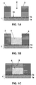
- Figures 1A to 1 F illustrate subsequent steps in a method according to embodiments of the present invention.
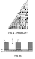
- Figure 2 illustrates suitable combinations for binary and ternary alloys which can be taken into account to perform co-deposition of catalytic material embedded in a non-catalytic matrix using electrodeposition (from D. Landolt et al. "Electrochemical and Materials Science Aspects of Alloy Deposition", Electrochimica Acta, Vol. 39, No. 8/9, 1075-1090, 1994 ).
- Figures 3A to 3E illustrate subsequent steps in a method according to embodiments of the invention.
- FIGS. 4A and 4B illustrate a possible application of a method according to embodiments of the invention.
- the present invention relates to a method for providing at least one catalyst nanoparticle on at least one sidewall of a three dimensional structure on a main surface of a substrate.
- the invention furthermore provides a method for forming at least one elongated nanostructure using the at least one nanoparticle as a catalyst.
- a method for providing at least one catalyst nanoparticle on at least one sidewall of a three-dimensional structure on a main surface of a substrate, the main surface lying in a plane and the sidewall of the three-dimensional structure lying in a plane substantially perpendicular to the plane of the main surface of the substrate.
- the method comprises:
- Catalyst nanoparticles formed by the method according to embodiments of the invention may advantageously be used as a catalyst for growing substantially parallel nanostructures at the at least one sidewall of the three-dimensional structures.
- These catalyst nanoparticles which can be located at predetermined locations, e.g. at the sidewalls, can catalyse the nucleation and growth of elongated nanostructures, such as e.g. carbon nanotubes (CNTs) or nanowires (NWs), using growth techniques such as Chemical Vapour Deposition (CVD), Vapour Liquid Solid (VLS) or Vapour Solid Solid (VSS) techniques.
- predetermined locations is meant here that, when so required, elongated nanostructures 9 can be formed only on the sidewalls 10 of the three-dimensional structures and nowhere else on the three-dimensional structure.
- the method for providing at least one catalyst nanoparticle on at least one sidewall of a three-dimensional structure on a substrate and the method for forming substantially parallel elongated nanostructures on a substrate according to embodiments of the invention can be used with any size of substrate and are fully compatible with semiconductor processing technology.
- elongated nanostructures any two-dimensionally confined pieces of solid material in the form of wires (nanowires), tubes (nanotubes), rods (nanorods) and similar elongated substantially cylindrical or polygonal nanostructures having a longitudinal axis.
- a cross-dimension of the elongated nanostructures preferably lies in the region of 1 to 500 nanometers.
- organic elongated nanostructures such as e.g. carbon nanotubes (CNTs), or inorganic elongated nanostructures, such as e.g. semiconducting nanowires (e.g. silicon nanowires) may be used.
- the term “base growth” of elongated nanostructures, such as e.g. CNTs or NWs, as used in this application refers to growth having the catalyst nanoparticle attached to the substrate.
- the term “tip growth” as used in this application refers to growth having the elongated nanostructures, such as e.g. CNTs or NWs, attached to a surface and the nanoparticle being on top of the elongated nanostructures, such as e.g. CNTs or NWs.
- catalyst nanoparticles refers to "active" catalyst nanoparticles which are suitable to be used as a catalyst for growth of elongated nanostructures, e.g. CNTs or NWs.
- active is to be understood as being capable of initiate growth/synthetization/creation of an elongated nanostructure, e.g. a CNT or NW.
- catalyst nanoparticle or catalytic nanoparticle it has to be understood that the same thing is meant, i.e. a nanoparticle that has properties to initiate the growth of elongated nanostructures such as CNTs or NWs.
- co-deposition means that two or more elements or particles are deposited at a same time, e.g. from a same bath, to respectively form an alloy or a composite.
- Different aspects and types of "co-deposition” are known in state of the art and described e.g. by Brenner et al. in “Electrodeposition of Alloys", Academic Press, New York, 1963.
- the term “substrate” may include any underlying material or “carrier” that may be used, or upon which a device, a circuit or an epitaxial layer may be formed.
- the “substrate” may comprise a carrier with a seed layer such as e.g. a WCN layer provided thereon.
- This seed layer acts as an electrode for subsequent electrochemical deposition (ECD) or for electroless deposition, also referred to as respectively electrochemical or electroless plating (see further).
- ECD electrochemical deposition
- electroless deposition also referred to as respectively electrochemical or electroless plating (see further).
- electrochemical deposition electrochemical deposition
- plating is meant an electrochemical process where an external electrical signal, e.g. current or voltage, is applied for reduction of metal ions.
- electroless deposition or “electroless plating” is meant an electrochemical process where a chemical reducing agent is used for reduction of the metal ions (and no external electrical signal such as current or voltage is applied).
- suitable carrier materials onto which seed layer material can be deposited are for example silicon, doped silicon, gallium arsenide (GaAs), gallium phosphide (GaP), gallium arsenide phosphide (GaAsP), indium phosphide (InP), germanium (Ge) or silicon germanium (SiGe).
- the "carrier” may further include an insulating layer such as a SiO 2 or an Si 3 N 4 layer underneath the seed layer.
- the substrate may be a substrate which itself has seed layer properties to initiate ECD or electroless deposition.
- a substrate 1 is provided.
- the substrate 1 should be such that it acts as a seed layer to initiate ECD or electroless deposition.
- the substrate 1 may comprise a carrier 1 a with at least one seed layer 1 b provided thereon (see Figure 1 A) .
- the at least one seed layer 1 b can be a continuous or discontinuous layer.
- the substrate 1 may be formed of a carrier 1 a onto which at least on seed layer 1b, for example a WCN layer, a Co layer or a copper layer, is provided such that a main surface of the substrate 1 can initiate ECD.
- At least one of the at least one seed layer 1 b should be continuous.
- two seed layers 1 b may be provided onto the carrier 1a. Therefore, for example, first a continuous WCN layer may be deposited followed by the deposition of a discontinuous Co layer.
- the substrate 1 in case of electroless deposition, may, for example, comprise a discontinuous deposited seed layer 1b comprising particles such as Pd, Pt or Ru to initiate electroless plating.
- the carrier 1 a may, for example, be e.g. a Si wafer or a Si/SiO 2 wafer.
- the substrate 1 may be formed of a bulk material which itself may have seed layer properties to initiate ECD or electroless deposition.
- additional provision of a seed layer 1 b may not be necessary but may, nevertheless, in some embodiments still be provided.
- a three-dimensional structure is formed. This may be accomplished by first providing a sacrificial pattern 3 onto the substrate 1.
- the sacrificial pattern 3 may comprise at least one opening or hole 2.
- the step of providing a sacrificial pattern 3 may be performed by first depositing a sacrificial layer and subsequently patterning at least one opening 2 in the sacrificial layer to form the sacrificial pattern 3 (see Figure 1A ).
- the openings 2 in the sacrificial layer may be formed using standard semiconductor processes, such as e.g. a combination of lithography and dry etching, e.g. anisotropic dry etching.
- Standard lithographic processing may at least comprise depositing at least one photosensitive layer, for example a photoresist layer, and optionally an antireflective coating on top of or underneath the sacrificial layer and developing the at least one photosensitive layer to create a photolithographic pattern.
- an antireflective coating is provided on top of the sacrificial layer, this coating may be so as to be easily removable during the lithography processing.
- the photolithographic pattern may then be used as a mask in e.g. reactive ion etching to form openings 2 in the sacrificial layer, thereby exposing parts of a main surface 15 of the substrate 1.
- the sacrificial layer can be a SiO 2 layer which may, for example, be formed by Chemical Vapour Deposition (CVD).
- the sacrificial layer may be an organic spin-on material such as, for example, commonly used polymer resist materials for lithography (e.g. PMMA (poly-methyl methacrylate)) or an organic low-k dielectric material such as e.g. SiLk ® .
- the thickness of the sacrificial layer depends on the application and on the size, more particularly height, of the three-dimensional structure to be formed, and may, for example, be in the range of between 10 nm and 10 ⁇ m.
- the substrate 1 may be immersed in an electrolytic bath to perform electrochemical co-deposition of a catalytic material and a non-catalytic material. This may, for example be done by ECD or alternatively by electroless deposition.
- the openings 2 are filled with a non-catalytic material 5 acting as matrix with embedded therein catalytic material.
- Figure 1 B illustrates the openings 2 which are filled with a co-deposit 4 of a non-catalytic material matrix having co-deposited catalytic material embedded therein.
- the openings 2 in the sacrificial layer may be partly filled. According to other embodiments of the invention, the openings 2 may also be completely filled.
- the non-catalytic and/or catalytic material may comprise a conductive material.
- the non-catalytic and/or catalytic material comprises a metal.
- electrochemical co-deposition of a first, non-catalytic material, e.g. metal, and a second, catalytic material, e.g. metal having standard potentials that are far apart can lead to a large difference in deposition rates of the two materials, e.g. metals.
- the catalytic and non-catalytic materials being metals, this would mean that a more noble metal would be deposited preferentially at low overpotentials.
- the co-deposition process may be performed at a potential suitable for depositing the non-catalytic material, e.g. metal, for the matrix.
- the standard potential of the second, catalytic material, e.g. metal may be far away from the potential at which deposition is performed, the deposition circumstances are not favourable for deposition of this second, catalytic material, e.g. metal, and thus only very small amounts of this catalytic material, e.g. metal, are deposited together with the first, non-catalytic material, e.g. metal.
- Details of co-deposition processes are described in " Electrochemical and Materials Science Aspects of Alloy Deposition", D. Landolt, Electrochimica Acta, Vol. 39, 1075-1090, 1994 and in A. Brenner, "Electrodeposition of alloys", Academic Press, new York, 1963 .
- Parameters of the co-deposition process such as bath composition and/or deposition potential may be tuned so that the amount of second, catalytic material that is deposited together with the matrix is such that it forms particles with a diameter of, for example, smaller than 5 nm, e.g. between 4 and 5 nm when single wall carbon nanotubes have to formed, with a diameter of between 5 nm and 30 nm when multi-wall carbon nanotubes have to be formed and with a diameter of larger than 30 nm when nanowires have to be formed.
- the non-catalytic matrix with embedded catalytic material made by co-deposition from an electrolyte solution with both the matrix and catalyst materials present as metal ions may also be referred to as an alloy.
- the alloy composition can be controlled by adjusting the bath composition (e.g. by changing the metal ion concentration), by adding complexing agents to bring the standard potentials closer together, and/or by using different deposition parameters (potential or current). By, for example, bringing the standard potentials closer together a better control of the deposition process, i.e. of the deposition rate, can be obtained and thus a better control of the composition of the deposited alloy can be obtained.
- the non-catalytic matrix with embedded catalytic material may be made by particle co-deposition from a solution that contains the matrix as metal ions and the catalyst material as nanoparticles.
- catalytic particles may be dispersed as metallic nanoparticles in solution and the matrix may be deposited from dissolved metal ions in the solution.
- a suitable solution to be used with the present embodiment may be Co nanoparticles in a cupric sulphate solution.
- the resulting co-deposit may in this case be referred to as composite.
- the composite composition or packing can be controlled by adjusting the bath composition from which the co-deposit is deposited, for example by changing the metal ion concentration, the volume fraction of the catalyst nanoparticles and/or the initial nanoparticle size. Details of particle co-deposition processes to form composites may be found in " Kinetics of particle co-deposition of nanocomposites", I. Shao et al., J. Electrochem. Soc. 149, C610, 2002 .
- Figure 2 illustrates some of the combinations of materials that are suitable to form binary and ternary alloys. These alloys can be taken into account to perform co-deposition of catalytic material embedded in a non-catalytic matrix by using electrodeposition ( D. Landolt et al. "Electrochemical and Materials Science Aspects of Alloy Deposition", Electrochimica Acta, Vol. 39, No. 8/9, 1075-1090, 1994 ). Black areas indicate alloys of particular importance. The crosses indicate other suitable alloys. The chemical components indicate a third alloy element added to form ternary alloys. Ternary alloys may, according to embodiments of the invention, comprise two catalytic and one non-catalytic material or may, according to other embodiments comprise one catalytic and two non-catalytic materials.
- the non-catalytic material to form the matrix may, for example, be copper, and the catalytic material may be cobalt, nickel, Iron, or any other suitable material which is able to initiate growth of elongated nanostructures, e.g. nanowires.
- a suitable combination which may be used with the method according to embodiments of the invention may, for example, be a copper matrix with embedded therein cobalt nanoparticles.
- a capping layer 6 may be provided, e.g. deposited on top of the co-deposited material 4.
- the capping layer 6 may, according to embodiments of the invention, be for preventing growth of elongated nanostructures on top of the three-dimensional structure.
- the thickness of the capping layer 6 may be in the range of a few nanometers up to several tens of nanometers.
- the capping layer 6 may be deposited by using electrochemical deposition (ECD) or, alternatively, by using electroless deposition.
- ECD electrochemical deposition
- the deposition of the capping layer 6 may be performed from the same electrolytic bath as the bath that is used for the provision of the co-deposit 4 (catalytic + non-catalytic material) for filling the openings 2 in the sacrificial layer, e.g. by adjusting the deposition potential, or, alternatively, may be deposited from a separate electrolytic bath.
- the capping layer 6 is deposited using sputter techniques such as Physical Vapour Deposition (PVD) or other deposition techniques such as Atomic Layer Deposition (ALD) or Chemical Vapour Deposition (CVD).
- PVD Physical Vapour Deposition
- ALD Atomic Layer Deposition
- CVD Chemical Vapour Deposition
- the material of the capping layer 6 may be deposited everywhere, including on the sacrificial pattern 3 and will have to be selectively removed by, for example, lift-off techniques, such that the capping layer 6 only remains on top of the co-deposit 4 in the openings 2 of the sacrificial pattern 3.
- the capping layer 6 may comprise one layer of material but may, alternatively, also comprise any number of layers.
- the capping layer 6 may comprise any suitable non-catalytic material that can be deposited by using ECD or electroless plating as long as it prevents the growth of elongated nanostructures on top of the three-dimensional structure.
- the material of the capping layer 6 may furthermore be such that it does not allow easy diffusion of the catalytic material from the non-catalytic matrix to the capping layer 6.
- the capping layer 6 may be formed of the same non-catalytic material as the material used to form the non-catalytic matrix.
- the capping layer 6 may be formed of a non-catalytic material that differs from the material used to form the non-catalytic matrix.
- the non-catalytic material of the capping layer 6 may be molybdenum and the material of the non-catalytic matrix may be copper.
- the capping layer 6 may be formed by a layer comprising copper.
- the non-catalytic matrix may comprise copper as well.
- Parameters of the co-deposition process may be tuned such that the catalytic material forms catalyst nanoparticles 7 in the non-catalytic matrix 5 with a diameter of, for example, below 5 nm, e.g. between 1 and 5 nm when single wall carbon nanotubes have to formed, with a diameter of between 5 nm and 30 nm when multi-wall carbon nanotubes or nanowires have to be formed and with a diameter of larger than 30 nm when carbon nanofibres or nanowires have to be formed.
- a co-deposit 4 may be formed which does not yet comprise suitable catalyst nanoparticles 7 for, for example, growing elongated nanostructures (see Figure 1 C) .
- the particles may have diameters which are too small or too large.
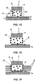
- an anneal step may be required such that catalytic material present in the co-deposit 4 is transformed into suitable catalytic nanoparticles 7 which are embedded in the non-catalytic matrix 5 (see Figure 1 D) .
- the anneal step may be performed before or after provision of the capping layer 6.
- annealing may be performed by, for example, a Rapid Thermal Anneal (RTA) at a temperature in the range of between 350°C and 900°C, preferably below 600°C.
- RTA Rapid Thermal Anneal
- annealing may be performed before the capping layer 6 is provided.
- the temperature at which annealing is performed may depend on the thickness d 2 (indicated in Figure 1 D) of the co-deposit 4.
- the thickness d 2 as well as the temperature and time duration of the annealing step may have an influence on the size and more particularly the diameter of the nanoparticles 7 formed.
- the concentration of the catalytic material and the properties of non-catalytic matrix itself may have an effect on the resulting nanoparticle size.
- Annealing may be performed for a time period of at least 10 seconds up to a few minutes. Annealing may be performed under an inert (N 2 or Ar) or reducing (containing H 2 or NH 3 ) atmosphere.
- the annealing step may also be performed after the step of depositing a capping layer 6.
- the sacrificial pattern 3 may be removed to expose sidewalls 10 of the non-catalytic matrix 5 to form the three-dimensional structure.
- the sidewalls 10 of the three-dimensional structure are, when a main surface 15 of the substrate 1 is lying in a plane, lying in a plane which is substantially perpendicular to the plane of the main surface 15 of the substrate 1.
- the method may furthermore comprise removing the exposed parts of the seed layer 1b, or in other words, parts of the seed layer 1 b which are not covered by the three-dimensional structure.
- the selective etch may be a wet etch using an etch solution which may comprise 3M NaOH (or KOH) and 1 g/l BTA (benzotriazole).
- the step of removing the sacrificial pattern 3 may be performed before the step of performing an anneal step to transform the catalytic material present in the co-deposit 4 into suitable catalytic nanoparticles 7 which are embedded in the non-catalytic matrix 5.
- part of the non-catalytic material 5 at the sidewalls 10 of the three-dimensional structure is selectively removed, for example by selective wet or dry etching, to expose at least part of at least one catalytic nanoparticle 7.
- copper at the sidewalls 10 of the three-dimensional structure may be removed by using an etch solution comprising an NH 4 OH/H 2 O 2 etchant and may, for example, be performed by using a solution comprising 25 mL NH 4 OH, 25 mL H 2 O and 50 mL 30% H 2 O 2 .
- Another suitable etchant to remove copper from the sidewalls 11 of the three-dimensional structure may be a solution of 2 vol% HNO 3 in water.
- Figure 1 E illustrates the three-dimensional structure having catalytic nanoparticles 8 exposed on its sidewalls 10.
- an additional cleaning step such as e.g. a wet cleaning step, may be performed to remove impurities which may be present on the exposed catalytic nanoparticles 8.
- impurities may be residues from processes used to, for example, remove the sacrificial layer or to remove part of the non-catalytic material.
- substantially impurity-free catalytic nanoparticles 8 may be obtained at the sidewalls 10 of the three-dimensional structures, which may then advantageously be used as a catalyst for, for example, growth of elongated nanostructures onto the sidewalls 10.
- the required diameter of the catalytic nanoparticles 8 to be formed may depend on the application.
- the catalyst nanoparticles 8 formed by the method according to embodiments of the invention may have a diameter of smaller than 100 nm.
- these nanoparticles 8 may have a diameter smaller than 5 nm, for example in the range between 1 nm and 5 nm.
- these nanoparticles 8 may have a diameter larger than 5 nm and preferably in the range of between 5 nm and 30 nm.
- removing exposed parts of the seed layer 1 b may be performed after removing part of the non-catalytic material 5 on the sidewalls 10 of the three-dimensional structure to expose the catalytic nanoparticles 8.
- the steps of removing exposed parts of the seed layer 1 b and removing part of the non-catalytic material 5 on the sidewalls 10 may be performed simultaneously; for example with a same etch chemistry, i.e. by using a same etch solution.
- the exposed catalytic nanoparticles 8 formed at the sidewalls 10 of a three-dimensional structure may advantageously be used for growing elongated nanostructures 9 such as CNTs or NWs lying in a plane substantially parallel to plane of the main surface 15 of the substrate 1 as illustrated in Figure 1 F .
- the present invention also provides a method for forming elongated nanostructures 9 using the exposed catalytic nanoparticles 8 on the sidewalls 10 of a three-dimensional structure as a catalyst.
- the method comprises providing catalyst nanoparticles 8 at at least one sidewall 10 of a three-dimensional structure on a substrate 1 as described hereabove in embodiments of the present invention and subsequently growing elongated nanostructures 9 using the exposed catalyst nanoparticles 8 as a catalyst, as will be explained hereafter.
- An advantage of the method for forming elongated nanostructures 9 according to embodiments of the invention is that it can be performed on any size of substrate. Furthermore, it is fully compatible with existing semiconductor processing, for example for manufacturing nanodevices.
- the method for forming elongated nanostructures 9 allows forming elongated nanostructures 9 with predetermined diameter and length and with a predetermined density.
- the density of the elongated nanostructures 9 formed may depend on the amount or concentration of catalytic material present in the co-deposit 4.
- a further advantage of the method for forming elongated nanostructures 9 according to embodiments of the invention is that it is possible to provide elongated nanostructures 9 at a predetermined location, e.g. on the sidewalls 10, of the three-dimensional structures.
- predetermined locations is meant here that, when required so, elongated nanostructures 9 can be formed only on the sidewalls 10 of the three-dimensional structures and nowhere else on the three-dimensional structure.
- the elongated nanostructures 9 formed may be substantially parallel elongated nanostructures 9.
- substantially parallel elongated nanostructures 9 is meant that, when the elongated nanostructures 9 have a longitudinal axis, the longitudinal axis of the elongated nanostructures 9 are lying in substantially parallel planes. Furthermore, the longitudinal axis of the elongated nanostructures 9 formed may be lying in a plane substantially parallel to the plane of the main surface 15 of the substrate 1 the three-dimensional structures are formed on.
- Figure 1 F illustrates the growth of parallel elongated nanostructures 9 using as a catalyst the exposed nanoparticles 8 formed at the sidewall 10 of a three-dimensional structure according to embodiments of the present invention. This may be done by exposing the nanoparticles 8 to proper synthesis conditions by using suitable techniques known by a person skilled in the art such as, for example, chemical vapour deposition (CVD), Vapour Liquid Solid (VLS) or Vapour Solid Solid (VSS) techniques.
- CVD chemical vapour deposition
- VLS Vapour Liquid Solid
- VLS Vapour Solid Solid
- growing elongated nanostructures may comprise growing carbon nanotubes (CNTs).
- growing the CNTs may comprise providing a carbon source and a carrier gas, and heating the substrate 1.
- the CNTs 9 may be grown by Chemical Vapor Deposition (CVD) or Plasma Enhanced-CVD (PE-CVD). These methods use a carbon source such as e.g. CH 4 , C 2 H 4 and C 2 H 2 and gases such as N 2 and/or H 2 as assistant gases.
- CVD Chemical Vapor Deposition
- PE-CVD Plasma Enhanced-CVD
- a carbon source such as e.g. CH 4 , C 2 H 4 and C 2 H 2 and gases
- gases such as N 2 and/or H 2 as assistant gases.
- growing CNTs 9 may be performed by using CH 4 as a carbon source and gases such as N 2 and/or H 2 as assistant gases and may be performed at growth temperatures lower than 900°C.
- other carbon sources may be used, such as C 2 H 4 , and other growth temperatures may be required.
- the growth temperature may be lower than 450°C to avoid damage to material of the substrate 1 on which the CNTs, or in general the elongated nanostructures 9, are grown.
- growth temperatures lower than 500°C may also be suitable for growing CNTs 9, or in general the elongated nanostructures 9.
- the diameter of the formed CNTs, or in general the elongated nanostructures 9 may be consistent with, i.e. may be substantially the same as, the diameter of the original catalyst nanoparticles 8 from which growth was started. With decreasing nanoparticle sizes, the diameter of the CNTs, or in general the elongated nanostructures 9 may become smaller, following a one to one relation.
- catalyst nanoparticles 8 formed by the method according to embodiments of the invention for growing elongated nanostructures 9 growth may occur through base growth or through tip growth, depending on the kind of catalyst nanoparticles 8 formed.
- the elongated nanostructures 9 may be grown in between neighbouring three-dimensional structures, i.e. they may be grown from a sidewall 10 of one three-dimensional structure to a sidewall 10 of another three-dimensional structure.
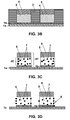
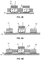
- Figures 3A to 3E illustrate a method for growing elongated nanostructures 9 parallel to a main surface of the substrate 1 from a sidewall 10 of a three-dimensional structure to an opposite sidewall of a neighbouring three-dimensional structure, according to embodiments of the present invention.
- a substrate 1 is provided which may comprise a carrier 1 a and a seed layer 1b for initiating ECD or electroless deposition.
- a substrate 1 may be provided which comprises seed layer properties for initiating ECD or electroless deposition itself.
- a sacrificial pattern 3 is formed on the substrate 1 (see Figure 3A ) by depositing a sacrificial layer onto the substrate 1 and subsequently forming openings 2 in the sacrificial layer 3 by patterning it. This may be done similar to the process described with respect to Figure 1A .
- the openings 2 are filled with a co-deposit 4 comprising a non-catalytic matrix with embedded therein a catalytic material as described with respect to Figure 1 B .
- a capping layer 6 may then be provided on top of the co-deposit 4 (see Figure 3B ).
- the patterned sacrificial layer 3 may be removed to form three-dimensional structures having sidewalls 10 which are lying in a plane substantially parallel to the plane of the main surface 15 of the substrate 1.
- an annealing step may be performed to form nanoparticles 7 in the non-catalytic matrix 5 (see Figure 3C ). The annealing step may be performed before or after removing the sacrificial layer 3.
- Elongated nanostructures 9 may then be grown in between neighbouring three-dimensional structures (see Fig. 3E ). Elongated nanostructures 9 may be grown by using any suitable method known by a person skilled in the art as described above.
- FIG. 4A and 4B illustrate a possible application for the method according to embodiments of the present invention.
- elongated nanostructures 9 such as e.g. CNTs or NWs may be grown substantially parallel to the plane of the main surface 15 of the substrate 1 from one sidewall 10 of a three-dimensional structure comprising catalyst nanoparticles 8 obtained according to embodiments of the present invention towards a sidewall of a "receiving" terminal 11, 12, e.g. a receiving three-dimensional structure, wherein the receiving structure is made of a different material than the three-dimensional structure the elongated nanostructures 9 are growing from and does not comprise catalyst nanoparticles 8.
- the receiving terminals 11, 12 may be another three-dimensional structure, a thin film, a metal, e.g.
- the receiving terminals 11, 12 In between the receiving terminals 11, 12 and the three-dimensional structure from which the nanostructures 9 are grown, there may be a distance of between 1 ⁇ m and 10 ⁇ m or between 1 ⁇ m and 100 ⁇ m. Additionally, according to other embodiments of the invention, trench or groove structures (not shown in the figures) may be provided at the sidewalls 10 of the three-dimensional structures to "guide" the growing CNTs from a nanoparticle 8 towards the receiving terminals 11 and 12.
- One possible approach for the fabrication of the receiving three-dimensional structures 11, 12 could be to apply a double lithographic step, where a through-mask deposition of the receiving terminals 11, 12 is performed first. Processing of a three-dimensional structure having catalytic nanoparticles 8 exposed at the sidewalls 10 may be performed according to the method of embodiments of the present invention as described above (see Figure 4A ).
- Elongated nanostructures 9 may then be grown in between the three-dimensional structure and the receiving terminals 11, 12 by a method as known by a person skilled in the art and as described above, thereby using the exposed catalyst nanoparticles 8 at the sidewalls 10 of the three-dimensional structure as a catalyst.
- the method according to embodiments of the invention for growing parallel nanostructures 9 based on the method for forming at least one catalytic nanoparticle 8 at at least one sidewall 10 of a three-dimensional structure according to embodiments of the invention can, for example, be used in the manufacturing process of semiconductor devices.
- the methods according to embodiments of the invention can be used to form interconnects in semiconductor devices.
Abstract
Description
- The present invention relates to formation of catalyst nanoparticles. More particularly, the present invention provides a method for providing at least one catalyst nanoparticle on at least one sidewall of a three-dimensional structure. The present invention also provides a method for forming at least one elongated nanostructure on at least one sidewall of a three-dimensional structure using such a catalyst nanoparticle as a catalyst.
- Nanostructures such as Nanowires (NWs) and Carbon Nanotubes (CNTs) have been identified as one of the most promising candidates to extend and even replace materials currently used in microelectronic manufacturing processes. For example, metallic CNTs have been proposed as nano-electronic interconnects due to their high current carrying capacity, whereas semiconducting CNTs have been indicated as nanoscale transistor elements due to their large range band gap. These and similar applications cannot be fully accomplished yet since the fabrication of nanostructures still faces a variety of unsolved issues, which vary from one application to another but may, however, be similar in some aspects.
- A first issue is related to the growth of nanostructures in a direction substantially parallel to a main surface of a substrate, i.e. in a direction, when the main surface of the substrate is lying in a plane, substantially parallel to the plane of the main substrate.
- It would be advantageous to form catalytic nanoparticles on sidewalls of e.g. vias and/or trenches and/or any desired three-dimensional structure, and then grow nanostructures directly from these catalytic nanoparticles and thus having e.g. CNT "interconnects" already in place, instead of going through a difficult task of placing them in the desired position in a separate step. In prior art methods, placement of catalyst particles on sidewalls of three-dimensional structures is described using physical vapor deposition or chemical vapour deposition (PVD or CVD) techniques. The samples on which CNTs have to be grown are therefore placed in a reactor such that CNTs grow parallel to the wafer surface.
- In "Advanced Materials, Vol. 15, No. 13, page 1105, 2003", Cao et al. describe direction-selective in-plane growth of CNTs between pre-patterned electrodes using chemical vapour deposition techniques. This technique is however based on a shadowing effect and deposition occurs only on sidewalls which all face the same direction. Hence, with this method, CNTs can only be grow into one, predetermined direction. Hence, this technique is not suitable for, for example, interconnect applications where the connections need to go in all possible directions in a plane substantially parallel to a main surface of a substrate.
- In "Applied Physics Letters, 89, 083105, 2006", Shi et al. describe direct synthesis of single-walled CNTs by bridging metal electrodes by laser-assisted chemical vapour deposition (LCVD). However, this synthesis is very localized and restricted by the size of a laser spot used. By using this technique, only a few CNTs are created across the electrodes (
Fig. 2 in this document only shows two CNTs formed on the substrate). Forming more CNTs, or in other words providing a higher density of CNTs on the substrate would be very cost-and time-ineffective because for this purpose the laser spot would have to be moved over the whole surface of the substrate. This technique is thus not well suited to obtain a high density of CNTs or NWs, e.g. a density of higher than 1012 cm-2, needed for interconnect applications. The technique is therefore not suitable for being used for mass production of CNTs. - Another issue is that the existing methods of manufacturing the above-mentioned nanostructures are not particularly compatible with standard, existing semiconductor processing techniques.
- In "Advanced Materials, Vol. 12, No. 12, page 890, 2000", Franklin et al. describe an enhanced CVD approach for extensive nanotube networks with directionality. With directionality is meant here, growing nanotubes having their longitudinal axis in a predetermined direction. However, in this approach use is made of silicon towers that are 10 µm high and it is difficult to make the method compatible with or to incorporate it in state of the art semiconductor processing.
- Despite the improvements achieved up till now, selective placement of catalytic nanoparticles onto sidewalls of three-dimensional structures remains critical to obtain subsequent growth of nanostructures which may be oriented parallel to the substrate. Up till now no methods exists in such a way that they are scalable and fully compatible with existing semiconductor processing in an economical attractive and realistic way.
- It is an object of the present invention to provide a good method for providing at least one catalyst nanoparticle on at least one sidewall of a three-dimensional structure on a substrate and a good method for forming elongated nanostructures using such catalyst nanoparticles as a catalyst.
- The above objectives are accomplished by methods and devices according to the present invention.
- The methods according to embodiments of the invention are scalable and fully compatible with existing semiconductor processing.
- Furthermore, methods according to embodiments of the invention can allow the growth of elongated nanostructures such as CNTs with control over the diameter, number, density and length of the elongated nanostructures.
- The methods according to embodiments of the invention provide a way for placing catalytic nanoparticles on sidewalls of a three-dimensional structure and hence provide an alternative for state of the art techniques such as sputtering nanoparticles onto the sidewalls of existing three-dimensional structures, which may be difficult for e.g. narrow interconnect structures.
- In a first aspect of the invention, a method is provided for providing at least one catalyst nanoparticle on at least one sidewall of a three-dimensional structure on a main surface of a substrate, the main surface lying in a plane and the sidewall of the three-dimensional structure lying in a plane substantially perpendicular to the plane of the main surface of the substrate. The method comprises:
- obtaining a three-dimensional structure on the main surface of the substrate, the three-dimensional structure comprising catalyst nanoparticles embedded in a non-catalytic matrix, and
- selectively removing at least part of the non-catalytic matrix at the sidewalls of the three-dimensional structure, to thereby expose at least one catalyst nanoparticle.
- Selectively removing at least part of the non-catalytic matrix at the sidewalls may be performed using wet etching and/or dry etching techniques.
- Obtaining a three-dimensional structure may be performed by:
- providing a sacrificial pattern on the main surface of the substrate, the sacrificial pattern comprising at least one opening,
- filling the at least one opening with a material comprising a non-catalytic matrix with embedded therein catalyst nanoparticles, and
- removing the sacrificial pattern to form the three-dimensional structure.
- Removing the sacrificial pattern may be done by wet etching or dry etching techniques.
- Filling the at least one opening with a material comprising a non-catalytic matrix with embedded therein catalyst nanoparticles may comprise:
- filling the at least one opening with a material comprising a non-catalytic matrix with embedded therein a catalytic material, and
- performing an annealing step to form the catalyst nanoparticles.
- The catalytic material embedded in a non-catalytic conductive matrix may be an alloy, for example may be an alloy of cobalt (Co) embedded in a copper (Cu) matrix.
- The annealing step may be performed by a Rapid Thermal Anneal at a temperature between 350°C and 900°C.
- Filling the at least one opening in the sacrificial pattern with a material comprising a non-catalytic matrix with embedded therein a catalytic material may be performed by co-deposition techniques. According to embodiments of the invention, the co-deposition technique may comprise alloy co-deposition in which both the catalytic material, e.g. metal, and non-catalytic material, e.g. metal, may be deposited from dissolved metal ions in an electrolyte. According to other embodiments of the invention, the co-deposition technique may comprise particle co-deposition in which catalytic nanoparticles are dispersed as metallic particles in a solution and the matrix is deposited from dissolved metal ions in the solution. For example, a suitable solution may comprise Co nanoparticles in a cupric sulphate solution.
- Filling the at least one opening with a material comprising a non-catalytic matrix with embedded therein a catalytic material may be performed by electrochemical deposition or by electroless deposition from a same electrolytic bath.
- Providing a sacrificial pattern may be performed by:
- providing a layer of sacrificial material, for example a layer of an organic material, onto the main surface of the substrate, and
- forming at least one opening in the layer of sacrificial material according to a predetermined pattern, thereby exposing a part of the main surface of the substrate.
- Forming at least one opening may be performed by patterning the sacrificial layer using photolithography and an anisotropic dry etch process to transfer the predetermined pattern to the sacrificial layer.
- According to embodiments of the invention the method may furthermore comprise providing a capping layer on top of the non-catalytic matrix before selectively removing at least part of the non-catalytic matrix at the sidewalls of the three-dimensional structure. The capping layer may be for preventing elongated nanostructure to be grown on the top of the three-dimensional structures.
- According to embodiments of the invention, the substrate may comprise a carrier, which may, for example be a semiconductor wafer, and a seed layer for initiating electrochemical deposition or electroless deposition. The seed layer may, for example, be a continuous or discontinuous layer comprising WCN or Cu or may, according to other embodiments, be a continuous or discontinuous layer comprising Pd, Pt and/or Ru particles.
- According to embodiments of the invention, the method may furthermore comprise, after removing the sacrificial pattern, removing exposed parts of the seed layer.
- In a further aspect of the invention, a method is provided for forming at least one elongated nanostructure on at least one sidewall of a three-dimensional structure on a main surface of a substrate, the main surface lying in a plane and the sidewall of the three-dimensional structure lying in a plane substantially perpendicular to the plane of the main surface of the substrate. The method comprises:
- obtaining a three-dimensional structure on the main surface, the three-dimensional structure comprising catalyst nanoparticles embedded in a non-catalytic matrix,
- selectively removing at least part of the non-catalytic matrix at the sidewalls of the three-dimensional structure to thereby expose at least one catalyst nanoparticle, and
- growing at least one elongated nanostructure using the at least one exposed catalyst nanoparticle as a catalyst.
- Growing at least one elongated nanostructure may be performed such that the at least one elongated nanostructure lies in a plane substantially parallel to the plane of the main surface of the substrate.
- Growing at least one elongated nanostructure may be performed by chemical vapour deposition, Vapour Liquid Solid or Vapour Solid Solid.
- According to embodiments of the invention, the elongated nanostructure may be a carbon nanotube (CNT), and growing the CNT may be performed by chemical vapour deposition using a carbon source.
- According to embodiments of the invention, the method may furthermore comprise providing a capping layer on top of the non-catalytic matrix before selectively removing at least part of the non-catalytic matrix at the sidewalls of the three-dimensional structure. The capping layer may be for preventing elongated nanostructure to be grown on the top of the three-dimensional structures.
- In a further aspect, a three-dimensional structure on a main surface of a substrate is provided, the three-dimensional structure comprising at least one elongated nanostructure on at least one sidewall thereof, the three-dimensional structure being obtained by a method according to embodiments of the present invention.
- The present invention provides in a further aspect, the use of the methods according to embodiments of the present invention in the manufacturing process of semiconductor devices.
- The present invention also provides the use of the methods according to embodiments of the present invention in the formation of interconnects in a semiconductor device.
- In yet a further aspect, the invention provides a semiconductor device comprising at least one three-dimensional structure on a main surface of a substrate, the main surface lying in a plane. The semiconductor device furthermore comprises at least one elongated nanostructure formed on at least one sidewall of the semiconductor device, the at least one elongated nanostructure lying in a plane substantially parallel to the plane of the main surface of the substrate and being formed by the methods according to embodiments of the present invention.
- According to embodiments of the invention, a method is provided for forming catalytic nanoparticles (catalysts) on at least one of the sidewalls of a vertical (3D) structure. The method according to this embodiment comprises at least the steps of:
- First providing a substrate with a sacrificial layer on top of said substrate, and
- Providing a sacrificial pattern having openings on said substrate and exposing the top surface of the substrate at the bottom of said openings, and
- At least partially filling said openings with catalytic material embedded in a non-catalytic matrix, and
- Providing a capping layer onto the non-catalytic matrix comprising catalytic material, and
- Removing the sacrificial layer to expose the sidewalls of the non-catalytic matrix to form the vertical (3D) structure, and
- Optionally, annealing the substrate such that the catalytic material is converted into catalytic nanoparticles, and
- Selectively etching (partly removing) the non-catalytic material on the sidewalls of the vertical (3D) structure to expose the nanoparticles.
- Particular and preferred aspects of the invention are set out in the accompanying independent and dependent claims. Features from the dependent claims may be combined with features of the independent claims and with features of other dependent claims as appropriate and not merely as explicitly set out in the claims.
- Although there has been constant improvement, change and evolution of devices in this field, the present concepts are believed to represent substantial new and novel improvements, including departures from prior practices, resulting in the provision of more efficient, stable and reliable devices of this nature.
- The above and other characteristics, features and advantages of the present invention will become apparent from the following detailed description, taken in conjunction with the accompanying drawings, which illustrate, by way of example, the principles of the invention. This description is given for the sake of example only, without limiting the scope of the invention. The reference figures quoted below refer to the attached drawings.
- All drawings are intended to illustrate some aspects and embodiments of the present invention. Not all alternatives and options are shown and therefore the invention is not limited to the content of the attached drawings. Like numerals are used to reference like parts in the different figures. The figures may show preferred embodiments.
-
Figures 1A to 1 F illustrate subsequent steps in a method according to embodiments of the present invention. -
Figure 2 illustrates suitable combinations for binary and ternary alloys which can be taken into account to perform co-deposition of catalytic material embedded in a non-catalytic matrix using electrodeposition (from D. Landolt et al. "Electrochemical and Materials Science Aspects of Alloy Deposition", Electrochimica Acta, Vol. 39, No. 8/9, 1075-1090, 1994). -
Figures 3A to 3E illustrate subsequent steps in a method according to embodiments of the invention. -
Figures 4A and 4B illustrate a possible application of a method according to embodiments of the invention. - In the different figures, the same reference signs refer to the same or analogous elements.
- The present invention will be described with respect to particular embodiments and with reference to certain drawings but the invention is not limited thereto but only by the claims. The drawings described are only schematic and are non-limiting. In the drawings, the size of some of the elements may be exaggerated and not drawn on scale for illustrative purposes. The dimensions and the relative dimensions do not correspond to actual reductions to practice of the invention.
- Moreover, the terms top, bottom and the like in the description and the claims are used for descriptive purposes and not necessarily for describing relative positions. It is to be understood that the terms so used are interchangeable under appropriate circumstances and that the embodiments of the invention described herein are capable of operation in other orientations than described or illustrated herein.
- It is to be noticed that the term "comprising", used in the claims, should not be interpreted as being restricted to the means listed thereafter; it does not exclude other elements or steps. It is thus to be interpreted as specifying the presence of the stated features, integers, steps or components as referred to, but does not preclude the presence or addition of one or more other features, integers, steps or components, or groups thereof. Thus, the scope of the expression "a device comprising means A and B" should not be limited to devices consisting only of components A and B. It means that with respect to the present invention, the only relevant components of the device are A and B.
- Reference throughout this specification to "one embodiment" or "an embodiment" means that a particular feature, structure or characteristic described in connection with the embodiment is included in at least one embodiment of the present invention. Thus, appearances of the phrases "in one embodiment" or "in an embodiment" in various places throughout this specification are not necessarily all referring to the same embodiment, but may. Furthermore, the particular features, structures or characteristics may be combined in any suitable manner, as would be apparent to one of ordinary skill in the art from this disclosure, in one or more embodiments.
- Similarly it should be appreciated that in the description of exemplary embodiments of the invention, various features of the invention are sometimes grouped together in a single embodiment, figure, or description thereof for the purpose of streamlining the disclosure and aiding in the understanding of one or more of the various inventive aspects. This method of disclosure, however, is not to be interpreted as reflecting an intention that the claimed invention requires more features than are expressly recited in each claim. Rather, as the following claims reflect, inventive aspects lie in less than all features of a single foregoing disclosed embodiment. Thus, the claims following the detailed description are hereby expressly incorporated into this detailed description, with each claim standing on its own as a separate embodiment of this invention.
- Furthermore, while some embodiments described herein include some but not other features included in other embodiments, combinations of features of different embodiments are meant to be within the scope of the invention, and form different embodiments, as would be understood by those in the art. For example, in the following claims, any of the claimed embodiments can be used in any combination.
- In the description provided herein, numerous specific details are set forth. However, it is understood that embodiments of the invention may be practiced without these specific details. In other instances, well-known methods, structures and techniques have not been shown in detail in order not to obscure an understanding of this description.
- The invention will be described by a detailed description of several embodiments of the invention. It is clear that other embodiments of the invention can be configured according to the knowledge of persons skilled in the art without departing from the true spirit or technical teaching of the invention, the invention being limited only by the terms of the appended claims.
- The present invention relates to a method for providing at least one catalyst nanoparticle on at least one sidewall of a three dimensional structure on a main surface of a substrate. The invention furthermore provides a method for forming at least one elongated nanostructure using the at least one nanoparticle as a catalyst.
- In one aspect of the invention, a method is provided for providing at least one catalyst nanoparticle on at least one sidewall of a three-dimensional structure on a main surface of a substrate, the main surface lying in a plane and the sidewall of the three-dimensional structure lying in a plane substantially perpendicular to the plane of the main surface of the substrate. The method comprises:
- obtaining a three-dimensional structure on the main surface of the substrate, the three-dimensional structure comprising catalyst nanoparticles embedded in a non-catalytic matrix , and
- selectively removing at least part of the non-catalytic matrix at the sidewalls of the three-dimensional structure to thereby expose at least one catalyst nanoparticle.
- Catalyst nanoparticles formed by the method according to embodiments of the invention may advantageously be used as a catalyst for growing substantially parallel nanostructures at the at least one sidewall of the three-dimensional structures. These catalyst nanoparticles, which can be located at predetermined locations, e.g. at the sidewalls, can catalyse the nucleation and growth of elongated nanostructures, such as e.g. carbon nanotubes (CNTs) or nanowires (NWs), using growth techniques such as Chemical Vapour Deposition (CVD), Vapour Liquid Solid (VLS) or Vapour Solid Solid (VSS) techniques. With predetermined locations is meant here that, when so required,
elongated nanostructures 9 can be formed only on thesidewalls 10 of the three-dimensional structures and nowhere else on the three-dimensional structure. - The method for providing at least one catalyst nanoparticle on at least one sidewall of a three-dimensional structure on a substrate and the method for forming substantially parallel elongated nanostructures on a substrate according to embodiments of the invention can be used with any size of substrate and are fully compatible with semiconductor processing technology.
- Hereinafter, the invention will be described by means of a detailed description of several embodiments. It is clear that other embodiments can be configured according to the knowledge of persons skilled in the art without departing from the true spirit or technical teaching of the invention, the invention being limited only by the terms of the appended claims.
- The following terms are provided solely to aid in the understanding of the invention.
- With the term elongated nanostructures is meant any two-dimensionally confined pieces of solid material in the form of wires (nanowires), tubes (nanotubes), rods (nanorods) and similar elongated substantially cylindrical or polygonal nanostructures having a longitudinal axis. A cross-dimension of the elongated nanostructures preferably lies in the region of 1 to 500 nanometers. According to embodiments of the present invention, organic elongated nanostructures, such as e.g. carbon nanotubes (CNTs), or inorganic elongated nanostructures, such as e.g. semiconducting nanowires (e.g. silicon nanowires) may be used.
- According to the invention, the term "base growth" of elongated nanostructures, such as e.g. CNTs or NWs, as used in this application refers to growth having the catalyst nanoparticle attached to the substrate. The term "tip growth" as used in this application refers to growth having the elongated nanostructures, such as e.g. CNTs or NWs, attached to a surface and the nanoparticle being on top of the elongated nanostructures, such as e.g. CNTs or NWs.
- The term "catalyst nanoparticles" refers to "active" catalyst nanoparticles which are suitable to be used as a catalyst for growth of elongated nanostructures, e.g. CNTs or NWs. In other words, "active" is to be understood as being capable of initiate growth/synthetization/creation of an elongated nanostructure, e.g. a CNT or NW. In the description, whenever the terms catalyst nanoparticle or catalytic nanoparticle are used, it has to be understood that the same thing is meant, i.e. a nanoparticle that has properties to initiate the growth of elongated nanostructures such as CNTs or NWs.
- According to the invention the term "co-deposition" means that two or more elements or particles are deposited at a same time, e.g. from a same bath, to respectively form an alloy or a composite. Different aspects and types of "co-deposition" are known in state of the art and described e.g. by Brenner et al. in "Electrodeposition of Alloys", Academic Press, New York, 1963.
- In embodiments of the present invention, the term "substrate" may include any underlying material or "carrier" that may be used, or upon which a device, a circuit or an epitaxial layer may be formed. According to embodiments of the invention, the "substrate" may comprise a carrier with a seed layer such as e.g. a WCN layer provided thereon. This seed layer acts as an electrode for subsequent electrochemical deposition (ECD) or for electroless deposition, also referred to as respectively electrochemical or electroless plating (see further). With "electrochemical deposition" or "plating" is meant an electrochemical process where an external electrical signal, e.g. current or voltage, is applied for reduction of metal ions. With "electroless deposition" or "electroless plating" is meant an electrochemical process where a chemical reducing agent is used for reduction of the metal ions (and no external electrical signal such as current or voltage is applied). Examples of suitable carrier materials onto which seed layer material can be deposited are for example silicon, doped silicon, gallium arsenide (GaAs), gallium phosphide (GaP), gallium arsenide phosphide (GaAsP), indium phosphide (InP), germanium (Ge) or silicon germanium (SiGe). According to alternative embodiments, the "carrier" may further include an insulating layer such as a SiO2 or an Si3N4 layer underneath the seed layer. According to further embodiments, the substrate may be a substrate which itself has seed layer properties to initiate ECD or electroless deposition.
- Subsequent steps in a method according to embodiments of the invention are schematically illustrated in
Figures 1A to 1 F . It has to be understood that this is only for the ease of explanation and that this is not intended to limit the invention in any way. The method may also comprise more or fewer steps or may comprise a different sequence of steps. - In a first step, a
substrate 1 is provided. According to embodiments of the invention, thesubstrate 1 should be such that it acts as a seed layer to initiate ECD or electroless deposition. Therefore, according to embodiments of the invention, thesubstrate 1 may comprise acarrier 1 a with at least oneseed layer 1 b provided thereon (seeFigure 1 A) . The at least oneseed layer 1 b can be a continuous or discontinuous layer. For example, in case of ECD deposition thesubstrate 1 may be formed of acarrier 1 a onto which at least onseed layer 1b, for example a WCN layer, a Co layer or a copper layer, is provided such that a main surface of thesubstrate 1 can initiate ECD. In case of ECD deposition at least one of the at least oneseed layer 1 b should be continuous. For example, according to a specific example, twoseed layers 1 b may be provided onto thecarrier 1a. Therefore, for example, first a continuous WCN layer may be deposited followed by the deposition of a discontinuous Co layer. According to other embodiments, in case of electroless deposition, thesubstrate 1 may, for example, comprise a discontinuous depositedseed layer 1b comprising particles such as Pd, Pt or Ru to initiate electroless plating. In both cases, i.e. in case of ECD and electroless deposition, thecarrier 1 a may, for example, be e.g. a Si wafer or a Si/SiO2 wafer. - Alternatively, the
substrate 1 may be formed of a bulk material which itself may have seed layer properties to initiate ECD or electroless deposition. In this case, additional provision of aseed layer 1 b may not be necessary but may, nevertheless, in some embodiments still be provided. - Onto the
substrate 1, a three-dimensional structure is formed. This may be accomplished by first providing asacrificial pattern 3 onto thesubstrate 1. Thesacrificial pattern 3 may comprise at least one opening orhole 2. According to embodiments of the invention, the step of providing asacrificial pattern 3 may be performed by first depositing a sacrificial layer and subsequently patterning at least oneopening 2 in the sacrificial layer to form the sacrificial pattern 3 (seeFigure 1A ). Theopenings 2 in the sacrificial layer may be formed using standard semiconductor processes, such as e.g. a combination of lithography and dry etching, e.g. anisotropic dry etching. Standard lithographic processing may at least comprise depositing at least one photosensitive layer, for example a photoresist layer, and optionally an antireflective coating on top of or underneath the sacrificial layer and developing the at least one photosensitive layer to create a photolithographic pattern. In case an antireflective coating is provided on top of the sacrificial layer, this coating may be so as to be easily removable during the lithography processing. The photolithographic pattern may then be used as a mask in e.g. reactive ion etching to formopenings 2 in the sacrificial layer, thereby exposing parts of amain surface 15 of thesubstrate 1. According to embodiments of the invention, the sacrificial layer can be a SiO2 layer which may, for example, be formed by Chemical Vapour Deposition (CVD). According to other embodiments of the invention, the sacrificial layer may be an organic spin-on material such as, for example, commonly used polymer resist materials for lithography (e.g. PMMA (poly-methyl methacrylate)) or an organic low-k dielectric material such as e.g. SiLk®. The thickness of the sacrificial layer depends on the application and on the size, more particularly height, of the three-dimensional structure to be formed, and may, for example, be in the range of between 10 nm and 10 µm. - After forming
openings 2 in the sacrificial layer thesubstrate 1 may be immersed in an electrolytic bath to perform electrochemical co-deposition of a catalytic material and a non-catalytic material. This may, for example be done by ECD or alternatively by electroless deposition. During the co-deposition process, theopenings 2 are filled with anon-catalytic material 5 acting as matrix with embedded therein catalytic material.Figure 1 B illustrates theopenings 2 which are filled with aco-deposit 4 of a non-catalytic material matrix having co-deposited catalytic material embedded therein. According to embodiments of the invention, and as illustrated inFigure 1 B , theopenings 2 in the sacrificial layer may be partly filled. According to other embodiments of the invention, theopenings 2 may also be completely filled. - The non-catalytic and/or catalytic material may comprise a conductive material. Preferably, the non-catalytic and/or catalytic material comprises a metal. As known by a person skilled in the art, electrochemical co-deposition of a first, non-catalytic material, e.g. metal, and a second, catalytic material, e.g. metal, having standard potentials that are far apart can lead to a large difference in deposition rates of the two materials, e.g. metals. In the case of a regular system, the catalytic and non-catalytic materials being metals, this would mean that a more noble metal would be deposited preferentially at low overpotentials. The co-deposition process may be performed at a potential suitable for depositing the non-catalytic material, e.g. metal, for the matrix. As the standard potential of the second, catalytic material, e.g. metal, may be far away from the potential at which deposition is performed, the deposition circumstances are not favourable for deposition of this second, catalytic material, e.g. metal, and thus only very small amounts of this catalytic material, e.g. metal, are deposited together with the first, non-catalytic material, e.g. metal. Details of co-deposition processes are described in "Electrochemical and Materials Science Aspects of Alloy Deposition", D. Landolt, Electrochimica Acta, Vol. 39, 1075-1090, 1994 and in A. Brenner, "Electrodeposition of alloys", Academic Press, new York, 1963.
- Parameters of the co-deposition process such as bath composition and/or deposition potential may be tuned so that the amount of second, catalytic material that is deposited together with the matrix is such that it forms particles with a diameter of, for example, smaller than 5 nm, e.g. between 4 and 5 nm when single wall carbon nanotubes have to formed, with a diameter of between 5 nm and 30 nm when multi-wall carbon nanotubes have to be formed and with a diameter of larger than 30 nm when nanowires have to be formed. This makes them suitable to be used as catalytic nanoparticles, from which for example elongated nanostructures may be grown.
- The non-catalytic matrix with embedded catalytic material made by co-deposition from an electrolyte solution with both the matrix and catalyst materials present as metal ions, may also be referred to as an alloy. The alloy composition can be controlled by adjusting the bath composition (e.g. by changing the metal ion concentration), by adding complexing agents to bring the standard potentials closer together, and/or by using different deposition parameters (potential or current). By, for example, bringing the standard potentials closer together a better control of the deposition process, i.e. of the deposition rate, can be obtained and thus a better control of the composition of the deposited alloy can be obtained.
- Alternatively, the non-catalytic matrix with embedded catalytic material may be made by particle co-deposition from a solution that contains the matrix as metal ions and the catalyst material as nanoparticles. Hence, according to these embodiments, catalytic particles may be dispersed as metallic nanoparticles in solution and the matrix may be deposited from dissolved metal ions in the solution. For example, a suitable solution to be used with the present embodiment may be Co nanoparticles in a cupric sulphate solution. The resulting co-deposit may in this case be referred to as composite. The composite composition or packing can be controlled by adjusting the bath composition from which the co-deposit is deposited, for example by changing the metal ion concentration, the volume fraction of the catalyst nanoparticles and/or the initial nanoparticle size. Details of particle co-deposition processes to form composites may be found in "Kinetics of particle co-deposition of nanocomposites", I. Shao et al., J. Electrochem. Soc. 149, C610, 2002.
-
Figure 2 illustrates some of the combinations of materials that are suitable to form binary and ternary alloys. These alloys can be taken into account to perform co-deposition of catalytic material embedded in a non-catalytic matrix by using electrodeposition (D. Landolt et al. "Electrochemical and Materials Science Aspects of Alloy Deposition", Electrochimica Acta, Vol. 39, No. 8/9, 1075-1090, 1994). Black areas indicate alloys of particular importance. The crosses indicate other suitable alloys. The chemical components indicate a third alloy element added to form ternary alloys. Ternary alloys may, according to embodiments of the invention, comprise two catalytic and one non-catalytic material or may, according to other embodiments comprise one catalytic and two non-catalytic materials. - According to embodiments of the invention, the non-catalytic material to form the matrix may, for example, be copper, and the catalytic material may be cobalt, nickel, Iron, or any other suitable material which is able to initiate growth of elongated nanostructures, e.g. nanowires. A suitable combination which may be used with the method according to embodiments of the invention may, for example, be a copper matrix with embedded therein cobalt nanoparticles.
- In a next step of a method according to embodiments of the present invention, which is illustrated in
Figure 1C , acapping layer 6 may be provided, e.g. deposited on top of theco-deposited material 4. Thecapping layer 6 may, according to embodiments of the invention, be for preventing growth of elongated nanostructures on top of the three-dimensional structure. However, when, according to other embodiments of the invention, the growth of elongated nanostructures on top of the three-dimensional structure is desired as well, nocapping layer 6 has to be provided. In particular embodiments, the thickness of thecapping layer 6 may be in the range of a few nanometers up to several tens of nanometers. Thecapping layer 6 may be deposited by using electrochemical deposition (ECD) or, alternatively, by using electroless deposition. The deposition of thecapping layer 6 may be performed from the same electrolytic bath as the bath that is used for the provision of the co-deposit 4 (catalytic + non-catalytic material) for filling theopenings 2 in the sacrificial layer, e.g. by adjusting the deposition potential, or, alternatively, may be deposited from a separate electrolytic bath. Alternatively, thecapping layer 6 is deposited using sputter techniques such as Physical Vapour Deposition (PVD) or other deposition techniques such as Atomic Layer Deposition (ALD) or Chemical Vapour Deposition (CVD). In the latter cases, the material of thecapping layer 6 may be deposited everywhere, including on thesacrificial pattern 3 and will have to be selectively removed by, for example, lift-off techniques, such that thecapping layer 6 only remains on top of the co-deposit 4 in theopenings 2 of thesacrificial pattern 3. Thecapping layer 6 may comprise one layer of material but may, alternatively, also comprise any number of layers. - According to embodiments of the invention, the
capping layer 6 may comprise any suitable non-catalytic material that can be deposited by using ECD or electroless plating as long as it prevents the growth of elongated nanostructures on top of the three-dimensional structure. The material of thecapping layer 6 may furthermore be such that it does not allow easy diffusion of the catalytic material from the non-catalytic matrix to thecapping layer 6. According to embodiments of the invention, thecapping layer 6 may be formed of the same non-catalytic material as the material used to form the non-catalytic matrix. According to other embodiments of the invention, thecapping layer 6 may be formed of a non-catalytic material that differs from the material used to form the non-catalytic matrix. For example, the non-catalytic material of thecapping layer 6 may be molybdenum and the material of the non-catalytic matrix may be copper. According to other embodiments of the invention, thecapping layer 6 may be formed by a layer comprising copper. The non-catalytic matrix may comprise copper as well. - Parameters of the co-deposition process may be tuned such that the catalytic material forms
catalyst nanoparticles 7 in thenon-catalytic matrix 5 with a diameter of, for example, below 5 nm, e.g. between 1 and 5 nm when single wall carbon nanotubes have to formed, with a diameter of between 5 nm and 30 nm when multi-wall carbon nanotubes or nanowires have to be formed and with a diameter of larger than 30 nm when carbon nanofibres or nanowires have to be formed. However, according to embodiments of the invention and as illustrated inFigures 1C and1D , aco-deposit 4 may be formed which does not yet comprisesuitable catalyst nanoparticles 7 for, for example, growing elongated nanostructures (seeFigure 1 C) . For example, the particles may have diameters which are too small or too large. In this case an anneal step may be required such that catalytic material present in theco-deposit 4 is transformed into suitablecatalytic nanoparticles 7 which are embedded in the non-catalytic matrix 5 (seeFigure 1 D) . The anneal step may be performed before or after provision of thecapping layer 6. - According to embodiments of the invention, annealing may be performed by, for example, a Rapid Thermal Anneal (RTA) at a temperature in the range of between 350°C and 900°C, preferably below 600°C. According to embodiments, annealing may be performed before the
capping layer 6 is provided. In that case, the temperature at which annealing is performed may depend on the thickness d2 (indicated inFigure 1 D) of theco-deposit 4. The thickness d2 as well as the temperature and time duration of the annealing step may have an influence on the size and more particularly the diameter of thenanoparticles 7 formed. Also the concentration of the catalytic material and the properties of non-catalytic matrix itself may have an effect on the resulting nanoparticle size. Annealing may be performed for a time period of at least 10 seconds up to a few minutes. Annealing may be performed under an inert (N2 or Ar) or reducing (containing H2 or NH3) atmosphere. - According to embodiments of the invention and depending on the nature of the
capping layer 6, the annealing step may also be performed after the step of depositing acapping layer 6. In that case, the thickness of the structure (= co-deposit 4 + capping layer 6) d1 (indicated inFigure 1 D) as well as the temperature and time duration of the annealing step may have an influence on controlling the size and more particularly the diameter of thenanoparticles 7. - In a next step, the
sacrificial pattern 3 may be removed to exposesidewalls 10 of thenon-catalytic matrix 5 to form the three-dimensional structure. Thesidewalls 10 of the three-dimensional structure are, when amain surface 15 of thesubstrate 1 is lying in a plane, lying in a plane which is substantially perpendicular to the plane of themain surface 15 of thesubstrate 1. By removing thesacrificial pattern 3 parts of themain surface 15 of thesubstrate 1, in the example given formed by theseed layer 1 b, may be exposed. Therefore, according to embodiments of the invention, the method may furthermore comprise removing the exposed parts of theseed layer 1b, or in other words, parts of theseed layer 1 b which are not covered by the three-dimensional structure. This may for example be done by a selective etch as known by a person skilled in the art. For example, in case theseed layer 1 b comprises a WCN layer (and the matrix is Cu), the selective etch may be a wet etch using an etch solution which may comprise 3M NaOH (or KOH) and 1 g/l BTA (benzotriazole). - According to alternative embodiments of the invention the step of removing the
sacrificial pattern 3 may be performed before the step of performing an anneal step to transform the catalytic material present in theco-deposit 4 into suitablecatalytic nanoparticles 7 which are embedded in thenon-catalytic matrix 5. - After the steps of depositing a
capping layer 6, performing an anneal step and removing the sacrificial pattern 3 (performed in any order), part of thenon-catalytic material 5 at thesidewalls 10 of the three-dimensional structure is selectively removed, for example by selective wet or dry etching, to expose at least part of at least onecatalytic nanoparticle 7. For example, in case thenon-catalytic material matrix 5 comprises copper and thecatalytic nanoparticles 7 embedded in thematrix 5 comprise cobalt, copper at thesidewalls 10 of the three-dimensional structure may be removed by using an etch solution comprising an NH4OH/H2O2 etchant and may, for example, be performed by using a solution comprising 25 mL NH4OH, 25 mL H2O and 50 mL 30% H2O2. Another suitable etchant to remove copper from thesidewalls 11 of the three-dimensional structure may be a solution of 2 vol% HNO3 in water.Figure 1 E illustrates the three-dimensional structure havingcatalytic nanoparticles 8 exposed on itssidewalls 10. - Optionally an additional cleaning step, such as e.g. a wet cleaning step, may be performed to remove impurities which may be present on the exposed
catalytic nanoparticles 8. These impurities may be residues from processes used to, for example, remove the sacrificial layer or to remove part of the non-catalytic material. In that way substantially impurity-freecatalytic nanoparticles 8 may be obtained at thesidewalls 10 of the three-dimensional structures, which may then advantageously be used as a catalyst for, for example, growth of elongated nanostructures onto thesidewalls 10. - The required diameter of the
catalytic nanoparticles 8 to be formed may depend on the application. Thecatalyst nanoparticles 8 formed by the method according to embodiments of the invention may have a diameter of smaller than 100 nm. According to specific embodiments, where, for example, single wall CNTs have to be formed using thecatalyst nanoparticles 8, thesenanoparticles 8 may have a diameter smaller than 5 nm, for example in the range between 1 nm and 5 nm. According to other specific embodiments, where multiwall CNTs have to be formed using thecatalyst nanoparticles 8, thesenanoparticles 8 may have a diameter larger than 5 nm and preferably in the range of between 5 nm and 30 nm. - According to alternative embodiments removing exposed parts of the
seed layer 1 b may be performed after removing part of thenon-catalytic material 5 on thesidewalls 10 of the three-dimensional structure to expose thecatalytic nanoparticles 8. Alternatively, the steps of removing exposed parts of theseed layer 1 b and removing part of thenon-catalytic material 5 on thesidewalls 10 may be performed simultaneously; for example with a same etch chemistry, i.e. by using a same etch solution. - According to embodiments of the present invention, the exposed
catalytic nanoparticles 8 formed at thesidewalls 10 of a three-dimensional structure may advantageously be used for growingelongated nanostructures 9 such as CNTs or NWs lying in a plane substantially parallel to plane of themain surface 15 of thesubstrate 1 as illustrated inFigure 1 F . - Therefore, the present invention also provides a method for forming
elongated nanostructures 9 using the exposedcatalytic nanoparticles 8 on thesidewalls 10 of a three-dimensional structure as a catalyst. The method comprises providingcatalyst nanoparticles 8 at at least onesidewall 10 of a three-dimensional structure on asubstrate 1 as described hereabove in embodiments of the present invention and subsequently growingelongated nanostructures 9 using the exposedcatalyst nanoparticles 8 as a catalyst, as will be explained hereafter. - An advantage of the method for forming
elongated nanostructures 9 according to embodiments of the invention is that it can be performed on any size of substrate. Furthermore, it is fully compatible with existing semiconductor processing, for example for manufacturing nanodevices. - Furthermore, the method for forming
elongated nanostructures 9 according to embodiments of the invention allows formingelongated nanostructures 9 with predetermined diameter and length and with a predetermined density. The density of theelongated nanostructures 9 formed may depend on the amount or concentration of catalytic material present in theco-deposit 4. - A further advantage of the method for forming
elongated nanostructures 9 according to embodiments of the invention is that it is possible to provideelongated nanostructures 9 at a predetermined location, e.g. on thesidewalls 10, of the three-dimensional structures. With predetermined locations is meant here that, when required so,elongated nanostructures 9 can be formed only on thesidewalls 10 of the three-dimensional structures and nowhere else on the three-dimensional structure. According to embodiments of the invention, theelongated nanostructures 9 formed may be substantially parallelelongated nanostructures 9. With substantially parallelelongated nanostructures 9 is meant that, when theelongated nanostructures 9 have a longitudinal axis, the longitudinal axis of theelongated nanostructures 9 are lying in substantially parallel planes. Furthermore, the longitudinal axis of theelongated nanostructures 9 formed may be lying in a plane substantially parallel to the plane of themain surface 15 of thesubstrate 1 the three-dimensional structures are formed on. -
Figure 1 F illustrates the growth of parallelelongated nanostructures 9 using as a catalyst the exposednanoparticles 8 formed at thesidewall 10 of a three-dimensional structure according to embodiments of the present invention. This may be done by exposing thenanoparticles 8 to proper synthesis conditions by using suitable techniques known by a person skilled in the art such as, for example, chemical vapour deposition (CVD), Vapour Liquid Solid (VLS) or Vapour Solid Solid (VSS) techniques. - According to specific embodiments of the invention, growing elongated nanostructures may comprise growing carbon nanotubes (CNTs). In this case, growing the CNTs may comprise providing a carbon source and a carrier gas, and heating the
substrate 1. - According to embodiments of the invention the
CNTs 9 may be grown by Chemical Vapor Deposition (CVD) or Plasma Enhanced-CVD (PE-CVD). These methods use a carbon source such as e.g. CH4, C2H4 and C2H2 and gases such as N2 and/or H2 as assistant gases. For example, growingCNTs 9 may be performed by using CH4 as a carbon source and gases such as N2 and/or H2 as assistant gases and may be performed at growth temperatures lower than 900°C. - According to other embodiments, other carbon sources may be used, such as C2H4, and other growth temperatures may be required. For example, the growth temperature may be lower than 450°C to avoid damage to material of the
substrate 1 on which the CNTs, or in general theelongated nanostructures 9, are grown. For example, using other carbon sources such as C2H2, growth temperatures lower than 500°C may also be suitable for growingCNTs 9, or in general theelongated nanostructures 9. In general, the diameter of the formed CNTs, or in general theelongated nanostructures 9 may be consistent with, i.e. may be substantially the same as, the diameter of theoriginal catalyst nanoparticles 8 from which growth was started. With decreasing nanoparticle sizes, the diameter of the CNTs, or in general theelongated nanostructures 9 may become smaller, following a one to one relation. - In general, by using the
catalyst nanoparticles 8 formed by the method according to embodiments of the invention for growingelongated nanostructures 9, growth may occur through base growth or through tip growth, depending on the kind ofcatalyst nanoparticles 8 formed. - According to embodiments of the invention, the
elongated nanostructures 9 may be grown in between neighbouring three-dimensional structures, i.e. they may be grown from asidewall 10 of one three-dimensional structure to asidewall 10 of another three-dimensional structure.Figures 3A to 3E illustrate a method for growingelongated nanostructures 9 parallel to a main surface of thesubstrate 1 from asidewall 10 of a three-dimensional structure to an opposite sidewall of a neighbouring three-dimensional structure, according to embodiments of the present invention. - The method may comprise similar process steps as described with respect to
Figure 1 A to 1 F . Asubstrate 1 is provided which may comprise acarrier 1 a and aseed layer 1b for initiating ECD or electroless deposition. According to other embodiments, asubstrate 1 may be provided which comprises seed layer properties for initiating ECD or electroless deposition itself. Then, asacrificial pattern 3 is formed on the substrate 1 (seeFigure 3A ) by depositing a sacrificial layer onto thesubstrate 1 and subsequently formingopenings 2 in thesacrificial layer 3 by patterning it. This may be done similar to the process described with respect toFigure 1A . Next, theopenings 2 are filled with aco-deposit 4 comprising a non-catalytic matrix with embedded therein a catalytic material as described with respect toFigure 1 B . Acapping layer 6 may then be provided on top of the co-deposit 4 (seeFigure 3B ). In a next step, the patternedsacrificial layer 3 may be removed to form three-dimensionalstructures having sidewalls 10 which are lying in a plane substantially parallel to the plane of themain surface 15 of thesubstrate 1. Optionally an annealing step may be performed to formnanoparticles 7 in the non-catalytic matrix 5 (seeFigure 3C ). The annealing step may be performed before or after removing thesacrificial layer 3. Then, part of thenon-catalytic matrix 5 is removed at thesidewalls 10 of the three-dimensional structures, thereby exposing at least part of at least one nanoparticle 8 (seeFigure 3D ).Elongated nanostructures 9 may then be grown in between neighbouring three-dimensional structures (seeFig. 3E ).Elongated nanostructures 9 may be grown by using any suitable method known by a person skilled in the art as described above. -
Figure 4A and 4B illustrate a possible application for the method according to embodiments of the present invention. In this application,elongated nanostructures 9 such as e.g. CNTs or NWs may be grown substantially parallel to the plane of themain surface 15 of thesubstrate 1 from onesidewall 10 of a three-dimensional structure comprisingcatalyst nanoparticles 8 obtained according to embodiments of the present invention towards a sidewall of a "receiving"terminal elongated nanostructures 9 are growing from and does not comprisecatalyst nanoparticles 8. The receivingterminals terminals nanostructures 9 are grown, there may be a distance of between 1 µm and 10 µm or between 1 µm and 100 µm. Additionally, according to other embodiments of the invention, trench or groove structures (not shown in the figures) may be provided at thesidewalls 10 of the three-dimensional structures to "guide" the growing CNTs from ananoparticle 8 towards the receivingterminals dimensional structures terminals catalytic nanoparticles 8 exposed at thesidewalls 10 may be performed according to the method of embodiments of the present invention as described above (seeFigure 4A ). -
Elongated nanostructures 9 may then be grown in between the three-dimensional structure and the receivingterminals catalyst nanoparticles 8 at thesidewalls 10 of the three-dimensional structure as a catalyst. - The method according to embodiments of the invention for growing
parallel nanostructures 9 based on the method for forming at least onecatalytic nanoparticle 8 at at least onesidewall 10 of a three-dimensional structure according to embodiments of the invention can, for example, be used in the manufacturing process of semiconductor devices. For example, the methods according to embodiments of the invention can be used to form interconnects in semiconductor devices. - It is to be understood that although preferred embodiments, specific constructions and configurations, as well as materials, have been discussed herein for devices according to the present invention, various changes or modifications in form and detail may be made without departing from the scope of this invention as defined by the appended claims.
Claims (22)
- Method for providing at least one catalyst nanoparticle (8) on at least one sidewall (10) of a three-dimensional structure on a main surface (15) of a substrate (1a, 1 b), the main surface (15) lying in a plane and the sidewall (10) of the three-dimensional structure lying in a plane substantially perpendicular to the plane of the main surface (15) of the substrate (1 a, 1 b), the method comprising:- obtaining a three-dimensional structure on the main surface (15), the three-dimensional structure comprising catalyst nanoparticles (7) embedded in a non-catalytic matrix (5) , and- selectively removing at least part of the non-catalytic matrix (5) at the sidewalls (10) of the three-dimensional structure to thereby expose at least one catalyst nanoparticle (8).
- Method according to claim 1, wherein obtaining a three-dimensional structure is performed by:- providing a sacrificial pattern (3) on the main surface (15) of the substrate (1a, 1b), the sacrificial pattern (3) comprising at least one opening (2),- filling the at least one opening (2) with a material comprising a non-catalytic matrix (5) with embedded therein catalyst nanoparticles (7), and- removing the sacrificial pattern (3) to form the three-dimensional structure.
- Method according to claim 2, wherein filling the at least one opening (2) with a material comprising a non-catalytic matrix (5) with embedded therein catalyst nanoparticles (7) comprises:- filling the at least one opening (2) with a material comprising a non-catalytic matrix with embedded therein a catalytic material, and- performing an annealing step to form the catalyst nanoparticles (7).
- Method according to claim 3, wherein the annealing step is performed by a Rapid Thermal Anneal at a temperature between 350°C and 900°C.
- Method according to any of claims 3 or 4, wherein filling the at least one opening (2) with a material comprising a non-catalytic matrix with embedded therein a catalytic material is performed by a co-deposition technique.
- Method according to claim 5, wherein filling the at least one opening (2) with a material comprising a non-catalytic matrix with embedded therein a catalytic material is performed by electrochemical deposition or by electroless deposition.
- Method according to any of claims 2 to 6, wherein providing a sacrificial pattern (3) is performed by:- providing a layer of sacrificial material onto the main surface (15) of the substrate (1a, 1 b), and- forming at least one opening (2) in the layer of sacrificial material according to a predetermined pattern, thereby exposing a part of the main surface (15) of the substrate (1a, 1b).
- Method according to claim 7, wherein providing a layer of sacrificial material is performed by providing a layer of organic material.
- Method according to claim 7 or 8, wherein forming at least one opening (2) is performed by patterning the sacrificial layer using photolithography and an anisotropic dry etch process to transfer the predetermined pattern to the sacrificial layer.
- Method according to any of the previous claims, furthermore comprising providing a capping layer (6) on top of the non-catalytic matrix (5) before selectively removing at least part of the non-catalytic matrix (5) at the sidewalls (10) of the three-dimensional structure.
- Method according to any of the previous claims, wherein the substrate comprises a carrier (1 a) and a seed layer (1 b) for initiating electrochemical deposition or electroless deposition.
- Method according to claim 11, wherein the carrier (1a) is a semiconductor wafer.
- Method according to claim 11 or 12, wherein the seed layer (1b) is a continuous or discontinuous layer comprising WCN or Cu.
- Method according to any of claims 11 to 13, wherein the seed layer (1 b) is a continuous or discontinuous layer comprising Pd, Pt and/or Ru particles.
- Method according to any of claims 11 to 14, wherein the method furthermore comprises, after removing the sacrificial pattern (3), removing exposed parts of the seed layer (1 b).
- Method for forming at least one elongated nanostructure (9) on at least one sidewall (10) of a three-dimensional structure on a main surface (15) of a substrate (1a, 1b), the main surface (15) lying in a plane and the sidewall (10) of the three-dimensional structure lying in a plane substantially perpendicular to the plane of the main surface (15) of the substrate (1a, 1 b), the method comprising:- obtaining a three-dimensional structure on the main surface (15) of the substrate, the three-dimensional structure comprising catalyst nanoparticles (7) embedded in a non-catalytic matrix (5),- selectively removing at least part of the non-catalytic matrix (5) at the sidewalls (10) of the three-dimensional structure to thereby expose at least one catalyst nanoparticle (8), and- growing at least one elongated nanostructure (9) using the at least one exposed catalyst nanoparticle (8) as a catalyst.
- Method according to claim 16, wherein growing at least one elongated nanostructure (9) is performed such that the at least one elongated nanostructure (9) lies in a plane substantially parallel to the plane of the main surface (15) of the substrate (1a, 1b).
- Method according to claim 16 or 17, wherein growing at least one elongated nanostructure (9) is performed by chemical vapour deposition, Vapour Liquid Solid or Vapour Solid Solid.
- Method according to any of claims 16 to 18, furthermore comprising providing a capping layer (6) on top of the non-catalytic matrix (5) before selectively removing at least part of the non-catalytic matrix (5) at the sidewalls (10) of the three-dimensional structure.
- Use of the method according to any of claims 1 to 19 in the manufacturing process of a semiconductor device.
- Use of the method according to any of claims 16 to 19 in the formation of interconnects in a semiconductor device.
- A semiconductor device comprising at least one three-dimensional structure on a main surface (15) of a substrate (1a, 1b), the main surface (15) lying in a plane, wherein the semiconductor device furthermore comprises at least one elongated nanostructure (9) formed on at least one sidewall (10) of the semiconductor device, the at least one elongated nanostructure (9) lying in a plane substantially parallel to the plane of the main surface (15) of the substrate (1a, 1b) and being formed by the method according to any of claims 16 to 19.
Priority Applications (2)
| Application Number | Priority Date | Filing Date | Title |
|---|---|---|---|
| US12/146,885 US7718531B2 (en) | 2007-07-06 | 2008-06-26 | Method for forming catalyst nanoparticles for growing elongated nanostructures |
| JP2008173401A JP5231105B2 (en) | 2007-07-06 | 2008-07-02 | Method of forming catalyst nanoparticles for growing elongated nanostructures |
Applications Claiming Priority (1)
| Application Number | Priority Date | Filing Date | Title |
|---|---|---|---|
| US94838207P | 2007-07-06 | 2007-07-06 |
Publications (3)
| Publication Number | Publication Date |
|---|---|
| EP2011572A2 true EP2011572A2 (en) | 2009-01-07 |
| EP2011572A3 EP2011572A3 (en) | 2009-05-20 |
| EP2011572B1 EP2011572B1 (en) | 2012-12-05 |
Family
ID=39941418
Family Applications (1)
| Application Number | Title | Priority Date | Filing Date |
|---|---|---|---|
| EP07075889A Not-in-force EP2011572B1 (en) | 2007-07-06 | 2007-10-16 | Method for forming catalyst nanoparticles for growing elongated nanostructures |
Country Status (3)
| Country | Link |
|---|---|
| US (1) | US7718531B2 (en) |
| EP (1) | EP2011572B1 (en) |
| JP (1) | JP5231105B2 (en) |
Cited By (1)
| Publication number | Priority date | Publication date | Assignee | Title |
|---|---|---|---|---|
| EP2402082A3 (en) * | 2010-06-29 | 2017-01-25 | Imec | Method for forming a catalyst suitable for growth of carbon nanotubes |
Families Citing this family (36)
| Publication number | Priority date | Publication date | Assignee | Title |
|---|---|---|---|---|
| US8951632B2 (en) * | 2007-01-03 | 2015-02-10 | Applied Nanostructured Solutions, Llc | CNT-infused carbon fiber materials and process therefor |
| US9005755B2 (en) | 2007-01-03 | 2015-04-14 | Applied Nanostructured Solutions, Llc | CNS-infused carbon nanomaterials and process therefor |
| US20100279569A1 (en) * | 2007-01-03 | 2010-11-04 | Lockheed Martin Corporation | Cnt-infused glass fiber materials and process therefor |
| US20120189846A1 (en) * | 2007-01-03 | 2012-07-26 | Lockheed Martin Corporation | Cnt-infused ceramic fiber materials and process therefor |
| US8158217B2 (en) * | 2007-01-03 | 2012-04-17 | Applied Nanostructured Solutions, Llc | CNT-infused fiber and method therefor |
| US8951631B2 (en) | 2007-01-03 | 2015-02-10 | Applied Nanostructured Solutions, Llc | CNT-infused metal fiber materials and process therefor |
| US8148188B2 (en) * | 2008-02-26 | 2012-04-03 | Imec | Photoelectrochemical cell with carbon nanotube-functionalized semiconductor electrode |
| US8668833B2 (en) * | 2008-05-21 | 2014-03-11 | Globalfoundries Singapore Pte. Ltd. | Method of forming a nanostructure |
| FR2933237B1 (en) * | 2008-06-25 | 2010-10-29 | Commissariat Energie Atomique | ARCHITECTURE OF HORIZONTAL INTERCONNECTIONS BASED ON CARBON NANOTUBES. |
| CN102317200B (en) * | 2009-02-17 | 2014-04-09 | 应用纳米结构方案公司 | Composites comprising carbon nanotubes on fiber |
| US20100227134A1 (en) | 2009-03-03 | 2010-09-09 | Lockheed Martin Corporation | Method for the prevention of nanoparticle agglomeration at high temperatures |
| US20100272891A1 (en) * | 2009-04-10 | 2010-10-28 | Lockheed Martin Corporation | Apparatus and method for the production of carbon nanotubes on a continuously moving substrate |
| CA2758568A1 (en) * | 2009-04-24 | 2010-10-28 | Applied Nanostructured Solutions, Llc | Cnt-infused emi shielding composite and coating |
| US9111658B2 (en) | 2009-04-24 | 2015-08-18 | Applied Nanostructured Solutions, Llc | CNS-shielded wires |
| US8664573B2 (en) * | 2009-04-27 | 2014-03-04 | Applied Nanostructured Solutions, Llc | CNT-based resistive heating for deicing composite structures |
| US20100279010A1 (en) * | 2009-04-30 | 2010-11-04 | Lockheed Martin Corporation | Method and system for close proximity catalysis for carbon nanotube synthesis |
| US20110123735A1 (en) * | 2009-11-23 | 2011-05-26 | Applied Nanostructured Solutions, Llc | Cnt-infused fibers in thermoset matrices |
| JP2013511655A (en) * | 2009-11-23 | 2013-04-04 | アプライド ナノストラクチャード ソリューションズ リミテッド ライアビリティー カンパニー | CNT-based land-based composite structure |
| JP2013511467A (en) * | 2009-11-23 | 2013-04-04 | アプライド ナノストラクチャード ソリューションズ リミテッド ライアビリティー カンパニー | CERAMIC COMPOSITE MATERIAL CONTAINING CARBON NANOTUBE LEATED FIBER MATERIAL AND PROCESS FOR PRODUCING THE SAME |
| EP2513250A4 (en) * | 2009-12-14 | 2015-05-27 | Applied Nanostructured Sols | Flame-resistant composite materials and articles containing carbon nanotube-infused fiber materials |
| US9167736B2 (en) * | 2010-01-15 | 2015-10-20 | Applied Nanostructured Solutions, Llc | CNT-infused fiber as a self shielding wire for enhanced power transmission line |
| CA2785803A1 (en) * | 2010-02-02 | 2011-11-24 | Applied Nanostructured Solutions, Llc | Carbon nanotube-infused fiber materials containing parallel-aligned carbon nanotubes, methods for production thereof, and composite materials derived therefrom |
| BR112012021634A2 (en) * | 2010-03-02 | 2019-09-24 | Applied Nanostructured Sols | electrical devices containing infused carbon nanotube fibers and methods for reproducing them. |
| BR112012021968A2 (en) | 2010-03-02 | 2016-06-07 | Applied Nanostructured Sols | spiral-wound electrical devices containing carbon nanotube-infused electrode materials and methods and apparatus for their production |
| US8780526B2 (en) | 2010-06-15 | 2014-07-15 | Applied Nanostructured Solutions, Llc | Electrical devices containing carbon nanotube-infused fibers and methods for production thereof |
| US8518826B2 (en) * | 2010-07-13 | 2013-08-27 | Lam Research Corporation | Metallization processes, mixtures, and electronic devices |
| US9017854B2 (en) | 2010-08-30 | 2015-04-28 | Applied Nanostructured Solutions, Llc | Structural energy storage assemblies and methods for production thereof |
| US20120058352A1 (en) * | 2010-09-02 | 2012-03-08 | Applied Nanostructured Solutions, Llc | Metal substrates having carbon nanotubes grown thereon and methods for production thereof |
| BR112012017246A2 (en) | 2010-09-23 | 2016-03-22 | Applied Nanostructured Solutins Llc | cnt infused fiber as a self-shielded wire for enhanced power transmission line |
| US9085464B2 (en) | 2012-03-07 | 2015-07-21 | Applied Nanostructured Solutions, Llc | Resistance measurement system and method of using the same |
| US9139416B2 (en) * | 2012-08-01 | 2015-09-22 | University Of South Carolina | Microfluidic devices for the generation of nano-vapor bubbles and their methods of manufacture and use |
| BR112015032647A2 (en) | 2013-06-28 | 2017-07-25 | Harvard College | structures coated with high surface area functional material |
| JP6181006B2 (en) * | 2014-07-09 | 2017-08-16 | 東京エレクトロン株式会社 | Plating pretreatment method, plating treatment system, and storage medium |
| JP2019513669A (en) | 2016-04-01 | 2019-05-30 | プレジデント アンド フェローズ オブ ハーバード カレッジ | Co-assembly to form high quality titania, alumina and other metal oxide template materials |
| CN109420516B (en) * | 2017-08-28 | 2021-08-06 | 广州中国科学院沈阳自动化研究所分所 | Platinum metal loaded carbon nitride film and preparation method and application thereof |
| CN111447995A (en) | 2017-09-29 | 2020-07-24 | 哈佛学院院长及董事 | Enhanced catalytic materials with partially embedded catalytic nanoparticles |
Family Cites Families (8)
| Publication number | Priority date | Publication date | Assignee | Title |
|---|---|---|---|---|
| DE19737752A1 (en) * | 1997-08-29 | 1999-03-04 | Egon Schmid | Electric motor |
| US6515339B2 (en) | 2000-07-18 | 2003-02-04 | Lg Electronics Inc. | Method of horizontally growing carbon nanotubes and field effect transistor using the carbon nanotubes grown by the method |
| JP3639808B2 (en) * | 2000-09-01 | 2005-04-20 | キヤノン株式会社 | Electron emitting device, electron source, image forming apparatus, and method of manufacturing electron emitting device |
| JP2003081622A (en) * | 2001-09-10 | 2003-03-19 | Sanyo Electric Co Ltd | Aggregate of carbon nanotube, and electronic element and electronic circuit obtained by using the same |
| WO2005025734A2 (en) * | 2003-09-17 | 2005-03-24 | Molecular Nanosystems, Inc. | Methods for producing and using catalytic substrates for carbon nanotube growth |
| JP4448356B2 (en) * | 2004-03-26 | 2010-04-07 | 富士通株式会社 | Semiconductor device and manufacturing method thereof |
| JP4213680B2 (en) * | 2004-08-31 | 2009-01-21 | 富士通株式会社 | Substrate structure and manufacturing method thereof, and semiconductor device and manufacturing method thereof |
| US7560769B2 (en) * | 2006-08-03 | 2009-07-14 | Micron Technology, Inc. | Non-volatile memory cell device and methods |
-
2007
- 2007-10-16 EP EP07075889A patent/EP2011572B1/en not_active Not-in-force
-
2008
- 2008-06-26 US US12/146,885 patent/US7718531B2/en not_active Expired - Fee Related
- 2008-07-02 JP JP2008173401A patent/JP5231105B2/en not_active Expired - Fee Related
Non-Patent Citations (8)
| Title |
|---|
| A. BRENNER: "Electrodeposition of alloys", 1963, ACADEMIC PRESS |
| BRENNER ET AL.: "Electrodeposition of Alloys", 1963, ACADEMIC PRESS, NEW YORK |
| CAO, ADVANCED MATERIALS, vol. 15, no. 13, pages 1105 |
| D. LANDOLT ET AL.: "Electrochemical and Materials Science Aspects of Alloy Deposition", ELECTROCHIMICA ACTA, vol. 39, no. 8/9, 1994, pages 1075 - 1090, XP002544201, DOI: doi:10.1016/0013-4686(94)E0022-R |
| D. LANDOLT: "Electrochemical and Materials Science Aspects of Alloy Deposition", ELECTROCHIMICA ACTA, vol. 39, 1994, pages 1075 - 1090, XP026528066, DOI: doi:10.1016/0013-4686(94)E0022-R |
| FRANKLIN, ADVANCED MATERIALS, vol. 12, no. 12, pages 890 |
| I. SHAO ET AL., J. ELECTROCHEM. SOC., vol. 149, 2002, pages C610 |
| SHI, APPLIED PHYSICS LETTERS, vol. 89, 2006, pages 083105 |
Cited By (1)
| Publication number | Priority date | Publication date | Assignee | Title |
|---|---|---|---|---|
| EP2402082A3 (en) * | 2010-06-29 | 2017-01-25 | Imec | Method for forming a catalyst suitable for growth of carbon nanotubes |
Also Published As
| Publication number | Publication date |
|---|---|
| EP2011572A3 (en) | 2009-05-20 |
| EP2011572B1 (en) | 2012-12-05 |
| US7718531B2 (en) | 2010-05-18 |
| JP5231105B2 (en) | 2013-07-10 |
| JP2009255025A (en) | 2009-11-05 |
| US20090072222A1 (en) | 2009-03-19 |
Similar Documents
| Publication | Publication Date | Title |
|---|---|---|
| US7718531B2 (en) | Method for forming catalyst nanoparticles for growing elongated nanostructures | |
| JP2009255025A6 (en) | Method of forming catalyst nanoparticles for growing elongated nanostructures | |
| Peng et al. | Metal‐particle‐induced, highly localized site‐specific etching of Si and formation of single‐crystalline Si nanowires in aqueous fluoride solution | |
| US8872154B2 (en) | Field effect transistor fabrication from carbon nanotubes | |
| US7250366B2 (en) | Carbon nanotubes with controlled diameter, length, and metallic contacts | |
| JP5329800B2 (en) | Control and selective formation of catalytic nanoparticles | |
| US11309388B2 (en) | Multi-super lattice for switchable arrays | |
| US20090197209A1 (en) | Lithographically patterned nanowire electrodeposition | |
| JP4208668B2 (en) | Semiconductor device and manufacturing method thereof | |
| JP5475339B2 (en) | Formation of single crystal semiconductor nanowires | |
| KR100834896B1 (en) | Semiconductor nano-structure, method for manufacturing thereof, and semiconductor device comprising the same | |
| Aca-López et al. | Effects of the doping level in the production of silicon nanowalls by metal assisted chemical etching | |
| US7183131B2 (en) | Process for producing a nanoelement arrangement, and nanoelement arrangement | |
| Djenizian et al. | Electrochemical fabrication of tin nanowires: a short review | |
| KR20130085880A (en) | Method of palladium nanowire hydrogen sensor using double eching and a sensor thereof | |
| US9691849B2 (en) | Ultra-long silicon nanostructures, and methods of forming and transferring the same | |
| KR100810983B1 (en) | Vertical Nanowire Growth Method at Selectve Locations, Semiconductor Nanodevice comprising Vertical Nanowire, and Fabrication Method thereof | |
| JP2012011374A (en) | Method for forming catalyst suitable for growth of carbon nanotube | |
| Chen et al. | Fabrication of ultrahigh-density nanowires by electrochemical nanolithography | |
| JP2008218615A (en) | Modified wiring forming method for integrated circuit | |
| Yasseri et al. | Electroless deposition of Au nanocrystals on Si (111) surfaces as catalysts for epitaxial growth of Si nanowires | |
| Lianto | Mechanism and catalyst stability of metal-assisted chemical etching of silicon | |
| Balasundaram | Metal-assisted chemical etching as a disruptive platform for multi-dimensional semiconductor sculpting | |
| US20140061935A1 (en) | Method for manufacturing a layer arrangement, and a layer arrangement | |
| Wang et al. | Highly selective electrodeposition of sub-10 nm crystalline noble metallic nanorods inside vertically aligned multiwall carbon nanotubes |
Legal Events
| Date | Code | Title | Description |
|---|---|---|---|
| PUAI | Public reference made under article 153(3) epc to a published international application that has entered the european phase |
Free format text: ORIGINAL CODE: 0009012 |
|
| AK | Designated contracting states |
Kind code of ref document: A2 Designated state(s): AT BE BG CH CY CZ DE DK EE ES FI FR GB GR HU IE IS IT LI LT LU LV MC MT NL PL PT RO SE SI SK TR |
|
| AX | Request for extension of the european patent |
Extension state: AL BA HR MK RS |
|
| PUAL | Search report despatched |
Free format text: ORIGINAL CODE: 0009013 |
|
| AK | Designated contracting states |
Kind code of ref document: A3 Designated state(s): AT BE BG CH CY CZ DE DK EE ES FI FR GB GR HU IE IS IT LI LT LU LV MC MT NL PL PT RO SE SI SK TR |
|
| AX | Request for extension of the european patent |
Extension state: AL BA HR MK RS |
|
| RAP1 | Party data changed (applicant data changed or rights of an application transferred) |
Owner name: IMEC |
|
| 17P | Request for examination filed |
Effective date: 20090918 |
|
| AKX | Designation fees paid |
Designated state(s): BE DE FR GB IT NL |
|
| RBV | Designated contracting states (corrected) |
Designated state(s): AT BE BG CH CY CZ DE DK EE ES FI FR GB GR HU IE IS IT LI LT LU LV MC MT NL PL PT RO SE SI SK TR |
|
| 17Q | First examination report despatched |
Effective date: 20110923 |
|
| GRAP | Despatch of communication of intention to grant a patent |
Free format text: ORIGINAL CODE: EPIDOSNIGR1 |
|
| GRAS | Grant fee paid |
Free format text: ORIGINAL CODE: EPIDOSNIGR3 |
|
| GRAA | (expected) grant |
Free format text: ORIGINAL CODE: 0009210 |
|
| AK | Designated contracting states |
Kind code of ref document: B1 Designated state(s): AT BE BG CH CY CZ DE DK EE ES FI FR GB GR HU IE IS IT LI LT LU LV MC MT NL PL PT RO SE SI SK TR |
|
| REG | Reference to a national code |
Ref country code: GB Ref legal event code: FG4D |
|
| REG | Reference to a national code |
Ref country code: CH Ref legal event code: EP |
|
| REG | Reference to a national code |
Ref country code: AT Ref legal event code: REF Ref document number: 586961 Country of ref document: AT Kind code of ref document: T Effective date: 20121215 |
|
| REG | Reference to a national code |
Ref country code: IE Ref legal event code: FG4D |
|
| REG | Reference to a national code |
Ref country code: DE Ref legal event code: R096 Ref document number: 602007027094 Country of ref document: DE Effective date: 20130131 |
|
| REG | Reference to a national code |
Ref country code: AT Ref legal event code: MK05 Ref document number: 586961 Country of ref document: AT Kind code of ref document: T Effective date: 20121205 |
|
| PG25 | Lapsed in a contracting state [announced via postgrant information from national office to epo] |
Ref country code: LT Free format text: LAPSE BECAUSE OF FAILURE TO SUBMIT A TRANSLATION OF THE DESCRIPTION OR TO PAY THE FEE WITHIN THE PRESCRIBED TIME-LIMIT Effective date: 20121205 Ref country code: SE Free format text: LAPSE BECAUSE OF FAILURE TO SUBMIT A TRANSLATION OF THE DESCRIPTION OR TO PAY THE FEE WITHIN THE PRESCRIBED TIME-LIMIT Effective date: 20121205 Ref country code: FI Free format text: LAPSE BECAUSE OF FAILURE TO SUBMIT A TRANSLATION OF THE DESCRIPTION OR TO PAY THE FEE WITHIN THE PRESCRIBED TIME-LIMIT Effective date: 20121205 Ref country code: ES Free format text: LAPSE BECAUSE OF FAILURE TO SUBMIT A TRANSLATION OF THE DESCRIPTION OR TO PAY THE FEE WITHIN THE PRESCRIBED TIME-LIMIT Effective date: 20130316 |
|
| REG | Reference to a national code |
Ref country code: NL Ref legal event code: VDEP Effective date: 20121205 |
|
| REG | Reference to a national code |
Ref country code: LT Ref legal event code: MG4D |
|
| PG25 | Lapsed in a contracting state [announced via postgrant information from national office to epo] |
Ref country code: PL Free format text: LAPSE BECAUSE OF FAILURE TO SUBMIT A TRANSLATION OF THE DESCRIPTION OR TO PAY THE FEE WITHIN THE PRESCRIBED TIME-LIMIT Effective date: 20121205 Ref country code: LV Free format text: LAPSE BECAUSE OF FAILURE TO SUBMIT A TRANSLATION OF THE DESCRIPTION OR TO PAY THE FEE WITHIN THE PRESCRIBED TIME-LIMIT Effective date: 20121205 Ref country code: GR Free format text: LAPSE BECAUSE OF FAILURE TO SUBMIT A TRANSLATION OF THE DESCRIPTION OR TO PAY THE FEE WITHIN THE PRESCRIBED TIME-LIMIT Effective date: 20130306 Ref country code: SI Free format text: LAPSE BECAUSE OF FAILURE TO SUBMIT A TRANSLATION OF THE DESCRIPTION OR TO PAY THE FEE WITHIN THE PRESCRIBED TIME-LIMIT Effective date: 20121205 Ref country code: CY Free format text: LAPSE BECAUSE OF FAILURE TO SUBMIT A TRANSLATION OF THE DESCRIPTION OR TO PAY THE FEE WITHIN THE PRESCRIBED TIME-LIMIT Effective date: 20121205 |
|
| PG25 | Lapsed in a contracting state [announced via postgrant information from national office to epo] |
Ref country code: AT Free format text: LAPSE BECAUSE OF FAILURE TO SUBMIT A TRANSLATION OF THE DESCRIPTION OR TO PAY THE FEE WITHIN THE PRESCRIBED TIME-LIMIT Effective date: 20121205 |
|
| PG25 | Lapsed in a contracting state [announced via postgrant information from national office to epo] |
Ref country code: SK Free format text: LAPSE BECAUSE OF FAILURE TO SUBMIT A TRANSLATION OF THE DESCRIPTION OR TO PAY THE FEE WITHIN THE PRESCRIBED TIME-LIMIT Effective date: 20121205 Ref country code: IS Free format text: LAPSE BECAUSE OF FAILURE TO SUBMIT A TRANSLATION OF THE DESCRIPTION OR TO PAY THE FEE WITHIN THE PRESCRIBED TIME-LIMIT Effective date: 20130405 Ref country code: CZ Free format text: LAPSE BECAUSE OF FAILURE TO SUBMIT A TRANSLATION OF THE DESCRIPTION OR TO PAY THE FEE WITHIN THE PRESCRIBED TIME-LIMIT Effective date: 20121205 Ref country code: BE Free format text: LAPSE BECAUSE OF FAILURE TO SUBMIT A TRANSLATION OF THE DESCRIPTION OR TO PAY THE FEE WITHIN THE PRESCRIBED TIME-LIMIT Effective date: 20121205 Ref country code: BG Free format text: LAPSE BECAUSE OF FAILURE TO SUBMIT A TRANSLATION OF THE DESCRIPTION OR TO PAY THE FEE WITHIN THE PRESCRIBED TIME-LIMIT Effective date: 20130305 Ref country code: EE Free format text: LAPSE BECAUSE OF FAILURE TO SUBMIT A TRANSLATION OF THE DESCRIPTION OR TO PAY THE FEE WITHIN THE PRESCRIBED TIME-LIMIT Effective date: 20121205 |
|
| PG25 | Lapsed in a contracting state [announced via postgrant information from national office to epo] |
Ref country code: RO Free format text: LAPSE BECAUSE OF FAILURE TO SUBMIT A TRANSLATION OF THE DESCRIPTION OR TO PAY THE FEE WITHIN THE PRESCRIBED TIME-LIMIT Effective date: 20121205 Ref country code: NL Free format text: LAPSE BECAUSE OF FAILURE TO SUBMIT A TRANSLATION OF THE DESCRIPTION OR TO PAY THE FEE WITHIN THE PRESCRIBED TIME-LIMIT Effective date: 20121205 Ref country code: PT Free format text: LAPSE BECAUSE OF FAILURE TO SUBMIT A TRANSLATION OF THE DESCRIPTION OR TO PAY THE FEE WITHIN THE PRESCRIBED TIME-LIMIT Effective date: 20130405 |
|
| PLBE | No opposition filed within time limit |
Free format text: ORIGINAL CODE: 0009261 |
|
| STAA | Information on the status of an ep patent application or granted ep patent |
Free format text: STATUS: NO OPPOSITION FILED WITHIN TIME LIMIT |
|
| PG25 | Lapsed in a contracting state [announced via postgrant information from national office to epo] |
Ref country code: DK Free format text: LAPSE BECAUSE OF FAILURE TO SUBMIT A TRANSLATION OF THE DESCRIPTION OR TO PAY THE FEE WITHIN THE PRESCRIBED TIME-LIMIT Effective date: 20121205 |
|
| 26N | No opposition filed |
Effective date: 20130906 |
|
| PG25 | Lapsed in a contracting state [announced via postgrant information from national office to epo] |
Ref country code: IT Free format text: LAPSE BECAUSE OF FAILURE TO SUBMIT A TRANSLATION OF THE DESCRIPTION OR TO PAY THE FEE WITHIN THE PRESCRIBED TIME-LIMIT Effective date: 20121205 |
|
| REG | Reference to a national code |
Ref country code: DE Ref legal event code: R097 Ref document number: 602007027094 Country of ref document: DE Effective date: 20130906 |
|
| PG25 | Lapsed in a contracting state [announced via postgrant information from national office to epo] |
Ref country code: MC Free format text: LAPSE BECAUSE OF FAILURE TO SUBMIT A TRANSLATION OF THE DESCRIPTION OR TO PAY THE FEE WITHIN THE PRESCRIBED TIME-LIMIT Effective date: 20121205 |
|
| REG | Reference to a national code |
Ref country code: CH Ref legal event code: PL |
|
| REG | Reference to a national code |
Ref country code: IE Ref legal event code: MM4A |
|
| PG25 | Lapsed in a contracting state [announced via postgrant information from national office to epo] |
Ref country code: CH Free format text: LAPSE BECAUSE OF NON-PAYMENT OF DUE FEES Effective date: 20131031 Ref country code: LI Free format text: LAPSE BECAUSE OF NON-PAYMENT OF DUE FEES Effective date: 20131031 |
|
| PG25 | Lapsed in a contracting state [announced via postgrant information from national office to epo] |
Ref country code: IE Free format text: LAPSE BECAUSE OF NON-PAYMENT OF DUE FEES Effective date: 20131016 |
|
| PG25 | Lapsed in a contracting state [announced via postgrant information from national office to epo] |
Ref country code: TR Free format text: LAPSE BECAUSE OF FAILURE TO SUBMIT A TRANSLATION OF THE DESCRIPTION OR TO PAY THE FEE WITHIN THE PRESCRIBED TIME-LIMIT Effective date: 20121205 |
|
| PG25 | Lapsed in a contracting state [announced via postgrant information from national office to epo] |
Ref country code: LU Free format text: LAPSE BECAUSE OF NON-PAYMENT OF DUE FEES Effective date: 20131016 Ref country code: HU Free format text: LAPSE BECAUSE OF FAILURE TO SUBMIT A TRANSLATION OF THE DESCRIPTION OR TO PAY THE FEE WITHIN THE PRESCRIBED TIME-LIMIT; INVALID AB INITIO Effective date: 20071016 |
|
| PG25 | Lapsed in a contracting state [announced via postgrant information from national office to epo] |
Ref country code: MT Free format text: LAPSE BECAUSE OF FAILURE TO SUBMIT A TRANSLATION OF THE DESCRIPTION OR TO PAY THE FEE WITHIN THE PRESCRIBED TIME-LIMIT Effective date: 20121205 |
|
| REG | Reference to a national code |
Ref country code: FR Ref legal event code: PLFP Year of fee payment: 10 |
|
| PGFP | Annual fee paid to national office [announced via postgrant information from national office to epo] |
Ref country code: GB Payment date: 20160928 Year of fee payment: 10 |
|
| PGFP | Annual fee paid to national office [announced via postgrant information from national office to epo] |
Ref country code: FR Payment date: 20160921 Year of fee payment: 10 |
|
| PGFP | Annual fee paid to national office [announced via postgrant information from national office to epo] |
Ref country code: DE Payment date: 20160922 Year of fee payment: 10 |
|
| REG | Reference to a national code |
Ref country code: DE Ref legal event code: R119 Ref document number: 602007027094 Country of ref document: DE |
|
| GBPC | Gb: european patent ceased through non-payment of renewal fee |
Effective date: 20171016 |
|
| REG | Reference to a national code |
Ref country code: FR Ref legal event code: ST Effective date: 20180629 |
|
| PG25 | Lapsed in a contracting state [announced via postgrant information from national office to epo] |
Ref country code: DE Free format text: LAPSE BECAUSE OF NON-PAYMENT OF DUE FEES Effective date: 20180501 Ref country code: GB Free format text: LAPSE BECAUSE OF NON-PAYMENT OF DUE FEES Effective date: 20171016 |
|
| PG25 | Lapsed in a contracting state [announced via postgrant information from national office to epo] |
Ref country code: FR Free format text: LAPSE BECAUSE OF NON-PAYMENT OF DUE FEES Effective date: 20171031 |