EP2061075A1 - Semiconductor device - Google Patents
Semiconductor device Download PDFInfo
- Publication number
- EP2061075A1 EP2061075A1 EP08711292A EP08711292A EP2061075A1 EP 2061075 A1 EP2061075 A1 EP 2061075A1 EP 08711292 A EP08711292 A EP 08711292A EP 08711292 A EP08711292 A EP 08711292A EP 2061075 A1 EP2061075 A1 EP 2061075A1
- Authority
- EP
- European Patent Office
- Prior art keywords
- semiconductor device
- cmos inverter
- gate
- channel
- wiring line
- Prior art date
- Legal status (The legal status is an assumption and is not a legal conclusion. Google has not performed a legal analysis and makes no representation as to the accuracy of the status listed.)
- Granted
Links
- 239000004065 semiconductor Substances 0.000 title claims abstract description 560
- 238000009792 diffusion process Methods 0.000 claims abstract description 302
- 230000008878 coupling Effects 0.000 claims abstract description 26
- 238000010168 coupling process Methods 0.000 claims abstract description 26
- 238000005859 coupling reaction Methods 0.000 claims abstract description 26
- 239000000758 substrate Substances 0.000 claims description 58
- 229910052751 metal Inorganic materials 0.000 claims description 23
- 239000002184 metal Substances 0.000 claims description 23
- 229910021420 polycrystalline silicon Inorganic materials 0.000 claims description 23
- 229920005591 polysilicon Polymers 0.000 claims description 23
- 238000000034 method Methods 0.000 description 154
- 238000004519 manufacturing process Methods 0.000 description 148
- XUIMIQQOPSSXEZ-UHFFFAOYSA-N Silicon Chemical compound [Si] XUIMIQQOPSSXEZ-UHFFFAOYSA-N 0.000 description 21
- 229910052710 silicon Inorganic materials 0.000 description 21
- 239000010703 silicon Substances 0.000 description 21
- VYPSYNLAJGMNEJ-UHFFFAOYSA-N Silicium dioxide Chemical compound O=[Si]=O VYPSYNLAJGMNEJ-UHFFFAOYSA-N 0.000 description 20
- 229910052814 silicon oxide Inorganic materials 0.000 description 20
- 150000004767 nitrides Chemical class 0.000 description 16
- 125000006850 spacer group Chemical group 0.000 description 7
- 230000003247 decreasing effect Effects 0.000 description 4
- 238000005468 ion implantation Methods 0.000 description 4
- 230000010354 integration Effects 0.000 description 3
- 230000003647 oxidation Effects 0.000 description 3
- 238000007254 oxidation reaction Methods 0.000 description 3
- ZOXJGFHDIHLPTG-UHFFFAOYSA-N Boron Chemical compound [B] ZOXJGFHDIHLPTG-UHFFFAOYSA-N 0.000 description 2
- PXHVJJICTQNCMI-UHFFFAOYSA-N Nickel Chemical compound [Ni] PXHVJJICTQNCMI-UHFFFAOYSA-N 0.000 description 2
- 229910052796 boron Inorganic materials 0.000 description 2
- 238000007599 discharging Methods 0.000 description 2
- 230000000694 effects Effects 0.000 description 2
- 239000012535 impurity Substances 0.000 description 2
- OAICVXFJPJFONN-UHFFFAOYSA-N Phosphorus Chemical compound [P] OAICVXFJPJFONN-UHFFFAOYSA-N 0.000 description 1
- 229910052785 arsenic Inorganic materials 0.000 description 1
- RQNWIZPPADIBDY-UHFFFAOYSA-N arsenic atom Chemical compound [As] RQNWIZPPADIBDY-UHFFFAOYSA-N 0.000 description 1
- 229910017052 cobalt Inorganic materials 0.000 description 1
- 239000010941 cobalt Substances 0.000 description 1
- GUTLYIVDDKVIGB-UHFFFAOYSA-N cobalt atom Chemical compound [Co] GUTLYIVDDKVIGB-UHFFFAOYSA-N 0.000 description 1
- 238000005516 engineering process Methods 0.000 description 1
- 229910052759 nickel Inorganic materials 0.000 description 1
- 238000001020 plasma etching Methods 0.000 description 1
- 238000004544 sputter deposition Methods 0.000 description 1
Images


Classifications
-
- H—ELECTRICITY
- H01—ELECTRIC ELEMENTS
- H01L—SEMICONDUCTOR DEVICES NOT COVERED BY CLASS H10
- H01L21/00—Processes or apparatus adapted for the manufacture or treatment of semiconductor or solid state devices or of parts thereof
- H01L21/70—Manufacture or treatment of devices consisting of a plurality of solid state components formed in or on a common substrate or of parts thereof; Manufacture of integrated circuit devices or of parts thereof
- H01L21/77—Manufacture or treatment of devices consisting of a plurality of solid state components or integrated circuits formed in, or on, a common substrate
- H01L21/78—Manufacture or treatment of devices consisting of a plurality of solid state components or integrated circuits formed in, or on, a common substrate with subsequent division of the substrate into plural individual devices
- H01L21/82—Manufacture or treatment of devices consisting of a plurality of solid state components or integrated circuits formed in, or on, a common substrate with subsequent division of the substrate into plural individual devices to produce devices, e.g. integrated circuits, each consisting of a plurality of components
- H01L21/822—Manufacture or treatment of devices consisting of a plurality of solid state components or integrated circuits formed in, or on, a common substrate with subsequent division of the substrate into plural individual devices to produce devices, e.g. integrated circuits, each consisting of a plurality of components the substrate being a semiconductor, using silicon technology
- H01L21/8232—Field-effect technology
- H01L21/8234—MIS technology, i.e. integration processes of field effect transistors of the conductor-insulator-semiconductor type
- H01L21/8238—Complementary field-effect transistors, e.g. CMOS
-
- H—ELECTRICITY
- H01—ELECTRIC ELEMENTS
- H01L—SEMICONDUCTOR DEVICES NOT COVERED BY CLASS H10
- H01L27/00—Devices consisting of a plurality of semiconductor or other solid-state components formed in or on a common substrate
- H01L27/02—Devices consisting of a plurality of semiconductor or other solid-state components formed in or on a common substrate including semiconductor components specially adapted for rectifying, oscillating, amplifying or switching and having at least one potential-jump barrier or surface barrier; including integrated passive circuit elements with at least one potential-jump barrier or surface barrier
- H01L27/04—Devices consisting of a plurality of semiconductor or other solid-state components formed in or on a common substrate including semiconductor components specially adapted for rectifying, oscillating, amplifying or switching and having at least one potential-jump barrier or surface barrier; including integrated passive circuit elements with at least one potential-jump barrier or surface barrier the substrate being a semiconductor body
- H01L27/08—Devices consisting of a plurality of semiconductor or other solid-state components formed in or on a common substrate including semiconductor components specially adapted for rectifying, oscillating, amplifying or switching and having at least one potential-jump barrier or surface barrier; including integrated passive circuit elements with at least one potential-jump barrier or surface barrier the substrate being a semiconductor body including only semiconductor components of a single kind
- H01L27/085—Devices consisting of a plurality of semiconductor or other solid-state components formed in or on a common substrate including semiconductor components specially adapted for rectifying, oscillating, amplifying or switching and having at least one potential-jump barrier or surface barrier; including integrated passive circuit elements with at least one potential-jump barrier or surface barrier the substrate being a semiconductor body including only semiconductor components of a single kind including field-effect components only
- H01L27/088—Devices consisting of a plurality of semiconductor or other solid-state components formed in or on a common substrate including semiconductor components specially adapted for rectifying, oscillating, amplifying or switching and having at least one potential-jump barrier or surface barrier; including integrated passive circuit elements with at least one potential-jump barrier or surface barrier the substrate being a semiconductor body including only semiconductor components of a single kind including field-effect components only the components being field-effect transistors with insulated gate
- H01L27/092—Devices consisting of a plurality of semiconductor or other solid-state components formed in or on a common substrate including semiconductor components specially adapted for rectifying, oscillating, amplifying or switching and having at least one potential-jump barrier or surface barrier; including integrated passive circuit elements with at least one potential-jump barrier or surface barrier the substrate being a semiconductor body including only semiconductor components of a single kind including field-effect components only the components being field-effect transistors with insulated gate complementary MIS field-effect transistors
-
- H—ELECTRICITY
- H01—ELECTRIC ELEMENTS
- H01L—SEMICONDUCTOR DEVICES NOT COVERED BY CLASS H10
- H01L21/00—Processes or apparatus adapted for the manufacture or treatment of semiconductor or solid state devices or of parts thereof
- H01L21/70—Manufacture or treatment of devices consisting of a plurality of solid state components formed in or on a common substrate or of parts thereof; Manufacture of integrated circuit devices or of parts thereof
- H01L21/71—Manufacture of specific parts of devices defined in group H01L21/70
- H01L21/768—Applying interconnections to be used for carrying current between separate components within a device comprising conductors and dielectrics
-
- H—ELECTRICITY
- H01—ELECTRIC ELEMENTS
- H01L—SEMICONDUCTOR DEVICES NOT COVERED BY CLASS H10
- H01L27/00—Devices consisting of a plurality of semiconductor or other solid-state components formed in or on a common substrate
- H01L27/02—Devices consisting of a plurality of semiconductor or other solid-state components formed in or on a common substrate including semiconductor components specially adapted for rectifying, oscillating, amplifying or switching and having at least one potential-jump barrier or surface barrier; including integrated passive circuit elements with at least one potential-jump barrier or surface barrier
- H01L27/04—Devices consisting of a plurality of semiconductor or other solid-state components formed in or on a common substrate including semiconductor components specially adapted for rectifying, oscillating, amplifying or switching and having at least one potential-jump barrier or surface barrier; including integrated passive circuit elements with at least one potential-jump barrier or surface barrier the substrate being a semiconductor body
-
- H—ELECTRICITY
- H01—ELECTRIC ELEMENTS
- H01L—SEMICONDUCTOR DEVICES NOT COVERED BY CLASS H10
- H01L27/00—Devices consisting of a plurality of semiconductor or other solid-state components formed in or on a common substrate
- H01L27/02—Devices consisting of a plurality of semiconductor or other solid-state components formed in or on a common substrate including semiconductor components specially adapted for rectifying, oscillating, amplifying or switching and having at least one potential-jump barrier or surface barrier; including integrated passive circuit elements with at least one potential-jump barrier or surface barrier
- H01L27/12—Devices consisting of a plurality of semiconductor or other solid-state components formed in or on a common substrate including semiconductor components specially adapted for rectifying, oscillating, amplifying or switching and having at least one potential-jump barrier or surface barrier; including integrated passive circuit elements with at least one potential-jump barrier or surface barrier the substrate being other than a semiconductor body, e.g. an insulating body
- H01L27/1203—Devices consisting of a plurality of semiconductor or other solid-state components formed in or on a common substrate including semiconductor components specially adapted for rectifying, oscillating, amplifying or switching and having at least one potential-jump barrier or surface barrier; including integrated passive circuit elements with at least one potential-jump barrier or surface barrier the substrate being other than a semiconductor body, e.g. an insulating body the substrate comprising an insulating body on a semiconductor body, e.g. SOI
-
- H—ELECTRICITY
- H01—ELECTRIC ELEMENTS
- H01L—SEMICONDUCTOR DEVICES NOT COVERED BY CLASS H10
- H01L21/00—Processes or apparatus adapted for the manufacture or treatment of semiconductor or solid state devices or of parts thereof
- H01L21/70—Manufacture or treatment of devices consisting of a plurality of solid state components formed in or on a common substrate or of parts thereof; Manufacture of integrated circuit devices or of parts thereof
- H01L21/77—Manufacture or treatment of devices consisting of a plurality of solid state components or integrated circuits formed in, or on, a common substrate
- H01L21/78—Manufacture or treatment of devices consisting of a plurality of solid state components or integrated circuits formed in, or on, a common substrate with subsequent division of the substrate into plural individual devices
- H01L21/82—Manufacture or treatment of devices consisting of a plurality of solid state components or integrated circuits formed in, or on, a common substrate with subsequent division of the substrate into plural individual devices to produce devices, e.g. integrated circuits, each consisting of a plurality of components
- H01L21/822—Manufacture or treatment of devices consisting of a plurality of solid state components or integrated circuits formed in, or on, a common substrate with subsequent division of the substrate into plural individual devices to produce devices, e.g. integrated circuits, each consisting of a plurality of components the substrate being a semiconductor, using silicon technology
- H01L21/8232—Field-effect technology
- H01L21/8234—MIS technology, i.e. integration processes of field effect transistors of the conductor-insulator-semiconductor type
- H01L21/8238—Complementary field-effect transistors, e.g. CMOS
- H01L21/823885—Complementary field-effect transistors, e.g. CMOS with a particular manufacturing method of vertical transistor structures, i.e. with channel vertical to the substrate surface
-
- H—ELECTRICITY
- H01—ELECTRIC ELEMENTS
- H01L—SEMICONDUCTOR DEVICES NOT COVERED BY CLASS H10
- H01L29/00—Semiconductor devices adapted for rectifying, amplifying, oscillating or switching, or capacitors or resistors with at least one potential-jump barrier or surface barrier, e.g. PN junction depletion layer or carrier concentration layer; Details of semiconductor bodies or of electrodes thereof ; Multistep manufacturing processes therefor
- H01L29/66—Types of semiconductor device ; Multistep manufacturing processes therefor
- H01L29/68—Types of semiconductor device ; Multistep manufacturing processes therefor controllable by only the electric current supplied, or only the electric potential applied, to an electrode which does not carry the current to be rectified, amplified or switched
- H01L29/76—Unipolar devices, e.g. field effect transistors
- H01L29/772—Field effect transistors
- H01L29/78—Field effect transistors with field effect produced by an insulated gate
- H01L29/786—Thin film transistors, i.e. transistors with a channel being at least partly a thin film
- H01L29/78642—Vertical transistors
-
- H—ELECTRICITY
- H01—ELECTRIC ELEMENTS
- H01L—SEMICONDUCTOR DEVICES NOT COVERED BY CLASS H10
- H01L2924/00—Indexing scheme for arrangements or methods for connecting or disconnecting semiconductor or solid-state bodies as covered by H01L24/00
- H01L2924/0001—Technical content checked by a classifier
- H01L2924/0002—Not covered by any one of groups H01L24/00, H01L24/00 and H01L2224/00
Definitions
- the present invention relates to a semiconductor device.
- Integration of a semiconductor integrated circuit, especially an integrated circuit using MOS transistors is advancing. With this advancement of integration, miniaturization of the MOS transistor used in the circuit has proceeded to a nano level.
- a basic circuit of a digital circuit is an inverter circuit, when miniaturization of the MOS transistor constituting this inverter circuit advances, there occurs a problem that suppressing a leak current is difficult, reliability is reduced to a hot carrier effect, and an area share ratio of the circuit is hardly decreased because a necessary current amount must be assured.
- a surrounding gate transistor having a structure in which a source, a gate, and a drain are arranged in a vertical direction with respect to a substrate and the gate surrounds an island-shaped semiconductor layer
- a CMOS inverter circuit using the SGTs has been proposed (see, e.g., Patent Document 1, Patent Document 2, and Patent Document 3).
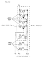
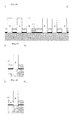
- FIG. 1 shows a conventional two-stage CMOS inverter using SGTs in which an output from a first inverter is input to a second inverter (Non-patent Literature 1).
- the first inverter includes two pMOS SGTs 01 and 02 and one nMOS SGT 03.
- the second inverter includes two pMOS SGTs 04 and 05 and two nMOS SGTs 06 and 07.
- the conventional two-stage CMOS inverter with the SGTs utilizes the SGTs in which each of a first power supply wiring line V SS and a second power supply wiring line V CC is supplied via a diffusion layer of a silicon substrate through contacts.
- the power supply lines of the nMOS and the pMOS are arranged in one side of a lower portion of a gate region that is different from a region on the substrate where the nMOS and the pMOS are arranged.
- a resistance of the diffusion layer is extremely higher than that of a metal wiring line for power supply.
- a driving current for the nMOS SGT is decreased.
- a driving current for the pMOS SGT is decreased.
- the driving current for the transistor is decreased, a speed of charging/discharging a capacitance at an output terminal of the inverter is reduced.
- a delay time of the inverter is increased.
- a metal wiring line is provided to the diffusion layer through many contacts, the first power supply voltage V SS is applied to a source of the nMOS SGT, and the second power supply voltage V CC is applied to a source of the pMOS SGT.
- the conventional SGT CMOS inverter forms contacts in the diffusion layer of a drain to be connected with a metal wiring line, thereby providing a first inverter output.
- the metal wiring line at the first inverter output is connected with a gate of polysilicon as a second inverter input through the contacts.
- a ratio of a contact area with respect to a circuit occupied area is large. Furthermore, when the resistances of the first power supply wiring line V SS and the second power supply wiring line V CC are increased, a delay time of the inverter is increased.
- CMOS inverter coupling circuit that uses SGTs and has at least two stages to reduce areas of a first power supply wiring line V SS and a second power supply wiring line V CC and also reduce resistances of the same.
- a semiconductor device comprising a CMOS inverter coupling circuit that couples n (n is two or above) CMOS inverters with each other, each of the n CMOS inverters having:
- the first MOS transistor in the n-1th CMOS inverter and the first MOS transistor in the nth CMOS inverter are arranged to be adjacent to each other
- the second MOS transistor in the nth CMOS inverter and the second MOS transistor in the n+1th CMOS inverter are arranged to be adjacent to each other
- the power supply wiring line for the first MOS transistor of the n-1th CMOS inverter is connected with the power supply wiring line for the first MOS transistor of the nth CMOS inverter on the source diffusion layers
- the power supply wiring line for the second MOS transistor of the nth CMOS inverter is connected with the power supply wiring line for the second MOS transistor of the n+1th CMOS inverter on the source diffusion layers.
- the n CMOS inverters arranged in a row with respect to the substrate are arranged in m rows (m is two or above) with respect to the substrate, the power supply wiring lines for the first MOS transistors of the respective CMOS inverters are connected with each other on the source diffusion layers, and the power supply wiring lines for the second MOS transistors of the respective CMOS inverters are connected with each other on the source diffusion layers.
- the first MOS transistor is a p-channel MOS transistor
- the second MOS transistor is an n-channel MOS transistor.
- the first MOS transistor is an n-channel MOS transistor
- the second MOS transistor is a p-channel MOS transistor.
- the first MOS transistor is an n-channel MOS transistor
- the second MOS transistor is a p-channel MOS transistor
- the number of the p-channel MOS transistors is double the number of the n-channel transistors.
- the first MOS transistor is a p-channel MOS transistor
- the second MOS transistor is an n-channel MOS transistor
- the number of the p-channel MOS transistors is double the number of the n-channel transistors.
- a semiconductor device comprising a CMOS inverter coupling circuit in which CMOS inverters on at least two stages are coupled with each other, the CMOS inverter having a first CMOS inverter and a second CMOS inverter, wherein the first CMOS inverter is a CMOS inverter having:
- a semiconductor device comprising a CMOS inverter coupling circuit in which CMOS inverters arranged in at least two rows and two columns are coupled with each other, wherein the CMOS inverter in a first row and a second column is a CMOS inverter having:
- the n-channel semiconductor device or the n-channel MOS transistor is used in the semiconductor device and has a structure in which a drain, a gate, and a source are arranged in a vertical direction with respect to a substrate and the gate surrounds an island-shaped semiconductor layer, insulating film layers are formed above and below the gate, a polysilicon wiring line surrounds a part of a drain diffusion layer in an island-shaped semiconductor lower layer, the drain diffusion layer, the polysilicon wiring line, the gate, and a source diffusion layer are salicided, and a metal wiring line is formed on the source diffusion layer.
- the p-channel semiconductor device or the p-channel MOS transistor is used in the semiconductor device and has a structure in which a drain, a gate, and a source are arranged in a vertical direction with respect to a substrate and the gate surrounds an island-shaped semiconductor layer, insulating film layers are formed above and below the gate, a polysilicon wiring line surrounds a part of a drain diffusion layer in an island-shaped semiconductor lower layer, a drain diffusion layer, the polysilicon wiring line, the gate, and a source diffusion layer are salicided, and a metal wiring line is formed on the source diffusion layer.
- the conventional two-stage CMOS inverter using the SGTs utilizes the SGTs having a structure where the first power supply voltage V SS and the second power supply voltage V CC are supplied to the diffusion layer of the silicon substrate through the contacts. That is, the power supply wiring lines of the nMOS SGTs and the pMOS SGTs are arranged in on one side of a lower portion of the gate region.
- the present invention has the first power supply wiring lines V SS and the second power supply wiring lines V CC supplied from the upper sides of both the nMOS SGTs and the pMOS SGTs and has:
- the present invention has the first power supply wiring lines V SS and the second power supply wiring lines V CC supplied from the upper sides of both the nMOS SGTs and the pMOS SGTs, and has:
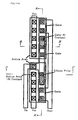
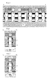
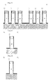
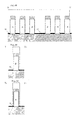
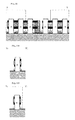
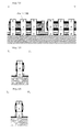
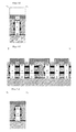
- FIGS. 2 , 3, 4, and 5 show a layout and cross-sectional structures of a semiconductor device according to the present invention.
- an output terminal wiring line 22 of an island-shaped semiconductor lower layer and a drain diffusion layer 23 are formed on a silicon oxide film 08, an island-shaped semiconductor layer 24 is formed thereon, a source diffusion layer 25 is formed on the island-shaped semiconductor layer 24, and a gate 26 is formed in a channel region of sidewalls sandwiched between the drain diffusion layer and the source diffusion layer through a gate insulating film, thereby forming an n-channel semiconductor device (an n-channel MOS transistor).
- island-shaped semiconductor lower portion wiring line 22 and drain diffusion layers 27 and 30 are formed on the silicon oxide film 08, island-shaped semiconductor layers 28 and 31 are formed thereon, source diffusion layers 29 and 32 are formed on the island-shaped semiconductor layers 28 and 31, the gate 26 is formed in a channel region of sidewalls sandwiched between each drain diffusion layer and each source diffusion layer through a gate insulating film, thereby forming p-channel semiconductor devices (p-channel MOS transistors).
- the two p-channel semiconductor devices and the one n-channel semiconductor device form a first inverter.
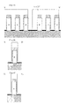
- an output terminal wiring line 09 of an island-shaped semiconductor lower layer and a drain diffusion layer 10 are formed on the silicon oxide film 08, an island-shaped semiconductor layer 11 is formed thereon, a source diffusion layer 12 is formed on the island-shaped semiconductor layer 11, and a gate 13 is formed in a channel region of sidewalls sandwiched between the drain diffusion layer and the source diffusion layer through a gate insulating film, thereby forming an n-channel semiconductor device.
- an island-shaped semiconductor lower portion wiring line 09 and drain diffusion layers 14 and 17 are formed on the silicon oxide film 08, island-shaped semiconductor layers 15 and 18 are formed thereon, source diffusion layers 16 and 19 are formed on the island-shaped semiconductor layers 15 and 18, and the gate 13 is formed in a channel region of sidewalls sandwiched between each drain diffusion layer and each source diffusion layer through a gate insulating film, thereby forming p-channel semiconductor devices.
- the two p-channel semiconductor devices and the one n-channel semiconductor device form a second inverter.
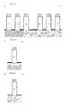
- a first power supply wiring line V SS 20 is formed on the source diffusion layers 12 and 25 of the n-channel semiconductor devices, and a second power supply wiring line V CC 33 is formed on the source diffusion layers 29 and 32 of the p-channel semiconductor devices in the first inverter.
- a second power supply wiring line V CC wiring line 21 is formed on the source diffusion layers 16 and 19 of the p-channel semiconductor devices in the second inverter.
- the gate 13 serves as an input terminal line of the second inverter.
- a contact 34 is formed to connect the gate 13 with the output terminal wiring line 22 of the lower layer in the first inverter. It is to be noted that the contact 34 is arranged between the silicon oxide film 08 and the first power supply wiring line V SS 20. That is, the contact 34 is arranged so as to vertically overlap at least a part of the first power supply wiring line V SS 20, thereby reducing an area required for wiring and achieving high integration (see FIG. 2 ).
- each of the first inverter and the second inverter is configured to have the two p-channel MOS transistors in the above-explained example, but each inverter may be configured to have the single p-channel MOS transistor. Additionally, in this case, it is possible to provide a circuit in which n (n is three or above) CMOS inverters each formed of the single p-channel MOS transistor are coupled with each other.
- n CMOS inverters when the n CMOS inverters are aligned with respect to a substrate, it is preferable to arrange the p-channel MOS transistor of an n-1th CMOS inverter and the p-channel MOS transistor of an nth CMOS inverter so as to be adjacent to each other and arrange the n-channel MOS transistor of the nth CMOS inverter and the n-channel MOS transistor of an n+1th CMOS inverter so as to be adjacent to each other.
- the two p-channel MOS transistors and the two n-channel transistors are arranged to be adjacent to each other, the first and second power supply wiring lines can be shortened, and resistances produced from the power supply wiring lines can be reduced.
- the p-channel MOS transistors and the n-channel MOS transistors may be counterchanged to constitute the plurality of inverters.
- the n CMOS inverters aligned with respect to the substrate may be arranged in m rows (m is two or above) with respect to the substrate.
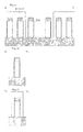
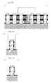
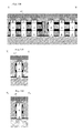
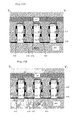
- FIG. 6 is an X-X' cross-sectional view of an SOI substrate in which silicon 100 is formed on a silicon oxide film, the silicon 100 is oxidized, and an oxide film 101 is formed.
- FIG. 7 is a Y 1 -Y' 1 cross-sectional view
- FIG. 8 is a Y 2 -Y' 2 cross-sectional view.
- the X-X' cross section corresponds to FIG. 3
- the Y 1 -Y' 1 cross section corresponds to FIG. 4
- the Y 2 -Y' 2 cross section corresponds to FIG. 5 .
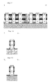
- Resists are used as masks, and the silicon 100 is etched based on reactive ion etching to form silicon pillars. Then, oxidation is carried out to form resists that are used to form p-type silicon ( FIG. 9 (X-X'), FIG. 10 (Y 1 -Y' 1 ), FIG. 11 (Y 2 -Y' 2 )).
- Boron is implanted based on, e.g., an ion implantation method to form p-type silicon 102 and 103 ( FIG. 12 (X-X'), FIG. 13 (Y 1 -Y' 1 ), FIG. 14 (Y 2 -Y' 2 )).
- the resist is separated to form resists that are used to form n-type silicon ( FIG. 15 (X-X'), FIG. 16 (Y 1 -Y' 1 ), FIG. 17 (Y 2 -Y' 2 )).
- Phosphor is implanted based on, e.g., the ion implantation method to form n-type silicon 104, 105, 106, and 107 ( FIG. 18 (X-X'), FIG. 19 (Y 1 -Y' 1 ), FIG. 20 (Y 2 -Y' 2 )).
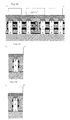
- the resists are delaminated, and a thermal process is carried out to ionize an impurity ( FIG. 21 (X-X'), FIG. 22 (Y 1 -Y' 1 ), FIG. 23 (Y 2 -Y' 2 )).
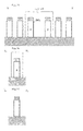
- a nitride film 108 is deposited, flattened based on CMP, and then etched back ( FIG. 24 (X-X'), FIG. 25 (Y 1 -Y' 1 ), FIG. 26 (Y 2 -Y' 2 )).
- Polysilicon 109 is deposited, flattened based on CMP, and then etched back ( FIG. 27 (X-X'), FIG. 28 (Y 1 -Y' 1 ), FIG. 29 (Y 2 -Y' 2 )).
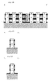
- a nitride film is deposited to remain in the form of a sidewall spacer on island-shaped semiconductor sidewalls 110, 111, 112, 113, 114, and 115 ( FIG. 30 (X-X'), FIG. 31 (Y 1 -Y' 1 ), FIG. 32 (Y 2 -Y' 2 )).
- the polysilicon is etched ( FIG. 33 (X-X'), FIG. 34 (Y 1 -Y' 1 ), FIG. 35 (Y 2 -Y' 2 )).
- FIG. 36 (X-X'), FIG. 37 (Y 1 -Y' 1 ), FIG. 38 (Y 2 -Y' 2 )).
- Polysilicon 116 is deposited, flattened based on CMP, and then etched back ( FIG. 39 (X-X'), FIG. 40 (Y 1 -Y' 1 ) FIG. 41 (Y 2 -Y' 2 )).
- the nitride film is etched ( FIG. 42 (X-X'), FIG. 43 (Y 1 -Y' 1 ), FIG. 44 (Y 2 -Y' 2 )).
- Resists that are used to form output terminal wiring lines of an island-shaped semiconductor lower layer is formed ( FIG. 45 (X-X'), FIG. 46 (Y 1 -Y' 1 ), FIG. 47 (Y 2 -Y' 2 )).
- the polysilicon is etched to form output terminal wiring lines 09 and 22 of the island-shaped semiconductor lower layer ( FIG. 48 (X-X'), FIG. 49 (Y 1 -Y' 1 ), FIG. 50 (Y 2 -Y' 2 )).
- the resists are delaminated ( FIG. 51 (X-X'), FIG. 52 (Y 1 -Y' 1 ), FIG. 53 (Y 2 -Y' 2 )).
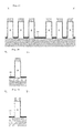
- An oxide film 117 is deposited, flattened based on CMP, and then etched back ( FIG. 54 (X-X'), FIG. 55 (Y 1 -Y' 1 ), FIG. 56 (Y 2 -Y' 2 )).
- a nitride film 118 is deposited, flattened based on CMP, and then etched back ( FIG. 57 (X-X'), FIG. 58 (Y 1 -Y' 1 ), FIG. 59 (Y 2 -Y' 2 )).
- Oxidation is carried out to form gate insulating films 119, 120, 121, 122, 123, and 124 ( FIG. 60 (X-X'), FIG. 61 (Y 1 -Y' 1 ), FIG. 62 (Y 2 -Y' 2 )).
- Polysilicon 125 is deposited, flattened based on CMP, and then etched back ( FIG. 63 (X-X'), FIG. 64 (Y 1 -Y' 1 ), FIG. 65 (Y 2 -Y' 2 )).
- a nitride film 126 is deposited, flattened based on CMP, and then etched back ( FIG. 66 (X-X'), FIG. 67 (Y 1 -Y' 1 ), FIG. 68 (Y 2 -Y' 2 )).
- Resists required to form input terminal lines, i.e., gates 13 and 26 are formed ( FIG. 69 (X-X'), FIG. 70 (Y 1 -Y' 1 ), FIG. 71 (Y 2 -Y' 2 )).
- the nitride film, the polysilicon, and the nitride film are etched to form the input terminal lines, i.e., the gates 13 and 26 ( FIG. 72 (X-X'), FIG. 73 (Y 1 -Y' 1 ), FIG. 74 (Y 2 -Y' 2 )).
- the resists are delaminated ( FIG. 75 (X-X'), FIG. 76 (Y 1 -Y' 1 ), FIG. 77 (Y 2 -Y' 2 )).
- An oxide film 127 is deposited, flattened based on CMP, and then etched back ( FIG. 78 (X-X'), FIG. 79 (Y 1 -Y' 1 ), FIG. 80 (Y 2 -Y' 2 )).
- Resists required to form a contact between the gates and the island-shaped semiconductor lower layer are formed ( FIG. 81 (X-X'), FIG. 82 (Y 1 -Y' 1 ), FIG. 83 (Y 2 -Y' 2 )).
- the oxide film is etched to form a contact 128 between the gates and the island-shaped semiconductor lower layer ( FIG. 84 (X-X'), FIG. 85 (Y 1 -Y' 1 ), FIG. 86 (Y 2 -Y' 2 )).
- the resists are delaminated ( FIG. 87 (X-X'), FIG. 88 (Y 1 -Y' 1 ), FIG. 89 (Y 2 -Y' 2 )).
- Polysilicon is deposited, flattened based on CMP, and then etched back, thereby forming a contact 34 between the gates and the island-shaped semiconductor lower layer ( FIG. 90 (X-X'), FIG. 91 (Y 1 -Y' 1 ), FIG. 92 (Y 2 -Y' 2 )).
- the oxide film is delaminated ( FIG. 93 (X-X'), FIG. 94 (Y 1 -Y' 1 ), FIG. 95 (Y 2 -Y' 2 )).
- FIG. 96 (X-X'), FIG. 97 (Y 1 -Y' 1 ), FIG. 98 (Y 2 -Y' 2 )).
- Resists required to form drain diffusion layers and source diffusion layers of n-channel semiconductor devices are formed ( FIG. 99 (X-X'), FIG. 100 (Y 1 -Y' 1 ), FIG. 101 (Y 2 -Y' 2 )).
- Arsenic is implanted based on, e.g., an ion implantation method to form drain diffusion layers 10 and 23 and source diffusion layers 12 and 25 ( FIG. 102 (X-X'), FIG. 103 (Y 1 -Y' 1 ), FIG. 104 (Y 2 -Y' 2 )).
- FIG. 105 A resist required to form drain diffusion layers and source diffusion layers of p-channel semiconductor devices is formed ( FIG. 105 (X-X'), FIG. 106 (Y 1 -Y' 1 ), FIG. 107 (Y 2 -Y' 2 )).
- Boron is implanted based on, e.g., the ion implantation method to form drain diffusion layers 14, 17, 27, and 30 and source diffusion layers 16, 19, 29, and 32 ( FIG. 108 (X-X'), FIG. 109 (Y 1 -Y' 1 ), FIG. 110 (Y 2 -Y' 2 )).
- the oxide film is delaminated, and a heat process is carried out to ionize an impurity ( FIG. 111 (X-X'), FIG. 112 (Y 1 -Y' 1 ), FIG. 113 (Y 2 -Y' 2 )).
- the oxide film is delaminated ( FIG. 114 (X-X'), FIG. 115 (Y 1 -Y' 1 ), FIG. 116 (Y 2 -Y' 2 )).
- a metal 129 e.g., cobalt or nickel is deposited based on sputtering or CVD ( FIG. 117 (X-X'), FIG. 118 (Y 1 -Y' 1 ), FIG. 119 (Y 2 -Y' 2 )).
- a heat process is carried out to react and salicide the metal and the silicon ( FIG. 120 (X-X'), FIG. 121 (Y 1 -Y' 1 ), FIG. 122 (Y 2 -Y' 2 )).
- the silicon and the unreacted metal are etched ( FIG. 123 (X-X'), FIG. 124 (Y 1 -Y' 1 ), FIG. 125 (Y 2 -Y' 2 )).
- An oxide film 130 is deposited, flattened based on CMP, and then etched back ( FIG. 126 (X-X'), FIG. 127 (Y 1 -Y' 1 ), FIG. 128 (Y 2 -Y' 2 )).
- Resists required to form contacts that connect the source diffusion layers 12 and 25 of the n-channel semiconductor devices with a first power supply wiring line V SS 20 and contacts that connect the source diffusion layers 29 and 32 of the p-channel semiconductor devices in a first inverter with a second power supply wiring line V CC 33 are formed, and resists required to form contacts that connect the source diffusion layers 16 and 19 of the p-channel semiconductor devices in a second inverter with a second power supply wiring line V CC 21 are formed ( FIG. 129 (X-X'), FIG. 130 (Y 1 -Y' 1 ), FIG. 131 (Y 2 -Y' 2 )).
- the oxide film is etched to form contacts 133 and 134 that connect the source diffusion layers 12 and 25 of the n-channel semiconductor devices with the first power supply wiring line V SS 20, contacts 135 and 136 that connect the source diffusion layers 29 and 32 of the p-channel semiconductor devices in the first inverter with the second power supply wiring line V CC 33, and contacts 132 and 131 that connect the source diffusion layers 16 and 19 of the p-channel semiconductor devices in the second inverter with the second power supply wiring line V CC 21 ( FIG. 132 (X-X'), FIG. 133 (Y 1 -Y' 1 ), FIG. 134 (Y 2 -Y' 2 )).
- the resists are delaminated ( FIG. 135 (X-X'), FIG. 136 (Y 1 -Y' 1 ), FIG. 137 (Y 2 -Y' 2 )).
- a metal 137 is deposited and flattened based on CMP ( FIG. 138 (X-X'), FIG. 139 (Y 1 -Y' 1 ), FIG. 140 (Y 2 -Y' 2 ).
- Resists required to form the first power supply wiring line V SS 20 and the second power supply wiring lines V CC 21 and 33 are formed ( FIG. 141 (X-X'), FIG. 142 (Y 1 -Y' 1 ), FIG. 143 (Y 2 -Y' 2 )).
- the metal is etched to form the first power supply wiring line V SS 20 and the second power supply wiring lines V CC 21 and 33 ( FIG. 144 (X-X'), FIG. 145 (Y 1 -Y' 1 ), FIG. 146 (Y 2 -Y' 2 )).
- the resists are delaminated ( FIG. 147 (X-X'), FIG. 148 (Y 1 -Y' 1 ), FIG. 149 (Y 2 -Y' 2 )).
- An oxide film 138 is deposited and flattened based on CMP ( FIG. 150 (X-X'), FIG. 151 (Y 1 -Y' 1 ), FIG. 152 (Y 2 -Y' 2 )).
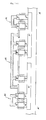
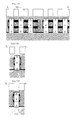
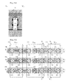
- FIG. 153 shows a CMOS inverter coupling circuit in which CMOS inverters are arranged in three rows and two columns as a specific example of the circuits arranged in m rows (m is two or above). It is to be noted that an example where one CMOS inverter has two P-channel MOS transistors (p-channel semiconductor devices) in a column direction will be explained, but the number of the P-channel MOS transistors in the column direction of the CMOS inverter may be one.
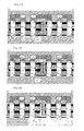
- FIG. 154 is an X 1 -X' 1 cross-sectional view
- FIG. 155 is an X 2 -X' 2 cross-sectional view
- FIG. 156 is an X 3 -X' 3 cross-sectional view
- FIG. 157 is a Y 1 -Y' 1 cross-sectional view
- FIG. 158 is a Y 2 -Y' 2 cross-sectional view.
- an output terminal wiring line 215 of an island-shaped semiconductor lower layer and a drain diffusion layer 216 are formed on a silicon oxide film 201, an island-shaped semiconductor layer 217 is formed thereon, a source diffusion layer 218 is formed on the island-shaped semiconductor layer 217, and a gate 219 is formed in a channel region of sidewalls sandwiched between the drain diffusion layer and the source diffusion layer through a gate insulating film, thereby forming an n-channel semiconductor device.
- the output terminal wiring line 215 of the island-shaped semiconductor lower layer and drain diffusion layers 220 and 223 are formed on the silicon oxide film 201, island-shaped semiconductor layers 221 and 224 are formed thereon, source diffusion layers 222 and 225 are formed on the island-shaped semiconductor layers 221 and 224, and the gate 219 is formed in the channel region of sidewalls sandwiched between the drain diffusion layers and the source diffusion layers through the gate insulating film, thereby forming p-channel semiconductor devices.
- the two p-channel semiconductor devices and the one n-channel semiconductor device form an inverter arranged in a third row and a second column.
- an output terminal wiring line 202 of the island-shaped semiconductor lower layer and a drain diffusion layer 203 are formed on the silicon oxide film 201, an island-shaped semiconductor layer 204 is formed thereon, a source diffusion layer 205 is formed on the island-shaped semiconductor layer 204, and a gate 206 is formed in a channel region of sidewalls sandwiched between the drain diffusion layer and the source diffusion layer through a gate insulating film, thereby forming an n-channel semiconductor device.
- an output terminal wiring line 202 of the island-shaped semiconductor lower layer and drain diffusion layers 207 and 210 are formed on the silicon oxide film 201, island-shaped semiconductor layers 208 and 211 are formed thereon, source diffusion layers 209 and 212 are formed on the island-shaped semiconductor layers 208 and 211, the gate 206 is formed in the channel region of sidewalls sandwiched between the drain diffusion layers and the source diffusion layers, thereby forming p-channel semiconductor devices.
- the two p-channel semiconductor devices and the one n-channel semiconductor device form an inverter arranged in a third row and a first column.
- the gate 206 serves as an input terminal line of the inverter arranged in the third row and the first column.
- a contact 227 is formed to connect the gate 206 with the output terminal wiring line 215 of the lower layer of the inverter arranged in the third row and the first column.
- an output terminal wiring line 315 of the island-shaped semiconductor lower layer and a drain diffusion layer 316 is formed on the silicon oxide film 201, an island-shaped semiconductor layer 317 is formed thereon, a source diffusion layer 318 is formed on the island-shaped semiconductor layer 317, and a gate 319 is formed in a channel region of sidewalls sandwiched between the drain diffusion layer and the source diffusion layer through a gate insulating film, thereby forming an n-channel semiconductor device.
- the output terminal wiring line 315 of the island-shaped semiconductor lower layer and drain diffusion layers 320 and 323 are formed on the silicon oxide film 201, island-shaped semiconductor layers 321 and 324 are formed thereon, source diffusion layers 322 and 325 are formed on the island-shaped semiconductor layers 321 and 324, and the gate 319 is formed in the channel region of sidewalls sandwiched between the drain diffusion layers and the source diffusion layers through the gate insulating film, thereby forming p-channel semiconductor device.
- the two p-channel semiconductor devices and the one n-channel semiconductor device form an inverter arranged in a second row and the second column.
- an output terminal wiring line 302 of the island-shaped semiconductor lower layer and a drain diffusion layer 303 are formed on the silicon oxide film 201, an island-shaped semiconductor layer 304 is formed thereon, a source diffusion layer 305 is formed on the island-shaped semiconductor layer 304, and a gate 306 is formed in a channel region of sidewalls sandwiched between the drain diffusion layer and the source diffusion layer through a gate insulating film, thereby forming an n-channel semiconductor device.
- the output terminal wiring line 302 of the island-shaped semiconductor lower layer and drain diffusion layers 307 and 310 are formed on the silicon oxide film 201, island-shaped semiconductor layers 308 and 311 are formed thereon, source diffusion layers 309 and 312 are formed on the island-shaped semiconductor layers 308 and 311, and the gate 306 is formed in the channel region of sidewalls sandwiched between the drain diffusion layers and the source diffusion layers through the gate insulating film, thereby forming p-channel semiconductor devices.
- the two p-channel semiconductor devices and the one n-channel semiconductor device form an inverter arranged in the second row and the first column.
- the gate 306 serves as an input terminal line of the inverter arranged in the second row and the first column.
- a contact 327 is formed to connect the gate 306 with the output terminal wiring line 315 of the lower layer of the inverter arranged in the second row and the second column.
- an output terminal wiring line 415 of the island-shaped semiconductor lower layer and a drain diffusion layer 416 are formed on the silicon oxide film 201, an island-shaped semiconductor layer 417 is formed thereon, a source diffusion layer 418 is formed on the island-shaped semiconductor layer 417, and a gate 419 is formed in a channel region of sidewalls sandwiched between the drain diffusion layer and the source diffusion layer through a gate insulating film, thereby forming an n-channel semiconductor device.
- the output terminal wiring line 415 of the island-shaped semiconductor lower layer and drain diffusion layers 420 and 423 are formed on the silicon oxide film 201, island-shaped semiconductor layers 421 and 424 are formed thereon, source diffusion layers 422 and 425 are formed on the island-shaped semiconductor layers 421 and 424, and the gate 419 is formed in the channel region of sidewalls sandwiched between the drain diffusion layers and the source diffusion layers through the gate insulating film, thereby forming p-channel semiconductor devices.
- the two p-channel semiconductor devices and the one n-channel semiconductor device form an inverter arranged in a first row and the second column.
- an output terminal wiring line 402 of the island-shaped semiconductor lower layer and a drain diffusion layer 403 are formed on the silicon oxide film 201, an island-shaped semiconductor layer 404 is formed thereon, a source diffusion layer 405 is formed on the island-shaped semiconductor layer 404, and a gate 406 is formed in a channel region of sidewalls sandwiched between the drain diffusion layer and the source diffusion layer through a gate insulating film, thereby forming an n-channel semiconductor device.
- the output terminal wiring line 402 of the island-shaped semiconductor lower layer and drain diffusion layers 407 and 410 are formed on the silicon oxide film 201, island-shaped semiconductor layers 408 and 411 are formed thereon, source diffusion layers 409 and 412 are formed on the island-shaped semiconductor layers 408 and 411, and the gate 406 is formed in the channel region of sidewalls sandwiched between the drain diffusion layers and the source diffusion layers through the gate insulating film, thereby forming p-channel semiconductor devices.
- the two p-channel semiconductor devices and the one n-channel semiconductor device form an inverter arranged in the first row and the first column.
- the gate 406 serves as an input terminal line of the inverter arranged in the first row and the first column.
- a contact 427 is formed to connect the gate 406 with the output terminal wiring line 415 of the lower layer of the inverter arranged in the first row and the second column.
- a first power supply wiring line V SS 213 is formed on the source diffusion layers 205, 218, 305, 318, 405, and 418 of the n-channel semiconductor devices
- a second power supply wiring line V CC 226 is formed on the source diffusion layers 222, 225, 322, 325, 422, and 425 of the p-channel semiconductor devices in the inverters arranged in the third row and the first column, in the second row and the first column, and in the first row and the first column.
- a second power supply wiring line V CC 214 is formed on the source diffusion layers 209, 212, 309, 312, 409, and 412 of the p-channel semiconductor devices in the inverters arranged in the third row and the first column, in the second row and the first column, and in the first row and the first column.
- the conventional two-stage CMOS inverter with the SGTs uses the SGTs in which the first power supply voltage V SS and the second power supply voltage V CC are supplied to the diffusion layers of the silicon substrate through the contacts. That is, the power supply wiring lines of the nMOS SGT and the pMOS SGT are arranged on one side of the lower portion of the gate region.
- the present invention has the first power supply wiring lines V SS and the second power supply wiring lines V CC supplied from upper sides of both the nMOS SGT and the pMOS SGT, and has:
- the present invention has the first power supply wiring lines V SS and the second power supply wiring lines V CC supplied from upper sides of both the nMOS SGT and the pMOS SGT, and has:
Abstract
Description
- The present invention relates to a semiconductor device.
- Integration of a semiconductor integrated circuit, especially an integrated circuit using MOS transistors is advancing. With this advancement of integration, miniaturization of the MOS transistor used in the circuit has proceeded to a nano level. Although a basic circuit of a digital circuit is an inverter circuit, when miniaturization of the MOS transistor constituting this inverter circuit advances, there occurs a problem that suppressing a leak current is difficult, reliability is reduced to a hot carrier effect, and an area share ratio of the circuit is hardly decreased because a necessary current amount must be assured. To solve such a problem, a surrounding gate transistor (SGT) having a structure in which a source, a gate, and a drain are arranged in a vertical direction with respect to a substrate and the gate surrounds an island-shaped semiconductor layer has been proposed, and a CMOS inverter circuit using the SGTs has been proposed (see, e.g.,
Patent Document 1,Patent Document 2, and Patent Document 3). -
FIG. 1 shows a conventional two-stage CMOS inverter using SGTs in which an output from a first inverter is input to a second inverter (Non-patent Literature 1). The first inverter includes two pMOS SGTs 01 and 02 and onenMOS SGT 03. The second inverter includes two pMOS SGTs 04 and 05 and two nMOS SGTs 06 and 07. The conventional two-stage CMOS inverter with the SGTs utilizes the SGTs in which each of a first power supply wiring line VSS and a second power supply wiring line VCC is supplied via a diffusion layer of a silicon substrate through contacts. That is, the power supply lines of the nMOS and the pMOS are arranged in one side of a lower portion of a gate region that is different from a region on the substrate where the nMOS and the pMOS are arranged. A resistance of the diffusion layer is extremely higher than that of a metal wiring line for power supply. When the resistances of the first power supply wiring line VSS and the second power supply wiring line VCC are increased, a source voltage applied to the nMOS SGT is increased beyond a first power supply voltage VSS and a source voltage applied to the pMOS SGT is reduced beyond a second power supply voltage VCC. When the source voltage for the nMOS SGT is increased beyond the first power supply voltage VSS, a driving current for the nMOS SGT is decreased. When the source voltage for the pMOS SGT is reduced beyond the second power supply voltage VCC, a driving current for the pMOS SGT is decreased. When the driving current for the transistor is decreased, a speed of charging/discharging a capacitance at an output terminal of the inverter is reduced. When the speed for charging/discharging the capacitance at the output terminal of the inverter is reduced, a delay time of the inverter is increased. Therefore, a metal wiring line is provided to the diffusion layer through many contacts, the first power supply voltage VSS is applied to a source of the nMOS SGT, and the second power supply voltage VCC is applied to a source of the pMOS SGT. - Further, the conventional SGT CMOS inverter forms contacts in the diffusion layer of a drain to be connected with a metal wiring line, thereby providing a first inverter output. The metal wiring line at the first inverter output is connected with a gate of polysilicon as a second inverter input through the contacts.
- That is, in the conventional substrate grounded type two-stage CMOS inverter using the SGTs, a ratio of a contact area with respect to a circuit occupied area is large. Furthermore, when the resistances of the first power supply wiring line VSS and the second power supply wiring line VCC are increased, a delay time of the inverter is increased.
-
- Patent Document 1: Japanese Patent Application Laid-open No.
71556-1990 - Patent Document 2: Japanese Patent Application Laid-open No.
188966-1990 - Patent Document 3: Japanese Patent Application Laid-open No.
145761-1991 - Non-patent Literature 1: S. Watanabe, K. Tsuchida, D. Takashima, Y. Oowaki, A. Nitayama, K. Hieda, H. Takato, K. Sunouchi, F. Horiguchi, K. Ohuchi, F. Masuoka, H. Hara, "A Nobel Circuit Technology with Surrounding Gate Transistors (SGT's) for Ultra High Density DRAM's", IEEE JSSC, Vol. 30, No. 9, 1995.
- Therefore, it is an object of the present invention to provide a semiconductor device including a highly integrated high-speed CMOS inverter coupling circuit that uses SGTs and has at least two stages to reduce areas of a first power supply wiring line VSS and a second power supply wiring line VCC and also reduce resistances of the same.
- According to one aspect of the present invention, there is provided a semiconductor device comprising a CMOS inverter coupling circuit that couples n (n is two or above) CMOS inverters with each other,
each of the n CMOS inverters having: - a first MOS transistor for a first conductivity type channel, which has a structure where a drain, a gate, and a source are arranged in a vertical direction with respect to a substrate and the gate surrounds an island-shaped semiconductor layer;
- a second MOS transistor for a second conductivity type channel different from the first conductivity type channel, which has a structure where a drain, a gate, and a source are arranged in a vertical direction with respect to the substrate and the gate surrounds an island-shaped semiconductor layer;
- an input terminal of the CMOS inverter arranged so as to connect the gate of the first MOS transistor with the gate of the second MOS transistor;
- an output terminal of the CMOS inverter arranged so as to connect a drain diffusion layer of the first MOS transistor with a drain diffusion layer of the second MOS transistor in an island-shaped semiconductor lower layer;
- a power supply wiring line for the first MOS transistor, which is arranged on a source diffusion layer of the first MOS transistor;
- a power supply wiring line for the second MOS transistor, which is arranged on a source diffusion layer of the second MOS transistor,
- According to a preferred aspect of the present invention, in the semiconductor device, when the n CMOS inverters are arranged in a row with respect to the substrate,
the first MOS transistor in the n-1th CMOS inverter and the first MOS transistor in the nth CMOS inverter are arranged to be adjacent to each other,
the second MOS transistor in the nth CMOS inverter and the second MOS transistor in the n+1th CMOS inverter are arranged to be adjacent to each other,
the power supply wiring line for the first MOS transistor of the n-1th CMOS inverter is connected with the power supply wiring line for the first MOS transistor of the nth CMOS inverter on the source diffusion layers, and
the power supply wiring line for the second MOS transistor of the nth CMOS inverter is connected with the power supply wiring line for the second MOS transistor of the n+1th CMOS inverter on the source diffusion layers. - According to another preferred aspect of the present invention, in the semiconductor device, the n CMOS inverters arranged in a row with respect to the substrate are arranged in m rows (m is two or above) with respect to the substrate,
the power supply wiring lines for the first MOS transistors of the respective CMOS inverters are connected with each other on the source diffusion layers, and
the power supply wiring lines for the second MOS transistors of the respective CMOS inverters are connected with each other on the source diffusion layers. - According to still another preferred aspect of the present invention, the first MOS transistor is a p-channel MOS transistor, and the second MOS transistor is an n-channel MOS transistor. Further, alternatively, the first MOS transistor is an n-channel MOS transistor, and the second MOS transistor is a p-channel MOS transistor.
- According to yet another preferred aspect of the present invention, the first MOS transistor is an n-channel MOS transistor, the second MOS transistor is a p-channel MOS transistor, and the number of the p-channel MOS transistors is double the number of the n-channel transistors. Furthermore, alternatively, the first MOS transistor is a p-channel MOS transistor, the second MOS transistor is an n-channel MOS transistor, and the number of the p-channel MOS transistors is double the number of the n-channel transistors.
- According to a further aspect of the present invention, there is provided a semiconductor device comprising a CMOS inverter coupling circuit in which CMOS inverters on at least two stages are coupled with each other, the CMOS inverter having a first CMOS inverter and a second CMOS inverter, wherein the first CMOS inverter is a CMOS inverter having:
- one n-channel semiconductor device having a structure where a drain, gate, and a source are arranged in a vertical direction with respect to a substrate and the gate surrounds an island-shaped semiconductor layer;
- two p-channel semiconductor devices each having a structure where a drain, a gate, and a source are arranged in the vertical direction with respect to the substrate and the gate surrounds an island-shaped semiconductor layer;
- an input terminal of the first CMOS inverter arranged so as to connect the gate of the n-channel semiconductor device with the gate of the p-channel semiconductor device;
- an output terminal of the first CMOS inverter arranged so as to connect a drain diffusion layer of the channel semiconductor device with a drain diffusion layer of the p-channel semiconductor device in an island-shaped semiconductor lower layer;
- a first power supply wiring line VSS connected with a source diffusion layer of the n-channel semiconductor device; and
- a second power supply wiring line VCC connected with source diffusion layers of the two p-channel semiconductor devices,
- the second CMOS inverter is a CMOS inverter having:
- one n-channel semiconductor device having a structure where a drain, a gate, and a source are arranged in the vertical direction with respect to the substrate and the gate surrounds an island-shaped semiconductor layer;
- two p-channel semiconductor devices each having a structure where a drain, a gate, and a source are arranged in the vertical direction with respect to the substrate and the gate surrounds an island-shaped semiconductor layer;
- an input terminal of the second CMOS inverter arranged so as to connect the gate of the n-channel semiconductor device with the gate of the p-channel semiconductor device;
- an output terminal of the second CMOS inverter arranged so as to connect a drain diffusion layer of the n-channel semiconductor device with a drain diffusion layer of the p-channel semiconductor device in the island-shaped semiconductor lower layer;
- a first power supply wiring line VSS connected with a source diffusion layer of the n-channel semiconductor device; and
- a second power supply wiring line VCC connected with source diffusion layers of the two p-channel semiconductor devices,
- the output terminal of the first CMOS inverter is connected with the input terminal of the second CMOS inverter,
- the first power supply wiring line VSS connected with the source diffusion layer of the n-channel semiconductor device in the first CMOS inverter is connected with the first power supply wiring line VSS connected with the source diffusion layer of the n-channel semiconductor device in the second CMOS inverter on the source diffusion layers, and
- the second power supply wiring line VCC connected with the source diffusion layers of the two p-channel semiconductor devices in the first CMOS inverter is connected with the second power supply wiring line VCC connected with the source diffusion layers of the two p-channel semiconductor devices in the second CMOS inverter on the source diffusion layers.
- Additionally, according to a still further aspect of the present invention, there is provided a semiconductor device comprising a CMOS inverter coupling circuit in which CMOS inverters arranged in at least two rows and two columns are coupled with each other, wherein the CMOS inverter in a first row and a second column is a CMOS inverter having:
- one n-channel semiconductor device having a structure where a drain, gate, and a source are arranged in a vertical direction with respect to a substrate and the gate surrounds an island-shaped semiconductor layer;
- two p-channel semiconductor devices each having a structure where a drain, a gate, and a source are arranged in the vertical direction with respect to the substrate and the gate surrounds an island-shaped semiconductor layer;
- an input terminal of the CMOS inverter in the first row and the second column, which is arranged so as to connect the gate of the n-channel semiconductor device with the gate of the p-channel semiconductor device;
- an output terminal of the CMOS inverter in the first row and the second column, which is arranged so as to connect a drain diffusion layer of the n-channel semiconductor device with a drain diffusion layer of the p-channel semiconductor device in an island-shaped semiconductor lower layer;
- a first power supply wiring line VSS connected with a source diffusion layer of the n-channel semiconductor device; and
- a second power supply wiring line VCC connected with source diffusion layers of the two p-channel semiconductor devices,
- the CMOS inverter in the first row and a first column is a CMOS inverter having:
- one n-channel semiconductor device having a structure where a drain, a gate, and a source are arranged in the vertical direction with respect to the substrate and the gate surrounds an island-shaped semiconductor layer;
- two p-channel semiconductor devices each having a structure where a drain, a gate, and a source are arranged in the vertical direction with respect to the substrate and the gate surrounds an island-shaped semiconductor layer;
- an input terminal of the CMOS inverter arranged in the first row and the first column, which is arranged so as to connect the gate of the n-channel semiconductor device with the gate of the p-channel semiconductor device;
- an output terminal of the CMOS inverter in the first row and the first column, which is arranged so as to connect a drain diffusion layer of the n-channel semiconductor device with a drain diffusion layer of the p-channel semiconductor device in the island-shaped semiconductor lower layer;
- a first power supply wiring line VSS connected with a source diffusion layer of the n-channel semiconductor device; and
- a second power supply wiring line VCC connected with source diffusion layers of the two p-channel semiconductor devices,
- the output terminal of the CMOS inverter in the first row and the second column is connected with the input terminal of the CMOS inverter in the first row and the first column in the CMOS inverter coupling circuit,
- the CMOS inverter in a second row and the second column is a CMOS inverter having:
- one n-channel semiconductor device having a structure where a drain, a gate, and a source are arranged in the vertical direction with respect to the substrate and the gate surrounds an island-shaped semiconductor layer;
- two p-channel semiconductor devices each having a structure where a drain, a gate, and a source are arranged in the vertical direction with respect to the substrate and the gate surrounds an island-shaped semiconductor layer;
- an input terminal of the CMOS inverter in the second row and the second column, which is arranged so as to connect the gate of the n-channel semiconductor device with the gate of the p-channel semiconductor device;
- an output terminal of the CMOS inverter in the second row and the second column arranged so as to connect a drain diffusion layer of the n-channel semiconductor device with a drain diffusion layer of the p-channel semiconductor device in the island-shaped semiconductor lower layer;
- a first power supply wiring line VSS connected with a source diffusion layer of the n-channel semiconductor device; and
- a second power supply wiring line VCC connected with source diffusion layers of the two p-channel semiconductor devices,
- the CMOS inverter in the second row and the first column is a CMOS inverter having:
- one n-channel semiconductor device having a structure where a drain, a gate, and a source are arranged in the vertical direction with respect to the substrate and the gate surrounds an island-shaped semiconductor layer;
- two p-channel semiconductor devices each having a structure where a drain, a gate, and a source are arranged in the vertical direction with respect to the substrate and the gate surrounds an island-shaped semiconductor layer;
- an input terminal of the CMOS inverter in the second row and the first column, which is arranged so as to connect the gate of the n-channel semiconductor device with the gate of the p-channel semiconductor device;
- an output terminal of the CMOS inverter in the second row and the first column, which is arranged so as to connect a drain diffusion layer of the n-channel semiconductor device with a drain diffusion layer of the p-channel semiconductor device in the island-shaped semiconductor lower layer;
- a first power supply wiring line VSS connected with a source diffusion layer of the n-channel semiconductor device; and
- a second power supply wiring line VCC connected with source diffusion layers of the two p-channel semiconductor devices,
- the output terminal of the CMOS inverter in the second row and the second column is connected with the input terminal of the CMOS inverter in the second row and the first column in the CMOS inverter coupling circuit, and
- the first power supply wiring line VSS connected with the source diffusion layer of the n-channel semiconductor device in the CMOS inverter in the first row and the second column;
- the first power supply wiring line VSS connected with the source diffusion layer of the n-channel semiconductor device in the CMOS inverter in the first row and the first column;
- the first power supply wiring line VSS connected with the source diffusion layer of the n-channel semiconductor device in the CMOS inverter in the second row and the second column; and
- the first power supply wiring line VSS connected with the source diffusion layer of the n-channel semiconductor device of the CMOS inverter in the second row and the first column are connected with each other on the source diffusion layers, and
- the second power supply wiring line VCC connected with the source diffusion layers of the two p-channel semiconductor devices in the CMOS inverter in the first row and the second column;
- the second power supply wiring line VCC connected with the source diffusion layers of the two p-channel semiconductor devices in the CMOS inverter in the second row and the second column;
- the second power supply wiring line VCC connected with the source diffusion layers of the two p-channel semiconductor devices in the CMOS inverter in the first row and the first column; and
- the second power supply wiring line VCC connected with the source diffusion layers of the two p-channel semiconductor devices in the CMOS inverter in the second row and the first column are connected with each other on the source diffusion layers.
- Further, according to a preferred aspect of the present invention, the n-channel semiconductor device or the n-channel MOS transistor is used in the semiconductor device and has a structure in which a drain, a gate, and a source are arranged in a vertical direction with respect to a substrate and the gate surrounds an island-shaped semiconductor layer,
insulating film layers are formed above and below the gate,
a polysilicon wiring line surrounds a part of a drain diffusion layer in an island-shaped semiconductor lower layer,
the drain diffusion layer, the polysilicon wiring line, the gate, and a source diffusion layer are salicided, and
a metal wiring line is formed on the source diffusion layer. - Furthermore, according to another preferred aspect of the present invention, the p-channel semiconductor device or the p-channel MOS transistor is used in the semiconductor device and has a structure in which a drain, a gate, and a source are arranged in a vertical direction with respect to a substrate and the gate surrounds an island-shaped semiconductor layer,
insulating film layers are formed above and below the gate,
a polysilicon wiring line surrounds a part of a drain diffusion layer in an island-shaped semiconductor lower layer,
a drain diffusion layer, the polysilicon wiring line, the gate, and a source diffusion layer are salicided, and
a metal wiring line is formed on the source diffusion layer. - The conventional two-stage CMOS inverter using the SGTs utilizes the SGTs having a structure where the first power supply voltage VSS and the second power supply voltage VCC are supplied to the diffusion layer of the silicon substrate through the contacts. That is, the power supply wiring lines of the nMOS SGTs and the pMOS SGTs are arranged in on one side of a lower portion of the gate region.
On the other hand, the present invention has the first power supply wiring lines VSS and the second power supply wiring lines VCC supplied from the upper sides of both the nMOS SGTs and the pMOS SGTs and has: - the first power supply wiring line VSS connected with the source diffusion layer of the n-channel semiconductor device of the first inverter;
- the first power supply wiring line VSS connected with the source diffusion layer of the n-channel semiconductor device of the second inverter;
- the second power supply wiring line VCC connected with the source diffusion layers of the two p-channel semiconductor devices of the first inverter; and
- the second power supply wiring line VCC connected with the source diffusion layers of the two p-channel semiconductor devices of the second inverter, thereby providing the semiconductor device formed of the highly integrated CMOS inverter coupling circuit with the SGTs that can reduce areas of the first power supply wiring lines VSS and the second power supply wiring lines VCC.
- Furthermore, the present invention has the first power supply wiring lines VSS and the second power supply wiring lines VCC supplied from the upper sides of both the nMOS SGTs and the pMOS SGTs, and has:
- the first power supply wiring line VSS connected with the source diffusion layer of the n-channel semiconductor device of the first inverter;
- the first power supply wiring line VSS connected with the source diffusion layer of the n-channel semiconductor device of the second inverter;
- the second power supply wiring line VCC connected with the source diffusion layers of the two p-channel semiconductor devices of the first inverter; and
- the second power supply wiring line VCC connected with the source diffusion layers of the two p-channel semiconductor devices of the second inverter, thereby providing the semiconductor device formed of the high-speed CMOS inverter coupling circuit with the SGTs that can reduce resistances of the first power supply wiring line VSS and the second power supply wiring line VCC.
- Since the output terminal wiring line that is arranged to connect the drain diffusion layer of the n-channel semiconductor device with the drain diffusion layer of the p-channel semiconductor device in the island-shaped semiconductor lower layer is provided:
- the contact that is used to connect the drain diffusion layer of the n-channel semiconductor device with the metal wiring line;
- the contact that is used to connect the drain diffusion layer of the p-channel semiconductor device with the metal wiring line; and
- the metal wiring line that connects the respective contacts with each other are no longer required, thereby providing the semiconductor device formed of the highly integrated CMOS inverter coupling circuit with the SGTs that can reduce resistances of the first power supply wiring line VSS and the second power supply wiring line Vcc.
-
-
FIG. 1(a) is a view showing a conventional two-stage CMOS inverter using SGTs; -
FIG. 1(b) is a view showing an equivalent circuit of the CMOS inverter depicted inFIG. 1(a) ; -
FIG. 1(c) is a view showing an A-A' cross-sectional view of the CMOS inverter depicted inFIG. 1(a) ; -
FIG. 1(d) is a view showing a B-B' cross-sectional view of the CMOS inverter depicted inFIG. 1(a) ; -
FIG. 1(e) is a view showing a C-C' cross-sectional view of the CMOS inverter depicted inFIG. 1(a) ; -
FIG. 2 is a layout of a semiconductor device according to the present invention; -
FIG. 3 is a cross-sectional view corresponding to an X-X' cross-sectional view inFIG. 1 of the semiconductor device according to the present invention; -
FIG. 4 is a cross-sectional view corresponding to a Y1-Y'1 cross-sectional view inFIG. 1 of the semiconductor device according to the present invention; -
FIG. 5 is a cross-sectional view corresponding to a Y2-Y'2 cross-sectional view inFIG. 1 of the semiconductor device according to the present invention; -
FIG. 6 is an X-X' cross-sectional process drawing showing a manufacture example of the semiconductor device according to the present invention; -
FIG. 7 is a Y1-Y'1 cross-sectional process drawing of the manufacture example of the semiconductor device according to the present invention; -
FIG. 8 is a Y2-Y'2 cross-sectional process drawing showing the manufacture example of the semiconductor device according to the present invention; -
FIG. 9 is an X-X' cross-sectional process drawing showing the manufacture example of the semiconductor device according to the present invention; -
FIG. 10 is a Y1-Y'1 cross-sectional process drawing showing the manufacture example of the semiconductor device according to the present invention; -
FIG. 11 is a Y2-Y'2 cross-sectional process drawing showing the manufacture example of the semiconductor device according to the present invention; -
FIG. 12 is an X-X' cross-sectional process drawing showing the manufacture example of the semiconductor device according to the present invention; -
FIG. 13 is a Y1-Y'1 cross-sectional process drawing showing the manufacture example of the semiconductor device according to the present invention; -
FIG. 14 is a Y2-Y'2 cross-sectional process drawing showing the manufacture example of the semiconductor device according to the present invention; -
FIG. 15 is an X-X' cross-sectional process drawing showing the manufacture example of the semiconductor device according to the present invention; -
FIG. 16 is a Y1-Y'1 cross-sectional process drawing showing the manufacture example of the semiconductor device according to the present invention; -
FIG. 17 is a Y2-Y'2 cross-sectional process drawing showing the manufacture example of the semiconductor device according to the present invention; -
FIG. 18 is an X-X' cross-sectional process drawing showing the manufacture example of the semiconductor device according to the present invention; -
FIG. 19 is a Y1-Y'1 cross-sectional process drawing showing the manufacture example of the semiconductor device according to the present invention; -
FIG. 20 is a Y2-Y'2 cross-sectional process drawing showing the manufacture example of the semiconductor device according to the present invention; -
FIG. 21 is an X-X' cross-sectional process drawing showing the manufacture example of the semiconductor device according to the present invention; -
FIG. 22 is a Y1-Y'1 cross-sectional process drawing showing the manufacture example of the semiconductor device according to the present invention; -
FIG. 23 is a Y2-Y'2 cross-sectional process drawing showing the manufacture example of the semiconductor device according to the present invention; -
FIG. 24 is an X-X' cross-sectional process drawing showing the manufacture example of the semiconductor device according to the present invention; -
FIG. 25 is a Y1-Y'1 cross-sectional process drawing showing the manufacture example of the semiconductor device according to the present invention; -
FIG. 26 is a Y2-Y'2 cross-sectional process drawing showing the manufacture example of the semiconductor device according to the present invention; -
FIG. 27 is an X-X' cross-sectional process drawing showing the manufacture example of the semiconductor device according to the present invention; -
FIG. 28 is a Y1-Y'1 cross-sectional process drawing showing the manufacture example of the semiconductor device according to the present invention; -
FIG. 29 is a Y2-Y'2 cross-sectional process drawing showing the manufacture example of the semiconductor device according to the present invention; -
FIG. 30 is an X-X' cross-sectional process drawing showing the manufacture example of the semiconductor device according to the present invention; -
FIG. 31 is a Y1-Y'1 cross-sectional process drawing showing the manufacture example of the semiconductor device according to the present invention; -
FIG. 32 is a Y2-Y'2 cross-sectional process drawing showing the manufacture example of the semiconductor device according to the present invention; -
FIG. 33 is an X-X' cross-sectional process drawing showing the manufacture example of the semiconductor device according to the present invention; -
FIG. 34 is a Y1-Y'1 cross-sectional process drawing showing the manufacture example of the semiconductor device according to the present invention; -
FIG. 35 is a Y2-Y'2 cross-sectional process drawing showing the manufacture example of the semiconductor device according to the present invention; -
FIG. 36 is an X-X' cross-sectional process drawing showing the manufacture example of the semiconductor device according to the present invention; -
FIG. 37 is a Y1-Y'1 cross-sectional process drawing showing the manufacture example of the semiconductor device according to the present invention; -
FIG. 38 is a Y2-Y'2 cross-sectional process drawing showing the manufacture example of the semiconductor device according to the present invention; -
FIG. 39 is an X-X' cross-sectional process drawing showing the manufacture example of the semiconductor device according to the present invention; -
FIG. 40 is a Y1-Y'1 cross-sectional process drawing showing the manufacture example of the semiconductor device according to the present invention; -
FIG. 41 is a Y2-Y'2 cross-sectional process drawing showing the manufacture example of the semiconductor device according to the present invention; -
FIG. 42 is an X-X' cross-sectional process drawing showing the manufacture example of the semiconductor device according to the present invention; -
FIG. 43 is a Y1-Y'1 cross-sectional process drawing showing the manufacture example of the semiconductor device according to the present invention; -
FIG. 44 is a Y2-Y'2 cross-sectional process drawing showing the manufacture example of the semiconductor device according to the present invention; -
FIG. 45 is an X-X' cross-sectional process drawing showing the manufacture example of the semiconductor device according to the present invention; -
FIG. 46 is a Y1-Y'1 cross-sectional process drawing showing the manufacture example of the semiconductor device according to the present invention; -
FIG. 47 is a Y2-Y'2 cross-sectional process drawing showing the manufacture example of the semiconductor device according to the present invention; -
FIG. 48 is an X-X' cross-sectional process drawing showing the manufacture example of the semiconductor device according to the present invention; -
FIG. 49 is a Y1-Y'1 cross-sectional process drawing showing the manufacture example of the semiconductor device according to the present invention; -
FIG. 50 is a Y2-Y'2 cross-sectional process drawing showing the manufacture example of the semiconductor device according to the present invention; -
FIG. 51 is an X-X' cross-sectional process drawing showing the manufacture example of the semiconductor device according to the present invention; -
FIG. 52 is a Y1-Y'1 cross-sectional process drawing showing the manufacture example of the semiconductor device according to the present invention; -
FIG. 53 is a Y2-Y'2 cross-sectional process drawing showing the manufacture example of the semiconductor device according to the present invention; -
FIG. 54 is an X-X' cross-sectional process drawing showing the manufacture example of the semiconductor device according to the present invention; -
FIG. 55 is a Y1-Y'1 cross-sectional process drawing showing the manufacture example of the semiconductor device according to the present invention; -
FIG. 56 is a Y2-Y'2 cross-sectional process drawing showing the manufacture example of the semiconductor device according to the present invention; -
FIG. 57 is an X-X' cross-sectional process drawing showing the manufacture example of the semiconductor device according to the present invention; -
FIG. 58 is a Y1-Y'1 cross-sectional process drawing showing the manufacture example of the semiconductor device according to the present invention; -
FIG. 59 is a Y2-Y'2 cross-sectional process drawing showing the manufacture example of the semiconductor device according to the present invention; -
FIG. 60 is an X-X' cross-sectional process drawing showing the manufacture example of the semiconductor device according to the present invention; -
FIG. 61 is a Y1-Y'1 cross-sectional process drawing showing the manufacture example of the semiconductor device according to the present invention; -
FIG. 62 is a Y2-Y'2 cross-sectional process drawing showing the manufacture example of the semiconductor device according to the present invention; -
FIG. 63 is an X-X' cross-sectional process drawing showing the manufacture example of the semiconductor device according to the present invention; -
FIG. 64 is a Y1-Y'1 cross-sectional process drawing showing the manufacture example of the semiconductor device according to the present invention; -
FIG. 65 is a Y2-Y'2 cross-sectional process drawing showing the manufacture example of the semiconductor device according to the present invention; -
FIG. 66 is an X-X' cross-sectional process drawing showing the manufacture example of the semiconductor device according to the present invention; -
FIG. 67 is a Y1-Y'1 cross-sectional process drawing showing the manufacture example of the semiconductor device according to the present invention; -
FIG. 68 is a Y2-Y'2 cross-sectional process drawing showing the manufacture example of the semiconductor device according to the present invention; -
FIG. 69 is an X-X' cross-sectional process drawing showing the manufacture example of the semiconductor device according to the present invention; -
FIG. 70 is a Y1-Y'1 cross-sectional process drawing showing the manufacture example of the semiconductor device according to the present invention; -
FIG. 71 is a Y2-Y'2 cross-sectional process drawing showing the manufacture example of the semiconductor device according to the present invention; -
FIG. 72 is an X-X' cross-sectional process drawing showing the manufacture example of the semiconductor device according to the present invention; -
FIG. 73 is a Y1-Y'1 cross-sectional process drawing showing the manufacture example of the semiconductor device according to the present invention; -
FIG. 74 is a Y2-Y'2 cross-sectional process drawing showing the manufacture example of the semiconductor device according to the present invention; -
FIG. 75 is an X-X' cross-sectional process drawing showing the manufacture example of the semiconductor device according to the present invention; -
FIG. 76 is a Y1-Y'1 cross-sectional process drawing showing the manufacture example of the semiconductor device according to the present invention; -
FIG. 77 is a Y2-Y'2 cross-sectional process drawing showing the manufacture example of the semiconductor device according to the present invention; -
FIG. 78 is an X-X' cross-sectional process drawing showing the manufacture example of the semiconductor device according to the present invention; -
FIG. 79 is a Y1-Y'1 cross-sectional process drawing showing the manufacture example of the semiconductor device according to the present invention; -
FIG. 80 is a Y2-Y'2 cross-sectional process drawing showing the manufacture example of the semiconductor device according to the present invention; -
FIG. 81 is an X-X' cross-sectional process drawing showing the manufacture example of the semiconductor device according to the present invention; -
FIG. 82 is a Y1-Y'1 cross-sectional process drawing showing the manufacture example of the semiconductor device according to the present invention; -
FIG. 83 is a Y2-Y'2 cross-sectional process drawing showing the manufacture example of the semiconductor device according to the present invention; -
FIG. 84 is an X-X' cross-sectional process drawing showing the manufacture example of the semiconductor device according to the present invention; -
FIG. 85 is a Y1-Y'1 cross-sectional process drawing showing the manufacture example of the semiconductor device according to the present invention; -
FIG. 86 is a Y2-Y'2 cross-sectional process drawing showing the manufacture example of the semiconductor device according to the present invention; -
FIG. 87 is an X-X' cross-sectional process drawing showing the manufacture example of the semiconductor device according to the present invention; -
FIG. 88 is a Y1-Y'1 cross-sectional process drawing showing the manufacture example of the semiconductor device according to the present invention; -
FIG. 89 is a Y2-Y'2 cross-sectional process drawing showing the manufacture example of the semiconductor device according to the present invention; -
FIG. 90 is an X-X' cross-sectional process drawing showing the manufacture example of the semiconductor device according to the present invention; -
FIG. 91 is a Y1-Y'1 cross-sectional process drawing showing the manufacture example of the semiconductor device according to the present invention; -
FIG. 92 is a Y2-Y'2 cross-sectional process drawing showing the manufacture example of the semiconductor device according to the present invention; -
FIG. 93 is an X-X' cross-sectional process drawing showing the manufacture example of the semiconductor device according to the present invention; -
FIG. 94 is a Y1-Y'1 cross-sectional process drawing showing the manufacture example of the semiconductor device according to the present invention; -
FIG. 95 is a Y2-Y'2 cross-sectional process drawing showing the manufacture example of the semiconductor device according to the present invention; -
FIG. 96 is an X-X' cross-sectional process drawing showing the manufacture example of the semiconductor device according to the present invention; -
FIG. 97 is a Y1-Y'1 cross-sectional process drawing showing the manufacture example of the semiconductor device according to the present invention; -
FIG. 98 is a Y2-Y'2 cross-sectional process drawing showing the manufacture example of the semiconductor device according to the present invention; -
FIG. 99 is an X-X' cross-sectional process drawing showing the manufacture example of the semiconductor device according to the present invention; -
FIG. 100 is a Y1-Y'1 cross-sectional process drawing showing the manufacture example of the semiconductor device according to the present invention; -
FIG. 101 is a Y2-Y'2 cross-sectional process drawing showing the manufacture example of the semiconductor device according to the present invention; -
FIG. 102 is an X-X' cross-sectional process drawing showing the manufacture example of the semiconductor device according to the present invention; -
FIG. 103 is a Y1-Y'1 cross-sectional process drawing showing the manufacture example of the semiconductor device according to the present invention; -
FIG. 104 is a Y2-Y'2 cross-sectional process drawing showing the manufacture example of the semiconductor device according to the present invention; -
FIG. 105 is an X-X' cross-sectional process drawing showing the manufacture example of the semiconductor device according to the present invention; -
FIG. 106 is a Y1-Y'1 cross-sectional process drawing showing the manufacture example of the semiconductor device according to the present invention; -
FIG. 107 is a Y2-Y'2 cross-sectional process drawing showing the manufacture example of the semiconductor device according to the present invention; -
FIG. 108 is an X-X' cross-sectional process drawing showing the manufacture example of the semiconductor device according to the present invention; -
FIG. 109 is a Y1-Y'1 cross-sectional process drawing showing the manufacture example of the semiconductor device according to the present invention; -
FIG. 110 is a Y2-Y'2 cross-sectional process drawing showing the manufacture example of the semiconductor device according to the present invention; -
FIG. 111 is an X-X' cross-sectional process drawing showing the manufacture example of the semiconductor device according to the present invention; -
FIG. 112 is a Y1-Y'1 cross-sectional process drawing showing the manufacture example of the semiconductor device according to the present invention; -
FIG. 113 is a Y2-Y'2 cross-sectional process drawing showing the manufacture example of the semiconductor device according to the present invention; -
FIG. 114 is an X-X' cross-sectional process drawing showing the manufacture example of the semiconductor device according to the present invention; -
FIG. 115 is a Y1-Y'1 cross-sectional process drawing showing the manufacture example of the semiconductor device according to the present invention; -
FIG. 116 is a Y2-Y'2 cross-sectional process drawing showing the manufacture example of the semiconductor device according to the present invention; -
FIG. 117 is an X-X' cross-sectional process drawing showing the manufacture example of the semiconductor device according to the present invention; -
FIG. 118 is a Y1-Y'1 cross-sectional process drawing showing the manufacture example of the semiconductor device according to the present invention; -
FIG. 119 is a Y2-Y'2 cross-sectional process drawing showing the manufacture example of the semiconductor device according to the present invention; -
FIG. 120 is an X-X' cross-sectional process drawing showing the manufacture example of the semiconductor device according to the present invention; -
FIG. 121 is a Y1-Y'1 cross-sectional process drawing showing the manufacture example of the semiconductor device according to the present invention; -
FIG. 122 is a Y2-Y'2 cross-sectional process drawing showing the manufacture example of the semiconductor device according to the present invention; -
FIG. 123 is an X-X' cross-sectional process drawing showing the manufacture example of the semiconductor device according to the present invention; -
FIG. 124 is a Y1-Y'1 cross-sectional process drawing showing the manufacture example of the semiconductor device according to the present invention; -
FIG. 125 is a Y2-Y'2 cross-sectional process drawing showing the manufacture example of the semiconductor device according to the present invention; -
FIG. 126 is an X-X' cross-sectional process drawing showing the manufacture example of the semiconductor device according to the present invention; -
FIG. 127 is a Y1-Y'1 cross-sectional process drawing showing the manufacture example of the semiconductor device according to the present invention; -
FIG. 128 is a Y2-Y'2 cross-sectional process drawing showing the manufacture example of the semiconductor device according to the present invention; -
FIG. 129 is an X-X' cross-sectional process drawing showing the manufacture example of the semiconductor device according to the present invention; -
FIG. 130 is a Y1-Y'1 cross-sectional process drawing showing the manufacture example of the semiconductor device according to the present invention; -
FIG. 131 is a Y2-Y'2 cross-sectional process drawing showing the manufacture example of the semiconductor device according to the present invention; -
FIG. 132 is an X-X' cross-sectional process drawing showing the manufacture example of the semiconductor device according to the present invention; -
FIG. 133 is a Y1-Y'1 cross-sectional process drawing showing the manufacture example of the semiconductor device according to the present invention; -
FIG. 134 is a Y2-Y'2 cross-sectional process drawing showing the manufacture example of the semiconductor device according to the present invention; -
FIG. 135 is an X-X' cross-sectional process drawing showing the manufacture example of the semiconductor device according to the present invention; -
FIG. 136 is a Y1-Y'1 cross-sectional process drawing showing the manufacture example of the semiconductor device according to the present invention; -
FIG. 137 is a Y2-Y'2 cross-sectional process drawing showing the manufacture example of the semiconductor device according to the present invention; -
FIG. 138 is an X-X' cross-sectional process drawing showing the manufacture example of the semiconductor device according to the present invention; -
FIG. 139 is a Y1-Y'1 cross-sectional process drawing showing the manufacture example of the semiconductor device according to the present invention; -
FIG. 140 is a Y2-Y'2 cross-sectional process drawing showing the manufacture example of the semiconductor device according to the present invention; -
FIG. 141 is an X-X' cross-sectional process drawing showing the manufacture example of the semiconductor device according to the present invention; -
FIG. 142 is a Y1-Y'1 cross-sectional process drawing showing the manufacture example of the semiconductor device according to the present invention; -
FIG. 143 is a Y2-Y'2 cross-sectional process drawing showing the manufacture example of the semiconductor device according to the present invention; -
FIG. 144 is an X-X' cross-sectional process drawing showing the manufacture example of the semiconductor device according to the present invention; -
FIG. 145 is a Y1-Y'1 cross-sectional process drawing showing the manufacture example of the semiconductor device according to the present invention; -
FIG. 146 is a Y2-Y'2 cross-sectional process drawing showing the manufacture example of the semiconductor device according to the present invention; -
FIG. 147 is an X-X' cross-sectional process drawing showing the manufacture example of the semiconductor device according to the present invention; -
FIG. 148 is a Y1-Y'1 cross-sectional process drawing showing the manufacture example of the semiconductor device according to the present invention; -
FIG. 149 is a Y2-Y'2 cross-sectional process drawing showing the manufacture example of the semiconductor device according to the present invention; -
FIG. 150 is an X-X' cross-sectional process drawing showing the manufacture example of the semiconductor device according to the present invention; -
FIG. 151 is a Y1-Y'1 cross-sectional process drawing showing the manufacture example of the semiconductor device according to the present invention; -
FIG. 152 is a Y2-Y'2 cross-sectional process drawing showing the manufacture example of the semiconductor device according to the present invention; -
FIG. 153 is a layout of the semiconductor device according to the present invention; -
FIG. 154 is a cross-sectional view corresponding to an X1-X'1 cross-sectional view inFIG. 153 of the semiconductor device according to the present invention; -
FIG. 155 is a cross-sectional view corresponding to an X2-X'2 cross-sectional view inFIG. 153 of the semiconductor device according to the present invention; -
FIG. 156 is a cross-sectional view corresponding to an X3-X'3 cross-sectional view inFIG. 153 of the semiconductor device according to the present invention; -
FIG. 157 is a cross-sectional view corresponding to a Y1-Y'1 cross-sectional view inFIG. 153 of the semiconductor device according to the present invention; and -
FIG. 158 is a cross-sectional view corresponding to a Y2-Y'2 cross-sectional view inFIG. 153 of the semiconductor device according to the present invention. -
- 01. nMOS SGT
- 02. pMOS SGT
- 03. nMOS SGT
- 04. pMOS SGT
- 05. pMOS SGT
- 06. nMOS SGT
- 07. nMOS SGT
- 08. silicon oxide film
- 09. output terminal wiring line of an island-shaped semiconductor lower layer
- 10. drain diffusion layer
- 11. island-shaped semiconductor layer
- 12. source diffusion layer
- 13. gate
- 14. drain diffusion layer
- 15. island-shaped semiconductor layer
- 16. source diffusion layer
- 17. drain diffusion layer
- 18. island-shaped semiconductor layer
- 19. source diffusion layer
- 20. first power supply wiring line VSS
- 21. second power supply wiring line VCC
- 22. output terminal wiring line of an island-shaped semiconductor lower layer
- 23. drain diffusion layer
- 24. island-shaped semiconductor layer
- 25. source diffusion layer
- 26. gate
- 27. drain diffusion layer
- 28. island-shaped semiconductor layer
- 29. source diffusion layer
- 30. drain diffusion layer
- 31. island-shaped semiconductor layer
- 32. source diffusion layer
- 33. second power supply wiring line Vcc
- 34. contact
- 100. silicon
- 101. oxide film
- 102. p-type silicon
- 103. p-type silicon
- 104. n-type silicon
- 105. n-type silicon
- 106. n-type silicon
- 107. n-type silicon
- 108. nitride film
- 109. polysilicon
- 110. nitride film sidewall spacer
- 111. nitride film sidewall spacer
- 112. nitride film sidewall spacer
- 113. nitride film sidewall spacer
- 114. nitride film sidewall spacer
- 115. nitride film sidewall spacer
- 116. polysilicon
- 117. oxide film
- 118. nitride film
- 119. gate oxide film
- 120. gate oxide film
- 121. gate oxide film
- 122. gate oxide film
- 123. gate oxide film
- 124. gate oxide film
- 125. polysilicon
- 126. nitride film
- 127. oxide film
- 128. contact between a gate and an island-shaped semiconductor lower layer
- 129. metal
- 130. oxide film
- 131. contact
- 132. contact
- 133. contact
- 134. contact
- 135. contact
- 136. contact
- 137. metal
- 138. oxide film
- 201. silicon oxide film
- 202. output terminal wiring line of an island-shaped semiconductor lower layer
- 203. drain diffusion layer
- 204. island-shaped semiconductor layer
- 205. source diffusion layer
- 206. gate
- 207. drain diffusion layer
- 208. island-shaped semiconductor layer
- 209. source diffusion layer
- 210. drain diffusion layer
- 211. island-shaped semiconductor layer
- 212. source diffusion layer
- 213. first power supply wiring line VSS
- 214. second power supply wiring line VCC
- 215. output terminal wiring line of an island-shaped semiconductor lower layer
- 216. drain diffusion layer
- 217. island-shaped semiconductor layer
- 218. source diffusion layer
- 219. gate
- 220. drain diffusion layer
- 221. island-shaped semiconductor layer
- 222. source diffusion layer
- 223. drain diffusion layer
- 224. island-shaped semiconductor layer
- 225. source diffusion layer
- 226. second power supply wiring line VCC
- 227. contact
- 302. output terminal wiring line of an island-shaped semiconductor lower layer
- 303. drain diffusion layer
- 304. island-shaped semiconductor layer
- 305. source diffusion layer
- 306. gate
- 307. drain diffusion layer
- 308. island-shaped semiconductor layer
- 309. source diffusion layer
- 310. drain diffusion layer
- 311. island-shaped semiconductor layer
- 312. source diffusion layer
- 315. output terminal wiring line of an island-shaped semiconductor lower layer
- 316. drain diffusion layer
- 317. island-shaped semiconductor layer
- 318. source diffusion layer
- 319. gate
- 320. drain diffusion layer
- 321. island-shaped semiconductor layer
- 322. source diffusion layer
- 323. drain diffusion layer
- 324. island-shaped semiconductor layer
- 325. source diffusion layer
- 327. contact
- 402. output terminal wiring line of an island-shaped semiconductor lower layer
- 403. drain diffusion layer
- 404. island-shaped semiconductor layer
- 405. source diffusion layer
- 406. gate
- 407. drain diffusion layer
- 408. island-shaped semiconductor layer
- 409. source diffusion layer
- 410. drain diffusion layer
- 411. island-shaped semiconductor layer
- 412. source diffusion layer
- 415. output terminal wiring line of an island-shaped semiconductor lower layer
- 416. drain diffusion layer
- 417. island-shaped semiconductor layer
- 418. source diffusion layer
- 419. gate
- 420. drain diffusion layer
- 421. island-shaped semiconductor layer
- 422. source diffusion layer
- 423. drain diffusion layer
- 424. island-shaped semiconductor layer
- 425. source diffusion layer
- 427. contact
- The present invention will now be explained based on an embodiment shown in the drawings. It is to be noted that the present invention is not restricted thereto. In particular, it is assumed that, as an MOS transistor, one formed of a silicon gate is included.
-
FIGS. 2 ,3, 4, and 5 show a layout and cross-sectional structures of a semiconductor device according to the present invention. In this embodiment, an outputterminal wiring line 22 of an island-shaped semiconductor lower layer and adrain diffusion layer 23 are formed on asilicon oxide film 08, an island-shapedsemiconductor layer 24 is formed thereon, asource diffusion layer 25 is formed on the island-shapedsemiconductor layer 24, and agate 26 is formed in a channel region of sidewalls sandwiched between the drain diffusion layer and the source diffusion layer through a gate insulating film, thereby forming an n-channel semiconductor device (an n-channel MOS transistor). Further, the island-shaped semiconductor lowerportion wiring line 22 and drain diffusion layers 27 and 30 are formed on thesilicon oxide film 08, island-shaped semiconductor layers 28 and 31 are formed thereon, source diffusion layers 29 and 32 are formed on the island-shaped semiconductor layers 28 and 31, thegate 26 is formed in a channel region of sidewalls sandwiched between each drain diffusion layer and each source diffusion layer through a gate insulating film, thereby forming p-channel semiconductor devices (p-channel MOS transistors). The two p-channel semiconductor devices and the one n-channel semiconductor device form a first inverter. - Furthermore, an output
terminal wiring line 09 of an island-shaped semiconductor lower layer and adrain diffusion layer 10 are formed on thesilicon oxide film 08, an island-shapedsemiconductor layer 11 is formed thereon, asource diffusion layer 12 is formed on the island-shapedsemiconductor layer 11, and agate 13 is formed in a channel region of sidewalls sandwiched between the drain diffusion layer and the source diffusion layer through a gate insulating film, thereby forming an n-channel semiconductor device. Moreover, an island-shaped semiconductor lowerportion wiring line 09 and drain diffusion layers 14 and 17 are formed on thesilicon oxide film 08, island-shaped semiconductor layers 15 and 18 are formed thereon, source diffusion layers 16 and 19 are formed on the island-shaped semiconductor layers 15 and 18, and thegate 13 is formed in a channel region of sidewalls sandwiched between each drain diffusion layer and each source diffusion layer through a gate insulating film, thereby forming p-channel semiconductor devices. The two p-channel semiconductor devices and the one n-channel semiconductor device form a second inverter. - A first power supply
wiring line V SS 20 is formed on the source diffusion layers 12 and 25 of the n-channel semiconductor devices, and a second power supplywiring line V CC 33 is formed on the source diffusion layers 29 and 32 of the p-channel semiconductor devices in the first inverter. A second power supply wiring line VCC wiring line 21 is formed on the source diffusion layers 16 and 19 of the p-channel semiconductor devices in the second inverter.
Thegate 13 serves as an input terminal line of the second inverter. Acontact 34 is formed to connect thegate 13 with the outputterminal wiring line 22 of the lower layer in the first inverter. It is to be noted that thecontact 34 is arranged between thesilicon oxide film 08 and the first power supplywiring line V SS 20. That is, thecontact 34 is arranged so as to vertically overlap at least a part of the first power supplywiring line V SS 20, thereby reducing an area required for wiring and achieving high integration (seeFIG. 2 ). - It is to be noted that each of the first inverter and the second inverter is configured to have the two p-channel MOS transistors in the above-explained example, but each inverter may be configured to have the single p-channel MOS transistor. Additionally, in this case, it is possible to provide a circuit in which n (n is three or above) CMOS inverters each formed of the single p-channel MOS transistor are coupled with each other. Specifically, when the n CMOS inverters are aligned with respect to a substrate, it is preferable to arrange the p-channel MOS transistor of an n-1th CMOS inverter and the p-channel MOS transistor of an nth CMOS inverter so as to be adjacent to each other and arrange the n-channel MOS transistor of the nth CMOS inverter and the n-channel MOS transistor of an n+1th CMOS inverter so as to be adjacent to each other. With such an arrangement, an entire structure of the circuit, the two p-channel MOS transistors and the two n-channel transistors are arranged to be adjacent to each other, the first and second power supply wiring lines can be shortened, and resistances produced from the power supply wiring lines can be reduced.
- Further, in the arrangement of the two CMOS inverters shown in
FIGS. 2 to 5 and the arrangement of the n CMOS inverters, the p-channel MOS transistors and the n-channel MOS transistors may be counterchanged to constitute the plurality of inverters. - Furthermore, in the above explanation, the n CMOS inverters aligned with respect to the substrate may be arranged in m rows (m is two or above) with respect to the substrate. In this case, it is preferable to mutually connect the power supply wiring lines for the p-channel MOS transistors in each CMOS inverter on the source diffusion layers and mutually connect the power supply wiring lines for the n-channel MOS transistors in each CMOS inverter on the source diffusion layers. With such an arrangement, as the entire structure of the circuit, the p-channel MOS transistors and the n-channel MOS transistors are arranged to be adjacent to each other in a row direction, the first and second power supply wiring lines can be shortened, and resistances produced from the power supply wiring lines can be reduced.
- An example of a manufacturing process for forming a structure of the semiconductor device according to the present invention will now be explained with reference to
FIGS. 6 to 152 .FIG. 6 is an X-X' cross-sectional view of an SOI substrate in whichsilicon 100 is formed on a silicon oxide film, thesilicon 100 is oxidized, and anoxide film 101 is formed. Furthermore,FIG. 7 is a Y1-Y'1 cross-sectional view, andFIG. 8 is a Y2-Y'2 cross-sectional view. The X-X' cross section corresponds toFIG. 3 , the Y1-Y'1 cross section corresponds toFIG. 4 , and the Y2-Y'2 cross section corresponds toFIG. 5 . - Resists are used as masks, and the
silicon 100 is etched based on reactive ion etching to form silicon pillars. Then, oxidation is carried out to form resists that are used to form p-type silicon (FIG. 9 (X-X'),FIG. 10 (Y1-Y'1),FIG. 11 (Y2-Y'2)). - Boron is implanted based on, e.g., an ion implantation method to form p-
type silicon 102 and 103 (FIG. 12 (X-X'),FIG. 13 (Y1-Y'1),FIG. 14 (Y2-Y'2)). - The resist is separated to form resists that are used to form n-type silicon (
FIG. 15 (X-X'),FIG. 16 (Y1-Y'1),FIG. 17 (Y2-Y'2)). - Phosphor is implanted based on, e.g., the ion implantation method to form n-
type silicon FIG. 18 (X-X'),FIG. 19 (Y1-Y'1),FIG. 20 (Y2-Y'2)). - The resists are delaminated, and a thermal process is carried out to ionize an impurity (
FIG. 21 (X-X'),FIG. 22 (Y1-Y'1),FIG. 23 (Y2-Y'2)). - A
nitride film 108 is deposited, flattened based on CMP, and then etched back (FIG. 24 (X-X'),FIG. 25 (Y1-Y'1),FIG. 26 (Y2-Y'2)). -
Polysilicon 109 is deposited, flattened based on CMP, and then etched back (FIG. 27 (X-X'),FIG. 28 (Y1-Y'1),FIG. 29 (Y2-Y'2)). - A nitride film is deposited to remain in the form of a sidewall spacer on island-shaped
semiconductor sidewalls FIG. 30 (X-X'),FIG. 31 (Y1-Y'1),FIG. 32 (Y2-Y'2)). - The polysilicon is etched (
FIG. 33 (X-X'),FIG. 34 (Y1-Y'1),FIG. 35 (Y2-Y'2)). - An oxide film is etched (
FIG. 36 (X-X'),FIG. 37 (Y1-Y'1),FIG. 38 (Y2-Y'2)). -
Polysilicon 116 is deposited, flattened based on CMP, and then etched back (FIG. 39 (X-X'),FIG. 40 (Y1-Y'1)FIG. 41 (Y2-Y'2)). - The nitride film is etched (
FIG. 42 (X-X'),FIG. 43 (Y1-Y'1),FIG. 44 (Y2-Y'2)). - Resists that are used to form output terminal wiring lines of an island-shaped semiconductor lower layer is formed (
FIG. 45 (X-X'),FIG. 46 (Y1-Y'1),FIG. 47 (Y2-Y'2)). - The polysilicon is etched to form output
terminal wiring lines FIG. 48 (X-X'),FIG. 49 (Y1-Y'1),FIG. 50 (Y2-Y'2)). - The resists are delaminated (
FIG. 51 (X-X'),FIG. 52 (Y1-Y'1),FIG. 53 (Y2-Y'2)). - An
oxide film 117 is deposited, flattened based on CMP, and then etched back (FIG. 54 (X-X'),FIG. 55 (Y1-Y'1),FIG. 56 (Y2-Y'2)). - A
nitride film 118 is deposited, flattened based on CMP, and then etched back (FIG. 57 (X-X'),FIG. 58 (Y1-Y'1),FIG. 59 (Y2-Y'2)). - Oxidation is carried out to form
gate insulating films FIG. 60 (X-X'),FIG. 61 (Y1-Y'1),FIG. 62 (Y2-Y'2)). -
Polysilicon 125 is deposited, flattened based on CMP, and then etched back (FIG. 63 (X-X'),FIG. 64 (Y1-Y'1),FIG. 65 (Y2-Y'2)). - A
nitride film 126 is deposited, flattened based on CMP, and then etched back (FIG. 66 (X-X'),FIG. 67 (Y1-Y'1),FIG. 68 (Y2-Y'2)). - Resists required to form input terminal lines, i.e.,
gates FIG. 69 (X-X'),FIG. 70 (Y1-Y'1),FIG. 71 (Y2-Y'2)). - The nitride film, the polysilicon, and the nitride film are etched to form the input terminal lines, i.e., the
gates 13 and 26 (FIG. 72 (X-X'),FIG. 73 (Y1-Y'1),FIG. 74 (Y2-Y'2)). - The resists are delaminated (
FIG. 75 (X-X'),FIG. 76 (Y1-Y'1),FIG. 77 (Y2-Y'2)). - An
oxide film 127 is deposited, flattened based on CMP, and then etched back (FIG. 78 (X-X'),FIG. 79 (Y1-Y'1),FIG. 80 (Y2-Y'2)). - Resists required to form a contact between the gates and the island-shaped semiconductor lower layer are formed (
FIG. 81 (X-X'),FIG. 82 (Y1-Y'1),FIG. 83 (Y2-Y'2)). - The oxide film is etched to form a
contact 128 between the gates and the island-shaped semiconductor lower layer (FIG. 84 (X-X'),FIG. 85 (Y1-Y'1),FIG. 86 (Y2-Y'2)). - The resists are delaminated (
FIG. 87 (X-X'),FIG. 88 (Y1-Y'1),FIG. 89 (Y2-Y'2)). - Polysilicon is deposited, flattened based on CMP, and then etched back, thereby forming a
contact 34 between the gates and the island-shaped semiconductor lower layer (FIG. 90 (X-X'),FIG. 91 (Y1-Y'1),FIG. 92 (Y2-Y'2)). - The oxide film is delaminated (
FIG. 93 (X-X'),FIG. 94 (Y1-Y'1),FIG. 95 (Y2-Y'2)). - Oxidation is performed (
FIG. 96 (X-X'),FIG. 97 (Y1-Y'1),FIG. 98 (Y2-Y'2)). - Resists required to form drain diffusion layers and source diffusion layers of n-channel semiconductor devices are formed (
FIG. 99 (X-X'),FIG. 100 (Y1-Y'1),FIG. 101 (Y2-Y'2)). - Arsenic is implanted based on, e.g., an ion implantation method to form drain diffusion layers 10 and 23 and source diffusion layers 12 and 25 (
FIG. 102 (X-X'),FIG. 103 (Y1-Y'1),FIG. 104 (Y2-Y'2)). - A resist required to form drain diffusion layers and source diffusion layers of p-channel semiconductor devices is formed (
FIG. 105 (X-X'),FIG. 106 (Y1-Y'1),FIG. 107 (Y2-Y'2)). - Boron is implanted based on, e.g., the ion implantation method to form drain diffusion layers 14, 17, 27, and 30 and source diffusion layers 16, 19, 29, and 32 (
FIG. 108 (X-X'),FIG. 109 (Y1-Y'1),FIG. 110 (Y2-Y'2)). - The oxide film is delaminated, and a heat process is carried out to ionize an impurity (
FIG. 111 (X-X'),FIG. 112 (Y1-Y'1),FIG. 113 (Y2-Y'2)). - The oxide film is delaminated (
FIG. 114 (X-X'),FIG. 115 (Y1-Y'1),FIG. 116 (Y2-Y'2)). - A
metal 129, e.g., cobalt or nickel is deposited based on sputtering or CVD (FIG. 117 (X-X'),FIG. 118 (Y1-Y'1),FIG. 119 (Y2-Y'2)). - A heat process is carried out to react and salicide the metal and the silicon (
FIG. 120 (X-X'),FIG. 121 (Y1-Y'1),FIG. 122 (Y2-Y'2)). - The silicon and the unreacted metal are etched (
FIG. 123 (X-X'),FIG. 124 (Y1-Y'1),FIG. 125 (Y2-Y'2)). - An
oxide film 130 is deposited, flattened based on CMP, and then etched back (FIG. 126 (X-X'),FIG. 127 (Y1-Y'1),FIG. 128 (Y2-Y'2)). - Resists required to form contacts that connect the source diffusion layers 12 and 25 of the n-channel semiconductor devices with a first power supply
wiring line V SS 20 and contacts that connect the source diffusion layers 29 and 32 of the p-channel semiconductor devices in a first inverter with a second power supplywiring line V CC 33 are formed, and resists required to form contacts that connect the source diffusion layers 16 and 19 of the p-channel semiconductor devices in a second inverter with a second power supplywiring line V CC 21 are formed (FIG. 129 (X-X'),FIG. 130 (Y1-Y'1),FIG. 131 (Y2-Y'2)). - The oxide film is etched to form
contacts wiring line V SS 20,contacts wiring line V CC 33, andcontacts FIG. 132 (X-X'),FIG. 133 (Y1-Y'1),FIG. 134 (Y2-Y'2)). - The resists are delaminated (
FIG. 135 (X-X'),FIG. 136 (Y1-Y'1),FIG. 137 (Y2-Y'2)). - A
metal 137 is deposited and flattened based on CMP (FIG. 138 (X-X'),FIG. 139 (Y1-Y'1),FIG. 140 (Y2-Y'2). - Resists required to form the first power supply
wiring line V SS 20 and the second power supply wiring lines VCC 21 and 33 are formed (FIG. 141 (X-X'),FIG. 142 (Y1-Y'1),FIG. 143 (Y2-Y'2)). - The metal is etched to form the first power supply
wiring line V SS 20 and the second power supply wiring lines VCC 21 and 33 (FIG. 144 (X-X'),FIG. 145 (Y1-Y'1),FIG. 146 (Y2-Y'2)). - The resists are delaminated (
FIG. 147 (X-X'),FIG. 148 (Y1-Y'1),FIG. 149 (Y2-Y'2)). - An
oxide film 138 is deposited and flattened based on CMP (FIG. 150 (X-X'),FIG. 151 (Y1-Y'1),FIG. 152 (Y2-Y'2)). - Further, although the CMOS inverter coupling circuit in which the CMOS inverters are arranged in one row and two columns has been explained in the example, the CMOS inverters may be arranged in two or more rows and two or more columns as shown in
FIG. 153. FIG. 153 shows a CMOS inverter coupling circuit in which CMOS inverters are arranged in three rows and two columns as a specific example of the circuits arranged in m rows (m is two or above). It is to be noted that an example where one CMOS inverter has two P-channel MOS transistors (p-channel semiconductor devices) in a column direction will be explained, but the number of the P-channel MOS transistors in the column direction of the CMOS inverter may be one. Furthermore, three or more CMOS inverter each having one P-channel MOS transistor may be arranged in the column direction. Moreover,FIG. 154 is an X1-X'1 cross-sectional view,FIG. 155 is an X2-X'2 cross-sectional view,FIG. 156 is an X3-X'3 cross-sectional view,FIG. 157 is a Y1-Y'1 cross-sectional view, andFIG. 158 is a Y2-Y'2 cross-sectional view. - In this example, an output
terminal wiring line 215 of an island-shaped semiconductor lower layer and adrain diffusion layer 216 are formed on asilicon oxide film 201, an island-shapedsemiconductor layer 217 is formed thereon, a source diffusion layer 218 is formed on the island-shapedsemiconductor layer 217, and agate 219 is formed in a channel region of sidewalls sandwiched between the drain diffusion layer and the source diffusion layer through a gate insulating film, thereby forming an n-channel semiconductor device. - Additionally, the output
terminal wiring line 215 of the island-shaped semiconductor lower layer and drain diffusion layers 220 and 223 are formed on thesilicon oxide film 201, island-shaped semiconductor layers 221 and 224 are formed thereon, source diffusion layers 222 and 225 are formed on the island-shaped semiconductor layers 221 and 224, and thegate 219 is formed in the channel region of sidewalls sandwiched between the drain diffusion layers and the source diffusion layers through the gate insulating film, thereby forming p-channel semiconductor devices. The two p-channel semiconductor devices and the one n-channel semiconductor device form an inverter arranged in a third row and a second column. - Further, an output
terminal wiring line 202 of the island-shaped semiconductor lower layer and a drain diffusion layer 203 are formed on thesilicon oxide film 201, an island-shaped semiconductor layer 204 is formed thereon, a source diffusion layer 205 is formed on the island-shaped semiconductor layer 204, and agate 206 is formed in a channel region of sidewalls sandwiched between the drain diffusion layer and the source diffusion layer through a gate insulating film, thereby forming an n-channel semiconductor device.
Furthermore, an outputterminal wiring line 202 of the island-shaped semiconductor lower layer and drain diffusion layers 207 and 210 are formed on thesilicon oxide film 201, island-shaped semiconductor layers 208 and 211 are formed thereon, source diffusion layers 209 and 212 are formed on the island-shaped semiconductor layers 208 and 211, thegate 206 is formed in the channel region of sidewalls sandwiched between the drain diffusion layers and the source diffusion layers, thereby forming p-channel semiconductor devices. The two p-channel semiconductor devices and the one n-channel semiconductor device form an inverter arranged in a third row and a first column. - The
gate 206 serves as an input terminal line of the inverter arranged in the third row and the first column. Acontact 227 is formed to connect thegate 206 with the outputterminal wiring line 215 of the lower layer of the inverter arranged in the third row and the first column. - Moreover, an output
terminal wiring line 315 of the island-shaped semiconductor lower layer and adrain diffusion layer 316 is formed on thesilicon oxide film 201, an island-shapedsemiconductor layer 317 is formed thereon, asource diffusion layer 318 is formed on the island-shapedsemiconductor layer 317, and agate 319 is formed in a channel region of sidewalls sandwiched between the drain diffusion layer and the source diffusion layer through a gate insulating film, thereby forming an n-channel semiconductor device. - Additionally, the output
terminal wiring line 315 of the island-shaped semiconductor lower layer and drain diffusion layers 320 and 323 are formed on thesilicon oxide film 201, island-shaped semiconductor layers 321 and 324 are formed thereon, source diffusion layers 322 and 325 are formed on the island-shaped semiconductor layers 321 and 324, and thegate 319 is formed in the channel region of sidewalls sandwiched between the drain diffusion layers and the source diffusion layers through the gate insulating film, thereby forming p-channel semiconductor device. The two p-channel semiconductor devices and the one n-channel semiconductor device form an inverter arranged in a second row and the second column. - Further, an output
terminal wiring line 302 of the island-shaped semiconductor lower layer and a drain diffusion layer 303 are formed on thesilicon oxide film 201, an island-shapedsemiconductor layer 304 is formed thereon, asource diffusion layer 305 is formed on the island-shapedsemiconductor layer 304, and agate 306 is formed in a channel region of sidewalls sandwiched between the drain diffusion layer and the source diffusion layer through a gate insulating film, thereby forming an n-channel semiconductor device. - Furthermore, the output
terminal wiring line 302 of the island-shaped semiconductor lower layer and drain diffusion layers 307 and 310 are formed on thesilicon oxide film 201, island-shaped semiconductor layers 308 and 311 are formed thereon, source diffusion layers 309 and 312 are formed on the island-shaped semiconductor layers 308 and 311, and thegate 306 is formed in the channel region of sidewalls sandwiched between the drain diffusion layers and the source diffusion layers through the gate insulating film, thereby forming p-channel semiconductor devices. The two p-channel semiconductor devices and the one n-channel semiconductor device form an inverter arranged in the second row and the first column. - The
gate 306 serves as an input terminal line of the inverter arranged in the second row and the first column. Acontact 327 is formed to connect thegate 306 with the outputterminal wiring line 315 of the lower layer of the inverter arranged in the second row and the second column. - Moreover, an output
terminal wiring line 415 of the island-shaped semiconductor lower layer and adrain diffusion layer 416 are formed on thesilicon oxide film 201, an island-shapedsemiconductor layer 417 is formed thereon, a source diffusion layer 418 is formed on the island-shapedsemiconductor layer 417, and agate 419 is formed in a channel region of sidewalls sandwiched between the drain diffusion layer and the source diffusion layer through a gate insulating film, thereby forming an n-channel semiconductor device. - Additionally, the output
terminal wiring line 415 of the island-shaped semiconductor lower layer and drain diffusion layers 420 and 423 are formed on thesilicon oxide film 201, island-shaped semiconductor layers 421 and 424 are formed thereon, source diffusion layers 422 and 425 are formed on the island-shaped semiconductor layers 421 and 424, and thegate 419 is formed in the channel region of sidewalls sandwiched between the drain diffusion layers and the source diffusion layers through the gate insulating film, thereby forming p-channel semiconductor devices. The two p-channel semiconductor devices and the one n-channel semiconductor device form an inverter arranged in a first row and the second column. - Further, an output
terminal wiring line 402 of the island-shaped semiconductor lower layer and a drain diffusion layer 403 are formed on thesilicon oxide film 201, an island-shapedsemiconductor layer 404 is formed thereon, a source diffusion layer 405 is formed on the island-shapedsemiconductor layer 404, and agate 406 is formed in a channel region of sidewalls sandwiched between the drain diffusion layer and the source diffusion layer through a gate insulating film, thereby forming an n-channel semiconductor device. - Furthermore, the output
terminal wiring line 402 of the island-shaped semiconductor lower layer and drain diffusion layers 407 and 410 are formed on thesilicon oxide film 201, island-shaped semiconductor layers 408 and 411 are formed thereon, source diffusion layers 409 and 412 are formed on the island-shaped semiconductor layers 408 and 411, and thegate 406 is formed in the channel region of sidewalls sandwiched between the drain diffusion layers and the source diffusion layers through the gate insulating film, thereby forming p-channel semiconductor devices. The two p-channel semiconductor devices and the one n-channel semiconductor device form an inverter arranged in the first row and the first column. - The
gate 406 serves as an input terminal line of the inverter arranged in the first row and the first column. Acontact 427 is formed to connect thegate 406 with the outputterminal wiring line 415 of the lower layer of the inverter arranged in the first row and the second column. - A first power supply
wiring line V SS 213 is formed on the source diffusion layers 205, 218, 305, 318, 405, and 418 of the n-channel semiconductor devices, and
a second power supplywiring line V CC 226 is formed on the source diffusion layers 222, 225, 322, 325, 422, and 425 of the p-channel semiconductor devices in the inverters arranged in the third row and the first column, in the second row and the first column, and in the first row and the first column.
A second power supplywiring line V CC 214 is formed on the source diffusion layers 209, 212, 309, 312, 409, and 412 of the p-channel semiconductor devices in the inverters arranged in the third row and the first column, in the second row and the first column, and in the first row and the first column. - As explained above, the conventional two-stage CMOS inverter with the SGTs uses the SGTs in which the first power supply voltage VSS and the second power supply voltage VCC are supplied to the diffusion layers of the silicon substrate through the contacts. That is, the power supply wiring lines of the nMOS SGT and the pMOS SGT are arranged on one side of the lower portion of the gate region.
On the other hand, the present invention has the first power supply wiring lines VSS and the second power supply wiring lines VCC supplied from upper sides of both the nMOS SGT and the pMOS SGT, and has: - the first power supply wiring line VSS connected with the source diffusion layer of the n-channel semiconductor device in the first inverter;
- the first power supply wiring line VSS connected with the source diffusion layer of the n-channel semiconductor device in the second inverter;
- the second power supply wiring line VCC connected with the source diffusion layers of the two p-channel semiconductor devices in the first inverter; and
- the second power supply wiring line VCC connected with the source diffusion layers of the two p-channel semiconductor devices in the second inverter, thereby providing a semiconductor device formed of the highly integrated CMOS inverter coupling circuit with SGTs in which areas of the first power supply wiring lines VSS and the second power supply wiring lines VCC are reduced.
- Moreover, since the present invention has the first power supply wiring lines VSS and the second power supply wiring lines VCC supplied from upper sides of both the nMOS SGT and the pMOS SGT, and has:
- the first power supply wiring line VSS connected with the source diffusion layer of the n-channel semiconductor device in the first inverter;
- the first power supply wiring line VSS connected with the source diffusion layer of the n-channel semiconductor device in the second inverter;
- the second power supply wiring line VCC connected with the source diffusion layers of the two p-channel semiconductor devices in the first inverter; and
- the second power supply wiring line VCC connected with the source diffusion layers of the two p-channel semiconductor devices in the second inverter,
- it is possible to provide a semiconductor device formed of the high-speed CMOS inverter coupling circuit with SGTs in which resistances of the first power supply wiring lines VSS and the second power supply wiring lines VCC are reduced.
- Since the output terminal wiring lines arranged to connect the drain diffusion layers of the n-channel semiconductor devices with the drain diffusion layers of the p-channel semiconductor devices in the island-shaped semiconductor lower layer are provided, it is possible to eliminate:
- a contact that is used to connect the drain diffusion layer of each n-channel semiconductor device with a metal wiring line;
- a contact that is used to connect the drain diffusion layer of each p-channel semiconductor device with the metal wiring line; and
- a metal wiring line connecting the respective contacts with each other is not required, thereby providing a semiconductor device formed of the highly integrated CMOS inverter coupling circuit using SGTs.
Claims (14)
- A semiconductor device comprising a CMOS inverter coupling circuit that couples n (n is two or above) CMOS inverters with each other,
each of the n CMOS inverters having:a first MOS transistor for a first conductivity type channel, which has a structure where a drain, a gate, and a source are arranged in a vertical direction with respect to a substrate and the gate surrounds an island-shaped semiconductor layer;a second MOS transistor for a second conductivity type channel different from the first conductivity type channel, which has a structure where a drain, a gate, and a source are arranged in a vertical direction with respect to the substrate and the gate surrounds an island-shaped semiconductor layer;an input terminal of the CMOS inverter arranged so as to connect the gate of the first MOS transistor with the gate of the second MOS transistor;an output terminal of the CMOS inverter arranged so as to connect a drain diffusion layer of the first MOS transistor with a drain diffusion layer of the second MOS transistor in an island-shaped semiconductor lower layer;a power supply wiring line for the first MOS transistor, which is arranged on a source diffusion layer of the first MOS transistor;a power supply wiring line for the second MOS transistor, which is arranged on a source diffusion layer of the second MOS transistor,wherein the semiconductor device further has a coupling portion that is used to connect the output terminal of an n-1th CMOS inverter with the input terminal of an nth CMOS inverter when arranging each of the n CMOS inverters with respect to the substrate, and the coupling portion is arranged between the substrate and the power supply wiring line for the first MOS transistor. - The semiconductor device according to claim 1, wherein, when the n CMOS inverters are arranged in a row with respect to the substrate,
the first MOS transistor of the n-1th CMOS inverter and the first MOS transistor of the nth CMOS inverter are arranged to be adjacent to each other,
the second MOS transistor of the nth CMOS inverter and the second MOS transistor of the n+1th CMOS inverter are arranged to be adjacent to each other,
the power supply wiring line for the first MOS transistor of the n-1th CMOS inverter is connected with the power supply wiring line for the first MOS transistor of the nth CMOS inverter on the source diffusion layers, and
the power supply wiring line for the second MOS transistor of the nth CMOS inverter is connected with the power supply wiring line for the second MOS transistor of the n+1th CMOS inverter on the source diffusion layers. - The semiconductor device according to claim 1 or 2, wherein the n CMOS inverters arranged in a row with respect to the substrate are arranged in m rows (m is two or above) with respect to the substrate,
the power supply wiring lines for the first MOS transistors of the respective CMOS inverters are connected with each other on the source diffusion layers, and
the power supply wiring lines for the second MOS transistors of the respective CMOS inverters are connected with each other on the source diffusion layers. - The semiconductor device according to any one of claims 1 to 3, wherein the first MOS transistor is a p-channel MOS transistor, and the second MOS transistor is an n-channel transistor.
- The semiconductor device according to any one of claims 1 to 3, wherein the first MOS transistor is an n-channel MOS transistor, and the second MOS transistor is an n-channel MOS transistor.
- The semiconductor device according to any one of claims 1 to 3, wherein the first MOS transistor is an n-channel MOS transistor, the second MOS transistor is a p-channel MOS transistor, and the number of the p-channel MOS transistors is double the number of the n-channel transistors.
- The semiconductor device according to any one of claims 1 to 3, wherein the first MOS transistor is a p-channel MOS transistor, the second MOS transistor is an n-channel MOS transistor, and the number of the p-channel MOS transistors is double the number of the n-channel transistors.
- An n-channel MOS transistor, which is used in the semiconductor device according to claims 4 to 7 and has a structure in which a drain, a gate, and a source are arranged in a vertical direction with respect to a substrate and the gate surrounds an island-shaped semiconductor layer,
wherein insulating film layers are formed above and below the gate,
a polysilicon wiring line surrounds a part of a drain diffusion layer in an island-shaped semiconductor lower layer,
the drain diffusion layer, the polysilicon wiring line, the gate, and a source diffusion layer are salicided, and
a metal wiring line is formed on the source diffusion layer. - A p-channel MOS transistor, which is used in the semiconductor device according to claims 4 to 7 and has a structure in which a drain, a gate, and a source are arranged in a vertical direction with respect to a substrate and the gate surrounds an island-shaped semiconductor layer,
wherein insulating film layers are formed above and below the gate,
a polysilicon wiring line surrounds a part of a drain diffusion layer in an island-shaped semiconductor lower layer,
a drain diffusion layer, the polysilicon wiring line, the gate, and a source diffusion layer are salicided, and
a metal wiring line is formed on the source diffusion layer. - A semiconductor device comprising a CMOS inverter coupling circuit in which CMOS inverters on at least two stages are coupled with each other, the CMOS inverter having a first CMOS inverter and a second CMOS inverter,
wherein the first CMOS inverter is a CMOS inverter having:an n-channel semiconductor device having a structure where a drain, gate, and a source are arranged in a vertical direction with respect to a substrate and the gate surrounds an island-shaped semiconductor layer;a p-channel semiconductor device having a structure where a drain, a gate, and a source are arranged in the vertical direction with respect to the substrate and the gate surrounds an island-shaped semiconductor layer;an input terminal of the first CMOS inverter arranged so as to connect the gate of the n-channel semiconductor device with the gate of the p-channel semiconductor device;an output terminal of the first CMOS inverter arranged so as to connect a drain diffusion layer of the n-channel semiconductor device with a drain diffusion layer of the p-channel semiconductor device in an island-shaped semiconductor lower layer;a first power supply wiring line connected with a source diffusion layer of the n-channel semiconductor device; anda second power supply wiring line connected with a source diffusion layer of the p-channel semiconductor device,the second CMOS inverter is a CMOS inverter having:an n-channel semiconductor device having a structure where a drain, a gate, and a source are arranged in the vertical direction with respect to the substrate and the gate surrounds an island-shaped semiconductor layer;a p-channel semiconductor device having a structure where a drain, a gate, and a source are arranged in the vertical direction with respect to the substrate and the gate surrounds an island-shaped semiconductor layer;an input terminal of the second CMOS inverter arranged so as to connect the gate of the n-channel semiconductor device with the gate of the p-channel semiconductor device;an output terminal of the second CMOS inverter arranged so as to connect a drain diffusion layer of the n-channel semiconductor device with a drain diffusion layer of the p-channel semiconductor device in the island-shaped semiconductor lower layer;a first power supply wiring line connected with a source diffusion layer of the n-channel semiconductor device; anda second power supply wiring line connected with a source diffusion layer of the p-channel semiconductor device,the output terminal of the first CMOS inverter connected with the input terminal of the second CMOS inverter,the first power supply wiring line connected with the source diffusion layer of the n-channel semiconductor device in the first CMOS inverter is connected with the first power supply wiring line VSS connected with the source diffusion layer of the n-channel semiconductor device in the second CMOS inverter on the source diffusion layers, andthe second power supply wiring line connected with the source diffusion layer of the p-channel semiconductor device in the first CMOS inverter is connected with the second power supply wiring line connected with the source diffusion layer of the p-channel semiconductor device in the second CMOS inverter on the source diffusion layers. - A semiconductor device comprising a CMOS inverter coupling circuit in which CMOS inverters on at least two stages are coupled with each other, the CMOS inverter having a first CMOS inverter and a second CMOS inverter,
wherein the first CMOS inverter is a CMOS inverter having:one n-channel semiconductor device having a structure where a drain, gate, and a source are arranged in a vertical direction with respect to a substrate and the gate surrounds an island-shaped semiconductor layer;two p-channel semiconductor devices each having a structure where a drain, a gate, and a source are arranged in the vertical direction with respect to the substrate and the gate surrounds an island-shaped semiconductor layer;an input terminal of the first CMOS inverter arranged so as to connect the gate of the n-channel semiconductor device with the gate of the p-channel semiconductor device;an output terminal of the first CMOS inverter arranged so as to connect a drain diffusion layer of the n-channel semiconductor device with a drain diffusion layer of the p-channel semiconductor device in an island-shaped semiconductor lower layer;a first power supply wiring line connected with a source diffusion layer of the n-channel semiconductor device; anda second power supply wiring line connected with source diffusion layers of the two p-channel semiconductor devices,the second CMOS inverter is a CMOS inverter having:one n-channel semiconductor device having a structure where a drain, a gate, and a source are arranged in the vertical direction with respect to the substrate and the gate surrounds an island-shaped semiconductor layer;two p-channel semiconductor devices each having a structure where a drain, a gate, and a source are arranged in the vertical direction with respect to the substrate and the gate surrounds an island-shaped semiconductor layer;an input terminal of the second CMOS inverter arranged so as to connect the gate of the n-channel semiconductor device with the gate of the p-channel semiconductor device;an output terminal of the second CMOS inverter arranged so as to connect a drain diffusion layer of the n-channel semiconductor device with a drain diffusion layer of the p-channel semiconductor device in the island-shaped semiconductor lower layer;a first power supply wiring line connected with a source diffusion layer of the n-channel semiconductor device; anda second power supply wiring line connected with source diffusion layers of the two p-channel semiconductor devices,the output terminal of the first CMOS inverter is connected with the input terminal of the second CMOS inverter,the first power supply wiring line VSS connected with the source diffusion layer of the n-channel semiconductor device in the first CMOS inverter is connected with the first power supply wiring line VSS connected with the source diffusion layer of the n-channel semiconductor device in the second CMOS inverter on the source diffusion layers, andthe second power supply wiring line VCC connected with the source diffusion layers of the p-channel semiconductor devices in the first CMOS inverter is connected with the second power supply wiring line VCC connected with the source diffusion layers of the two p-channel semiconductor devices in the second CMOS inverter on the source diffusion layers. - A semiconductor device comprising a CMOS inverter coupling circuit in which CMOS inverters arranged in at least two rows and two columns are coupled with each other,
wherein the CMOS inverter in a first row and a second column is a CMOS inverter having:one n-channel semiconductor device having a structure where a drain, gate, and a source are arranged in a vertical direction with respect to a substrate and the gate surrounds an island-shaped semiconductor layer;two p-channel semiconductor devices each having a structure where a drain, a gate, and a source are arranged in the vertical direction with respect to the substrate and the gate surrounds an island-shaped semiconductor layer;an input terminal of the CMOS inverter in the first row and the second column, which is arranged so as to connect the gate of the n-channel semiconductor device with the gate of the p-channel semiconductor device;an output terminal of the CMOS inverter in the first row and the second column, which is arranged so as to connect a drain diffusion layer of the n-channel semiconductor device with a drain diffusion layer of the p-channel semiconductor device in an island-shaped semiconductor lower layer;a first power supply wiring line connected with a source diffusion layer of the n-channel semiconductor device; anda second power supply wiring line connected with source diffusion layers of the two p-channel semiconductor devices,the CMOS inverter in the first row and a first column is a CMOS inverter having:one n-channel semiconductor device having a structure where a drain, a gate, and a source are arranged in the vertical direction with respect to the substrate and the gate surrounds an island-shaped semiconductor layer;two p-channel semiconductor devices each having a structure where a drain, a gate, and a source are arranged in the vertical direction with respect to the substrate and the gate surrounds an island-shaped semiconductor layer;an input terminal of the CMOS inverter in the first row and the first column, which is arranged so as to connect the gate of the n-channel semiconductor device with the gate of the p-channel semiconductor device;an output terminal of the CMOS inverter in the first row and the first column, which is arranged so as to connect a drain diffusion layer of the n-channel semiconductor device with a drain diffusion layer of the p-channel semiconductor device in the island-shaped semiconductor lower layer;a first power supply wiring line connected with a source diffusion layer of the n-channel semiconductor device; anda second power supply wiring line connected with source diffusion layers of the two p-channel semiconductor devices,the output terminal of the CMOS inverter in the first row and the second column is connected with the input terminal of the CMOS inverter in the first row and the first column in the CMOS inverter coupling circuit,the CMOS inverter in a second row and the second column is a CMOS inverter having:one n-channel semiconductor device having a structure where a drain, a gate, and a source are arranged in the vertical direction with respect to the substrate and the gate surrounds an island-shaped semiconductor layer;two p-channel semiconductor devices each having a structure where a drain, a gate, and a source are arranged in the vertical direction with respect to the substrate and the gate surrounds an island-shaped semiconductor layer;an input terminal of the CMOS inverter in the second row and the second column, which is arranged so as to connect the gate of the n-channel semiconductor device with the gate of the p-channel semiconductor device;an output terminal of the CMOS inverter in the second row and the second column arranged so as to connect a drain diffusion layer of the n-channel semiconductor device with a drain diffusion layer of the p-channel semiconductor device in the island-shaped semiconductor lower layer;a first power supply wiring line connected with a source diffusion layer of the n-channel semiconductor device; anda second power supply wiring line connected with source diffusion layers of the two p-channel semiconductor devices,the CMOS inverter in the second row and the first column is a CMOS inverter having:one n-channel semiconductor device having a structure where a drain, a gate, and a source are arranged in the vertical direction with respect to the substrate and the gate surrounds an island-shaped semiconductor layer;two p-channel semiconductor device having a structure where a drain, a gate, and a source are arranged in the vertical direction with respect to the substrate and the gate surrounds an island-shaped semiconductor layer;an input terminal of the CMOS inverter in the second row and the first column, which is arranged so as to connect the gate of the n-channel semiconductor device with the gate of the p-channel semiconductor device;an output terminal of the CMOS inverter in the second row and the first column, which is arranged so as to connect a drain diffusion layer of the n-channel semiconductor device with a drain diffusion layer of the p-channel semiconductor device in the island-shaped semiconductor lower layer;a first power supply wiring line connected with a source diffusion layer of the n-channel semiconductor device; anda second power supply wiring line connected with source diffusion layers of the two p-channel semiconductor devices,the output terminal of the CMOS inverter in the second row and the second column is connected with the input terminal of the CMOS inverter in the second row and the first column in the CMOS inverter coupling circuit, andthe first power supply wiring line connected with the source diffusion layer of the n-channel semiconductor device in the CMOS inverter in the first row and the second column;the first power supply wiring line connected with the source diffusion layer of the n-channel semiconductor device in the CMOS inverter in the first row and the first column;the first power supply wiring line connected with the source diffusion layer of the n-channel semiconductor device in the CMOS inverter in the second row and the second column; andthe first power supply wiring line VSS connected with the source diffusion layer of the n-channel semiconductor device of the CMOS inverter in the second row and the first column are connected with each other on the source diffusion layers, andthe second power supply wiring line connected with the source diffusion layers of the two p-channel semiconductor devices in the CMOS inverter in the first row and the second column;the second power supply wiring line connected with the source diffusion layers of the two p-channel semiconductor devices in the CMOS inverter in the second row and the second column;the second power supply wiring line connected with the source diffusion layers of the two p-channel semiconductor devices in the CMOS inverter in the first row and the first column; andthe second power supply wiring line connected with the source diffusion layers of the two p-channel semiconductor devices in the CMOS inverter in the second row and the first column are connected with each other on the source diffusion layers. - An n-channel semiconductor device, which is used in the semiconductor device according to any one of claims 10 to 12 and has a structure where a drain, gate, and a source are arranged in a vertical direction with respect to a substrate and the gate surrounds an island-shaped semiconductor layer,
wherein insulating film layers are formed above and below the gate,
a polysilicon wiring line surrounds a part of a drain diffusion layer in an island-shaped semiconductor lower layer,
the drain diffusion layer, the polysilicon wiring line, the gate, and a source diffusion layer are salicided, and
a metal wiring line is formed on the source diffusion layer. - A p-channel semiconductor device, which is used in the semiconductor device according to any one of claims 10 to 12 and has a structure where a drain, a gate, and a source are arranged in a vertical direction with respect to a substrate and the gate surrounds an island-shaped semiconductor layer,
wherein insulating film layers are formed above and below the gate,
a polysilicon wiring line surrounds a part of a drain diffusion layer in an island-shaped semiconductor lower layer,
the drain diffusion layer, the polysilicon wiring line, the gate, and a source diffusion layer are salicided, and
a metal wiring line is formed on the source diffusion layer.
Priority Applications (1)
| Application Number | Priority Date | Filing Date | Title |
|---|---|---|---|
| EP13174146.4A EP2645411A3 (en) | 2007-05-30 | 2008-02-14 | Semiconductor device |
Applications Claiming Priority (2)
| Application Number | Priority Date | Filing Date | Title |
|---|---|---|---|
| JP2007143891A JP5130596B2 (en) | 2007-05-30 | 2007-05-30 | Semiconductor device |
| PCT/JP2008/052450 WO2008146505A1 (en) | 2007-05-30 | 2008-02-14 | Semiconductor device |
Related Child Applications (1)
| Application Number | Title | Priority Date | Filing Date |
|---|---|---|---|
| EP13174146.4 Division-Into | 2013-06-27 |
Publications (3)
| Publication Number | Publication Date |
|---|---|
| EP2061075A1 true EP2061075A1 (en) | 2009-05-20 |
| EP2061075A4 EP2061075A4 (en) | 2012-06-13 |
| EP2061075B1 EP2061075B1 (en) | 2013-10-09 |
Family
ID=40074778
Family Applications (2)
| Application Number | Title | Priority Date | Filing Date |
|---|---|---|---|
| EP08711292.6A Active EP2061075B1 (en) | 2007-05-30 | 2008-02-14 | Semiconductor device |
| EP13174146.4A Withdrawn EP2645411A3 (en) | 2007-05-30 | 2008-02-14 | Semiconductor device |
Family Applications After (1)
| Application Number | Title | Priority Date | Filing Date |
|---|---|---|---|
| EP13174146.4A Withdrawn EP2645411A3 (en) | 2007-05-30 | 2008-02-14 | Semiconductor device |
Country Status (7)
| Country | Link |
|---|---|
| US (1) | US8039893B2 (en) |
| EP (2) | EP2061075B1 (en) |
| JP (1) | JP5130596B2 (en) |
| KR (1) | KR101057438B1 (en) |
| CN (1) | CN101542715B (en) |
| TW (1) | TW200847397A (en) |
| WO (1) | WO2008146505A1 (en) |
Cited By (3)
| Publication number | Priority date | Publication date | Assignee | Title |
|---|---|---|---|---|
| EP2284878A3 (en) * | 2009-08-11 | 2013-07-31 | Unisantis Electronics Singapore Pte. Ltd. | Semiconductor device and production method |
| US8642426B2 (en) | 2009-03-25 | 2014-02-04 | Unisantis Electronics Singapore Pte Ltd. | Semiconductor device and production method therefor |
| US8772881B2 (en) | 2009-06-05 | 2014-07-08 | Unisantis Electronics Singapore Pte Ltd. | Semiconductor device |
Families Citing this family (86)
| Publication number | Priority date | Publication date | Assignee | Title |
|---|---|---|---|---|
| JP5122212B2 (en) * | 2007-08-02 | 2013-01-16 | ユニサンティス エレクトロニクス シンガポール プライベート リミテッド | Semiconductor device |
| US8183628B2 (en) | 2007-10-29 | 2012-05-22 | Unisantis Electronics Singapore Pte Ltd. | Semiconductor structure and method of fabricating the semiconductor structure |
| US8598650B2 (en) | 2008-01-29 | 2013-12-03 | Unisantis Electronics Singapore Pte Ltd. | Semiconductor device and production method therefor |
| JP5317343B2 (en) | 2009-04-28 | 2013-10-16 | ユニサンティス エレクトロニクス シンガポール プライベート リミテッド | Semiconductor device and manufacturing method thereof |
| KR100946084B1 (en) * | 2008-03-27 | 2010-03-10 | 주식회사 하이닉스반도체 | Vertical transistor for semiconductor device and manufacturing method of the same |
| JP4487221B1 (en) * | 2009-04-17 | 2010-06-23 | 日本ユニサンティスエレクトロニクス株式会社 | Semiconductor device |
| JP5323610B2 (en) * | 2009-08-18 | 2013-10-23 | ユニサンティス エレクトロニクス シンガポール プライベート リミテッド | Semiconductor device and manufacturing method thereof |
| JP5006379B2 (en) | 2009-09-16 | 2012-08-22 | ユニサンティス エレクトロニクス シンガポール プライベート リミテッド | Semiconductor device |
| JP5356970B2 (en) * | 2009-10-01 | 2013-12-04 | ユニサンティス エレクトロニクス シンガポール プライベート リミテッド | Semiconductor device |
| JP5006375B2 (en) * | 2009-12-10 | 2012-08-22 | ユニサンティス エレクトロニクス シンガポール プライベート リミテッド | Semiconductor device and manufacturing method thereof |
| JP4912513B2 (en) | 2010-03-08 | 2012-04-11 | ユニサンティス エレクトロニクス シンガポール プライベート リミテッド | Solid-state imaging device |
| US8487357B2 (en) | 2010-03-12 | 2013-07-16 | Unisantis Electronics Singapore Pte Ltd. | Solid state imaging device having high sensitivity and high pixel density |
| JP5128630B2 (en) | 2010-04-21 | 2013-01-23 | ユニサンティス エレクトロニクス シンガポール プライベート リミテッド | Semiconductor device |
| JP5066590B2 (en) | 2010-06-09 | 2012-11-07 | ユニサンティス エレクトロニクス シンガポール プライベート リミテッド | Semiconductor device and manufacturing method thereof |
| JP5087655B2 (en) | 2010-06-15 | 2012-12-05 | ユニサンティス エレクトロニクス シンガポール プライベート リミテッド | Semiconductor device and manufacturing method thereof |
| KR101723864B1 (en) * | 2010-10-08 | 2017-04-07 | 삼성전자주식회사 | Semiconductor Device With Vertical Channel Transistor And Method Of Fabricating The Same |
| US8564034B2 (en) | 2011-09-08 | 2013-10-22 | Unisantis Electronics Singapore Pte. Ltd. | Solid-state imaging device |
| US8669601B2 (en) | 2011-09-15 | 2014-03-11 | Unisantis Electronics Singapore Pte. Ltd. | Method for producing semiconductor device and semiconductor device having pillar-shaped semiconductor |
| US8772175B2 (en) | 2011-12-19 | 2014-07-08 | Unisantis Electronics Singapore Pte. Ltd. | Method for manufacturing semiconductor device and semiconductor device |
| US8916478B2 (en) | 2011-12-19 | 2014-12-23 | Unisantis Electronics Singapore Pte. Ltd. | Method for manufacturing semiconductor device and semiconductor device |
| US8598633B2 (en) * | 2012-01-16 | 2013-12-03 | GlobalFoundries, Inc. | Semiconductor device having contact layer providing electrical connections |
| US8748938B2 (en) | 2012-02-20 | 2014-06-10 | Unisantis Electronics Singapore Pte. Ltd. | Solid-state imaging device |
| JP5686931B1 (en) | 2013-07-30 | 2015-03-18 | ユニサンティス エレクトロニクス シンガポール プライベート リミテッドUnisantis Electronics Singapore Pte Ltd. | Semiconductor device |
| WO2015015565A1 (en) | 2013-07-30 | 2015-02-05 | ユニサンティス エレクトロニクス シンガポール プライベート リミテッド | Semiconductor device |
| JP5677642B1 (en) | 2013-08-08 | 2015-02-25 | ユニサンティス エレクトロニクス シンガポール プライベート リミテッドUnisantis Electronics Singapore Pte Ltd. | Semiconductor device |
| WO2015019470A1 (en) | 2013-08-08 | 2015-02-12 | ユニサンティス エレクトロニクス シンガポール プライベート リミテッド | Semiconductor device |
| WO2015033381A1 (en) * | 2013-09-03 | 2015-03-12 | ユニサンティス エレクトロニクス シンガポール プライベート リミテッド | Semiconductor device |
| WO2015033382A1 (en) | 2013-09-03 | 2015-03-12 | ユニサンティス エレクトロニクス シンガポール プライベート リミテッド | Semiconductor device |
| CN103531635B (en) * | 2013-09-18 | 2016-03-16 | 北京大学 | A kind of vertical ring gate transistor based on nano wire and preparation method thereof |
| JP5688189B1 (en) * | 2013-10-23 | 2015-03-25 | ユニサンティス エレクトロニクス シンガポール プライベート リミテッドUnisantis Electronics Singapore Pte Ltd. | Semiconductor device |
| US9373623B2 (en) * | 2013-12-20 | 2016-06-21 | Taiwan Semiconductor Manufacturing Company Limited | Multi-layer semiconductor structures for fabricating inverter chains |
| JP5719944B1 (en) | 2014-01-20 | 2015-05-20 | ユニサンティス エレクトロニクス シンガポール プライベート リミテッドUnisantis Electronics Singapore Pte Ltd. | Semiconductor device |
| WO2015155862A1 (en) | 2014-04-10 | 2015-10-15 | ユニサンティス エレクトロニクス シンガポール プライベート リミテッド | Semiconductor device |
| JP5770406B1 (en) | 2014-04-10 | 2015-08-26 | ユニサンティス エレクトロニクス シンガポール プライベート リミテッドUnisantis Electronics Singapore Pte Ltd. | Semiconductor device |
| JP5838488B1 (en) * | 2014-04-22 | 2016-01-06 | ユニサンティス エレクトロニクス シンガポール プライベート リミテッドUnisantis Electronics Singapore Pte Ltd. | Semiconductor device |
| JP5804230B1 (en) * | 2014-04-22 | 2015-11-04 | ユニサンティス エレクトロニクス シンガポール プライベート リミテッドUnisantis Electronics Singapore Pte Ltd. | Semiconductor device |
| US9755033B2 (en) | 2014-06-13 | 2017-09-05 | Taiwan Semiconductor Manufacturing Co., Ltd. | Semiconductor device and method of forming vertical structure |
| WO2015199644A1 (en) | 2014-06-23 | 2015-12-30 | Intel Corporation | Techniques for forming vertical transistor architectures |
| US9490331B2 (en) * | 2014-06-30 | 2016-11-08 | Taiwan Semiconductor Manufacturing Company Limited | Formation of semiconductor arrangement comprising buffer layer and semiconductor column overlying buffer layer |
| JP5990843B2 (en) | 2014-07-14 | 2016-09-14 | ユニサンティス エレクトロニクス シンガポール プライベート リミテッドUnisantis Electronics Singapore Pte Ltd. | Semiconductor device manufacturing method and semiconductor device |
| WO2016021020A1 (en) | 2014-08-07 | 2016-02-11 | ユニサンティス エレクトロニクス シンガポール プライベート リミテッド | Semiconductor device manufacturing method and semiconductor device |
| US9673054B2 (en) * | 2014-08-18 | 2017-06-06 | Micron Technology, Inc. | Array of gated devices and methods of forming an array of gated devices |
| JP5989238B2 (en) | 2014-08-28 | 2016-09-07 | ユニサンティス エレクトロニクス シンガポール プライベート リミテッドUnisantis Electronics Singapore Pte Ltd. | Semiconductor device and method for manufacturing semiconductor device |
| WO2016035213A1 (en) | 2014-09-05 | 2016-03-10 | ユニサンティス エレクトロニクス シンガポール プライベート リミテッド | Semiconductor device |
| JP5841696B1 (en) * | 2014-11-27 | 2016-01-13 | ユニサンティス エレクトロニクス シンガポール プライベート リミテッドUnisantis Electronics Singapore Pte Ltd. | Columnar semiconductor device and manufacturing method thereof |
| KR101743864B1 (en) | 2015-01-28 | 2017-06-07 | 허천신 | Vertical type cmos inverter device |
| JP6122556B2 (en) | 2015-03-03 | 2017-04-26 | ユニサンティス エレクトロニクス シンガポール プライベート リミテッドUnisantis Electronics Singapore Pte Ltd. | Semiconductor device |
| US10121553B2 (en) | 2015-09-30 | 2018-11-06 | Sunrise Memory Corporation | Capacitive-coupled non-volatile thin-film transistor NOR strings in three-dimensional arrays |
| US11120884B2 (en) | 2015-09-30 | 2021-09-14 | Sunrise Memory Corporation | Implementing logic function and generating analog signals using NOR memory strings |
| US9842651B2 (en) | 2015-11-25 | 2017-12-12 | Sunrise Memory Corporation | Three-dimensional vertical NOR flash thin film transistor strings |
| US9892800B2 (en) | 2015-09-30 | 2018-02-13 | Sunrise Memory Corporation | Multi-gate NOR flash thin-film transistor strings arranged in stacked horizontal active strips with vertical control gates |
| US9666578B1 (en) | 2016-04-12 | 2017-05-30 | International Business Machines Corporation | Vertical FETs with high density capacitor |
| US10128254B2 (en) * | 2016-06-20 | 2018-11-13 | Samsung Electronics Co., Ltd. | Semiconductor device |
| US11088033B2 (en) * | 2016-09-08 | 2021-08-10 | International Business Machines Corporation | Low resistance source-drain contacts using high temperature silicides |
| US9859421B1 (en) * | 2016-09-21 | 2018-01-02 | International Business Machines Corporation | Vertical field effect transistor with subway etch replacement metal gate |
| US9876015B1 (en) | 2017-02-16 | 2018-01-23 | International Business Machines Corporation | Tight pitch inverter using vertical transistors |
| WO2018236937A1 (en) | 2017-06-20 | 2018-12-27 | Sunrise Memory Corporation | 3-dimensional nor memory array architecture and methods for fabrication thereof |
| US10608008B2 (en) | 2017-06-20 | 2020-03-31 | Sunrise Memory Corporation | 3-dimensional nor strings with segmented shared source regions |
| US10692874B2 (en) | 2017-06-20 | 2020-06-23 | Sunrise Memory Corporation | 3-dimensional NOR string arrays in segmented stacks |
| US10290639B2 (en) * | 2017-09-12 | 2019-05-14 | Globalfoundries Inc. | VNW SRAM with trinity cross-couple PD/PU contact and method for producing the same |
| US10297290B1 (en) * | 2017-12-29 | 2019-05-21 | Micron Technology, Inc. | Semiconductor devices, and related control logic assemblies, control logic devices, electronic systems, and methods |
| US10340267B1 (en) * | 2017-12-29 | 2019-07-02 | Micron Technology, Inc. | Semiconductor devices including control logic levels, and related memory devices, control logic assemblies, electronic systems, and methods |
| US10366983B2 (en) | 2017-12-29 | 2019-07-30 | Micron Technology, Inc. | Semiconductor devices including control logic structures, electronic systems, and related methods |
| US10475812B2 (en) | 2018-02-02 | 2019-11-12 | Sunrise Memory Corporation | Three-dimensional vertical NOR flash thin-film transistor strings |
| CN112567516A (en) | 2018-07-12 | 2021-03-26 | 日升存储公司 | Method for manufacturing three-dimensional NOR memory array |
| US11069696B2 (en) * | 2018-07-12 | 2021-07-20 | Sunrise Memory Corporation | Device structure for a 3-dimensional NOR memory array and methods for improved erase operations applied thereto |
| US11751391B2 (en) | 2018-07-12 | 2023-09-05 | Sunrise Memory Corporation | Methods for fabricating a 3-dimensional memory structure of nor memory strings |
| US10720364B2 (en) | 2018-08-20 | 2020-07-21 | International Business Machines Corporation | Forming vertical transistor devices with greater layout flexibility and packing density |
| TWI713195B (en) | 2018-09-24 | 2020-12-11 | 美商森恩萊斯記憶體公司 | Wafer bonding in fabrication of 3-dimensional nor memory circuits and integrated circuit formed therefrom |
| CN113169041B (en) | 2018-12-07 | 2024-04-09 | 日升存储公司 | Method for forming multi-layer vertical NOR memory string array |
| US10944012B2 (en) | 2019-01-02 | 2021-03-09 | International Business Machines Corporation | Area-efficient inverter using stacked vertical transistors |
| CN113383415A (en) | 2019-01-30 | 2021-09-10 | 日升存储公司 | Device with embedded high bandwidth, high capacity memory using wafer bonding |
| CN113424319A (en) | 2019-02-11 | 2021-09-21 | 日升存储公司 | Vertical thin film transistor and application as bit line connector for three-dimensional memory array |
| US11515309B2 (en) | 2019-12-19 | 2022-11-29 | Sunrise Memory Corporation | Process for preparing a channel region of a thin-film transistor in a 3-dimensional thin-film transistor array |
| KR20210081679A (en) * | 2019-12-24 | 2021-07-02 | 삼성전자주식회사 | Semiconductor devices |
| CN115413367A (en) | 2020-02-07 | 2022-11-29 | 日升存储公司 | High capacity memory circuit with low effective delay |
| US11507301B2 (en) | 2020-02-24 | 2022-11-22 | Sunrise Memory Corporation | Memory module implementing memory centric architecture |
| WO2021173572A1 (en) | 2020-02-24 | 2021-09-02 | Sunrise Memory Corporation | Channel controller for shared memory access |
| US11705496B2 (en) | 2020-04-08 | 2023-07-18 | Sunrise Memory Corporation | Charge-trapping layer with optimized number of charge-trapping sites for fast program and erase of a memory cell in a 3-dimensional NOR memory string array |
| WO2022047067A1 (en) | 2020-08-31 | 2022-03-03 | Sunrise Memory Corporation | Thin-film storage transistors in a 3-dimensional array or nor memory strings and process for fabricating the same |
| US11842777B2 (en) | 2020-11-17 | 2023-12-12 | Sunrise Memory Corporation | Methods for reducing disturb errors by refreshing data alongside programming or erase operations |
| US11848056B2 (en) | 2020-12-08 | 2023-12-19 | Sunrise Memory Corporation | Quasi-volatile memory with enhanced sense amplifier operation |
| US11908907B2 (en) | 2020-12-11 | 2024-02-20 | International Business Machines Corporation | VFET contact formation |
| CN113299761A (en) * | 2021-05-12 | 2021-08-24 | 深圳市华星光电半导体显示技术有限公司 | Array substrate, preparation method thereof and display panel |
| TW202310429A (en) | 2021-07-16 | 2023-03-01 | 美商日升存儲公司 | 3-dimensional memory string array of thin-film ferroelectric transistors |
| CN117712147A (en) * | 2022-09-07 | 2024-03-15 | 长鑫存储技术有限公司 | Semiconductor structure, forming method thereof and layout structure |
Citations (4)
| Publication number | Priority date | Publication date | Assignee | Title |
|---|---|---|---|---|
| JPS6113661A (en) * | 1984-06-29 | 1986-01-21 | Nippon Telegr & Teleph Corp <Ntt> | Semiconductor device and manufacture thereof |
| JPH02188966A (en) * | 1989-01-17 | 1990-07-25 | Toshiba Corp | Mos semiconductor device |
| US5994735A (en) * | 1993-05-12 | 1999-11-30 | Mitsubishi Denki Kabushiki Kaisha | Semiconductor device having a vertical surround gate metal-oxide semiconductor field effect transistor, and manufacturing method thereof |
| EP1248298A1 (en) * | 2001-03-26 | 2002-10-09 | Halo Lsi Design and Device Technology Inc. | Stitch and select implementation in twin monos array |
Family Cites Families (17)
| Publication number | Priority date | Publication date | Assignee | Title |
|---|---|---|---|---|
| US4740826A (en) * | 1985-09-25 | 1988-04-26 | Texas Instruments Incorporated | Vertical inverter |
| US5258635A (en) | 1988-09-06 | 1993-11-02 | Kabushiki Kaisha Toshiba | MOS-type semiconductor integrated circuit device |
| JP3057661B2 (en) | 1988-09-06 | 2000-07-04 | 株式会社東芝 | Semiconductor device |
| JP2950558B2 (en) | 1989-11-01 | 1999-09-20 | 株式会社東芝 | Semiconductor device |
| US5208172A (en) * | 1992-03-02 | 1993-05-04 | Motorola, Inc. | Method for forming a raised vertical transistor |
| WO1997036330A1 (en) * | 1996-03-28 | 1997-10-02 | Intel Corporation | Memory cell design with vertically stacked crossovers |
| JP2000310963A (en) * | 1999-02-23 | 2000-11-07 | Seiko Epson Corp | Driving circuit of electrooptical device, electrooptical device and electronic equipment |
| KR20010056494A (en) * | 1999-12-15 | 2001-07-04 | 윤종용 | peripheral circuit layout method in semiconductor memory device |
| JP4071601B2 (en) * | 2002-11-11 | 2008-04-02 | 富士通株式会社 | Semiconductor device |
| US7138685B2 (en) * | 2002-12-11 | 2006-11-21 | International Business Machines Corporation | Vertical MOSFET SRAM cell |
| US6861701B2 (en) * | 2003-03-05 | 2005-03-01 | Advanced Analogic Technologies, Inc. | Trench power MOSFET with planarized gate bus |
| JP4108537B2 (en) * | 2003-05-28 | 2008-06-25 | 富士雄 舛岡 | Semiconductor device |
| JP2005268438A (en) * | 2004-03-17 | 2005-09-29 | Sharp Corp | Field effect transistor and method for manufacturing same |
| JP2005310921A (en) * | 2004-04-19 | 2005-11-04 | Okayama Prefecture | Mos semiconductor device and its manufacturing method |
| US7315466B2 (en) * | 2004-08-04 | 2008-01-01 | Samsung Electronics Co., Ltd. | Semiconductor memory device and method for arranging and manufacturing the same |
| US20060261406A1 (en) * | 2005-05-18 | 2006-11-23 | Yijian Chen | Vertical integrated-gate CMOS device and its fabrication process |
| JP5114968B2 (en) * | 2007-02-20 | 2013-01-09 | 富士通セミコンダクター株式会社 | Semiconductor device and manufacturing method thereof |
-
2007
- 2007-05-30 JP JP2007143891A patent/JP5130596B2/en active Active
-
2008
- 2008-02-14 EP EP08711292.6A patent/EP2061075B1/en active Active
- 2008-02-14 WO PCT/JP2008/052450 patent/WO2008146505A1/en active Application Filing
- 2008-02-14 KR KR1020087030390A patent/KR101057438B1/en active IP Right Grant
- 2008-02-14 CN CN2008800004151A patent/CN101542715B/en active Active
- 2008-02-14 EP EP13174146.4A patent/EP2645411A3/en not_active Withdrawn
- 2008-03-25 TW TW097110485A patent/TW200847397A/en unknown
- 2008-09-19 US US12/284,327 patent/US8039893B2/en active Active
Patent Citations (4)
| Publication number | Priority date | Publication date | Assignee | Title |
|---|---|---|---|---|
| JPS6113661A (en) * | 1984-06-29 | 1986-01-21 | Nippon Telegr & Teleph Corp <Ntt> | Semiconductor device and manufacture thereof |
| JPH02188966A (en) * | 1989-01-17 | 1990-07-25 | Toshiba Corp | Mos semiconductor device |
| US5994735A (en) * | 1993-05-12 | 1999-11-30 | Mitsubishi Denki Kabushiki Kaisha | Semiconductor device having a vertical surround gate metal-oxide semiconductor field effect transistor, and manufacturing method thereof |
| EP1248298A1 (en) * | 2001-03-26 | 2002-10-09 | Halo Lsi Design and Device Technology Inc. | Stitch and select implementation in twin monos array |
Non-Patent Citations (1)
| Title |
|---|
| See also references of WO2008146505A1 * |
Cited By (6)
| Publication number | Priority date | Publication date | Assignee | Title |
|---|---|---|---|---|
| US8642426B2 (en) | 2009-03-25 | 2014-02-04 | Unisantis Electronics Singapore Pte Ltd. | Semiconductor device and production method therefor |
| US8772881B2 (en) | 2009-06-05 | 2014-07-08 | Unisantis Electronics Singapore Pte Ltd. | Semiconductor device |
| EP2284878A3 (en) * | 2009-08-11 | 2013-07-31 | Unisantis Electronics Singapore Pte. Ltd. | Semiconductor device and production method |
| US8558317B2 (en) | 2009-08-11 | 2013-10-15 | Unisantis Electronics Singapore Pte Ltd. | Semiconductor device and production method |
| US9059309B2 (en) | 2009-08-11 | 2015-06-16 | Unisantis Electronics Singapore Pte Ltd. | Semiconductor device and production method |
| US9484268B2 (en) | 2009-08-11 | 2016-11-01 | Unisantis Electronics Singapore Pte Ltd. | Semiconductor device and production method |
Also Published As
| Publication number | Publication date |
|---|---|
| JP2008300558A (en) | 2008-12-11 |
| KR20090025236A (en) | 2009-03-10 |
| EP2645411A2 (en) | 2013-10-02 |
| CN101542715B (en) | 2011-08-31 |
| JP5130596B2 (en) | 2013-01-30 |
| TW200847397A (en) | 2008-12-01 |
| EP2061075B1 (en) | 2013-10-09 |
| EP2645411A3 (en) | 2013-12-04 |
| US8039893B2 (en) | 2011-10-18 |
| WO2008146505A1 (en) | 2008-12-04 |
| US20090057722A1 (en) | 2009-03-05 |
| KR101057438B1 (en) | 2011-08-17 |
| EP2061075A4 (en) | 2012-06-13 |
| CN101542715A (en) | 2009-09-23 |
Similar Documents
| Publication | Publication Date | Title |
|---|---|---|
| US8039893B2 (en) | CMOS inverter coupling circuit comprising vertical transistors | |
| JP5122212B2 (en) | Semiconductor device | |
| US8212311B2 (en) | Semiconductor device having increased gate length implemented by surround gate transistor arrangements | |
| US11735479B2 (en) | Assemblies containing PMOS decks vertically-integrated with NMOS decks, and methods of forming integrated assemblies | |
| US8319288B2 (en) | Semiconductor device | |
| US8338864B2 (en) | Semiconductor device | |
| US8441066B2 (en) | Semiconductor device | |
| US8772881B2 (en) | Semiconductor device | |
| JP2011216657A (en) | Semiconductor device | |
| JP2005101217A (en) | Static random access memory | |
| CN107026158B (en) | Trench-based charge pump device | |
| US10032779B2 (en) | Semiconductor device with plasma damage protecting elements | |
| US20070241400A1 (en) | Semiconductor device | |
| JP2003303972A (en) | Insulated gate thin film transistor and its controlling method | |
| JP2007250621A (en) | Semiconductor device and manufacturing method thereof | |
| EP1508919A1 (en) | Cascaded transistors in one well | |
| JP2007311694A (en) | Semiconductor device | |
| JP2006147829A (en) | Semiconductor device |
Legal Events
| Date | Code | Title | Description |
|---|---|---|---|
| PUAI | Public reference made under article 153(3) epc to a published international application that has entered the european phase |
Free format text: ORIGINAL CODE: 0009012 |
|
| 17P | Request for examination filed |
Effective date: 20080926 |
|
| AK | Designated contracting states |
Kind code of ref document: A1 Designated state(s): AT BE BG CH CY CZ DE DK EE ES FI FR GB GR HR HU IE IS IT LI LT LU LV MC MT NL NO PL PT RO SE SI SK TR |
|
| AX | Request for extension of the european patent |
Extension state: AL BA MK RS |
|
| RAP1 | Party data changed (applicant data changed or rights of an application transferred) |
Owner name: UNISANTIS ELECTRONICS SINGAPORE PTE. LTD. Owner name: TOHOKU UNIVERSITY |
|
| A4 | Supplementary search report drawn up and despatched |
Effective date: 20120516 |
|
| RIC1 | Information provided on ipc code assigned before grant |
Ipc: H01L 27/04 20060101ALI20120510BHEP Ipc: H01L 23/522 20060101ALI20120510BHEP Ipc: H01L 29/49 20060101ALI20120510BHEP Ipc: H01L 27/08 20060101ALI20120510BHEP Ipc: H01L 21/8238 20060101AFI20120510BHEP Ipc: H01L 29/78 20060101ALI20120510BHEP Ipc: H01L 29/786 20060101ALI20120510BHEP Ipc: H01L 21/82 20060101ALI20120510BHEP Ipc: H01L 21/822 20060101ALI20120510BHEP Ipc: H01L 29/41 20060101ALI20120510BHEP Ipc: H01L 27/092 20060101ALI20120510BHEP Ipc: H01L 29/417 20060101ALI20120510BHEP Ipc: H01L 21/768 20060101ALI20120510BHEP Ipc: H01L 29/423 20060101ALI20120510BHEP |
|
| DAX | Request for extension of the european patent (deleted) | ||
| 17Q | First examination report despatched |
Effective date: 20121023 |
|
| RAP1 | Party data changed (applicant data changed or rights of an application transferred) |
Owner name: UNISANTIS ELECTRONICS SINGAPORE PTE. LTD. Owner name: TOHOKU UNIVERSITY |
|
| GRAP | Despatch of communication of intention to grant a patent |
Free format text: ORIGINAL CODE: EPIDOSNIGR1 |
|
| INTG | Intention to grant announced |
Effective date: 20130624 |
|
| GRAS | Grant fee paid |
Free format text: ORIGINAL CODE: EPIDOSNIGR3 |
|
| GRAA | (expected) grant |
Free format text: ORIGINAL CODE: 0009210 |
|
| RIN1 | Information on inventor provided before grant (corrected) |
Inventor name: MASUOKA, FUJIO Inventor name: NAKAMURA, HIROKI |
|
| AK | Designated contracting states |
Kind code of ref document: B1 Designated state(s): AT BE BG CH CY CZ DE DK EE ES FI FR GB GR HR HU IE IS IT LI LT LU LV MC MT NL NO PL PT RO SE SI SK TR |
|
| REG | Reference to a national code |
Ref country code: GB Ref legal event code: FG4D |
|
| REG | Reference to a national code |
Ref country code: CH Ref legal event code: EP Ref country code: AT Ref legal event code: REF Ref document number: 635863 Country of ref document: AT Kind code of ref document: T Effective date: 20131015 |
|
| REG | Reference to a national code |
Ref country code: IE Ref legal event code: FG4D |
|
| REG | Reference to a national code |
Ref country code: DE Ref legal event code: R096 Ref document number: 602008027989 Country of ref document: DE Effective date: 20131205 |
|
| REG | Reference to a national code |
Ref country code: AT Ref legal event code: MK05 Ref document number: 635863 Country of ref document: AT Kind code of ref document: T Effective date: 20131009 |
|
| REG | Reference to a national code |
Ref country code: NL Ref legal event code: VDEP Effective date: 20131009 |
|
| PG25 | Lapsed in a contracting state [announced via postgrant information from national office to epo] |
Ref country code: SI Free format text: LAPSE BECAUSE OF FAILURE TO SUBMIT A TRANSLATION OF THE DESCRIPTION OR TO PAY THE FEE WITHIN THE PRESCRIBED TIME-LIMIT Effective date: 20131009 |
|
| REG | Reference to a national code |
Ref country code: LT Ref legal event code: MG4D |
|
| PG25 | Lapsed in a contracting state [announced via postgrant information from national office to epo] |
Ref country code: FI Free format text: LAPSE BECAUSE OF FAILURE TO SUBMIT A TRANSLATION OF THE DESCRIPTION OR TO PAY THE FEE WITHIN THE PRESCRIBED TIME-LIMIT Effective date: 20131009 Ref country code: BE Free format text: LAPSE BECAUSE OF FAILURE TO SUBMIT A TRANSLATION OF THE DESCRIPTION OR TO PAY THE FEE WITHIN THE PRESCRIBED TIME-LIMIT Effective date: 20131009 Ref country code: SE Free format text: LAPSE BECAUSE OF FAILURE TO SUBMIT A TRANSLATION OF THE DESCRIPTION OR TO PAY THE FEE WITHIN THE PRESCRIBED TIME-LIMIT Effective date: 20131009 Ref country code: IS Free format text: LAPSE BECAUSE OF FAILURE TO SUBMIT A TRANSLATION OF THE DESCRIPTION OR TO PAY THE FEE WITHIN THE PRESCRIBED TIME-LIMIT Effective date: 20140209 Ref country code: NO Free format text: LAPSE BECAUSE OF FAILURE TO SUBMIT A TRANSLATION OF THE DESCRIPTION OR TO PAY THE FEE WITHIN THE PRESCRIBED TIME-LIMIT Effective date: 20140109 Ref country code: NL Free format text: LAPSE BECAUSE OF FAILURE TO SUBMIT A TRANSLATION OF THE DESCRIPTION OR TO PAY THE FEE WITHIN THE PRESCRIBED TIME-LIMIT Effective date: 20131009 Ref country code: LT Free format text: LAPSE BECAUSE OF FAILURE TO SUBMIT A TRANSLATION OF THE DESCRIPTION OR TO PAY THE FEE WITHIN THE PRESCRIBED TIME-LIMIT Effective date: 20131009 Ref country code: HR Free format text: LAPSE BECAUSE OF FAILURE TO SUBMIT A TRANSLATION OF THE DESCRIPTION OR TO PAY THE FEE WITHIN THE PRESCRIBED TIME-LIMIT Effective date: 20131009 |
|
| PG25 | Lapsed in a contracting state [announced via postgrant information from national office to epo] |
Ref country code: ES Free format text: LAPSE BECAUSE OF FAILURE TO SUBMIT A TRANSLATION OF THE DESCRIPTION OR TO PAY THE FEE WITHIN THE PRESCRIBED TIME-LIMIT Effective date: 20131009 Ref country code: PL Free format text: LAPSE BECAUSE OF FAILURE TO SUBMIT A TRANSLATION OF THE DESCRIPTION OR TO PAY THE FEE WITHIN THE PRESCRIBED TIME-LIMIT Effective date: 20131009 Ref country code: LV Free format text: LAPSE BECAUSE OF FAILURE TO SUBMIT A TRANSLATION OF THE DESCRIPTION OR TO PAY THE FEE WITHIN THE PRESCRIBED TIME-LIMIT Effective date: 20131009 Ref country code: AT Free format text: LAPSE BECAUSE OF FAILURE TO SUBMIT A TRANSLATION OF THE DESCRIPTION OR TO PAY THE FEE WITHIN THE PRESCRIBED TIME-LIMIT Effective date: 20131009 Ref country code: CY Free format text: LAPSE BECAUSE OF FAILURE TO SUBMIT A TRANSLATION OF THE DESCRIPTION OR TO PAY THE FEE WITHIN THE PRESCRIBED TIME-LIMIT Effective date: 20131009 |
|
| PG25 | Lapsed in a contracting state [announced via postgrant information from national office to epo] |
Ref country code: PT Free format text: LAPSE BECAUSE OF FAILURE TO SUBMIT A TRANSLATION OF THE DESCRIPTION OR TO PAY THE FEE WITHIN THE PRESCRIBED TIME-LIMIT Effective date: 20140210 |
|
| REG | Reference to a national code |
Ref country code: DE Ref legal event code: R097 Ref document number: 602008027989 Country of ref document: DE |
|
| PG25 | Lapsed in a contracting state [announced via postgrant information from national office to epo] |
Ref country code: EE Free format text: LAPSE BECAUSE OF FAILURE TO SUBMIT A TRANSLATION OF THE DESCRIPTION OR TO PAY THE FEE WITHIN THE PRESCRIBED TIME-LIMIT Effective date: 20131009 |
|
| PLBE | No opposition filed within time limit |
Free format text: ORIGINAL CODE: 0009261 |
|
| STAA | Information on the status of an ep patent application or granted ep patent |
Free format text: STATUS: NO OPPOSITION FILED WITHIN TIME LIMIT |
|
| PG25 | Lapsed in a contracting state [announced via postgrant information from national office to epo] |
Ref country code: IT Free format text: LAPSE BECAUSE OF FAILURE TO SUBMIT A TRANSLATION OF THE DESCRIPTION OR TO PAY THE FEE WITHIN THE PRESCRIBED TIME-LIMIT Effective date: 20131009 Ref country code: SK Free format text: LAPSE BECAUSE OF FAILURE TO SUBMIT A TRANSLATION OF THE DESCRIPTION OR TO PAY THE FEE WITHIN THE PRESCRIBED TIME-LIMIT Effective date: 20131009 Ref country code: RO Free format text: LAPSE BECAUSE OF FAILURE TO SUBMIT A TRANSLATION OF THE DESCRIPTION OR TO PAY THE FEE WITHIN THE PRESCRIBED TIME-LIMIT Effective date: 20131009 Ref country code: CZ Free format text: LAPSE BECAUSE OF FAILURE TO SUBMIT A TRANSLATION OF THE DESCRIPTION OR TO PAY THE FEE WITHIN THE PRESCRIBED TIME-LIMIT Effective date: 20131009 |
|
| 26N | No opposition filed |
Effective date: 20140710 |
|
| PG25 | Lapsed in a contracting state [announced via postgrant information from national office to epo] |
Ref country code: LU Free format text: LAPSE BECAUSE OF FAILURE TO SUBMIT A TRANSLATION OF THE DESCRIPTION OR TO PAY THE FEE WITHIN THE PRESCRIBED TIME-LIMIT Effective date: 20140214 Ref country code: DK Free format text: LAPSE BECAUSE OF FAILURE TO SUBMIT A TRANSLATION OF THE DESCRIPTION OR TO PAY THE FEE WITHIN THE PRESCRIBED TIME-LIMIT Effective date: 20131009 Ref country code: MC Free format text: LAPSE BECAUSE OF FAILURE TO SUBMIT A TRANSLATION OF THE DESCRIPTION OR TO PAY THE FEE WITHIN THE PRESCRIBED TIME-LIMIT Effective date: 20131009 |
|
| REG | Reference to a national code |
Ref country code: CH Ref legal event code: PL |
|
| REG | Reference to a national code |
Ref country code: DE Ref legal event code: R097 Ref document number: 602008027989 Country of ref document: DE Effective date: 20140710 |
|
| PG25 | Lapsed in a contracting state [announced via postgrant information from national office to epo] |
Ref country code: CH Free format text: LAPSE BECAUSE OF NON-PAYMENT OF DUE FEES Effective date: 20140228 Ref country code: LI Free format text: LAPSE BECAUSE OF NON-PAYMENT OF DUE FEES Effective date: 20140228 |
|
| REG | Reference to a national code |
Ref country code: IE Ref legal event code: MM4A |
|
| PG25 | Lapsed in a contracting state [announced via postgrant information from national office to epo] |
Ref country code: IE Free format text: LAPSE BECAUSE OF NON-PAYMENT OF DUE FEES Effective date: 20140214 |
|
| REG | Reference to a national code |
Ref country code: FR Ref legal event code: PLFP Year of fee payment: 9 |
|
| PG25 | Lapsed in a contracting state [announced via postgrant information from national office to epo] |
Ref country code: MT Free format text: LAPSE BECAUSE OF FAILURE TO SUBMIT A TRANSLATION OF THE DESCRIPTION OR TO PAY THE FEE WITHIN THE PRESCRIBED TIME-LIMIT Effective date: 20131009 |
|
| PG25 | Lapsed in a contracting state [announced via postgrant information from national office to epo] |
Ref country code: BG Free format text: LAPSE BECAUSE OF FAILURE TO SUBMIT A TRANSLATION OF THE DESCRIPTION OR TO PAY THE FEE WITHIN THE PRESCRIBED TIME-LIMIT Effective date: 20131009 |
|
| PG25 | Lapsed in a contracting state [announced via postgrant information from national office to epo] |
Ref country code: GR Free format text: LAPSE BECAUSE OF FAILURE TO SUBMIT A TRANSLATION OF THE DESCRIPTION OR TO PAY THE FEE WITHIN THE PRESCRIBED TIME-LIMIT Effective date: 20140110 |
|
| PG25 | Lapsed in a contracting state [announced via postgrant information from national office to epo] |
Ref country code: HU Free format text: LAPSE BECAUSE OF FAILURE TO SUBMIT A TRANSLATION OF THE DESCRIPTION OR TO PAY THE FEE WITHIN THE PRESCRIBED TIME-LIMIT; INVALID AB INITIO Effective date: 20080214 Ref country code: TR Free format text: LAPSE BECAUSE OF FAILURE TO SUBMIT A TRANSLATION OF THE DESCRIPTION OR TO PAY THE FEE WITHIN THE PRESCRIBED TIME-LIMIT Effective date: 20131009 |
|
| REG | Reference to a national code |
Ref country code: FR Ref legal event code: PLFP Year of fee payment: 10 |
|
| REG | Reference to a national code |
Ref country code: FR Ref legal event code: PLFP Year of fee payment: 11 |
|
| PGFP | Annual fee paid to national office [announced via postgrant information from national office to epo] |
Ref country code: FR Payment date: 20230220 Year of fee payment: 16 |
|
| PGFP | Annual fee paid to national office [announced via postgrant information from national office to epo] |
Ref country code: GB Payment date: 20230220 Year of fee payment: 16 Ref country code: DE Payment date: 20230216 Year of fee payment: 16 |
|
| REG | Reference to a national code |
Ref country code: DE Ref legal event code: R082 Ref document number: 602008027989 Country of ref document: DE Representative=s name: PAGE, WHITE & FARRER GERMANY LLP, DE |