EP2108955A2 - On-Chip Cell Migration Detection - Google Patents
On-Chip Cell Migration Detection Download PDFInfo
- Publication number
- EP2108955A2 EP2108955A2 EP08169204A EP08169204A EP2108955A2 EP 2108955 A2 EP2108955 A2 EP 2108955A2 EP 08169204 A EP08169204 A EP 08169204A EP 08169204 A EP08169204 A EP 08169204A EP 2108955 A2 EP2108955 A2 EP 2108955A2
- Authority
- EP
- European Patent Office
- Prior art keywords
- sensing
- electrode
- electrodes
- impedance
- cells
- Prior art date
- Legal status (The legal status is an assumption and is not a legal conclusion. Google has not performed a legal analysis and makes no representation as to the accuracy of the status listed.)
- Granted
Links
- 230000012292 cell migration Effects 0.000 title claims abstract description 89
- 238000001514 detection method Methods 0.000 title description 15
- 238000000034 method Methods 0.000 claims abstract description 57
- 239000000126 substance Substances 0.000 claims abstract description 49
- 230000004044 response Effects 0.000 claims abstract description 18
- 230000008859 change Effects 0.000 claims abstract description 14
- 239000011247 coating layer Substances 0.000 claims abstract description 8
- 239000011248 coating agent Substances 0.000 claims description 92
- 238000000576 coating method Methods 0.000 claims description 92
- 239000010410 layer Substances 0.000 claims description 54
- 239000000758 substrate Substances 0.000 claims description 42
- 239000013545 self-assembled monolayer Substances 0.000 claims description 33
- 238000012544 monitoring process Methods 0.000 claims description 19
- 238000002847 impedance measurement Methods 0.000 claims description 18
- 150000001875 compounds Chemical class 0.000 claims description 17
- 239000000463 material Substances 0.000 claims description 14
- 150000003573 thiols Chemical class 0.000 claims description 9
- 238000010899 nucleation Methods 0.000 claims description 7
- 238000012935 Averaging Methods 0.000 claims description 2
- 210000004027 cell Anatomy 0.000 description 164
- 239000000243 solution Substances 0.000 description 24
- 230000005012 migration Effects 0.000 description 23
- 238000013508 migration Methods 0.000 description 23
- 239000002243 precursor Substances 0.000 description 20
- 206010052428 Wound Diseases 0.000 description 17
- 208000027418 Wounds and injury Diseases 0.000 description 17
- 238000003556 assay Methods 0.000 description 17
- IAKHMKGGTNLKSZ-INIZCTEOSA-N (S)-colchicine Chemical compound C1([C@@H](NC(C)=O)CC2)=CC(=O)C(OC)=CC=C1C1=C2C=C(OC)C(OC)=C1OC IAKHMKGGTNLKSZ-INIZCTEOSA-N 0.000 description 16
- 238000007405 data analysis Methods 0.000 description 15
- 230000008569 process Effects 0.000 description 15
- 239000010931 gold Substances 0.000 description 14
- 238000004458 analytical method Methods 0.000 description 13
- 238000010232 migration assay Methods 0.000 description 13
- VYPSYNLAJGMNEJ-UHFFFAOYSA-N Silicium dioxide Chemical compound O=[Si]=O VYPSYNLAJGMNEJ-UHFFFAOYSA-N 0.000 description 12
- 239000004205 dimethyl polysiloxane Substances 0.000 description 12
- 229920000435 poly(dimethylsiloxane) Polymers 0.000 description 12
- PCHJSUWPFVWCPO-UHFFFAOYSA-N gold Chemical compound [Au] PCHJSUWPFVWCPO-UHFFFAOYSA-N 0.000 description 11
- 229910052737 gold Inorganic materials 0.000 description 11
- -1 polydimethylsiloxane Polymers 0.000 description 11
- 210000002966 serum Anatomy 0.000 description 11
- 238000004113 cell culture Methods 0.000 description 10
- 239000013553 cell monolayer Substances 0.000 description 10
- 239000011810 insulating material Substances 0.000 description 9
- 238000009413 insulation Methods 0.000 description 9
- 238000003491 array Methods 0.000 description 8
- 229960001338 colchicine Drugs 0.000 description 8
- 230000000694 effects Effects 0.000 description 8
- 230000005764 inhibitory process Effects 0.000 description 8
- XJMOSONTPMZWPB-UHFFFAOYSA-M propidium iodide Chemical compound [I-].[I-].C12=CC(N)=CC=C2C2=CC=C(N)C=C2[N+](CCC[N+](C)(CC)CC)=C1C1=CC=CC=C1 XJMOSONTPMZWPB-UHFFFAOYSA-M 0.000 description 8
- 125000002947 alkylene group Chemical group 0.000 description 7
- 230000001413 cellular effect Effects 0.000 description 7
- BASFCYQUMIYNBI-UHFFFAOYSA-N platinum Chemical compound [Pt] BASFCYQUMIYNBI-UHFFFAOYSA-N 0.000 description 7
- 230000029663 wound healing Effects 0.000 description 7
- LFQSCWFLJHTTHZ-UHFFFAOYSA-N Ethanol Chemical compound CCO LFQSCWFLJHTTHZ-UHFFFAOYSA-N 0.000 description 6
- 230000008901 benefit Effects 0.000 description 6
- 230000015572 biosynthetic process Effects 0.000 description 6
- BQRGNLJZBFXNCZ-UHFFFAOYSA-N calcein am Chemical compound O1C(=O)C2=CC=CC=C2C21C1=CC(CN(CC(=O)OCOC(C)=O)CC(=O)OCOC(C)=O)=C(OC(C)=O)C=C1OC1=C2C=C(CN(CC(=O)OCOC(C)=O)CC(=O)OCOC(=O)C)C(OC(C)=O)=C1 BQRGNLJZBFXNCZ-UHFFFAOYSA-N 0.000 description 6
- 230000003833 cell viability Effects 0.000 description 6
- 229910052681 coesite Inorganic materials 0.000 description 6
- 230000006854 communication Effects 0.000 description 6
- 238000004891 communication Methods 0.000 description 6
- 229910052906 cristobalite Inorganic materials 0.000 description 6
- 239000002094 self assembled monolayer Substances 0.000 description 6
- 239000000377 silicon dioxide Substances 0.000 description 6
- 239000002356 single layer Substances 0.000 description 6
- 229910052682 stishovite Inorganic materials 0.000 description 6
- 229910052905 tridymite Inorganic materials 0.000 description 6
- 238000000151 deposition Methods 0.000 description 5
- 230000008021 deposition Effects 0.000 description 5
- 239000011521 glass Substances 0.000 description 5
- 230000002401 inhibitory effect Effects 0.000 description 5
- 238000005259 measurement Methods 0.000 description 5
- 239000002904 solvent Substances 0.000 description 5
- 238000012360 testing method Methods 0.000 description 5
- 150000003568 thioethers Chemical class 0.000 description 5
- 206010028980 Neoplasm Diseases 0.000 description 4
- 230000004663 cell proliferation Effects 0.000 description 4
- 150000002019 disulfides Chemical class 0.000 description 4
- 238000007877 drug screening Methods 0.000 description 4
- 210000002950 fibroblast Anatomy 0.000 description 4
- 125000001183 hydrocarbyl group Chemical group 0.000 description 4
- 229920002120 photoresistant polymer Polymers 0.000 description 4
- 229920003229 poly(methyl methacrylate) Polymers 0.000 description 4
- 239000004926 polymethyl methacrylate Substances 0.000 description 4
- RZVAJINKPMORJF-UHFFFAOYSA-N Acetaminophen Chemical compound CC(=O)NC1=CC=C(O)C=C1 RZVAJINKPMORJF-UHFFFAOYSA-N 0.000 description 3
- 108091003079 Bovine Serum Albumin Proteins 0.000 description 3
- IAZDPXIOMUYVGZ-UHFFFAOYSA-N Dimethylsulphoxide Chemical compound CS(C)=O IAZDPXIOMUYVGZ-UHFFFAOYSA-N 0.000 description 3
- 239000006144 Dulbecco’s modified Eagle's medium Substances 0.000 description 3
- 229920001486 SU-8 photoresist Polymers 0.000 description 3
- 230000002095 anti-migrative effect Effects 0.000 description 3
- 201000011510 cancer Diseases 0.000 description 3
- 238000007385 chemical modification Methods 0.000 description 3
- 238000007876 drug discovery Methods 0.000 description 3
- 239000007772 electrode material Substances 0.000 description 3
- 230000013020 embryo development Effects 0.000 description 3
- 239000012091 fetal bovine serum Substances 0.000 description 3
- 238000002073 fluorescence micrograph Methods 0.000 description 3
- 125000000524 functional group Chemical group 0.000 description 3
- 238000013537 high throughput screening Methods 0.000 description 3
- 239000007788 liquid Substances 0.000 description 3
- 238000004519 manufacturing process Methods 0.000 description 3
- 239000000203 mixture Substances 0.000 description 3
- 229910052760 oxygen Inorganic materials 0.000 description 3
- 229910052697 platinum Inorganic materials 0.000 description 3
- 238000012545 processing Methods 0.000 description 3
- 239000005297 pyrex Substances 0.000 description 3
- 239000000523 sample Substances 0.000 description 3
- 230000007480 spreading Effects 0.000 description 3
- 238000003892 spreading Methods 0.000 description 3
- 238000004381 surface treatment Methods 0.000 description 3
- 125000003837 (C1-C20) alkyl group Chemical group 0.000 description 2
- CSCPPACGZOOCGX-UHFFFAOYSA-N Acetone Chemical compound CC(C)=O CSCPPACGZOOCGX-UHFFFAOYSA-N 0.000 description 2
- RTZKZFJDLAIYFH-UHFFFAOYSA-N Diethyl ether Chemical compound CCOCC RTZKZFJDLAIYFH-UHFFFAOYSA-N 0.000 description 2
- KCXVZYZYPLLWCC-UHFFFAOYSA-N EDTA Chemical compound OC(=O)CN(CC(O)=O)CCN(CC(O)=O)CC(O)=O KCXVZYZYPLLWCC-UHFFFAOYSA-N 0.000 description 2
- 206010027476 Metastases Diseases 0.000 description 2
- MUBZPKHOEPUJKR-UHFFFAOYSA-N Oxalic acid Natural products OC(=O)C(O)=O MUBZPKHOEPUJKR-UHFFFAOYSA-N 0.000 description 2
- KDLHZDBZIXYQEI-UHFFFAOYSA-N Palladium Chemical compound [Pd] KDLHZDBZIXYQEI-UHFFFAOYSA-N 0.000 description 2
- 239000012980 RPMI-1640 medium Substances 0.000 description 2
- 229910052581 Si3N4 Inorganic materials 0.000 description 2
- NINIDFKCEFEMDL-UHFFFAOYSA-N Sulfur Chemical compound [S] NINIDFKCEFEMDL-UHFFFAOYSA-N 0.000 description 2
- 102000004142 Trypsin Human genes 0.000 description 2
- 108090000631 Trypsin Proteins 0.000 description 2
- 239000002253 acid Substances 0.000 description 2
- 125000004450 alkenylene group Chemical group 0.000 description 2
- 125000004419 alkynylene group Chemical group 0.000 description 2
- 239000000956 alloy Substances 0.000 description 2
- 229910045601 alloy Inorganic materials 0.000 description 2
- QVGXLLKOCUKJST-UHFFFAOYSA-N atomic oxygen Chemical compound [O] QVGXLLKOCUKJST-UHFFFAOYSA-N 0.000 description 2
- 230000007175 bidirectional communication Effects 0.000 description 2
- 125000004432 carbon atom Chemical group C* 0.000 description 2
- 125000003178 carboxy group Chemical group [H]OC(*)=O 0.000 description 2
- 239000006143 cell culture medium Substances 0.000 description 2
- 239000003795 chemical substances by application Substances 0.000 description 2
- 239000004020 conductor Substances 0.000 description 2
- 125000004122 cyclic group Chemical group 0.000 description 2
- 230000003247 decreasing effect Effects 0.000 description 2
- 229940079593 drug Drugs 0.000 description 2
- 239000003814 drug Substances 0.000 description 2
- 239000000975 dye Substances 0.000 description 2
- 230000005611 electricity Effects 0.000 description 2
- 229920006335 epoxy glue Polymers 0.000 description 2
- 239000001963 growth medium Substances 0.000 description 2
- 229910052736 halogen Inorganic materials 0.000 description 2
- 125000001475 halogen functional group Chemical group 0.000 description 2
- 150000002367 halogens Chemical class 0.000 description 2
- 229910052739 hydrogen Inorganic materials 0.000 description 2
- 230000002209 hydrophobic effect Effects 0.000 description 2
- 238000007654 immersion Methods 0.000 description 2
- 230000028993 immune response Effects 0.000 description 2
- 238000011534 incubation Methods 0.000 description 2
- 229910052751 metal Inorganic materials 0.000 description 2
- 239000002184 metal Substances 0.000 description 2
- 230000009401 metastasis Effects 0.000 description 2
- 238000000386 microscopy Methods 0.000 description 2
- 239000012811 non-conductive material Substances 0.000 description 2
- 230000003287 optical effect Effects 0.000 description 2
- 239000001301 oxygen Substances 0.000 description 2
- 238000000623 plasma-assisted chemical vapour deposition Methods 0.000 description 2
- 238000011160 research Methods 0.000 description 2
- 230000000717 retained effect Effects 0.000 description 2
- 238000012216 screening Methods 0.000 description 2
- 238000000926 separation method Methods 0.000 description 2
- 239000004017 serum-free culture medium Substances 0.000 description 2
- 230000001954 sterilising effect Effects 0.000 description 2
- 229910052717 sulfur Inorganic materials 0.000 description 2
- 239000000725 suspension Substances 0.000 description 2
- 125000002023 trifluoromethyl group Chemical group FC(F)(F)* 0.000 description 2
- 239000012588 trypsin Substances 0.000 description 2
- 230000035899 viability Effects 0.000 description 2
- XLYOFNOQVPJJNP-UHFFFAOYSA-N water Chemical compound O XLYOFNOQVPJJNP-UHFFFAOYSA-N 0.000 description 2
- 125000004169 (C1-C6) alkyl group Chemical group 0.000 description 1
- 125000006716 (C1-C6) heteroalkyl group Chemical group 0.000 description 1
- 125000004209 (C1-C8) alkyl group Chemical group 0.000 description 1
- RIQRGMUSBYGDBL-UHFFFAOYSA-N 1,1,1,2,2,3,4,5,5,5-decafluoropentane Chemical compound FC(F)(F)C(F)C(F)C(F)(F)C(F)(F)F RIQRGMUSBYGDBL-UHFFFAOYSA-N 0.000 description 1
- NEAQRZUHTPSBBM-UHFFFAOYSA-N 2-hydroxy-3,3-dimethyl-7-nitro-4h-isoquinolin-1-one Chemical compound C1=C([N+]([O-])=O)C=C2C(=O)N(O)C(C)(C)CC2=C1 NEAQRZUHTPSBBM-UHFFFAOYSA-N 0.000 description 1
- JBRZTFJDHDCESZ-UHFFFAOYSA-N AsGa Chemical compound [As]#[Ga] JBRZTFJDHDCESZ-UHFFFAOYSA-N 0.000 description 1
- IJGRMHOSHXDMSA-UHFFFAOYSA-N Atomic nitrogen Chemical compound N#N IJGRMHOSHXDMSA-UHFFFAOYSA-N 0.000 description 1
- 241000283690 Bos taurus Species 0.000 description 1
- WKBOTKDWSSQWDR-UHFFFAOYSA-N Bromine atom Chemical compound [Br] WKBOTKDWSSQWDR-UHFFFAOYSA-N 0.000 description 1
- 125000004650 C1-C8 alkynyl group Chemical group 0.000 description 1
- OKTJSMMVPCPJKN-UHFFFAOYSA-N Carbon Chemical compound [C] OKTJSMMVPCPJKN-UHFFFAOYSA-N 0.000 description 1
- ZAMOUSCENKQFHK-UHFFFAOYSA-N Chlorine atom Chemical compound [Cl] ZAMOUSCENKQFHK-UHFFFAOYSA-N 0.000 description 1
- RYGMFSIKBFXOCR-UHFFFAOYSA-N Copper Chemical compound [Cu] RYGMFSIKBFXOCR-UHFFFAOYSA-N 0.000 description 1
- PXGOKWXKJXAPGV-UHFFFAOYSA-N Fluorine Chemical compound FF PXGOKWXKJXAPGV-UHFFFAOYSA-N 0.000 description 1
- 229910001218 Gallium arsenide Inorganic materials 0.000 description 1
- GPXJNWSHGFTCBW-UHFFFAOYSA-N Indium phosphide Chemical compound [In]#P GPXJNWSHGFTCBW-UHFFFAOYSA-N 0.000 description 1
- 229910000661 Mercury cadmium telluride Inorganic materials 0.000 description 1
- 102000029749 Microtubule Human genes 0.000 description 1
- 108091022875 Microtubule Proteins 0.000 description 1
- 229920001730 Moisture cure polyurethane Polymers 0.000 description 1
- ABLZXFCXXLZCGV-UHFFFAOYSA-N Phosphorous acid Chemical compound OP(O)=O ABLZXFCXXLZCGV-UHFFFAOYSA-N 0.000 description 1
- OAICVXFJPJFONN-UHFFFAOYSA-N Phosphorus Chemical compound [P] OAICVXFJPJFONN-UHFFFAOYSA-N 0.000 description 1
- KJTLSVCANCCWHF-UHFFFAOYSA-N Ruthenium Chemical compound [Ru] KJTLSVCANCCWHF-UHFFFAOYSA-N 0.000 description 1
- XUIMIQQOPSSXEZ-UHFFFAOYSA-N Silicon Chemical compound [Si] XUIMIQQOPSSXEZ-UHFFFAOYSA-N 0.000 description 1
- BQCADISMDOOEFD-UHFFFAOYSA-N Silver Chemical compound [Ag] BQCADISMDOOEFD-UHFFFAOYSA-N 0.000 description 1
- QAOWNCQODCNURD-UHFFFAOYSA-L Sulfate Chemical compound [O-]S([O-])(=O)=O QAOWNCQODCNURD-UHFFFAOYSA-L 0.000 description 1
- QAOWNCQODCNURD-UHFFFAOYSA-N Sulfuric acid Chemical compound OS(O)(=O)=O QAOWNCQODCNURD-UHFFFAOYSA-N 0.000 description 1
- 230000002776 aggregation Effects 0.000 description 1
- 238000004220 aggregation Methods 0.000 description 1
- 150000001335 aliphatic alkanes Chemical class 0.000 description 1
- 125000003342 alkenyl group Chemical group 0.000 description 1
- 125000000217 alkyl group Chemical group 0.000 description 1
- 229910052782 aluminium Inorganic materials 0.000 description 1
- XAGFODPZIPBFFR-UHFFFAOYSA-N aluminium Chemical compound [Al] XAGFODPZIPBFFR-UHFFFAOYSA-N 0.000 description 1
- MDFFNEOEWAXZRQ-UHFFFAOYSA-N aminyl Chemical compound [NH2] MDFFNEOEWAXZRQ-UHFFFAOYSA-N 0.000 description 1
- 239000002246 antineoplastic agent Substances 0.000 description 1
- 229940041181 antineoplastic drug Drugs 0.000 description 1
- 229910052785 arsenic Inorganic materials 0.000 description 1
- RQNWIZPPADIBDY-UHFFFAOYSA-N arsenic atom Chemical compound [As] RQNWIZPPADIBDY-UHFFFAOYSA-N 0.000 description 1
- 239000012298 atmosphere Substances 0.000 description 1
- 230000009286 beneficial effect Effects 0.000 description 1
- 230000002457 bidirectional effect Effects 0.000 description 1
- 238000006664 bond formation reaction Methods 0.000 description 1
- GDTBXPJZTBHREO-UHFFFAOYSA-N bromine Substances BrBr GDTBXPJZTBHREO-UHFFFAOYSA-N 0.000 description 1
- 229910052794 bromium Inorganic materials 0.000 description 1
- MCMSPRNYOJJPIZ-UHFFFAOYSA-N cadmium;mercury;tellurium Chemical compound [Cd]=[Te]=[Hg] MCMSPRNYOJJPIZ-UHFFFAOYSA-N 0.000 description 1
- 244000309466 calf Species 0.000 description 1
- 230000021164 cell adhesion Effects 0.000 description 1
- 230000010261 cell growth Effects 0.000 description 1
- 230000009087 cell motility Effects 0.000 description 1
- 239000006285 cell suspension Substances 0.000 description 1
- 230000036755 cellular response Effects 0.000 description 1
- 208000019065 cervical carcinoma Diseases 0.000 description 1
- 239000003153 chemical reaction reagent Substances 0.000 description 1
- 229910052801 chlorine Inorganic materials 0.000 description 1
- 239000000460 chlorine Substances 0.000 description 1
- 238000004140 cleaning Methods 0.000 description 1
- 229920001940 conductive polymer Polymers 0.000 description 1
- 239000000356 contaminant Substances 0.000 description 1
- 238000011109 contamination Methods 0.000 description 1
- 229910052802 copper Inorganic materials 0.000 description 1
- 239000010949 copper Substances 0.000 description 1
- 239000003431 cross linking reagent Substances 0.000 description 1
- 238000002425 crystallisation Methods 0.000 description 1
- 230000008025 crystallization Effects 0.000 description 1
- CYKDRLQDTUXOBO-UHFFFAOYSA-N cyclopropan-1,1-diyl Chemical group [C]1CC1 CYKDRLQDTUXOBO-UHFFFAOYSA-N 0.000 description 1
- 239000008367 deionised water Substances 0.000 description 1
- 229910021641 deionized water Inorganic materials 0.000 description 1
- 230000001419 dependent effect Effects 0.000 description 1
- 238000013461 design Methods 0.000 description 1
- 229910001873 dinitrogen Inorganic materials 0.000 description 1
- 230000005684 electric field Effects 0.000 description 1
- 238000005516 engineering process Methods 0.000 description 1
- 230000007613 environmental effect Effects 0.000 description 1
- 230000008020 evaporation Effects 0.000 description 1
- 238000001704 evaporation Methods 0.000 description 1
- 229910052731 fluorine Inorganic materials 0.000 description 1
- 239000011737 fluorine Substances 0.000 description 1
- 239000011888 foil Substances 0.000 description 1
- 150000002343 gold Chemical class 0.000 description 1
- 229910002804 graphite Inorganic materials 0.000 description 1
- 239000010439 graphite Substances 0.000 description 1
- 125000004404 heteroalkyl group Chemical group 0.000 description 1
- 125000005842 heteroatom Chemical group 0.000 description 1
- 238000000338 in vitro Methods 0.000 description 1
- 230000036512 infertility Effects 0.000 description 1
- 230000028709 inflammatory response Effects 0.000 description 1
- 238000002347 injection Methods 0.000 description 1
- 239000007924 injection Substances 0.000 description 1
- 239000012774 insulation material Substances 0.000 description 1
- 230000010354 integration Effects 0.000 description 1
- 230000003993 interaction Effects 0.000 description 1
- PNDPGZBMCMUPRI-UHFFFAOYSA-N iodine Chemical compound II PNDPGZBMCMUPRI-UHFFFAOYSA-N 0.000 description 1
- 229910052741 iridium Inorganic materials 0.000 description 1
- GKOZUEZYRPOHIO-UHFFFAOYSA-N iridium atom Chemical compound [Ir] GKOZUEZYRPOHIO-UHFFFAOYSA-N 0.000 description 1
- 230000000670 limiting effect Effects 0.000 description 1
- 230000014759 maintenance of location Effects 0.000 description 1
- 210000004962 mammalian cell Anatomy 0.000 description 1
- QSHDDOUJBYECFT-UHFFFAOYSA-N mercury Chemical compound [Hg] QSHDDOUJBYECFT-UHFFFAOYSA-N 0.000 description 1
- 229910052753 mercury Inorganic materials 0.000 description 1
- 210000004688 microtubule Anatomy 0.000 description 1
- 230000003278 mimic effect Effects 0.000 description 1
- 238000005065 mining Methods 0.000 description 1
- 238000012986 modification Methods 0.000 description 1
- 230000004048 modification Effects 0.000 description 1
- 229910052757 nitrogen Inorganic materials 0.000 description 1
- 238000011275 oncology therapy Methods 0.000 description 1
- 229910052762 osmium Inorganic materials 0.000 description 1
- SYQBFIAQOQZEGI-UHFFFAOYSA-N osmium atom Chemical compound [Os] SYQBFIAQOQZEGI-UHFFFAOYSA-N 0.000 description 1
- 235000006408 oxalic acid Nutrition 0.000 description 1
- 229910052763 palladium Inorganic materials 0.000 description 1
- 229960004624 perflexane Drugs 0.000 description 1
- ZJIJAJXFLBMLCK-UHFFFAOYSA-N perfluorohexane Chemical compound FC(F)(F)C(F)(F)C(F)(F)C(F)(F)C(F)(F)C(F)(F)F ZJIJAJXFLBMLCK-UHFFFAOYSA-N 0.000 description 1
- 229910052698 phosphorus Inorganic materials 0.000 description 1
- 239000011574 phosphorus Substances 0.000 description 1
- 238000001020 plasma etching Methods 0.000 description 1
- 238000009832 plasma treatment Methods 0.000 description 1
- 230000002265 prevention Effects 0.000 description 1
- 238000011084 recovery Methods 0.000 description 1
- 230000002829 reductive effect Effects 0.000 description 1
- 229910052703 rhodium Inorganic materials 0.000 description 1
- 239000010948 rhodium Substances 0.000 description 1
- MHOVAHRLVXNVSD-UHFFFAOYSA-N rhodium atom Chemical compound [Rh] MHOVAHRLVXNVSD-UHFFFAOYSA-N 0.000 description 1
- 229910052707 ruthenium Inorganic materials 0.000 description 1
- 238000001338 self-assembly Methods 0.000 description 1
- 239000004065 semiconductor Substances 0.000 description 1
- 239000012679 serum free medium Substances 0.000 description 1
- 229910052710 silicon Inorganic materials 0.000 description 1
- 239000010703 silicon Substances 0.000 description 1
- 229910052709 silver Inorganic materials 0.000 description 1
- 239000004332 silver Substances 0.000 description 1
- 238000004088 simulation Methods 0.000 description 1
- 241000894007 species Species 0.000 description 1
- 230000002269 spontaneous effect Effects 0.000 description 1
- 238000004659 sterilization and disinfection Methods 0.000 description 1
- 230000004936 stimulating effect Effects 0.000 description 1
- 230000000638 stimulation Effects 0.000 description 1
- 239000011550 stock solution Substances 0.000 description 1
- 125000001424 substituent group Chemical group 0.000 description 1
- 239000011593 sulfur Substances 0.000 description 1
- 239000004094 surface-active agent Substances 0.000 description 1
- 210000001519 tissue Anatomy 0.000 description 1
- 239000003104 tissue culture media Substances 0.000 description 1
- 238000012090 tissue culture technique Methods 0.000 description 1
- 230000001052 transient effect Effects 0.000 description 1
- 238000009281 ultraviolet germicidal irradiation Methods 0.000 description 1
- 229910052720 vanadium Inorganic materials 0.000 description 1
- 238000005406 washing Methods 0.000 description 1
Images


Classifications
-
- G—PHYSICS
- G01—MEASURING; TESTING
- G01N—INVESTIGATING OR ANALYSING MATERIALS BY DETERMINING THEIR CHEMICAL OR PHYSICAL PROPERTIES
- G01N33/00—Investigating or analysing materials by specific methods not covered by groups G01N1/00 - G01N31/00
- G01N33/48—Biological material, e.g. blood, urine; Haemocytometers
- G01N33/50—Chemical analysis of biological material, e.g. blood, urine; Testing involving biospecific ligand binding methods; Immunological testing
- G01N33/5005—Chemical analysis of biological material, e.g. blood, urine; Testing involving biospecific ligand binding methods; Immunological testing involving human or animal cells
- G01N33/5008—Chemical analysis of biological material, e.g. blood, urine; Testing involving biospecific ligand binding methods; Immunological testing involving human or animal cells for testing or evaluating the effect of chemical or biological compounds, e.g. drugs, cosmetics
- G01N33/502—Chemical analysis of biological material, e.g. blood, urine; Testing involving biospecific ligand binding methods; Immunological testing involving human or animal cells for testing or evaluating the effect of chemical or biological compounds, e.g. drugs, cosmetics for testing non-proliferative effects
- G01N33/5029—Chemical analysis of biological material, e.g. blood, urine; Testing involving biospecific ligand binding methods; Immunological testing involving human or animal cells for testing or evaluating the effect of chemical or biological compounds, e.g. drugs, cosmetics for testing non-proliferative effects on cell motility
-
- B—PERFORMING OPERATIONS; TRANSPORTING
- B01—PHYSICAL OR CHEMICAL PROCESSES OR APPARATUS IN GENERAL
- B01L—CHEMICAL OR PHYSICAL LABORATORY APPARATUS FOR GENERAL USE
- B01L3/00—Containers or dishes for laboratory use, e.g. laboratory glassware; Droppers
- B01L3/50—Containers for the purpose of retaining a material to be analysed, e.g. test tubes
- B01L3/502—Containers for the purpose of retaining a material to be analysed, e.g. test tubes with fluid transport, e.g. in multi-compartment structures
- B01L3/5027—Containers for the purpose of retaining a material to be analysed, e.g. test tubes with fluid transport, e.g. in multi-compartment structures by integrated microfluidic structures, i.e. dimensions of channels and chambers are such that surface tension forces are important, e.g. lab-on-a-chip
- B01L3/502761—Containers for the purpose of retaining a material to be analysed, e.g. test tubes with fluid transport, e.g. in multi-compartment structures by integrated microfluidic structures, i.e. dimensions of channels and chambers are such that surface tension forces are important, e.g. lab-on-a-chip specially adapted for handling suspended solids or molecules independently from the bulk fluid flow, e.g. for trapping or sorting beads, for physically stretching molecules
-
- G—PHYSICS
- G01—MEASURING; TESTING
- G01N—INVESTIGATING OR ANALYSING MATERIALS BY DETERMINING THEIR CHEMICAL OR PHYSICAL PROPERTIES
- G01N33/00—Investigating or analysing materials by specific methods not covered by groups G01N1/00 - G01N31/00
- G01N33/48—Biological material, e.g. blood, urine; Haemocytometers
- G01N33/483—Physical analysis of biological material
- G01N33/4833—Physical analysis of biological material of solid biological material, e.g. tissue samples, cell cultures
- G01N33/4836—Physical analysis of biological material of solid biological material, e.g. tissue samples, cell cultures using multielectrode arrays
-
- G—PHYSICS
- G01—MEASURING; TESTING
- G01N—INVESTIGATING OR ANALYSING MATERIALS BY DETERMINING THEIR CHEMICAL OR PHYSICAL PROPERTIES
- G01N33/00—Investigating or analysing materials by specific methods not covered by groups G01N1/00 - G01N31/00
- G01N33/48—Biological material, e.g. blood, urine; Haemocytometers
- G01N33/50—Chemical analysis of biological material, e.g. blood, urine; Testing involving biospecific ligand binding methods; Immunological testing
- G01N33/53—Immunoassay; Biospecific binding assay; Materials therefor
- G01N33/543—Immunoassay; Biospecific binding assay; Materials therefor with an insoluble carrier for immobilising immunochemicals
- G01N33/54366—Apparatus specially adapted for solid-phase testing
- G01N33/54373—Apparatus specially adapted for solid-phase testing involving physiochemical end-point determination, e.g. wave-guides, FETS, gratings
- G01N33/5438—Electrodes
-
- B—PERFORMING OPERATIONS; TRANSPORTING
- B01—PHYSICAL OR CHEMICAL PROCESSES OR APPARATUS IN GENERAL
- B01L—CHEMICAL OR PHYSICAL LABORATORY APPARATUS FOR GENERAL USE
- B01L2200/00—Solutions for specific problems relating to chemical or physical laboratory apparatus
- B01L2200/10—Integrating sample preparation and analysis in single entity, e.g. lab-on-a-chip concept
-
- B—PERFORMING OPERATIONS; TRANSPORTING
- B01—PHYSICAL OR CHEMICAL PROCESSES OR APPARATUS IN GENERAL
- B01L—CHEMICAL OR PHYSICAL LABORATORY APPARATUS FOR GENERAL USE
- B01L2200/00—Solutions for specific problems relating to chemical or physical laboratory apparatus
- B01L2200/12—Specific details about manufacturing devices
-
- B—PERFORMING OPERATIONS; TRANSPORTING
- B01—PHYSICAL OR CHEMICAL PROCESSES OR APPARATUS IN GENERAL
- B01L—CHEMICAL OR PHYSICAL LABORATORY APPARATUS FOR GENERAL USE
- B01L2300/00—Additional constructional details
- B01L2300/06—Auxiliary integrated devices, integrated components
- B01L2300/0627—Sensor or part of a sensor is integrated
- B01L2300/0636—Integrated biosensor, microarrays
-
- B—PERFORMING OPERATIONS; TRANSPORTING
- B01—PHYSICAL OR CHEMICAL PROCESSES OR APPARATUS IN GENERAL
- B01L—CHEMICAL OR PHYSICAL LABORATORY APPARATUS FOR GENERAL USE
- B01L2300/00—Additional constructional details
- B01L2300/06—Auxiliary integrated devices, integrated components
- B01L2300/0627—Sensor or part of a sensor is integrated
- B01L2300/0645—Electrodes
-
- B—PERFORMING OPERATIONS; TRANSPORTING
- B01—PHYSICAL OR CHEMICAL PROCESSES OR APPARATUS IN GENERAL
- B01L—CHEMICAL OR PHYSICAL LABORATORY APPARATUS FOR GENERAL USE
- B01L2300/00—Additional constructional details
- B01L2300/06—Auxiliary integrated devices, integrated components
- B01L2300/069—Absorbents; Gels to retain a fluid
-
- B—PERFORMING OPERATIONS; TRANSPORTING
- B01—PHYSICAL OR CHEMICAL PROCESSES OR APPARATUS IN GENERAL
- B01L—CHEMICAL OR PHYSICAL LABORATORY APPARATUS FOR GENERAL USE
- B01L2300/00—Additional constructional details
- B01L2300/08—Geometry, shape and general structure
- B01L2300/0809—Geometry, shape and general structure rectangular shaped
- B01L2300/0816—Cards, e.g. flat sample carriers usually with flow in two horizontal directions
-
- B—PERFORMING OPERATIONS; TRANSPORTING
- B01—PHYSICAL OR CHEMICAL PROCESSES OR APPARATUS IN GENERAL
- B01L—CHEMICAL OR PHYSICAL LABORATORY APPARATUS FOR GENERAL USE
- B01L2300/00—Additional constructional details
- B01L2300/16—Surface properties and coatings
Definitions
- Detection of cell migration is applicable in a variety of biological phenomena such as embryonic development, wound healing and immune response.
- cell migration can be detected using various techniques. For example, in wound healing assay, a monolayer of cells are grown on a surface and a portion of cell monolayer is mechanically removed. Then, the scraped area is manually assessed by optical observation using microscopy.
- a microelectrode sensing device includes a substrate and an array of microelectrode sensors formed on the substrate.
- Each sensor includes at least one conductive layer formed above the substrate and patterned to include a counter electrode and multiple sensing electrodes to detect an electrical signal in absence and presence of one or more target cells positioned on at least a portion of a surface of each sensing electrode.
- the sensing electrodes are spaced apart and arranged around the counter electrode to provide a spatially averaged value of the detected electrical signal.
- the sensing electrodes can include multiple circular concentric sensing electrodes.
- the microelectrode sensing device can include one or more layers of insulating material formed between the sensing electrodes to electrically insulate the sensing electrodes from each another.
- the at least one conductive layer can be patterned to include the counter electrode and the sensing electrodes in a ratio of 1 counter electrode to N sensing electrodes, where N is a positive integer.
- the at least one conductive layer can be patterned to include the counter electrode and the sensing electrodes so as to provide a total surface area of the counter electrode that is at least twice a total surface area of the sensing electrodes.
- the at least one conductive layer can be patterned to include the counter electrode and the sensing electrodes to detect a change in the electrical signal in response to the one or more target cells migrating onto the surface of the plurality of sensing electrodes from an area outside of the surface of the sensing electrodes.
- the at least one conductive layer can be patterned to include the counter electrode and the plurality of sensing electrodes to detect an impedance to a flow of the electrical signal in response to the one or more target cells migrating onto the surface of the sensing electrodes from an area outside of the surface of the sensing electrodes.
- the microelectrode sensing device can include a chemical coating applied on at least a portion of the surface of the sensing electrodes to inhibit adhesion of the one or more target cells onto the surface of the sensing electrodes.
- the chemical coating can include a self-assembled monolayer or bi-layer.
- the chemical coating can be made of a material that desorbs from the surface of the sensing electrodes in response to an electrical stimulus.
- the sensing electrodes can include sensing electrodes arranged to form a concentric shape around the counter electrode located at a center of the concentric shape.
- the sensing electrodes can be at an equal distance away from each other.
- each sensing electrode can be at an equal radial distance away from a center of the counter electrode.
- the sensing electrodes can be symmetrical in shape and similarly sized to provide uniform impedance measurement from one electrode to another.
- a system in another aspect, includes a microelectrode sensing device that includes a substrate, and an array of microelectrode sensors formed on the substrate, each sensor includes at least one conductive layer formed above the substrate and patterned to comprise a counter electrode and multiple sensing electrodes to detect an electrical signal in absence and presence of one or more target cells positioned on at least a portion of a surface of each sensing electrode.
- the sensing electrodes are spaced apart and arranged around the counter electrode to provide a spatially averaged value of the detected electrical signal.
- the system also includes an analysis system in communication with the microelectrode sensing device to receive from the microelectrode sensing device data representing at least the electrical signal detected by the sensing electrodes, and process the received data to obtain one or more impedance measurements.
- the analysis system can receive the data representing at least the electrical signal detected by the sensing electrodes in absence of the target cells to establish a control impedance measurement.
- the analysis system can receive in real-time, the data representing at least the electrical signal detected by the sensing electrodes over a period of time corresponding to migration of the one or more target cells onto the surface of the sensing electrodes from a location external to the surface.
- the analysis system can process the data received in absence of target cells and the data received over the period of time corresponding to migration of the one or more target cells to identify a change in impedance corresponding to the migration of the one or more target cells.
- the microelectrode sensing device can include a chemical coating on at least a portion of the surface of the plurality of sensing electrodes to inhibit adhesion of the one or more target cells onto the surface of the plurality of sensing electrodes.
- the chemical coating can include a self-assembled monolayer or bi-layer.
- the chemical coating can be made of a material that desorbs from the surface of the plurality of sensing electrodes in response to an electrical stimulus.
- the analysis system is configured to apply the electrical stimulus to the sensing electrodes to desorb the chemical coating.
- a method for monitoring cell migration includes applying a chemical coating layer on at least a portion of a surface of each sensing electrode in a microelectrode sensing device that includes a counter electrode and sensing electrodes to inhibit adhesion of target cells on the surface of each sensing electrode.
- the target cells are seeded in the microelectrode sensing device to allow the seeded target cells to adhere to areas outside of the surface of each sensing electrode.
- An electrical signal is applied to each sensing electrode to desorb the applied chemical coating layer from the surface of each sensing electrode.
- a change is obtained in an electrical impedance measured by each sensing electrode in response to one or more of the seeded target cells migrating onto the surface of each sensing electrode.
- Applying the chemical coating can include applying a layer of thiol based compound.
- the chemical coating can be applied on a surface of the counter electrode in the microelectrode sensing device.
- Applying the chemical coating includes applying one or more self-assembled mono layers.
- a background impedance value can be measured before seeding the target cells.
- a normalized impedance value can be calculated based on the background impedance value.
- the change in the electrical impedance in real time can be monitored as the one or more of the seeded target cells migrate onto the surface of each sensing electrode until a steady state impedance is reached. Monitoring the change in the electrical impedance measured by each sensing electrode can include applying another electrical signal to each sensing electrode.
- Applying the other electrical signal can include in response to the other electrical signal applied to each sensing electrode, receiving a sensed signal from each sensing electrode and averaging the sensed signals to obtain an average impedance measurement due to the one or more of the seeded target cells migrate onto the surface of each sensing electrode.
- a microelectrode sensing device in another aspect, includes a substrate means for providing a base layer.
- the microelectrode sensing device also includes an array of microelectrode sensing means for sensing electrical signals provided over the substrate.
- Each sensing means includes at least one conductive layer means for conducting electricity formed above the substrate and patterned to include a counter electrode means and multiple sensing electrode means to detect an electrical signal in absence and presence of one or more target cells positioned on at least a portion of a surface of each sensing electrode.
- the sensing electrode means are spaced apart and arranged around the counter electrode means to provide a spatially averaged value of the detected electrical signal.
- the sensing electrode means can include multiple circular or concentric sensing electrode means.
- the microelectrode sensing device can include one or more layers of insulating material means for insulating against electricity formed between the sensing electrode means to electrically insulate the sensing electrode means from each another.
- the at least one conductive layer means can be patterned to include the counter electrode means and the sensing electrode means in a ratio of 1 counter electrode means to N sensing electrode means, where N is a positive integer.
- the at least one conductive layer means can be patterned to include the counter electrode means and the sensing electrode means so as to provide a total surface area of the counter electrode means that is at least twice a total surface area of the sensing electrode means.
- the at least one conductive layer means can be patterned to include the counter electrode means and the sensing electrode means to detect a change in the electrical signal in response to the one or more target cells migrating onto the surface of the plurality of sensing electrode means from an area outside of the surface of the sensing electrode means.
- the at least one conductive layer means can be patterned to include the counter electrode means and the plurality of sensing electrode means to detect an impedance to a flow of the electrical signal in response to the one or more target cells migrating onto the surface of the sensing electrode means from an area outside of the surface of the sensing electrode means.
- the microelectrode sensing device can include a chemical coating means for inhibiting cell adherence applied on at least a portion of the surface of the sensing electrode means to inhibit adhesion of the one or more target cells onto the surface of the sensing electrode means.
- the chemical coating means can include a self-assembled monolayer or bi-layer. The chemical coating can be made of a material that desorbs from the surface of the sensing electrode means in response to an electrical stimulus.
- the sensing electrode means can include sensing electrode means arranged to form a concentric shape around the counter electrode means located at a center of the concentric shape.
- the sensing electrode means can be at an equal distance away from each other.
- each sensing electrode means can be at an equal radial distance away from a center of the counter electrode means.
- the sensing electrode means can be symmetrical in shape and similarly sized to provide uniform impedance measurement from one sensing electrode means to another.
- a system in another aspect, includes a microelectrode sensing means that includes a substrate means for providing a base layer, and an array of microelectrode sensor means for providing signal sensing formed on the substrate.
- Each sensor means includes at least one conductive layer means formed above the substrate means and patterned to comprise a counter electrode means and multiple sensing electrode means to detect an electrical signal in absence and presence of one or more target cells positioned on at least a portion of a surface of each sensing electrode means.
- the sensing electrode means are spaced apart and arranged around the counter electrode means to provide a spatially averaged value of the detected electrical signal.
- the system also includes an analysis means in communication with the microelectrode sensing means to receive from the microelectrode sensing means data representing at least the electrical signal detected by the sensing electrode means, and process the received data to obtain one or more impedance measurements.
- the analysis means can receive the data representing at least the electrical signal detected by the sensing electrode means in absence of the target cells to establish a control impedance measurement.
- the analysis means can receive in real-time, the data representing at least the electrical signal detected by the sensing electrode means over a period of time corresponding to migration of the one or more target cells onto the surface of the sensing electrode means from a location external to the surface.
- the analysis means can process the data received in absence of target cells and the data received over the period of time corresponding to migration of the one or more target cells to identify a change in impedance corresponding to the migration of the one or more target cells.
- the microelectrode sensing means can include a chemical coating means for inhibiting cell adherence on at least a portion of the surface of the plurality of sensing electrode means to inhibit adhesion of the one or more target cells onto the surface of the plurality of sensing electrode means.
- the chemical coating means can include a self-assembled monolayer or bi-layer.
- the chemical coating can be made of a material that desorbs from the surface of the plurality of sensing electrodes in response to an electrical stimulus.
- the analysis means is configured to apply the electrical stimulus to the sensing electrode means to desorb the chemical coating means.
- the described techniques, systems and apparatus may be implemented in various configurations and operated in ways that can provide one or more of the following advantages.
- the described assay using surface treatment combined with cellular impedance measurement can be used to eliminate the need for physical removal of the cell monolayer, and thus can avoid damaging the cells near the wound edge. Because there are no (or only minimal) damaged cells in front of the migrating cells, the effect of the damaged cell in detection of the migrating cells can be avoid or minimized.
- the detection of cellular impedance can eliminate the time consuming and highly subjective nature of microscopic observation.
- the described techniques, systems and apparatus can be used for high-throughput research applications such as anti-migratory drug screening and drug discovery.
- Detection of cell migration is applicable in a wide variety of biological applications such as embryonic development, wound healing and immune response. For example, due to a close relationship between cell migration and cancer metastasis, cell migration has been identified as a target for anti-cancer drug screening and cancer therapy.
- Cell migration can be detected using various techniques. For example, in wound healing assay, a monolayer of cells is grown on a surface and a portion of cell monolayer is mechanically removed. Recovery of the scraped area is assed by manual optical observation using microscopy. Physical removal of the cell monolayer could damage the cells near the wound edge. These possibly damaged cells in front of the migrating cells can affect the detected result of cell migration.
- the detection methods based on microscopic can be subjective, time-consuming and strongly dependent on the investigators in determining the number of cells migrated.
- the manual and labor-intensive aspects associated with other detection methods may not be suitable for high-throughput research applications such as anti-migratory drug screening and drug discovery.
- a quantitative on-chip cell migration assay can be provided based on surface chemical modification using self-assembled mono layers (SAMs) and cellular impedance sensing.
- SAMs are used to form wound edges in a cell monolayer followed by cellular impedance sensing to monitor the whole process of cell migration in a real-time, automatic and quantitative manner.
- SAMs are types of various organic molecules that can align on a surface into two-dimensional, quasi-crystalline domains.
- SAMs of substituted alkanethiolates (R(C11-C15 alkylene)S-) adsorbed onto the surface of a gold film to inhibit cell adherence can be applied to pattern multiple types of cells within microfluidic channels.
- SAMs are applied on the surface of each electrode to inhibit cell adherence, forming blank areas in the confluence of a cell monolayer, which is used to mimic the wound in the wound healing migration assay.
- ECIS electrical cell-substrate impedance sensing
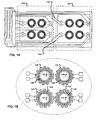
- FIGS. 1A, 1B , 1C and 1D show an example sensor chip device for measuring cell impedance to detect cell migration.
- FIG. 1A shows a fully assembled device 100 that includes two sets 110 and 120 of electrode arrays. Each set of electrode arrays can be implemented in separate chips and then combined together as a single unit. Also, the two sets of electrode arrays can be implemented in a single chip. The two sets 110 and 120 of sensor arrays are connected together using one or more interconnects 130 and 132. Each set 110 and 120 of sensor arrays includes at least one microelectrode sensors, with each electrode sensor including one or more sensing electrodes and a counter electrode.
- FIG. 1C shows a cross section view of an example sensor chip device.
- a sensing electrode 140 is disposed on a substrate 160.
- the electrode 140 is surrounded by insulating material 150. While FIG. 1C shows a single sensing electrode, the device 100 can be implemented using one or more sensing electrodes on a substrate, surrounded by insulating material.
- the insulating material 150 can be the substrate itself or an additional layer on the substrate 160. When two or more sensing electrodes 140 are implemented, each sensing electrode 140 is separated from each other by a gap of insulating material 150.
- FIG. 1B shows examples of sensor arrays for measuring cell impedance.
- Each set of sensor arrays 110 and 120 include multiple sensors.
- FIG. 1B shows four sensors 122, 124, 126, 128.
- the four sensors 122, 124, 126 and 128 represent four sensing units integrated in a sensing chip.
- each set of sensor arrays can include less than four sensors or more than four sensors.
- Each sensor 122, 124, 126, 128 includes multiple sensing electrodes 140 and a counter electrode 123, 125, 127 and 129.
- the sensing electrodes 140 surround the counter electrode 127 in the sensor 126.
- each sensor 122, 124, 126, 128 are arranged as an optimized multi-island array structure.
- This multi-island array structure provides a reliable on-chip cell migration assay.
- each sensor 122, 124, 126, 128 includes 49 round sensing electrodes 140 and a counter electrode 127.
- Each sensing electrode 140 has a diameter of 200 ⁇ m, for example.
- the sensing electrodes 140 surround or encircle one counter electrode (e.g., 123, 125, 127 and 129) in the middle of the sensing electrodes.
- Each sensor 122, 124, 126, 128 can have a diameter of 4mm, for example.
- the sensing electrodes 140 can be positioned to form various geometric shapes around the centrally located counter electrode.
- the sensing electrodes 140 can be arranged to form a circle that surrounds the centrally located counter electrode.
- Each sensing electrode 140 can be located at an equidistance from the centrally located counter.
- each sensing electrode 140 can be separated by equally spaced gaps of insulating materials.
- the sensing electrodes 140 can be arranged to form an oval shape, a square shape, a rectangle, a triangle, etc. to provide a spatially averaged electrical signal from the sensing electrodes 140.
- FIG. 1D is an enlarged view of an example sensor.
- one of the sensors e.g., sensor 1266
- Each sensing electrode 140 is separated from the next sensing electrode 140 by a gap of insulating material 150 as described above.
- the counter electrode 127 is shown to be separated from the sensing electrodes 140.
- the multi-island array structure shown in FIG. 1A-1D can potentially provide one or more of the following advantages.
- the multi-island array structure can provide a more uniform electric field which is beneficial for impedance sensing.
- Each sensing electrode 140 can generate an impedance signal regarding cell migration, so the signal obtained by the device 100 can be an average value for 49 independent repeating electrodes 140. Using the average value can reduce system error.
- the 49 electrodes are arranged around the counter electrode 123, 125, 127 and 129 to produce a spatial average measurement of cell migration. This arrangement can improve the repeatability of the impedance measurement.
- the device 100 includes at least one sensing electrode and one or more counter electrodes.
- Other example arrangements include providing sensing and counter electrodes in ratios of at least 10:1, 20:1, 30:1, 40:1 or 50:1 sensing to counter electrodes.
- the surface area of the counter electrode can designed to be several folds larger than the surface areas of the sensing electrodes.
- the total counter electrode surface area can be at least 1, 2, 10, 20, 40, 80, 100, 200 or 500 times the total surface area of the sensing electrodes.
- microfluidic chambers are fabricated to construct an environment for the cell culture and migration assay.
- the microfluidic chambers can be made of polydimethylsiloxane (PDMS) using a SU-8 technique.
- a mold can be created using SU-8 photoresist on a silicon wafer with a height of 100 ⁇ m, for example.
- PDMS pre-polymer solution base + curing agent in a proportion of 10:1 is poured into the mold and cured in an oven at 72 °C for 2 hours to yield the elastomeric replicas containing the microfluidic chamber.
- the PDMS chamber can be bonded to the glass chip irreversibly after treatment with oxygen plasma generated by a plasma generator (FEMTO, Diener Plasma-Surface-Technology, Germany), and then assembled to the printed circuit board (PCB) by wire bonding.
- FIG. 1A above shows the assembled sensing device, which has a sandwich structure.
- a cell culture cavity is fabricated using soft lithographic techniques. Briefly, polydimethylsiloxane (PDMS) is mixed with cross-linking agent in a proportion of 10:1, poured in the mold made of polymethylmethacrylate (PMMA) and cured in an oven at 72 °C for 3 hours to yield the elastomeric replicas containing the microfluidic channels for cell culture. On the end of each channel, a hole is created for entry of CO 2 throughout in the process of cell culture. A second hole in the middle of the cavity is created for cell seeding and for injection of the cell culture media.
- PDMS polydimethylsiloxane
- PMMA polymethylmethacrylate
- the sensor chip is adhered to the print circuit board (PCB) using epoxy glue, each of the sensor electrodes is soldered to the printed circuit board for electrical connection, and then the PDMS cavity is bonded irreversibly to the sensor chip after treatment with oxygen plasma, forming the integrated cell culture and sensing device.
- PCB print circuit board
- FIG. 2 shows an example process 200 for fabricating a device for measuring cell migration.
- a sensor chip device e.g., device 100
- a conductive layer of Au/Ti Au 200nm and Ti 20 nm
- the conductive layer forms the electrodes (sensing and counter) as described above with respect to FIGS. 1A-1D .
- the sensing electrodes 140 and counter electrodes 123, 125, 127 and 129 can be implemented using any conductive material or combination of conductive materials.
- the electrode surface can include a material on which a thiol SAM can form.
- electrode materials include gold, silver, copper, platinum, iridium, palladium, rhodium, mercury, osmium, ruthenium, gallium arsenide, indium phosphide, mercury cadmium telluride, graphite, conductive polymers and alloys or combination of these. While the example device 100 as described in this specification is produced using gold and/or platinum, the electrodes may be composed of more than one type of metal or alloy. Further, the sensing and counter electrodes can be composed of the same or different materials.
- the surface of the substrate on which the electrodes contact should be non-conductive.
- the substrate may take the form of a foil, a wafer or a chip of the desired material.
- the substrate can include a layer or layers of a non-conductive material in contact with the surface of a substrate.
- the layers or layers of non-conductive material may be referred to as an insulation layer.
- Examples of an insulation layer include SiO 2 /Si 3 N 4 /SiO 2 .
- an insulation layer of SiO 2 /Si 3 N 4 /SiO 2 (400 nm/100 nm/500 nm) is deposited onto the substrate using plasma enhanced chemical vapor deposition (PECVD) (220).
- PECVD plasma enhanced chemical vapor deposition
- the insulation layer on the electrodes (conductive layer) and bonding pads are removed by reactive ion etching (230).
- the impedance detection device as described in this specification can be fabricated using standard lift-off fabrication techniques.
- Pyrex glass wafer e.g., from Coming, New York, 130 NY
- the wafer is then washed with deionized water and dried with nitrogen gas.
- the wafer is coated with SPR6812 photoresist (e.g., from Rohm and Haas, Philadelphia, PA) and then softbaked on a hot plate, for example at 95 for 2 min.
- the photoresist layer is exposed using EV620 (e.g., from EV Group, Austria), and the wafer is baked on a hot plate, for example at 110 for 3 min.
- EV620 e.g., from EV Group, Austria
- a 30 nm thick Ti layer is sputtered on the wafer as an adhesion layer, followed by a 200 nm thick Au layer.
- the electrode pattern is defined by standard photolithographic processes and the wafer is soaked in acetone to remove photoresist and any redundant metal. Finally, the wafer with four independently integrated sensing chips is separated into four chips.
- the chips are adhered to one Printed Circuit Board (PCB) by epoxy glue to form a sensing array.
- the electrodes are connected with the bonding pad on the PCB to make electrical connections with each sensing chip.
- the cell culture cavity of each chip is made from polydimethylsiloxane (PDMS) using soft lithographic techniques and was tightly bonded to the wafer by 02 plasma treatment.
- PDMS polydimethylsiloxane
- PMMA polymethylmethacrylate
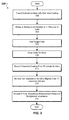
- FIG. 3 shows an example process 300 for measuring cell impedance.
- the surface is treated with a chemical coating that inhibits cell adhesion onto the electrode (302). This generates a chemical coat-modified surface on the electrodes.
- the chemical coating maintains contact with the surface of the electrodes until desorbed by application of an electrical signal capable of desorbing the coating.
- the chemical coating can be applied by contacting the electrodes with a solution or suspension of coating material in a carrier, or by contacting the electrode with the coating material without a carrier.
- a background impedance value is measured in absence of cells (304). After measuring the background impedance (Z0), target cells are added to the device (306). A layer of cells is allowed to grow on the surface of the device (308).
- the added cells do not adhere and grow on the surface of the electrodes. As a result, all the cells grow on the surface of the SiO 2 insulation substrate forming a cell monolayer. After incubation, wound edges are formed automatically on the device. Once the cells have grown over the surfaces, an electrical signal is applied to the electrodes, which causes the chemical coating to desorb from the electrodes (310). This provides a cell-free electrode surface surrounded by cells growing on the adjacent insulation.
- the cell impedance (Z x ) is monitored in real-time as the cells grow or migrate across the electrodes (312).
- the final impedance data is normalized as Z x /Z 0 (314).
- the normalized impedance data reflects the impedance variation induced by the attachment of the cells.
- An example protocol includes preparing an impedance measuring device (e.g., device 100) for impedance measurement by sterilizing the device. After sterilization, (e.g., in 75% ethanol for 20 minutes and then exposure to UV irradiation for another 30 minutes), a thiol compound is added to the microfluidic cavities.
- Thiol compound (HS(CH 2 ) 11 (OCH 2 CH 2 ) 6 OH (abbreviated as "EG6" is obtained from Sigma-Aldrich (St. Louis, MO).
- EG6 (1.5 mM in ethanol) can be added to each microfluidic cavity of the device using a syringe and incubated for 8 hours at room temperature. Then, the microfluidic cavities are washed by ethanol followed by PBS buffer. Before cell seeding, tissue culture media is injected into chambers of the device to read the background impedance value (Z 0 ).
- suspension cells e.g., 2 ⁇ 10 5 cells cm -2
- the device is placed into an incubator for the cell culture and migration assay.
- the SAMs are desorbed from the electrode surface by applying a stimulus signal.
- a DC current (provided by an ordinary DC power supply) can be imposed on the electrodes with an amplitude of 1.5 V for 30 seconds.
- the gold electrodes of the device serves as the cathode, while platinum wire immersed in the culture media serves as the anode.
- the impedance (Z x ) is measured in real-time with a time resolution of 5 minutes, for example.
- the time resolution can be increased to about 5 seconds per measurement.
- the final impedance data is normalized as Z x /Z 0 (310).
- the normalized impedance data reflects the impedance variation induced by the attachment of the cells.
- an AC probe sine signal is applied to the electrodes of the device.
- the cells attach and spread on the surface of sensor electrodes, the cells inhibit the current resulting in a variation of the impedance.
- Measurements can be carried out using a multifunctional data acquisition card NI DAQ PCI-6110 (National Instruments, Austin, TX) controlled by a LabVIEW ® (National Instruments) program, for example.
- the impedance is calculated, recorded and displayed automatically in real time.
- the chemical coating applied to the electrode surface is assembled on the surface of the electrode and not on the surface of the substrate and the surface surrounding the electrode does not have the chemical coating.
- the coating inhibits cell adherence onto the electrode.
- the coating can be desorbed from the electrode upon application of an electrical signal to the electrode.
- the chemical coating applied to the electrode surface can include a SAM.
- Such coating layer is self-assembled because the layer assembles automatically due to attractive forces between the electrode and the coating material.
- a monolayer is produced because the coating must include functional groups that attach to the electrode material. Self-assembled monolayers can be prepared, for example, simply by adding a solution of the desired molecule onto the substrate surface and washing off the excess.
- the monolayer may be formed from a precursor solution or mixture that contains a precursor substance, selected on the basis of coordination chemistry with respect to the precursor and the surface to be coated.
- a precursor substance selected on the basis of coordination chemistry with respect to the precursor and the surface to be coated.
- suitable precursors are n-alkanoic acid, alkyl oxalic acid, hydroxamic acid, phosphonic acid, or sulfate.
- Coordination can be provided between the surface of a gold or platinum with a coating of a thiol, phosphorus or arsenic containing compound. Details of coordination chemistry can be found in U.S. patent 5,523,878 , contents of which are incorporated by reference as a part of this specification.
- the coating of the cell migration device can include a mono- (one molecule thick) or bi- (two molecules thick) layer, or a mixture of a mono- and bi-layer.
- Other examples include a coating composed of a multi- layer (more than two molecules thick).
- the coating may include well-ordered molecules or randomly distributed molecules.
- the coating can selectively maintain contact with the surface of the electrode and not the surface of the substrate. For example, an attractive force between the coating and the surface of the electrode can maintain contact between the coating and the electrode surface. Absence of such attractive force between the coating and the surface of the surrounding substrate or insulation material can prevent application of the coating on the substrate and the insulation layer. Examples of attractive forces include intermolecular forces, such as electrostatic, ionic, van der Waals, H-bonding, covalent bonds, and dipole-dipole interactions.
- the chemical coating can cover various portions of the electrode surface.
- the coating can cover at least 75%, 85%, 95%, or 98% of the surface of the electrode.
- the coating can include a confluent layer that completely covers the surface of the electrode.
- the coating can prevent ells from contacting or adhering to the surface of the electrode until desorbed from the electrode surface.
- the coating can remain on the electrode surface until the electrodes are stimulated with an electrical impulse capable of desorbing the coating.
- the electrical impulse can be characterized by a certain voltage and time applied to the electrode, which is sufficient to desorb all or substantially all of the coating material.
- the coating as described in this specification can be generated using a thiol containing molecule.
- the thiol containing molecule adsorbs through the sulfur (SH) head group to the substrate surface.
- the thiol containing molecule can include a hydrocarbon chain that extends from the surface of the substrate and results in densely packed monolayer films. Descriptions of a thiol containing compound can be found in U.S. patent no. 5,514,501 , the contents of which are incorporated by reference as a part of this specification.
- Dialkyl sulfides correspond to the general formula R(CH 2 ) m S(CH 2 ) n R, and is optionally substituted. Either symmetrical or asymmetrical dialkyl sulfides may be used. Examples of symmetrical dialkyl sulfides include [CH 3 (CH 2 )] 2 S, [HOOC(CH 2 ) n ] 2 S, and [F(CF 2 ) m (CH 2 )] 2 S, each of which may be optionally substituted.
- Examples of asymmetrical dialkyl sulfides include CH 3 (CH 2 ) 9 S(CH 2 ) 10 COOH, CH 3 (CH 2 ) 5 S(CH 2 ) 10 COONa and CH 3 (CH 2 ) 15 S(CH 2 ) 15 COOH, each of which may be optionally substituted.
- Examples of dialkyl disulfide compounds include symmetrical dialkyl disulfides such as [S(CH 2 ) n OH] 2 , [S(CH 2 ) n CH 3 ] 2 , [S(CH 2 ) n Br] 2 , and [S(CH 2 ) n COOH] 2 , each of which may be optionally substituted.
- Asymmetrical dialkyl disulfides may correspond to the formula R(CH 2 ) m S-S(CH 2 ) n R, which may be optionally substituted.
- Each m and n is independently selected from an integer from 0-21.
- Each R is independently selected from a group consisting of H, C1-C20 alkyl, OC1-C20 alkyl, OH, HOOC, NH 2 , CF 3 , and halogen.
- Halogen is defined as bromine, chlorine, iodine, or fluorine.
- the group R includes any functional group that can confer a desired character on the SAM, depending on the intended use. Additional compounds that can form a coating include unsaturated and/or fluorinated versions of the foregoing examples and formulas.
- Alkylene refers to a divalent hydrocarbyl group. Typically it refers to -(CH 2 ) n - where n is 1-21.
- An alkylene can also be substituted by other groups, branched, or of other lengths, and the open valences need not be at opposite ends of a chain.
- -CH(Me)- and -C(Me) 2 - may also be referred to as alkylenes, as can a cyclic group such as cyclopropan-1,1-diyl.
- CaSki , HeLa , Vero-E6 and NIH-3T3 cell lines are obtained from the American Type Culture Collection (ATCC, Manassas, VA). These cells are incubated at 37 °C in a humidified incubator containing 5% CO 2 atmosphere. HeLa and Vero-E6 cell lines are incubated with Dulbecco's modified Eagle's medium supplemented with 10% fetal bovine serum.
- CaSki cell line was maintained with RPMI-1640 media supplemented with 10% fetal bovine serum while NIH-3T3 cell line was incubated with Dulbecco's modified Eagle's medium supplemented with 10% bovine calf serum.
- a monodisperse cell suspension is prepared using standard tissue culture techniques with 0.25% trypsin containing 0.53 mM EDTA.
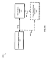
- FIGS. 4A , 4B and 4C show examples of a system 400 for monitoring cell migration.
- the system 400 includes an impedance sensing device 100 in communication with an data analysis system 410 over a bidirectional communication link 420.
- the impedance sensing device 100 can send an output signal that includes cell impedance data measured from the sensing electrodes 140 in the impedance sensing device.
- the data analysis system 410 processes the output signal received from the data analysis system 410 to determine the final impedance data in real-time. For example, signals from the 49 sensing electrodes 140 shown in FIGS. 1A-1D above can be averaged to obtain an averaged impedance measurement.
- the data analysis system 410 can normalize the average data against the background impedance measurement.
- the data analysis device 410 includes an instrument capable of measuring at least one electrical property.
- the data analysis system 410 can process the output data from the impedance sensing device 100 to measure electrical properties, such as impedance, resistance, capacitance, inductance and frequency.
- electrical properties such as impedance, resistance, capacitance, inductance and frequency.
- an instrument that measures impedance include a LCR meter (L is inductance, C is capacitance and R is resistance or impedance).
- the data analysis system 410 can be implemented using one or more data processing devices, such as a desktop computer, a server computer, a portable computer, etc. While FIG. 4A shows only one impedance sensing device 100 in communication with the data analysis system, 410, the analysis device 410 is designed to interface with more than one sensing devices 100. .
- the data analysis system 410 can generate an electrical signal to desorb the coating on the surface of the electrodes.
- the generated electrical signal can be transmitted to the impedance sensing device 100 over the bidirectional communication link 420 to desorb the coating on the surface of the electrodes in the impedance sensing device 100.
- the system 400 can optionally include a power supply / signal generator 420 in communication with the impedance sensing device 100 and/or data analysis system 410 over bidirectional links 422 and/or 424.
- the power supply/signal generator 420 can generate the electrical signal to desorb the coating from the surface of the electrodes.
- the power supply/signal generator sends the generated signal to the impedance sensing device 100 to desorb the coating layer.
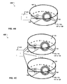
- FIG. 4B shows another example of the system 400 for detecting cell migration.
- a single device 100 is connected to an analysis system 410.
- the device 100 includes gold electrodes 140 fabricated on a glass substrate 160.
- the gold electrodes 140 surround a counter electrode 123, 125, 127 or 129.
- the substrate 160 is adhered onto the bottom of a container 412, such as a petri dish for cell culture.
- FIG. 4C shows yet another example of the system 400 for detecting cell migration.
- multiple devices 100 are connected to the analysis system 410 that measures at least one electrical parameter, e.g., impedance, resistance, capacitance, inductance or frequency.
- the data analysis system 410 can control the sensing device 100 to monitor the impedance measured by the electrodes in real time.
- the data analysis system 410 can control the sensing device 100 to measure a control impedance measurement in absence of cells on the surface of the electrodes. Then, the data analysis system 410 can generate and apply an electrical signal to desorb the coating on the surface of the electrodes. After desorbing the coating, cells will begin to migrate onto the surface of the electrodes.
- the data analysis system 410 can measure the transient impedance at the electrodes as the cells migrate on the surface of the electrodes. This can be achieved by performing real-time monitoring of the impedance after desorbing the coating.
- the change in impedance measurement as the cells migrate onto the surface of the electrode can be processed and analyzed to determine the effects of cell migration on the impedance value.
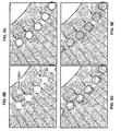
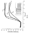
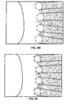
- FIGS. 5A-G illustrate an example of monitoring of cell migration.
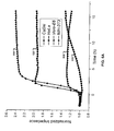
- FIG. 5A shows measured impedance variation for CaSki cells, showing the real-time progress of cell migration.
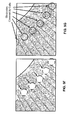
- FIGS. 5B-E show example photographs taken in the progress of cell migration onto the electrodes.
- FIGS. 5F-G show examples fluorescence images of a sensor, showing cell viability after modification of the SAMs and application of the DC current.
- fluorescence dyes calcein-AM and PI is used to label cells and test their viability. Healthy cells present a green fluorescence while dead cells presents a red fluorescence.
- FIGS. 5A-G presents data demonstrating that exemplary devices, systems and techniques described in this specification are effective in providing an artificial wound edge formation, subsequent cell migration monitoring, and cell viability detection.
- FIG. 5B shows that because of the inhibition effect of the SAM-modified gold surface to cell adherence, cells could not adhere and grow on the surface of the gold electrodes treated with a chemical coating. As a result, all the cells grew on the surface of the SiO 2 insulation substrate forming a cell monolayer. After incubation for 24 hours, wound edges are formed automatically on the chip as is shown in FIG. 5B . Once the wound edges in cell monolayer are formed, a 1.5 V DC current is applied to the electrodes for 30 seconds. The SAMs were desorbed from the gold electrodes due to the applied current. With the inhibitory coating gone, the cells start to migrate onto the electrodes, and the progress of cell migration is monitored by the impedance sensing in real-time.
- FIG. 5A shows example impedance data measured for CaSki cell migration on the electrodes after applying an electrical stimulus to remove the SAMs from the electrode surface (510).
- the impedance value increases gradually until leveling off.
- the sharp rise in impedance after the application of a DC current to desorb EG6 from the electrodes indicates cell migration onto the electrodes.
- the time at which the DC current is applied is marked as 'B' and corresponds to FIG. 5B .
- the other time points marked 'C', 'D', and 'E' correspond to FIGS. 5C, 5D and 5E .
- the impedance data as shown on the y-axis represents normalized impedance (Z x /Z 0 ) values.
- the X-axis represents time in hours.
- FIG. 5B wound edges are shown where the chemical coating, such as the thiol compound EG6 is still present on the surface of the electrodes.
- the chemical coating prevents cells from migrating onto the EG6 coating treated electrode surface.
- the EG6 coating is desorbed from the electrode surface and the cells begin to migrate onto the EG6-free electrode surface as shown in FIG. 5C .
- time point D even more cells have migrated onto the electrode surface as shown in FIG. 5D .
- the electrode surface is nearly completely covered by migrating cells as shown in FIG. 5E . This corresponds to the impedance measurements that levels off after the initial rise as shown in FIG. 5A at time E.
- the impedance data shown for control essays (520) are measured without application of a DC current, and thus the SAMs are retained on the electrode surface.
- the normalized impedance value for the control assays does not change over time because in absence of the DC current, the SAMs are retained on the electrode surface.
- the control assays show little evidence of cell migration onto the electrodes.
- FIG. 5F a fluorescence image of the sensor soon after the application of the DC current.
- the cells growing near the edges of the electrodes present a bright green fluorescence without any red color. Red colored cells represent the dead cells. This lack of red color in the cells shows that the applied DC current do not significantly affect the cells adjacent to the electrodes.
- FIG. 5G shows an experimental fluorescence image of the sensor after the application of the DC current and sufficient time has passed for the cells to migrate onto the electrode surface.
- FIG. 5G shows that the cells that have migrated and grown on the round electrodes presented the same bright green fluorescence as the cells that are far away from the electrodes.
- FIG. 5G shows little or no red colored cells representing the dead cells.
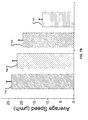
- the cell migration detection devices, techniques and systems described in this specification can be used to effectively quantify and compare the migration speed of cells in real time. For example, using an on-chip cell migration assay, migration of four types of cell lines ( CaSki , HeLa , Vero-E6 and NIH-3T3 ) is monitored in parallel, and the migration speed is measured in real-time. The cells proliferate in the presence of their associated serums, but do not proliferate without the serums. Two groups are prepared: (1) Culture media with 10% serum, where cells can proliferate on the sensing electrodes and cell migration combined with cell proliferation can be detected; (2) Cells starved in serum-free culture media for 12 hours before growing in the serum-free medium, where the cell proliferation independent cell migration can be monitored. FIGS.
- FIG. 6A and 6B show monitored impedance variation for above identified groups (1) and (2) respectively.
- FIG. 6A shows the measured impedance signals for CaSki 620, HeLa 640, Vero-E6 610 and NIH-3T3 630 for group (1).
- FIG. 6B shows the measured impedance signals for CaSki 660, HeLa 680, Vero-E6 650 and NIH-3T3 670 for group (2).
- the impedance value starts to increase in different patterns for the four types of cells. As the cells migrate onto the sensing electrodes, the impedance value increases until all of the sensing electrodes are entirely covered by the cells. This indicates a saturation of the impedance signals.
- t N , t C , t V and t H The time for cells starting to migrate (0 hour) until the cells fully cover the whole sensing electrodes (i.e., the time for wound healing of the cell monolayer) is indicated as t N , t C , t V and t H for the cell types NIH-3T3, CaSki, Vero-E6 and HeLa respectively.
- the saturation value of the impedance is identified as the value at which the impedance curve remains flat and do not increase more than 2% in the next 5 hours.
- the average speed (AS) of cell migration can be calculated according to equation (1).
- AS R ⁇ t - 1 where R is the radius of the sensing electrode (100 ⁇ m).
- FIGS. 6C and 6D show the average speed of the four types of cells migration as calculated according to equation (1) for experimental group (1) and group (2), respectively.
- FIG. 6C shows, the average speed of cell migration for group (1).
- FIG. 6B shows the average speed of cell migration for group (2).
- group 1 the measured speed of cell migration is significantly higher than that in serum-free media (group 2).
- group 2 the average speeds for the cell types NIH-3T3 (672), CaSki (662), Vero-E6 (652) and HeLa (682) in the presence of serum are higher than those in absence of serum (674, 664, 654 and 684).
- CaSki and HeLa cells are both human cervical carcinoma cells, and the migration speed of CaSki is higher than that of HeLa cells.
- Such speed advantage for the CaSki cells over the HeLa cells is present in the serum-containing situation and in the serum-free condition.
- Fibroblast (such as NIH-3T3) cells have a high migration speed, even higher than some cancer cells in the presence of serum. However, in absence of serum, the CaSki cancer cells have the highest average speed.
- Cell migration can be monitored using a chip based assay.
- a migration inhibition assay is performed using a migration inhibition agent colchicine to treat Vero-E6 cells. Normalized impedance values are measured in response to different concentrations of colchicines (e.g., control (0 ⁇ M), 0.1 ⁇ M, 0.2 ⁇ M and 0.4 ⁇ M) and shown as signals 710, 720, 730 and 740 respectively.
- Colchicine inhibits cell migration through disruption of microtubules critical for cell migration and cell motion. The inhibitive effect of colchicine upon Vero-E6 cells can be seen in the impedance curves as shown in FIG. 7AA. The time points a which cell migration reaches saturation are shown as t c , t 0.1 , t 0.2 and t 0.4 respective.
- the DC current is applied to the electrodes and the SAMs are desorbed at a time of 0 hour. Then after a short time, the impedance starts to increase, which implies that the cells have started to migrate onto the surface of sensor electrodes. Higher the concentration of colchicines, slower the increase in impedance.
- This phenomenon also exhibits the inhibitive effect of colchicine upon the speed of Vero-E6 cell migration as shown in FIG. 7B .
- the average speed (AS) of cell migration is calculated according to equation (1) and is shown in FIG. 4B .
- AS average speed
- the inhibition effect of cell migration can be quantified using the parameter AS.
- colchicine inhibits Vero-E6 cell migration in a drug concentration dependant manner.
- FIGS. 8A-E show migration of fibroblast NIH-3T3 cells.
- a DC current is imposed on the counter electrode to desorb the SAMs from the counter electrode in addition to the sensing electrodes.
- some cells also migrated on the edge of the counter electrode.
- the impedance changes resulting from cell attachment on the counter electrode can be neglected without affecting the accuracy of detection results.
- One advantage of this cell migration assay is that retention of cell debris and damaging of cells near the electrode edges can be avoided or minimized.
- Calcein-AM and propidium iodide (PI) were frequently used to test cell viability for the in vitro cell assay.
- Calcein-AM/PI stock solutions were prepared at concentrations of 1 mM/1 mg mL -1 in DMSO/pure water respectively and stored at -20 °C until use. Before usage, cells were washed with PBS buffer and then immersed in a cell culture media containing calcein-AM (10 ⁇ M) and PI (2 ⁇ M) at 37 °C for 20 min. Images were taken using a fluorescence microscope (DM-IRB, Leica, Germany) and a CCD camera (DP-71, Olympus, Japan).
- Pyrex glass wafer can be obtained from Coming Inc. (New York, NY).
- Polydimethylsiloxane (PDMS, Sylgard 184) can be obtained from Dow Coming Inc (Midland, MI).
- SU-8 photoresist can be obtained from Microchem Inc. (Newton, MA).
- Thiol compound (HS(CH 2 ) 11 (OCH 2 CH 2 ) 6 OH (abbreviated as EG6) can be obtained from Sigma-Aldrich (St. Louis, MO).
- Calcein-AM and propidium iodide (PI) can be obtained from Invitrogen (Carlsbad, CA).
- Dulbecco's modified Eagle's medium, RPMI-1640 media, bovine calf serum, fetal bovine serum and trypsin/EDTA solution can be obtained from Gibco BRL Inc. (Grand Island, NY).
- a device for monitoring cell migration can include at least one conductive electrode provide on a surface of the substrate.
- the at least one electrode is surrounded by insulating material.
- the device can be treated to apply a chemical coating to the electrodes after which a layer of cells is allowed to grow on the surface of the device. Once the cells have grown over the surfaces, an electrical signal is applied to the electrodes, which causes the chemical coating to desorb from the electrodes. This provides a cell-free electrode surface surrounded by healthy cells growing on the adjacent insulation.
- the electrodes can then be monitored as the cells grow or migrate across the electrodes. Cells growing on the electrodes cause measurable changes in, e.g., impedance; consequently, cell migration or spreading can be monitored by monitoring electrical properties of the electrodes.
- the stimulation of the electrodes can be applied for a length of time and voltage adequate to desorb greater than 70%, 80%, 90%, 95%, 98% or about 100 % of the coating or cells from the surface of the electrode.
- the coating on the surface of the electrode inhibits positioning of cells onto the surface of the electrode or the surface of the coating. For example, contacting of the cells onto the surface of the electrode or coating is limited to 0%, 2%, 5%, 10%, 25%, 40% or about 50% of the surface area of the electrode or coating.
- the electrode can be stimulated with an electrical signal such that any chemical coating and/or cell is desorbed from the surface electrode.
- the electrical property is impedance, resistance, capacitance, inductance or frequency; and an instrument capable of measuring the property is in communication with the electrodes. In another embodiment, the electrical property is impedance.
- the substrate of the device can include a non-conductive layer or layers on the surface of the substrate.
- the electrode can include one or more sensing electrodes and one or more counter electrodes.
- the counter electrode surface area can be at least 2 times the surface area of the sensing electrodes.
- the device includes at least 10 sensing electrodes an at least one counter electrode.
- the coating can be applied to the sensing electrode alone, counter electrode alone or both. Also, the speed of cell migration can be calculated from the average electrical signals of at least two sensing electrodes. Cell migration can be monitored by measuring the rate at which a cell migrates across a surface. Further, an artificial wound can be created to measure cell migration as a result of the formation of the artificial wound.
- Artificial wound refers to the simulation of an area wherein cells border another area without cells.
- the wound edge refers to the border between the two areas.
- the wound edge may also refer to the nearby region of the border.
- the artificial wound might be created through physical removal of a portion of cells from a cellular colony. It also may be created through prevention of cellular growth, adherence to, or spreading to a particular area.
- the cell migration detection device and techniques described in this specification can be used to probe biological phenomena including embryogenesis, wound healing, inflammatory response and tumor metastasis.
- Cell migration detection is applicable for other technological applications, such as tissue engineering.
- On-chip cell migration assay using self-assembled monolayer chemical modification can be combined with real-time cellular impedance sensing. For example, cell migration can be monitored using quantitative migration data and may be used in a high-throughput and fully-automatic application. In addition, techniques of SAMs and real-time cellular impedance sensing in cell migration assays can be used. Further, the on-chip cell migration assay can be used to evaluate the inhibition effect of potential drugs in real-time which is of benefit for anti-migratory drug screening and drug discovery.
- the cell migration device can be used in a high-throughput screening application.
- high-throughput screening comprises screening a plurality of test compounds for an effect on cellular response.
- High-throughput screening may be carried out in microfluidic devices or micro laboratory systems, which allow for integration of the elements required for performing the assay, automation, and minimal environmental effects on the assay system, e.g., evaporation, contamination, human error.
- Specific configuration of these devices may vary depending upon the type of assay and/or assay orientation desired.
- the screening methods of the invention can be carried out using a micro fluidic device having two intersecting channels.
- multichannel/intersection devices may be employed. The small scale, integratability and self-contained nature of these devices allows for virtually any assay orientation to be realized within the context of the micro laboratory system as described in U.S. patent no. 7,285,411 , the contents of which are.
- deposition of the coating onto the surface of the electrode is performed using the techniques described in U.S. patent 5,523,878 , the contents of which are incorporated by reference. Briefly, the surface of the electrode is cleaned to remove contaminants. This may entail conventional cleaning techniques, using dry processing or solution-based processing. A solution is prepared, which contains the molecular precursor species for the formation of the coating on the surface of the electrode. This solution can be used for liquid deposition of the precursor, which results in the coating of the surface of the electrodes.
- the precursor solution may also contain a solvent for decreasing the surface energy of the solution, with the added benefit that the solvent may be selected so as to remove unwanted residue.
- the precursor solution may contain a surfactant for decreasing surface tension of the solution.
- the precursor solution can be selected to avoid crystallization or aggregation of the precursor molecules, such as perfluorinated solvents.
- perfluorinated solvent include perfluorohexane, PF5060 (Minnesota Mining and Manufacturing Company (3M)), Vertrel XF (Du Pont), and perfluorinated alkanes.
- Coating of the electrode surfaces can include liquid deposition, in which the surfaces to be coated are immersed in or contacted with the precursor solution. In some embodiments, the deposition is performed by immersing the entire device in the solution. However, any method that contacts the precursor solution with at least the surfaces to be coated is suitable.
- the device remains in contact with the precursor solution for a time sufficient to allow the electrode surfaces to be coated or for formation of a self-assembled monolayer.
- the required time can be determined experimentally, and depends on the materials involved.
- the device is left in the precursor solution for at least a period of time sufficient to permit saturation of the surfaces to be coated.
- the coating of the electrode surfaces may be formed by techniques other than immersion. For example, nebulizing the precursor solution and subjecting the surfaces to be coated to the resulting droplets may permit the same self-assembly of the chemical onto the surface of the electrode as immersion.
- the liquid deposition can result in the spontaneous formation of a monolayer. Because of the coordination chemistry between the precursor and the surfaces to be coated, chemical bond formation occurs and anchors the precursor molecules to these surfaces. In some embodiments, the molecules of the precursor solution attempt to occupy every available binding site on the surfaces to which the solution is exposed. Also, removal of the device from contact with the precursor solution may be followed by a rinsing with a solvent to remove excess precursor solution from the surface of the device.
- the coating can include one or more of the above specified formulas.
- the coating compound can be selected to give the coating the ability to form a layer on the surface of the electrode material and to a possess the desired coating properties described above.
- the coating can include a compound containing at least one head group and at least one tail group.
- the head group can include a group that has affinity for the electrode surface. Examples of a head group include -S- or -SH, with both have an affinity to gold.
- the tail group can be hydrophilic, such as -(OCH 2 CH 2 ) 6 -, hydrophobic, such as -(CH 2 ) 11 -, or a mixture of hydrophilic and hydrophobic portions, such as -(CH 2 ) 11 -(OCH 2 CH 2 ) 6 -.
- the coating can include a compound containing at least one head group and at least one tail group.
- the coating can include a thiol containing compound, generally a lipophilic hydrocarbyl group tail group substituted with at least one -SH head group.
- the compound also includes at least one hydrophilic functional group, such as -OH, COOH, or NH 2 .
- the coating comprises a compound selected from the group consisting of R(X)SH, R(X)S(X)S(X)R, R(OX) m SH, R(X)(OX) m SH, and R(XO) m (X)SH; wherein each X is selected from the group consisting of C1-C20 alkylene, C2-C20 alkenylene, and C2-C20 alkynylene; wherein each alkylene, alkenylene and alkynylene may be optionally substituted, fluorinated, branched, cyclic or a combination of these; wherein each R is independently selected from a group consisting of H, C1-C20 alkyl, OC1-C20 alkyl, OH, COOH, NH 2 , CF 3 and halo.
- the coating can include R(C2-C6 alkyleneO) m (C1-C20 alkylene)SH, such as HO(CH 2 CH 2 O) 6 (CH 2 ) 11 SH, or R(C1-C20 alkylene)(OC2-C6 alkylene) m SH.
- m is 0-10.
- m is 3-10.
- m is 4-8.
- the number of carbons in the alkylene, alkenylene or alkynylene may be any desired integer depending on the desired character of the layer to be formed.
- Example compounds can include saturated hydrocarbyl groups having at least 10 carbon atoms and at least one SH group.
- example compounds can include at least 12 carbon atoms, at least one O in an ether linkage, and at least one SH group.
- Monitoring cell migration can include contacting cells on the surface of the device described above; stimulating the electrode with an electrical signal such that any chemical coating and/or cell is desorbed from the electrode surface; and monitoring at least one electrical property of the electrodes over a period of time to allow the cells to migrate and/or grow.
- the cells can be positioned on the surface of the substrate adjacent to the electrode with few or no cells on the surface of the electrode.
- a method of monitoring cell migration described herein may be used in an automated or high-throughput application, wherein at least two said electrodes are distributed over the surface of said substrate.
- a method of cell migration described herein may be used in an automated or high-throughput application, wherein multiple sensing devices can be used simultaneously.
- monitoring of the electrical property is carried out in real time and may be used to calculate the speed of migration of cells on the surface of the electrodes.
- the rate of cell migration is calculated from the average rate of cell migration from sensing electrodes on the device.
Abstract


Description
- This application claims priority under 35 USC §119(a) to Chinese Patent Application No.
CN 200810103526.7, filed on April 8, 2008 - Detection of cell migration is applicable in a variety of biological phenomena such as embryonic development, wound healing and immune response. In these and other applications, cell migration can be detected using various techniques. For example, in wound healing assay, a monolayer of cells are grown on a surface and a portion of cell monolayer is mechanically removed. Then, the scraped area is manually assessed by optical observation using microscopy.
- Techniques, systems and apparatus are described for detecting electrical impedance. In one aspect, a microelectrode sensing device includes a substrate and an array of microelectrode sensors formed on the substrate. Each sensor includes at least one conductive layer formed above the substrate and patterned to include a counter electrode and multiple sensing electrodes to detect an electrical signal in absence and presence of one or more target cells positioned on at least a portion of a surface of each sensing electrode. The sensing electrodes are spaced apart and arranged around the counter electrode to provide a spatially averaged value of the detected electrical signal.
- Implementations can optionally include one or more of the following features. The sensing electrodes can include multiple circular concentric sensing electrodes. The microelectrode sensing device can include one or more layers of insulating material formed between the sensing electrodes to electrically insulate the sensing electrodes from each another. The at least one conductive layer can be patterned to include the counter electrode and the sensing electrodes in a ratio of 1 counter electrode to N sensing electrodes, where N is a positive integer. The at least one conductive layer can be patterned to include the counter electrode and the sensing electrodes so as to provide a total surface area of the counter electrode that is at least twice a total surface area of the sensing electrodes. The at least one conductive layer can be patterned to include the counter electrode and the sensing electrodes to detect a change in the electrical signal in response to the one or more target cells migrating onto the surface of the plurality of sensing electrodes from an area outside of the surface of the sensing electrodes.
- The at least one conductive layer can be patterned to include the counter electrode and the plurality of sensing electrodes to detect an impedance to a flow of the electrical signal in response to the one or more target cells migrating onto the surface of the sensing electrodes from an area outside of the surface of the sensing electrodes. The microelectrode sensing device can include a chemical coating applied on at least a portion of the surface of the sensing electrodes to inhibit adhesion of the one or more target cells onto the surface of the sensing electrodes. The chemical coating can include a self-assembled monolayer or bi-layer. The chemical coating can be made of a material that desorbs from the surface of the sensing electrodes in response to an electrical stimulus. The sensing electrodes can include sensing electrodes arranged to form a concentric shape around the counter electrode located at a center of the concentric shape. The sensing electrodes can be at an equal distance away from each other. Also, each sensing electrode can be at an equal radial distance away from a center of the counter electrode. The sensing electrodes can be symmetrical in shape and similarly sized to provide uniform impedance measurement from one electrode to another.
- In another aspect, a system includes a microelectrode sensing device that includes a substrate, and an array of microelectrode sensors formed on the substrate, each sensor includes at least one conductive layer formed above the substrate and patterned to comprise a counter electrode and multiple sensing electrodes to detect an electrical signal in absence and presence of one or more target cells positioned on at least a portion of a surface of each sensing electrode. The sensing electrodes are spaced apart and arranged around the counter electrode to provide a spatially averaged value of the detected electrical signal. The system also includes an analysis system in communication with the microelectrode sensing device to receive from the microelectrode sensing device data representing at least the electrical signal detected by the sensing electrodes, and process the received data to obtain one or more impedance measurements.
- Implementations can optionally include one or more of the following features. The analysis system can receive the data representing at least the electrical signal detected by the sensing electrodes in absence of the target cells to establish a control impedance measurement. The analysis system can receive in real-time, the data representing at least the electrical signal detected by the sensing electrodes over a period of time corresponding to migration of the one or more target cells onto the surface of the sensing electrodes from a location external to the surface. The analysis system can process the data received in absence of target cells and the data received over the period of time corresponding to migration of the one or more target cells to identify a change in impedance corresponding to the migration of the one or more target cells. The microelectrode sensing device can include a chemical coating on at least a portion of the surface of the plurality of sensing electrodes to inhibit adhesion of the one or more target cells onto the surface of the plurality of sensing electrodes. The chemical coating can include a self-assembled monolayer or bi-layer. The chemical coating can be made of a material that desorbs from the surface of the plurality of sensing electrodes in response to an electrical stimulus. The analysis system is configured to apply the electrical stimulus to the sensing electrodes to desorb the chemical coating.
- In another aspect, a method for monitoring cell migration includes applying a chemical coating layer on at least a portion of a surface of each sensing electrode in a microelectrode sensing device that includes a counter electrode and sensing electrodes to inhibit adhesion of target cells on the surface of each sensing electrode. The target cells are seeded in the microelectrode sensing device to allow the seeded target cells to adhere to areas outside of the surface of each sensing electrode. An electrical signal is applied to each sensing electrode to desorb the applied chemical coating layer from the surface of each sensing electrode. A change is obtained in an electrical impedance measured by each sensing electrode in response to one or more of the seeded target cells migrating onto the surface of each sensing electrode. Implementations can optionally include one or more of the following features. Applying the chemical coating can include applying a layer of thiol based compound. The chemical coating can be applied on a surface of the counter electrode in the microelectrode sensing device. Applying the chemical coating includes applying one or more self-assembled mono layers. A background impedance value can be measured before seeding the target cells. A normalized impedance value can be calculated based on the background impedance value. The change in the electrical impedance in real time can be monitored as the one or more of the seeded target cells migrate onto the surface of each sensing electrode until a steady state impedance is reached. Monitoring the change in the electrical impedance measured by each sensing electrode can include applying another electrical signal to each sensing electrode. Applying the other electrical signal can include in response to the other electrical signal applied to each sensing electrode, receiving a sensed signal from each sensing electrode and averaging the sensed signals to obtain an average impedance measurement due to the one or more of the seeded target cells migrate onto the surface of each sensing electrode.
- In another aspect, a microelectrode sensing device includes a substrate means for providing a base layer. The microelectrode sensing device also includes an array of microelectrode sensing means for sensing electrical signals provided over the substrate. Each sensing means includes at least one conductive layer means for conducting electricity formed above the substrate and patterned to include a counter electrode means and multiple sensing electrode means to detect an electrical signal in absence and presence of one or more target cells positioned on at least a portion of a surface of each sensing electrode. The sensing electrode means are spaced apart and arranged around the counter electrode means to provide a spatially averaged value of the detected electrical signal.
- Implementations can optionally include one or more of the following features. The sensing electrode means can include multiple circular or concentric sensing electrode means. The microelectrode sensing device can include one or more layers of insulating material means for insulating against electricity formed between the sensing electrode means to electrically insulate the sensing electrode means from each another. The at least one conductive layer means can be patterned to include the counter electrode means and the sensing electrode means in a ratio of 1 counter electrode means to N sensing electrode means, where N is a positive integer. The at least one conductive layer means can be patterned to include the counter electrode means and the sensing electrode means so as to provide a total surface area of the counter electrode means that is at least twice a total surface area of the sensing electrode means. The at least one conductive layer means can be patterned to include the counter electrode means and the sensing electrode means to detect a change in the electrical signal in response to the one or more target cells migrating onto the surface of the plurality of sensing electrode means from an area outside of the surface of the sensing electrode means.
- The at least one conductive layer means can be patterned to include the counter electrode means and the plurality of sensing electrode means to detect an impedance to a flow of the electrical signal in response to the one or more target cells migrating onto the surface of the sensing electrode means from an area outside of the surface of the sensing electrode means. The microelectrode sensing device can include a chemical coating means for inhibiting cell adherence applied on at least a portion of the surface of the sensing electrode means to inhibit adhesion of the one or more target cells onto the surface of the sensing electrode means. The chemical coating means can include a self-assembled monolayer or bi-layer. The chemical coating can be made of a material that desorbs from the surface of the sensing electrode means in response to an electrical stimulus. The sensing electrode means can include sensing electrode means arranged to form a concentric shape around the counter electrode means located at a center of the concentric shape. The sensing electrode means can be at an equal distance away from each other. Also, each sensing electrode means can be at an equal radial distance away from a center of the counter electrode means. The sensing electrode means can be symmetrical in shape and similarly sized to provide uniform impedance measurement from one sensing electrode means to another.
- In another aspect, a system includes a microelectrode sensing means that includes a substrate means for providing a base layer, and an array of microelectrode sensor means for providing signal sensing formed on the substrate. Each sensor means includes at least one conductive layer means formed above the substrate means and patterned to comprise a counter electrode means and multiple sensing electrode means to detect an electrical signal in absence and presence of one or more target cells positioned on at least a portion of a surface of each sensing electrode means. The sensing electrode means are spaced apart and arranged around the counter electrode means to provide a spatially averaged value of the detected electrical signal. The system also includes an analysis means in communication with the microelectrode sensing means to receive from the microelectrode sensing means data representing at least the electrical signal detected by the sensing electrode means, and process the received data to obtain one or more impedance measurements.
- Implementations can optionally include one or more of the following features. The analysis means can receive the data representing at least the electrical signal detected by the sensing electrode means in absence of the target cells to establish a control impedance measurement. The analysis means can receive in real-time, the data representing at least the electrical signal detected by the sensing electrode means over a period of time corresponding to migration of the one or more target cells onto the surface of the sensing electrode means from a location external to the surface. The analysis means can process the data received in absence of target cells and the data received over the period of time corresponding to migration of the one or more target cells to identify a change in impedance corresponding to the migration of the one or more target cells. The microelectrode sensing means can include a chemical coating means for inhibiting cell adherence on at least a portion of the surface of the plurality of sensing electrode means to inhibit adhesion of the one or more target cells onto the surface of the plurality of sensing electrode means. The chemical coating means can include a self-assembled monolayer or bi-layer. The chemical coating can be made of a material that desorbs from the surface of the plurality of sensing electrodes in response to an electrical stimulus. The analysis means is configured to apply the electrical stimulus to the sensing electrode means to desorb the chemical coating means.
- The described techniques, systems and apparatus may be implemented in various configurations and operated in ways that can provide one or more of the following advantages. For example, the described assay using surface treatment combined with cellular impedance measurement can be used to eliminate the need for physical removal of the cell monolayer, and thus can avoid damaging the cells near the wound edge. Because there are no (or only minimal) damaged cells in front of the migrating cells, the effect of the damaged cell in detection of the migrating cells can be avoid or minimized. For another example, the detection of cellular impedance can eliminate the time consuming and highly subjective nature of microscopic observation. In addition, the described techniques, systems and apparatus can be used for high-throughput research applications such as anti-migratory drug screening and drug discovery.
-
-
FIGS. 1A, 1B ,1C and 1D show an impedance sensing device for performing cell migration assay. -
FIG. 2 shows anexample process 200 for fabricating a device for measuring cell migration. -
FIG. 3 shows an example process for measuring cell impedance. -
FIGS. 4A ,4B and 4C show examples of a system for monitoring cell migration. -
FIGS. 5A-G illustrate an example application for monitoring cell migration. -
FIGS. 6A ,6B ,6C and 6D show monitored impedance variation for cell migration and cell proliferation. -
FIGS. 7A and7B show and example real time inhibition assay of cell migration. -
FIGS. 8A-E show migration of fibroblast NIH-3T3 cells. - Detection of cell migration is applicable in a wide variety of biological applications such as embryonic development, wound healing and immune response. For example, due to a close relationship between cell migration and cancer metastasis, cell migration has been identified as a target for anti-cancer drug screening and cancer therapy. Cell migration can be detected using various techniques. For example, in wound healing assay, a monolayer of cells is grown on a surface and a portion of cell monolayer is mechanically removed. Recovery of the scraped area is assed by manual optical observation using microscopy. Physical removal of the cell monolayer could damage the cells near the wound edge. These possibly damaged cells in front of the migrating cells can affect the detected result of cell migration. Also, the detection methods based on microscopic can be subjective, time-consuming and strongly dependent on the investigators in determining the number of cells migrated. In addition, the manual and labor-intensive aspects associated with other detection methods may not be suitable for high-throughput research applications such as anti-migratory drug screening and drug discovery.
- Examples of techniques, systems and apparatus are described below for on-chip detection of cell migration using surface treatment and cell impedance measurement. Various implementation techniques can be used to provide automatic impedance sensing for monitoring cell migration, and reliable quantitative measurements.
- A quantitative on-chip cell migration assay can be provided based on surface chemical modification using self-assembled mono layers (SAMs) and cellular impedance sensing. SAMs are used to form wound edges in a cell monolayer followed by cellular impedance sensing to monitor the whole process of cell migration in a real-time, automatic and quantitative manner. SAMs are types of various organic molecules that can align on a surface into two-dimensional, quasi-crystalline domains. SAMs of substituted alkanethiolates (R(C11-C15 alkylene)S-) adsorbed onto the surface of a gold film to inhibit cell adherence can be applied to pattern multiple types of cells within microfluidic channels. SAMs are applied on the surface of each electrode to inhibit cell adherence, forming blank areas in the confluence of a cell monolayer, which is used to mimic the wound in the wound healing migration assay.
- To make the cell migration assay fully automatic and quantitative, the electrical cell-substrate impedance sensing (ECIS) technique is used to quantitatively monitor the progress of cell migration in real-time. ECIS. In ECIS, a weak probe AC electric signal is applied to the electrodes of an ECIS sensing device. When cells migrate and grow on the electrode, the cells physically impede the current resulting in an increase of impedance measured. Thus, ECIS can be used to monitor the process of cell migration. By combing the modified ECIS sensing device with the wound-forming SAMs technique, a real-time, high-throughput, quantitative cell migration monitoring is provided.
-
FIGS. 1A, 1B ,1C and 1D show an example sensor chip device for measuring cell impedance to detect cell migration.FIG. 1A shows a fully assembleddevice 100 that includes twosets sets more interconnects set -
FIG. 1C shows a cross section view of an example sensor chip device. Asensing electrode 140 is disposed on asubstrate 160. Theelectrode 140 is surrounded by insulatingmaterial 150. WhileFIG. 1C shows a single sensing electrode, thedevice 100 can be implemented using one or more sensing electrodes on a substrate, surrounded by insulating material. The insulatingmaterial 150 can be the substrate itself or an additional layer on thesubstrate 160. When two ormore sensing electrodes 140 are implemented, eachsensing electrode 140 is separated from each other by a gap of insulatingmaterial 150. -
FIG. 1B shows examples of sensor arrays for measuring cell impedance. Each set ofsensor arrays FIG. 1B shows foursensors sensors sensor multiple sensing electrodes 140 and acounter electrode sensing electrodes 140 surround thecounter electrode 127 in thesensor 126. - In
FIG. 1B , thesensor FIG. 1B , eachsensor round sensing electrodes 140 and acounter electrode 127. Eachsensing electrode 140 has a diameter of 200 µm, for example. Thesensing electrodes 140 surround or encircle one counter electrode (e.g., 123, 125, 127 and 129) in the middle of the sensing electrodes. Eachsensor - The
sensing electrodes 140 can be positioned to form various geometric shapes around the centrally located counter electrode. For example, thesensing electrodes 140 can be arranged to form a circle that surrounds the centrally located counter electrode. Eachsensing electrode 140 can be located at an equidistance from the centrally located counter. In additional, eachsensing electrode 140 can be separated by equally spaced gaps of insulating materials. In addition to the circular or concentric shape, thesensing electrodes 140 can be arranged to form an oval shape, a square shape, a rectangle, a triangle, etc. to provide a spatially averaged electrical signal from thesensing electrodes 140. -
FIG. 1D is an enlarged view of an example sensor. InFIG. 1D , one of the sensors (e.g., sensor 126) is enlarged to show 5 of thesensing electrodes 140 in thesensor 126. Eachsensing electrode 140 is separated from thenext sensing electrode 140 by a gap of insulatingmaterial 150 as described above. Also, thecounter electrode 127 is shown to be separated from thesensing electrodes 140. - The multi-island array structure shown in
FIG. 1A-1D can potentially provide one or more of the following advantages. For example, the multi-island array structure can provide a more uniform electric field which is beneficial for impedance sensing. Eachsensing electrode 140 can generate an impedance signal regarding cell migration, so the signal obtained by thedevice 100 can be an average value for 49 independent repeatingelectrodes 140. Using the average value can reduce system error. Also, because the speed of cell migration may not be uniform among the 49 sensing electrodes, the 49 electrodes are arranged around thecounter electrode - The example arrangement shown in
FIGS. 1A-1D is provided for illustrated purposes only, and thus other arrangements of the electrodes can be used. In a simple implementation, thedevice 100 includes at least one sensing electrode and one or more counter electrodes. Other example arrangements include providing sensing and counter electrodes in ratios of at least 10:1, 20:1, 30:1, 40:1 or 50:1 sensing to counter electrodes. - In addition, the surface area of the counter electrode can designed to be several folds larger than the surface areas of the sensing electrodes. For example, the total counter electrode surface area can be at least 1, 2, 10, 20, 40, 80, 100, 200 or 500 times the total surface area of the sensing electrodes.
- As shown in
FIGS. 1A-1D , microfluidic chambers are fabricated to construct an environment for the cell culture and migration assay. The microfluidic chambers can be made of polydimethylsiloxane (PDMS) using a SU-8 technique. A mold can be created using SU-8 photoresist on a silicon wafer with a height of 100 µm, for example. Then, PDMS pre-polymer solution (base + curing agent in a proportion of 10:1) is poured into the mold and cured in an oven at 72 °C for 2 hours to yield the elastomeric replicas containing the microfluidic chamber. The PDMS chamber can be bonded to the glass chip irreversibly after treatment with oxygen plasma generated by a plasma generator (FEMTO, Diener Plasma-Surface-Technology, Germany), and then assembled to the printed circuit board (PCB) by wire bonding.FIG. 1A above shows the assembled sensing device, which has a sandwich structure. - An example technique for fabricating cell culture cavity is described as follows. A cell culture cavity is fabricated using soft lithographic techniques. Briefly, polydimethylsiloxane (PDMS) is mixed with cross-linking agent in a proportion of 10:1, poured in the mold made of polymethylmethacrylate (PMMA) and cured in an oven at 72 °C for 3 hours to yield the elastomeric replicas containing the microfluidic channels for cell culture. On the end of each channel, a hole is created for entry of CO2 throughout in the process of cell culture. A second hole in the middle of the cavity is created for cell seeding and for injection of the cell culture media.
- The sensor chip is adhered to the print circuit board (PCB) using epoxy glue, each of the sensor electrodes is soldered to the printed circuit board for electrical connection, and then the PDMS cavity is bonded irreversibly to the sensor chip after treatment with oxygen plasma, forming the integrated cell culture and sensing device.
-
FIG. 2 shows anexample process 200 for fabricating a device for measuring cell migration. A sensor chip device (e.g., device 100) is fabricated using standard semiconductor fabrication techniques. Briefly, a conductive layer of Au/Ti (Au 200nm andTi 20 nm) is sputtered on a glassy substrate, such as cleaned Pyrex glass wafer (210). The conductive layer forms the electrodes (sensing and counter) as described above with respect toFIGS. 1A-1D . Thesensing electrodes 140 andcounter electrodes example device 100 as described in this specification is produced using gold and/or platinum, the electrodes may be composed of more than one type of metal or alloy. Further, the sensing and counter electrodes can be composed of the same or different materials. - The surface of the substrate on which the electrodes contact should be non-conductive. Also, the substrate may take the form of a foil, a wafer or a chip of the desired material.
- The substrate can include a layer or layers of a non-conductive material in contact with the surface of a substrate. The layers or layers of non-conductive material may be referred to as an insulation layer. Examples of an insulation layer include SiO2/Si3N4/SiO2. For example, an insulation layer of SiO2/Si3N4/SiO2 (400 nm/100 nm/500 nm) is deposited onto the substrate using plasma enhanced chemical vapor deposition (PECVD) (220). The insulation layer on the electrodes (conductive layer) and bonding pads are removed by reactive ion etching (230).
- In some implementations, the impedance detection device as described in this specification can be fabricated using standard lift-off fabrication techniques. Pyrex glass wafer (e.g., from Coming, New York, 130 NY) is cleaned for about 15 minutes by the solution composed of H2SO4 and H2O2 (3:1 in volume ratio). The wafer is then washed with deionized water and dried with nitrogen gas. The wafer is coated with SPR6812 photoresist (e.g., from Rohm and Haas, Philadelphia, PA) and then softbaked on a hot plate, for example at 95 for 2 min. The photoresist layer is exposed using EV620 (e.g., from EV Group, Austria), and the wafer is baked on a hot plate, for example at 110 for 3 min. After the formation of the patterned photoresist layer, a 30 nm thick Ti layer is sputtered on the wafer as an adhesion layer, followed by a 200 nm thick Au layer. The electrode pattern is defined by standard photolithographic processes and the wafer is soaked in acetone to remove photoresist and any redundant metal. Finally, the wafer with four independently integrated sensing chips is separated into four chips.
- The chips are adhered to one Printed Circuit Board (PCB) by epoxy glue to form a sensing array. The electrodes are connected with the bonding pad on the PCB to make electrical connections with each sensing chip. The cell culture cavity of each chip is made from polydimethylsiloxane (PDMS) using soft lithographic techniques and was tightly bonded to the wafer by 02 plasma treatment. A flat polymethylmethacrylate (PMMA) plate is placed on the top of PDMS cavity as a lid during cell culture to maintain humidity and sterility.
-
FIG. 3 shows anexample process 300 for measuring cell impedance. For at least one of the electrodes, the surface is treated with a chemical coating that inhibits cell adhesion onto the electrode (302). This generates a chemical coat-modified surface on the electrodes. The chemical coating maintains contact with the surface of the electrodes until desorbed by application of an electrical signal capable of desorbing the coating. The chemical coating can be applied by contacting the electrodes with a solution or suspension of coating material in a carrier, or by contacting the electrode with the coating material without a carrier. A background impedance value is measured in absence of cells (304). After measuring the background impedance (Z0), target cells are added to the device (306). A layer of cells is allowed to grow on the surface of the device (308). Because of the inhibition effect of the chemical coating-modified surface to cell adherence, the added cells do not adhere and grow on the surface of the electrodes. As a result, all the cells grow on the surface of the SiO2 insulation substrate forming a cell monolayer. After incubation, wound edges are formed automatically on the device. Once the cells have grown over the surfaces, an electrical signal is applied to the electrodes, which causes the chemical coating to desorb from the electrodes (310). This provides a cell-free electrode surface surrounded by cells growing on the adjacent insulation. The cell impedance (Zx) is monitored in real-time as the cells grow or migrate across the electrodes (312). Cells growing on the electrodes can cause measurable changes in the electrical properties of the circuit, e.g., impedance; consequently, the rate of cell migration or spreading can be monitored by monitoring electrical properties of the electrodes. The final impedance data is normalized as Zx/Z0 (314). The normalized impedance data reflects the impedance variation induced by the attachment of the cells. - For illustrative purposes, the
process 300 is described using an example protocol for monitoring cell migration. An example protocol includes preparing an impedance measuring device (e.g., device 100) for impedance measurement by sterilizing the device. After sterilization, (e.g., in 75% ethanol for 20 minutes and then exposure to UV irradiation for another 30 minutes), a thiol compound is added to the microfluidic cavities. Thiol compound (HS(CH2)11(OCH2CH2)6OH (abbreviated as "EG6") is obtained from Sigma-Aldrich (St. Louis, MO). EG6 (1.5 mM in ethanol) can be added to each microfluidic cavity of the device using a syringe and incubated for 8 hours at room temperature. Then, the microfluidic cavities are washed by ethanol followed by PBS buffer. Before cell seeding, tissue culture media is injected into chambers of the device to read the background impedance value (Z0). - After measuring the background impedance (Z0), suspension cells (e.g., 2 × 10⁵ cells cm-2) are added to the microfluidic cavities. The device is placed into an incubator for the cell culture and migration assay. The SAMs are desorbed from the electrode surface by applying a stimulus signal. For example, a DC current (provided by an ordinary DC power supply) can be imposed on the electrodes with an amplitude of 1.5 V for 30 seconds. The gold electrodes of the device serves as the cathode, while platinum wire immersed in the culture media serves as the anode.
- At the same time, the impedance (Zx) is measured in real-time with a time resolution of 5 minutes, for example. The time resolution can be increased to about 5 seconds per measurement. The final impedance data is normalized as Zx/Z0 (310). The normalized impedance data reflects the impedance variation induced by the attachment of the cells.
- For impedance sensing, an AC probe sine signal is applied to the electrodes of the device. When cells attach and spread on the surface of sensor electrodes, the cells inhibit the current resulting in a variation of the impedance. Measurements can be carried out using a multifunctional data acquisition card NI DAQ PCI-6110 (National Instruments, Austin, TX) controlled by a LabVIEW® (National Instruments) program, for example. The impedance is calculated, recorded and displayed automatically in real time.
- As described above, the chemical coating applied to the electrode surface is assembled on the surface of the electrode and not on the surface of the substrate and the surface surrounding the electrode does not have the chemical coating. In addition, the coating inhibits cell adherence onto the electrode. Further, the coating can be desorbed from the electrode upon application of an electrical signal to the electrode. The chemical coating applied to the electrode surface can include a SAM. Such coating layer is self-assembled because the layer assembles automatically due to attractive forces between the electrode and the coating material. A monolayer is produced because the coating must include functional groups that attach to the electrode material. Self-assembled monolayers can be prepared, for example, simply by adding a solution of the desired molecule onto the substrate surface and washing off the excess.
- The monolayer may be formed from a precursor solution or mixture that contains a precursor substance, selected on the basis of coordination chemistry with respect to the precursor and the surface to be coated. As a non-limiting example of coordination chemistry, when the surface to be coated includes aluminum, suitable precursors are n-alkanoic acid, alkyl oxalic acid, hydroxamic acid, phosphonic acid, or sulfate. Coordination can be provided between the surface of a gold or platinum with a coating of a thiol, phosphorus or arsenic containing compound. Details of coordination chemistry can be found in
U.S. patent 5,523,878 , contents of which are incorporated by reference as a part of this specification. - In addition, the coating of the cell migration device can include a mono- (one molecule thick) or bi- (two molecules thick) layer, or a mixture of a mono- and bi-layer. Other examples include a coating composed of a multi- layer (more than two molecules thick). Also, the coating may include well-ordered molecules or randomly distributed molecules.
- The coating can selectively maintain contact with the surface of the electrode and not the surface of the substrate. For example, an attractive force between the coating and the surface of the electrode can maintain contact between the coating and the electrode surface. Absence of such attractive force between the coating and the surface of the surrounding substrate or insulation material can prevent application of the coating on the substrate and the insulation layer. Examples of attractive forces include intermolecular forces, such as electrostatic, ionic, van der Waals, H-bonding, covalent bonds, and dipole-dipole interactions.
- The chemical coating can cover various portions of the electrode surface. For example, the coating can cover at least 75%, 85%, 95%, or 98% of the surface of the electrode. Also, the coating can include a confluent layer that completely covers the surface of the electrode.
- The coating can prevent ells from contacting or adhering to the surface of the electrode until desorbed from the electrode surface. For example, the coating can remain on the electrode surface until the electrodes are stimulated with an electrical impulse capable of desorbing the coating. The electrical impulse can be characterized by a certain voltage and time applied to the electrode, which is sufficient to desorb all or substantially all of the coating material.
- The coating as described in this specification can be generated using a thiol containing molecule. The thiol containing molecule adsorbs through the sulfur (SH) head group to the substrate surface. The thiol containing molecule can include a hydrocarbon chain that extends from the surface of the substrate and results in densely packed monolayer films. Descriptions of a thiol containing compound can be found in
U.S. patent no. 5,514,501 , the contents of which are incorporated by reference as a part of this specification. - Other types of compounds that can produce alkylthiolate mono layers include dialkyl sulfides and dialkyl disulfides. Dialkyl sulfides correspond to the general formula R(CH2)mS(CH2)nR, and is optionally substituted. Either symmetrical or asymmetrical dialkyl sulfides may be used. Examples of symmetrical dialkyl sulfides include [CH3(CH2)]2S, [HOOC(CH2)n]2S, and [F(CF2)m(CH2)]2S, each of which may be optionally substituted. Examples of asymmetrical dialkyl sulfides include CH3(CH2)9S(CH2)10COOH, CH3(CH2)5S(CH2)10COONa and CH3(CH2)15S(CH2)15COOH, each of which may be optionally substituted. Examples of dialkyl disulfide compounds include symmetrical dialkyl disulfides such as [S(CH2)nOH]2, [S(CH2)nCH3]2, [S(CH2)nBr]2, and [S(CH2)nCOOH]2, each of which may be optionally substituted. Asymmetrical dialkyl disulfides may correspond to the formula R(CH2)mS-S(CH2)nR, which may be optionally substituted. Each m and n is independently selected from an integer from 0-21. Each R is independently selected from a group consisting of H, C1-C20 alkyl, OC1-C20 alkyl, OH, HOOC, NH2, CF3, and halogen. Halogen is defined as bromine, chlorine, iodine, or fluorine. In some embodiments, the group R includes any functional group that can confer a desired character on the SAM, depending on the intended use. Additional compounds that can form a coating include unsaturated and/or fluorinated versions of the foregoing examples and formulas.
- Optional substituents may include C1-C8 alkyl, C1-C8 alkenyl, C1-C8 alkynyl, C1-C8 heteroalkyl, halo, CN, COOR, =O, =NR, =NOR, =N-CN, OR, or NR2, wherein each R is independently H, C1-C6 alkyl, or C1-C6 heteroalkyl, and wherein two R can optionally cyclize to form a 3-7 membered ring containing 0-2 heteroatoms selected from N, O and S.
- Alkylene as used herein refers to a divalent hydrocarbyl group. Typically it refers to -(CH2)n- where n is 1-21. An alkylene can also be substituted by other groups, branched, or of other lengths, and the open valences need not be at opposite ends of a chain. Thus, -CH(Me)- and -C(Me)2- may also be referred to as alkylenes, as can a cyclic group such as cyclopropan-1,1-diyl.
- Various techniques can be used to introduce cells onto the cell migration detecting device described in this specification. For example, CaSki, HeLa, Vero-E6 and NIH-3T3 cell lines are obtained from the American Type Culture Collection (ATCC, Manassas, VA). These cells are incubated at 37 °C in a humidified incubator containing 5% CO2 atmosphere. HeLa and Vero-E6 cell lines are incubated with Dulbecco's modified Eagle's medium supplemented with 10% fetal bovine serum. CaSki cell line was maintained with RPMI-1640 media supplemented with 10% fetal bovine serum while NIH-3T3 cell line was incubated with Dulbecco's modified Eagle's medium supplemented with 10% bovine calf serum. For seeding cells onto the sensors, a monodisperse cell suspension is prepared using standard tissue culture techniques with 0.25% trypsin containing 0.53 mM EDTA.
-
FIGS. 4A ,4B and 4C show examples of asystem 400 for monitoring cell migration. As shown inFIG. 4A , thesystem 400 includes animpedance sensing device 100 in communication with andata analysis system 410 over abidirectional communication link 420. Theimpedance sensing device 100 can send an output signal that includes cell impedance data measured from thesensing electrodes 140 in the impedance sensing device. Thedata analysis system 410 processes the output signal received from thedata analysis system 410 to determine the final impedance data in real-time. For example, signals from the 49sensing electrodes 140 shown inFIGS. 1A-1D above can be averaged to obtain an averaged impedance measurement. Thedata analysis system 410 can normalize the average data against the background impedance measurement. - The
data analysis device 410 includes an instrument capable of measuring at least one electrical property. For example, thedata analysis system 410 can process the output data from theimpedance sensing device 100 to measure electrical properties, such as impedance, resistance, capacitance, inductance and frequency. Examples of an instrument that measures impedance include a LCR meter (L is inductance, C is capacitance and R is resistance or impedance). In addition, thedata analysis system 410 can be implemented using one or more data processing devices, such as a desktop computer, a server computer, a portable computer, etc. WhileFIG. 4A shows only oneimpedance sensing device 100 in communication with the data analysis system, 410, theanalysis device 410 is designed to interface with more than onesensing devices 100. . - In addition, the
data analysis system 410 can generate an electrical signal to desorb the coating on the surface of the electrodes. The generated electrical signal can be transmitted to theimpedance sensing device 100 over thebidirectional communication link 420 to desorb the coating on the surface of the electrodes in theimpedance sensing device 100. - The
system 400 can optionally include a power supply /signal generator 420 in communication with theimpedance sensing device 100 and/ordata analysis system 410 overbidirectional links 422 and/or 424. Instead of thedata analysis system 410, the power supply/signal generator 420 can generate the electrical signal to desorb the coating from the surface of the electrodes. The power supply/signal generator sends the generated signal to theimpedance sensing device 100 to desorb the coating layer. -
FIG. 4B shows another example of thesystem 400 for detecting cell migration. In this example, asingle device 100 is connected to ananalysis system 410. Thedevice 100 includesgold electrodes 140 fabricated on aglass substrate 160. Thegold electrodes 140 surround acounter electrode substrate 160 is adhered onto the bottom of a container 412, such as a petri dish for cell culture. -
FIG. 4C shows yet another example of thesystem 400 for detecting cell migration. In this example,multiple devices 100 are connected to theanalysis system 410 that measures at least one electrical parameter, e.g., impedance, resistance, capacitance, inductance or frequency. - In addition, the
data analysis system 410 can control thesensing device 100 to monitor the impedance measured by the electrodes in real time. For example, thedata analysis system 410 can control thesensing device 100 to measure a control impedance measurement in absence of cells on the surface of the electrodes. Then, thedata analysis system 410 can generate and apply an electrical signal to desorb the coating on the surface of the electrodes. After desorbing the coating, cells will begin to migrate onto the surface of the electrodes. Thedata analysis system 410 can measure the transient impedance at the electrodes as the cells migrate on the surface of the electrodes. This can be achieved by performing real-time monitoring of the impedance after desorbing the coating. The change in impedance measurement as the cells migrate onto the surface of the electrode can be processed and analyzed to determine the effects of cell migration on the impedance value. -
FIGS. 5A-G illustrate an example of monitoring of cell migration.FIG. 5A shows measured impedance variation for CaSki cells, showing the real-time progress of cell migration.FIGS. 5B-E show example photographs taken in the progress of cell migration onto the electrodes.FIGS. 5F-G show examples fluorescence images of a sensor, showing cell viability after modification of the SAMs and application of the DC current. In order to evaluate the potential influence to the cell viability, especially to the cells on the edges of the electrodes, fluorescence dyes calcein-AM and PI is used to label cells and test their viability. Healthy cells present a green fluorescence while dead cells presents a red fluorescence. - The example cell migration shown in
FIGS. 5A-G presents data demonstrating that exemplary devices, systems and techniques described in this specification are effective in providing an artificial wound edge formation, subsequent cell migration monitoring, and cell viability detection. -
FIG. 5B shows that because of the inhibition effect of the SAM-modified gold surface to cell adherence, cells could not adhere and grow on the surface of the gold electrodes treated with a chemical coating. As a result, all the cells grew on the surface of the SiO2 insulation substrate forming a cell monolayer. After incubation for 24 hours, wound edges are formed automatically on the chip as is shown inFIG. 5B . Once the wound edges in cell monolayer are formed, a 1.5 V DC current is applied to the electrodes for 30 seconds. The SAMs were desorbed from the gold electrodes due to the applied current. With the inhibitory coating gone, the cells start to migrate onto the electrodes, and the progress of cell migration is monitored by the impedance sensing in real-time. -
FIG. 5A shows example impedance data measured for CaSki cell migration on the electrodes after applying an electrical stimulus to remove the SAMs from the electrode surface (510). For example, in response to an application of the electrical stimulus that includes a DC current applied at a time of 0 hour, the impedance value increases gradually until leveling off. The sharp rise in impedance after the application of a DC current to desorb EG6 from the electrodes indicates cell migration onto the electrodes. The time at which the DC current is applied is marked as 'B' and corresponds toFIG. 5B . The other time points marked 'C', 'D', and 'E' correspond toFIGS. 5C, 5D and 5E . The impedance data as shown on the y-axis represents normalized impedance (Zx/Z0) values. The X-axis represents time in hours. - In
FIG. 5B , wound edges are shown where the chemical coating, such as the thiol compound EG6 is still present on the surface of the electrodes. The chemical coating prevents cells from migrating onto the EG6 coating treated electrode surface. When the DC current is applied, the EG6 coating is desorbed from the electrode surface and the cells begin to migrate onto the EG6-free electrode surface as shown inFIG. 5C . At time point D, even more cells have migrated onto the electrode surface as shown inFIG. 5D . At time point E, the electrode surface is nearly completely covered by migrating cells as shown inFIG. 5E . This corresponds to the impedance measurements that levels off after the initial rise as shown inFIG. 5A at time E. - Thus, these microscopic photographs validate the relationship between impedance variation and cell migration.
- Referring back to
FIG. 5A , the impedance data shown for control essays (520) are measured without application of a DC current, and thus the SAMs are retained on the electrode surface. In contrast to the application of the DC current, the normalized impedance value for the control assays does not change over time because in absence of the DC current, the SAMs are retained on the electrode surface. Thus, the control assays show little evidence of cell migration onto the electrodes. - After the DC current is applied to the electrodes, calcein-AM combined with PI is used to test the influence of the DC current upon the viability of the cells. The experimental result is shown in
FIG. 5F , a fluorescence image of the sensor soon after the application of the DC current. InFIG. 5F , the cells growing near the edges of the electrodes present a bright green fluorescence without any red color. Red colored cells represent the dead cells. This lack of red color in the cells shows that the applied DC current do not significantly affect the cells adjacent to the electrodes. - After the DC current effectively desorbed the SAMs from the gold electrodes, the influence of the modified electrodes upon cell viability is evaluated using fluorescence dyes.
FIG. 5G shows an experimental fluorescence image of the sensor after the application of the DC current and sufficient time has passed for the cells to migrate onto the electrode surface.FIG. 5G shows that the cells that have migrated and grown on the round electrodes presented the same bright green fluorescence as the cells that are far away from the electrodes.FIG. 5G shows little or no red colored cells representing the dead cells. - The cell migration detection devices, techniques and systems described in this specification can be used to effectively quantify and compare the migration speed of cells in real time. For example, using an on-chip cell migration assay, migration of four types of cell lines (CaSki, HeLa, Vero-E6 and NIH-3T3) is monitored in parallel, and the migration speed is measured in real-time. The cells proliferate in the presence of their associated serums, but do not proliferate without the serums. Two groups are prepared: (1) Culture media with 10% serum, where cells can proliferate on the sensing electrodes and cell migration combined with cell proliferation can be detected; (2) Cells starved in serum-free culture media for 12 hours before growing in the serum-free medium, where the cell proliferation independent cell migration can be monitored.
FIGS. 6A and6B show monitored impedance variation for above identified groups (1) and (2) respectively. For example,FIG. 6A shows the measured impedance signals forCaSki 620,HeLa 640, Vero-E6 610 and NIH-3T3 630 for group (1).FIG. 6B shows the measured impedance signals forCaSki 660,HeLa 680, Vero-E6 650 and NIH-3T3 670 for group (2). - In
FIGS. 6A and6B , after a DC current is applied and SAMs are desorbed from the electrodes, the impedance value starts to increase in different patterns for the four types of cells. As the cells migrate onto the sensing electrodes, the impedance value increases until all of the sensing electrodes are entirely covered by the cells. This indicates a saturation of the impedance signals. - The time for cells starting to migrate (0 hour) until the cells fully cover the whole sensing electrodes (i.e., the time for wound healing of the cell monolayer) is indicated as tN, tC, tV and tH for the cell types NIH-3T3, CaSki, Vero-E6 and HeLa respectively.
- In determining these time periods, the saturation value of the impedance is identified as the value at which the impedance curve remains flat and do not increase more than 2% in the next 5 hours. At this point in time, the measurement of cell migration can be stopped. The average speed (AS) of cell migration can be calculated according to equation (1).

where R is the radius of the sensing electrode (100 µm).FIGS. 6C and 6D show the average speed of the four types of cells migration as calculated according to equation (1) for experimental group (1) and group (2), respectively. -
FIG. 6C shows, the average speed of cell migration for group (1).FIG. 6B shows the average speed of cell migration for group (2). Because of cell proliferation in the presence of serum (group 1), the measured speed of cell migration is significantly higher than that in serum-free media (group 2). For example, the average speeds for the cell types NIH-3T3 (672), CaSki (662), Vero-E6 (652) and HeLa (682) in the presence of serum are higher than those in absence of serum (674, 664, 654 and 684). Thus, quantitative data on the effect of serum on cell migration speed can be provided. - CaSki and HeLa cells are both human cervical carcinoma cells, and the migration speed of CaSki is higher than that of HeLa cells. Such speed advantage for the CaSki cells over the HeLa cells is present in the serum-containing situation and in the serum-free condition. Fibroblast (such as NIH-3T3) cells have a high migration speed, even higher than some cancer cells in the presence of serum. However, in absence of serum, the CaSki cancer cells have the highest average speed.
- Cell migration can be monitored using a chip based assay. A migration inhibition assay is performed using a migration inhibition agent colchicine to treat Vero-E6 cells. Normalized impedance values are measured in response to different concentrations of colchicines (e.g., control (0 µM), 0.1 µM, 0.2 µM and 0.4 µM) and shown as
signals - In
FIG. 7(A) , the DC current is applied to the electrodes and the SAMs are desorbed at a time of 0 hour. Then after a short time, the impedance starts to increase, which implies that the cells have started to migrate onto the surface of sensor electrodes. Higher the concentration of colchicines, slower the increase in impedance. The time points at which the cells heal a wound for different situations include tc = 4.2 ± 0.17 h (control), t0.1 = 4.6 ± 0.19 h (0.1 µM colchicine), t0.2 = 5.1 ± 0.21 h (0.2 µM colchicine) and t0.4 = 8.2 ± 0.42 h (0.4 µM colchicine). These time points represents the times at which the increase in the impedance saturates to indicate near complete migration of cells onto the electrode surface. - This phenomenon also exhibits the inhibitive effect of colchicine upon the speed of Vero-E6 cell migration as shown in
FIG. 7B . The average speed (AS) of cell migration is calculated according to equation (1) and is shown inFIG. 4B . Using this quantitative on-chip cell migration assay, the inhibition effect of cell migration can be quantified using the parameter AS. For example, colchicine inhibits Vero-E6 cell migration in a drug concentration dependant manner. -
FIGS. 8A-E show migration of fibroblast NIH-3T3 cells. In this example, a DC current is imposed on the counter electrode to desorb the SAMs from the counter electrode in addition to the sensing electrodes. In response to the desportion of the SAM from the counter electrode, some cells also migrated on the edge of the counter electrode. However, because the total surface area of the counter electrode is made much larger than that of the sensing electrodes, the impedance changes resulting from cell attachment on the counter electrode can be neglected without affecting the accuracy of detection results. - One advantage of this cell migration assay is that retention of cell debris and damaging of cells near the electrode edges can be avoided or minimized.
- Calcein-AM and propidium iodide (PI) were frequently used to test cell viability for the in vitro cell assay. Calcein-AM/PI stock solutions were prepared at concentrations of 1 mM/1 mg mL-1 in DMSO/pure water respectively and stored at -20 °C until use. Before usage, cells were washed with PBS buffer and then immersed in a cell culture media containing calcein-AM (10 µM) and PI (2 µM) at 37 °C for 20 min. Images were taken using a fluorescence microscope (DM-IRB, Leica, Germany) and a CCD camera (DP-71, Olympus, Japan).
- Pyrex glass wafer can be obtained from Coming Inc. (New York, NY). Polydimethylsiloxane (PDMS, Sylgard 184) can be obtained from Dow Coming Inc (Midland, MI). SU-8 photoresist can be obtained from Microchem Inc. (Newton, MA). Thiol compound (HS(CH2)11(OCH2CH2)6OH (abbreviated as EG6) can be obtained from Sigma-Aldrich (St. Louis, MO). Calcein-AM and propidium iodide (PI) can be obtained from Invitrogen (Carlsbad, CA). Dulbecco's modified Eagle's medium, RPMI-1640 media, bovine calf serum, fetal bovine serum and trypsin/EDTA solution can be obtained from Gibco BRL Inc. (Grand Island, NY).
- Only a few implementations have been described. The techniques, systems and apparatus for detecting migration are applicable in additional implementations. A device for monitoring cell migration can include at least one conductive electrode provide on a surface of the substrate. The at least one electrode is surrounded by insulating material. The device can be treated to apply a chemical coating to the electrodes after which a layer of cells is allowed to grow on the surface of the device. Once the cells have grown over the surfaces, an electrical signal is applied to the electrodes, which causes the chemical coating to desorb from the electrodes. This provides a cell-free electrode surface surrounded by healthy cells growing on the adjacent insulation. The electrodes can then be monitored as the cells grow or migrate across the electrodes. Cells growing on the electrodes cause measurable changes in, e.g., impedance; consequently, cell migration or spreading can be monitored by monitoring electrical properties of the electrodes.
- Cell contact or adherence on the surface of the electrode is inhibited or reduced by the coating applied on the electrode surface. The stimulation of the electrodes can be applied for a length of time and voltage adequate to desorb greater than 70%, 80%, 90%, 95%, 98% or about 100 % of the coating or cells from the surface of the electrode. The coating on the surface of the electrode inhibits positioning of cells onto the surface of the electrode or the surface of the coating. For example, contacting of the cells onto the surface of the electrode or coating is limited to 0%, 2%, 5%, 10%, 25%, 40% or about 50% of the surface area of the electrode or coating. The electrode can be stimulated with an electrical signal such that any chemical coating and/or cell is desorbed from the surface electrode. In other embodiments, the electrical property is impedance, resistance, capacitance, inductance or frequency; and an instrument capable of measuring the property is in communication with the electrodes. In another embodiment, the electrical property is impedance.
- The substrate of the device can include a non-conductive layer or layers on the surface of the substrate. The electrode can include one or more sensing electrodes and one or more counter electrodes. The counter electrode surface area can be at least 2 times the surface area of the sensing electrodes. In some embodiments, the device includes at least 10 sensing electrodes an at least one counter electrode.
- The coating can be applied to the sensing electrode alone, counter electrode alone or both. Also, the speed of cell migration can be calculated from the average electrical signals of at least two sensing electrodes. Cell migration can be monitored by measuring the rate at which a cell migrates across a surface. Further, an artificial wound can be created to measure cell migration as a result of the formation of the artificial wound.
- Artificial wound refers to the simulation of an area wherein cells border another area without cells. The wound edge refers to the border between the two areas. The wound edge may also refer to the nearby region of the border. The artificial wound might be created through physical removal of a portion of cells from a cellular colony. It also may be created through prevention of cellular growth, adherence to, or spreading to a particular area.
- The cell migration detection device and techniques described in this specification can be used to probe biological phenomena including embryogenesis, wound healing, inflammatory response and tumor metastasis. Cell migration detection is applicable for other technological applications, such as tissue engineering.
- On-chip cell migration assay using self-assembled monolayer chemical modification can be combined with real-time cellular impedance sensing. For example, cell migration can be monitored using quantitative migration data and may be used in a high-throughput and fully-automatic application. In addition, techniques of SAMs and real-time cellular impedance sensing in cell migration assays can be used. Further, the on-chip cell migration assay can be used to evaluate the inhibition effect of potential drugs in real-time which is of benefit for anti-migratory drug screening and drug discovery.
- The cell migration device can be used in a high-throughput screening application. In one embodiment, high-throughput screening comprises screening a plurality of test compounds for an effect on cellular response. High-throughput screening may be carried out in microfluidic devices or micro laboratory systems, which allow for integration of the elements required for performing the assay, automation, and minimal environmental effects on the assay system, e.g., evaporation, contamination, human error. Specific configuration of these devices may vary depending upon the type of assay and/or assay orientation desired. For example, in some embodiments, the screening methods of the invention can be carried out using a micro fluidic device having two intersecting channels. For more complex assays or assay orientations, multichannel/intersection devices may be employed. The small scale, integratability and self-contained nature of these devices allows for virtually any assay orientation to be realized within the context of the micro laboratory system as described in
U.S. patent no. 7,285,411 , the contents of which are. - In some implementations, deposition of the coating onto the surface of the electrode is performed using the techniques described in
U.S. patent 5,523,878 , the contents of which are incorporated by reference. Briefly, the surface of the electrode is cleaned to remove contaminants. This may entail conventional cleaning techniques, using dry processing or solution-based processing. A solution is prepared, which contains the molecular precursor species for the formation of the coating on the surface of the electrode. This solution can be used for liquid deposition of the precursor, which results in the coating of the surface of the electrodes. The precursor solution may also contain a solvent for decreasing the surface energy of the solution, with the added benefit that the solvent may be selected so as to remove unwanted residue. In addition, the precursor solution may contain a surfactant for decreasing surface tension of the solution. The precursor solution can be selected to avoid crystallization or aggregation of the precursor molecules, such as perfluorinated solvents. Examples of a perfluorinated solvent include perfluorohexane, PF5060 (Minnesota Mining and Manufacturing Company (3M)), Vertrel XF (Du Pont), and perfluorinated alkanes. Coating of the electrode surfaces can include liquid deposition, in which the surfaces to be coated are immersed in or contacted with the precursor solution. In some embodiments, the deposition is performed by immersing the entire device in the solution. However, any method that contacts the precursor solution with at least the surfaces to be coated is suitable. The device remains in contact with the precursor solution for a time sufficient to allow the electrode surfaces to be coated or for formation of a self-assembled monolayer. The required time can be determined experimentally, and depends on the materials involved. In general, the device is left in the precursor solution for at least a period of time sufficient to permit saturation of the surfaces to be coated. The coating of the electrode surfaces may be formed by techniques other than immersion. For example, nebulizing the precursor solution and subjecting the surfaces to be coated to the resulting droplets may permit the same self-assembly of the chemical onto the surface of the electrode as immersion. - The liquid deposition can result in the spontaneous formation of a monolayer. Because of the coordination chemistry between the precursor and the surfaces to be coated, chemical bond formation occurs and anchors the precursor molecules to these surfaces. In some embodiments, the molecules of the precursor solution attempt to occupy every available binding site on the surfaces to which the solution is exposed. Also, removal of the device from contact with the precursor solution may be followed by a rinsing with a solvent to remove excess precursor solution from the surface of the device.
- In addition to the chemical compounds described above many other compounds can be used. The coating can include one or more of the above specified formulas. The coating compound can be selected to give the coating the ability to form a layer on the surface of the electrode material and to a possess the desired coating properties described above.
- For example, the coating can include a compound containing at least one head group and at least one tail group. The head group can include a group that has affinity for the electrode surface. Examples of a head group include -S- or -SH, with both have an affinity to gold. Also, the tail group can be hydrophilic, such as -(OCH2CH2)6-, hydrophobic, such as -(CH2)11-, or a mixture of hydrophilic and hydrophobic portions, such as -(CH2)11-(OCH2CH2)6-.
- In some embodiments, the coating can include a compound containing at least one head group and at least one tail group. Also, the coating can include a thiol containing compound, generally a lipophilic hydrocarbyl group tail group substituted with at least one -SH head group. The compound also includes at least one hydrophilic functional group, such as -OH, COOH, or NH2.
- In some embodiments, the coating comprises a compound selected from the group consisting of
R(X)SH,
R(X)S(X)S(X)R,
R(OX)mSH,
R(X)(OX)mSH,
and R(XO)m(X)SH;
wherein each X is selected from the group consisting of C1-C20 alkylene, C2-C20 alkenylene, and C2-C20 alkynylene; wherein each alkylene, alkenylene and alkynylene may be optionally substituted, fluorinated, branched, cyclic or a combination of these; wherein each R is independently selected from a group consisting of H, C1-C20 alkyl, OC1-C20 alkyl, OH, COOH, NH2, CF3 and halo. - The coating can include R(C2-C6 alkyleneO)m(C1-C20 alkylene)SH, such as HO(CH2CH2O)6(CH2)11SH, or R(C1-C20 alkylene)(OC2-C6 alkylene)mSH. In some embodiments, m is 0-10. In other embodiments, m is 3-10. In yet other embodiments, m is 4-8. The number of carbons in the alkylene, alkenylene or alkynylene may be any desired integer depending on the desired character of the layer to be formed. Example compounds can include saturated hydrocarbyl groups having at least 10 carbon atoms and at least one SH group. Also example compounds can include at least 12 carbon atoms, at least one O in an ether linkage, and at least one SH group. Monitoring cell migration can include contacting cells on the surface of the device described above; stimulating the electrode with an electrical signal such that any chemical coating and/or cell is desorbed from the electrode surface; and monitoring at least one electrical property of the electrodes over a period of time to allow the cells to migrate and/or grow. The cells can be positioned on the surface of the substrate adjacent to the electrode with few or no cells on the surface of the electrode.
- In alternative embodiments, a method of monitoring cell migration described herein may be used in an automated or high-throughput application, wherein at least two said electrodes are distributed over the surface of said substrate. In alternative embodiments, a method of cell migration described herein may be used in an automated or high-throughput application, wherein multiple sensing devices can be used simultaneously. In alternative embodiments, monitoring of the electrical property is carried out in real time and may be used to calculate the speed of migration of cells on the surface of the electrodes. In some embodiments, the rate of cell migration is calculated from the average rate of cell migration from sensing electrodes on the device.
- While this specification contains many specifics, these should not be construed as limitations on the scope of any invention or of what may be claimed, but rather as descriptions of features that may be specific to particular embodiments of particular inventions. Certain features that are described in this specification in the context of separate embodiments can also be implemented in combination in a single embodiment. Conversely, various features that are described in the context of a single embodiment can also be implemented in multiple embodiments separately or in any suitable subcombination. Moreover, although features may be described above as acting in certain combinations and even initially claimed as such, one or more features from a claimed combination can in some cases be excised from the combination, and the claimed combination may be directed to a subcombination or variation of a subcombination.
- Similarly, while operations are depicted in the drawings in a particular order, this should not be understood as requiring that such operations be performed in the particular order shown or in sequential order, or that all illustrated operations be performed, to achieve desirable results. Moreover, the separation of various system components in the embodiments described above should not be understood as requiring such separation in all embodiments.
- Only a few implementations and examples are described and other implementations, enhancements and variations can be made based on what is described and illustrated in this application.
Claims (16)
- A method for monitoring cell migration comprising:applying a chemical coating layer on at least a portion of a surface of each sensing electrode in a microelectrode sensing device that includes a counter electrode and a plurality of sensing electrodes to inhibit adhesion of target cells on the surface of each sensing electrode; seeding the target cells in the microelectrode sensing device to allow the seeded target cells to adhere to areas outside of the surface of each sensing electrode;applying an electrical signal to each sensing electrode to desorb the applied chemical coating layer from the surface of each sensing electrode; anddetecting a change in an electrical impedance measured by each sensing electrode in response to one or more of the seeded target cells migrating onto the surface of each sensing electrode.
- The method of claim 1, wherein applying the chemical coating comprises applying a layer of thiol based compound.
- The method of claim 1, further comprising applying the chemical coating on a surface of the counter electrode in the microelectrode sensing device.
- The method of claim 1, wherein applying the chemical coating comprise applying one or more self-assembled monolayers.
- The method of claim 1, comprising measuring a background impedance value before seeding the target cells.
- The method of claim 5, comprising calculating a normalized impedance value based on the background impedance value.
- The method of claim 1, comprising detecting the change in the electrical impedance in real time as the one or more of the seeded target cells migrate onto the surface of each sensing electrode until a steady state impedance is reached.
- The method of claim 1, wherein detecting the change in the electrical impedance measured by each sensing electrode comprises applying another electrical signal to each sensing electrode.
- The Method of claim 8, wherein applying the other electrical signal comprises in response to the other electrical signal applied to each sensing electrode, receiving a sensed signal from each sensing electrode and averaging the sensed signals to obtain an average impedance measurement due to the one or more of the seeded target cells migrate onto the surface of each sensing electrode.
- The method of claim 9, comprising determining a speed of cell migration based on the obtained average impedance measurement.
- The method of claim 1, comprising arranging the plurality of sensing electrodes in a concentric shape around the counter electrode.
- A microelectrode sensing device, comprising:a substrate; and an array of microelectrode sensors formed on the substrate, each sensor comprising at least one conductive layer formed above the substrate and patterned to comprise a counter electrode anda plurality of sensing electrodes to detect an electrical signal in absence and presence of one or more target cells positioned on at least a portion of a surface of each sensing electrode, wherein the plurality of sensing electrodes are spaced apart and arranged around the counter electrode to provide a spatially averaged value of the detected electrical signal.
- The microelectrode sensing device of claim 12, wherein the at least one conductive layer is patterned to comprise the counter electrode and the plurality of sensing electrodes to detect a change in the electrical signal in response to the one or more target cells migrating onto the surface of the plurality of sensing electrodes from an area outside of the surface of the sensing electrodes.
- The microelectrode sensing device of claim 12, further comprising a chemical coating on at least a portion of the surface of the plurality of sensing electrodes to inhibit adhesion of the one or more target cells onto the surface of the plurality of sensing electrodes.
- The microelectrode sensing device of claim 14, wherein the chemical coating is made of a material that desorbs from the surface of the plurality of sensing electrodes in response to an electrical stimulus.
- The microelectrode sensing device of claim 12 to perform the method of claim 1-11.
Applications Claiming Priority (1)
| Application Number | Priority Date | Filing Date | Title |
|---|---|---|---|
| CN2008101035267A CN101556273B (en) | 2008-04-08 | 2008-04-08 | Method for analyzing cell migration by resistance sensing resistant technology and special device thereof |
Publications (3)
| Publication Number | Publication Date |
|---|---|
| EP2108955A2 true EP2108955A2 (en) | 2009-10-14 |
| EP2108955A3 EP2108955A3 (en) | 2010-05-19 |
| EP2108955B1 EP2108955B1 (en) | 2012-03-21 |
Family
ID=40263378
Family Applications (1)
| Application Number | Title | Priority Date | Filing Date |
|---|---|---|---|
| EP08169204A Active EP2108955B1 (en) | 2008-04-08 | 2008-11-14 | On-Chip Cell Migration Detection |
Country Status (4)
| Country | Link |
|---|---|
| US (1) | US8779779B2 (en) |
| EP (1) | EP2108955B1 (en) |
| CN (1) | CN101556273B (en) |
| AT (1) | ATE550652T1 (en) |
Cited By (1)
| Publication number | Priority date | Publication date | Assignee | Title |
|---|---|---|---|---|
| EP2968926A1 (en) * | 2013-03-15 | 2016-01-20 | The Regents Of The University Of California | Systems for selectively migrating cells using electric fields |
Families Citing this family (21)
| Publication number | Priority date | Publication date | Assignee | Title |
|---|---|---|---|---|
| US20120077206A1 (en) | 2003-07-12 | 2012-03-29 | Accelr8 Technology Corporation | Rapid Microbial Detection and Antimicrobial Susceptibility Testing |
| JP4773348B2 (en) | 2003-07-12 | 2011-09-14 | アクセラー8 テクノロジー コーポレイション | Sensitive and rapid biodetection method |
| CN101038284B (en) * | 2007-04-25 | 2011-04-27 | 博奥生物有限公司 | Method for enhancing electric impedance detecting sensibility of electric impedance detecting device |
| CN101614729B (en) * | 2008-06-27 | 2013-04-24 | 博奥生物有限公司 | Microelectrode array device and special device for cell manipulation and electrophysiological signal detection |
| US8421481B2 (en) * | 2009-10-20 | 2013-04-16 | Analog Devices, Inc. | Detection and mitigation of particle contaminants in MEMS devices |
| ES2551922T3 (en) | 2011-03-07 | 2015-11-24 | Accelerate Diagnostics, Inc. | Rapid cell purification systems |
| US10254204B2 (en) | 2011-03-07 | 2019-04-09 | Accelerate Diagnostics, Inc. | Membrane-assisted purification |
| US9677109B2 (en) | 2013-03-15 | 2017-06-13 | Accelerate Diagnostics, Inc. | Rapid determination of microbial growth and antimicrobial susceptibility |
| US9857370B2 (en) | 2013-07-22 | 2018-01-02 | National Technology & Engineering Solutions Of Sandia, Llc | Amplification of biological targets via on-chip culture for biosensing |
| US9957554B1 (en) | 2013-12-19 | 2018-05-01 | National Technology & Engineering Solutions Of Sandia, Llc | Microfluidic platform for multiplexed detection in single cells and methods thereof |
| US9995411B1 (en) | 2014-07-16 | 2018-06-12 | National Technology & Engineering Solutions Of Sandia, Llc | High-temperature, adhesive-based microvalves and uses thereof |
| US10253355B2 (en) | 2015-03-30 | 2019-04-09 | Accelerate Diagnostics, Inc. | Instrument and system for rapid microorganism identification and antimicrobial agent susceptibility testing |
| KR20170132856A (en) | 2015-03-30 | 2017-12-04 | 액셀러레이트 다이어그노스틱스, 아이엔씨. | Instruments and systems for rapid microbiological identification and antimicrobial susceptibility testing |
| WO2017003551A1 (en) | 2015-06-30 | 2017-01-05 | GM Global Technology Operations LLC | Sensor device and methods of making and using the same |
| US10874324B2 (en) | 2015-10-20 | 2020-12-29 | General Electric Company | Detection of physiological changes in impedance monitoring |
| CN105255703B (en) * | 2015-10-21 | 2018-02-23 | 中国科学院电子学研究所 | Micro-fluidic chip and its observation procedure for the migration observation of big sequence cell cut |
| US10613088B2 (en) * | 2016-06-12 | 2020-04-07 | Mohammad Abdolahad | Method and system for metastasis diagnosis and prognosis |
| EP3299804A1 (en) * | 2016-09-27 | 2018-03-28 | Georg Fischer JRG AG | Method and device for analysis of bacteria density in drinking water |
| CN110187091B (en) * | 2019-04-18 | 2020-11-27 | 浙江大学 | High-throughput 3D cell impedance sensor for screening antitumor drugs and detection method |
| CN110711608B (en) * | 2019-09-23 | 2022-03-15 | 中国科学院上海微系统与信息技术研究所 | Microfluidic chip for cell detection and preparation method thereof |
| CA3165264A1 (en) * | 2020-01-21 | 2021-07-29 | Reed Kelso | Devices and methods for transfection and for generation of clonal populations of cells |
Citations (4)
| Publication number | Priority date | Publication date | Assignee | Title |
|---|---|---|---|---|
| US5514501A (en) | 1994-06-07 | 1996-05-07 | The United States Of America As Represented By The Secretary Of Commerce | Process for UV-photopatterning of thiolate monolayers self-assembled on gold, silver and other substrates |
| US5523878A (en) | 1994-06-30 | 1996-06-04 | Texas Instruments Incorporated | Self-assembled monolayer coating for micro-mechanical devices |
| WO2004010102A2 (en) | 2002-07-20 | 2004-01-29 | Acea Biosciences, Inc. | Impedance based apparatuses and methods for analyzing cells and particles |
| US7285411B1 (en) | 1996-06-28 | 2007-10-23 | Caliper Life Sciences, Inc. | High throughput screening assay systems in microscale fluidic devices |
Family Cites Families (31)
| Publication number | Priority date | Publication date | Assignee | Title |
|---|---|---|---|---|
| US3513384A (en) | 1966-05-20 | 1970-05-19 | Carl A Schneider | Electrolytic conductivity cell having unplatinized metal electrodes |
| US4920047A (en) | 1988-05-20 | 1990-04-24 | General Electric Company | Electrical detection of the immune reaction |
| US5187096A (en) | 1991-08-08 | 1993-02-16 | Rensselaer Polytechnic Institute | Cell substrate electrical impedance sensor with multiple electrode array |
| US7462324B2 (en) | 1997-08-07 | 2008-12-09 | Panasonic Corporation | Measurement device and method for measuring electric signal from biological sample |
| DE59801410D1 (en) | 1997-12-17 | 2001-10-11 | Ecole Polytech | POSITIONING AND ELECTROPHYSIOLOGICAL CHARACTERIZATION OF INDIVIDUAL CELLS AND RECONSTRUCTED MEMBRANE SYSTEMS ON MICROSTRUCTURED CARRIERS |
| US6942771B1 (en) | 1999-04-21 | 2005-09-13 | Clinical Micro Sensors, Inc. | Microfluidic systems in the electrochemical detection of target analytes |
| US6645359B1 (en) * | 2000-10-06 | 2003-11-11 | Roche Diagnostics Corporation | Biosensor |
| US6437551B1 (en) | 1999-11-02 | 2002-08-20 | The Regents Of The University Of California | Microfabricated AC impedance sensor |
| US20050009004A1 (en) | 2002-05-04 | 2005-01-13 | Jia Xu | Apparatus including ion transport detecting structures and methods of use |
| US7332313B2 (en) * | 2001-06-05 | 2008-02-19 | Applied Biophysics, Inc. | Electrical wounding assay for cells in vitro |
| EP1497758A1 (en) | 2002-04-18 | 2005-01-19 | University Of South Florida | Global equivalent circuit modeling system for substrate mounted circuit components incoporating substrate dependent characteristics |
| US7560269B2 (en) | 2002-12-20 | 2009-07-14 | Acea Biosciences, Inc. | Real time electronic cell sensing system and applications for cytotoxicity profiling and compound assays |
| US7192752B2 (en) | 2002-12-20 | 2007-03-20 | Acea Biosciences | Real time electronic cell sensing systems and applications for cell-based assays |
| US8206903B2 (en) | 2002-12-20 | 2012-06-26 | Acea Biosciences | Device and method for electroporation-based delivery of molecules into cells and dynamic monitoring of cell responses |
| GB0223666D0 (en) * | 2002-10-10 | 2002-11-20 | Univ Cambridge Tech | Arrays of molecules and their production |
| US20050003396A1 (en) | 2003-04-11 | 2005-01-06 | Mihrimah Ozkan | Biosensors having single reactant components immobilized over single electrodes and methods of making and using thereof |
| US7399631B2 (en) | 2003-09-10 | 2008-07-15 | Applied Biophysics, Inc. | Real-time impedance assay to follow the invasive activities of metastatic cells in culture |
| US7547381B2 (en) | 2003-09-26 | 2009-06-16 | Agency For Science, Technology And Research And National University Of Singapore | Sensor array integrated electrochemical chip, method of forming same, and electrode coating |
| US8423114B2 (en) * | 2006-10-04 | 2013-04-16 | Dexcom, Inc. | Dual electrode system for a continuous analyte sensor |
| JP4588719B2 (en) | 2004-01-29 | 2010-12-01 | ナルヴァルス ソシエタ ア レスポンサビリタ リミタータ | Biochip-type electroporator and use in single-cell electroporation at multiple sites |
| WO2005095991A1 (en) * | 2004-04-01 | 2005-10-13 | Nanyang Technological University | Addressable chem/bio chip array |
| US20060105321A1 (en) | 2004-07-28 | 2006-05-18 | The University Of Iowa Research Foundation | Methods for evaluating cell membrane properties |
| CN1628863A (en) * | 2004-10-14 | 2005-06-22 | 大连理工大学 | Preparation of polymer drug-laden coating on cardiovascular stent |
| CN1996001A (en) | 2006-01-06 | 2007-07-11 | 博奥生物有限公司 | Biosensor for monitoring biological behavior of cell and biomolecule and sensing method therefor |
| JP4735833B2 (en) * | 2006-01-13 | 2011-07-27 | セイコーエプソン株式会社 | Biochip and biosensor |
| KR100748722B1 (en) | 2006-04-03 | 2007-08-13 | 삼성전자주식회사 | Micro element package module and manufacturing method thereof |
| US7323892B1 (en) | 2006-06-07 | 2008-01-29 | Agilent Technologies, Inc. | Probe having a frame to align spring pins perpendicularly to a printed circuit board, and method of making same |
| US7534968B2 (en) | 2006-11-03 | 2009-05-19 | Laird Technologies, Inc. | Snap install EMI shields with protrusions and electrically-conductive members for attachment to substrates |
| TW200830963A (en) | 2007-01-09 | 2008-07-16 | Inventec Corp | Welding clamp |
| CN101038284B (en) | 2007-04-25 | 2011-04-27 | 博奥生物有限公司 | Method for enhancing electric impedance detecting sensibility of electric impedance detecting device |
| CN101614729B (en) | 2008-06-27 | 2013-04-24 | 博奥生物有限公司 | Microelectrode array device and special device for cell manipulation and electrophysiological signal detection |
-
2008
- 2008-04-08 CN CN2008101035267A patent/CN101556273B/en active Active
- 2008-10-24 US US12/288,971 patent/US8779779B2/en active Active
- 2008-11-14 EP EP08169204A patent/EP2108955B1/en active Active
- 2008-11-14 AT AT08169204T patent/ATE550652T1/en active
Patent Citations (4)
| Publication number | Priority date | Publication date | Assignee | Title |
|---|---|---|---|---|
| US5514501A (en) | 1994-06-07 | 1996-05-07 | The United States Of America As Represented By The Secretary Of Commerce | Process for UV-photopatterning of thiolate monolayers self-assembled on gold, silver and other substrates |
| US5523878A (en) | 1994-06-30 | 1996-06-04 | Texas Instruments Incorporated | Self-assembled monolayer coating for micro-mechanical devices |
| US7285411B1 (en) | 1996-06-28 | 2007-10-23 | Caliper Life Sciences, Inc. | High throughput screening assay systems in microscale fluidic devices |
| WO2004010102A2 (en) | 2002-07-20 | 2004-01-29 | Acea Biosciences, Inc. | Impedance based apparatuses and methods for analyzing cells and particles |
Non-Patent Citations (2)
| Title |
|---|
| LI ET AL.: "A method for patterning multiple types of cells by using electrochemical desorption of self-assembled monolayers within microfluidic channels", ANGEW CHEM INT ED ENGL., vol. 46, no. 7, 2007, pages 1094 - 6, XP002573881, DOI: doi:10.1002/anie.200603844 |
| XINGYU JIANG ET AL.: "Electrochemical Desorption of Self-Assembled Monolayers Noninvasively Releases Patterned Cells from Geometrical Confinements", J. AM. CHEM. SOC., vol. 125, no. 9, 2003, pages 2366 - 2367, XP002573880, DOI: doi:10.1021/ja029485c |
Cited By (2)
| Publication number | Priority date | Publication date | Assignee | Title |
|---|---|---|---|---|
| EP2968926A1 (en) * | 2013-03-15 | 2016-01-20 | The Regents Of The University Of California | Systems for selectively migrating cells using electric fields |
| US9662488B2 (en) | 2013-03-15 | 2017-05-30 | The Regents Of The University Of California | Systems and methods for selectively migrating cells using electric fields |
Also Published As
| Publication number | Publication date |
|---|---|
| EP2108955B1 (en) | 2012-03-21 |
| CN101556273B (en) | 2013-03-20 |
| ATE550652T1 (en) | 2012-04-15 |
| US8779779B2 (en) | 2014-07-15 |
| CN101556273A (en) | 2009-10-14 |
| US20090251155A1 (en) | 2009-10-08 |
| EP2108955A3 (en) | 2010-05-19 |
Similar Documents
| Publication | Publication Date | Title |
|---|---|---|
| EP2108955B1 (en) | On-Chip Cell Migration Detection | |
| Kloß et al. | Microcavity array (MCA)-based biosensor chip for functional drug screening of 3D tissue models | |
| Wang et al. | An automatic and quantitative on-chip cell migration assay using self-assembled monolayers combined with real-time cellular impedance sensing | |
| Berdondini et al. | A microelectrode array (MEA) integrated with clustering structures for investigating in vitro neurodynamics in confined interconnected sub-populations of neurons | |
| US20140199719A1 (en) | Impedance-Based Sensing of Adherent Cells on A Digital Microfluidic Device | |
| Sun et al. | On-chip epithelial barrier function assays using electrical impedance spectroscopy | |
| WO2013086512A2 (en) | Muscle chips and methods of use thereof | |
| Spanu et al. | A three-dimensional micro-electrode array for in-vitro neuronal interfacing | |
| Gillis et al. | Electrochemical measurement of quantal exocytosis using microchips | |
| Prasad et al. | Development of nanostructured biomedical micro-drug testing device based on in situ cellular activity monitoring | |
| Eick et al. | Iridium oxide microelectrode arrays for in vitro stimulation of individual rat neurons from dissociated cultures | |
| JP5544474B2 (en) | Bioassay kit for cytology | |
| Dittami et al. | A multilayer MEMS platform for single-cell electric impedance spectroscopy and electrochemical analysis | |
| Ravula et al. | A multielectrode microcompartment culture platform for studying signal transduction in the nervous system | |
| Zhou et al. | Stretchable electrical cell-substrate impedance sensor platform for monitoring cell monolayers under strain | |
| KR20150036907A (en) | Microfluidic channel device and method for cultivating cell in sample using the same | |
| US10393685B2 (en) | Cell-on-chip stretchable platform for mammalian cells with integrated impedance spectroscpy technique | |
| Eiler et al. | Application of a thin-film transistor array for cellular-resolution electrophysiology and electrochemistry | |
| TW201120443A (en) | A cell-activity estimation chip used for detecting multi-physiological parameters | |
| Heizmann et al. | Active control of dye release for neuronal tracing using PEDOT-PSS coated electrodes | |
| Cabello et al. | Lab-on-pcb: Low cost 3d microelectrode array device for extracellular recordings | |
| Song et al. | Microwell-array on a flexible needle: A transcutaneous insertable impedance sensor for label-free cytokine detection | |
| Kafi et al. | Mammalian Cell‐Based Electrochemical Sensor for Label‐Free Monitoring of Analytes | |
| EP2489723A1 (en) | Neuronal network based biosensor | |
| Schneider et al. | Surface patterning and adhesion of neuroblastoma X glioma (NG108-15) cells |
Legal Events
| Date | Code | Title | Description |
|---|---|---|---|
| PUAI | Public reference made under article 153(3) epc to a published international application that has entered the european phase |
Free format text: ORIGINAL CODE: 0009012 |
|
| AK | Designated contracting states |
Kind code of ref document: A2 Designated state(s): AT BE BG CH CY CZ DE DK EE ES FI FR GB GR HR HU IE IS IT LI LT LU LV MC MT NL NO PL PT RO SE SI SK TR |
|
| AX | Request for extension of the european patent |
Extension state: AL BA MK RS |
|
| PUAL | Search report despatched |
Free format text: ORIGINAL CODE: 0009013 |
|
| AK | Designated contracting states |
Kind code of ref document: A3 Designated state(s): AT BE BG CH CY CZ DE DK EE ES FI FR GB GR HR HU IE IS IT LI LT LU LV MC MT NL NO PL PT RO SE SI SK TR |
|
| AX | Request for extension of the european patent |
Extension state: AL BA MK RS |
|
| 17P | Request for examination filed |
Effective date: 20101004 |
|
| 17Q | First examination report despatched |
Effective date: 20101028 |
|
| AKX | Designation fees paid |
Designated state(s): AT BE BG CH CY CZ DE DK EE ES FI FR GB GR HR HU IE IS IT LI LT LU LV MC MT NL NO PL PT RO SE SI SK TR |
|
| GRAP | Despatch of communication of intention to grant a patent |
Free format text: ORIGINAL CODE: EPIDOSNIGR1 |
|
| RIC1 | Information provided on ipc code assigned before grant |
Ipc: G01N 33/50 20060101AFI20110705BHEP Ipc: B01L 3/00 20060101ALI20110705BHEP Ipc: G01N 33/543 20060101ALI20110705BHEP |
|
| GRAS | Grant fee paid |
Free format text: ORIGINAL CODE: EPIDOSNIGR3 |
|
| GRAA | (expected) grant |
Free format text: ORIGINAL CODE: 0009210 |
|
| AK | Designated contracting states |
Kind code of ref document: B1 Designated state(s): AT BE BG CH CY CZ DE DK EE ES FI FR GB GR HR HU IE IS IT LI LT LU LV MC MT NL NO PL PT RO SE SI SK TR |
|
| REG | Reference to a national code |
Ref country code: GB Ref legal event code: FG4D |
|
| REG | Reference to a national code |
Ref country code: CH Ref legal event code: EP |
|
| REG | Reference to a national code |
Ref country code: IE Ref legal event code: FG4D |
|
| REG | Reference to a national code |
Ref country code: AT Ref legal event code: REF Ref document number: 550652 Country of ref document: AT Kind code of ref document: T Effective date: 20120415 |
|
| REG | Reference to a national code |
Ref country code: DE Ref legal event code: R096 Ref document number: 602008014235 Country of ref document: DE Effective date: 20120516 |
|
| REG | Reference to a national code |
Ref country code: SE Ref legal event code: TRGR |
|
| REG | Reference to a national code |
Ref country code: NL Ref legal event code: VDEP Effective date: 20120321 |
|
| PG25 | Lapsed in a contracting state [announced via postgrant information from national office to epo] |
Ref country code: LT Free format text: LAPSE BECAUSE OF FAILURE TO SUBMIT A TRANSLATION OF THE DESCRIPTION OR TO PAY THE FEE WITHIN THE PRESCRIBED TIME-LIMIT Effective date: 20120321 Ref country code: HR Free format text: LAPSE BECAUSE OF FAILURE TO SUBMIT A TRANSLATION OF THE DESCRIPTION OR TO PAY THE FEE WITHIN THE PRESCRIBED TIME-LIMIT Effective date: 20120321 Ref country code: NO Free format text: LAPSE BECAUSE OF FAILURE TO SUBMIT A TRANSLATION OF THE DESCRIPTION OR TO PAY THE FEE WITHIN THE PRESCRIBED TIME-LIMIT Effective date: 20120621 |
|
| LTIE | Lt: invalidation of european patent or patent extension |
Effective date: 20120321 |
|
| PG25 | Lapsed in a contracting state [announced via postgrant information from national office to epo] |
Ref country code: LV Free format text: LAPSE BECAUSE OF FAILURE TO SUBMIT A TRANSLATION OF THE DESCRIPTION OR TO PAY THE FEE WITHIN THE PRESCRIBED TIME-LIMIT Effective date: 20120321 Ref country code: GR Free format text: LAPSE BECAUSE OF FAILURE TO SUBMIT A TRANSLATION OF THE DESCRIPTION OR TO PAY THE FEE WITHIN THE PRESCRIBED TIME-LIMIT Effective date: 20120622 Ref country code: FI Free format text: LAPSE BECAUSE OF FAILURE TO SUBMIT A TRANSLATION OF THE DESCRIPTION OR TO PAY THE FEE WITHIN THE PRESCRIBED TIME-LIMIT Effective date: 20120321 |
|
| REG | Reference to a national code |
Ref country code: AT Ref legal event code: MK05 Ref document number: 550652 Country of ref document: AT Kind code of ref document: T Effective date: 20120321 |
|
| PG25 | Lapsed in a contracting state [announced via postgrant information from national office to epo] |
Ref country code: CY Free format text: LAPSE BECAUSE OF FAILURE TO SUBMIT A TRANSLATION OF THE DESCRIPTION OR TO PAY THE FEE WITHIN THE PRESCRIBED TIME-LIMIT Effective date: 20120321 |
|
| PG25 | Lapsed in a contracting state [announced via postgrant information from national office to epo] |
Ref country code: EE Free format text: LAPSE BECAUSE OF FAILURE TO SUBMIT A TRANSLATION OF THE DESCRIPTION OR TO PAY THE FEE WITHIN THE PRESCRIBED TIME-LIMIT Effective date: 20120321 Ref country code: CZ Free format text: LAPSE BECAUSE OF FAILURE TO SUBMIT A TRANSLATION OF THE DESCRIPTION OR TO PAY THE FEE WITHIN THE PRESCRIBED TIME-LIMIT Effective date: 20120321 Ref country code: PL Free format text: LAPSE BECAUSE OF FAILURE TO SUBMIT A TRANSLATION OF THE DESCRIPTION OR TO PAY THE FEE WITHIN THE PRESCRIBED TIME-LIMIT Effective date: 20120321 Ref country code: SI Free format text: LAPSE BECAUSE OF FAILURE TO SUBMIT A TRANSLATION OF THE DESCRIPTION OR TO PAY THE FEE WITHIN THE PRESCRIBED TIME-LIMIT Effective date: 20120321 Ref country code: IS Free format text: LAPSE BECAUSE OF FAILURE TO SUBMIT A TRANSLATION OF THE DESCRIPTION OR TO PAY THE FEE WITHIN THE PRESCRIBED TIME-LIMIT Effective date: 20120721 Ref country code: BE Free format text: LAPSE BECAUSE OF FAILURE TO SUBMIT A TRANSLATION OF THE DESCRIPTION OR TO PAY THE FEE WITHIN THE PRESCRIBED TIME-LIMIT Effective date: 20120321 Ref country code: RO Free format text: LAPSE BECAUSE OF FAILURE TO SUBMIT A TRANSLATION OF THE DESCRIPTION OR TO PAY THE FEE WITHIN THE PRESCRIBED TIME-LIMIT Effective date: 20120321 |
|
| PG25 | Lapsed in a contracting state [announced via postgrant information from national office to epo] |
Ref country code: PT Free format text: LAPSE BECAUSE OF FAILURE TO SUBMIT A TRANSLATION OF THE DESCRIPTION OR TO PAY THE FEE WITHIN THE PRESCRIBED TIME-LIMIT Effective date: 20120723 Ref country code: SK Free format text: LAPSE BECAUSE OF FAILURE TO SUBMIT A TRANSLATION OF THE DESCRIPTION OR TO PAY THE FEE WITHIN THE PRESCRIBED TIME-LIMIT Effective date: 20120321 |
|
| PLBE | No opposition filed within time limit |
Free format text: ORIGINAL CODE: 0009261 |
|
| STAA | Information on the status of an ep patent application or granted ep patent |
Free format text: STATUS: NO OPPOSITION FILED WITHIN TIME LIMIT |
|
| PG25 | Lapsed in a contracting state [announced via postgrant information from national office to epo] |
Ref country code: AT Free format text: LAPSE BECAUSE OF FAILURE TO SUBMIT A TRANSLATION OF THE DESCRIPTION OR TO PAY THE FEE WITHIN THE PRESCRIBED TIME-LIMIT Effective date: 20120321 Ref country code: DK Free format text: LAPSE BECAUSE OF FAILURE TO SUBMIT A TRANSLATION OF THE DESCRIPTION OR TO PAY THE FEE WITHIN THE PRESCRIBED TIME-LIMIT Effective date: 20120321 Ref country code: NL Free format text: LAPSE BECAUSE OF FAILURE TO SUBMIT A TRANSLATION OF THE DESCRIPTION OR TO PAY THE FEE WITHIN THE PRESCRIBED TIME-LIMIT Effective date: 20120321 |
|
| 26N | No opposition filed |
Effective date: 20130102 |
|
| PG25 | Lapsed in a contracting state [announced via postgrant information from national office to epo] |
Ref country code: IT Free format text: LAPSE BECAUSE OF FAILURE TO SUBMIT A TRANSLATION OF THE DESCRIPTION OR TO PAY THE FEE WITHIN THE PRESCRIBED TIME-LIMIT Effective date: 20120321 |
|
| REG | Reference to a national code |
Ref country code: DE Ref legal event code: R097 Ref document number: 602008014235 Country of ref document: DE Effective date: 20130102 |
|
| PG25 | Lapsed in a contracting state [announced via postgrant information from national office to epo] |
Ref country code: ES Free format text: LAPSE BECAUSE OF FAILURE TO SUBMIT A TRANSLATION OF THE DESCRIPTION OR TO PAY THE FEE WITHIN THE PRESCRIBED TIME-LIMIT Effective date: 20120702 |
|
| REG | Reference to a national code |
Ref country code: CH Ref legal event code: PL |
|
| GBPC | Gb: european patent ceased through non-payment of renewal fee |
Effective date: 20121114 |
|
| PG25 | Lapsed in a contracting state [announced via postgrant information from national office to epo] |
Ref country code: LI Free format text: LAPSE BECAUSE OF NON-PAYMENT OF DUE FEES Effective date: 20121130 Ref country code: BG Free format text: LAPSE BECAUSE OF FAILURE TO SUBMIT A TRANSLATION OF THE DESCRIPTION OR TO PAY THE FEE WITHIN THE PRESCRIBED TIME-LIMIT Effective date: 20120621 Ref country code: CH Free format text: LAPSE BECAUSE OF NON-PAYMENT OF DUE FEES Effective date: 20121130 |
|
| REG | Reference to a national code |
Ref country code: IE Ref legal event code: MM4A |
|
| REG | Reference to a national code |
Ref country code: FR Ref legal event code: ST Effective date: 20130731 |
|
| PG25 | Lapsed in a contracting state [announced via postgrant information from national office to epo] |
Ref country code: IE Free format text: LAPSE BECAUSE OF NON-PAYMENT OF DUE FEES Effective date: 20121114 |
|
| PG25 | Lapsed in a contracting state [announced via postgrant information from national office to epo] |
Ref country code: MT Free format text: LAPSE BECAUSE OF FAILURE TO SUBMIT A TRANSLATION OF THE DESCRIPTION OR TO PAY THE FEE WITHIN THE PRESCRIBED TIME-LIMIT Effective date: 20120321 Ref country code: FR Free format text: LAPSE BECAUSE OF NON-PAYMENT OF DUE FEES Effective date: 20121130 Ref country code: GB Free format text: LAPSE BECAUSE OF NON-PAYMENT OF DUE FEES Effective date: 20121114 |
|
| PG25 | Lapsed in a contracting state [announced via postgrant information from national office to epo] |
Ref country code: TR Free format text: LAPSE BECAUSE OF FAILURE TO SUBMIT A TRANSLATION OF THE DESCRIPTION OR TO PAY THE FEE WITHIN THE PRESCRIBED TIME-LIMIT Effective date: 20120321 Ref country code: MC Free format text: LAPSE BECAUSE OF NON-PAYMENT OF DUE FEES Effective date: 20121130 |
|
| PG25 | Lapsed in a contracting state [announced via postgrant information from national office to epo] |
Ref country code: LU Free format text: LAPSE BECAUSE OF NON-PAYMENT OF DUE FEES Effective date: 20121114 |
|
| PG25 | Lapsed in a contracting state [announced via postgrant information from national office to epo] |
Ref country code: HU Free format text: LAPSE BECAUSE OF FAILURE TO SUBMIT A TRANSLATION OF THE DESCRIPTION OR TO PAY THE FEE WITHIN THE PRESCRIBED TIME-LIMIT Effective date: 20081114 |
|
| PGFP | Annual fee paid to national office [announced via postgrant information from national office to epo] |
Ref country code: SE Payment date: 20231025 Year of fee payment: 16 Ref country code: DE Payment date: 20231020 Year of fee payment: 16 |