EP2204960A1 - Method and apparatus for reducing peak to average power ratio of a multi-carrier signal - Google Patents
Method and apparatus for reducing peak to average power ratio of a multi-carrier signal Download PDFInfo
- Publication number
- EP2204960A1 EP2204960A1 EP10161180A EP10161180A EP2204960A1 EP 2204960 A1 EP2204960 A1 EP 2204960A1 EP 10161180 A EP10161180 A EP 10161180A EP 10161180 A EP10161180 A EP 10161180A EP 2204960 A1 EP2204960 A1 EP 2204960A1
- Authority
- EP
- European Patent Office
- Prior art keywords
- carriers
- carrier signal
- average power
- power ratio
- reduced peak
- Prior art date
- Legal status (The legal status is an assumption and is not a legal conclusion. Google has not performed a legal analysis and makes no representation as to the accuracy of the status listed.)
- Granted
Links
Images


Classifications
-
- H—ELECTRICITY
- H04—ELECTRIC COMMUNICATION TECHNIQUE
- H04L—TRANSMISSION OF DIGITAL INFORMATION, e.g. TELEGRAPHIC COMMUNICATION
- H04L27/00—Modulated-carrier systems
- H04L27/26—Systems using multi-frequency codes
-
- H—ELECTRICITY
- H04—ELECTRIC COMMUNICATION TECHNIQUE
- H04L—TRANSMISSION OF DIGITAL INFORMATION, e.g. TELEGRAPHIC COMMUNICATION
- H04L27/00—Modulated-carrier systems
- H04L27/26—Systems using multi-frequency codes
- H04L27/2601—Multicarrier modulation systems
- H04L27/2614—Peak power aspects
- H04L27/2621—Reduction thereof using phase offsets between subcarriers
-
- H—ELECTRICITY
- H04—ELECTRIC COMMUNICATION TECHNIQUE
- H04K—SECRET COMMUNICATION; JAMMING OF COMMUNICATION
- H04K1/00—Secret communication
- H04K1/10—Secret communication by using two signals transmitted simultaneously or successively
-
- H—ELECTRICITY
- H04—ELECTRIC COMMUNICATION TECHNIQUE
- H04L—TRANSMISSION OF DIGITAL INFORMATION, e.g. TELEGRAPHIC COMMUNICATION
- H04L5/00—Arrangements affording multiple use of the transmission path
- H04L5/0001—Arrangements for dividing the transmission path
- H04L5/0014—Three-dimensional division
- H04L5/0016—Time-frequency-code
- H04L5/0019—Time-frequency-code in which one code is applied, as a temporal sequence, to all frequencies
-
- H—ELECTRICITY
- H04—ELECTRIC COMMUNICATION TECHNIQUE
- H04L—TRANSMISSION OF DIGITAL INFORMATION, e.g. TELEGRAPHIC COMMUNICATION
- H04L5/00—Arrangements affording multiple use of the transmission path
- H04L5/003—Arrangements for allocating sub-channels of the transmission path
- H04L5/0048—Allocation of pilot signals, i.e. of signals known to the receiver
Definitions
- the present invention relates generally to the field of communication, and more specifically, to multi-carrler communications.
- the communication channels between a transmitter and a receiver may be transmitted over a bundle of several carriers, The carriers may be combined and amplified before transmission.
- the power amplifier used for amplification of the transmitted signal may have a limited linear operating range. Generally, operation of a power amplifier within its linear operating range reduces the undesired inter-modulation products that may be generated in the amplifier, In order to maintain the power amplifier within its linear operating range, the peak to average ratio (PAR) of the input signal is kept at a low level.
- PAR peak to average ratio
- the PAR of the combined signal may not be controlled without substantial processing of each individual carrier signal and the combined signal. Therefore, there is a need for a method and apparatus for reducing the PAR of a combined signal in a multi-carrier transmission system.
- a control system determines a number of carriers in the multi-carrier signal, determines chip time of a spreading sequence used for spreading the number of carriers and determines a delay time for each of the number of carriers based on the determined number of carriers and the determined chip time. Delay blocks delay the number of carriers by the determined delay time.
- a combiner combines the delayed carriers to produce a reduced peak to average power ratio multi-carrier signal.
- a transmitter transmits the reduced peak to average power ratio multi-carrier signal.
- the transmitter may include an amplifier for amplifying the reduced peak to average power ratio multi-carrier signal before transmitting.
- FIG. 1 depicts a communication system capable of operating in accordance with various embodiments of the invention
- FIG. 2 depicts a communication system receiver for receiving and decoding received data
- FIG. 3 depicts a communication system transmitter for transmitting data
- FIG. 4 depicts an exemplary frequency spectrum of a single carrier signal and multi-carrier signal
- FIG. 5 depicts a transmitter system in accordance with various aspects of the invention
- FIG. 6 depicts a transceiver system capable of operating in accordance with various embodiments of the invention.
- FIG. 7 illustrates various steps for determining delay time of each carrier in the multi-carrier signal in accordance with various aspects of the invention.
- Various embodiments of the invention may be incorporated in a wireless communication system operating in accordance with the code division multiple access (CDMA) technique which has been disclosed and described in various standards published by the Telecommunication Industry Association (TIA) and other standards organizations.
- CDMA code division multiple access
- TIA/EIA-95 standard TIA/EIA-IS-2000 standard
- IMT-2000 standard IMT-2000 standard
- UMTS UMTS
- WCDMA Wideband Code Division Multiple Access
- a system for communication of data is also detailed in the "TIA/EIA/IS-865 cdma2000 High Rate Packet Data Air Interface Specification," incorporated by reference herein.
- a copy of the standards may be obtained by accessing the world wide web at the address: http://www.3gpp2.org , or by writing to TIA, Standards and Technology Department, 2500 Wilson Boulevard, Arlington, VA 22201, United States of America.
- the standard generally identified as UMTS standard, Incorporated by reference herein, may be obtained by contacting 3GPP Support Office, 650 Route des Lucioles-Sophia Antipolis, Valbonne-France.
- various aspects of the invention allow producing a multi-carrier signal at a reduced peak to average power ratio (PAR).
- a delay element is used to delay each carrier of the multi-carrier signal by an amount of delay before combining the signals.
- the resulting signal has a reduced PAR.
- a power amplifier while allowing the power amplifier to remain in its linear operating region may amplify the resulting signal.
- One or more exemplary embodiments described herein are set forth In the context of a digital wireless communication system. While use within this context is advantageous, different embodiments of the invention may be incorporated in different environments or configurations. In addition, various embodiments of the invention may involve communication systems operating in accordance with the frequency division multiple access (FDMA) techniques. In a FDMA system, several carriers at different frequencies may be combined to form a multi-carrier signal. The multi-carrier signal may be used for communications. In general, the various systems described herein may be formed using software-controlled processors, integrated circuits, or discrete logic.
- FDMA frequency division multiple access
- FIG. 1 illustrates a general block diagram of a communication system 100 capable of operating in accordance with any of the code division multiple access (CDMA) communication system standards while incorporating various embodiments of the invention.
- Communication system 100 may be for communications of voice, data or both.
- communication system 100 includes a base station 101 that provides communication links between a number of mobile stations, such as mobile stations 102-104, and between the mobile stations 102-104 and a public switch telephone and data network 105.
- the mobile stations in FIG. 1 may be referred to as data access terminals (AT) and the base station as data access network (AN) without departing from the main scope and various advantages of the invention.
- Base station 101 may include a number of components, such as a base station controller and a base transceiver system.
- Base station 101 may be in communication with other base stations, for example base station 160.
- a mobile switching center 199 may control various operating aspects of the communication system 100 and in relation to a back-haul 197 between network 105 and base stations 101 and 160.
- Base stations 101 communicates with each mobile station that is in its coverage area via a forward link signal transmitted from base station 101.
- the forward link signals targeted for mobile stations 102-104 may be summed to form a forward link signal 106.
- the forward link signal 106 may be a multi-carrier forward link signal.
- Each of the mobile stations 102-104 receiving forward link signal 106 decodes the forward link signal 106 to extract the information that is targeted for its user.
- Base station 160 may also communicate with the mobile stations that are in its coverage area via a forward link signal transmitted from base station 160.
- Mobile stations 102-104 communicate with base stations 101 and 160 via corresponding reverse links. Each reverse link is maintained by a reverse link signal, such as reverse link signals 107-109 for respectively mobile stations 102-104.
- the reverse link signals 107-109 although may be targeted for one base station, may be received at other base stations.
- Base stations 101 and 160 may be simultaneously communicating to a common mobile station.
- mobile station 102 may be in close proximity of base stations 101 and 160, which can maintain communications with both base stations 101 and 160.
- base station 101 transmits on forward link signal 106
- base station 160 on the forward link signal 161
- reverse link mobile station 102 transmits on reverse link signal 107 to be received by both base stations 101 and 160.
- one of the base stations 101 and 160 may be selected to transmit the packet of data to mobile station 102.
- both base stations 101 and 160 may attempt to decode the traffic data transmission from the mobile station 102.
- the communication system 100 may also employ use of pilot channels for proper decoding of various channels.
- a pilot channel contains a series of predefined data.
- a receiver receives the pilot channel to determine various characteristics of the propagation channel. One of the characteristics may be a carrier to Interference ratio (Ec/lo) of the pilot channel.
- the pilot channel may be used to decode other received channels.
- the forward and reverse links may have pilot channels. On the forward link, a base station may transmit a pilot channel for all the mobile stations in its coverage area. On the reverse link, each mobile station may combine the reverse link channels with a pilot channel.
- FIG. 2 illustrates a block diagram of a receiver 200 used for processing and demodulating the received CDMA signal.
- Receiver 200 may be used for decoding the Information on the reverse and forward links signals.
- Received (Rx) samples may be stored in RAM 204.
- Receive samples are generated by a radio frequency/intermediate frequency (RF/IF) system 290 and an antenna system 292.
- the RF/IF system 290 and antenna system 292 may include one or more components for receiving multi-carrier signals and RF/IF processing of the received signals.
- RF/IF system 290 may include the RF/IF systems 290A and 290B, each being considered a receiver chain. More than two receiver chains may also be used.
- Each element of antenna system 292 receives a multi-carrier signal, and passes the received multi-carrier signal to a receiver chain In the RF/IF system 290.
- Each receiver chain may be tuned to a particular carrier frequency to process one or more of the carriers in the received multl-carrier signal.
- RF/IF system 290 may be any conventional RF/IF receiver.
- the RF/IF system 290 may be a "zero" intermediate frequency (ZIF) receiver.
- the received RF signals are filtered, down-converted and digitized to form RX samples at base band frequencies.
- the samples are supplied to a demultiplexer (demux) 202,
- demux 202 The output of demux 202 is supplied to a searcher unit 206 and finger elements 208.
- a control system 210 is coupled thereto.
- a combiner 212 couples a decoder 214 to finger elements 208.
- Control system 210 may be a microprocessor controlled by software, and may be located on the same integrated circuit or on a separate integrated circuit.
- the decoding function in decoder 214 may be in accordance with a turbo decoder or any other suitable decoding algorithms.
- received samples are supplied to demux 202.
- Demux 202 supplies the samples to searcher unit 206 and finger elements 208.
- Control system 210 configures finger elements 208 to perform demodulation and despreading of the received signal at different time offsets based on search results from searcher unit 206.
- Despreading of the channels Is performed by multiplying the received samples with the complex conjugate of the PN sequence and assigned Walsh function at a single timing hypothesis and digitally filtering the resulting samples, often with an integrate and dump accumulator circuit (not shown). Such a technique is commonly known in the art.
- the searcher 206 may decode the pilot channel to determine the channel condition, such as determining Ec/Io.
- the control system 210 may decide to assign finger elements 208 to process other received channels from the same source.
- various lists of base stations with adequate pilot channel Ec/Io are kept.
- the lists may Include an active list of base stations, a candidate list of base stations, a neighboring list of base stations and a remaining list of base stations.
- the lists of the base stations may be organized in accordance with the received Ec/Io level.
- the base stations in the active list have the strongest received Ec/Io.
- Receiver 200 may be used in a receiver portion of base stations 101 and 160 for processing the received reverse link signals from the mobile stations, and In a receiver portion of any of the mobile stations for processing the received forward link signals.
- FIG. 3 illustrates a block diagram of a transmit channel processing block 300 for producing a signal 399, which may include a combination of two or more channels.
- the signal 399 may be used for one of the carriers in the multi-carrier transmission on the forward link or reverse link.
- the channel data for transmission are input to a modulator 301 for modulation.
- the modulation may be according to any of the commonly known modulation techniques such as QAM, PSK or BPSK.
- the data is encoded at a data rate in modulator 301.
- the data rate may be selected by a data rate and power level selector 303.
- the data rate selection may be based on feedback information received from a receiving destination.
- the receiving destination may be a mobile station or a base station.
- the feedback information may include the maximum allowed data rate.
- the maximum allowed data rate may be determined in accordance with various commonly known algorithms. The maximum allowed data rate very often is based on the channel condition, among other considered factors.
- the data rate and power level selector 303 accordingly selects the data rate In modulator 301.
- the output of modulator 301 passes through a signal spreading operation and amplified in a block 302 for transmission.
- the data rate and power level selector 303 also selects a power level for the amplification level of the transmitted signal in accordance with the feedback information.
- the combination of the selected data rate and the power level allows proper decoding of the transmitted data at the receiving destination.
- the transmit power level may be limited within a predefined range.
- a pilot signal is also generated in a block 307.
- the pilot signal is amplified to an appropriate level in block 307.
- the pilot signal power level may be in accordance with the channel condition at the receiving destination.
- the pilot signal is combined with the channel signal in a combiner 308.
- the resulting combined signal 399 may be used for transmission via
- FIG. 4 illustrates frequency spectrum of a single carrier and multi-carrier signal, which are helpful in understanding various aspects of the invention.
- the carrier spectrum may appear as the curve 461.
- the bandwidth of the signal may be equal to 1.25 MHz, for example. If a three-carrier signal is used, three signals such as signal 399 are each up-converted to different frequencies to form a multi-carrier signal.
- the frequency of one of the multi-carrier signal may be at "fc", another at "fc-fo" and another at "fc+fo".
- the curves 460, 461 and 462 show the multi-carrier spectrum.
- the bandwidth of each carrier in the multi-carrier signal may be the same or different.
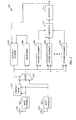
- FIG. 5 depicts a block diagram of a multi-carrier transmitter system 500 in accordance with various aspects of the invention.
- the multi-carrier transmitter system 500 is shown for a multi-carrler system composing of three carriers. Fewer or higher number of carriers may be used.
- the blocks 300A, 300B and 300C may operating in accordance with various operating aspects of block 300 shown in FIG. 3 to produce signals 399A, 399B and 399C.
- the signals 399A-C are modulated and carry the channel data for each respective carrier signal.
- Each signal passes through a pulse shaping filter, such as filters 501A, 501B and 501C for respectively modulated signals 399A, 399B and 399C.
- the resulting signals are combined in a combiner 502/ However, before combining, the signals are either passed through or up-converted to create a combined signal 503 that may pass through a single process of up-conversion at the carrier frequency "fc" at up-converter 513.
- the resulting signal 504 may have the frequency spectrum as represented by the curves 460, 461 and 462.
- one of the signals at the output of filters 501A, 501 B and 501C may pass through directly without any up-conversion.
- the other two signals are passed through frequency up-conversion in blocks 511B and 511C.
- two out of three signals before combining in combiner 502 are delayed.
- the amount of delay is selected based on the number of carriers in the multi-carrier signal 504. For example, if three carriers are in the multi-carrier signal 504, the amount of delay in a delay block 512B may be set approximately equal to an amount of time as represented by one third of a chip time used in the system. A chip time is equal to the inverse of the PN sequence frequency used in the spreading process of blocks 300A, 300B and 300C. For example, PN sequence of the 1.2288 Mcps may be used. Accordingly, the amount of delay in a delay block 512C may be set approximately equal to an amount of time as represented by two third of a chip time used in the system. As such, the signals at the combiner 502 are delayed from each other.
- the resulting multi-carrier signal 504 has a reduced PAR, in accordance with various aspects of the invention.
- An amplifier 520 may be maintained to operate within its linear operating range.
- the signals represented may be in complex form represented by in-phase and quadrature signals.
- the delay of the signal being delayed may be set equal to one half of a chip time. Therefore, as a generalization, the amount of delay is equal to "one chip tlme/N", where N is equal to the number of carriers In the multi-carrier signal, Such a generalization operates to produce a multi-carrier signal at a reduced PAR.
- the filters 501A, 501B and 501C do not have a symmetrical pulse shape, the amount of delay may not be equally spaced in time within a chip time or a symbol time. The spacing of the delay times over one chip time or a symbol time would be skewed in accordance with the asymmetrical nature of the pulse shape of the filters.
- An antenna 521 may be used for transmission of the amplified signal to a destination.
- the signal may be the forward link signal transmitted to a number of mobile stations in communication system 100.
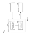
- the transmitter system 600 may be combined with receiver 200 in a transceiver system 400 shown In FIG. 6 for operation in a base station.
- a processor 401 may be coupled to receiver 200 and transmitter 500 to process the received and transmitted data.
- Various aspects of the receiver 200 and transmitter 500 may be common, even though receiver 200 and transmitter 500 are shown separately.
- receiver 200 and transmitter 500 may share a common local oscillator and a common antenna system for RF/IF receiving and transmitting.
- transmit data processing block 403 prepares the data for transmission on various transmit channels.
- Transmitter 500 receives the data for transmission on input 405, and transmits the data from an antenna system.
- the decoded data are received at processor 400 at an input 404.
- Received data are processed In received data processing block 402 in processor 401.
- Various operations of processor 401 may be integrated in a single or multiple processing units.
- the transceiver 400 may be connected to another device.
- the transceiver 400 may be an integral part of the device.
- the device may be a computer or may operate similar to a computer.
- the device may be connected to a data network, such as Internet.
- the base station through several connections may be connected to a network, such as Internet.
- processor 401 may control the amount of delay in delay blocks 512B and 512C based on the number of carriers in the multi-carrier signal 504.
- a flow chart 700 is depicted for determining the delay time of the delay blocks 512B and 512C.
- the processor 401 may determine the number of carriers in the multi-carrier signal 504.
- the processor 401 may determine the chip time of the PN sequence being used in block 300.
- the processor 401 may determine the delay time of each carrier in the multi-carrier signal based on the determined chip time and the number of carriers in the multi-carrier signal 504. One of the carriers is not delayed at all.
- the delay for other carriers is 1/3 and 2/3 of a chip time for a multi-carrier signal composed of three carriers, for example.
- the transmitter system 500 may be a digital transmitter system.
- the digital samples of the signals may need to go through a process of decimation or interpolation to have proper number of samples for the delay process.
- the delaying process may be based on a number of signal samples. For example, if the signals are produced at the sampling frequency of two samples per chip, the samples are interpolated by a factor of three and decimated by a factor of two to produce signals at three samples per chip. In this case, one of the carriers is delayed by one sample and the other by two samples to produce delayed signals.
- the delayed signals are, therefore, delayed by 1/3 chip time and 2/3 chip time respectively,
- the delay of each signal may be based on the number of carriers in the multi-carrier signal and the data symbol duration. For example, in case of a three carrier multi-carrier signal, the delay is set at 1/3 and 2/3 of a symbol time.
- DSP digital signal processor
- ASIC application specific integrated circuit
- FPGA field programmable gate array
- a general purpose processor may be a microprocessor, but in the alternative, the processor may be any conventional processor, controller, micro controller, or state machine.
- a processor may also be implemented as a combination of computing devices, e.g., a combination of a DSP and a microprocessor, a plurality of microprocessors, one or more microprocessors In conjunction with a DSP core, or any other such configuration.
- a software module may reside in RAM memory, flash memory, ROM memory, EPHOM memory, EEPROM memory, registers, hard disk, a removable disk, a CD-ROM, or any other form of storage medium known in the art.
- An exemplary storage medium is coupled to the processor such that the processor can read information from, and write information to, the storage medium,
- the storage medium may be integral to the processor.
- the processor and the storage medium may reside in an ASIC.
- the ASIC may reside in a user terminal.
- the processor and the storage medium may reside as discrete components in a user terminal.
- an apparatus for producing a multi-carrier signal at a reduced peak to average power ratio comprising a control system for determining a number of carriers in said multi-carrier signal, determining chip time of a spreading sequence used for spreading said number of carriers and determining delay time for each of said number of carriers based on said determined number of carriers and said determined chip time; means for delaying said number of carriers by said determined delay time; a combiner for combining the delayed carriers to produce a reduced peak to average power ratio multi-carrier signal.
- the apparatus may further comprising a transmitter for transmitting said reduced peak to average power ratio multi-carrier signal.
- said transmitter may include a power amplifier for amplifying said reduced peak to average power ratio multi-carrier signal before transmission.
- a method for producing a multi-carrier signal at a reduced peak to average power ratio comprises determining a number of carriers in said multi-carrier signals, determining chip time of a spreading sequence used for spreading said number of carriers and determining delay time for each of said number of carriers based on said number of chip time and said determined number of carriers; delaying said number of carriers by said determined number of delay time; combining the delayed carriers to produce a reduced peak to average power ratio multi-carrier signal.
- the method may further comprising transmitting said reduced peak to average power ratio multi-carrier signal.
- said transmitting may include amplifying said reduced peak to average power ratio multi-carrier signal before said transmitting.
- an apparatus for producing a multi-carrier signal at a reduced peak to average power ratio comprises a plurality of modulators for modulating data for transmission over said multi-carrier signals, thereby, for producing a corresponding plurality of modulated carrier signals; means for delaying each of said plurality of modulated carrier signals by a determined delay time, wherein said delay time is based on a number of carriers in said plurality of modulated carrier signals and chip time of a spreading sequence used for spreading said plurality of modulated carrier signals; a combiner for combining the delayed plurality of modulated carrier signals to produce a reduced peak to average power ratio multi-carrier signal.
- the apparatus may further comprising a transmitter for transmitting said reduced peak to average power ratio multi-carrier signal.
- said transmitter may include a power amplifier for amplifying said reduced peak to average power ratio multi-earner signal before transmission.
- a method for producing a multi-carrier signal at a reduced peak to average power ratio comprises modulating data for transmission over said multi-carrier signal, thereby, producing a corresponding plurality of modulated carrier signals; delaying each of said plurality of modulated carrier signals by a determined delay time, wherein said delay time is based on a number of carriers in said plurality of modulated carrier signals and chip time of a spreading sequence used for spreading said plurality of modulated carrier signals; combining the delayed plurality of modulated carrier signals to produce a reduced peak to average power ratio multi-carrier signal.
- the method may further comprising transmitting said reduced peak to average power ratio multi-carrier signal.
- said transmitting may include amplifying said reduced peak to average power ratio multi-carrier signal before said transmitting.
- an apparatus for producing a multi-carrier signal at a reduced peak to average power ratio comprises a control system for determining a number of carriers in said multi-carrier signal, determining modulation symbol time of said number of carriers and determining delay time for each of said numbar of carriers based on said determined number of carriers and said determined symbol time; means for delaying said number of carriers by said determined delay time; a combiner for combining the delayed carriers to produce a reduced peak to average power ratio multi-carrier signal.
- the apparatus may further comprising a transmitter for transmitting said reduced peak to average power ratio multi-carrier signal.
- said transmitter may include a power amplifier for amplifying said reduced peak to average power ratio multi-carrier signal before transmission.
- a method for producing a multi-carrier signal at a reduced peak to average power ratio comprises determining a number of carriers in said multi-carrier signal, determining a modulation symbol time of said number of carriers and determining delay time for each of said number of carriers based on said number of symbol time and said determined number of carriers; delaying said number of carriers by said determined number of delay time; combining the delayed carriers to produce a reduced peak to average power ratio multi-carrier signal.
- the method may further comprising transmitting said reduced peak to average power ratio multi-carrier signal.
- said transmitting may include amplifying said reduced peak to average power ratio multi-carrier signal before said transmitting.
- an apparatus for producing a multi-carrier signal at a reduced peak to average power ratio comprises a plurality of modulators for modulating data for transmission over said multi-carrier signal, thereby, for producing a corresponding plurality of modulated carrier signals; means for delaying each of said plurality of modulated carrier signals by a determined delay time, wherein said delay time is based on a number of carriers in said plurality of modulated carrier signals and modulation symbol time of said plurality of modulated carrier signals; a combiner for combining the delayed plurality of modulated carrier signals to produce a reduced peak to average power ratio multi-carrier signal.
- the apparatus may further comprising a transmitter for transmitting said reduced peak to average power ratio multi-earner signal.
- said transmitter may include a power amplifier for amplifying said reduced peak to average power ratio multi-carrier signal before transmission.
- a method for producing a multi-carrier signal at a reduced peak to average power ratio comprises modulating data for transmission over said multi-carrier signal, thereby, producing a corresponding plurality of modulated carrier signals; delaying each of said plurality of modulated carrier signals by a determined delay time, wherein said delay time is based on a number of carriers in said plurality of modulated carrier signals and modulation symbol time of said plurality of modulated carrier signals; combining the delayed plurality of modulated carrier signals to produce a reduced peak to average power ratio multi-carrier signal.
- the method may further comprising transmitting said reduced peak to average power ratio multi-carrier signal.
- said transmitting includes amplifying said reduced peak to average power ratio multi-carrier signal before said transmitting.
Abstract
Description
- The present invention relates generally to the field of communication, and more specifically, to multi-carrler communications.
- The communication channels between a transmitter and a receiver may be transmitted over a bundle of several carriers, The carriers may be combined and amplified before transmission. The power amplifier used for amplification of the transmitted signal may have a limited linear operating range. Generally, operation of a power amplifier within its linear operating range reduces the undesired inter-modulation products that may be generated in the amplifier, In order to maintain the power amplifier within its linear operating range, the peak to average ratio (PAR) of the input signal is kept at a low level. One or more method and apparatus has been disclosed in the
U.S, patent number 6,044,103 , and6,310,869 , and theU.S. publication number 2001/0038065 , all incorporated by reference herein. In case of multi-carrier transmission, the PAR of the combined signal may not be controlled without substantial processing of each individual carrier signal and the combined signal. Therefore, there is a need for a method and apparatus for reducing the PAR of a combined signal in a multi-carrier transmission system. - Method and apparatus for reducing peak to average power ratio of a multi-carrier combined signal are disclosed, A control system determines a number of carriers in the multi-carrier signal, determines chip time of a spreading sequence used for spreading the number of carriers and determines a delay time for each of the number of carriers based on the determined number of carriers and the determined chip time. Delay blocks delay the number of carriers by the determined delay time. A combiner combines the delayed carriers to produce a reduced peak to average power ratio multi-carrier signal. A transmitter transmits the reduced peak to average power ratio multi-carrier signal. The transmitter may include an amplifier for amplifying the reduced peak to average power ratio multi-carrier signal before transmitting.
- The features, objects, and advantages of the present invention will become more apparent from the detailed description set forth below when taken in conjunction with the drawings in which like reference characters Identify correspondingly throughout and wherein:
-
FIG. 1 depicts a communication system capable of operating in accordance with various embodiments of the invention; -
FIG. 2 depicts a communication system receiver for receiving and decoding received data; -
FIG. 3 depicts a communication system transmitter for transmitting data; -
FIG. 4 depicts an exemplary frequency spectrum of a single carrier signal and multi-carrier signal; -
FIG. 5 depicts a transmitter system in accordance with various aspects of the invention; -
FIG. 6 depicts a transceiver system capable of operating in accordance with various embodiments of the invention; and -
FIG. 7 illustrates various steps for determining delay time of each carrier in the multi-carrier signal in accordance with various aspects of the invention. - Various embodiments of the invention may be incorporated in a wireless communication system operating in accordance with the code division multiple access (CDMA) technique which has been disclosed and described in various standards published by the Telecommunication Industry Association (TIA) and other standards organizations. Such standards include the TIA/EIA-95 standard, TIA/EIA-IS-2000 standard, IMT-2000 standard, UMTS and WCDMA standard, all incorporated by reference herein, A system for communication of data is also detailed in the "TIA/EIA/IS-865 cdma2000 High Rate Packet Data Air Interface Specification," incorporated by reference herein. A copy of the standards may be obtained by accessing the world wide web at the address: http://www.3gpp2.org, or by writing to TIA, Standards and Technology Department, 2500 Wilson Boulevard, Arlington, VA 22201, United States of America. The standard generally identified as UMTS standard, Incorporated by reference herein, may be obtained by contacting 3GPP Support Office, 650 Route des Lucioles-Sophia Antipolis, Valbonne-France.
- Generally stated, various aspects of the invention allow producing a multi-carrier signal at a reduced peak to average power ratio (PAR). In accordance with at least one aspect of the invention, a delay element is used to delay each carrier of the multi-carrier signal by an amount of delay before combining the signals. The resulting signal has a reduced PAR. A power amplifier while allowing the power amplifier to remain in its linear operating region may amplify the resulting signal.
- One or more exemplary embodiments described herein are set forth In the context of a digital wireless communication system. While use within this context is advantageous, different embodiments of the invention may be incorporated in different environments or configurations. In addition, various embodiments of the invention may involve communication systems operating in accordance with the frequency division multiple access (FDMA) techniques. In a FDMA system, several carriers at different frequencies may be combined to form a multi-carrier signal. The multi-carrier signal may be used for communications. In general, the various systems described herein may be formed using software-controlled processors, integrated circuits, or discrete logic. The data, instructions, commands, information, signals, symbols, and chips that may be referenced throughout the application are advantageously represented by voltages, currents, electromagnetic waves, magnetic fields or particles, optical fields or particles, or a combination thereof. In addition, the blocks shown in each block diagram may represent hardware or method steps.
-
FIG. 1 illustrates a general block diagram of acommunication system 100 capable of operating in accordance with any of the code division multiple access (CDMA) communication system standards while incorporating various embodiments of the invention.Communication system 100 may be for communications of voice, data or both. Generally,communication system 100 includes abase station 101 that provides communication links between a number of mobile stations, such as mobile stations 102-104, and between the mobile stations 102-104 and a public switch telephone anddata network 105. The mobile stations inFIG. 1 may be referred to as data access terminals (AT) and the base station as data access network (AN) without departing from the main scope and various advantages of the invention.Base station 101 may include a number of components, such as a base station controller and a base transceiver system. For simplicity, such components are not shown.Base station 101 may be in communication with other base stations, forexample base station 160. Amobile switching center 199 may control various operating aspects of thecommunication system 100 and in relation to a back-haul 197 betweennetwork 105 andbase stations -
Base stations 101 communicates with each mobile station that is in its coverage area via a forward link signal transmitted frombase station 101. The forward link signals targeted for mobile stations 102-104 may be summed to form aforward link signal 106. Theforward link signal 106 may be a multi-carrier forward link signal. Each of the mobile stations 102-104 receivingforward link signal 106 decodes theforward link signal 106 to extract the information that is targeted for its user.Base station 160 may also communicate with the mobile stations that are in its coverage area via a forward link signal transmitted frombase station 160. Mobile stations 102-104 communicate withbase stations -
Base stations mobile station 102 may be in close proximity ofbase stations base stations base station 101 transmits onforward link signal 106, andbase station 160 on theforward link signal 161, On the reverse link,mobile station 102 transmits onreverse link signal 107 to be received by bothbase stations mobile station 102, one of thebase stations mobile station 102. On the reverse link, bothbase stations mobile station 102. - The
communication system 100 may also employ use of pilot channels for proper decoding of various channels. A pilot channel contains a series of predefined data. A receiver receives the pilot channel to determine various characteristics of the propagation channel. One of the characteristics may be a carrier to Interference ratio (Ec/lo) of the pilot channel. The pilot channel may be used to decode other received channels. The forward and reverse links may have pilot channels. On the forward link, a base station may transmit a pilot channel for all the mobile stations in its coverage area. On the reverse link, each mobile station may combine the reverse link channels with a pilot channel. -
FIG. 2 illustrates a block diagram of areceiver 200 used for processing and demodulating the received CDMA signal.Receiver 200 may be used for decoding the Information on the reverse and forward links signals. Received (Rx) samples may be stored inRAM 204. Receive samples are generated by a radio frequency/intermediate frequency (RF/IF)system 290 and anantenna system 292. The RF/IF system 290 andantenna system 292 may include one or more components for receiving multi-carrier signals and RF/IF processing of the received signals. For example, RF/IFsystem 290 may include the RF/IF systems 290A and 290B, each being considered a receiver chain. More than two receiver chains may also be used. Each element ofantenna system 292 receives a multi-carrier signal, and passes the received multi-carrier signal to a receiver chain In the RF/IF system 290. Each receiver chain may be tuned to a particular carrier frequency to process one or more of the carriers in the received multl-carrier signal. RF/IF system 290 may be any conventional RF/IF receiver. The RF/IF system 290 may be a "zero" intermediate frequency (ZIF) receiver. The received RF signals are filtered, down-converted and digitized to form RX samples at base band frequencies. The samples are supplied to a demultiplexer (demux) 202, The output ofdemux 202 is supplied to asearcher unit 206 andfinger elements 208. Acontrol system 210 is coupled thereto. Acombiner 212 couples adecoder 214 to fingerelements 208.Control system 210 may be a microprocessor controlled by software, and may be located on the same integrated circuit or on a separate integrated circuit. The decoding function indecoder 214 may be in accordance with a turbo decoder or any other suitable decoding algorithms. - During operation, received samples are supplied to
demux 202.Demux 202 supplies the samples tosearcher unit 206 andfinger elements 208.Control system 210 configuresfinger elements 208 to perform demodulation and despreading of the received signal at different time offsets based on search results fromsearcher unit 206. Despreading of the channels Is performed by multiplying the received samples with the complex conjugate of the PN sequence and assigned Walsh function at a single timing hypothesis and digitally filtering the resulting samples, often with an integrate and dump accumulator circuit (not shown). Such a technique is commonly known in the art. Thesearcher 206 may decode the pilot channel to determine the channel condition, such as determining Ec/Io. If the Ec/Io of the pilot channel of the transmitting source is above a threshold, thecontrol system 210 may decide to assignfinger elements 208 to process other received channels from the same source. In the mobile station, various lists of base stations with adequate pilot channel Ec/Io are kept. The lists may Include an active list of base stations, a candidate list of base stations, a neighboring list of base stations and a remaining list of base stations. The lists of the base stations may be organized in accordance with the received Ec/Io level. The base stations in the active list have the strongest received Ec/Io.Receiver 200 may be used in a receiver portion ofbase stations -
FIG. 3 illustrates a block diagram of a transmitchannel processing block 300 for producing asignal 399, which may include a combination of two or more channels. Thesignal 399 may be used for one of the carriers in the multi-carrier transmission on the forward link or reverse link. The channel data for transmission are input to amodulator 301 for modulation. The modulation may be according to any of the commonly known modulation techniques such as QAM, PSK or BPSK. The data is encoded at a data rate inmodulator 301. The data rate may be selected by a data rate andpower level selector 303. The data rate selection may be based on feedback information received from a receiving destination. The receiving destination may be a mobile station or a base station. The feedback information may include the maximum allowed data rate. The maximum allowed data rate may be determined in accordance with various commonly known algorithms. The maximum allowed data rate very often is based on the channel condition, among other considered factors. The data rate andpower level selector 303 accordingly selects the data rate Inmodulator 301. The output ofmodulator 301 passes through a signal spreading operation and amplified in ablock 302 for transmission. The data rate andpower level selector 303 also selects a power level for the amplification level of the transmitted signal in accordance with the feedback information. The combination of the selected data rate and the power level allows proper decoding of the transmitted data at the receiving destination. The transmit power level may be limited within a predefined range. A pilot signal is also generated in ablock 307. The pilot signal is amplified to an appropriate level inblock 307. The pilot signal power level may be in accordance with the channel condition at the receiving destination. The pilot signal is combined with the channel signal in acombiner 308. The resulting combinedsignal 399 may be used for transmission via a multi-carrier single. -
FIG. 4 illustrates frequency spectrum of a single carrier and multi-carrier signal, which are helpful in understanding various aspects of the invention. When signal 399 is up-converted at the carrier frequency "fc", the carrier spectrum may appear as thecurve 461. The bandwidth of the signal may be equal to 1.25 MHz, for example. If a three-carrier signal is used, three signals such assignal 399 are each up-converted to different frequencies to form a multi-carrier signal. The frequency of one of the multi-carrier signal may be at "fc", another at "fc-fo" and another at "fc+fo". As a result, thecurves -
FIG. 5 depicts a block diagram of amulti-carrier transmitter system 500 in accordance with various aspects of the invention. Themulti-carrier transmitter system 500 is shown for a multi-carrler system composing of three carriers. Fewer or higher number of carriers may be used. Theblocks block 300 shown inFIG. 3 to producesignals signals 399A-C are modulated and carry the channel data for each respective carrier signal. Each signal passes through a pulse shaping filter, such asfilters signals combiner 502/ However, before combining, the signals are either passed through or up-converted to create a combinedsignal 503 that may pass through a single process of up-conversion at the carrier frequency "fc" at up-converter 513. The resultingsignal 504 may have the frequency spectrum as represented by thecurves signal 504 with the corresponding frequency spectrum, one of the signals at the output offilters blocks combiner 502 are delayed. The amount of delay is selected based on the number of carriers in themulti-carrier signal 504. For example, if three carriers are in themulti-carrier signal 504, the amount of delay in adelay block 512B may be set approximately equal to an amount of time as represented by one third of a chip time used in the system. A chip time is equal to the inverse of the PN sequence frequency used in the spreading process ofblocks delay block 512C may be set approximately equal to an amount of time as represented by two third of a chip time used in the system. As such, the signals at thecombiner 502 are delayed from each other. The resultingmulti-carrier signal 504 has a reduced PAR, in accordance with various aspects of the invention. Anamplifier 520, therefore, may be maintained to operate within its linear operating range. One ordinary skilled in the art may appreciate that the signals represented may be in complex form represented by in-phase and quadrature signals. - In case, the multi-carrier signal is composed of two carriers, the delay of the signal being delayed may be set equal to one half of a chip time. Therefore, as a generalization, the amount of delay is equal to "one chip tlme/N", where N is equal to the number of carriers In the multi-carrier signal, Such a generalization operates to produce a multi-carrier signal at a reduced PAR. However, if the
filters antenna 521 may be used for transmission of the amplified signal to a destination. The signal may be the forward link signal transmitted to a number of mobile stations incommunication system 100. - The transmitter system 600 may be combined with
receiver 200 in atransceiver system 400 shown InFIG. 6 for operation in a base station. Aprocessor 401 may be coupled toreceiver 200 andtransmitter 500 to process the received and transmitted data. Various aspects of thereceiver 200 andtransmitter 500 may be common, even thoughreceiver 200 andtransmitter 500 are shown separately. In one aspect,receiver 200 andtransmitter 500 may share a common local oscillator and a common antenna system for RF/IF receiving and transmitting. - On the transmitting side, transmit
data processing block 403 prepares the data for transmission on various transmit channels.Transmitter 500 receives the data for transmission oninput 405, and transmits the data from an antenna system. On the receiving side, after the received data are decoded, the decoded data are received atprocessor 400 at aninput 404. Received data are processed In receiveddata processing block 402 inprocessor 401. Various operations ofprocessor 401 may be integrated in a single or multiple processing units. Thetransceiver 400 may be connected to another device. Thetransceiver 400 may be an integral part of the device. The device may be a computer or may operate similar to a computer. The device may be connected to a data network, such as Internet. In case of incorporating thetransceiver 400 in a base station, the base station through several connections may be connected to a network, such as Internet. In accordance with various aspects of the invention,processor 401 may control the amount of delay in delay blocks 512B and 512C based on the number of carriers in themulti-carrier signal 504. - Referring to
FIG. 7 , aflow chart 700 is depicted for determining the delay time of the delay blocks 512B and 512C. Atstep 701, theprocessor 401 may determine the number of carriers in themulti-carrier signal 504. Atstep 702, theprocessor 401 may determine the chip time of the PN sequence being used inblock 300. Atstep 703, theprocessor 401 may determine the delay time of each carrier in the multi-carrier signal based on the determined chip time and the number of carriers in themulti-carrier signal 504. One of the carriers is not delayed at all. The delay for other carriers is 1/3 and 2/3 of a chip time for a multi-carrier signal composed of three carriers, for example. Thetransmitter system 500 may be a digital transmitter system. In order to determine the delay time and delay the carrier signals indelay blocks 5128 and 512C, the digital samples of the signals may need to go through a process of decimation or interpolation to have proper number of samples for the delay process. The delaying process may be based on a number of signal samples. For example, if the signals are produced at the sampling frequency of two samples per chip, the samples are interpolated by a factor of three and decimated by a factor of two to produce signals at three samples per chip. In this case, one of the carriers is delayed by one sample and the other by two samples to produce delayed signals. The delayed signals are, therefore, delayed by 1/3 chip time and 2/3 chip time respectively, - In a system that utilizes the FDMA techniques, the delay of each signal may be based on the number of carriers in the multi-carrier signal and the data symbol duration. For example, in case of a three carrier multi-carrier signal, the delay is set at 1/3 and 2/3 of a symbol time.
- Those of skill in the art would further appreciate that the various illustrative logical blocks, modules, circuits, and algorithm steps described in connection with the embodiments disclosed herein may be implemented as electronic hardware, computer software, or combinations of both. To clearly illustrate this interchangeability of hardware and software, various illustrative components, blocks, modules, circuits, and steps have been described above generally in terms of their functionality. Whether such functionality is implemented as hardware or software depends upon the particular application and design constraints imposed on the overall system. Skilled artisans may implement the described functionality in varying ways for each particular application, but such implementation decisions should not be Interpreted as causing a departure from the scope of the present invention.
- The various illustrative logical blocks, modules, and circuits described in connection with the embodiments disclosed herein may be implemented or performed with a general purpose processor, a digital signal processor (DSP), an application specific integrated circuit (ASIC), a field programmable gate array (FPGA) or other programmable logic device, discrete gate or transistor logic, discrete hardware components, or any combination thereof designed to perform the functions described herein. A general purpose processor may be a microprocessor, but in the alternative, the processor may be any conventional processor, controller, micro controller, or state machine. A processor may also be implemented as a combination of computing devices, e.g., a combination of a DSP and a microprocessor, a plurality of microprocessors, one or more microprocessors In conjunction with a DSP core, or any other such configuration.
- The steps of a method or algorithm described in connection with the embodiments disclosed herein may be embodied directly in hardware, in a software module executed by a processor, or in a combination. A software module may reside in RAM memory, flash memory, ROM memory, EPHOM memory, EEPROM memory, registers, hard disk, a removable disk, a CD-ROM, or any other form of storage medium known in the art. An exemplary storage medium is coupled to the processor such that the processor can read information from, and write information to, the storage medium, In the alternative, the storage medium may be integral to the processor. The processor and the storage medium may reside in an ASIC. The ASIC may reside in a user terminal. In the alternative, the processor and the storage medium may reside as discrete components in a user terminal.
- The previous description of the preferred embodiments is provided to enable any person skilled in the art to make or use the present invention. The various modifications to these embodiments will be readily apparent to those skilled in the art, and the generic principles defined herein may be applied to other embodiments without the use of the inventive faculty. Thus, the present invention is not intended to be limited to the embodiments shown herein but is to be accorded the widest scope consistent with the principles and novel features disclosed herein.
- Further embodiments comprise, for example, an apparatus for producing a multi-carrier signal at a reduced peak to average power ratio, comprising a control system for determining a number of carriers in said multi-carrier signal, determining chip time of a spreading sequence used for spreading said number of carriers and determining delay time for each of said number of carriers based on said determined number of carriers and said determined chip time; means for delaying said number of carriers by said determined delay time; a combiner for combining the delayed carriers to produce a reduced peak to average power ratio multi-carrier signal. The apparatus may further comprising a transmitter for transmitting said reduced peak to average power ratio multi-carrier signal. In the apparatus, said transmitter may include a power amplifier for amplifying said reduced peak to average power ratio multi-carrier signal before transmission.
- In one embodiment a method for producing a multi-carrier signal at a reduced peak to average power ratio, comprises determining a number of carriers in said multi-carrier signals, determining chip time of a spreading sequence used for spreading said number of carriers and determining delay time for each of said number of carriers based on said number of chip time and said determined number of carriers; delaying said number of carriers by said determined number of delay time; combining the delayed carriers to produce a reduced peak to average power ratio multi-carrier signal. The method may further comprising transmitting said reduced peak to average power ratio multi-carrier signal. In the method, said transmitting may include amplifying said reduced peak to average power ratio multi-carrier signal before said transmitting.
- In one embodiment, an apparatus for producing a multi-carrier signal at a reduced peak to average power ratio, comprises a plurality of modulators for modulating data for transmission over said multi-carrier signals, thereby, for producing a corresponding plurality of modulated carrier signals; means for delaying each of said plurality of modulated carrier signals by a determined delay time, wherein said delay time is based on a number of carriers in said plurality of modulated carrier signals and chip time of a spreading sequence used for spreading said plurality of modulated carrier signals; a combiner for combining the delayed plurality of modulated carrier signals to produce a reduced peak to average power ratio multi-carrier signal. The apparatus may further comprising a transmitter for transmitting said reduced peak to average power ratio multi-carrier signal. In the apparatus, said transmitter may include a power amplifier for amplifying said reduced peak to average power ratio multi-earner signal before transmission.
- In one embodiment, a method for producing a multi-carrier signal at a reduced peak to average power ratio, comprises modulating data for transmission over said multi-carrier signal, thereby, producing a corresponding plurality of modulated carrier signals; delaying each of said plurality of modulated carrier signals by a determined delay time, wherein said delay time is based on a number of carriers in said plurality of modulated carrier signals and chip time of a spreading sequence used for spreading said plurality of modulated carrier signals; combining the delayed plurality of modulated carrier signals to produce a reduced peak to average power ratio multi-carrier signal. The method may further comprising transmitting said reduced peak to average power ratio multi-carrier signal. In the method, said transmitting may include amplifying said reduced peak to average power ratio multi-carrier signal before said transmitting.
- In one embodiment, an apparatus for producing a multi-carrier signal at a reduced peak to average power ratio, comprises a control system for determining a number of carriers in said multi-carrier signal, determining modulation symbol time of said number of carriers and determining delay time for each of said numbar of carriers based on said determined number of carriers and said determined symbol time; means for delaying said number of carriers by said determined delay time; a combiner for combining the delayed carriers to produce a reduced peak to average power ratio multi-carrier signal. The apparatus may further comprising a transmitter for transmitting said reduced peak to average power ratio multi-carrier signal. In the apparatus, said transmitter may include a power amplifier for amplifying said reduced peak to average power ratio multi-carrier signal before transmission.
- In one embodiment, a method for producing a multi-carrier signal at a reduced peak to average power ratio, comprises determining a number of carriers in said multi-carrier signal, determining a modulation symbol time of said number of carriers and determining delay time for each of said number of carriers based on said number of symbol time and said determined number of carriers; delaying said number of carriers by said determined number of delay time; combining the delayed carriers to produce a reduced peak to average power ratio multi-carrier signal. The method may further comprising transmitting said reduced peak to average power ratio multi-carrier signal. In the method, said transmitting may include amplifying said reduced peak to average power ratio multi-carrier signal before said transmitting.
- In one embodiment, an apparatus for producing a multi-carrier signal at a reduced peak to average power ratio, comprises a plurality of modulators for modulating data for transmission over said multi-carrier signal, thereby, for producing a corresponding plurality of modulated carrier signals; means for delaying each of said plurality of modulated carrier signals by a determined delay time, wherein said delay time is based on a number of carriers in said plurality of modulated carrier signals and modulation symbol time of said plurality of modulated carrier signals; a combiner for combining the delayed plurality of modulated carrier signals to produce a reduced peak to average power ratio multi-carrier signal. The apparatus may further comprising a transmitter for transmitting said reduced peak to average power ratio multi-earner signal. In the apparatus, said transmitter may include a power amplifier for amplifying said reduced peak to average power ratio multi-carrier signal before transmission.
- In one embodiment, a method for producing a multi-carrier signal at a reduced peak to average power ratio, comprises modulating data for transmission over said multi-carrier signal, thereby, producing a corresponding plurality of modulated carrier signals; delaying each of said plurality of modulated carrier signals by a determined delay time, wherein said delay time is based on a number of carriers in said plurality of modulated carrier signals and modulation symbol time of said plurality of modulated carrier signals; combining the delayed plurality of modulated carrier signals to produce a reduced peak to average power ratio multi-carrier signal. The method may further comprising transmitting said reduced peak to average power ratio multi-carrier signal. In the method, said transmitting includes amplifying said reduced peak to average power ratio multi-carrier signal before said transmitting.
Claims (15)
- An apparatus for producing a multi-carrier signal at a reduced peak to average power ratio, comprising:means for filtering a plurality of carriers;means for delaying at least one of said plurality of carriers;means for combining the delayed carriers to produce a reduced peak to average power ratio multi-carrier signal.
- The apparatus according to claim 1, wherein said means for delaying at least one of said plurality of carriers is based on a number of said plurality of carriers.
- The apparatus according to claim 1, wherein said means for delaying at least one of said plurality of carriers is based on a number of signal samples.
- The apparatus according to claim 1, wherein said means for delaying at least one of said plurality of carriers comprises delaying by an amount equal to a chip time divided by a number of said plurality of carriers.
- The apparatus according to claim 1, wherein said means for delaying comprises means for upconverting at least one of said plurality of carriers,
- The apparatus according to claim 1, wherein said means for filtering comprises means for symmetrical pulse shape filtering.
- The apparatus according to claim 1, further comprising:means for transmitting said reduced peak to average power ratio multi-carrier signal.
- The apparatus according to claim 5, wherein one of said plurality of carriers is not delayed.
- The apparatus according to claim 7, wherein said transmitting includes amplifying said reduced peak to average power ratio multi-carrier signal before said transmitting.
- The apparatus according to claim 8, further comprising:a means for determining a chip time of a spreading sequence used for spreading said plurality of carriers; anda second means for upconverting the reduced peak to average power ratio multi-carrier signal to a single carrier frequency, wherein at least one of the delayed plurality of carriers is combined with a single non-delayed carrier to produce said reduced peak to average power ratio multi-carrier signal.
- A method for producing a multi-carrier signal at a reduced peak to average power ratio, comprising:filtering a plurality of carriers;delaying at least one of said plurality of carriers;combining the delayed carriers to produce a reduced peak to average power ratio multi-carrier signal.
- The method according to claim 11, wherein said delaying at least one of said plurality of carriers is based on a number of signal samples.
- The method according to claim 11, wherein said delaying comprises upconverting at least one of said plurality of carriers, wherein each of the at least one of said plurality of carriers are up-converted to a different frequency.
- The method according to claim 11, wherein said means for filtering comprises means for symmetrical pulse shape filtering.
- The method according to claim 11, further comprising:amplifying said reduced peak to average power ratio multi-carrier signal before said transmitting;determining a chip time of a spreading sequence used for spreading said plurality of carriers, wherein the chip time is approximately equal to an inverse of a spreading sequence frequency; andupconverting the reduced peak to average power ratio multi-carrier signal to a single carrier frequency, wherein one of said plurality of carriers is not delayed and wherein at least one of the delayed plurality of carriers is combined with a single non-delayed carrier to produce said reduced peak to average power ratio multi-canier signal.
Applications Claiming Priority (2)
| Application Number | Priority Date | Filing Date | Title |
|---|---|---|---|
| US10/132,992 US7266156B2 (en) | 2002-04-26 | 2002-04-26 | Method and apparatus for reducing peak to average power ratio of a multi-carrier signal |
| EP03724246.8A EP1504579B1 (en) | 2002-04-26 | 2003-04-25 | Method and apparatus for reducing peak to average power ratio of a multi-carrier signal |
Related Parent Applications (3)
| Application Number | Title | Priority Date | Filing Date |
|---|---|---|---|
| EP03724246.8 Division | 2003-04-25 | ||
| EP03724246.8A Division-Into EP1504579B1 (en) | 2002-04-26 | 2003-04-25 | Method and apparatus for reducing peak to average power ratio of a multi-carrier signal |
| EP03724246.8A Division EP1504579B1 (en) | 2002-04-26 | 2003-04-25 | Method and apparatus for reducing peak to average power ratio of a multi-carrier signal |
Publications (2)
| Publication Number | Publication Date |
|---|---|
| EP2204960A1 true EP2204960A1 (en) | 2010-07-07 |
| EP2204960B1 EP2204960B1 (en) | 2016-09-14 |
Family
ID=29248889
Family Applications (2)
| Application Number | Title | Priority Date | Filing Date |
|---|---|---|---|
| EP03724246.8A Expired - Lifetime EP1504579B1 (en) | 2002-04-26 | 2003-04-25 | Method and apparatus for reducing peak to average power ratio of a multi-carrier signal |
| EP10161180.4A Expired - Lifetime EP2204960B1 (en) | 2002-04-26 | 2003-04-25 | Method and apparatus for reducing peak to average power ratio of a multi-carrier signal |
Family Applications Before (1)
| Application Number | Title | Priority Date | Filing Date |
|---|---|---|---|
| EP03724246.8A Expired - Lifetime EP1504579B1 (en) | 2002-04-26 | 2003-04-25 | Method and apparatus for reducing peak to average power ratio of a multi-carrier signal |
Country Status (9)
| Country | Link |
|---|---|
| US (1) | US7266156B2 (en) |
| EP (2) | EP1504579B1 (en) |
| JP (1) | JP4283215B2 (en) |
| KR (1) | KR100928168B1 (en) |
| CN (1) | CN1656764B (en) |
| AU (1) | AU2003235472A1 (en) |
| BR (1) | BRPI0309501B1 (en) |
| TW (1) | TWI315618B (en) |
| WO (1) | WO2003092235A1 (en) |
Families Citing this family (29)
| Publication number | Priority date | Publication date | Assignee | Title |
|---|---|---|---|---|
| CA2442946A1 (en) * | 2002-09-30 | 2004-03-30 | Vcom Inc. | Method and apparatus for reducing peak to average power ratio in qam multi-channel blocks |
| US20050111576A1 (en) * | 2003-11-24 | 2005-05-26 | Kiomars Anvari | Peak-to-average reduction technique for multi-carrier power amplifiers |
| DE102004029236B4 (en) * | 2004-06-17 | 2006-08-03 | Infineon Technologies Ag | Method and device for reducing the dynamic range of a radio signal |
| US8570007B2 (en) * | 2005-09-06 | 2013-10-29 | Analog Devices, Inc. | Phase doubling for switching power supply |
| CN1787413B (en) * | 2005-10-28 | 2010-08-11 | 东南大学 | Transmission tech. scheme for low peak equal ratio orthogonal frequency division multiplex |
| CN1972264B (en) * | 2005-11-23 | 2010-05-05 | 中兴通讯股份有限公司 | A method for reducing peak to average ratio of multicarrier |
| CN101998610B (en) * | 2009-08-08 | 2014-06-11 | 中兴通讯股份有限公司 | Method and device for reducing multi-carrier mutual interference |
| CN102065529B (en) * | 2009-11-12 | 2013-08-21 | 中兴通讯股份有限公司 | Method and system for reducing multi-carrier peak average ratio |
| WO2012049912A1 (en) * | 2010-10-14 | 2012-04-19 | 三菱電機株式会社 | Transmitter apparatus, receiver apparatus and relay apparatus |
| US8848813B2 (en) * | 2012-12-10 | 2014-09-30 | Texas Instruments Incorporated | OFDM PAR reduction by substituting original in-band subcarriers after clipping |
| US8687734B1 (en) * | 2013-01-03 | 2014-04-01 | Harris Corporation | Non-causal orthogonal frequency division multiplexing tapered peak suppression |
| US9602228B1 (en) | 2013-01-18 | 2017-03-21 | Gregory R. Warnes | Method and apparatus for transmission and reception of a signal over multiple frequencies with time offset encoding at each frequency |
| US9967123B1 (en) | 2017-02-07 | 2018-05-08 | Texas Instruments Incorporated | Peak-to-average power reduction using guard tone filtering |
| US11082279B2 (en) | 2018-09-27 | 2021-08-03 | At&T Intellectual Property I, L.P. | Facilitation of reduction of peak to average power ratio for 5G or other next generation network |
| US10659270B2 (en) | 2018-10-10 | 2020-05-19 | At&T Intellectual Property I, L.P. | Mapping reference signals in wireless communication systems to avoid repetition |
| US11418992B2 (en) | 2018-11-02 | 2022-08-16 | At&T Intellectual Property I, L.P. | Generation of demodulation reference signals in advanced networks |
| US10432272B1 (en) | 2018-11-05 | 2019-10-01 | XCOM Labs, Inc. | Variable multiple-input multiple-output downlink user equipment |
| US10812216B2 (en) | 2018-11-05 | 2020-10-20 | XCOM Labs, Inc. | Cooperative multiple-input multiple-output downlink scheduling |
| US10756860B2 (en) | 2018-11-05 | 2020-08-25 | XCOM Labs, Inc. | Distributed multiple-input multiple-output downlink configuration |
| US10659112B1 (en) | 2018-11-05 | 2020-05-19 | XCOM Labs, Inc. | User equipment assisted multiple-input multiple-output downlink configuration |
| US11290172B2 (en) | 2018-11-27 | 2022-03-29 | XCOM Labs, Inc. | Non-coherent cooperative multiple-input multiple-output communications |
| US11063645B2 (en) | 2018-12-18 | 2021-07-13 | XCOM Labs, Inc. | Methods of wirelessly communicating with a group of devices |
| US10756795B2 (en) | 2018-12-18 | 2020-08-25 | XCOM Labs, Inc. | User equipment with cellular link and peer-to-peer link |
| US11330649B2 (en) | 2019-01-25 | 2022-05-10 | XCOM Labs, Inc. | Methods and systems of multi-link peer-to-peer communications |
| US10756767B1 (en) | 2019-02-05 | 2020-08-25 | XCOM Labs, Inc. | User equipment for wirelessly communicating cellular signal with another user equipment |
| US10735057B1 (en) | 2019-04-29 | 2020-08-04 | XCOM Labs, Inc. | Uplink user equipment selection |
| US10686502B1 (en) | 2019-04-29 | 2020-06-16 | XCOM Labs, Inc. | Downlink user equipment selection |
| US11032112B2 (en) * | 2019-10-18 | 2021-06-08 | Motorola Solutions, Inc. | Multi-carrier crest factor reduction |
| US11411779B2 (en) | 2020-03-31 | 2022-08-09 | XCOM Labs, Inc. | Reference signal channel estimation |
Citations (8)
| Publication number | Priority date | Publication date | Assignee | Title |
|---|---|---|---|---|
| US5045799A (en) * | 1989-09-28 | 1991-09-03 | Rockwell International Corporation | Peak to average power ratio reduction in a power amplifier with multiple carrier input |
| EP0849905A2 (en) * | 1996-12-17 | 1998-06-24 | Nec Corporation | CDMA Multi-code transmitter |
| US5838732A (en) * | 1994-10-31 | 1998-11-17 | Airnet Communications Corp. | Reducing peak-to-average variance of a composite transmitted signal generated by a digital combiner via carrier phase offset |
| US6044103A (en) | 1997-06-17 | 2000-03-28 | Qualcomm Inc. | Reduced peak-to-average amplitude dual channel link |
| US6236864B1 (en) * | 1998-11-27 | 2001-05-22 | Nortel Networks Limited | CDMA transmit peak power reduction |
| US6310869B1 (en) | 1998-08-31 | 2001-10-30 | Qualcomm Incorporated | Method and apparatus for reducing amplitude variations and interference in communication signals, such as in wireless communication signals employing inserted pilot symbols |
| US20010038065A1 (en) | 2000-05-08 | 2001-11-08 | Hajime Kimura | Close contact type sensor |
| US6330289B1 (en) * | 1998-10-16 | 2001-12-11 | Nortel Networks Limited | System for improving base station amplifier performance |
Family Cites Families (5)
| Publication number | Priority date | Publication date | Assignee | Title |
|---|---|---|---|---|
| GB2309363B (en) * | 1996-01-17 | 2000-07-12 | Motorola Ltd | Multicarrier communication system and method for peak power control |
| KR100233836B1 (en) * | 1997-08-21 | 1999-12-01 | 정선종 | Modulation apparatus of mc dsss system |
| US6249539B1 (en) * | 1998-06-15 | 2001-06-19 | Qualcomm Incorporated | System and method for narrowing the range of frequency uncertainty of a doppler shifted signal |
| JP3329322B2 (en) * | 1999-12-07 | 2002-09-30 | 株式会社ワイ・アール・ピー移動通信基盤技術研究所 | Multi-carrier transmission equipment |
| KR20010069611A (en) * | 2001-04-20 | 2001-07-25 | 유흥균 | PAPR Reduction Method by Delay Circiuts in Multi-carrier Communication System |
-
2002
- 2002-04-26 US US10/132,992 patent/US7266156B2/en not_active Expired - Lifetime
-
2003
- 2003-04-25 TW TW092109710A patent/TWI315618B/en not_active IP Right Cessation
- 2003-04-25 KR KR1020047017230A patent/KR100928168B1/en active IP Right Grant
- 2003-04-25 BR BRPI0309501A patent/BRPI0309501B1/en not_active IP Right Cessation
- 2003-04-25 JP JP2004500462A patent/JP4283215B2/en not_active Expired - Fee Related
- 2003-04-25 WO PCT/US2003/012940 patent/WO2003092235A1/en active Application Filing
- 2003-04-25 EP EP03724246.8A patent/EP1504579B1/en not_active Expired - Lifetime
- 2003-04-25 EP EP10161180.4A patent/EP2204960B1/en not_active Expired - Lifetime
- 2003-04-25 AU AU2003235472A patent/AU2003235472A1/en not_active Abandoned
- 2003-04-25 CN CN038122103A patent/CN1656764B/en not_active Expired - Fee Related
Patent Citations (8)
| Publication number | Priority date | Publication date | Assignee | Title |
|---|---|---|---|---|
| US5045799A (en) * | 1989-09-28 | 1991-09-03 | Rockwell International Corporation | Peak to average power ratio reduction in a power amplifier with multiple carrier input |
| US5838732A (en) * | 1994-10-31 | 1998-11-17 | Airnet Communications Corp. | Reducing peak-to-average variance of a composite transmitted signal generated by a digital combiner via carrier phase offset |
| EP0849905A2 (en) * | 1996-12-17 | 1998-06-24 | Nec Corporation | CDMA Multi-code transmitter |
| US6044103A (en) | 1997-06-17 | 2000-03-28 | Qualcomm Inc. | Reduced peak-to-average amplitude dual channel link |
| US6310869B1 (en) | 1998-08-31 | 2001-10-30 | Qualcomm Incorporated | Method and apparatus for reducing amplitude variations and interference in communication signals, such as in wireless communication signals employing inserted pilot symbols |
| US6330289B1 (en) * | 1998-10-16 | 2001-12-11 | Nortel Networks Limited | System for improving base station amplifier performance |
| US6236864B1 (en) * | 1998-11-27 | 2001-05-22 | Nortel Networks Limited | CDMA transmit peak power reduction |
| US20010038065A1 (en) | 2000-05-08 | 2001-11-08 | Hajime Kimura | Close contact type sensor |
Non-Patent Citations (1)
| Title |
|---|
| OHKUBO N ET AL: "A peak to average power ratio reduction of multicarrier CDMA using selected mapping", 2002 IEEE 56TH VEHICULAR TECHNOLOGY CONFERENCE PROCEEDINGS (CAT. NO.02CH37359), 2002 IEEE 56TH VEHICULAR TECHNOLOGY CONFERENCE PROCEEDINGS, VANCOUVER, BC, CANADA, 24-28 SEPT. 2002, 24 September 2002 (2002-09-24), 2002, Piscataway, NJ, USA, IEEE, USA, pages 2086 - 2090 VOL.4, XP002248124, ISBN: 0-7803-7467-3 * |
Also Published As
| Publication number | Publication date |
|---|---|
| CN1656764A (en) | 2005-08-17 |
| EP1504579B1 (en) | 2016-08-24 |
| KR20040104637A (en) | 2004-12-10 |
| KR100928168B1 (en) | 2009-11-25 |
| JP2005524283A (en) | 2005-08-11 |
| TWI315618B (en) | 2009-10-01 |
| EP2204960B1 (en) | 2016-09-14 |
| CN1656764B (en) | 2011-01-19 |
| BRPI0309501B1 (en) | 2016-12-20 |
| TW200400705A (en) | 2004-01-01 |
| JP4283215B2 (en) | 2009-06-24 |
| AU2003235472A1 (en) | 2003-11-10 |
| US7266156B2 (en) | 2007-09-04 |
| BR0309501A (en) | 2005-04-05 |
| WO2003092235A1 (en) | 2003-11-06 |
| EP1504579A1 (en) | 2005-02-09 |
| US20030202611A1 (en) | 2003-10-30 |
Similar Documents
| Publication | Publication Date | Title |
|---|---|---|
| EP1504579B1 (en) | Method and apparatus for reducing peak to average power ratio of a multi-carrier signal | |
| US7245600B2 (en) | Method and apparatus for determining reverse link load level for reverse link data scheduling in a CDMA communication system | |
| AU2002351185B2 (en) | Method and apparatus for a reverse link supplemental channel scheduling | |
| US20020159425A1 (en) | Radio communication apparatus and radio communication method | |
| US7480270B2 (en) | Method and apparatus for a reverse link supplemental channel scheduling | |
| US6779147B2 (en) | Method and apparatus for efficient use of communication resources in a CDMA communication system | |
| US7167458B2 (en) | Method and apparatus for determining a number of times a message is transmitted on a paging channel to a mobile station | |
| KR100934882B1 (en) | Power control of downlink shared channel dsch | |
| US6785549B2 (en) | Method and apparatus for matching operating revisions of a mobile station and a base station in a wireless data communication system | |
| US20080037411A1 (en) | Variable filtering for radio evolution | |
| EP1433348A1 (en) | Handoff method and apparatus with dual pilots in a communication system | |
| WO2001018987A1 (en) | Wireless communications apparatus and methods using intelligent modulation code assignment | |
| US7505427B2 (en) | Apparatus and method for improving signal-to-noise ratio in a multi-carrier CDMA communication system | |
| EP2057743B1 (en) | Variable filtering for radio evolution |
Legal Events
| Date | Code | Title | Description |
|---|---|---|---|
| PUAI | Public reference made under article 153(3) epc to a published international application that has entered the european phase |
Free format text: ORIGINAL CODE: 0009012 |
|
| 17P | Request for examination filed |
Effective date: 20100427 |
|
| AC | Divisional application: reference to earlier application |
Ref document number: 1504579 Country of ref document: EP Kind code of ref document: P |
|
| AK | Designated contracting states |
Kind code of ref document: A1 Designated state(s): AT BE BG CH CY CZ DE DK EE ES FI FR GB GR HU IE IT LI LU MC NL PT RO SE SI SK TR |
|
| REG | Reference to a national code |
Ref country code: HK Ref legal event code: DE Ref document number: 1144857 Country of ref document: HK |
|
| GRAP | Despatch of communication of intention to grant a patent |
Free format text: ORIGINAL CODE: EPIDOSNIGR1 |
|
| INTG | Intention to grant announced |
Effective date: 20160422 |
|
| GRAS | Grant fee paid |
Free format text: ORIGINAL CODE: EPIDOSNIGR3 |
|
| GRAA | (expected) grant |
Free format text: ORIGINAL CODE: 0009210 |
|
| AC | Divisional application: reference to earlier application |
Ref document number: 1504579 Country of ref document: EP Kind code of ref document: P |
|
| AK | Designated contracting states |
Kind code of ref document: B1 Designated state(s): AT BE BG CH CY CZ DE DK EE ES FI FR GB GR HU IE IT LI LU MC NL PT RO SE SI SK TR |
|
| REG | Reference to a national code |
Ref country code: GB Ref legal event code: FG4D |
|
| REG | Reference to a national code |
Ref country code: CH Ref legal event code: EP |
|
| REG | Reference to a national code |
Ref country code: IE Ref legal event code: FG4D |
|
| REG | Reference to a national code |
Ref country code: AT Ref legal event code: REF Ref document number: 830065 Country of ref document: AT Kind code of ref document: T Effective date: 20161015 |
|
| REG | Reference to a national code |
Ref country code: DE Ref legal event code: R096 Ref document number: 60349402 Country of ref document: DE |
|
| REG | Reference to a national code |
Ref country code: HK Ref legal event code: WD Ref document number: 1144857 Country of ref document: HK |
|
| REG | Reference to a national code |
Ref country code: NL Ref legal event code: MP Effective date: 20160914 |
|
| PG25 | Lapsed in a contracting state [announced via postgrant information from national office to epo] |
Ref country code: FI Free format text: LAPSE BECAUSE OF FAILURE TO SUBMIT A TRANSLATION OF THE DESCRIPTION OR TO PAY THE FEE WITHIN THE PRESCRIBED TIME-LIMIT Effective date: 20160914 |
|
| REG | Reference to a national code |
Ref country code: AT Ref legal event code: MK05 Ref document number: 830065 Country of ref document: AT Kind code of ref document: T Effective date: 20160914 |
|
| PG25 | Lapsed in a contracting state [announced via postgrant information from national office to epo] |
Ref country code: GR Free format text: LAPSE BECAUSE OF FAILURE TO SUBMIT A TRANSLATION OF THE DESCRIPTION OR TO PAY THE FEE WITHIN THE PRESCRIBED TIME-LIMIT Effective date: 20161215 Ref country code: NL Free format text: LAPSE BECAUSE OF FAILURE TO SUBMIT A TRANSLATION OF THE DESCRIPTION OR TO PAY THE FEE WITHIN THE PRESCRIBED TIME-LIMIT Effective date: 20160914 Ref country code: SE Free format text: LAPSE BECAUSE OF FAILURE TO SUBMIT A TRANSLATION OF THE DESCRIPTION OR TO PAY THE FEE WITHIN THE PRESCRIBED TIME-LIMIT Effective date: 20160914 Ref country code: ES Free format text: LAPSE BECAUSE OF FAILURE TO SUBMIT A TRANSLATION OF THE DESCRIPTION OR TO PAY THE FEE WITHIN THE PRESCRIBED TIME-LIMIT Effective date: 20160914 |
|
| REG | Reference to a national code |
Ref country code: FR Ref legal event code: PLFP Year of fee payment: 15 |
|
| PG25 | Lapsed in a contracting state [announced via postgrant information from national office to epo] |
Ref country code: EE Free format text: LAPSE BECAUSE OF FAILURE TO SUBMIT A TRANSLATION OF THE DESCRIPTION OR TO PAY THE FEE WITHIN THE PRESCRIBED TIME-LIMIT Effective date: 20160914 Ref country code: RO Free format text: LAPSE BECAUSE OF FAILURE TO SUBMIT A TRANSLATION OF THE DESCRIPTION OR TO PAY THE FEE WITHIN THE PRESCRIBED TIME-LIMIT Effective date: 20160914 |
|
| PG25 | Lapsed in a contracting state [announced via postgrant information from national office to epo] |
Ref country code: CZ Free format text: LAPSE BECAUSE OF FAILURE TO SUBMIT A TRANSLATION OF THE DESCRIPTION OR TO PAY THE FEE WITHIN THE PRESCRIBED TIME-LIMIT Effective date: 20160914 Ref country code: SK Free format text: LAPSE BECAUSE OF FAILURE TO SUBMIT A TRANSLATION OF THE DESCRIPTION OR TO PAY THE FEE WITHIN THE PRESCRIBED TIME-LIMIT Effective date: 20160914 Ref country code: AT Free format text: LAPSE BECAUSE OF FAILURE TO SUBMIT A TRANSLATION OF THE DESCRIPTION OR TO PAY THE FEE WITHIN THE PRESCRIBED TIME-LIMIT Effective date: 20160914 Ref country code: BG Free format text: LAPSE BECAUSE OF FAILURE TO SUBMIT A TRANSLATION OF THE DESCRIPTION OR TO PAY THE FEE WITHIN THE PRESCRIBED TIME-LIMIT Effective date: 20161214 Ref country code: PT Free format text: LAPSE BECAUSE OF FAILURE TO SUBMIT A TRANSLATION OF THE DESCRIPTION OR TO PAY THE FEE WITHIN THE PRESCRIBED TIME-LIMIT Effective date: 20170116 Ref country code: BE Free format text: LAPSE BECAUSE OF FAILURE TO SUBMIT A TRANSLATION OF THE DESCRIPTION OR TO PAY THE FEE WITHIN THE PRESCRIBED TIME-LIMIT Effective date: 20160914 |
|
| REG | Reference to a national code |
Ref country code: DE Ref legal event code: R097 Ref document number: 60349402 Country of ref document: DE |
|
| PG25 | Lapsed in a contracting state [announced via postgrant information from national office to epo] |
Ref country code: IT Free format text: LAPSE BECAUSE OF FAILURE TO SUBMIT A TRANSLATION OF THE DESCRIPTION OR TO PAY THE FEE WITHIN THE PRESCRIBED TIME-LIMIT Effective date: 20160914 |
|
| PLBE | No opposition filed within time limit |
Free format text: ORIGINAL CODE: 0009261 |
|
| STAA | Information on the status of an ep patent application or granted ep patent |
Free format text: STATUS: NO OPPOSITION FILED WITHIN TIME LIMIT |
|
| PG25 | Lapsed in a contracting state [announced via postgrant information from national office to epo] |
Ref country code: DK Free format text: LAPSE BECAUSE OF FAILURE TO SUBMIT A TRANSLATION OF THE DESCRIPTION OR TO PAY THE FEE WITHIN THE PRESCRIBED TIME-LIMIT Effective date: 20160914 |
|
| 26N | No opposition filed |
Effective date: 20170615 |
|
| PG25 | Lapsed in a contracting state [announced via postgrant information from national office to epo] |
Ref country code: SI Free format text: LAPSE BECAUSE OF FAILURE TO SUBMIT A TRANSLATION OF THE DESCRIPTION OR TO PAY THE FEE WITHIN THE PRESCRIBED TIME-LIMIT Effective date: 20160914 |
|
| REG | Reference to a national code |
Ref country code: CH Ref legal event code: PL |
|
| REG | Reference to a national code |
Ref country code: IE Ref legal event code: MM4A |
|
| PG25 | Lapsed in a contracting state [announced via postgrant information from national office to epo] |
Ref country code: MC Free format text: LAPSE BECAUSE OF FAILURE TO SUBMIT A TRANSLATION OF THE DESCRIPTION OR TO PAY THE FEE WITHIN THE PRESCRIBED TIME-LIMIT Effective date: 20160914 |
|
| PG25 | Lapsed in a contracting state [announced via postgrant information from national office to epo] |
Ref country code: CH Free format text: LAPSE BECAUSE OF NON-PAYMENT OF DUE FEES Effective date: 20170430 Ref country code: LU Free format text: LAPSE BECAUSE OF NON-PAYMENT OF DUE FEES Effective date: 20170425 Ref country code: LI Free format text: LAPSE BECAUSE OF NON-PAYMENT OF DUE FEES Effective date: 20170430 |
|
| REG | Reference to a national code |
Ref country code: FR Ref legal event code: PLFP Year of fee payment: 16 |
|
| PG25 | Lapsed in a contracting state [announced via postgrant information from national office to epo] |
Ref country code: IE Free format text: LAPSE BECAUSE OF NON-PAYMENT OF DUE FEES Effective date: 20170425 |
|
| PGFP | Annual fee paid to national office [announced via postgrant information from national office to epo] |
Ref country code: FR Payment date: 20180320 Year of fee payment: 16 |
|
| PG25 | Lapsed in a contracting state [announced via postgrant information from national office to epo] |
Ref country code: HU Free format text: LAPSE BECAUSE OF FAILURE TO SUBMIT A TRANSLATION OF THE DESCRIPTION OR TO PAY THE FEE WITHIN THE PRESCRIBED TIME-LIMIT; INVALID AB INITIO Effective date: 20030425 |
|
| PG25 | Lapsed in a contracting state [announced via postgrant information from national office to epo] |
Ref country code: CY Free format text: LAPSE BECAUSE OF NON-PAYMENT OF DUE FEES Effective date: 20160914 |
|
| PG25 | Lapsed in a contracting state [announced via postgrant information from national office to epo] |
Ref country code: FR Free format text: LAPSE BECAUSE OF NON-PAYMENT OF DUE FEES Effective date: 20190430 |
|
| PG25 | Lapsed in a contracting state [announced via postgrant information from national office to epo] |
Ref country code: TR Free format text: LAPSE BECAUSE OF FAILURE TO SUBMIT A TRANSLATION OF THE DESCRIPTION OR TO PAY THE FEE WITHIN THE PRESCRIBED TIME-LIMIT Effective date: 20160914 |
|
| PGFP | Annual fee paid to national office [announced via postgrant information from national office to epo] |
Ref country code: GB Payment date: 20210331 Year of fee payment: 19 |
|
| PGFP | Annual fee paid to national office [announced via postgrant information from national office to epo] |
Ref country code: DE Payment date: 20210318 Year of fee payment: 19 |
|
| REG | Reference to a national code |
Ref country code: DE Ref legal event code: R119 Ref document number: 60349402 Country of ref document: DE |
|
| GBPC | Gb: european patent ceased through non-payment of renewal fee |
Effective date: 20220425 |
|
| PG25 | Lapsed in a contracting state [announced via postgrant information from national office to epo] |
Ref country code: GB Free format text: LAPSE BECAUSE OF NON-PAYMENT OF DUE FEES Effective date: 20220425 Ref country code: DE Free format text: LAPSE BECAUSE OF NON-PAYMENT OF DUE FEES Effective date: 20221103 |