EP2242180A1 - Resistance compensation method, circuit having a resistance compensation function, and circuit resistance test method - Google Patents
Resistance compensation method, circuit having a resistance compensation function, and circuit resistance test method Download PDFInfo
- Publication number
- EP2242180A1 EP2242180A1 EP10155087A EP10155087A EP2242180A1 EP 2242180 A1 EP2242180 A1 EP 2242180A1 EP 10155087 A EP10155087 A EP 10155087A EP 10155087 A EP10155087 A EP 10155087A EP 2242180 A1 EP2242180 A1 EP 2242180A1
- Authority
- EP
- European Patent Office
- Prior art keywords
- resistance
- semiconductor devices
- circuit
- predetermined
- variable resistor
- Prior art date
- Legal status (The legal status is an assumption and is not a legal conclusion. Google has not performed a legal analysis and makes no representation as to the accuracy of the status listed.)
- Granted
Links
Images


Classifications
-
- H—ELECTRICITY
- H04—ELECTRIC COMMUNICATION TECHNIQUE
- H04L—TRANSMISSION OF DIGITAL INFORMATION, e.g. TELEGRAPHIC COMMUNICATION
- H04L25/00—Baseband systems
- H04L25/02—Details ; arrangements for supplying electrical power along data transmission lines
- H04L25/0264—Arrangements for coupling to transmission lines
- H04L25/0298—Arrangement for terminating transmission lines
-
- G—PHYSICS
- G11—INFORMATION STORAGE
- G11C—STATIC STORES
- G11C2207/00—Indexing scheme relating to arrangements for writing information into, or reading information out from, a digital store
- G11C2207/22—Control and timing of internal memory operations
- G11C2207/2254—Calibration
-
- G—PHYSICS
- G11—INFORMATION STORAGE
- G11C—STATIC STORES
- G11C7/00—Arrangements for writing information into, or reading information out from, a digital store
- G11C7/10—Input/output [I/O] data interface arrangements, e.g. I/O data control circuits, I/O data buffers
- G11C7/1048—Data bus control circuits, e.g. precharging, presetting, equalising
-
- H—ELECTRICITY
- H03—ELECTRONIC CIRCUITRY
- H03K—PULSE TECHNIQUE
- H03K17/00—Electronic switching or gating, i.e. not by contact-making and –breaking
- H03K17/16—Modifications for eliminating interference voltages or currents
- H03K17/161—Modifications for eliminating interference voltages or currents in field-effect transistor switches
- H03K17/162—Modifications for eliminating interference voltages or currents in field-effect transistor switches without feedback from the output circuit to the control circuit
- H03K17/163—Soft switching
- H03K17/164—Soft switching using parallel switching arrangements
Definitions
- the present invention relates to a resistance compensation method, a circuit having a resistance compensation function, and a circuit resistance test method.
- the termination resistance of the interface part with a memory circuit is adjusted and controlled.
- the inclusion of a so-called ODT (On Die Termination) function is specified in order to adjust the termination resistance of the interface part between the memory circuit and the LSI circuit. Therefore, for instance, in the ODT circuit of the DDR2 memory interface, it is necessary to include a mechanism for adjusting the termination resistance to 75 ⁇ or 150 ⁇ in the LSI circuit.
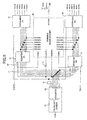
- FIG. 1 shows a diagram (a concept diagram) of a conventional analog termination resistor (ODT) circuit 1 and a termination resistor control circuit 6.
- Fig. 2 shows the details of the termination resistor control circuit 6.
- the value of a termination resistor 3 is determined by the control circuit 6 connected to a fixed resistor (a reference resistor) 5 serving as a reference.
- the configuration according to this method includes the termination resistor 3 composed of transistors, an input/output buffer 2, and the control circuit 6 for controlling the termination resistance.
- the termination resistor control circuit 6 is configured as shown in FIG. 2 .
- an operational amplifier receives a level in the current path of the series circuit of the reference resistor 5 and a transistor Tr.1, and generates the gate level of a transistor Tr.2.
- the control circuit 6 includes a transistor Tr.3 connected in series to the transistor Tr.2. The transistor Tr.3 is provided to obtain the same resistance as the reference resistor 5.
- Each of transistors Tr.4 and Tr.5 has a function as a switch.
- the transistors Tr.4 and Tr.5 are controlled by an ODTEN signal, and output respective level signals BIASP and BIASN that control the termination resistance.
- the level signals BIASP and BIASN are provided from the control circuit 6 to the gates of the corresponding transistors forming the termination resistor 3.
- the resistance of each of the transistors forming the termination resistor 3 is adjusted so as to be equal to the resistance of the reference resistor 5 by adjusting the gate level.
- the transistors (p-channel type and n-channel type FETs) forming the termination resistor 3, and semiconductor devices in the control circuit 6, such as the transistors Tr.1, Tr.2, Tr.3, etc., are all included in the same LSI circuit 1, and are manufactured in the same manufacturing process in the same chip. Accordingly, their characteristics may be substantially the same. Therefore, by realizing the same resistance as that of the reference resistor 5 by each of the transistors Tr.2 and Tr.3 in the control circuit 6, and by extracting the gate levels at that time directly as the level signals BIASP and BIASN and applying them to the gates of the transistors forming the termination resistor 3, the same resistance as the reference resistor 5 can be realized by each of the transistors forming the termination resistor 3.
- the signal levels of the level signals BIASP and BIASN are analog levels. That is, the resistances of the transistors forming the termination resistor 3 are controlled by controlling the physical state of the transistors with these levels. Accordingly, when interconnection lines for transmitting the level signals BIASP and BIASN are provided inside the LSI, the signals are sensitive to noise generated inside the chip. As a result, it is considered that when voltage applied to the gate terminal of each of the transistors forming the termination resistor 3 is slightly deviated, it is difficult to realize a desired resistance.
- the number of lines forming the interface between an LSI circuit and a memory circuit is generally large. Accordingly, if the control circuit 6 is provided common to the multiple lines, the level signals BIASP and BIASN are provided to each of the corresponding multiple termination resistors 3. As a result, the signals are sensitive to noise.
- control circuit 6 may be provided for each termination resistor 3, for instance. This makes it possible to increase noise immunity. However, this also causes a great increase in the number of terminals of the reference resistor 5 and in chip size, so that a desired specification of circuit size may not be satisfied.
- a more specific object of the present invention is to provide a method of controlling a termination resistor (for instance, the above-described ODT) that can significantly increase noise immunity without increasing the number of terminals of a reference resistor and chip size, a circuit having such a resistance compensation function, and a method of testing resistance in such a circuit.
- a termination resistor for instance, the above-described ODT
- a method for compensating for semiconductor device resistance including the step of (a) realizing a resistance equal to a desired resistance by one of combinations of a plurality of semiconductor devices, step (a) including the step of (b) sequentially selecting two or more of the semiconductor devices to be combined, and thereby sequentially changing a resistance realized by the selected two or more of the semiconductor devices to be combined.
- a circuit having a resistance compensation function including a resistance realization part configured to realize a resistance equal to a desired resistance by one of combinations of a plurality of semiconductor devices, wherein the resistance realization part performs an operation of sequentially selecting two or more of the semiconductor devices to be combined, and thereby sequentially changing a resistance realized by the selected two or more of the semiconductor devices to be combined.
- a computer-readable recording medium storing a program for causing a computer to control processing for compensating for semiconductor device resistance, the program comprising instructions for causing the computer to execute the step of (a) realizing a resistance equal to a desired resistance by one of combinations of a plurality of semiconductor devices, step (a) including the step of (b) sequentially selecting two or more of the semiconductor devices to be combined, and thereby sequentially changing a resistance realized by the selected two or more of the semiconductor devices to be combined.
- a method for testing a circuit including a resistance realization part configured to realize a resistance equal to a desired resistance by one of combinations of a plurality of semiconductor devices, the method including the step of verifying whether a resistance range realizable by the combinations of the semiconductor devices includes the desired resistance.
- a computer-readable recording medium storing a program for causing a computer to control testing of a circuit including a resistance realization part configured to realize a resistance equal to a desired resistance by one of combinations of a plurality of semiconductor devices, the program comprising instructions for causing the computer to execute the step of verifying whether a resistance range realizable by the combinations of the semiconductor devices includes the desired resistance.
- a realized resistance is determined by the selection of semiconductor devices or elements to be combined. Therefore, no analog elements are included in resistance realization. Accordingly, the resistance of a termination resistor can be adjusted with accuracy without being affected by noise. As a result, it is possible to ensure that the same resistance as a desired resistance can be realized as the resistance of the termination resistor, so that it is possible to realize high-speed, accurate data transfer between semiconductor devices or circuits with ease.
- a termination resistor adjustment circuit in order to adjust the resistance of the termination resistor.
- the termination resistor adjustment circuit includes a first variable resistor group set to be equal to the resistance of a predetermined reference resistor.
- the first variable resistor group is controlled digitally. That is, the resistance of the first variable resistor group is changed stepwise so as to generate the same resistance as the resistance of the reference resistor.
- the resistance of the termination resistor is adjusted so that an optimum value as the resistance of the termination resistor is obtained.
- the termination resistor adjustment circuit includes second and third variable resistor groups.
- the first and second variable resistor groups are configured to be capable of sharing the same information on resistance setting, and based on the information, the resistance of the second variable resistor group is set.
- the second variable resistor group whose resistance is thus set, is further employed as a reference resistor for adjusting (controlling) the third variable resistor group.
- the setting of the resistance of each of the first through third variable resistor groups is controlled by a counter. That is, the resistance of each of the first through third variable resistor groups is changed based on the counter value of the counter.
- the second and third variable resistor groups further have information on the setting of their resistances used as information for setting the resistance of the termination resistor. Accordingly, each of the second and third variable resistor groups has the function of transmitting the information to the termination resistor.
- a clock signal that drives the counter for setting the resistances of the first through third variable resistor groups has a frequency sufficiently lower than that of a reference operation clock signal applied inside the LSI.
- Information obtained by multiple resistance setting operations on the variable resistance groups is transmitted to the termination resistor as information for setting their resistance after being averaged in advance.
- a part configured to externally change the resistances of the first through third resistor groups is provided.
- the first variable resistor group is connected to a fixed resistor as the reference resistor, and a level detection circuit is connected to the center tap of the fixed resistor and the first variable resistor group so as to detect their resistances. Further, the first and second variable resistor groups are configured to share the same information as information for setting their resistances.
- the second variable resistor group is connected to the third variable resistor group.
- a level detection circuit is connected to the center tap of the second and third variable resistor groups so as to detect their resistances.
- a part configured to transmit the resistance setting information of the first and second variable resistance groups and the resistance setting information of the third variable resistance group to the outside is provided. By extracting the information, a verification test on the ranges in which the resistances of the first through third variable resistor groups are settable is conducted.
- a test is conducted to verify that the range in which the resistance of the first variable resistor group is settable includes the resistance of the fixed resistor.
- information on the thus obtained range including the resistance of the fixed resistor is transmitted to the second variable resistor group, and the resistance of the second variable resistor group is set over the range by the information.
- a test is conducted to verify that the settable resistance range of the third variable resistor group includes the resistance range of the second variable resistor group.
- the resistance of the third variable resistor group is settable over the resistance range obtained as that of the first variable resistor group including the resistance of the fixed resistor.
- the third variable resistor group is settable to the same resistance as that of the fixed resistor.
- a control method is digitalized so that information is transmitted with digital level signals ("H" or "L" level) of several bits. Further, by averaging the information, the frequency of updating the actual resistance of the termination resistor is controlled.
- test method is provided to ensure that the settable resistances of each of the first through third variable resistor groups include the resistance of the reference resistor in the LSI circuit as a product.
- FIG. 3 is a circuit diagram showing a portion of an LSI circuit 1000 as an embodiment of the present invention which portion relates to the interface with a memory circuit 2000.
- the LSI circuit 1000 includes an input/output buffer 100, an ODT circuit (a variable termination resistor part) 200 as a termination resistor, and an output buffer 500 for sending command information.
- the memory circuit 2000 which is accessed by the LSI circuit 1000 and is the counterpart device thereof in data transmission (input/output), includes an input/output buffer 700, an ODT circuit 600 as a termination resistor, and an input buffer 800 for receiving command information.
- a reference resistor 400 which provides a resistance serving as a reference for the resistance of the termination resistor realized in the ODT circuit 200, is connected to the LSI circuit 1000.
- the ODT circuit 200 includes a p-channel transistor 21p and an n-channel transistor 21n
- the counterpart ODT circuit 600 includes a p-channel transistor 61p and an n-channel transistor 61n.
- the transistors 21p and 21n are connected in series across a signal line DQ between a power supply line and a ground line so as to form a termination resistor.
- the transistors 61p and 61n are connected in series across the signal line DQ between a power supply line and a ground line so as to form a termination resistor.
- each termination resistor in the ODT circuit 200 By controlling the value of each termination resistor in the ODT circuit 200 appropriately so that the value is equal to the resistance of a reference resistor (for instance, the reference resistor 400), the signal level of the signal line DQ is appropriately controlled, so that high-speed, accurate data transfer can be realized.
- a reference resistor for instance, the reference resistor 400
- FIG. 4 is a circuit diagram showing a configuration of the ODT circuit 200 and a configuration of an ODT control circuit (a termination resistor control circuit) 300 included in the LSI circuit 1000.
- the ODT circuit 200 is configured by multiple parallel-connected pairs of p-channel type and n-channel type transistors 21p-0, 21n-0, 21p-1, 21n-1, ..., 21p-(N-1), 21n-(N-1), 21p-N, 21n-N, which form a termination resistor.
- Control signals PDRV[0], NDRV[0], PDRV[1], NDRV[1], ..., PDRV[N-1], NDRV[N-1], PDRV[N], NDRV[N] output from the ODT control circuit 300 are applied to the gates of the corresponding transistors, so that the transistors are turned ON/OFF.
- the substantial number of parallel-connected pairs of transistors connected across the signal line DQ between the power supply line and the ground line is adjusted, so that the resistance of the ODT circuit 200 as a termination resistor is controlled.
- the ODT control circuit 300 includes a variable resistor part 30, a counter part 40, and a logic part 10.
- the variable resistor part 30 is connected to the external reference resistor 400, and realizes a resistance.
- the counter part 40 and the logic part 10 control the variable resistor part 30.
- FIG. 5 is a circuit diagram showing the details of the configuration of the ODT control circuit 300.
- the circuit 300 includes a counter 42, a frequency divider 41 generating a clock input to the counter 42, logic circuits 11, 12, 13, 14, 15, 16, 17, and 18, and the variable resistor part 30.
- the logic part 10 shown in FIG. 4 includes a register (P) 12, a register (N) 11, an averaging circuit (P) 13, and an averaging circuit (N) 14. Signals TEST1 and TFST2 for inputting resistance setting information directly from outside are provided to the register (N) 11 and the register (P) 12, respectively.
- FIG. 6 is a circuit diagram showing the detailed configuration of the variable resistor part 30 shown in FIG. 4 and FIG. 5 .
- the circuit of the variable resistor part 30 includes first through third variable resistor circuit groups 30-1, 30-2, and 30-3, a first comparator circuit 35, and a second comparator circuit 34.
- the first variable resistor group 30-1 is configured by six n-channel type transistors 31n-0, 31n-1, ..., 31n-5 that are connected in parallel.
- the second variable resistor group 30-2 is configured by six n-channel type transistors 32n-0, 32n-1, ..., 32n-5 that are connected in parallel.
- the third variable resistor group 30-3 is configured by six p-channel type transistors 32p-0, 32p-1, ..., 32p-5 that are connected in parallel.
- each of the transistor groups forming the respective first through third variable resistor groups 30-1 through 30-3 corresponds to the transistor pairs forming the termination resistor.
- control signals NDRVNA0, NDRVNA1, ..., NDRVNA5 or control signals PDRVNA0, PDRVNA1, ..., PDRVNA5 are applied to the gates of the corresponding transistors of each of the variable resistor groups 30-1 through 30-3, so that the transistors are turned ON/OFF.
- a combination of transistors to be connected in parallel is determined. In consequence, a resistance realized by the parallel circuits is controlled.
- the second variable resistor group 30-2 is designed to have the same logic and the same physical shape as the first variable resistor group 30-1. Accordingly, the second variable resistor group 30-2 is configured to be able to obtain the same resistance as the first variable resistor group 30-1 when the same control signals NDRVNA0, NDRVNA1, ..., NDRVNA5 for the first variable resistor group 30-1 are applied to the second variable resistor group 30-2.
- the variable resistor group 30-3 is connected in series to the second variable resistor group 30-2, and is configured to realize an optimum resistance by turning ON/OFF the transistors 32p-0, 32p-1, ..., 32p-5 with the control signals PDRVNA0, PDRVNA1, ..., PDRVNA5 using the resistance of the second variable resistor group 30-2 as a reference.
- the above-mentioned control is described in detail below.
- the first and second resistor groups 30-1 and 30-2 are configured by n-channel transistors, and the third variable resistor group 30-3 is configured by p-channel transistors.
- the first variable resistor group 30-1 is connected to an external terminal (ODTVREF) 36 to which the reference resistor 400 is connected, and further is connected to the first comparator circuit 35 at the same connection.
- the first comparator circuit 35 compares a voltage level at the connection of the reference resistor 400, connected between the first comparator circuit 35 and a power supply line, and the first variable resistor group 30-1, connected between the first comparator circuit 35 and a ground line, and a predetermined threshold level VDDQ/2, thereby performing level detection at the connection.
- the second comparator circuit 34 is connected to the connection of the second and third resistor groups 30-2 and 30-3, and performs level detection at the connection of the third variable resistor group 30-3, connected between the second comparator circuit 34 and power supply level, and the second variable resistor group 30-2, connected between the second comparator circuit 34 and ground level.
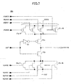
- FIG. 7 is a circuit diagram showing a detailed circuit configuration of the ODT circuit 200 shown in FIG. 4 .
- this circuit 200 is a variable termination resistor circuit where transistors 21p-0, 21p-1, 21p-2, ..., 21p-N are connected in parallel and transistors 21n-0, 21n-1, 21n-2, ..., 21n-N are connected in parallel.
- Control signals PDRV0, PDRV1, ..., PDRVN or control signals NDRV0, NDRV1, ..., NDRVN are applied to the gates of the corresponding transistors, so that the transistors are turned ON/OFF. As a result, the combination of transistors substantially connected in parallel is controlled, so that a resistance realized by the parallel circuit is controlled.
- FIG. 8 is a timing chart for illustrating a resistance setting operation by the ODT circuit 200.
- Waveforms shown in FIG. 8 are the output waveforms of the 0 th bit of the counter 42, the register (P) 12, and the register (N) 11.
- the resistances of the variable resistor groups 30-1 through 30-3 can be changed by inputting the counter value of the counter 42 thereto as control signals. Specifically, by controlling the combination of transistors substantially forming a parallel circuit as each variable resistor group, the resistance of the parallel circuit can be changed as described above.
- the horizontal axis represents time (cycle), and the vertical axis represents stepwise changes in the output values of each of the register (N) 11 and the register (P) 12.
- Changes in the output values of the registers 11 and 12 indicate resistances realized by the variable resistor groups 30-1 through 30-3 to which the output signals of the registers 11 and 12 are provided as control signals. That is, in FIG. 8 , with the output cycle of the 0 th bit of the counter 42 being one cycle, the values of the registers 11 and 12 are changed sequentially every cycle.
- the setting of the n-channel type transistor side that is, the variable resistor groups 30-1 and 30-2
- the setting of the p-channel type transistor side that is, the variable resistor group 30-3
- the corresponding one of the first and second comparator circuits 34 and 35 performs level detection. That is, the resistances of the reference resistor 400 and the first variable resistor group 30-1 are compared, and the resistances of the second and third variable resistor groups 30-2 and 30-3 are compared.
- a set value that is, an H/L (HIGH LEVEL/LOW LEVEL) combination of control signals, at the time when the resistances match each other is obtained as a result of the comparison.
- the set values thus obtained are averaged in the corresponding averaging circuit 13 or 14 so as to be transmitted to the ODT circuit 200 as resistance setting control information.
- the n-channel type transistor side (the first and second variable resistor groups 30-1 and 30-2) is set. That is, the n-bit (for instance, 7-bit in the case of FIG. 5 ) counter 42 is put into operation so as to change the resistance of each of the variable resistor groups 30-1 and 30-2. That is, the transistors of each of the variable resistor groups 30-1 and 30-2, having the control signals applied to their respective gates, are turned ON/OFF based on the H/L levels of the corresponding control signals output from the counter 42, the control signals corresponding to the bits thereof. Of the transistors, those turned ON form a parallel circuit, while those turned OFF do not form the parallel circuit. As a result, the resistance of the parallel circuit is changed.
- the transistors of each of the first through third variable resistor groups 30-1 through 30-3 are configured so that the ratio of their respective resistances obtained when the transistors are turned ON is as described below.
- the resistance of the parallel circuit formed by the transistors turned ON by the 6-bit (0 th to 5 th bits) output of the counter 42 can be configured so as to sequentially increase or decrease stepwise with the updating of the count value of the counter 42 as the output of each of the registers 11 and 12 shown in FIG. 8 .
- the transistors forming the ODT circuit 200 are also configured so that their respective resistances obtained when the transistors are turned ON satisfy the following ratio. As a result, the same resistance can be realized by the common control signals.
- transition of the output of the first comparator circuit 35 shown in FIG. 6 occurs at some point.
- the register (N) 11 latches control information at the point when transition of the output data COMPN of the first comparator circuit 35 occurs.
- the point at which the output data COMPN of the first comparator circuit 35 switches coincides with the point at which the resistance of the first variable resistor group 30-1 is set to substantially the same resistance as the external resistor (the reference resistor 400), and therefore, also coincides with the point at which the resistance of the second variable resistor group 30-2 is set to substantially the same resistance as the reference resistor 400.
- the threshold voltage VDDQ/2 serving as a reference in the comparison by the first comparator circuit 35 is set to a voltage that is the half of supply voltage.
- the resistance of the reference resistor 400 and the resistance of the first variable resistor group 30-1 are equalized, their respective voltage drops are equalized.
- a voltage level at their connection becomes the half of the supply voltage so as to be equal to the reference threshold voltage. Accordingly, the transition of the output of the first comparator circuit 35 occurs at that point.
- the third variable resistor group 30-3 is set based on the switching of the level of the (N-1) th bit (the 6 th bit in the illustrated case) of the counter 42. That is, as shown in FIG. 5 , the 6 th -bit output is provided directly to the register (N) 11, and is provided to the register (P) 12 after being inverted through the inverter 17. The output of each of the registers 11 and 12 is switched ON/OFF based on the level of the 6 th -bit output.
- the resistance of the third variable resistor group 30-3 is also changed sequentially by the output information of the counter 42 through the register (P) 12 in this case.
- the state transition of the second comparator circuit 34 occurs at some point, that is, at the time when the resistance of the third variable resistor group 30-3 thus changed sequentially is equalized substantially with the resistance of the second variable resistor group 30-2.
- the register (P) 12 detects this point by the output signal COMPP of the second comparator circuit 34, and latches the control information of this case (that is, the output bit information of the counter 42, or the control signals to the third variable resistor group 30-3).
- the resistance of the second variable resistor group 30-2 has been equalized substantially with the resistance of the external reference resistor 400 by the settings of the n-channel type transistor side (the first and second variable resistor groups 30-1 and 30-2). Accordingly, the resistance of the third variable resistor group 30-3 thus set based on the resistance of the second variable resistor group 30-2 is also substantially equal to the resistance of the external reference resistor 400.
- the register (N) 11 latches every control information item that equalizes the resistance of each of the first and second variable resistor groups 30-1 and 30-2 with that of the external reference resistor 400
- the register (P) 12 latches every control information item that equalizes the resistance of the third variable resistor group 30-3 with that of the external reference resistor 400.
- This resistance setting information is transmitted to and subjected to averaging in the corresponding averaging circuits (N) 13 and (P) 14, and is transmitted to the ODT circuit 200 as the resistance setting control information.
- the resistances of the first through third variable resistor groups 30-1 through 30-3 and the ODT circuit 200 which are formed by transistors, vary because of a process, temperature, and supply voltage. However, in actual operations, the resistance of the ODT circuit 200 does not vary so frequently. Accordingly, it is believed that there is little possibility of reducing substantial accuracy of resistance compensation even with a method that repeats the above-described n-channel type transistor side setting operation and p-channel type transistor side setting operation several times, thereafter averages the results in the averaging circuit (N) 13 and the averaging circuit (P) 14, and transmits the averaged control signals to the ODT circuit 200. Further, employment of this method eliminates the necessity of transmitting digital levels that are control signals for the resistance of the termination resistor every base clock cycle. This makes it possible to prevent an increase in current consumption.
- FIG. 9 is an operational flowchart of the above-described resistance setting operation.
- step S1 the counter of each of the averaging circuits 13 and 14 is reset to zero.
- step S2 the counter 42 is reset.
- step S3 the value of the counter 42 is set in the register (N) 11.
- the resistance of each of the first and second resistor groups 30-1 and 30-2 is set by the control signals corresponding to the counter values.
- step S4 the comparison result of the first comparator circuit 35 is determined. If the comparison result is NO TRANSITION, indicating the absence of transition (HIGH in step S4), in step S5, the counter 42 is incremented, and the operation returns to step S3.
- step S4 If the comparison result in step S4 is TRANSITION, indicating the presence of transition (LOW in step S4), that is, in the case where the resistance of the first variable resistor group 30-1 is substantially equal to the resistance of the reference resistor 400, the value of the register (N) 11 at this point (resistance setting information) is latched. Then, in step S6, the counter 42 is reset, and in step S7, the counter value of the counter 42 is set in the register (P) 12. As a result, the resistance of the third resistor group 30-3 is set by the control signals corresponding to the counter value. In step S8, the comparison result of the second comparator circuit 34 is determined. If the comparison result is NO TRANSITION, indicating the absence of transition (LOW in step S8), in step S9, the counter 42 is incremented, and the operation returns to step S7.
- TRANSITION indicating the presence of transition
- step S8 If the comparison result in step S8 is TRANSITION, indicating the presence of transition (HIGH in step S8), that is, in the case where the resistance of the third variable resistor group 30-3 is substantially equal to the resistance of the second variable resistor group 30-2, the value of the register (P) 12 at this point (resistance setting information) is latched. Then, in step S10, the counter value of each of the averaging circuits 13 and 14 is incremented by one, and in step S11, it is determined whether the counter value of each of the averaging circuits 13 and 14 reaches 256.
- step S12 the resistance setting information values that have been latched so far by the registers 11 and 12 are averaged by the averaging circuits 13 and 14, respectively, so as to be transmitted to the ODT circuit 200 as the resistance setting control information.
- step S13 the counter values of the averaging circuits 13 and 14 are reset to zero, and the operation returns to step S2. If the determination result of step S11 is NO, steps S2 through S11 described above are repeated.
- the termination resistance adjustment (compensation) method thus described with reference to FIG. 9 is built into an LSI as a control circuit.
- a method that externally operates the control is also possible.
- the external control method can be implemented by causing a computer to execute the method, using a program including instructions for causing the computer to execute the method.
- an interface for inputting data (such as resistance setting control signals) from the computer to a target LSI circuit and transmitting comparison results (the outputs of the first and second comparator circuits 35 and 34) from the LSI circuit to the computer is required.
- the program in this case is loaded into the computer via a portable recording medium such as a CD-ROM or a communications network such as the Internet.
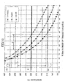
- FIG. 10 is a graph for illustrating the principles of a method for testing whether the settable resistances of each of the first through third variable resistor groups 30-1 through 30-3 of the ODT control circuit 300 of the LSI circuit 1000 can include the resistance of the reference resistor 400 according to a second embodiment of the present invention.
- the horizontal axis of this graph represents the number of transistor gates, and the vertical axis of this graph represents the resistance of a parallel circuit at the time when as many transistors as the corresponding number of transistor gates are turned ON to form the parallel circuit.
- an LSI circuit includes process variations. Accordingly, the characteristics of the transistors forming the LSI circuit cannot be determined uniquely, and vary within the range between SLOW (minimum transistor driveability) and FAST (maximum transistor driveability) shown in the graph of FIG. 10 .
- the resistance of the reference resistor 400 is 300 ⁇ , considering the above variations, the number of transistors forming a parallel circuit necessary to realize this resistance varies between 20 and 27 (Range A in FIG. 10 ). Taking these variations into account, when the number of transistors forming the parallel circuit is varied within the range of 20-27 with 300 ⁇ being targeted as the termination resistance, the resistance of the parallel circuit takes corresponding values within the range of 215-375 ⁇ (Range B in FIG. 10 ). This shows the range of values that can be taken by each of the first and second variable resistor groups 30-1 and 30-2 shown in FIG. 6 .
- the resistance of the first variable resistor group 30-1 is greater than the resistance of the reference resistor 400.
- the resistance of the first variable resistor group 30-1 is less than the resistance of the reference voltage 400.
- the second variable resistor group 30-2 has the same resistance as the first variable resistor group 30-1.
- the resistance of the second variable resistor group 30-2 is around 375 ⁇ (the upper limit of Range B) when the process characteristics are SLOW.
- the number of transistor gates for the third variable resistor group 30-3 is set to 16 so that the resistance of the third variable resistor group 30-3 is higher than that value (around 375 ⁇ ). In this state, it should be determined that the resistance of the third variable resistor group 30-3 is higher than the resistance of the second variable resistor group 30-2 (that is, Range C1 in FIG. 10 ).
- the actual number of transistors forming the parallel circuit of each of the first through third variable resistor groups 30-1 through 30-3 does not have to be 40 as specified above.
- substantially the same resistance as that by the above-described specified gate number/transistor number can be realized even when the number of transistors forming the parallel circuit is six as described above.
- FIG. 11A and FIG. 11B are operational flowcharts of a test for verifying that the transistors of each of the parallel circuits of the first through third variable resistor groups 30-1 through 30-3 can realize the resistance of the reference resistor 400.
- step S21 of FIG. 11A the number of transistor gates of the first variable resistor group 30-1 is set to 20, which corresponds to 20 parallel transistors. This setting is provided by changing the control signals NDRVNA0 through NDRVNA5 provided to the first variable resistor group 30-1 using the counter 42 and the register (N) 11 as described above.
- step S22 the resistance of the first variable resistor group 30-1 and the resistance of the reference resistor 400 are compared in the first comparator circuit 35. As a result, if it is determined in step S23 that the output of the first comparator circuit 35 is LOW level, that is, the resistance of the first variable resistor group 30-1 is lower, the LSI circuit is determined as out-of-spec.
- step S24 the number of transistor gates of the first variable resistor group 30-1 is set to 27, which corresponds to 27 parallel transistors. Then, the resistances are compared in the first comparator circuit 35 as described above. As a result, if it is determined in step S26 that the output of the first comparator circuit 35 is HIGH level, that is, the resistance of the first variable resistor group 30-1 is higher, the LSI circuit is determined as out-of-spec. On the other hand, if the output of the first comparator circuit 35 is LOW level, that is, the resistance of the first variable resistor group 30-1 is lower, the operation proceeds to step S27.
- step S27 the number of transistor gates of each of the first and second variable resistor groups 30-1 and 30-2 is set to 20, which corresponds to 20 parallel transistors.
- step S28 of FIG. 11B the number of transistor gates of the third variable resistor group 30-3 is set to 16, which corresponds to 16 parallel transistors.
- step S29 the resistances of the second and third variable resistor groups 30-2 and 30-3 are compared in the second comparator circuit 34. As a result, if it is determined in step S30 that the output of the second comparator circuit 34 is HIGH level, that is, the resistance of the third variable resistor group 30-3 is lower, the LSI circuit is determined as out-of-spec.
- step S31 the number of transistor gates of each of the first and second variable resistor groups 30-1 and 30-2 is set to 27, which corresponds to 27 parallel transistors.
- step S32 the number of transistor gates of the third variable resistor groups 30-3 is set to 40, which corresponds to 40 parallel transistors. Then, the resistances are compared in the second comparator circuit 34 as described above.
- step S34 if it is determined in step S34 that the output of the second comparator circuit 34 is LOW level, that is, the resistance of the third variable resistor group 30-3 is higher, the LSI circuit is determined as out-of-spec. On the other hand, if the output of the second comparator circuit 34 is HIGH level, that is, the resistance of the third variable resistor group 30-3 is lower, this operation ends. In this case, it is determined that the LSI circuit is standardized at least with respect to the resistances of the first through third variable resistor groups 30-1 through 30-3 in the ODT control circuit 300.
- the test method thus described with reference to FIG. 11 can be implemented by causing a computer to execute the method, using a program including instructions for causing the computer to execute the method.
- a program including instructions for causing the computer to execute the method.
- an interface for inputting test data (that is, resistance setting control signals) from the computer to an LSI circuit to be tested and transmitting comparison results (the outputs of the first and second comparator circuits 35 and 34) from the LSI circuit to the computer is required.
- the program in this case is loaded into the computer via a portable recording medium such as a CD-ROM or a communications network such as the Internet.
- the method thus digitizing a control method and including the process of averaging control signals may require more time before stabilization of resistance than the conventional analog method.
- the ODT circuit 200 and the ODT control circuit 300 are configured independent of each other as shown in FIG. 4 , so that it is possible to control resistance setting signals directly from outside. By thus externally providing resistance setting signals, it is possible to conduct the above-described test quickly without increasing test time.
- ODT circuit method of the present invention it is possible to realize a termination resistor (ODT) circuit significantly improved in noise immunity without increasing the number of reference resistor terminals and chip size. Further, it is also possible to prevent an increase in time required for testing an ODT control circuit for realizing the ODT circuit method.
- ODT termination resistor
- a realized resistance is determined by the selection of semiconductor devices or elements to be combined. Therefore, no analog elements are included in resistance realization. Accordingly, the resistance of a termination resistor can be adjusted or controlled with accuracy without being affected by noise. As a result, it is possible to ensure that the same resistance as a desired resistance can be realized as the resistance of the termination resistor, so that it is possible to realize high-speed, accurate data transfer between semiconductor devices or circuits easily.
Abstract
Description
- The present invention relates to a resistance compensation method, a circuit having a resistance compensation function, and a circuit resistance test method.
- In an LSI circuit required in design to perform high-speed data transfer, such as a so-called DDR2 (Double Data Rate 2) memory interface, the termination resistance of the interface part with a memory circuit is adjusted and controlled.
- In the case of the DDR2 memory interface, the inclusion of a so-called ODT (On Die Termination) function is specified in order to adjust the termination resistance of the interface part between the memory circuit and the LSI circuit. Therefore, for instance, in the ODT circuit of the DDR2 memory interface, it is necessary to include a mechanism for adjusting the termination resistance to 75 Ω or 150 Ω in the LSI circuit.
-
FIG. 1 shows a diagram (a concept diagram) of a conventional analog termination resistor (ODT)circuit 1 and a terminationresistor control circuit 6.Fig. 2 shows the details of the terminationresistor control circuit 6. - In this example, the value of a
termination resistor 3 is determined by thecontrol circuit 6 connected to a fixed resistor (a reference resistor) 5 serving as a reference. As shown inFIG. 1 , the configuration according to this method includes thetermination resistor 3 composed of transistors, an input/output buffer 2, and thecontrol circuit 6 for controlling the termination resistance. - The termination
resistor control circuit 6 is configured as shown inFIG. 2 . In a reference level generation part 6-1 of thecontrol circuit 6, an operational amplifier receives a level in the current path of the series circuit of thereference resistor 5 and a transistor Tr.1, and generates the gate level of a transistor Tr.2. Further, thecontrol circuit 6 includes a transistor Tr.3 connected in series to the transistor Tr.2. The transistor Tr.3 is provided to obtain the same resistance as thereference resistor 5. - Each of transistors Tr.4 and Tr.5 has a function as a switch. The transistors Tr.4 and Tr.5 are controlled by an ODTEN signal, and output respective level signals BIASP and BIASN that control the termination resistance. The level signals BIASP and BIASN are provided from the
control circuit 6 to the gates of the corresponding transistors forming thetermination resistor 3. The resistance of each of the transistors forming thetermination resistor 3 is adjusted so as to be equal to the resistance of thereference resistor 5 by adjusting the gate level. - That is, the transistors (p-channel type and n-channel type FETs) forming the
termination resistor 3, and semiconductor devices in thecontrol circuit 6, such as the transistors Tr.1, Tr.2, Tr.3, etc., are all included in thesame LSI circuit 1, and are manufactured in the same manufacturing process in the same chip. Accordingly, their characteristics may be substantially the same. Therefore, by realizing the same resistance as that of thereference resistor 5 by each of the transistors Tr.2 and Tr.3 in thecontrol circuit 6, and by extracting the gate levels at that time directly as the level signals BIASP and BIASN and applying them to the gates of the transistors forming thetermination resistor 3, the same resistance as thereference resistor 5 can be realized by each of the transistors forming thetermination resistor 3. - See Japanese Laid-Open Patent Applications No.
2002-199030 10-133792 - However, according to the configuration shown in
FIGS. 1 and2 , the signal levels of the level signals BIASP and BIASN are analog levels. That is, the resistances of the transistors forming thetermination resistor 3 are controlled by controlling the physical state of the transistors with these levels. Accordingly, when interconnection lines for transmitting the level signals BIASP and BIASN are provided inside the LSI, the signals are sensitive to noise generated inside the chip. As a result, it is considered that when voltage applied to the gate terminal of each of the transistors forming thetermination resistor 3 is slightly deviated, it is difficult to realize a desired resistance. - In particular, the number of lines forming the interface between an LSI circuit and a memory circuit is generally large. Accordingly, if the
control circuit 6 is provided common to the multiple lines, the level signals BIASP and BIASN are provided to each of the correspondingmultiple termination resistors 3. As a result, the signals are sensitive to noise. - In order to solve this problem, the
control circuit 6 may be provided for eachtermination resistor 3, for instance. This makes it possible to increase noise immunity. However, this also causes a great increase in the number of terminals of thereference resistor 5 and in chip size, so that a desired specification of circuit size may not be satisfied. - Accordingly, it is a general object of the present invention to provide a resistance compensation method and a circuit having a resistance compensation function in which the above-described disadvantages are eliminated.
- A more specific object of the present invention is to provide a method of controlling a termination resistor (for instance, the above-described ODT) that can significantly increase noise immunity without increasing the number of terminals of a reference resistor and chip size, a circuit having such a resistance compensation function, and a method of testing resistance in such a circuit.
- The above objects of the present invention are achieved by a method for compensating for semiconductor device resistance, including the step of (a) realizing a resistance equal to a desired resistance by one of combinations of a plurality of semiconductor devices, step (a) including the step of (b) sequentially selecting two or more of the semiconductor devices to be combined, and thereby sequentially changing a resistance realized by the selected two or more of the semiconductor devices to be combined.
- The above objects of the present invention are also achieved by a circuit having a resistance compensation function, including a resistance realization part configured to realize a resistance equal to a desired resistance by one of combinations of a plurality of semiconductor devices, wherein the resistance realization part performs an operation of sequentially selecting two or more of the semiconductor devices to be combined, and thereby sequentially changing a resistance realized by the selected two or more of the semiconductor devices to be combined.
- The above objects of the present invention are also achieved by a computer-readable recording medium storing a program for causing a computer to control processing for compensating for semiconductor device resistance, the program comprising instructions for causing the computer to execute the step of (a) realizing a resistance equal to a desired resistance by one of combinations of a plurality of semiconductor devices, step (a) including the step of (b) sequentially selecting two or more of the semiconductor devices to be combined, and thereby sequentially changing a resistance realized by the selected two or more of the semiconductor devices to be combined.
- The above objects of the present invention are also achieved by a method for testing a circuit including a resistance realization part configured to realize a resistance equal to a desired resistance by one of combinations of a plurality of semiconductor devices, the method including the step of verifying whether a resistance range realizable by the combinations of the semiconductor devices includes the desired resistance.
- The above objects of the present invention are also achieved by a computer-readable recording medium storing a program for causing a computer to control testing of a circuit including a resistance realization part configured to realize a resistance equal to a desired resistance by one of combinations of a plurality of semiconductor devices, the program comprising instructions for causing the computer to execute the step of verifying whether a resistance range realizable by the combinations of the semiconductor devices includes the desired resistance.
- According to the present invention, a realized resistance is determined by the selection of semiconductor devices or elements to be combined. Therefore, no analog elements are included in resistance realization. Accordingly, the resistance of a termination resistor can be adjusted with accuracy without being affected by noise. As a result, it is possible to ensure that the same resistance as a desired resistance can be realized as the resistance of the termination resistor, so that it is possible to realize high-speed, accurate data transfer between semiconductor devices or circuits with ease.
- Other objects, features and advantages of the present invention will become more apparent from the following detailed description when read in conjunction with the accompanying drawings, in which:
-
FIG. 1 is a circuit diagram showing part of an LSI configuration including a conventional ODT circuit; -
FIG. 2 is a circuit diagram showing an internal circuit of a control circuit shown inFIG. 1 ; -
FIG. 3 is a circuit diagram showing a partial configuration of an LSI circuit according to a first embodiment of the present invention; -
FIG. 4 is a circuit diagram showing further details of the partial configuration of the LSI circuit shown inFIG. 3 including an ODT control circuit implementing a resistance compensation method according to the first embodiment of the present invention; -
FIG. 5 is a circuit diagram showing an internal configuration of the ODT control circuit shown inFIG. 4 according to the first embodiment of the present invention; -
FIG. 6 is a circuit diagram showing an internal configuration of a variable resistor part shown inFIG. 5 according to the first embodiment of the present invention; -
FIG. 7 is a circuit diagram showing the details of the ODT circuit shown inFIG. 4 according to the first embodiment of the present invention; -
FIG. 8 is a timing chart for illustrating a resistance setting operation performed by a logic part of the ODT control circuit shown inFIGS. 4 and5 according to the first embodiment of the present invention; -
FIG. 9 is an operational flowchart of the resistance setting operation performed by the logic part of the ODT control circuit shown inFIGS. 4 and5 according to the first embodiment of the present invention; -
FIG. 10 is a graph for illustrating the principles of a resistance test method, showing variations in device resistance, according to a second embodiment of the present invention; and -
FIGS. 11A and11B are operational flowcharts of the resistance test method according to the second embodiment of the present invention. - A description is given below, with reference to the accompanying drawings, of preferred embodiments of the present invention.
- According to the embodiments of the present invention, in an LSI having a termination resistor in a chip, a termination resistor adjustment circuit is provided in order to adjust the resistance of the termination resistor. The termination resistor adjustment circuit includes a first variable resistor group set to be equal to the resistance of a predetermined reference resistor. The first variable resistor group is controlled digitally. That is, the resistance of the first variable resistor group is changed stepwise so as to generate the same resistance as the resistance of the reference resistor. Using the first variable resistor group, thus having the same resistance as that of the reference resistor, as a reference, the resistance of the termination resistor is adjusted so that an optimum value as the resistance of the termination resistor is obtained.
- Besides the first variable resistor group, the termination resistor adjustment circuit includes second and third variable resistor groups. Of these, the first and second variable resistor groups are configured to be capable of sharing the same information on resistance setting, and based on the information, the resistance of the second variable resistor group is set. The second variable resistor group, whose resistance is thus set, is further employed as a reference resistor for adjusting (controlling) the third variable resistor group.
- The setting of the resistance of each of the first through third variable resistor groups is controlled by a counter. That is, the resistance of each of the first through third variable resistor groups is changed based on the counter value of the counter.
- The second and third variable resistor groups further have information on the setting of their resistances used as information for setting the resistance of the termination resistor. Accordingly, each of the second and third variable resistor groups has the function of transmitting the information to the termination resistor.
- A clock signal that drives the counter for setting the resistances of the first through third variable resistor groups has a frequency sufficiently lower than that of a reference operation clock signal applied inside the LSI.
- Information obtained by multiple resistance setting operations on the variable resistance groups is transmitted to the termination resistor as information for setting their resistance after being averaged in advance.
- A part configured to externally change the resistances of the first through third resistor groups is provided. The first variable resistor group is connected to a fixed resistor as the reference resistor, and a level detection circuit is connected to the center tap of the fixed resistor and the first variable resistor group so as to detect their resistances. Further, the first and second variable resistor groups are configured to share the same information as information for setting their resistances. The second variable resistor group is connected to the third variable resistor group. A level detection circuit is connected to the center tap of the second and third variable resistor groups so as to detect their resistances. Further, a part configured to transmit the resistance setting information of the first and second variable resistance groups and the resistance setting information of the third variable resistance group to the outside is provided. By extracting the information, a verification test on the ranges in which the resistances of the first through third variable resistor groups are settable is conducted.
- That is, first, a test is conducted to verify that the range in which the resistance of the first variable resistor group is settable includes the resistance of the fixed resistor. Next, information on the thus obtained range including the resistance of the fixed resistor is transmitted to the second variable resistor group, and the resistance of the second variable resistor group is set over the range by the information. Then, using the thus set resistance range of the second variable resistor group as a reference, a test is conducted to verify that the settable resistance range of the third variable resistor group includes the resistance range of the second variable resistor group. Thus, in substance, it is verified that the resistance of the third variable resistor group is settable over the resistance range obtained as that of the first variable resistor group including the resistance of the fixed resistor. Thereby, it is also verified that the third variable resistor group is settable to the same resistance as that of the fixed resistor.
- Further, a part configured to externally change the resistances of the first through third resistor groups is provided.
- In order to realize such a configuration, in the preferred embodiments of the present invention, a control method is digitalized so that information is transmitted with digital level signals ("H" or "L" level) of several bits. Further, by averaging the information, the frequency of updating the actual resistance of the termination resistor is controlled.
- Further, a test method is provided to ensure that the settable resistances of each of the first through third variable resistor groups include the resistance of the reference resistor in the LSI circuit as a product.
- Further, in the case of digital control as described above, it may take more time before a resistance actually set with respect to the termination resistor is determined because of the averaging operation than in the case of the analog method. However, by providing a configuration that enables a desired value to be input externally as a digital level signal for controlling the termination resistor, it is possible to reduce time required for a product characteristic verification test.
- Next, an expatiation is given below of the embodiments of the present invention.
-
FIG. 3 is a circuit diagram showing a portion of anLSI circuit 1000 as an embodiment of the present invention which portion relates to the interface with amemory circuit 2000. Referring toFIG. 3 , theLSI circuit 1000 includes an input/output buffer 100, an ODT circuit (a variable termination resistor part) 200 as a termination resistor, and anoutput buffer 500 for sending command information. On the other hand, thememory circuit 2000, which is accessed by theLSI circuit 1000 and is the counterpart device thereof in data transmission (input/output), includes an input/output buffer 700, anODT circuit 600 as a termination resistor, and aninput buffer 800 for receiving command information. Areference resistor 400, which provides a resistance serving as a reference for the resistance of the termination resistor realized in theODT circuit 200, is connected to theLSI circuit 1000. - The
ODT circuit 200 includes a p-channel transistor 21p and an n-channel transistor 21n, and thecounterpart ODT circuit 600 includes a p-channel transistor 61p and an n-channel transistor 61n. Thetransistors transistors ODT circuit 200 appropriately so that the value is equal to the resistance of a reference resistor (for instance, the reference resistor 400), the signal level of the signal line DQ is appropriately controlled, so that high-speed, accurate data transfer can be realized. -
FIG. 4 is a circuit diagram showing a configuration of theODT circuit 200 and a configuration of an ODT control circuit (a termination resistor control circuit) 300 included in theLSI circuit 1000. As shown inFIG. 4 , theODT circuit 200 is configured by multiple parallel-connected pairs of p-channel type and n-channel type transistors 21p-0, 21n-0, 21p-1, 21n-1, ..., 21p-(N-1), 21n-(N-1), 21p-N, 21n-N, which form a termination resistor. Control signals PDRV[0], NDRV[0], PDRV[1], NDRV[1], ..., PDRV[N-1], NDRV[N-1], PDRV[N], NDRV[N] output from theODT control circuit 300 are applied to the gates of the corresponding transistors, so that the transistors are turned ON/OFF. Thus, in substance, the substantial number of parallel-connected pairs of transistors connected across the signal line DQ between the power supply line and the ground line is adjusted, so that the resistance of theODT circuit 200 as a termination resistor is controlled. - The
ODT control circuit 300 includes avariable resistor part 30, acounter part 40, and alogic part 10. Thevariable resistor part 30 is connected to theexternal reference resistor 400, and realizes a resistance. Thecounter part 40 and thelogic part 10 control thevariable resistor part 30. -
FIG. 5 is a circuit diagram showing the details of the configuration of theODT control circuit 300. - The
circuit 300 includes acounter 42, afrequency divider 41 generating a clock input to thecounter 42,logic circuits variable resistor part 30. Thelogic part 10 shown inFIG. 4 includes a register (P) 12, a register (N) 11, an averaging circuit (P) 13, and an averaging circuit (N) 14. Signals TEST1 and TFST2 for inputting resistance setting information directly from outside are provided to the register (N) 11 and the register (P) 12, respectively. -
FIG. 6 is a circuit diagram showing the detailed configuration of thevariable resistor part 30 shown inFIG. 4 andFIG. 5 . - The circuit of the
variable resistor part 30 includes first through third variable resistor circuit groups 30-1, 30-2, and 30-3, afirst comparator circuit 35, and asecond comparator circuit 34. The first variable resistor group 30-1 is configured by six n-channel type transistors 31n-0, 31n-1, ..., 31n-5 that are connected in parallel. The second variable resistor group 30-2 is configured by six n-channel type transistors 32n-0, 32n-1, ..., 32n-5 that are connected in parallel. The third variable resistor group 30-3 is configured by six p-channel type transistors 32p-0, 32p-1, ..., 32p-5 that are connected in parallel. - This case corresponds to the case where the pairs of the p-channel type and n-
channel type transistors 21p-0, 21n-0, 21p-1, 21n-1, ..., 21p-(N-1), 21n-(N-1), 21p-N, 21n-N forming the termination resistor inFIG. 4 are six in number (N = 5). That is, each of the transistor groups forming the respective first through third variable resistor groups 30-1 through 30-3 corresponds to the transistor pairs forming the termination resistor. - As shown in
FIG. 6 , control signals NDRVNA0, NDRVNA1, ..., NDRVNA5 or control signals PDRVNA0, PDRVNA1, ..., PDRVNA5 are applied to the gates of the corresponding transistors of each of the variable resistor groups 30-1 through 30-3, so that the transistors are turned ON/OFF. As a result, in substance, a combination of transistors to be connected in parallel is determined. In consequence, a resistance realized by the parallel circuits is controlled. - The second variable resistor group 30-2 is designed to have the same logic and the same physical shape as the first variable resistor group 30-1. Accordingly, the second variable resistor group 30-2 is configured to be able to obtain the same resistance as the first variable resistor group 30-1 when the same control signals NDRVNA0, NDRVNA1, ..., NDRVNA5 for the first variable resistor group 30-1 are applied to the second variable resistor group 30-2. The variable resistor group 30-3 is connected in series to the second variable resistor group 30-2, and is configured to realize an optimum resistance by turning ON/OFF the
transistors 32p-0, 32p-1, ..., 32p-5 with the control signals PDRVNA0, PDRVNA1, ..., PDRVNA5 using the resistance of the second variable resistor group 30-2 as a reference. The above-mentioned control is described in detail below. - As described above, the first and second resistor groups 30-1 and 30-2 are configured by n-channel transistors, and the third variable resistor group 30-3 is configured by p-channel transistors.
- As shown in
FIG. 6 , the first variable resistor group 30-1 is connected to an external terminal (ODTVREF) 36 to which thereference resistor 400 is connected, and further is connected to thefirst comparator circuit 35 at the same connection. Thefirst comparator circuit 35 compares a voltage level at the connection of thereference resistor 400, connected between thefirst comparator circuit 35 and a power supply line, and the first variable resistor group 30-1, connected between thefirst comparator circuit 35 and a ground line, and a predetermined threshold level VDDQ/2, thereby performing level detection at the connection. Likewise, thesecond comparator circuit 34 is connected to the connection of the second and third resistor groups 30-2 and 30-3, and performs level detection at the connection of the third variable resistor group 30-3, connected between thesecond comparator circuit 34 and power supply level, and the second variable resistor group 30-2, connected between thesecond comparator circuit 34 and ground level. -
FIG. 7 is a circuit diagram showing a detailed circuit configuration of theODT circuit 200 shown inFIG. 4 . Like the first through third variable resistor groups 30-1 through 30-3 shown inFIG. 6 , thiscircuit 200 is a variable termination resistor circuit wheretransistors 21p-0, 21p-1, 21p-2, ..., 21p-N are connected in parallel andtransistors 21n-0, 21n-1, 21n-2, ..., 21n-N are connected in parallel. Control signals PDRV0, PDRV1, ..., PDRVN or control signals NDRV0, NDRV1, ..., NDRVN are applied to the gates of the corresponding transistors, so that the transistors are turned ON/OFF. As a result, the combination of transistors substantially connected in parallel is controlled, so that a resistance realized by the parallel circuit is controlled. - Further, it is possible to switch ON/OFF the connection to the signal line DQS/DQ of the variable termination resistor through
transistors transistors 21p-0, 21p-1, 21p-2, ..., 21p-N, 21n-0, 21n-1, 21n-2, ..., 21n-N as the termination resistor of theODT circuit 200 can be connected to or disconnected from the signal line. -
FIG. 8 is a timing chart for illustrating a resistance setting operation by theODT circuit 200. Waveforms shown inFIG. 8 are the output waveforms of the 0th bit of thecounter 42, the register (P) 12, and the register (N) 11. The resistances of the variable resistor groups 30-1 through 30-3 can be changed by inputting the counter value of thecounter 42 thereto as control signals. Specifically, by controlling the combination of transistors substantially forming a parallel circuit as each variable resistor group, the resistance of the parallel circuit can be changed as described above. - In
FIG. 8 , the horizontal axis represents time (cycle), and the vertical axis represents stepwise changes in the output values of each of the register (N) 11 and the register (P) 12. Changes in the output values of theregisters registers FIG. 8 , with the output cycle of the 0th bit of thecounter 42 being one cycle, the values of theregisters - As shown in
FIG. 8 , in the first through third variable resistor groups 30-1 through 30-3, the setting of the n-channel type transistor side (that is, the variable resistor groups 30-1 and 30-2) and the setting of the p-channel type transistor side (that is, the variable resistor group 30-3) are repeated alternately, and in each cycle, the corresponding one of the first andsecond comparator circuits reference resistor 400 and the first variable resistor group 30-1 are compared, and the resistances of the second and third variable resistor groups 30-2 and 30-3 are compared. In each cycle, a set value, that is, an H/L (HIGH LEVEL/LOW LEVEL) combination of control signals, at the time when the resistances match each other is obtained as a result of the comparison. The set values thus obtained are averaged in the corresponding averagingcircuit ODT circuit 200 as resistance setting control information. - Specifically, first, the n-channel type transistor side (the first and second variable resistor groups 30-1 and 30-2) is set. That is, the n-bit (for instance, 7-bit in the case of
FIG. 5 )counter 42 is put into operation so as to change the resistance of each of the variable resistor groups 30-1 and 30-2. That is, the transistors of each of the variable resistor groups 30-1 and 30-2, having the control signals applied to their respective gates, are turned ON/OFF based on the H/L levels of the corresponding control signals output from thecounter 42, the control signals corresponding to the bits thereof. Of the transistors, those turned ON form a parallel circuit, while those turned OFF do not form the parallel circuit. As a result, the resistance of the parallel circuit is changed. The transistors of each of the first through third variable resistor groups 30-1 through 30-3 are configured so that the ratio of their respective resistances obtained when the transistors are turned ON is as described below. As a result, the resistance of the parallel circuit formed by the transistors turned ON by the 6-bit (0th to 5th bits) output of thecounter 42 can be configured so as to sequentially increase or decrease stepwise with the updating of the count value of thecounter 42 as the output of each of theregisters FIG. 8 .
31n-0:31n-1:31n-2:31n-3:31n-4:31n-5 = 32n-0:32n-1:32n-2:32n-3:32n-4:32n-5 = 32p-0:32p-1:32p-2:32p-3:32p-4:32p-5 = 32:16:8:4:2:1; or
31n-0:31n-1:31n-2:31n-3:31n-4:31n-5 = 32n-0:32n-1:32n-2:32n-3:32n-4:32n-5 = 32p-0:32p-1:32p-2:32p-3:32p-4:32p-5 = 1:2:4:8:16:32. - In the case of this configuration, the transistors forming the
ODT circuit 200 are also configured so that their respective resistances obtained when the transistors are turned ON satisfy the following ratio. As a result, the same resistance can be realized by the common control signals.
21n-0:21n-1:21n-2:21n-3:21n-4:21n-5 = 21p-0:21p-1:21p-2:21p-3:21p-4:21p-5 = 32:16:8:4:2:1; or
21n-0:21n-1:21n-2:21n-3:21n-4:21n-5 = 21p-0:21p-1:21p-2:21p-3:21p-4:21p-5 = 1:2:4:8:16:32. - With the changing in the resistances, transition of the output of the
first comparator circuit 35 shown inFIG. 6 occurs at some point. The register (N) 11 latches control information at the point when transition of the output data COMPN of thefirst comparator circuit 35 occurs. The point at which the output data COMPN of thefirst comparator circuit 35 switches coincides with the point at which the resistance of the first variable resistor group 30-1 is set to substantially the same resistance as the external resistor (the reference resistor 400), and therefore, also coincides with the point at which the resistance of the second variable resistor group 30-2 is set to substantially the same resistance as thereference resistor 400. - That is, the threshold voltage VDDQ/2 serving as a reference in the comparison by the
first comparator circuit 35 is set to a voltage that is the half of supply voltage. As a result, when the resistance of thereference resistor 400 and the resistance of the first variable resistor group 30-1 are equalized, their respective voltage drops are equalized. In consequence, a voltage level at their connection becomes the half of the supply voltage so as to be equal to the reference threshold voltage. Accordingly, the transition of the output of thefirst comparator circuit 35 occurs at that point. - Next, the setting of the p-channel type transistor side (the third variable resistor group 30-3) is entered. The third variable resistor group 30-3 is set based on the switching of the level of the (N-1)th bit (the 6th bit in the illustrated case) of the
counter 42. That is, as shown inFIG. 5 , the 6th-bit output is provided directly to the register (N) 11, and is provided to the register (P) 12 after being inverted through theinverter 17. The output of each of theregisters - As in the case of setting the above-described n-channel type transistor side (the variable resistor groups 30-1 and 30-2), the resistance of the third variable resistor group 30-3 is also changed sequentially by the output information of the
counter 42 through the register (P) 12 in this case. As in the above-described case, as a result of sequential variations in the resistance of the third variable resistor group 30-3, the state transition of thesecond comparator circuit 34 occurs at some point, that is, at the time when the resistance of the third variable resistor group 30-3 thus changed sequentially is equalized substantially with the resistance of the second variable resistor group 30-2. - The register (P) 12 detects this point by the output signal COMPP of the
second comparator circuit 34, and latches the control information of this case (that is, the output bit information of thecounter 42, or the control signals to the third variable resistor group 30-3). As described above, the resistance of the second variable resistor group 30-2 has been equalized substantially with the resistance of theexternal reference resistor 400 by the settings of the n-channel type transistor side (the first and second variable resistor groups 30-1 and 30-2). Accordingly, the resistance of the third variable resistor group 30-3 thus set based on the resistance of the second variable resistor group 30-2 is also substantially equal to the resistance of theexternal reference resistor 400. - While the above-described n-channel type transistor side setting operation and p-channel type transistor side setting operation are being repeated sequentially, the register (N) 11 latches every control information item that equalizes the resistance of each of the first and second variable resistor groups 30-1 and 30-2 with that of the
external reference resistor 400, and the register (P) 12 latches every control information item that equalizes the resistance of the third variable resistor group 30-3 with that of theexternal reference resistor 400. This resistance setting information is transmitted to and subjected to averaging in the corresponding averaging circuits (N) 13 and (P) 14, and is transmitted to theODT circuit 200 as the resistance setting control information. - The resistances of the first through third variable resistor groups 30-1 through 30-3 and the
ODT circuit 200, which are formed by transistors, vary because of a process, temperature, and supply voltage. However, in actual operations, the resistance of theODT circuit 200 does not vary so frequently. Accordingly, it is believed that there is little possibility of reducing substantial accuracy of resistance compensation even with a method that repeats the above-described n-channel type transistor side setting operation and p-channel type transistor side setting operation several times, thereafter averages the results in the averaging circuit (N) 13 and the averaging circuit (P) 14, and transmits the averaged control signals to theODT circuit 200. Further, employment of this method eliminates the necessity of transmitting digital levels that are control signals for the resistance of the termination resistor every base clock cycle. This makes it possible to prevent an increase in current consumption. -
FIG. 9 is an operational flowchart of the above-described resistance setting operation. Referring toFIG. 9 , first, in step S1, the counter of each of the averagingcircuits counter 42 is reset. In step S3, the value of thecounter 42 is set in the register (N) 11. As a result, the resistance of each of the first and second resistor groups 30-1 and 30-2 is set by the control signals corresponding to the counter values. In step S4, the comparison result of thefirst comparator circuit 35 is determined. If the comparison result is NO TRANSITION, indicating the absence of transition (HIGH in step S4), in step S5, thecounter 42 is incremented, and the operation returns to step S3. - If the comparison result in step S4 is TRANSITION, indicating the presence of transition (LOW in step S4), that is, in the case where the resistance of the first variable resistor group 30-1 is substantially equal to the resistance of the
reference resistor 400, the value of the register (N) 11 at this point (resistance setting information) is latched. Then, in step S6, thecounter 42 is reset, and in step S7, the counter value of thecounter 42 is set in the register (P) 12. As a result, the resistance of the third resistor group 30-3 is set by the control signals corresponding to the counter value. In step S8, the comparison result of thesecond comparator circuit 34 is determined. If the comparison result is NO TRANSITION, indicating the absence of transition (LOW in step S8), in step S9, thecounter 42 is incremented, and the operation returns to step S7. - If the comparison result in step S8 is TRANSITION, indicating the presence of transition (HIGH in step S8), that is, in the case where the resistance of the third variable resistor group 30-3 is substantially equal to the resistance of the second variable resistor group 30-2, the value of the register (P) 12 at this point (resistance setting information) is latched. Then, in step S10, the counter value of each of the averaging
circuits circuits registers circuits ODT circuit 200 as the resistance setting control information. In step S13, the counter values of the averagingcircuits - Normally, the termination resistance adjustment (compensation) method thus described with reference to
FIG. 9 is built into an LSI as a control circuit. Alternatively, a method that externally operates the control is also possible. The external control method can be implemented by causing a computer to execute the method, using a program including instructions for causing the computer to execute the method. In this case, an interface for inputting data (such as resistance setting control signals) from the computer to a target LSI circuit and transmitting comparison results (the outputs of the first andsecond comparator circuits 35 and 34) from the LSI circuit to the computer is required. The program in this case is loaded into the computer via a portable recording medium such as a CD-ROM or a communications network such as the Internet. -
FIG. 10 is a graph for illustrating the principles of a method for testing whether the settable resistances of each of the first through third variable resistor groups 30-1 through 30-3 of theODT control circuit 300 of theLSI circuit 1000 can include the resistance of thereference resistor 400 according to a second embodiment of the present invention. The horizontal axis of this graph represents the number of transistor gates, and the vertical axis of this graph represents the resistance of a parallel circuit at the time when as many transistors as the corresponding number of transistor gates are turned ON to form the parallel circuit. - In general, an LSI circuit includes process variations. Accordingly, the characteristics of the transistors forming the LSI circuit cannot be determined uniquely, and vary within the range between SLOW (minimum transistor driveability) and FAST (maximum transistor driveability) shown in the graph of
FIG. 10 . Provided that the resistance of thereference resistor 400 is 300 Ω, considering the above variations, the number of transistors forming a parallel circuit necessary to realize this resistance varies between 20 and 27 (Range A inFIG. 10 ). Taking these variations into account, when the number of transistors forming the parallel circuit is varied within the range of 20-27 with 300 Ω being targeted as the termination resistance, the resistance of the parallel circuit takes corresponding values within the range of 215-375 Ω (Range B inFIG. 10 ). This shows the range of values that can be taken by each of the first and second variable resistor groups 30-1 and 30-2 shown inFIG. 6 . - Accordingly, at the time of testing the resistance of the
ODT control circuit 300, when the number of transistor gates is set to 20, it should be determined that the resistance of the first variable resistor group 30-1 is greater than the resistance of thereference resistor 400. when the number of transistor gates is set to 27, it should be determined that the resistance of the first variable resistor group 30-1 is less than the resistance of thereference voltage 400. As a result, it is possible to ensure that the first variable resistor group 30-1 can be set to have the same resistance as the reference resistance of 300 Ω. - Next, the possible resistances of the third variable resistor group 30-3 are ensured. As described above, the second variable resistor group 30-2 has the same resistance as the first variable resistor group 30-1. As shown in
FIG. 10 , when the number of transistor gates is set to 20, the resistance of the second variable resistor group 30-2 is around 375 Ω (the upper limit of Range B) when the process characteristics are SLOW. Accordingly, the number of transistor gates for the third variable resistor group 30-3 is set to 16 so that the resistance of the third variable resistor group 30-3 is higher than that value (around 375 Ω). In this state, it should be determined that the resistance of the third variable resistor group 30-3 is higher than the resistance of the second variable resistor group 30-2 (that is, Range C1 inFIG. 10 ). - Next, the number of transistor gates is set to 27 for the second variable resistor group 30-2, and to 40 for the third variable resistor group 30-3. Then, in this state, it should be determined that the resistance of the third variable resistor group 30-3 is lower than the resistance of the second variable resistor group 30-2 (that is, Range C2 in
FIG. 10 ). As a result, it is ensured that the third variable resistor group 30-3 can be set so as to cover the resistance range of the second variable resistor group 30-2 that it has been determined can be set to have the reference resistance (= 300 Ω). As a result, it is also ensured that the third variable resistor group 30-3 can be set to have the same resistance as the reference resistance of 300 Ω. - The actual number of transistors forming the parallel circuit of each of the first through third variable resistor groups 30-1 through 30-3 does not have to be 40 as specified above. For instance, with the above-described method that differentiates the resistances of the transistors of each parallel circuit at the time of turning ON from each other, and setting their resistance ratio to, for instance, 1 : 2 : 4 : 8 : 16 : 32, substantially the same resistance as that by the above-described specified gate number/transistor number can be realized even when the number of transistors forming the parallel circuit is six as described above.
-
FIG. 11A andFIG. 11B are operational flowcharts of a test for verifying that the transistors of each of the parallel circuits of the first through third variable resistor groups 30-1 through 30-3 can realize the resistance of thereference resistor 400. - In step S21 of
FIG. 11A , the number of transistor gates of the first variable resistor group 30-1 is set to 20, which corresponds to 20 parallel transistors. This setting is provided by changing the control signals NDRVNA0 through NDRVNA5 provided to the first variable resistor group 30-1 using thecounter 42 and the register (N) 11 as described above. Next, in step S22, the resistance of the first variable resistor group 30-1 and the resistance of thereference resistor 400 are compared in thefirst comparator circuit 35. As a result, if it is determined in step S23 that the output of thefirst comparator circuit 35 is LOW level, that is, the resistance of the first variable resistor group 30-1 is lower, the LSI circuit is determined as out-of-spec. On the other hand, if the output of thefirst comparator circuit 35 is HIGH level, that is, the resistance of the first variable resistor group 30-1 is higher, in step S24, the number of transistor gates of the first variable resistor group 30-1 is set to 27, which corresponds to 27 parallel transistors. Then, the resistances are compared in thefirst comparator circuit 35 as described above. As a result, if it is determined in step S26 that the output of thefirst comparator circuit 35 is HIGH level, that is, the resistance of the first variable resistor group 30-1 is higher, the LSI circuit is determined as out-of-spec. On the other hand, if the output of thefirst comparator circuit 35 is LOW level, that is, the resistance of the first variable resistor group 30-1 is lower, the operation proceeds to step S27. - In step S27, the number of transistor gates of each of the first and second variable resistor groups 30-1 and 30-2 is set to 20, which corresponds to 20 parallel transistors. Then, in step S28 of
FIG. 11B , the number of transistor gates of the third variable resistor group 30-3 is set to 16, which corresponds to 16 parallel transistors. Next, in step S29, the resistances of the second and third variable resistor groups 30-2 and 30-3 are compared in thesecond comparator circuit 34. As a result, if it is determined in step S30 that the output of thesecond comparator circuit 34 is HIGH level, that is, the resistance of the third variable resistor group 30-3 is lower, the LSI circuit is determined as out-of-spec. On the other hand, if the output of thesecond comparator circuit 34 is LOW level, that is, the resistance of the third variable resistor group 30-3 is higher, in step S31, the number of transistor gates of each of the first and second variable resistor groups 30-1 and 30-2 is set to 27, which corresponds to 27 parallel transistors. Then, in step S32, the number of transistor gates of the third variable resistor groups 30-3 is set to 40, which corresponds to 40 parallel transistors. Then, the resistances are compared in thesecond comparator circuit 34 as described above. - As a result, if it is determined in step S34 that the output of the
second comparator circuit 34 is LOW level, that is, the resistance of the third variable resistor group 30-3 is higher, the LSI circuit is determined as out-of-spec. On the other hand, if the output of thesecond comparator circuit 34 is HIGH level, that is, the resistance of the third variable resistor group 30-3 is lower, this operation ends. In this case, it is determined that the LSI circuit is standardized at least with respect to the resistances of the first through third variable resistor groups 30-1 through 30-3 in theODT control circuit 300. - The test method thus described with reference to
FIG. 11 can be implemented by causing a computer to execute the method, using a program including instructions for causing the computer to execute the method. In this case, an interface for inputting test data (that is, resistance setting control signals) from the computer to an LSI circuit to be tested and transmitting comparison results (the outputs of the first andsecond comparator circuits 35 and 34) from the LSI circuit to the computer is required. The program in this case is loaded into the computer via a portable recording medium such as a CD-ROM or a communications network such as the Internet. - There is also a risk in the above-described test that the method thus digitizing a control method and including the process of averaging control signals may require more time before stabilization of resistance than the conventional analog method. However, according to this embodiment, the
ODT circuit 200 and theODT control circuit 300 are configured independent of each other as shown inFIG. 4 , so that it is possible to control resistance setting signals directly from outside. By thus externally providing resistance setting signals, it is possible to conduct the above-described test quickly without increasing test time. - Thus, according to the ODT circuit method of the present invention, it is possible to realize a termination resistor (ODT) circuit significantly improved in noise immunity without increasing the number of reference resistor terminals and chip size. Further, it is also possible to prevent an increase in time required for testing an ODT control circuit for realizing the ODT circuit method.
- According to the present invention, a realized resistance is determined by the selection of semiconductor devices or elements to be combined. Therefore, no analog elements are included in resistance realization. Accordingly, the resistance of a termination resistor can be adjusted or controlled with accuracy without being affected by noise. As a result, it is possible to ensure that the same resistance as a desired resistance can be realized as the resistance of the termination resistor, so that it is possible to realize high-speed, accurate data transfer between semiconductor devices or circuits easily.
- The present invention is not limited to the specifically disclosed embodiments, and variations and modifications may be made without departing from the scope of the present invention.
- Notes:
- A. A method for compensating for semiconductor device resistance, characterized by the step of:
- (a) realizing a resistance equal to a desired resistance by one of combinations of a plurality of semiconductor devices, said step (a) including the step of (b) sequentially selecting two or more of the semiconductor devices to be combined, and thereby sequentially changing a resistance realized by the selected two or more of the semiconductor devices to be combined.
- B. The method as in A, further characterized by the steps of:
- (c) realizing the resistance equal to the desired resistance by one of combinations of a plurality of semiconductor devices for comparison provided separately from the semiconductor devices recited in
claim 1; and - (d) determining the one of the combinations of the semiconductor devices recited in
claim 1 using information on the one of the combinations of the semiconductor devices for comparison realizing the resistance equal to the desired resistance obtained in said step (c).
- (c) realizing the resistance equal to the desired resistance by one of combinations of a plurality of semiconductor devices for comparison provided separately from the semiconductor devices recited in
- C. The method as in B, characterized in that said step (d) comprises the step of (e) averaging the information on the one of the combinations of the semiconductor devices for comparison obtained by performing said step (c) a plurality of times, and determining the one of the combinations of the semiconductor devices recited in
claim 1 based on the averaged information. - D. The method as in A or B, further characterized by the step of updating the two or more of the semiconductor devices to be combined with a counter updated by a predetermined clock.
- E. The method as in D, characterized in that a frequency of the predetermined clock is set to be sufficiently lower than a frequency of an operation clock of a circuit to which the resistance realized by the one of the combinations of the semiconductor devices recited in
claim 1 is applied. - F. The method as in A to E, characterized in that the semiconductor devices recited in A comprise a combination of a plurality of pairs of first and second semiconductor devices of differential channel types,
the method further characterized by the steps of:- realizing the resistance equal to the desired resistance by one of combinations of a plurality of third semiconductor devices for comparison corresponding to and having the same channel type as the first semiconductor devices;
- determining one of combinations of a plurality of fourth semiconductor devices for comparison having the same channel type as the first semiconductor devices based on information on the one of the combinations of the third semiconductor devices for comparison;
- realizing a resistance equal to a resistance realized by the determined one of the combinations of the fourth semiconductor devices for comparison by one of combinations of a plurality of fifth semiconductor devices for comparison corresponding to and having the same channel type as the second semiconductor devices;
- determining one of combinations of the first semiconductor devices based on information on the one of the combinations of the fourth semiconductor devices for comparison; and
- determining one of combinations of the second semiconductor devices based on information on the one of the combinations of the fifth semiconductor devices for comparison.
- G. A circuit having a resistance compensation function, characterized by:
- a resistance realization part configured to realize a resistance equal to a desired resistance by one of combinations of a plurality of semiconductor devices,
- wherein the resistance realization part performs an operation of sequentially selecting two or more of the semiconductor devices to be combined, and thereby sequentially changing a resistance realized by the selected two or more of the semiconductor devices to be combined.
- H. The circuit as in G, further characterized by:
- a first part configured to realize the resistance equal to the desired resistance by one of combinations of a plurality of semiconductor devices for comparison provided separately from the semiconductor devices recited in G; and
- a second part configured to determine the one of the combinations of the semiconductor devices recited in
claim 7 using information on the one of the combinations of the semiconductor devices for comparison realizing the resistance equal to the desired resistance obtained in the first part.
- I. The circuit as in H, characterized in that the second part comprises an averaging part configured to average the information on the one of the combinations of the semiconductor devices for comparison obtained by the first part performing the operation of realizing the resistance equal to the desired resistance by the one of the combinations of the semiconductor devices for comparison a plurality of times, and determines the one of the combinations of the semiconductor devices recited in G based on the averaged information.
- J. The circuit as in G or H, further characterized by a counter configured to update the two or more of the semiconductor devices to be combined based on a predetermined clock.
- K. The circuit as in J, characterized in that a frequency of the predetermined clock is set to be sufficiently lower than a frequency of an operation clock of a circuit to which the resistance realized by the one of the combinations of the semiconductor devices recited in G is applied.
- L. The circuit as in any of G to K, characterized in that the semiconductor devices recited in G comprise a combination of a plurality of pairs of first and second semiconductor devices of differential channel types, the circuit characterized by:
- a part configured to realize the resistance equal to the desired resistance by one of combinations of a plurality of third semiconductor devices for comparison corresponding to and having the same channel type as the first semiconductor devices;
- a part configured to determine one of combinations of a plurality of fourth semiconductor devices for comparison having the same channel type as the first semiconductor devices based on information on the one of the combinations of the third semiconductor devices for comparison;
- a part configured to realize a resistance equal to a resistance realized by the determined one of the combinations of the fourth semiconductor devices for comparison by one of combinations of a plurality of fifth semiconductor devices for comparison corresponding to and having the same channel type as the second semiconductor devices;
- a part configured to determine one of combinations of the first semiconductor devices based on information on the one of the combinations of the fourth semiconductor devices for comparison; and
- a part configured to determine one of combinations of the second semiconductor devices based on information on the one of the combinations of the fifth semiconductor devices for comparison.
- M. A computer-readable recording medium storing a program for causing a computer to control processing for compensating for semiconductor device resistance, characterized in that:
- the program comprises instructions for causing the computer to execute the step of:
- (a) realizing a resistance equal to a desired resistance by one of combinations of a plurality of semiconductor devices,
- said step (a) including the step of (b) sequentially selecting two or more of the semiconductor devices to be combined, and thereby sequentially changing a resistance realized by the selected two or more of the semiconductor devices to be combined.
- the program comprises instructions for causing the computer to execute the step of:
- N. The computer-readable recording medium as in M, characterized in that the program further comprises instructions for causing the computer to execute the steps of:
- (c) realizing the resistance equal to the desired resistance by one of combinations of a plurality of semiconductor devices for comparison provided separately from the semiconductor devices recited in M; and
- (d) determining the one of the combinations of the semiconductor devices recited in M using information on the one of the combinations of the semiconductor devices for comparison realizing the resistance equal to the desired resistance obtained in said step (c).
- O. The computer-readable recording medium as in N, characterized in that said step (d) comprises the step of (e) averaging the information on the one of the combinations of the semiconductor devices for comparison obtained by performing said step (c) a plurality of times, and determining the one of the combinations of the semiconductor devices recited in M based on the averaged information.
- P. The computer-readable recording medium as in M, N or O, characterized in that:
- the semiconductor devices recited in M comprise a combination of a plurality of pairs of first and second semiconductor devices of differential channel types; and
- the program further comprises instructions for causing the computer to execute the steps of:
- realizing the resistance equal to the desired resistance by one of combinations of a plurality of third semiconductor devices for comparison corresponding to and having the same channel type as the first semiconductor devices;
- determining one of combinations of a plurality of fourth semiconductor devices for comparison having the same channel type as the first semiconductor devices based on information on the one of the combinations of the third semiconductor devices for comparison;
- realizing a resistance equal to a resistance realized by the determined one of the combinations of the fourth semiconductor devices for comparison by one of combinations of a plurality of fifth semiconductor devices for comparison corresponding to and having the same channel type as the second semiconductor devices;
- determining one of combinations of the first semiconductor devices based on information on the one of the combinations of the fourth semiconductor devices for comparison; and
- determining one of combinations of the second semiconductor devices based on information on the one of the combinations of the fifth semiconductor devices for comparison.
Claims (6)
- A method for testing a circuit including a resistance realization part configured to realize a resistance equal to a desired resistance by one of combinations of a plurality of semiconductor devices, characterized by the step of:(a) verifying whether a resistance range realizable by the combinations of the semiconductor devices includes the desired resistance.
- The method as claimed in claim 1, characterized in that said step (a) comprises the steps of:(b) determining whether a resistance realized by a predetermined first one of the combinations of the semiconductor devices is higher than the desired resistance; and(c) determining whether a resistance realized by a predetermined second one of the combinations of the semiconductor devices is lower than the desired resistance, the resistance realized by the predetermined second one of the combinations of the semiconductor devices being lower than the resistance realized by the predetermined first one of the combinations of the semiconductor devices.
- The method as claimed in claim 1 or 2, characterized in that:the semiconductor devices recited in claim 1 comprise a combination of a plurality of pairs of first and second semiconductor devices of differential channel types; andsaid step (a) comprises the steps of:determining whether a resistance realized by a predetermined first combination of the first semiconductor devices is higher than the desired resistance, and determining whether a resistance realized by a predetermined second combination of the first semiconductor devices is lower than the desired resistance, the resistance realized by the predetermined second combination being lower than the resistance realized by the predetermined first combination; anddetermining whether a resistance realized by a predetermined third combination of the second semiconductor devices for realizing a higher resistance than the predetermined first combination of the first semiconductor devices is higher than the resistance realized by the predetermined first combination, and determining whether a resistance realized by a predetermined fourth combination of the second semiconductor devices for realizing a lower resistance than the predetermined second combination of the first semiconductor devices is lower than the resistance realized by the predetermined second combination.
- A computer-readable recording medium storing a program for causing a computer to control testing of a circuit including a resistance realization part configured to realize a resistance equal to a desired resistance by one of combinations of a plurality of semiconductor devices, characterized in that:the program comprises instructions for causing the computer to execute the step of:(a) verifying whether a resistance range realizable by the combinations of the semiconductor devices includes the desired resistance.
- The computer-readable recording medium as claimed in claim 4, characterized in that said step (a) comprises the steps of:(b) determining whether a resistance realized by a predetermined first one of the combinations of the semiconductor devices is higher than the desired resistance; and(c) determining whether a resistance realized by a predetermined second one of the combinations of the semiconductor devices is lower than the desired resistance, the resistance realized by the predetermined second one of the combinations of the semiconductor devices being lower than the resistance realized by the predetermined first one of the combinations of the semiconductor devices.
- The computer-readable recording medium as claimed in claim 4 or 5, characterized in that:the semiconductor devices recited in claim 4 comprise a combination of a plurality of pairs of first and second semiconductor devices of differential channel types; andsaid step (a) comprises the steps of:determining whether a resistance realized by a predetermined first combination of the first semiconductor devices is higher than the desired resistance, and determining whether a resistance realized by a predetermined second combination of the first semiconductor devices is lower than the desired resistance, the resistance realized by the predetermined second combination being lower than the resistance realized by the predetermined first combination; anddetermining whether a resistance realized by a predetermined third combination of the second semiconductor devices for realizing a higher resistance than the predetermined first combination of the first semiconductor devices is higher than the resistance realized by the predetermined first combination, and determining whether a resistance realized by a predetermined fourth combination of the second semiconductor devices for realizing a lower resistance than the predetermined second combination of the first semiconductor devices is lower than the resistance realized by the predetermined second combination.
Applications Claiming Priority (2)
| Application Number | Priority Date | Filing Date | Title |
|---|---|---|---|
| JP2004250781A JP4887607B2 (en) | 2004-08-30 | 2004-08-30 | Resistance value compensation method, circuit having resistance value compensation function, circuit resistance value test method, resistance value compensation program, and circuit resistance value test program |
| EP04258111.6A EP1653372B1 (en) | 2004-08-30 | 2004-12-23 | Resistance compensation method, circuit having a resistance compensation function |
Related Parent Applications (3)
| Application Number | Title | Priority Date | Filing Date |
|---|---|---|---|
| EP04258111.6 Division | 2004-12-23 | ||
| EP04258111.6A Division-Into EP1653372B1 (en) | 2004-08-30 | 2004-12-23 | Resistance compensation method, circuit having a resistance compensation function |
| EP04258111.6A Division EP1653372B1 (en) | 2004-08-30 | 2004-12-23 | Resistance compensation method, circuit having a resistance compensation function |
Publications (2)
| Publication Number | Publication Date |
|---|---|
| EP2242180A1 true EP2242180A1 (en) | 2010-10-20 |
| EP2242180B1 EP2242180B1 (en) | 2016-04-20 |
Family
ID=35884037
Family Applications (2)
| Application Number | Title | Priority Date | Filing Date |
|---|---|---|---|
| EP04258111.6A Expired - Fee Related EP1653372B1 (en) | 2004-08-30 | 2004-12-23 | Resistance compensation method, circuit having a resistance compensation function |
| EP10155087.9A Expired - Fee Related EP2242180B1 (en) | 2004-08-30 | 2004-12-23 | Resistance compensation method, circuit having a resistance compensation function, and circuit resistance test method |
Family Applications Before (1)
| Application Number | Title | Priority Date | Filing Date |
|---|---|---|---|
| EP04258111.6A Expired - Fee Related EP1653372B1 (en) | 2004-08-30 | 2004-12-23 | Resistance compensation method, circuit having a resistance compensation function |
Country Status (3)
| Country | Link |
|---|---|
| US (1) | US7193431B2 (en) |
| EP (2) | EP1653372B1 (en) |
| JP (1) | JP4887607B2 (en) |
Families Citing this family (22)
| Publication number | Priority date | Publication date | Assignee | Title |
|---|---|---|---|---|
| KR100670699B1 (en) * | 2004-11-01 | 2007-01-17 | 주식회사 하이닉스반도체 | Semiconductor memory device with on die termination device |
| JP2006162295A (en) * | 2004-12-02 | 2006-06-22 | Nec Electronics Corp | Semiconductor integrated circuit |
| JP2006343146A (en) * | 2005-06-07 | 2006-12-21 | Advantest Corp | Testing device |
| KR100684904B1 (en) * | 2005-08-05 | 2007-02-20 | 삼성전자주식회사 | Semiconductor memory device including on die termination circuit and on die termination method thereof |
| KR100733430B1 (en) * | 2005-09-29 | 2007-06-29 | 주식회사 하이닉스반도체 | Semiconductor memory device |
| JP2007258536A (en) * | 2006-03-24 | 2007-10-04 | Hitachi High-Technologies Corp | Electron beam applied device |
| US7417452B1 (en) | 2006-08-05 | 2008-08-26 | Altera Corporation | Techniques for providing adjustable on-chip termination impedance |
| US7486085B2 (en) * | 2006-09-13 | 2009-02-03 | Mediatek Inc. | Calibration circuit for resistance component |
| KR100780646B1 (en) * | 2006-10-31 | 2007-11-30 | 주식회사 하이닉스반도체 | On die termination device and semiconductor device which the on die termination device |
| JP2008182516A (en) | 2007-01-25 | 2008-08-07 | Fujitsu Ltd | Interface circuit and semiconductor integrated circuit |
| US7558130B2 (en) * | 2007-06-04 | 2009-07-07 | Micron Technology, Inc. | Adjustable drive strength apparatus, systems, and methods |
| JP5143512B2 (en) * | 2007-09-13 | 2013-02-13 | 株式会社リコー | Memory control device |
| JP2010130504A (en) | 2008-11-28 | 2010-06-10 | Renesas Electronics Corp | Terminating resistor device, semiconductor device, and method for controlling terminating resistance |
| US8063658B2 (en) * | 2009-02-12 | 2011-11-22 | Mosaid Technologies Incorporated | Termination circuit for on-die termination |
| CN102449966A (en) * | 2009-05-29 | 2012-05-09 | 松下电器产业株式会社 | Interface circuit |
| JP5569381B2 (en) | 2010-12-15 | 2014-08-13 | 富士通株式会社 | Semiconductor device, circuit board device, and information processing device |
| US8570064B1 (en) * | 2011-11-11 | 2013-10-29 | Altera Corporation | Methods and systems for programmable implementation of on-chip termination calibration |
| JP5978700B2 (en) | 2012-03-27 | 2016-08-24 | 富士通株式会社 | Driver circuit and semiconductor device |
| USRE49506E1 (en) | 2012-12-03 | 2023-04-25 | Samsung Electronics Co., Ltd. | High/low speed mode selection for output driver circuits of a memory interface |
| US9571098B2 (en) | 2014-08-11 | 2017-02-14 | Samsung Electronics Co., Ltd. | Signal receiving circuits including termination resistance having adjustable resistance value, operating methods thereof, and storage devices therewith |
| JP6509711B2 (en) * | 2015-10-29 | 2019-05-08 | 東芝メモリ株式会社 | Nonvolatile semiconductor memory device and memory system |
| CN107180653A (en) * | 2016-03-10 | 2017-09-19 | 中兴通讯股份有限公司 | A kind of method and apparatus of acquisition DDR ODT parameters |
Citations (3)
| Publication number | Priority date | Publication date | Assignee | Title |
|---|---|---|---|---|
| US20020171466A1 (en) * | 2001-05-17 | 2002-11-21 | Mughal Usman A. | Apparatus and method to use a single reference component in a master-slave configuration for multiple circuit compensation |
| US6642742B1 (en) * | 2002-03-21 | 2003-11-04 | Advanced Micro Devices, Inc. | Method and apparatus for controlling output impedance |
| US20040027153A1 (en) * | 2000-11-30 | 2004-02-12 | Takashi Satou | Semiconductor integrated circuit and data processing system |
Family Cites Families (8)
| Publication number | Priority date | Publication date | Assignee | Title |
|---|---|---|---|---|
| FR2674076A1 (en) | 1991-03-14 | 1992-09-18 | Bull Sa | INTEGRATED CIRCUIT WITH ENSURED IMPEDANCES AND APPLICATION TO RECEIVER TRANSMITTERS, IN PARTICULAR FOR COMMUNICATION BETWEEN UNITS OF A COMPUTER SYSTEM. |
| US5396028A (en) * | 1993-05-05 | 1995-03-07 | Texas Instruments Incorporated | Method and apparatus for transmission line termination |
| JPH10133792A (en) | 1996-11-05 | 1998-05-22 | Pfu Ltd | Terminating device for automatically changing impedance of terminating resistance |
| JP3515025B2 (en) * | 1999-09-22 | 2004-04-05 | 株式会社東芝 | Semiconductor device |
| US6541996B1 (en) * | 1999-12-21 | 2003-04-01 | Ati International Srl | Dynamic impedance compensation circuit and method |
| US6605958B2 (en) * | 2000-10-11 | 2003-08-12 | Vitesse Semiconductor Corporation | Precision on-chip transmission line termination |
| KR100391148B1 (en) * | 2000-11-02 | 2003-07-16 | 삼성전자주식회사 | Programmable impedance control circuit and method |
| KR100495660B1 (en) * | 2002-07-05 | 2005-06-16 | 삼성전자주식회사 | Semiconductor integrated circuit having on-die termination circuit |
-
2004
- 2004-08-30 JP JP2004250781A patent/JP4887607B2/en not_active Expired - Fee Related
- 2004-12-22 US US11/017,880 patent/US7193431B2/en active Active
- 2004-12-23 EP EP04258111.6A patent/EP1653372B1/en not_active Expired - Fee Related
- 2004-12-23 EP EP10155087.9A patent/EP2242180B1/en not_active Expired - Fee Related
Patent Citations (3)
| Publication number | Priority date | Publication date | Assignee | Title |
|---|---|---|---|---|
| US20040027153A1 (en) * | 2000-11-30 | 2004-02-12 | Takashi Satou | Semiconductor integrated circuit and data processing system |
| US20020171466A1 (en) * | 2001-05-17 | 2002-11-21 | Mughal Usman A. | Apparatus and method to use a single reference component in a master-slave configuration for multiple circuit compensation |
| US6642742B1 (en) * | 2002-03-21 | 2003-11-04 | Advanced Micro Devices, Inc. | Method and apparatus for controlling output impedance |
Also Published As
| Publication number | Publication date |
|---|---|
| JP2006066833A (en) | 2006-03-09 |
| US7193431B2 (en) | 2007-03-20 |
| EP1653372A3 (en) | 2008-04-09 |
| US20060044008A1 (en) | 2006-03-02 |
| EP1653372B1 (en) | 2017-06-28 |
| EP2242180B1 (en) | 2016-04-20 |
| JP4887607B2 (en) | 2012-02-29 |
| EP1653372A2 (en) | 2006-05-03 |
Similar Documents
| Publication | Publication Date | Title |
|---|---|---|
| EP1653372B1 (en) | Resistance compensation method, circuit having a resistance compensation function | |
| US7295033B2 (en) | Impedance adjustment circuits and methods using replicas of variable impedance circuits | |
| KR100465759B1 (en) | Semiconductor device | |
| KR100681879B1 (en) | Device for controlling on-die termination | |
| US6307424B1 (en) | Programmable impedance control output circuit and programmable impedance control method thereof in semiconductor device | |
| KR100487526B1 (en) | Semiconductor device | |
| US6963218B1 (en) | Bi-directional interface and communication link | |
| US7012956B1 (en) | Circuit for optimizing a delay line used to de-skew received data signals relative to a received clock signal | |
| US7595645B2 (en) | Calibration circuit and semiconductor device incorporating the same | |
| US6919738B2 (en) | Output buffer circuit, memory chip, and semiconductor device having a circuit for controlling buffer size | |
| US6833729B2 (en) | Semiconductor device with impedance calibration function | |
| US7863936B1 (en) | Driving circuit with impedence calibration and pre-emphasis functionalities | |
| US6486698B2 (en) | LSI device capable of adjusting the output impedance to match the characteristic impedance | |
| US7902859B2 (en) | Input/output circuitry with compensation block | |
| WO2006026063A2 (en) | Method and system for adaptively controlling output driver impedance | |
| EP1665532A2 (en) | Configuring and selecting a duty cycle for an output driver | |
| US20120032656A1 (en) | Voltage regulator for impedance matching and pre-emphasis, method of regulating voltage for impedance matching and pre-emphasis, voltage mode driver including the voltage regulator, and voltage-mode driver using the method | |
| JP2005026890A (en) | Impedance adjusting circuit and adjustment method, and semiconductor device equipped therewith | |
| US8823388B2 (en) | Calibration circuit and calibration method | |
| EP1190420B1 (en) | Method and apparatus for testing an impedance-controlled input/output (i/o) buffer in a highly efficient manner | |
| US6922074B2 (en) | ASIC architecture for active-compensation of a programmable impedance I/O | |
| US6347850B1 (en) | Programmable buffer circuit | |
| JP4033275B2 (en) | Semiconductor integrated circuit device | |
| US7205799B2 (en) | Input buffer having a stabilized operating point and an associated method | |
| JP2012060140A (en) | Method for resistance value compensation, circuit having resistance value compensation function, test method of resistance value of circuit, resistance value compensation program, test program of resistance value of circuit, and system |
Legal Events
| Date | Code | Title | Description |
|---|---|---|---|
| PUAI | Public reference made under article 153(3) epc to a published international application that has entered the european phase |
Free format text: ORIGINAL CODE: 0009012 |
|
| AC | Divisional application: reference to earlier application |
Ref document number: 1653372 Country of ref document: EP Kind code of ref document: P |
|
| AK | Designated contracting states |
Kind code of ref document: A1 Designated state(s): DE FR GB |
|
| 17P | Request for examination filed |
Effective date: 20110413 |
|
| GRAP | Despatch of communication of intention to grant a patent |
Free format text: ORIGINAL CODE: EPIDOSNIGR1 |
|
| INTG | Intention to grant announced |
Effective date: 20151117 |
|
| RIN1 | Information on inventor provided before grant (corrected) |
Inventor name: TOKUHIRO, NORIYUKI Inventor name: AIKAWA, TADAO Inventor name: MIYAZAKI, HIROSHI Inventor name: MIYAKE, HIROSHI |
|
| GRAS | Grant fee paid |
Free format text: ORIGINAL CODE: EPIDOSNIGR3 |
|
| GRAA | (expected) grant |
Free format text: ORIGINAL CODE: 0009210 |
|
| AC | Divisional application: reference to earlier application |
Ref document number: 1653372 Country of ref document: EP Kind code of ref document: P |
|
| AK | Designated contracting states |
Kind code of ref document: B1 Designated state(s): DE FR GB |
|
| REG | Reference to a national code |
Ref country code: GB Ref legal event code: FG4D |
|
| REG | Reference to a national code |
Ref country code: DE Ref legal event code: R096 Ref document number: 602004049130 Country of ref document: DE |
|
| REG | Reference to a national code |
Ref country code: FR Ref legal event code: PLFP Year of fee payment: 13 |
|
| REG | Reference to a national code |
Ref country code: DE Ref legal event code: R097 Ref document number: 602004049130 Country of ref document: DE |
|
| PLBE | No opposition filed within time limit |
Free format text: ORIGINAL CODE: 0009261 |
|
| STAA | Information on the status of an ep patent application or granted ep patent |
Free format text: STATUS: NO OPPOSITION FILED WITHIN TIME LIMIT |
|
| 26N | No opposition filed |
Effective date: 20170123 |
|
| REG | Reference to a national code |
Ref country code: FR Ref legal event code: PLFP Year of fee payment: 14 |
|
| PGFP | Annual fee paid to national office [announced via postgrant information from national office to epo] |
Ref country code: FR Payment date: 20171113 Year of fee payment: 14 |
|
| PGFP | Annual fee paid to national office [announced via postgrant information from national office to epo] |
Ref country code: GB Payment date: 20171220 Year of fee payment: 14 |
|
| GBPC | Gb: european patent ceased through non-payment of renewal fee |
Effective date: 20181223 |
|
| PG25 | Lapsed in a contracting state [announced via postgrant information from national office to epo] |
Ref country code: FR Free format text: LAPSE BECAUSE OF NON-PAYMENT OF DUE FEES Effective date: 20181231 |
|
| PG25 | Lapsed in a contracting state [announced via postgrant information from national office to epo] |
Ref country code: GB Free format text: LAPSE BECAUSE OF NON-PAYMENT OF DUE FEES Effective date: 20181223 |
|
| PGFP | Annual fee paid to national office [announced via postgrant information from national office to epo] |
Ref country code: DE Payment date: 20191210 Year of fee payment: 16 |
|
| REG | Reference to a national code |
Ref country code: DE Ref legal event code: R119 Ref document number: 602004049130 Country of ref document: DE |
|
| PG25 | Lapsed in a contracting state [announced via postgrant information from national office to epo] |
Ref country code: DE Free format text: LAPSE BECAUSE OF NON-PAYMENT OF DUE FEES Effective date: 20210701 |