EP2267774A2 - Method of forming a floating-gate memory array - Google Patents
Method of forming a floating-gate memory array Download PDFInfo
- Publication number
- EP2267774A2 EP2267774A2 EP10010263A EP10010263A EP2267774A2 EP 2267774 A2 EP2267774 A2 EP 2267774A2 EP 10010263 A EP10010263 A EP 10010263A EP 10010263 A EP10010263 A EP 10010263A EP 2267774 A2 EP2267774 A2 EP 2267774A2
- Authority
- EP
- European Patent Office
- Prior art keywords
- polysilicon
- layer
- polysilicon layer
- strips
- gates
- Prior art date
- Legal status (The legal status is an assumption and is not a legal conclusion. Google has not performed a legal analysis and makes no representation as to the accuracy of the status listed.)
- Withdrawn
Links
- 238000000034 method Methods 0.000 title claims abstract description 85
- 229910021420 polycrystalline silicon Inorganic materials 0.000 claims abstract description 225
- 229920005591 polysilicon Polymers 0.000 claims abstract description 223
- 239000000758 substrate Substances 0.000 claims abstract description 96
- 238000000151 deposition Methods 0.000 claims abstract description 35
- 238000005530 etching Methods 0.000 claims description 33
- 125000006850 spacer group Chemical group 0.000 claims description 30
- 150000002500 ions Chemical class 0.000 claims description 28
- 230000015572 biosynthetic process Effects 0.000 claims description 21
- 238000012545 processing Methods 0.000 claims description 18
- 239000003989 dielectric material Substances 0.000 claims description 13
- 238000009792 diffusion process Methods 0.000 abstract description 24
- 238000002955 isolation Methods 0.000 abstract description 19
- 230000002093 peripheral effect Effects 0.000 abstract description 19
- 230000008878 coupling Effects 0.000 abstract description 17
- 238000010168 coupling process Methods 0.000 abstract description 17
- 238000005859 coupling reaction Methods 0.000 abstract description 17
- 239000004020 conductor Substances 0.000 abstract description 13
- 239000004065 semiconductor Substances 0.000 abstract description 8
- 239000010410 layer Substances 0.000 description 223
- 150000004767 nitrides Chemical class 0.000 description 34
- 238000003860 storage Methods 0.000 description 28
- 230000008569 process Effects 0.000 description 26
- 239000007943 implant Substances 0.000 description 17
- 229920002120 photoresistant polymer Polymers 0.000 description 15
- 230000006870 function Effects 0.000 description 12
- 230000004048 modification Effects 0.000 description 11
- 238000012986 modification Methods 0.000 description 11
- VYPSYNLAJGMNEJ-UHFFFAOYSA-N Silicium dioxide Chemical compound O=[Si]=O VYPSYNLAJGMNEJ-UHFFFAOYSA-N 0.000 description 10
- 239000000463 material Substances 0.000 description 10
- 229910052581 Si3N4 Inorganic materials 0.000 description 9
- HQVNEWCFYHHQES-UHFFFAOYSA-N silicon nitride Chemical compound N12[Si]34N5[Si]62N3[Si]51N64 HQVNEWCFYHHQES-UHFFFAOYSA-N 0.000 description 9
- XUIMIQQOPSSXEZ-UHFFFAOYSA-N Silicon Chemical compound [Si] XUIMIQQOPSSXEZ-UHFFFAOYSA-N 0.000 description 8
- 229910052710 silicon Inorganic materials 0.000 description 8
- 239000010703 silicon Substances 0.000 description 8
- 229910052814 silicon oxide Inorganic materials 0.000 description 7
- 229910052751 metal Inorganic materials 0.000 description 6
- 239000002184 metal Substances 0.000 description 6
- 230000008021 deposition Effects 0.000 description 5
- 238000007792 addition Methods 0.000 description 3
- 238000003491 array Methods 0.000 description 3
- 230000009977 dual effect Effects 0.000 description 3
- 238000005468 ion implantation Methods 0.000 description 3
- -1 Boron ions Chemical class 0.000 description 2
- 238000013459 approach Methods 0.000 description 2
- 230000008901 benefit Effects 0.000 description 2
- 238000005229 chemical vapour deposition Methods 0.000 description 2
- 238000010586 diagram Methods 0.000 description 2
- 230000000694 effects Effects 0.000 description 2
- 238000002513 implantation Methods 0.000 description 2
- 238000002347 injection Methods 0.000 description 2
- 239000007924 injection Substances 0.000 description 2
- 230000002829 reductive effect Effects 0.000 description 2
- 230000004044 response Effects 0.000 description 2
- LPQOADBMXVRBNX-UHFFFAOYSA-N ac1ldcw0 Chemical compound Cl.C1CN(C)CCN1C1=C(F)C=C2C(=O)C(C(O)=O)=CN3CCSC1=C32 LPQOADBMXVRBNX-UHFFFAOYSA-N 0.000 description 1
- 230000002411 adverse Effects 0.000 description 1
- 229910052785 arsenic Inorganic materials 0.000 description 1
- HAYXDMNJJFVXCI-UHFFFAOYSA-N arsenic(5+) Chemical compound [As+5] HAYXDMNJJFVXCI-UHFFFAOYSA-N 0.000 description 1
- 229910052796 boron Inorganic materials 0.000 description 1
- 239000005380 borophosphosilicate glass Substances 0.000 description 1
- 230000015556 catabolic process Effects 0.000 description 1
- 230000000295 complement effect Effects 0.000 description 1
- 239000002131 composite material Substances 0.000 description 1
- 238000013500 data storage Methods 0.000 description 1
- 230000003247 decreasing effect Effects 0.000 description 1
- 230000007547 defect Effects 0.000 description 1
- 230000005684 electric field Effects 0.000 description 1
- 239000000945 filler Substances 0.000 description 1
- 239000002784 hot electron Substances 0.000 description 1
- 239000012212 insulator Substances 0.000 description 1
- 230000000670 limiting effect Effects 0.000 description 1
- 238000007726 management method Methods 0.000 description 1
- 238000004519 manufacturing process Methods 0.000 description 1
- 230000000873 masking effect Effects 0.000 description 1
- 230000007246 mechanism Effects 0.000 description 1
- 230000005012 migration Effects 0.000 description 1
- 238000013508 migration Methods 0.000 description 1
- 230000003647 oxidation Effects 0.000 description 1
- 238000007254 oxidation reaction Methods 0.000 description 1
- 238000005498 polishing Methods 0.000 description 1
- 230000001681 protective effect Effects 0.000 description 1
- 230000003252 repetitive effect Effects 0.000 description 1
- 238000000926 separation method Methods 0.000 description 1
- 229910021332 silicide Inorganic materials 0.000 description 1
- FVBUAEGBCNSCDD-UHFFFAOYSA-N silicide(4-) Chemical compound [Si-4] FVBUAEGBCNSCDD-UHFFFAOYSA-N 0.000 description 1
- 235000012239 silicon dioxide Nutrition 0.000 description 1
- 239000000377 silicon dioxide Substances 0.000 description 1
- 239000002356 single layer Substances 0.000 description 1
- 239000007787 solid Substances 0.000 description 1
- 230000000153 supplemental effect Effects 0.000 description 1
- 238000012546 transfer Methods 0.000 description 1
- WFKWXMTUELFFGS-UHFFFAOYSA-N tungsten Chemical compound [W] WFKWXMTUELFFGS-UHFFFAOYSA-N 0.000 description 1
- 229910052721 tungsten Inorganic materials 0.000 description 1
- 239000010937 tungsten Substances 0.000 description 1
- 230000005641 tunneling Effects 0.000 description 1
Images


Classifications
-
- H—ELECTRICITY
- H01—ELECTRIC ELEMENTS
- H01L—SEMICONDUCTOR DEVICES NOT COVERED BY CLASS H10
- H01L29/00—Semiconductor devices adapted for rectifying, amplifying, oscillating or switching, or capacitors or resistors with at least one potential-jump barrier or surface barrier, e.g. PN junction depletion layer or carrier concentration layer; Details of semiconductor bodies or of electrodes thereof ; Multistep manufacturing processes therefor
- H01L29/40—Electrodes ; Multistep manufacturing processes therefor
- H01L29/401—Multistep manufacturing processes
- H01L29/4011—Multistep manufacturing processes for data storage electrodes
- H01L29/40114—Multistep manufacturing processes for data storage electrodes the electrodes comprising a conductor-insulator-conductor-insulator-semiconductor structure
-
- H—ELECTRICITY
- H01—ELECTRIC ELEMENTS
- H01L—SEMICONDUCTOR DEVICES NOT COVERED BY CLASS H10
- H01L29/00—Semiconductor devices adapted for rectifying, amplifying, oscillating or switching, or capacitors or resistors with at least one potential-jump barrier or surface barrier, e.g. PN junction depletion layer or carrier concentration layer; Details of semiconductor bodies or of electrodes thereof ; Multistep manufacturing processes therefor
- H01L29/40—Electrodes ; Multistep manufacturing processes therefor
- H01L29/41—Electrodes ; Multistep manufacturing processes therefor characterised by their shape, relative sizes or dispositions
- H01L29/423—Electrodes ; Multistep manufacturing processes therefor characterised by their shape, relative sizes or dispositions not carrying the current to be rectified, amplified or switched
- H01L29/42312—Gate electrodes for field effect devices
- H01L29/42316—Gate electrodes for field effect devices for field-effect transistors
- H01L29/4232—Gate electrodes for field effect devices for field-effect transistors with insulated gate
- H01L29/42324—Gate electrodes for transistors with a floating gate
- H01L29/42328—Gate electrodes for transistors with a floating gate with at least one additional gate other than the floating gate and the control gate, e.g. program gate, erase gate or select gate
-
- H—ELECTRICITY
- H01—ELECTRIC ELEMENTS
- H01L—SEMICONDUCTOR DEVICES NOT COVERED BY CLASS H10
- H01L29/00—Semiconductor devices adapted for rectifying, amplifying, oscillating or switching, or capacitors or resistors with at least one potential-jump barrier or surface barrier, e.g. PN junction depletion layer or carrier concentration layer; Details of semiconductor bodies or of electrodes thereof ; Multistep manufacturing processes therefor
- H01L29/66—Types of semiconductor device ; Multistep manufacturing processes therefor
- H01L29/68—Types of semiconductor device ; Multistep manufacturing processes therefor controllable by only the electric current supplied, or only the electric potential applied, to an electrode which does not carry the current to be rectified, amplified or switched
- H01L29/76—Unipolar devices, e.g. field effect transistors
- H01L29/772—Field effect transistors
- H01L29/78—Field effect transistors with field effect produced by an insulated gate
- H01L29/788—Field effect transistors with field effect produced by an insulated gate with floating gate
- H01L29/7887—Programmable transistors with more than two possible different levels of programmation
-
- H—ELECTRICITY
- H10—SEMICONDUCTOR DEVICES; ELECTRIC SOLID-STATE DEVICES NOT OTHERWISE PROVIDED FOR
- H10B—ELECTRONIC MEMORY DEVICES
- H10B41/00—Electrically erasable-and-programmable ROM [EEPROM] devices comprising floating gates
- H10B41/30—Electrically erasable-and-programmable ROM [EEPROM] devices comprising floating gates characterised by the memory core region
-
- H—ELECTRICITY
- H10—SEMICONDUCTOR DEVICES; ELECTRIC SOLID-STATE DEVICES NOT OTHERWISE PROVIDED FOR
- H10B—ELECTRONIC MEMORY DEVICES
- H10B41/00—Electrically erasable-and-programmable ROM [EEPROM] devices comprising floating gates
- H10B41/40—Electrically erasable-and-programmable ROM [EEPROM] devices comprising floating gates characterised by the peripheral circuit region
- H10B41/42—Simultaneous manufacture of periphery and memory cells
-
- H—ELECTRICITY
- H10—SEMICONDUCTOR DEVICES; ELECTRIC SOLID-STATE DEVICES NOT OTHERWISE PROVIDED FOR
- H10B—ELECTRONIC MEMORY DEVICES
- H10B41/00—Electrically erasable-and-programmable ROM [EEPROM] devices comprising floating gates
- H10B41/50—Electrically erasable-and-programmable ROM [EEPROM] devices comprising floating gates characterised by the boundary region between the core region and the peripheral circuit region
-
- H—ELECTRICITY
- H10—SEMICONDUCTOR DEVICES; ELECTRIC SOLID-STATE DEVICES NOT OTHERWISE PROVIDED FOR
- H10B—ELECTRONIC MEMORY DEVICES
- H10B63/00—Resistance change memory devices, e.g. resistive RAM [ReRAM] devices
- H10B63/80—Arrangements comprising multiple bistable or multi-stable switching components of the same type on a plane parallel to the substrate, e.g. cross-point arrays
-
- H—ELECTRICITY
- H10—SEMICONDUCTOR DEVICES; ELECTRIC SOLID-STATE DEVICES NOT OTHERWISE PROVIDED FOR
- H10B—ELECTRONIC MEMORY DEVICES
- H10B69/00—Erasable-and-programmable ROM [EPROM] devices not provided for in groups H10B41/00 - H10B63/00, e.g. ultraviolet erasable-and-programmable ROM [UVEPROM] devices
Definitions
- This invention relates generally to non-volatile flash memory systems, and, more specifically, to the process of forming memory arrays of memory cells that individually contain two floating gates and the resulting structure.
- Non-volatile memory products having a "split-channel" between source and drain diffusions.
- the floating gate of the cell is positioned over one portion of the channel and the word line (also referred to as a control gate) is positioned over the other channel portion as well as over the floating gate.
- the word line extends over a row of floating gates. Examples of such cells, their uses in memory systems and methods of manufacturing them are given in United States patents nos. 5,070,032 , 5,095,344 , 5,315,541 , 5,343,063 , and 5,661,053 , and in co-pending United States patent application serial no. 09/239,073, filed January 27, 1999 , which patents and ' application are incorporated herein by this reference.
- a modification of this split-channel flash EEPROM cell adds a steering gate positioned between the floating gate and the word line.
- Each steering gate of an array extends over one column of floating gates, perpendicular to the word line. The effect is to relieve the word line from having to perform two functions at the same time when reading or programming a selected cell. Those two functions are (1) to serve as a gate of a select transistor, thus requiring a proper voltage to turn the select transistor on and off, and (2) to drive the voltage of the floating gate to a desired level through an electric field (capacitive) coupling between the word line and the floating gate. It is often difficult to perform both of these functions in an optimum manner with a single voltage.
- steering gate With the addition of the steering gate, the word line need only perform function (1), while the added steering gate performs function (2).
- the use of steering gates in a flash EEPROM array is described, for example, in United States patent nos. 5,313,421 and 6,222,762 , which patents incorporated herein by this reference.
- the floating gate of a cell is programmed by injecting electrons from the substrate to the floating gate. This is accomplished by having the proper doping in the channel region and applying the proper voltages to the source, drain and remaining gate(s). So-called “source side” injection is preferred, which is also described in the foregoing patent no. 5,313,421 .
- Two techniques for removing charge from floating gates to erase memory cells are used in both of the two types of memory cell arrays described above.
- One is to erase to the substrate by applying appropriate voltages to the source, drain and other gate(s) that cause electrons to tunnel through a portion of a dielectric layer between the floating gate and the substrate.
- the other erase technique is to transfer electrons from the floating gate to another gate through a tunnel dielectric layer positioned between them.
- a third erase gate is provided for that purpose.
- the floating gate is erased to the word line, without the necessity to add a fourth gate.
- flash EEPROM systems As in most all integrated circuit applications, the pressure to shrink the silicon substrate area required to implement some integrated circuit function also exists with flash EEPROM systems. It is continually desired to increase the amount of digital data that can be stored in a given area of a silicon substrate, in order to increase the storage capacity of a given size memory card and other types of packages, or to both increase capacity and decrease size.
- One way to increase the storage density of data is to store more than one bit of data per memory cell. This is accomplished by dividing a window of a floating gate charge level voltage range into more than two states. The use of four such states allows each cell to store two bits of data, eight states stores three bits of data per cell, and so on.
- a multiple state flash EEPROM structure and operation is described in United States patents nos. 5,043,940 and 5,172,338 , which patents are incorporated herein by, this reference.
- Increased data density can also be achieved by reducing the physical size of the memory cells and/or the overall array.
- Shrinking the size of integrated circuits is commonly performed for all types of circuits as processing techniques improve over time to permit implementing smaller feature sizes. But there are usually limits of how far a given circuit layout can be shrunk in this manner, since there is often at least one feature that is limited as to how much it can be shrunk, thus limiting the amount that the overall layout can be shrunk. When this happens, designers will turn to a new or different layout or architecture of the circuit being implemented in order to reduce the amount of silicon area required to perform its functions. The shrinking of the above-described flash EEPROM integrated circuit systems can reach similar limits.
- a flash EEPROM system using a dual floating gate memory cell is being utilized along with the storage of multiple states on each floating gate.
- two floating gates are included over its channel between source and drain diffusions with a select transistor in between them.
- a steering gate is included along each column of floating gates and a word line is provided thereover along each row of floating gates.
- the amount of current flowing through the cell is then a function of the amount of charge on the floating gate of interest but not of the other floating gate in the same cell. Examples of this cell array architecture and operating techniques are described in United States patent no. 5,712,180 .
- a memory array is made by forming a thin layer of dielectric on the substrate surface and then depositing over it a layer of material that is later separated into conductive floating gates.
- This dielectric layer which is preferably a grown oxide, remains as the memory cell floating gate dielectric, and is of high quality because of being formed over a virgin substrate surface. This improves the memory erasure operation when the floating gates are erased to the substrate.
- the floating gate material is preferably doped polysilicon. Continuous source and drain diffusions in the substrate surface extend across rows of floating gates in a columnar direction. Electrical isolation between rows of floating gates is provided by a field dielectric, such as oxide, that is deposited between the rows above the surface of the substrate.
- Further isolation may be provided by forming a trench into which the field dielectric extends but which is shallow enough to not interrupt the conductivity of the source and drain diffusions that it crosses. Use of continuously conductive diffusions reduces the complexity of the conductive bit lines that connect with the diffusions.
- the area of coupling of a control gate with floating gates is increased by either (1) wrapping the control gate across the top and around the sides of thick floating gates, or (2) increasing the top width of the floating gates that communicates with control gates from a supplemental deposition of conductive material that extends over the floating gates and adjacent dielectric material in at least one direction.
- control gates are formed to extend between adjacent floating gates in order to provide field isolation between them. This allows the floating gates to be packed closer together.
- the floating gates are wider at the top than at the bottom, in order to provide additional area for coupling with the control gates. The floating gates are thus closer together at the top than at the bottom.
- the control gates extend downward between at least the wider portions of adjacent floating gates, where the need for shielding is the greatest.
- peripheral circuit elements such as those of decoders, registers, sense amplifiers, comparators and the like, are isolated from the memory cell array by a trench that is filled with field dielectric, according to a standard Shallow Trench Isolation (STI) technique. Such isolation need not be used within the array itself.
- STI Shallow Trench Isolation
- continuous strips of floating gate material are separated into individual floating gates by a single etching operation that is followed by forming substantially the same structure of conductive elements, preferably made of doped polysilicon, in each of the spaces between the floating gates that result from the etching.
- This method eliminates the need for a second etching of the floating gate material strips in alignment with the first. Every other one of these elements are subsequently joined with additional conductive material to form the steering gates.
- Word lines are later formed of conductive material to contact the remaining every other one of these elements in one direction across the array that then operate as the select transistor gates.
- Another aspect of the present invention is the implementation of one or more of these aspects within a virtual ground array of dual floating gate memory cells, the form of non-volatile memory in which detailed examples of such implementation are described below. Additional aspects, advantages and features of the present invention are included in the following description of these detailed examples, which description should be taken in conjunction with the accompanying drawings.
- FIG. 1 An example memory system incorporating the various aspects of the present invention is generally illustrated in the block diagram of Figure 1 .
- a large number of individually addressable memory cells 11 are arranged in a regular array of rows and columns, although other physical arrangements of cells are certainly possible.
- Bit lines designated herein to extend along columns of the array 11 of cells, are electrically connected with a bit line decoder and driver circuit 13 through lines 15.
- Word lines which are designated in this description to extend along rows of the array 11 of cells, are electrically connected through lines 17 to a word line decoder and driver circuit 19.
- Steering gates which extend along columns of memory cells in the array 11, are electrically connected to a steering gate decoder and driver circuit 21 through lines 23.
- Each of the decoders 13, 19 and 21 receives memory cell addresses over a bus 25 from a memory controller 27.
- the decoder and driving circuits are also connected to the controller 27 over respective control and status signal lines 29, 31 and 33. Voltages applied to the steering gates and bit lines are coordinated through a bus 22 that interconnects the decoder and driver circuits 13 and 21.
- the controller 27 is connectable through lines 35 to a host device (not shown).
- the host may be a personal computer, notebook computer, digital camera, audio player, various other hand held electronic devices, and the like.
- the memory system of Figure 1 will commonly be implemented in a card according to one of several existing physical and electrical standards, such as one from the PCMCIA, the CompactFlashTM Association, the MMCTM Association, and others.
- the lines 35 terminate in a connector on the card which interfaces with a complementary connector of the host device.
- the electrical interface of many cards follows the ATA standard, wherein the memory system appears to the host as if it was a magnetic disk drive. Other memory card interface standards also exist.
- memory systems of the type shown in Figure 1 are permanently embedded in the host device.
- the decoder and driver circuits 13, 19 and 21 generate appropriate voltages in their respective lines of the array 11, as addressed over the bus 25, according to control signals in respective control and status lines 29, 31 and 33, to execute programming, reading and erasing functions. Any status signals, including voltage levels and other array parameters, are provided by the array 11 to the controller 27 over the same control and status lines 29, 31 and 33.
- a plurality of sense amplifiers within the circuit 13 receive current or voltage levels that are indicative of the states of addressed memory cells within the array 11, and provides the controller 27 with information about those states over lines 41 during a read operation.
- a large number of sense amplifiers are usually used in order to be able to read the states of a large number of memory cells in parallel.
- one row of cells is typically addressed at a time through the circuits 19 for accessing a number of cells in the addressed row that are selected by the circuits 13 and 21.
- all cells in each of many rows are typically addressed together as a block for simultaneous erasure
- a plan view of an example memory cell array 11 is shown in Figure 2 , wherein a small part of its repetitive structure of conductive elements are illustrated with little detail of dielectric layers that exist therebetween.
- a usual silicon substrate 45 includes a uniform, preferably substantially planar, top surface 47.
- Elongated diffusions 49, 51 and 53 are formed in the substrate 45 through the surface 47 by an initial ion implantation and subsequent diffusion, and serve as sources and drains of the memory cells formed between them.
- the diffusions are shown to be spaced apart in a first x-direction, with lengths extending in a second y-direction, these first and second directions being essentially orthogonal with each other.
- a large number of floating gates are included across the substrate surface 47 with suitable gate dielectric therebetween, in an array of rows and columns.
- One row of floating gates 55-60 is adjacent to and parallel with another row of floating gates 62-67, for example, and a column of floating gates 69, 55, 62, 71 and 73 is adjacent to and parallel with a column of floating gates 75, 56, 63, 77 and 79.
- the floating gates are formed from a first layer of conductively doped polycrystalline silicon (“polysilicon”) that is deposited over the entire surface and then separated, by etching through one or more masks, into the individual floating gates.
- the source and drain diffusions 49, 51 and 53 extend continuously in the y-direction across a large number of rows of floating gates.
- the bit line decoder and driver circuit 13 ( Figure 1 ) is connected through lines 15 with all of the bit line source/drain diffusions of the array, including the diffusions 49, 51 and 53 of Figures 2-4 .
- the sources and drains of columns of individual memory cells are connected to proper programming voltages for either reading or programming in response to addresses supplied over the bus 25 and control signals over the lines 19.
- the structure of Figure 2 uses one wider steering gate for every two columns of floating gates.
- Steering gates 81, 83 and 85 are elongated in the y-direction and have a width in the x-direction that extends across two adjacent columns of floating gates and a source/drain diffusion that is positioned in between them.
- the space between any two of the steering gates is at least as great as the space in the x-direction between adjacent columns of floating gates that are overlaid by the two steering gates, in order to allow a gate to be later formed at the substrate in this space.
- the steering gates are formed by etching a second layer of conductively doped polysilicon that is deposited over the entire surface, over the first polysilicon layer and an appropriate inter-polysilicon layer dielectric.
- the steering gate decoder and driver circuit 21 ( Figure 1 ) connects though lines 23 to all the steering gates and is able to individually control their voltages in response to addresses provided on the bus 25, control signals in the lines 33, and data from the drivers and sense amplifiers 13.
- Word lines 91-95 of Figure 2 are elongated in the x-direction and extend over the steering gates with spaces between them in the y-direction that places each word line in alignment with a row of floating gates.
- the word lines are formed by etching a third layer of conductively doped polysilicon that is deposited over the entire surface on top of a dielectric that is first formed over the second polysilicon layer and regions exposed between the steering gates.
- the word lines allow selection of all the memory cells in its row for reading or writing.
- the select gate decoder and driver circuit 19 ( Figure 1 ) is connected with each word line in order to individually select one row of the cell array. Individual cells within a selected row are then enabled for reading or writing by the bit line and steering gate decoder and driver circuits 13 and 21.
- the gates in the foregoing structure are preferably made of doped polysilicon material, other suitable electrically conductive materials may be used in place of one or more of the three polysilicon layers described.
- the third layer for example, from which the word lines and select gates are formed, may be a polycide material, which is polysilicon with a conductive refractive metal silicide on its top, such as tungsten, in order to increase its conductivity.
- Polycides are generally not used in place of either the first or second polysilicon layers because the quality of oxide grown from a polycide is usually not satisfactory.
- metal conductor layers are included in separate layers, with connections made to respective metal lines through any intermediate layers at periodical intervals along the lengths of the polysilicon elements and diffusions. Since all of the diffusions and polysilicon elements shown in Figure 2 need to be separately driven, there is a one-to-one correspondence between the number of these metal lines and the number of diffusions and polysilicon elements.
- Figures 3-9 illustrate a sequence of steps utilized according to one aspect of the present invention to form the array of Figure 2 , by showing sectional views of Figure 2 across sections I-I (part A of each figure) and section II-II (part B of each figure).
- a thin (such as 80-100 Angstroms thick) layer 103 of oxide dielectric is grown over the entire surface 101 of the silicon substrate 45.
- a thick (such as 500 - 3000 Angstroms) layer 105 of polysilicon is deposited over the dielectric layer 103. The thickness of the layer 105 is made to be sufficient to provide an amount of coupling along its sidewalls with later formed steering gates that is desired.
- This polysilicon may be deposited in a doped form or deposited undoped and then doped in a later step by ion implantation.
- a dielectric layer is then formed over the polysilicon, shown to be two layers.
- a layer 107 of silicon nitride is first deposited over the polysilicon layer 105, followed by the deposition of a layer 109 of silicon oxide over the nitride layer 107.
- FIG. 4A and 4B A next series of steps is illustrated by Figures 4A and 4B .
- the oxide layer 109 ( Figures 3A and 3B ) is first patterned by the use of an appropriate photoresist mask (not shown) into strips through which the stack of layers 103, 105 and 107 is etched. This leaves polysilicon strips 111, 113 and 115 in an area of the integrated circuit where the array of memory cells are being formed. These strips are elongated in the x-direction and spaced apart in the y-direction.
- a photoresist etch mask may be formed directly on the silicon nitride layer 107.
- Peripheral transistor and other devices may be formed, at least in part, simultaneously with the processing steps forming the memory cell array.
- Figure 4B hows another strip 117 of polysilicon that is left in an area of the integrated circuit where such peripheral devices are being formed.
- the peripheral devices and the memory array are preferably isolated by a trench 119 in the substrate 45 that is positioned between the two areas.
- This trench 119 can be formed by a separate etching step through a photoresist mask. This mask need not necessarily be self aligned with the polysilicon strips.
- the trench 119 can surround, or surround most of the area in which the memory cell array is being formed.
- the trench 119 is preferably made to have a depth of from 1000 - 4000 Angstroms below the substrate surface 101.
- An ion implant 121 may be made in the substrate in between the polysilicon strips in the memory cell area at this stage, such as implant strips 123 and 125, using the strips and dielectric on top of them as a mask. This is done as part of providing isolation between memory cell rows. Boron ions are implanted.
- a next step is to deposit a very thick layer of field dielectric 127, such as silicon oxide, over the entire circuit structure. This then fills in the spaces between the polysilicon strips 111, 113 and 115, as well as the isolation trench 119. This forms an electrical isolation between the eventual rows of floating gates that are formed from these polysilicon strips.
- the trench 119 and its dielectric filler are formed according to shallow trench isolation (STI) techniques.
- a next step is to remove the top of the field dielectric 127 and the dielectric layers 107 and 109 on the polysilicon strips to preferably form a planar surface 129, in one example.
- This is preferably done by a combination of chemical-mechanical-polishing (CMP), which will remove the filed dielectric 127 and oxide strips 109 down to the nitride strips 107 as a stop, and a further etching step to remove the nitride strips 107 and the field oxide 127 between them.
- CMP chemical-mechanical-polishing
- the polysilicon strips 111, 113 and 115 are etched twice in order to form the individual floating gates, and the steering gates (elongated in the y-direction) and select gates (part of the word lines elongated in the x-direction) are formed from respective second and third polysilicon layers.
- This may be done by forming a photoresist mask on the surface 129 of Figures 6A and 6B , and etching through it. But this can have the disadvantage of forming elements not totally self aligned with each other. Therefore, the self-aligned technique described with respect to Figures 11-16 of aforementioned incorporated United States patent no. 6,103,573 is preferred. This technique is briefly summarized with respect to Figures 7-9 herein, additional details being provided by the incorporated patent.
- a set of parallel reference elements 131, 133 and 135 elongated in the y-direction are formed on the surface 129, such as by etching a layer of silicon nitride through a photoresist mask.
- Spacers 137, 139, 141 and 143 are then formed by depositing a thick layer of silicon oxide over the structure and then anisotropically etching it to leave the spacers.
- a mask is then formed through which the underlying polysilicon strips 111, 113 and 115 are separated into segments by etching through this mask, such as segments 115a, 115b and 115c formed from the strip 115.
- Source and drain implants 145 and 147 are then made, using the polysilicon strip segments and the covering dielectric as a mask. Arsenic ions are implanted.
- the oxide spacers 137, 139, 141 and 143 are removed by a selective etch.
- Layers 151 and 153 of interpoly dielectric are formed on the exposed surfaces of the polysilicon strip segments, and thus also on exposed portions of the substrate.
- the preferred interpoly dielectric is a three layer sandwich of oxide-nitride-oxide (ONO).
- ONO oxide-nitride-oxide
- a layer of silicon oxide about 150 Angstroms thick is first grown on the exposed surfaces of the polysilicon strip segments, followed by deposition of about 75 Angstroms of silicon nitride, and then about 50 Angstroms of silicon oxide is formed by a high temperature chemical vapor deposition (CVD) process.
- CVD chemical vapor deposition
- a second layer of polysilicon is then deposited on the ONO dielectric layer over the memory cell array and into the spaces between the first polysilicon strip segments.
- a top portion of the second polysilicon layer is then removed by CMP, or some other suitable material removal process, down to the top of the nitride reference elements 131, 133 and 135, thereby to form isolated steering gates 81 and 83 from the second polysilicon layer, as shown in Figure 8A .
- a next step is to remove the nitride reference elements 131, 133 and 135 from the structure of Figures 8A and 8B .
- the first polysilicon layer strips 115a, 115b and 115c are then etched through resulting spaces between the steering gates, such as a space between steering gates 81 and 83, using the steering gates as a mask.
- An oxide layer may be grown on the top of the steering gates 81 and 83 prior to such an etch. Such an oxide layer will not be grown over the nitride reference elements 131, 133 and 135, thus allowing them to be selectively etched away.
- FIG. 9A The resulting openings between the now separated floating gates, such as between floating gates 56 and 57, are shown in Figure 9A .
- a third layer of polysilicon is deposited over the structure and etched through a photoresist mask (not shown) to form strips elongated in the x-direction and spaced apart in the y-direction. These strips are the word lines of the array, word line 92 being shown in Figure 9A .
- Select transistor gates, such as the gate 163, are formed as part of the word lines in the openings formed between floating gates.
- the floating gates formed from the first polysilicon layer are totally self-aligned with the source and drain diffusions and the steering gates.
- the floating gate oxide layer 103 is of high quality because it is grown on the virgin substrate and then covered by the first polysilicon layer that is later separated into the floating gates. This allows reliably erasing the floating gates to the substrate by a mechanism of tunneling electrons through the gate oxide, as well as programming by the injection of hot electrons onto the floating gates from the substrate through the gate oxide.
- field oxide deposited on top of the substrate between rows of floating gates provides isolation between these rows, rather than positioning oxide filled trenches formed according to STI between rows.
- the absence of such deep trenches allows the source and drain diffusions to be formed continuously across multiple rows of cells rather than using isolated diffusions for each cell and then additional polysilicon bit lines to connect the diffusions in a column together.
- the omission of the isolation trenches further eliminates sharp corners in the substrate that can cause a breakdown of the floating gate dielectric as the result of field concentrations with adjacent floating gates that can tend to wrap around these corners.
- Figure 11 shows another modification of the process, this time with respect to Figure 8A .
- a thick layer 173 of dielectric is additionally formed in the spaces shown in Figure 7A between the segments of the first polysilicon layer strips. This is done after the source and drain implant has occurred but before the interpoly dielectric layers 151 and 153 are formed.
- Oxide is preferably grown on exposed polysilicon and silicon substrate surfaces. This oxide grows thicker in the region 173 over the doped region 147 of the silicon substrate surface 101 than on the sides of the polysilicon layer strips 115b and 115c. Since the presence of the dielectric 173 reduces the area of coupling between the steering and floating gates, its depth is controlled in order not to be more than necessary to provide the desired degree of field isolation between the steering gates and the substrate.
- this area of coupling can be increased by another modification of the basic process that is illustrated in Figures 12A and 12B .
- a portion of the remaining field dielectric between the first polysilicon layer strips 111, 113 and 115 is removed, to leave the reduced amount 127' shown in Figure 12B .
- the subsequently formed steering gates then wrap around the floating gates in the y-direction. This is shown by the steering gate 81' of Figure 12B extending down a distance along the sides of the floating gates 111, 113 and 115.
- This feature can be implemented without the feature of Figure 11 but if used together, the increased coupling in the y-direction ( Figure 12B ) compensates for the decreased coupling in the x-direction ( Figure 11 ).
- FIG. 13A and 13B An alternative technique for increasing the coupling area between the steering and floating gates is illustrated in Figures 13A and 13B .
- an additional layer of polysilicon is deposited across the surface 129 and patterned to leave the additional floating gate portions 111', 113' and 115' on top of, and in contact with, the previously formed floating gates 111, 113 and 115.
- the additional floating gate portions preferably have the same dimension as the underlying floating gates in the x-direction ( Figure 13A ) but somewhat longer in the y-direction ( Figure 13B ). It is this longer dimension that increases the top area of the floating gate that is coupled with the steering gate 81 ".
- the steering gates can be extended down in between the floating gates, as shown in Figure 13B , which provides additional coupling through the edges of the additional floating gate portions.
- the configuration shown also uses the steering gates to provide shielding between adjacent additional floating gate portions which are closer together in the y-direction than the floating gates without the additional portions.
- An example technique for forming such T-shaped floating gates is described hereinafter.
- Figures 14 and 15 Another modification of the process and structure of Figures 3-9 is illustrated in Figures 14 and 15 .
- very shallow trenches are etched in the substrate surface between the rows of floating gates and filled with the field oxide that is deposited betweens the rows, in order to increase the degree of electrical isolation between adjacent rows.
- Figures 14A and 14B correspond, respectively, to Figures 4A and 4B , the difference being the addition of the very shallow trenches 181 in the substrate 45'.
- the trenches 181 are preferably made from 500 to 1000 Angstroms deep below the surface 101' of the substrate 45'.
- Figures 15A and 15B correspond, respectively, with Figures 9A and 9B , and shown the device structure at a later stage of the process.
- the depth of the trenches 181 (which are elongated in the x-direction) is kept shallow enough that the conduction along the source and drain diffusions (which cross the trenches 181 in the y-direction) is not significantly affected.
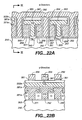
- Figures 16-22 show exemplary sequential cross-sectional views of an integrated circuit structure that illustrate many steps of its formation by a process that corresponds to, but differs in certain respects from, the process described above with respect to Figures 3-9 .
- the process illustrated in Figures 16-22 includes use of narrow source and drain implants (formed differently in Figure 10 ), thickened dielectric layers between the substrate and the select gates (described with respect to Figure 11 ), "T" shaped floating gates (as shown generally by Figure 13B ) and a double dielectric layer between the select gates and the word lines for a reduced coupling between them.
- the reference numbers used in Figures 16-22 for corresponding elements in Figures 3-9 are those of Figures 3-9 with 200 added.
- the semiconductor substrate in Figures 16-22 is labeled "245" while the substrate in Figures 3-9 is labeled "45".
- Figures 16-19 illustrate some of the preliminary processing steps of this second example, as viewed across section II-II (y-direction) of the array of Figure 2 .
- a thin layer 303 of tunnel oxide, about 90 Angstroms thick, for example, is grown on the substrate's surface 301.
- a first layer (P1) of polysilicon about 1000 Angstroms thick is deposited over the layer 303, a layer of silicon nitride about 1000 Angstroms thick then deposited over the polysilicon, and a layer of silicon oxide of about 1500 Angstroms thick is finally deposited over the nitride layer, as a specific example.
- This three layer stack is then etched through a photoresist mask formed on top of the oxide layer (not shown) into strips having lengths extending in the x-direction and being spaced apart in the y-direction.
- the view of Figure 16 is across three such strips in the memory area, polysilicon strips 311, 313 and 315 being formed over the thin oxide layer 301, with similarly shaped strips of the nitride layer 307 and oxide layer 309 on top of the polysilicon.
- a polysilicon strip 317 is shown in the peripheral region of the device, also in an elongated stack with a portion of the nitride layer 307 and oxide layer 309 on top.
- a layer 310 of oxide about 1000 Angstroms thick is deposited over the stacked strips and the spaces between them.
- Another photoresist etch mask is then formed over the layer 310 to completely protect the array but leave the peripheral elements exposed.
- the oxide layer 310 exposed through the mask is then anisotropically etched to remove it from the peripheral region in a manner that leaves a spacer 320 along a side of the stack including the polysilicon layer 317.
- the oxide on the top of the peripheral stack, the spacer 320 and the remaining portion of the oxide layer 310 that was protected by the mask, then serve together as a mask for etching a trench 319 in the substrate 245.
- the trench 319 which can be about 3000 Angstroms deep, for example, serves to isolate the peripheral circuit devices from the memory cell array.
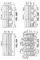
- Figure 17 shows a next series of processing steps.
- the structure is covered with about a 7000 Angstrom layer, as an example, of oxide that fills in the trench 319 and other cavities in the structure, and to a depth over all other elements.
- This thick oxide layer is then removed, preferably by a CMP process, down to the tops of the nitride strips 307, thereby leaving a planar surface 329.
- a next step is to remove the nitride 307 from at least the memory cell array region of the device being formed.
- a second polysilicon layer 330 is then deposited into the voids left by removal of the nitride and over the thick oxide that remains between the polysilicon strips 311, 313 and 315.
- This second polysilicon layer, designated P1' sits on top of the strips formed from the first polysilicon layer, which is designated P1.
- the two polysilicon layers contact each other to effectively form a single polysilicon structure. If this polysilicon has been deposited in an undoped form, as it is in this example, the structure is then exposed to an arsenic ion implant.
- a layer of silicon nitride is deposited to about a 550 Angstrom thickness, for example, over the polysilicon layer 330.
- a mask (not shown) is then formed over the nitride layer and positioned in the y-direction to cover strips of nitride as closely aligned over the polysilicon strips 311, 313 and 315 as possible. Etching of the nitride layer through this mask then leaves the strips 332 elongated in the x-direction but spaced apart in the y-direction.
- This nitride etch mask is not self-aligned with the structure already formed but a slight misalignment does not present a problem.
- spacers 334 are formed along the nitride strips 332. This is done by depositing a layer of nitride about 900 Angstroms thick, in this example, which is then anisotropically etched to remove most of this last layer but leaving the spacers 334. The polysilicon layer 330 is then etched away through the elongated openings between the spacers 334. A small amount of the thick oxide between the polysilicon strips is also preferably removed, as shown in Figure 19 .
- FIGS 20 and 21 are sectional views taken across the x-direction of the array of Figure 2 , at section I-I, perpendicular to the sectional views of Figures 16-19 just described.
- the nitride strips 332 and the spacers 334 are first removed, such as by a wet etch.
- a dielectric layer 348 ( Figure 20 ) is formed, preferably ONO such as one having 50 Angstroms of oxide grown on the polysilicon strips (HTO, high temperature oxide), 150 Angstroms of nitride deposited and then 200 Angstroms of oxide deposited (TEOS).
- ONO such as one having 50 Angstroms of oxide grown on the polysilicon strips (HTO, high temperature oxide), 150 Angstroms of nitride deposited and then 200 Angstroms of oxide deposited (TEOS).
- Reference elements 331, 333 and 335 are then formed over this dielectric layer 348, which are elongated in the y-direction and spaced apart in the x-direction shown in Figure 20 . These reference elements correspond to elements 131, 133 and 135, respectively, of Figure 7A . To form them, a layer of nitride is deposited over the dielectric layer 348, to a depth of 2500 Angstroms, for example. A photoresist mask (not shown) is then formed on top of this nitride layer, through which the nitride layer is etched to leave the reference element strips 331, 333 and 335. These strips need not be registered in the x-direction with any other elements of the structure.
- the spacers 337, 339, 341 and 343 are formed along side them. This is accomplished in this example by a TEOS deposition of BPSG oxide to a depth of about 1800 Angstroms. This layer is then anisotropically etched until all is removed except for the desired spacers.
- the reference elements 331, 333 and 335, and the adjacent spacers 337, 339, 341 and 343 then serve as a mask for etching the polysilicon strips and intermediate thick isolation oxide through the elongated slots between adjacent spacers. That etching step is shown in Figure 20 -to have been accomplished.
- the polysilicon and thick oxide are usually removed in different etching steps with different etchants or processes employed.
- the result of this etching is the individual polysilicon strip segments 315a, 315b and 315c of equal length, with slots elongated in the y-direction that extend through the polysilicon strips and the thick isolation oxide in between.
- a next step is to form a dielectric layer 350 ( Figure 20 ) as a mask that restricts the width of substrate source and drain implants 345 and 347 in the x-direction to something less than a minimum resolution element of the process being employed.
- the layer 350 is preferably formed of TEOS dielectric with a thickness of about 500 Angstroms. This layer adheres to the sidewalls of the polysilicon strip segments, which sidewall portions block the ions from reaching the substrate surface 301, but leaves a space between such sidewall portions through which the ions travel to reach the substrate. These implants are continuous in the y-direction across a large number of polysilicon strip segments.
- the layer 350 is removed by an appropriate process.
- the spacers 337, 339, 341 and 343, plus the portions of the dielectric 348 underlying the spacers, are then removed, leaving the reference elements 333 in place, as shown in Figure 21 .
- a layer of dielectric is then formed over the structure in order to provide interpoly dielectric layers 351 and 353 that extend along exposed polysilicon surfaces within the slots and vertical edges of the nitride reference elements 331, 333 and 335.
- This dielectric is preferably ONO, formed of an oxide layer grown and deposited on the exposed polysilicon and nitride surfaces to a thickness of about 150 Angstroms, followed by depositing about 75 Angstroms of nitride, and then depositing about 50 Angstroms of oxide by HTO. Growth of the initial oxide will be thicker immediately above the regions 345 and 347 implanted in the substrate, thus providing a desired extra degree of isolation between the later formed steering gates and the substrate. The total thickness of the layers 351 and 353 above the implanted regions will typically be about 300 Angstroms, in this example.
- a layer of doped polysilicon (P2) is then deposited over the structure to a depth of about 3000 Angstroms, in this example, which also then extends into the slots lined by the dielectric layers 351 and 353.
- This top portion of this polysilicon is then removed by etching or CMP to the level of the tops of the nitride reference elements 331, 333 and 335. This separates the P2 layer into individual steering gates 381 and 383 that are elongated in the y-direction and spaced apart in the x-direction shown in Figure 21 .
- the structure is oxidized in a manner to grow oxide layers 352 and 354 over the respective doped polysilicon steering gates 381 and 383.
- a next step is to remove the exposed nitride reference elements 331, 333 and 335.
- the polysilicon strip segments 315a, 315b and 315c are then etched through the resulting openings between steering gates, to form slots shown in Figure 22A .
- a dielectric layer 361 is formed along the sidewalls and bottom of these slots. Ions are then typically implanted into the substrate 245 through these slots in order to adjust the thresholds of the resulting select transistors. An additional amount of select gate oxide can then be grown on the bottom of the slots, as part of the dielectric layer 361 shown in Figure 21 .
- the next series of steps form the word lines 292, 293 and 294 ( Figures 22A and 22B ).
- a layer of doped polysilicon is deposited to a thickness of about 3000 Angstroms, in this specific example, which also causes the polysilicon to extend downward into the slots just formed.
- This polysilicon layer is then separated by employing an appropriate photoresist mask and etching step to form the individual word lines.
- the polysilicon of each of the word lines provides the select transistor gates, such as the gate 363 of Figure 22A .
- the select gates 381 and 383 are separated from the word line 292 by two layers of dielectric formed at different times, namely layers 351 and 353 combined with the later formed layer 361.
- This increased thickness dielectric conveniently reduces the amount of coupling between the select gates and the word lines, a desirable result.
- Figure 22B shows the structure at the same point of its processing as Figure 22A but in an orthogonal section. It will be noted that the steering gate lines formed of the polysilicon layer P2 extend down in between the T-shaped floating gates made from the P1 polysilicon layer, thus to provide a shield against excessive coupling between adjacent floating gates that are very closely separated in the y-direction.
- FIG. 23-26 Yet another method of forming the same type of array as described above is illustrated in Figures 23-26 , wherein the "A" portion of each figure is a section of a small portion of the memory cell array being formed, taken at section I-I of Figure 2 (along the x-axis), and the "B" portion of each figure is a section taken at section II-II of Figure 2 (along the y-axis).
- the primary difference between this embodiment and those of the examples described above is that the separation of the first polysilicon strips in the x-direction into individual floating gates occurs during a single masking step, rather than using the nitride reference elements (131, 133, 135 etc.
- Figures 23-26 show only a part of the memory array, peripheral circuit elements may also be included and separated from the array by an oxide filled trench in the substrate, as described for each of the first two specific examples.
- a thin layer 503 of gate dielectric is formed on the surface 501 of the substrate 445, preferably by growing oxide to a thickness of about 90 Angstroms.
- a first layer 515 of polysilicon (P1) is deposited to a thickness of about 1000 Angstroms on the dielectric 503, either doped or undoped followed by an ion-implantation step. This polysilicon is then etched through an appropriate photoresist mask (not shown) into strips 511, 513 and 515 that are elongated in the x-direction and equally spaced apart in the y-direction across the substrate.
- a thick layer of oxide is then deposited over the entire array to fill the spaces between the polysilicon strips and cover them.
- the oxide on top of the polysilicon strips is then removed by etching or CMP to provide a substantially smooth surface, much like such the surface 129 of Figure 6B .
- an interpoly layer 401 of dielectric such as ONO, is formed over that surface.
- a second layer 402 of polysilicon is then deposited over the dielectric layer 401, followed by a layer 403 of oxide being deposited over the polysilicon 402, and a layer 404 of silicon nitride being deposited over the oxide 403.
- the resulting stack of layers shown in Figures 23A and 23B is then etched through another photoresist mask (not shown) to separate the first polysilicon (P1) strips into individual floating gates and separate the stack of layers 401-404 into strips a, b, c and d that are elongated in the y-direction but spaced apart in the x-direction.
- the width of the strips and spaces between them will generally be chosen to have the minimum feature size that is possible with the process that is used to make the circuit structure.
- the dielectric between the P1 strips is etched as well.
- a thin dielectric layer 406 is formed on the sidewalls of the separated strips and the exposed substrate surface, preferably being ONO formed in the same manner as the layers 351 and 351 of the previous example.
- Spacers 407 are then formed on the vertical surfaces by depositing a thick layer of oxide over the structure and then anisotropically etching the oxide away to leave the spacers.
- Source and drain regions 449 and 451 are made by implanting ions into the substrate through every other space between the stacks, the remaining spaces being covered by an appropriate mask (not shown). It is preferable to perform the implantation after the spacers 407 are formed, in order to obtain very narrow implants in the x-direction, but it can be done earlier. Since the spaces between the stacks are continuous across a large extent of the array, continuous source and drain implants are formed that extend in the y-direction across a large number of rows of memory cells.
- a next step is to deposit a third layer of polysilicon over the entire area in order to provide polysilicon in each of the spaces between the spacers 407.
- This polysilicon is then removed by etching to leave strips 410, 411 and 412 (IP) elongated in the y-direction and with top surfaces that lie above the P2 polysilicon layer 402 and below the nitride layer 404.
- IP nitride
- Channels are formed in the oxide and nitride layers 403 and 404 having as depth down to the P2 polysilicon layer 402. These channels are continuous in the y-direction and spaced apart in the x-direction over every other of the intermediate polysilicon (IP) strips. Such channels are shown in Figure 25A to have been made over the intermediate polysilicon strips 410 and 412, while avoiding the region around the intermediate polysilicon strip 411. These channels are preferably formed by etching through a photoresist mask (not shown) on top of the nitride layer 404. The channels are indicated in Figure 25A to be the areas occupied by P2' polysilicon strips 415 and 416, and respective covering oxide layers 417 and 418.
- Another layer of polysilicon is deposited over the surface in order to fill these channels.
- the intermediate spaces such as that occupied by the intermediate polysilicon strip 411, are covered by an appropriate mask (not shown) during this deposition.
- the top of this polysilicon layer is removed down to the top of the nitride layer 404 by etching or CMP. That leaves the formed channels filled with polysilicon strips.
- This polysilicon is then oxidized in order to form protective dielectric layers 417 and 418 on top of the polysilicon strips.
- Exposed intermediate polysilicon surfaces, such as that of the polysilicon strip 411, are preferably covered by another temporary mask during this oxidation step in order to avoid them becoming oxidized.
- the P2' strip 415 is in contact with the P2 polysilicon strips 402a and 402b as well as the intermediate polysilicon strip 410. These elements are each electrically conductive and connected together, both physically and electrically.
- This combination identified in Figure 26A by the reference number 421, provides a steering gate elongated in the y-direction and having capacitive coupling with two adjacent columns of floating gates, including floating gates 455 and 456. A similar composite steering gate 422 is shown.
- the word lines 492-495 are then formed by depositing another layer of polysilicon over the array and etching it to leave the word lines in place. As part of this etching step, the strips of intermediate polysilicon within the alternate spaces between floating gates, such as the strip 411, are also separated to leave individual select transistor gates located under and in mechanical and electrical contact with their respective word lines. Thus, the separated intermediate polysilicon gate elements and the word lines together form strips such as the strip 492 shown in Figure 26A .
- flash EEPROM memory cells have been described with respect to the type of cell that utilizes conductive floating gates as charge storage elements.
- many of the cell structures and processes described above also apply to memory cells that use a charge trapping dielectric as the storage element in place of a floating gate.
- the dielectric is then sandwiched between the control or steering gates and the substrate.
- the dielectric can be separated into individual elements with the same sizes and positions as the floating gates, it is usually not necessary to do so since charge is trapped locally by such a dielectric.
- the charge trapping dielectric can extend over the entire array except in areas occupied by the select transistors.
- the dielectric is formed in strips extending continuously in the y-direction across a large number of rows of cells but individually have a width that is contained between adjacent select transistors in the x-direction. Other regions of the dielectric may be removed in the course of separating the polysilicon layer(s) above the dielectric into its elongated strips without adverse effects but it is not necessity to do so. A portion of the dielectric within each cell that is sandwiched between a conductive gate and the substrate within the cell's channel is then a charge storage element for that cell.
- Dielectric storage element memory cells are generally described in the following technical articles and patent, which articles and patent are incorporated herein in their entirety by this reference: Chan et al., "A True Single-Transistor Oxide-Nitride-Oxide EEPROM Device," IEEE Electron Device Letters, Vol. EDL-8, No. 3, March 1987, pp. 93-95 ; Nozaki et al., "A 1-Mb EEPROM with MONOS Memory Cell for Semiconductor Disk Application,” IEEE Journal of Solid State Circuits, Vol. 26, No. 4, April 1991, pp. 497-501 ; Eitan et al., "NROM: A Novel Localized Trapping, 2-Bit Nonvolatile Memory Cell,” IEEE Electron Device Letters, Vol. 21, No. 11, November 2000, pp. 543-545 , and United States patent no. 5,851,881 .
- charge trapping dielectric materials and configurations There are three specific charge trapping dielectric materials and configurations that can be utilized. One is a two-layer dielectric with oxide grown on the substrate and a layer of silicon nitride deposited thereover ("ON"). Another is a three-layer structure that adds another layer of silicon oxide, grown and/or deposited, over the silicon nitride layer ("ONO"). A third alternative is a single layer of silicon rich silicon dioxide sandwiched between the gate and the semiconductor substrate surface. This later material is described in the following two articles, which articles are incorporated herein in their entirety by this reference: DiMaria et al., "Electrically-alterable read-only-memory using Si-rich SI02 injectors and a floating polycrystalline silicon storage layer," J. Appl. Phys.
Abstract
Description
- This invention relates generally to non-volatile flash memory systems, and, more specifically, to the process of forming memory arrays of memory cells that individually contain two floating gates and the resulting structure.
- There are many commercially successful non-volatile memory products being used today, particularly in the form of small form factor cards, which use an array of flash EEPROM (Electrically Erasable and Programmable Read Only Memory) cells having a "split-channel" between source and drain diffusions. The floating gate of the cell is positioned over one portion of the channel and the word line (also referred to as a control gate) is positioned over the other channel portion as well as over the floating gate. This effectively forms a cell with two transistors in series, one (the memory transistor) with a combination of the amount of charge on the floating gate and the voltage on the word line controlling the amount of current that can flow through its portion of the channel, and the other (the select transistor) having the word line alone serving as its gate. The word line extends over a row of floating gates. Examples of such cells, their uses in memory systems and methods of manufacturing them are given in United States patents nos.
5,070,032 ,5,095,344 ,5,315,541 ,5,343,063 , and5,661,053 , and in co-pending United States patent application serial no.09/239,073, filed January 27, 1999 - A modification of this split-channel flash EEPROM cell adds a steering gate positioned between the floating gate and the word line. Each steering gate of an array extends over one column of floating gates, perpendicular to the word line. The effect is to relieve the word line from having to perform two functions at the same time when reading or programming a selected cell. Those two functions are (1) to serve as a gate of a select transistor, thus requiring a proper voltage to turn the select transistor on and off, and (2) to drive the voltage of the floating gate to a desired level through an electric field (capacitive) coupling between the word line and the floating gate. It is often difficult to perform both of these functions in an optimum manner with a single voltage. With the addition of the steering gate, the word line need only perform function (1), while the added steering gate performs function (2). The use of steering gates in a flash EEPROM array is described, for example, in United States patent nos.
5,313,421 and6,222,762 , which patents incorporated herein by this reference. - In either of the two types of memory cell arrays described above, the floating gate of a cell is programmed by injecting electrons from the substrate to the floating gate. This is accomplished by having the proper doping in the channel region and applying the proper voltages to the source, drain and remaining gate(s). So-called "source side" injection is preferred, which is also described in the foregoing patent no.
5,313,421 . - Two techniques for removing charge from floating gates to erase memory cells are used in both of the two types of memory cell arrays described above. One is to erase to the substrate by applying appropriate voltages to the source, drain and other gate(s) that cause electrons to tunnel through a portion of a dielectric layer between the floating gate and the substrate. The other erase technique is to transfer electrons from the floating gate to another gate through a tunnel dielectric layer positioned between them. In the first type of cell described above, a third erase gate is provided for that purpose. In the second type of cell described above, which already has three gates because of the use of a steering gate, the floating gate is erased to the word line, without the necessity to add a fourth gate. Although this later technique adds back a second function to be performed by the word line, these functions are performed at different times, thus avoiding the necessity of making a compromise because of the two functions. When either erase technique is utilized, a large number of memory cells are grouped together for simultaneously erasure, in a "flash." In one approach, the group includes enough memory cells to store the amount of user data stored in a disk sector, namely 512 bytes, plus some overhead data. In another approach, each group contains enough cells to hold several thousand bytes of user data, equal to many disk sectors' worth of data. Multi-block erasure, defect management and other flash EEPROM system features are described in United States patent no.
5,297,148 , which patent is incorporated herein by this reference. - As in most all integrated circuit applications, the pressure to shrink the silicon substrate area required to implement some integrated circuit function also exists with flash EEPROM systems. It is continually desired to increase the amount of digital data that can be stored in a given area of a silicon substrate, in order to increase the storage capacity of a given size memory card and other types of packages, or to both increase capacity and decrease size. One way to increase the storage density of data is to store more than one bit of data per memory cell. This is accomplished by dividing a window of a floating gate charge level voltage range into more than two states. The use of four such states allows each cell to store two bits of data, eight states stores three bits of data per cell, and so on. A multiple state flash EEPROM structure and operation is described in United States patents nos.
5,043,940 and5,172,338 , which patents are incorporated herein by, this reference. - Increased data density can also be achieved by reducing the physical size of the memory cells and/or the overall array. Shrinking the size of integrated circuits is commonly performed for all types of circuits as processing techniques improve over time to permit implementing smaller feature sizes. But there are usually limits of how far a given circuit layout can be shrunk in this manner, since there is often at least one feature that is limited as to how much it can be shrunk, thus limiting the amount that the overall layout can be shrunk. When this happens, designers will turn to a new or different layout or architecture of the circuit being implemented in order to reduce the amount of silicon area required to perform its functions. The shrinking of the above-described flash EEPROM integrated circuit systems can reach similar limits.
- Therefore, in order to further increase data storage density, a flash EEPROM system using a dual floating gate memory cell is being utilized along with the storage of multiple states on each floating gate. In this type of cell, two floating gates are included over its channel between source and drain diffusions with a select transistor in between them. A steering gate is included along each column of floating gates and a word line is provided thereover along each row of floating gates. When accessing a given floating gate for reading or programming, the steering gate over the other floating gate of the cell containing the floating gate of interest is raised sufficiently high to turn on the channel under the other floating gate no matter what charge level exists on it. This effectively eliminates the other floating gate as a factor in reading or programming the floating gate of interest in the same memory cell. For example, the amount of current flowing through the cell, which can be used to read its state, is then a function of the amount of charge on the floating gate of interest but not of the other floating gate in the same cell. Examples of this cell array architecture and operating techniques are described in United States patent no.
5,712,180 . - According to one aspect of the present invention, a memory array is made by forming a thin layer of dielectric on the substrate surface and then depositing over it a layer of material that is later separated into conductive floating gates. This dielectric layer, which is preferably a grown oxide, remains as the memory cell floating gate dielectric, and is of high quality because of being formed over a virgin substrate surface. This improves the memory erasure operation when the floating gates are erased to the substrate. The floating gate material is preferably doped polysilicon. Continuous source and drain diffusions in the substrate surface extend across rows of floating gates in a columnar direction. Electrical isolation between rows of floating gates is provided by a field dielectric, such as oxide, that is deposited between the rows above the surface of the substrate. Further isolation may be provided by forming a trench into which the field dielectric extends but which is shallow enough to not interrupt the conductivity of the source and drain diffusions that it crosses. Use of continuously conductive diffusions reduces the complexity of the conductive bit lines that connect with the diffusions.
- According to another aspect of the present invention, the area of coupling of a control gate with floating gates is increased by either (1) wrapping the control gate across the top and around the sides of thick floating gates, or (2) increasing the top width of the floating gates that communicates with control gates from a supplemental deposition of conductive material that extends over the floating gates and adjacent dielectric material in at least one direction.
- In another aspect of the present invention, the control gates are formed to extend between adjacent floating gates in order to provide field isolation between them. This allows the floating gates to be packed closer together. In one specific implementation, the floating gates are wider at the top than at the bottom, in order to provide additional area for coupling with the control gates. The floating gates are thus closer together at the top than at the bottom. The control gates extend downward between at least the wider portions of adjacent floating gates, where the need for shielding is the greatest.
- According to a further aspect of the present invention, peripheral circuit elements, such as those of decoders, registers, sense amplifiers, comparators and the like, are isolated from the memory cell array by a trench that is filled with field dielectric, according to a standard Shallow Trench Isolation (STI) technique. Such isolation need not be used within the array itself.
- According to yet another aspect of the present invention, continuous strips of floating gate material are separated into individual floating gates by a single etching operation that is followed by forming substantially the same structure of conductive elements, preferably made of doped polysilicon, in each of the spaces between the floating gates that result from the etching. This method eliminates the need for a second etching of the floating gate material strips in alignment with the first. Every other one of these elements are subsequently joined with additional conductive material to form the steering gates. Word lines are later formed of conductive material to contact the remaining every other one of these elements in one direction across the array that then operate as the select transistor gates.
- The foregoing individual aspects of the present invention, and various other processing improvements described herein, may be implemented by themselves or in various combinations. Another aspect of the present invention is the implementation of one or more of these aspects within a virtual ground array of dual floating gate memory cells, the form of non-volatile memory in which detailed examples of such implementation are described below. Additional aspects, advantages and features of the present invention are included in the following description of these detailed examples, which description should be taken in conjunction with the accompanying drawings.
-
-
Figure 1 illustrates in block diagram form a flash EEPROM system in which the various aspects of the present invention may be implemented; -
Figure 2 is an exemplary plan view of a dual floating gate memory cell array that incorporates the present invention; -
Figures 3A and 3B are sections taken across the memory cell array ofFigure 2 , in respective directions I-I and II-II, at an initial stage of the array's formation, according to a first embodiment; -
Figures 4A and 4B are sections taken across the memory cell array ofFigure 2 , in respective directions I-I and II-II, at a first subsequent stage of the array's formation, according to the first embodiment; -
Figures 5A and 5B are sections taken across the memory cell array ofFigure 2 , in respective directions I-I and II-II, at a second subsequent stage of the array's formation, according to the first embodiment; -
Figures 6A and 6B are sections taken across the memory cell array ofFigure 2 , in respective directions I-I and II-II, at a third subsequent stage of the array's formation, according to the first embodiment; -
Figures 7A and 7B are sections taken across the memory cell array ofFigure 2 , in respective directions I-I and II-II, at a fourth subsequent stage of the array's formation, according to the first embodiment; -
Figures 8A and 8B are sections taken across the memory cell array ofFigure 2 , in respective directions I-I and II-II, at a fifth subsequent stage of the array's formation, according to the first embodiment; -
Figures 9A and 9B are sections taken across the memory cell array ofFigure 2 , in respective directions I-I and II-II, at a sixth subsequent stage of the array's formation, according to the first embodiment; -
Figure 10 illustrates a modification to the process and structure shown inFigure 7A ; -
Figure 11 illustrates a modification to the process and structure shown inFigure 8A ; -
Figures 12A and 12B are sections taken across the memory cell array ofFigure 2 , in respective directions I-I and II-II, and illustrate a modification to the process and structure shown in respectiveFigures 9A and 9B ; -
Figures 13A and 13B are sections taken across the memory cell array ofFigure 2 , in respective directions I-I. and II-II, and illustrate another modification to the process and structure shown in respectiveFigures 9A and 9B ; -
Figures 14A and 14B are sections taken across the memory cell array ofFigure 2 , in respective directions I-I and II-II, and illustrate a modification to the process and structure shown in respectiveFigures 4A and 4B ; -
Figures 15A and 15B are sections taken across the memory cell array ofFigure 2 , in respective directions I-I and II-II, and further illustrate the modification of respectiveFigures 14A and 14B in a later stage corresponding to respectiveFigures 9A and 9B ; -
Figure 16 is a sectional view taken across section II-II the memory cell array ofFigure 2 at a first stage of the array's formation according to a second embodiment; -
Figure 17 is a sectional view taken across section II-II the memory cell array ofFigure 2 at a second stage of the array's formation according to a second embodiment; -
Figure 18 is a sectional view taken across section II-II the memory cell array ofFigure 2 at a third stage of the array's formation according to a second embodiment; -
Figure 19 is a sectional view taken across section II-II the memory cell array ofFigure 2 at a fourth stage of the array's formation according to a second embodiment; -
Figure 20 is a sectional view taken across section I-I the memory cell array ofFigure 2 at a fifth stage of the array's formation according to a second embodiment; -
Figure 21 is a sectional-view taken across section I-I the memory cell array ofFigure 2 at a sixth stage of the array's formation according to a second embodiment; -
Figures 22A and 22B are sections taken across the memory cell array ofFigure 2 , in respective directions I-I and II-II, at a seventh stage of the array's formation, according to the second embodiment; -
Figures 23A and 23B are sections taken across the memory cell array ofFigure 2 , in respective directions I-I and II-II, at a first stage of the array's formation, according to a third embodiment; -
Figures 24A and 24B are sections taken across the memory cell array ofFigure 2 , in respective directions I-I and II-II, at a second stage of the array's formation, according to a third embodiment; -
Figures 25A and 25B are sections taken across the memory cell array ofFigure 2 , in respective directions I-I and II-II, at a third stage of the array's formation, according to a third embodiment; and -
Figures 26A and 26B are sections taken across the memory cell array ofFigure 2 , in respective directions. I-I and II-II, at a fourth stage of the array's formation, according to a third embodiment. - An example memory system incorporating the various aspects of the present invention is generally illustrated in the block diagram of
Figure 1 . A large number of individuallyaddressable memory cells 11 are arranged in a regular array of rows and columns, although other physical arrangements of cells are certainly possible. Bit lines, designated herein to extend along columns of thearray 11 of cells, are electrically connected with a bit line decoder anddriver circuit 13 throughlines 15. Word lines, which are designated in this description to extend along rows of thearray 11 of cells, are electrically connected throughlines 17 to a word line decoder anddriver circuit 19. Steering gates, which extend along columns of memory cells in thearray 11, are electrically connected to a steering gate decoder anddriver circuit 21 throughlines 23. Each of thedecoders bus 25 from amemory controller 27. The decoder and driving circuits are also connected to thecontroller 27 over respective control andstatus signal lines bus 22 that interconnects the decoder anddriver circuits - The
controller 27 is connectable throughlines 35 to a host device (not shown). The host may be a personal computer, notebook computer, digital camera, audio player, various other hand held electronic devices, and the like. The memory system ofFigure 1 will commonly be implemented in a card according to one of several existing physical and electrical standards, such as one from the PCMCIA, the CompactFlash™ Association, the MMC™ Association, and others. When in a card format, thelines 35 terminate in a connector on the card which interfaces with a complementary connector of the host device. The electrical interface of many cards follows the ATA standard, wherein the memory system appears to the host as if it was a magnetic disk drive. Other memory card interface standards also exist. Alternatively to the card format, memory systems of the type shown inFigure 1 are permanently embedded in the host device. - The decoder and
driver circuits array 11, as addressed over thebus 25, according to control signals in respective control andstatus lines array 11 to thecontroller 27 over the same control andstatus lines circuit 13 receive current or voltage levels that are indicative of the states of addressed memory cells within thearray 11, and provides thecontroller 27 with information about those states overlines 41 during a read operation. A large number of sense amplifiers are usually used in order to be able to read the states of a large number of memory cells in parallel. During reading and program operations, one row of cells is typically addressed at a time through thecircuits 19 for accessing a number of cells in the addressed row that are selected by thecircuits - Operation of a memory system such as illustrated in
Figure 1 is further described in patents identified in the Background section above, and in other patents assigned to SanDisk Corporation, assignee of the present application. In addition, United States patent application serial no.09/793,370, filed February 26, 2001 - A plan view of an example
memory cell array 11 is shown inFigure 2 , wherein a small part of its repetitive structure of conductive elements are illustrated with little detail of dielectric layers that exist therebetween. Ausual silicon substrate 45 includes a uniform, preferably substantially planar, top surface 47.Elongated diffusions substrate 45 through the surface 47 by an initial ion implantation and subsequent diffusion, and serve as sources and drains of the memory cells formed between them. In order to provide a convention for this description, the diffusions are shown to be spaced apart in a first x-direction, with lengths extending in a second y-direction, these first and second directions being essentially orthogonal with each other. A large number of floating gates are included across the substrate surface 47 with suitable gate dielectric therebetween, in an array of rows and columns. One row of floating gates 55-60 is adjacent to and parallel with another row of floating gates 62-67, for example, and a column of floatinggates gates diffusions - The bit line decoder and driver circuit 13 (
Figure 1 ) is connected throughlines 15 with all of the bit line source/drain diffusions of the array, including thediffusions Figures 2-4 . The sources and drains of columns of individual memory cells are connected to proper programming voltages for either reading or programming in response to addresses supplied over thebus 25 and control signals over thelines 19. - Rather than employing a separate steering gate for each column of floating gates, the structure of
Figure 2 uses one wider steering gate for every two columns of floating gates. Steeringgates Figure 1 ) connects thoughlines 23 to all the steering gates and is able to individually control their voltages in response to addresses provided on thebus 25, control signals in thelines 33, and data from the drivers andsense amplifiers 13. - Word lines 91-95 of
Figure 2 are elongated in the x-direction and extend over the steering gates with spaces between them in the y-direction that places each word line in alignment with a row of floating gates. The word lines are formed by etching a third layer of conductively doped polysilicon that is deposited over the entire surface on top of a dielectric that is first formed over the second polysilicon layer and regions exposed between the steering gates. The word lines allow selection of all the memory cells in its row for reading or writing. The select gate decoder and driver circuit 19 (Figure 1 ) is connected with each word line in order to individually select one row of the cell array. Individual cells within a selected row are then enabled for reading or writing by the bit line and steering gate decoder anddriver circuits - Although the gates in the foregoing structure are preferably made of doped polysilicon material, other suitable electrically conductive materials may be used in place of one or more of the three polysilicon layers described. The third layer, for example, from which the word lines and select gates are formed, may be a polycide material, which is polysilicon with a conductive refractive metal silicide on its top, such as tungsten, in order to increase its conductivity. Polycides are generally not used in place of either the first or second polysilicon layers because the quality of oxide grown from a polycide is usually not satisfactory.
- Not shown in
Figure 2 are the metal conductor layers. Since the diffusions and polysilicon elements usually have a conductivity that is significantly less than that of metal, metal conductors are included in separate layers, with connections made to respective metal lines through any intermediate layers at periodical intervals along the lengths of the polysilicon elements and diffusions. Since all of the diffusions and polysilicon elements shown inFigure 2 need to be separately driven, there is a one-to-one correspondence between the number of these metal lines and the number of diffusions and polysilicon elements. -
Figures 3-9 illustrate a sequence of steps utilized according to one aspect of the present invention to form the array ofFigure 2 , by showing sectional views ofFigure 2 across sections I-I (part A of each figure) and section II-II (part B of each figure). Referring initially toFigures 3A and 3B , the result of several initial steps in the semiconductor processing are illustrated. A thin (such as 80-100 Angstroms thick)layer 103 of oxide dielectric is grown over theentire surface 101 of thesilicon substrate 45. Next, a thick (such as 500 - 3000 Angstroms)layer 105 of polysilicon is deposited over thedielectric layer 103. The thickness of thelayer 105 is made to be sufficient to provide an amount of coupling along its sidewalls with later formed steering gates that is desired. This polysilicon may be deposited in a doped form or deposited undoped and then doped in a later step by ion implantation. A dielectric layer is then formed over the polysilicon, shown to be two layers. Alayer 107 of silicon nitride is first deposited over thepolysilicon layer 105, followed by the deposition of alayer 109 of silicon oxide over thenitride layer 107. - A next series of steps is illustrated by
Figures 4A and 4B . The oxide layer 109 (Figures 3A and 3B ) is first patterned by the use of an appropriate photoresist mask (not shown) into strips through which the stack oflayers oxide layer 109 as an etch mask, a photoresist etch mask may be formed directly on thesilicon nitride layer 107. - Peripheral transistor and other devices may be formed, at least in part, simultaneously with the processing steps forming the memory cell array.
Figure 4B hows anotherstrip 117 of polysilicon that is left in an area of the integrated circuit where such peripheral devices are being formed. The peripheral devices and the memory array are preferably isolated by atrench 119 in thesubstrate 45 that is positioned between the two areas. Thistrench 119 can be formed by a separate etching step through a photoresist mask. This mask need not necessarily be self aligned with the polysilicon strips. Thetrench 119 can surround, or surround most of the area in which the memory cell array is being formed. Thetrench 119 is preferably made to have a depth of from 1000 - 4000 Angstroms below thesubstrate surface 101. - An
ion implant 121 may be made in the substrate in between the polysilicon strips in the memory cell area at this stage, such as implant strips 123 and 125, using the strips and dielectric on top of them as a mask. This is done as part of providing isolation between memory cell rows. Boron ions are implanted. - As illustrated by
Figures 5A and 5B , a next step is to deposit a very thick layer offield dielectric 127, such as silicon oxide, over the entire circuit structure. This then fills in the spaces between the polysilicon strips 111, 113 and 115, as well as theisolation trench 119. This forms an electrical isolation between the eventual rows of floating gates that are formed from these polysilicon strips. Thetrench 119 and its dielectric filler are formed according to shallow trench isolation (STI) techniques. - A next step, as shown by
Figures 6A and 6B , is to remove the top of thefield dielectric 127 and thedielectric layers planar surface 129, in one example. This is preferably done by a combination of chemical-mechanical-polishing (CMP), which will remove the filed dielectric 127 andoxide strips 109 down to the nitride strips 107 as a stop, and a further etching step to remove the nitride strips 107 and thefield oxide 127 between them. - In subsequent steps illustrated by
Figures 7-9 , the polysilicon strips 111, 113 and 115 are etched twice in order to form the individual floating gates, and the steering gates (elongated in the y-direction) and select gates (part of the word lines elongated in the x-direction) are formed from respective second and third polysilicon layers. This may be done by forming a photoresist mask on thesurface 129 ofFigures 6A and 6B , and etching through it. But this can have the disadvantage of forming elements not totally self aligned with each other. Therefore, the self-aligned technique described with respect toFigures 11-16 of aforementioned incorporated United States patent no.6,103,573 is preferred. This technique is briefly summarized with respect toFigures 7-9 herein, additional details being provided by the incorporated patent. - Referring to
Figures 7A and 7B , a set ofparallel reference elements surface 129, such as by etching a layer of silicon nitride through a photoresist mask.Spacers segments strip 115. Source anddrain implants - Referring to
Figures 8A and 8B , theoxide spacers Layers nitride reference elements isolated steering gates Figure 8A . - A next step is to remove the
nitride reference elements Figures 8A and 8B . The firstpolysilicon layer strips steering gates steering gates nitride reference elements - The resulting openings between the now separated floating gates, such as between floating
gates Figure 9A . Alayer 161 of interpoly dielectric, preferably ONO, is then formed on exposed sides and tops of the floating and steering gates, as well as over exposed substrate areas. Next, a third layer of polysilicon is deposited over the structure and etched through a photoresist mask (not shown) to form strips elongated in the x-direction and spaced apart in the y-direction. These strips are the word lines of the array,word line 92 being shown inFigure 9A . Select transistor gates, such as thegate 163, are formed as part of the word lines in the openings formed between floating gates. - This process has several advantageous features. One is that the floating gates formed from the first polysilicon layer are totally self-aligned with the source and drain diffusions and the steering gates. Another is that the floating
gate oxide layer 103 is of high quality because it is grown on the virgin substrate and then covered by the first polysilicon layer that is later separated into the floating gates. This allows reliably erasing the floating gates to the substrate by a mechanism of tunneling electrons through the gate oxide, as well as programming by the injection of hot electrons onto the floating gates from the substrate through the gate oxide. Yet another advantage is that field oxide deposited on top of the substrate between rows of floating gates provides isolation between these rows, rather than positioning oxide filled trenches formed according to STI between rows. The absence of such deep trenches allows the source and drain diffusions to be formed continuously across multiple rows of cells rather than using isolated diffusions for each cell and then additional polysilicon bit lines to connect the diffusions in a column together. The omission of the isolation trenches further eliminates sharp corners in the substrate that can cause a breakdown of the floating gate dielectric as the result of field concentrations with adjacent floating gates that can tend to wrap around these corners. - There are many variations and additions to the process described above with respect to
Figures 3-9 that can be useful in certain situations. Referring toFigure 10 , for example, a modification to the view ofFigure 7A is given. Prior to making the source and drain implants,dielectric spacers 171 are formed along the side walls of adjacent firstpolysilicon strip.segments spacers 171. As a result, the implant 147' is narrower than theimplant 147 ofFigure 7A . Since the implanted ions will migrate during subsequent processing steps that raise the temperature of the structure, this narrow implant compensates to some degree for such migration in order to maintain a desired width of the final source and drain regions. After the implantation, thespacers 171 are removed, the interpolydielectric layers -
Figure 11 shows another modification of the process, this time with respect toFigure 8A . In order to decrease the coupling between the steering gates and the substrate, athick layer 173 of dielectric is additionally formed in the spaces shown inFigure 7A between the segments of the first polysilicon layer strips. This is done after the source and drain implant has occurred but before the interpolydielectric layers region 173 over the dopedregion 147 of thesilicon substrate surface 101 than on the sides of the polysilicon layer strips 115b and 115c. Since the presence of the dielectric 173 reduces the area of coupling between the steering and floating gates, its depth is controlled in order not to be more than necessary to provide the desired degree of field isolation between the steering gates and the substrate. - However, this area of coupling can be increased by another modification of the basic process that is illustrated in
Figures 12A and 12B . After reaching the stage illustrated inFigure 6B , a portion of the remaining field dielectric between the first polysilicon layer strips 111, 113 and 115 is removed, to leave the reduced amount 127' shown inFigure 12B . The subsequently formed steering gates then wrap around the floating gates in the y-direction. This is shown by the steering gate 81' ofFigure 12B extending down a distance along the sides of the floatinggates Figure 11 but if used together, the increased coupling in the y-direction (Figure 12B ) compensates for the decreased coupling in the x-direction (Figure 11 ). - An alternative technique for increasing the coupling area between the steering and floating gates is illustrated in
Figures 13A and 13B . After reaching the stage shown inFigures 6A and 6B , an additional layer of polysilicon is deposited across thesurface 129 and patterned to leave the additional floating gate portions 111', 113' and 115' on top of, and in contact with, the previously formed floatinggates Figure 13A ) but somewhat longer in the y-direction (Figure 13B ). It is this longer dimension that increases the top area of the floating gate that is coupled with thesteering gate 81 ". Further, the steering gates can be extended down in between the floating gates, as shown inFigure 13B , which provides additional coupling through the edges of the additional floating gate portions. The configuration shown also uses the steering gates to provide shielding between adjacent additional floating gate portions which are closer together in the y-direction than the floating gates without the additional portions. An example technique for forming such T-shaped floating gates is described hereinafter. - Another modification of the process and structure of
Figures 3-9 is illustrated inFigures 14 and 15 . Here, very shallow trenches are etched in the substrate surface between the rows of floating gates and filled with the field oxide that is deposited betweens the rows, in order to increase the degree of electrical isolation between adjacent rows.Figures 14A and 14B correspond, respectively, toFigures 4A and 4B , the difference being the addition of the veryshallow trenches 181 in the substrate 45'. These are most easily formed as an extension of the etching of the first polysilicon layer that is described with respect toFigures 4A and 4B . Thetrenches 181 are preferably made from 500 to 1000 Angstroms deep below the surface 101' of the substrate 45'.Figures 15A and 15B correspond, respectively, withFigures 9A and 9B , and shown the device structure at a later stage of the process. The depth of the trenches 181 (which are elongated in the x-direction) is kept shallow enough that the conduction along the source and drain diffusions (which cross thetrenches 181 in the y-direction) is not significantly affected. - The basic process and structures of
Figures 3-9 may be modified according to one or more of the additional features described with respect toFigures 10-15 , either alone or in various combinations. -
Figures 16-22 show exemplary sequential cross-sectional views of an integrated circuit structure that illustrate many steps of its formation by a process that corresponds to, but differs in certain respects from, the process described above with respect toFigures 3-9 . The process illustrated inFigures 16-22 includes use of narrow source and drain implants (formed differently inFigure 10 ), thickened dielectric layers between the substrate and the select gates (described with respect toFigure 11 ), "T" shaped floating gates (as shown generally byFigure 13B ) and a double dielectric layer between the select gates and the word lines for a reduced coupling between them. The reference numbers used inFigures 16-22 for corresponding elements inFigures 3-9 are those ofFigures 3-9 with 200 added. For example, the semiconductor substrate inFigures 16-22 is labeled "245" while the substrate inFigures 3-9 is labeled "45". -
Figures 16-19 illustrate some of the preliminary processing steps of this second example, as viewed across section II-II (y-direction) of the array ofFigure 2 . Athin layer 303 of tunnel oxide, about 90 Angstroms thick, for example, is grown on the substrate'ssurface 301. A first layer (P1) of polysilicon about 1000 Angstroms thick is deposited over thelayer 303, a layer of silicon nitride about 1000 Angstroms thick then deposited over the polysilicon, and a layer of silicon oxide of about 1500 Angstroms thick is finally deposited over the nitride layer, as a specific example. This three layer stack is then etched through a photoresist mask formed on top of the oxide layer (not shown) into strips having lengths extending in the x-direction and being spaced apart in the y-direction. The view ofFigure 16 is across three such strips in the memory area, polysilicon strips 311, 313 and 315 being formed over thethin oxide layer 301, with similarly shaped strips of thenitride layer 307 andoxide layer 309 on top of the polysilicon. Apolysilicon strip 317 is shown in the peripheral region of the device, also in an elongated stack with a portion of thenitride layer 307 andoxide layer 309 on top. - After that etching is completed and the photoresist mask used to perform it has been removed, a
layer 310 of oxide about 1000 Angstroms thick is deposited over the stacked strips and the spaces between them. Another photoresist etch mask is then formed over thelayer 310 to completely protect the array but leave the peripheral elements exposed. Theoxide layer 310 exposed through the mask is then anisotropically etched to remove it from the peripheral region in a manner that leaves aspacer 320 along a side of the stack including thepolysilicon layer 317. The oxide on the top of the peripheral stack, thespacer 320 and the remaining portion of theoxide layer 310 that was protected by the mask, then serve together as a mask for etching atrench 319 in thesubstrate 245. Thetrench 319, which can be about 3000 Angstroms deep, for example, serves to isolate the peripheral circuit devices from the memory cell array. -
Figure 17 shows a next series of processing steps. The structure is covered with about a 7000 Angstrom layer, as an example, of oxide that fills in thetrench 319 and other cavities in the structure, and to a depth over all other elements. This thick oxide layer is then removed, preferably by a CMP process, down to the tops of the nitride strips 307, thereby leaving aplanar surface 329. This leaves thetrench 319 filled with avolume 327 of oxide, and spaces between the stacks of polysilicon and nitride strips in the memory area also being filled with oxide. - A next step is to remove the
nitride 307 from at least the memory cell array region of the device being formed. As shown inFigure 18 , asecond polysilicon layer 330 is then deposited into the voids left by removal of the nitride and over the thick oxide that remains between the polysilicon strips 311, 313 and 315. This second polysilicon layer, designated P1', sits on top of the strips formed from the first polysilicon layer, which is designated P1. The two polysilicon layers contact each other to effectively form a single polysilicon structure. If this polysilicon has been deposited in an undoped form, as it is in this example, the structure is then exposed to an arsenic ion implant. - With reference to
Figure 19 , the next series of steps are discussed. A layer of silicon nitride is deposited to about a 550 Angstrom thickness, for example, over thepolysilicon layer 330. A mask (not shown) is then formed over the nitride layer and positioned in the y-direction to cover strips of nitride as closely aligned over the polysilicon strips 311, 313 and 315 as possible. Etching of the nitride layer through this mask then leaves thestrips 332 elongated in the x-direction but spaced apart in the y-direction. This nitride etch mask is not self-aligned with the structure already formed but a slight misalignment does not present a problem. - In order to serve as a mask to etch the
polysilicon layer 330 with a line width less than the resolution element of the process being used,spacers 334 are formed along the nitride strips 332. This is done by depositing a layer of nitride about 900 Angstroms thick, in this example, which is then anisotropically etched to remove most of this last layer but leaving thespacers 334. Thepolysilicon layer 330 is then etched away through the elongated openings between thespacers 334. A small amount of the thick oxide between the polysilicon strips is also preferably removed, as shown inFigure 19 . - After this etching, the elongated P1 polysilicon strips are divided into segments along their length and the steering gates formed. This series of processing steps is illustrated in
Figures 20 and 21 , which are sectional views taken across the x-direction of the array ofFigure 2 , at section I-I, perpendicular to the sectional views ofFigures 16-19 just described. The nitride strips 332 and the spacers 334 (Figure 19 ) are first removed, such as by a wet etch. A dielectric layer 348 (Figure 20 ) is formed, preferably ONO such as one having 50 Angstroms of oxide grown on the polysilicon strips (HTO, high temperature oxide), 150 Angstroms of nitride deposited and then 200 Angstroms of oxide deposited (TEOS). -
Reference elements dielectric layer 348, which are elongated in the y-direction and spaced apart in the x-direction shown inFigure 20 . These reference elements correspond toelements Figure 7A . To form them, a layer of nitride is deposited over thedielectric layer 348, to a depth of 2500 Angstroms, for example. A photoresist mask (not shown) is then formed on top of this nitride layer, through which the nitride layer is etched to leave the reference element strips 331, 333 and 335. These strips need not be registered in the x-direction with any other elements of the structure. - After removal of the photoresist material from the top of these strips, the
spacers - The
reference elements adjacent spacers Figure 20 -to have been accomplished. The polysilicon and thick oxide are usually removed in different etching steps with different etchants or processes employed. The result of this etching is the individualpolysilicon strip segments - A next step is to form a dielectric layer 350 (
Figure 20 ) as a mask that restricts the width of substrate source and drainimplants layer 350 is preferably formed of TEOS dielectric with a thickness of about 500 Angstroms. This layer adheres to the sidewalls of the polysilicon strip segments, which sidewall portions block the ions from reaching thesubstrate surface 301, but leaves a space between such sidewall portions through which the ions travel to reach the substrate. These implants are continuous in the y-direction across a large number of polysilicon strip segments. - Next, the
layer 350 is removed by an appropriate process. Thespacers reference elements 333 in place, as shown inFigure 21 . A layer of dielectric is then formed over the structure in order to provide interpolydielectric layers nitride reference elements regions layers - A layer of doped polysilicon (P2) is then deposited over the structure to a depth of about 3000 Angstroms, in this example, which also then extends into the slots lined by the
dielectric layers nitride reference elements individual steering gates Figure 21 . - In order to provide a mask for an additional etch of the first polysilicon layer strip segments and result in additional isolation of the steering gates from the word lines to be later formed, the structure is oxidized in a manner to grow
oxide layers polysilicon steering gates nitride reference elements polysilicon strip segments Figure 22A . Adielectric layer 361 is formed along the sidewalls and bottom of these slots. Ions are then typically implanted into thesubstrate 245 through these slots in order to adjust the thresholds of the resulting select transistors. An additional amount of select gate oxide can then be grown on the bottom of the slots, as part of thedielectric layer 361 shown inFigure 21 . - The next series of steps form the word lines 292, 293 and 294 (
Figures 22A and 22B ). A layer of doped polysilicon is deposited to a thickness of about 3000 Angstroms, in this specific example, which also causes the polysilicon to extend downward into the slots just formed. This polysilicon layer is then separated by employing an appropriate photoresist mask and etching step to form the individual word lines. The polysilicon of each of the word lines provides the select transistor gates, such as thegate 363 ofFigure 22A . - It will be noted from
Figure 22A that theselect gates word line 292 by two layers of dielectric formed at different times, namely layers 351 and 353 combined with the later formedlayer 361. This increased thickness dielectric conveniently reduces the amount of coupling between the select gates and the word lines, a desirable result. -
Figure 22B shows the structure at the same point of its processing asFigure 22A but in an orthogonal section. It will be noted that the steering gate lines formed of the polysilicon layer P2 extend down in between the T-shaped floating gates made from the P1 polysilicon layer, thus to provide a shield against excessive coupling between adjacent floating gates that are very closely separated in the y-direction. - Yet another method of forming the same type of array as described above is illustrated in
Figures 23-26 , wherein the "A" portion of each figure is a section of a small portion of the memory cell array being formed, taken at section I-I ofFigure 2 (along the x-axis), and the "B" portion of each figure is a section taken at section II-II ofFigure 2 (along the y-axis). The primary difference between this embodiment and those of the examples described above is that the separation of the first polysilicon strips in the x-direction into individual floating gates occurs during a single masking step, rather than using the nitride reference elements (131, 133, 135 etc. ofFigures 7 and 8 , and 331, 333, 335 ofFigures 20 and 21 ) to form masks that are aligned during first and second etching steps. After this single etch has occurred, intermediate polysilicon is formed in each of the spaces between floating gates in the x-direction, this intermediate polysilicon becoming part of the steering gates in alternate spaces after some additional processing is performed and becoming gates for the select transistors as part of later completed word lines. The reference number used inFigures 23-26 for elements that correspond to those ofFigures 3-9 are the same as those ofFigures 3-9 with 400 added. For example, the semiconductor substrate inFigures 23-26 is labeled "445" while the substrate inFigures 3-9 is labeled "45". AlthoughFigures 23-26 show only a part of the memory array, peripheral circuit elements may also be included and separated from the array by an oxide filled trench in the substrate, as described for each of the first two specific examples. - Referring to
Figures 23A and 23B , the results of several processing steps are shown. Athin layer 503 of gate dielectric is formed on thesurface 501 of thesubstrate 445, preferably by growing oxide to a thickness of about 90 Angstroms. Afirst layer 515 of polysilicon (P1) is deposited to a thickness of about 1000 Angstroms on the dielectric 503, either doped or undoped followed by an ion-implantation step. This polysilicon is then etched through an appropriate photoresist mask (not shown) intostrips surface 129 ofFigure 6B . - After obtaining such a surface, an
interpoly layer 401 of dielectric, such as ONO, is formed over that surface. Asecond layer 402 of polysilicon is then deposited over thedielectric layer 401, followed by alayer 403 of oxide being deposited over thepolysilicon 402, and alayer 404 of silicon nitride being deposited over theoxide 403. - The resulting stack of layers shown in
Figures 23A and 23B is then etched through another photoresist mask (not shown) to separate the first polysilicon (P1) strips into individual floating gates and separate the stack of layers 401-404 into strips a, b, c and d that are elongated in the y-direction but spaced apart in the x-direction. The width of the strips and spaces between them will generally be chosen to have the minimum feature size that is possible with the process that is used to make the circuit structure. The dielectric between the P1 strips is etched as well. - Next, a
thin dielectric layer 406 is formed on the sidewalls of the separated strips and the exposed substrate surface, preferably being ONO formed in the same manner as thelayers Spacers 407 are then formed on the vertical surfaces by depositing a thick layer of oxide over the structure and then anisotropically etching the oxide away to leave the spacers. Source anddrain regions spacers 407 are formed, in order to obtain very narrow implants in the x-direction, but it can be done earlier. Since the spaces between the stacks are continuous across a large extent of the array, continuous source and drain implants are formed that extend in the y-direction across a large number of rows of memory cells. - A next step is to deposit a third layer of polysilicon over the entire area in order to provide polysilicon in each of the spaces between the
spacers 407. This polysilicon is then removed by etching to leavestrips P2 polysilicon layer 402 and below thenitride layer 404. From every other of the intermediate polysilicon strips across the structure in the x-direction, including theelement 411, is formed a select transistor gate as part of a word line that is later formed. The other intermediate polysilicon elements, such as theelements - The results of several more processing steps are shown in
Figures 25A and 25B . Channels are formed in the oxide andnitride layers P2 polysilicon layer 402. These channels are continuous in the y-direction and spaced apart in the x-direction over every other of the intermediate polysilicon (IP) strips. Such channels are shown inFigure 25A to have been made over the intermediate polysilicon strips 410 and 412, while avoiding the region around theintermediate polysilicon strip 411. These channels are preferably formed by etching through a photoresist mask (not shown) on top of thenitride layer 404. The channels are indicated inFigure 25A to be the areas occupied by P2' polysilicon strips 415 and 416, and respective covering oxide layers 417 and 418. - After the channels are formed, another layer of polysilicon is deposited over the surface in order to fill these channels. The intermediate spaces, such as that occupied by the
intermediate polysilicon strip 411, are covered by an appropriate mask (not shown) during this deposition. The top of this polysilicon layer is removed down to the top of thenitride layer 404 by etching or CMP. That leaves the formed channels filled with polysilicon strips. This polysilicon is then oxidized in order to form protectivedielectric layers 417 and 418 on top of the polysilicon strips. Exposed intermediate polysilicon surfaces, such as that of thepolysilicon strip 411, are preferably covered by another temporary mask during this oxidation step in order to avoid them becoming oxidized. - It will be noted from
Figure 25A that the P2'strip 415 is in contact with theP2 polysilicon strips intermediate polysilicon strip 410. These elements are each electrically conductive and connected together, both physically and electrically. This combination, identified inFigure 26A by thereference number 421, provides a steering gate elongated in the y-direction and having capacitive coupling with two adjacent columns of floating gates, including floatinggates composite steering gate 422 is shown. - The word lines 492-495 are then formed by depositing another layer of polysilicon over the array and etching it to leave the word lines in place. As part of this etching step, the strips of intermediate polysilicon within the alternate spaces between floating gates, such as the
strip 411, are also separated to leave individual select transistor gates located under and in mechanical and electrical contact with their respective word lines. Thus, the separated intermediate polysilicon gate elements and the word lines together form strips such as thestrip 492 shown inFigure 26A . - The foregoing invention summary and specific examples of flash EEPROM memory cells have been described with respect to the type of cell that utilizes conductive floating gates as charge storage elements. However, many of the cell structures and processes described above also apply to memory cells that use a charge trapping dielectric as the storage element in place of a floating gate. When the floating gates are replaced by such a dielectric, the dielectric is then sandwiched between the control or steering gates and the substrate. Although the dielectric can be separated into individual elements with the same sizes and positions as the floating gates, it is usually not necessary to do so since charge is trapped locally by such a dielectric. The charge trapping dielectric can extend over the entire array except in areas occupied by the select transistors. One specific configuration is for the dielectric to be formed in strips extending continuously in the y-direction across a large number of rows of cells but individually have a width that is contained between adjacent select transistors in the x-direction. Other regions of the dielectric may be removed in the course of separating the polysilicon layer(s) above the dielectric into its elongated strips without adverse effects but it is not necessity to do so. A portion of the dielectric within each cell that is sandwiched between a conductive gate and the substrate within the cell's channel is then a charge storage element for that cell.
- Dielectric storage element memory cells are generally described in the following technical articles and patent, which articles and patent are incorporated herein in their entirety by this reference: Chan et al., "A True Single-Transistor Oxide-Nitride-Oxide EEPROM Device," IEEE Electron Device Letters, Vol. EDL-8, No. 3, March 1987, pp. 93-95; Nozaki et al., "A 1-Mb EEPROM with MONOS Memory Cell for Semiconductor Disk Application," IEEE Journal of Solid State Circuits, Vol. 26, No. 4, April 1991, pp. 497-501; Eitan et al., "NROM: A Novel Localized Trapping, 2-Bit Nonvolatile Memory Cell," IEEE Electron Device Letters, Vol. 21, No. 11, November 2000, pp. 543-545, and United States patent no.
5,851,881 . - There are three specific charge trapping dielectric materials and configurations that can be utilized. One is a two-layer dielectric with oxide grown on the substrate and a layer of silicon nitride deposited thereover ("ON"). Another is a three-layer structure that adds another layer of silicon oxide, grown and/or deposited, over the silicon nitride layer ("ONO"). A third alternative is a single layer of silicon rich silicon dioxide sandwiched between the gate and the semiconductor substrate surface. This later material is described in the following two articles, which articles are incorporated herein in their entirety by this reference: DiMaria et al., "Electrically-alterable read-only-memory using Si-rich SI02 injectors and a floating polycrystalline silicon storage layer," J. Appl. Phys. 52(7), July 1981, pp. 4825-4842; Hori et al., "A MOSFET with Si-implanted Gate-Si02 Insulator for Nonvolatile Memory Applications," .
- Although the various aspects of the present invention have been described with respect to specific examples thereof, it will be understood that the invention is entitled to protection within the full scope of the appended claims.
- Further preferred features of the present invention are set out in the following clauses:
- 1. A non-volatile memory, comprising:
- an array of charge storage elements formed on a semiconductor substrate,
- field dielectric material positioned between the charge storage elements in at least one direction across the array, and
- electrically conductive control gates extending across tops of the array of charge storage elements in said at least one direction with a layer of dielectric positioned therebetween and protruding downward into slots formed in the field dielectric between adjacent ones of the charge storage elements, the downward portions of the control gates providing electrical shielding between adjacent charge storage elements in said one direction.
- 2. The memory of
clause 1, wherein the individual charge storage elements have different widths across top and bottom portions thereof in said at least one direction, the top portions being wider than the bottom portions, and the control gates protruding downward therebetween a distance at least as great as a thickness of the top portions. - 3. The memory of
clause 1, wherein the field dielectric is formed over a surface of the semiconductor substrate. - 4. The memory of
clause 1, wherein the array includes the storage elements arranged in a regular pattern of rows and columns, said at least one direction extending along the columns, and wherein the rows include select gates and source/drain regions in the substrate alternately positioned between adjacent storage elements along the rows. - 5. A non-volatile memory, comprising:
- a rectangular array of charge storage elements formed on a substrate surface with a first layer of dielectric therebetween, the individual charge storage elements including a first portion positioned against the first dielectric layer with a first width in one direction across the array and a second portion integrally formed with the first portion a distance removed from the first dielectric layer and with a second width in said one direction, said second width being greater than said first width, and
- elongated electrically conductive control gates extending in said one direction across surfaces of a plurality of charge storage elements furthest removed from the substrate and with a second layer of dielectric therebetween, the control gates additionally extending between adjacent charge storage elements for a distance at least equal to a thickness of the second portion of the charge storage elements, the extensions of the control gates between adjacent charge storage elements providing electrical shielding in said one direction between at least the second portions thereof.
- 6. The non-volatile memory of clause 5, wherein dielectric material fills spaces between the first portions of adjacent ones of the charge storage elements and includes a slot therein into which the control gates extend a distance between the first portions of adjacent charge storage elements.
- 7. The non-volatile memory of clause 6, wherein the dielectric material between the first portions of adjacent ones of the charge storage elements is formed over the substrate surface.
- 8. The non-volatile memory of clause 5, wherein the array includes memory cells that individually include, in a second direction across the array, two charge storage elements between adjacent substrate source and drain regions and a select transistor between the two charge storage elements, said second direction being perpendicular to said one direction.
- 9. A method of forming a non-volatile memory integrated circuit, comprising:
- growing a layer of dielectric across a surface of the substrate,
- depositing a layer of conductive material across the dielectric layer,
- removing a portion of the conductive material layer to form a plurality of slots, which leave conductive material layer strips, elongated in a first direction and spaced apart in a second direction, the first and second directions being orthogonal to each other,
- thereafter depositing field dielectric over and extending into the plurality of slots between the conductive material layer strips, and
- separating the first conductive material layer strips into individual floating gates, thereby forming an array of rows and columns of the floating gates that are individually separated from the substrate surface by the grown layer of dielectric sandwiched therebetween.
- 10. The method of clause 9 additionally comprising forming conductive ion strips in the substrate surface that are elongated in the second direction continuously across a plurality of rows of floating gates and regularly spaced apart in the first direction in between columns of floating gates.
- 11. The method of clause 10, additionally comprising forming trenches elongated in the first direction across a plurality of ion implant regions and spaced apart in the second direction with positions in between the rows of floating gates, and filing the trenches with a dielectric material, the trenches being shallow enough so as not to interrupt the conductivity of the substrate ion strips along their lengths.
- 12. The method of
clause 11, additionally comprising providing peripheral circuits adjacent the array of floating gates, forming at least one trench between the array and the peripheral circuits and filing said at least one trench with a dielectric material, thereby to electrically isolate the array and peripheral circuits, said at least one trench being significantly deeper than the trenches between the rows of floating gates. - 13. The method of clause 9, additionally comprising providing peripheral circuits adjacent the array of floating gates, forming at least one trench between the array and the peripheral circuits and filing said at least one trench with a dielectric material, thereby to electrically isolate the array and peripheral circuits.
- 14. The method of clause 9, wherein depositing the conductive layer includes depositing polysilicon material.
- 15. A method of forming a non-volatile memory array on a substrate, comprising:
- growing a layer of dielectric across a surface of the substrate,
- depositing a first layer of polysilicon across the dielectric layer,
- removing a portion of the first polysilicon layer to form a first plurality of slots, which leave first polysilicon layer strips, elongated in a first direction and spaced apart in a second direction, the first and second directions being orthogonal to each other,
- thereafter depositing field dielectric over and extending into the first plurality of slots between the first polysilicon layer strips,
- removing a top portion of the field dielectric to form a uniform surface across the first polysilicon layer strips, thereby leaving field dielectric between the first polysilicon layer strips in the second direction,
- thereafter removing a portion of the first polysilicon layer strips and field dielectric in a pattern forming a second plurality of slots continuously elongated in the second direction across a plurality of the first polysilicon layer strips and regularly spaced apart in the first direction, thereby separating the first polysilicon layer strips into segments between the second plurality of slots that have equal lengths in the first direction,
- implanting ions into the substrate through the second plurality of slots while the remaining first polysilicon layer strip segments and field oxide act as a mask to block ions from reaching the substrate outside of the second plurality of slots, thereby forming continuous ion strips implanted into the substrate and elongated in the second direction across a plurality of the first polysilicon layer strips,
- thereafter forming, from a second layer of polysilicon deposited over said uniform surface and into the second plurality of slots, steering gates elongated in the second direction and spaced apart in the first direction,
- separating the individual first polysilicon layer strip segments into two floating gates by removing a portion of the first polysilicon layer strip segments exposed between adjacent steering gates, thereby to form spaces between adjacent floating gates, and
- thereafter forming, from a third layer of polysilicon deposited over the steering gates and into the spaces between adjacent floating gates, word lines spaced apart in the second direction and elongated across individual rows of floating gates in the first direction.
- 16. The method of
clause 15, wherein the step of forming steering gates includes using an etch mask over the deposited second polysilicon layer without self- alignment with the second plurality of slots of the first polysilicon layer. - 17. The method of
clause 15, wherein the step of forming steering gates includes orienting the steering gates with spaces between them being self-aligned in the first direction intermediate of adjacent ones of the second plurality of slots in the first polysilicon layer. - 18. The method of
clause 15, wherein removing the first polysilicon layer strips and field oxide in a pattern forming a second plurality of slots includes:- forming first elements of a dielectric mask with lengths oriented in the second direction across the first polysilicon layer strips and field oxide in between and being regularly spaced apart in the first direction, and
- forming dielectric spacers as second elements of the dielectric mask along both sides of the first elements, reducing the width of said second plurality of slots through which the ions are implanted.
- 19. The method of clause 18, wherein forming the steering gates includes:
- after implanting the ions into the substrate, removing the spacers of the dielectric mask while leaving the mask first elements in place,
- depositing the second layer of polysilicon over and between the mask first elements,
- removing any portion of the second layer of polysilicon that is above the mask first elements, and
- thereafter removing the mask first elements, whereby spaces between the steering gates in the first direction are formed.
- 20. The method, of
clause 19, wherein separating the individual first polysilicon layer strip segments includes etching the first polysilicon layer strip segments through the spaces between the steering gates. - 21. The method of clause 20, wherein forming word lines includes depositing, the third layer of polysilicon into the spaces between adjacent floating gates through the spaces between the steering gates.
- 22. The method of
clause 15, wherein removing the top portion of the field dielectric includes using chemical-mechanical-planarization (CMP). - 23. The method of
clause 15, which additionally comprises, after separating the individual first polysilicon layer strip segments into two floating gates, depositing a dielectric material into the spaces formed between adjacent floating gates in a manner to fill a portion of those spaces, the subsequent step of forming word lines including depositing the third layer of polysilicon into the spaces over the deposited dielectric material. - 24. The method of
clause 15, which additionally comprises, after separating the individual first polysilicon layer strip segments into two floating gates, forming recesses in the substrate that are aligned with the spaces between adjacent floating gates, and wherein the subsequent step of forming word lines includes depositing the third layer of polysilicon though the spaces between adjacent floating gates and into the substrate recesses. - 25. The method of
clause 24, wherein separating the first polysilicon layer strip segments into two floating gates additionally includes forming spacers on side walls of the adjacent steering gates in order to reduce the extent of the first polysilicon layer strip segments that are exposed between adjacent steering gates. - 26. The method of
clause 15, which additionally comprises, prior to forming the steering gates, reducing a thickness of the field dielectric between the first polysilicon layer strips to a level below a top surface and a top portion of the sides of the first polysilicon layer strips, and wherein the subsequent formation of the steering gates includes wrapping the steering gates around the top surface and side portion of the sides of the first polysilicon layer strips. - 27. The method of
clause 15, which additionally comprises, prior to implanting ions into the substrate through the second plurality of slots, narrowing a width of the second plurality of slots in the first direction by forming spacers along sides of the second plurality of slots, thereby to subsequently implant ions through the second plurality of slots after being narrowed. - 28. The method of
clause 27, which additionally comprises, after implanting ions into the substrate through the narrowed second plurality of slots, removing the spacers. - 29. The method of
clause 15, which additionally comprises, prior to forming the second plurality of slots, depositing a further layer of polysilicon over the uniform surface and separating the further layer into further strips positioned on top of the first polysilicon layer strips, the further strips being elongated in a first direction and spaced apart in the second direction by a distance that is less than the distance between the first polysilicon layer strips in the second direction, the further strips becoming part of the first polysilicon strips during subsequent processing that forms the second plurality of slots and separates the first polysilicon layer strip segments. - 30. A method of forming a non-volatile memory array on a substrate, comprising:
- growing a layer of dielectric across a surface of the substrate,
- depositing a first layer of polysilicon across the dielectric layer,
- removing a portion of the first polysilicon layer to form a first plurality of slots, which leave first polysilicon layer strips, elongated in a first direction and spaced apart in a second direction, the first and second directions being orthogonal to each other,
- thereafter depositing field dielectric over and extending into the first plurality of slots between the first polysilicon layer strips,
- removing a top portion of the field dielectric to form a uniform surface across the first polysilicon layer strips, thereby leaving field dielectric between the first polysilicon layer strips in the second direction,
- thereafter removing a portion of the first polysilicon layer strips and field dielectric in a pattern forming a second plurality of slots continuously elongated in the second direction across a plurality of the first polysilicon layer strips and regularly spaced apart in the first direction ; thereby separating the first polysilicon layer strips into individual floating gates,
- implanting ions into the substrate through alternate ones of the second plurality of slots, thereby forming continuous ion strips implanted into the substrate and elongated in the second direction across a plurality of rows of floating gates,
- thereafter forming polysilicon elements within the individual second plurality of slots at least between adjacent floating gates,
- forming, from another layer of polysilicon deposited over said uniform surface and in contact with the polysilicon elements within said alternate ones of the second plurality of slots, steering gates elongated in the second direction and spaced apart in the first direction, and
- forming, from a further layer of polysilicon deposited over the steering gates and in contact with the polysilicon elements within others of the second plurality of slots than said alternate ones, word lines spaced apart in the second direction and elongated across individual rows of floating gates in the first direction.
- 31. A non-volatile memory formed on an integrated circuit substrate, comprising:
- an array of memory cells formed in a first region of the substrate,
- circuits peripheral to the memory cell array including decoders, drivers and sense amplifiers that are formed in a second region of the substrate that does not overlap the first region, and
- a trench formed in the substrate between the first and second regions, the trench being at least 3000 Angstroms in depth and filled with a dielectric material, thereby to isolate the memory cell array and peripheral circuits.
Claims (16)
- A method of forming a non-volatile memory array on a substrate, the method comprising:growing a layer of dielectric across a surface of the substrate;depositing a first layer of polysilicon across the dielectric layer;removing a portion of the first polysilicon layer to form a first plurality of slots, which leave first polysilicon layer strips, elongated in a first direction and spaced apart in a second direction, the first and second directions being orthogonal to each other;thereafter depositing field dielectric over and extending into the first plurality of slots between the first polysilicon layer strips;removing a top portion of the field dielectric to form a uniform surface across the first polysilicon layer strips, thereby leaving field dielectric between the first polysilicon layer strips in the second direction;thereafter removing a portion of the first polysilicon layer strips and field dielectric in a pattern forming a second plurality of slots continuously elongated in the second direction across a plurality of the first polysilicon layer strips and regularly spaced apart in the first direction, thereby separating the first polysilicon layer strips into segments between the second plurality of slots;implanting ions into the substrate through at least some of the second plurality of slots while the remaining first polysilicon layer strip segments and field oxide act as a mask to block ions from reaching the substrate outside of those slots, thereby forming continuous ion strips implanted into the substrate and elongated in the second direction across a plurality of the first polysilicon layer strips;thereafter forming, from a second layer of polysilicon deposited over said uniform surface and into the second plurality of slots, steering gates elongated in the second direction and spaced apart in the first direction;separating the individual first polysilicon layer strip segments into two floating gates by removing a portion of the first polysilicon layer strip segments exposed between adjacent steering gates, thereby to form spaces between adjacent floating gates; andthereafter forming, from a third layer of polysilicon deposited over the steering gates and into the spaces between adjacent floating gates, word lines spaced apart in the second direction and elongated across individual rows of floating gates in the first direction.
- The method of claim 1, wherein the step of forming steering gates includes using an etch mask over the deposited second polysilicon layer without self-alignment with the second plurality of slots of the first polysilicon layer.
- The method of any preceding claim, wherein forming the steering gates includes orienting the steering gates with spaces between them being self-aligned in the first direction intermediate of adjacent ones of the second plurality of slots in the first polysilicon layer.
- The method of any preceding claim, which additionally comprises, prior to forming the second plurality of slots, depositing a further layer of polysilicon over the uniform surface and separating the further layer into further strips positioned on top of the first polysilicon layer strips, the further strips being elongated in a first direction and spaced apart in the second direction by a distance that is less than the distance between the first polysilicon layer strips in the second direction, the further strips becoming part of the first polysilicon strips during subsequent processing that forms the second plurality of slots and separates the first polysilicon layer strip segments.
- The method of any preceding claim, which additionally comprises, prior to forming the steering gates, reducing a thickness of the field dielectric between the first polysilicon layer strips to a level below a top surface and a top portion of the sides of the first polysilicon layer strips, and wherein the subsequent formation of the steering gates includes wrapping the steering gates around the top surface and side portion of the sides of the first polysilicon layer strips.
- The method of any preceding claim, wherein removing the first polysilicon layer strips and field oxide in a pattern forming a second plurality of slots includes:forming first elements of a dielectric mask with lengths oriented in the second direction across the first polysilicon layer strips and field oxide in between and being regularly spaced apart in the first direction; andforming dielectric spacers as second elements of the dielectric mask along both sides of the first elements, reducing the width of said second plurality of slots through which the ions are implanted.
- The method of claim 6, wherein forming the steering gates includes:after implanting the ions into the substrate, removing the spacers of the dielectric mask while leaving the mask first elements in place, depositing the second layer of polysilicon over and between the mask first elements, removing any portion of the second layer of polysilicon that is above the mask first elements, and thereafter removing the mask first elements, whereby spaces between the steering gates in the first direction are formed.
- The method, of claim 7, wherein separating the individual first polysilicon layer strip segments includes etching the first polysilicon layer strip segments through the spaces between the steering gates; and
wherein forming word lines includes depositing the third layer of polysilicon into the spaces between adjacent floating gates through the spaces between the steering gates. - The method of any preceding claim, wherein implanting the ions into the substrate through at least some of the second plurality of slots includes implanting the ions through each of the second plurality of slots.
- The method of any preceding claim, further comprising:separating each of the first polysilicon layer strip segments into two floating gates by removing a portion of the first polysilicon layer strip segments exposed between adjacent steering gates.
- The method of claim 10, further comprising:after separating the individual first polysilicon layer strip segments into two floating gates, depositing a dielectric material into the spaces formed between adjacent floating gates in a manner to fill a portion of those spaces, the subsequent step of forming word lines including depositing the third layer of polysilicon into the spaces over the deposited dielectric material.
- The method of any one of claims 10-11, further comprising:after separating the individual first polysilicon layer strip segments into two floating gates, forming recesses in the substrate that are aligned with the spaces between adjacent floating gates, and wherein the subsequent forming of the word lines includes depositing the third layer of polysilicon though the spaces between adjacent floating gates and into the substrate recesses.
- The method of claim 12, wherein separating the first polysilicon layer strip segments into two floating gates additionally includes forming spacers on side walls of the adjacent steering gates in order to reduce the extent of the first polysilicon layer strip segments that are exposed between adjacent steering gates.
- The method of any one of claims 1-8, wherein removing a portion of the first polysilicon layer strips into segments includes separating the first polysilicon layer strips into segments that are individual floating gates.
- The method of any one of claims 1-8 and 14, wherein implanting the ions into the substrate through at least some of the second plurality of slots includes implanting the ions through alternate ones of the second plurality of slots.
- The method of claim 15, wherein the word lines are formed to be in contact with the polysilicon elements within others of the second plurality of slots than said alternate ones.
Applications Claiming Priority (2)
| Application Number | Priority Date | Filing Date | Title |
|---|---|---|---|
| US09/925,102 US6762092B2 (en) | 2001-08-08 | 2001-08-08 | Scalable self-aligned dual floating gate memory cell array and methods of forming the array |
| EP02759287A EP1415346A2 (en) | 2001-08-08 | 2002-08-07 | Floating gate memory array and methods of forming |
Related Parent Applications (1)
| Application Number | Title | Priority Date | Filing Date |
|---|---|---|---|
| EP02759287.2 Division | 2002-08-07 |
Publications (2)
| Publication Number | Publication Date |
|---|---|
| EP2267774A2 true EP2267774A2 (en) | 2010-12-29 |
| EP2267774A3 EP2267774A3 (en) | 2011-10-12 |
Family
ID=25451228
Family Applications (2)
| Application Number | Title | Priority Date | Filing Date |
|---|---|---|---|
| EP10010263A Withdrawn EP2267774A3 (en) | 2001-08-08 | 2002-08-07 | Method of forming a floating-gate memory array |
| EP02759287A Withdrawn EP1415346A2 (en) | 2001-08-08 | 2002-08-07 | Floating gate memory array and methods of forming |
Family Applications After (1)
| Application Number | Title | Priority Date | Filing Date |
|---|---|---|---|
| EP02759287A Withdrawn EP1415346A2 (en) | 2001-08-08 | 2002-08-07 | Floating gate memory array and methods of forming |
Country Status (8)
| Country | Link |
|---|---|
| US (4) | US6762092B2 (en) |
| EP (2) | EP2267774A3 (en) |
| JP (1) | JP4753536B2 (en) |
| KR (2) | KR100965112B1 (en) |
| CN (1) | CN100578793C (en) |
| AU (1) | AU2002324633A1 (en) |
| TW (1) | TW560049B (en) |
| WO (1) | WO2003015173A2 (en) |
Families Citing this family (70)
| Publication number | Priority date | Publication date | Assignee | Title |
|---|---|---|---|---|
| US6762092B2 (en) * | 2001-08-08 | 2004-07-13 | Sandisk Corporation | Scalable self-aligned dual floating gate memory cell array and methods of forming the array |
| DE10153384B4 (en) * | 2001-10-30 | 2007-08-02 | Infineon Technologies Ag | Semiconductor memory cell, method for its production and semiconductor memory device |
| US6925007B2 (en) | 2001-10-31 | 2005-08-02 | Sandisk Corporation | Multi-state non-volatile integrated circuit memory systems that employ dielectric storage elements |
| US6542407B1 (en) * | 2002-01-18 | 2003-04-01 | Sandisk Corporation | Techniques of recovering data from memory cells affected by field coupling with adjacent memory cells |
| JP2003218244A (en) * | 2002-01-24 | 2003-07-31 | Seiko Epson Corp | Method of manufacturing semiconductor device |
| EP1514309B1 (en) * | 2002-06-19 | 2013-11-27 | SanDisk Technologies Inc. | Deep wordline trench to shield cross coupling between adjacent cells of nand memory |
| US6894930B2 (en) * | 2002-06-19 | 2005-05-17 | Sandisk Corporation | Deep wordline trench to shield cross coupling between adjacent cells for scaled NAND |
| US7843899B2 (en) * | 2002-09-20 | 2010-11-30 | Avaya Inc. | Apparatus and method for providing call status information |
| US6908817B2 (en) | 2002-10-09 | 2005-06-21 | Sandisk Corporation | Flash memory array with increased coupling between floating and control gates |
| US6888755B2 (en) * | 2002-10-28 | 2005-05-03 | Sandisk Corporation | Flash memory cell arrays having dual control gates per memory cell charge storage element |
| US6944063B2 (en) | 2003-01-28 | 2005-09-13 | Sandisk Corporation | Non-volatile semiconductor memory with large erase blocks storing cycle counts |
| US7550800B2 (en) * | 2003-06-06 | 2009-06-23 | Chih-Hsin Wang | Method and apparatus transporting charges in semiconductor device and semiconductor memory device |
| US7759719B2 (en) | 2004-07-01 | 2010-07-20 | Chih-Hsin Wang | Electrically alterable memory cell |
| US7613041B2 (en) | 2003-06-06 | 2009-11-03 | Chih-Hsin Wang | Methods for operating semiconductor device and semiconductor memory device |
| US7105406B2 (en) * | 2003-06-20 | 2006-09-12 | Sandisk Corporation | Self aligned non-volatile memory cell and process for fabrication |
| US6979857B2 (en) * | 2003-07-01 | 2005-12-27 | Micron Technology, Inc. | Apparatus and method for split gate NROM memory |
| US7221008B2 (en) | 2003-10-06 | 2007-05-22 | Sandisk Corporation | Bitline direction shielding to avoid cross coupling between adjacent cells for NAND flash memory |
| US7183153B2 (en) * | 2004-03-12 | 2007-02-27 | Sandisk Corporation | Method of manufacturing self aligned non-volatile memory cells |
| US6989320B2 (en) * | 2004-05-11 | 2006-01-24 | Advanced Micro Devices, Inc. | Bitline implant utilizing dual poly |
| JP2006054283A (en) * | 2004-08-11 | 2006-02-23 | Nec Electronics Corp | Nonvolatile semiconductor memory device and its manufacturing method |
| US7064030B2 (en) * | 2004-10-08 | 2006-06-20 | Freescale Semiconductor, Inc. | Method for forming a multi-bit non-volatile memory device |
| US20060076604A1 (en) * | 2004-10-08 | 2006-04-13 | Prinz Erwin J | Virtual ground memory array and method therefor |
| US7518179B2 (en) * | 2004-10-08 | 2009-04-14 | Freescale Semiconductor, Inc. | Virtual ground memory array and method therefor |
| US7638850B2 (en) | 2004-10-14 | 2009-12-29 | Saifun Semiconductors Ltd. | Non-volatile memory structure and method of fabrication |
| US7381615B2 (en) * | 2004-11-23 | 2008-06-03 | Sandisk Corporation | Methods for self-aligned trench filling with grown dielectric for high coupling ratio in semiconductor devices |
| US7402886B2 (en) * | 2004-11-23 | 2008-07-22 | Sandisk Corporation | Memory with self-aligned trenches for narrow gap isolation regions |
| US7482223B2 (en) * | 2004-12-22 | 2009-01-27 | Sandisk Corporation | Multi-thickness dielectric for semiconductor memory |
| US7266787B2 (en) * | 2005-02-24 | 2007-09-04 | Icera, Inc. | Method for optimising transistor performance in integrated circuits |
| US20060190893A1 (en) * | 2005-02-24 | 2006-08-24 | Icera Inc. | Logic cell layout architecture with shared boundary |
| US7411244B2 (en) | 2005-06-28 | 2008-08-12 | Chih-Hsin Wang | Low power electrically alterable nonvolatile memory cells and arrays |
| US7786512B2 (en) * | 2005-07-18 | 2010-08-31 | Saifun Semiconductors Ltd. | Dense non-volatile memory array and method of fabrication |
| US7619275B2 (en) * | 2005-07-25 | 2009-11-17 | Freescale Semiconductor, Inc. | Process for forming an electronic device including discontinuous storage elements |
| US7642594B2 (en) * | 2005-07-25 | 2010-01-05 | Freescale Semiconductor, Inc | Electronic device including gate lines, bit lines, or a combination thereof |
| US7582929B2 (en) * | 2005-07-25 | 2009-09-01 | Freescale Semiconductor, Inc | Electronic device including discontinuous storage elements |
| US7619270B2 (en) * | 2005-07-25 | 2009-11-17 | Freescale Semiconductor, Inc. | Electronic device including discontinuous storage elements |
| US7112490B1 (en) * | 2005-07-25 | 2006-09-26 | Freescale Semiconductor, Inc. | Hot carrier injection programmable structure including discontinuous storage elements and spacer control gates in a trench |
| US7670902B2 (en) * | 2005-07-26 | 2010-03-02 | Semiconductor Manufacturing International (Shanghai) Corporation | Method and structure for landing polysilicon contact |
| US7541240B2 (en) * | 2005-10-18 | 2009-06-02 | Sandisk Corporation | Integration process flow for flash devices with low gap fill aspect ratio |
| US20070120180A1 (en) * | 2005-11-25 | 2007-05-31 | Boaz Eitan | Transition areas for dense memory arrays |
| KR100711000B1 (en) * | 2005-11-28 | 2007-04-24 | 동부일렉트로닉스 주식회사 | Mos transistor equipped with double gate and the manufacturing method thereof |
| US7592224B2 (en) | 2006-03-30 | 2009-09-22 | Freescale Semiconductor, Inc | Method of fabricating a storage device including decontinuous storage elements within and between trenches |
| US7951669B2 (en) | 2006-04-13 | 2011-05-31 | Sandisk Corporation | Methods of making flash memory cell arrays having dual control gates per memory cell charge storage element |
| US7572699B2 (en) * | 2007-01-24 | 2009-08-11 | Freescale Semiconductor, Inc | Process of forming an electronic device including fins and discontinuous storage elements |
| US7838922B2 (en) * | 2007-01-24 | 2010-11-23 | Freescale Semiconductor, Inc. | Electronic device including trenches and discontinuous storage elements |
| US7651916B2 (en) * | 2007-01-24 | 2010-01-26 | Freescale Semiconductor, Inc | Electronic device including trenches and discontinuous storage elements and processes of forming and using the same |
| US7745285B2 (en) | 2007-03-30 | 2010-06-29 | Sandisk Corporation | Methods of forming and operating NAND memory with side-tunneling |
| JP2008283095A (en) * | 2007-05-14 | 2008-11-20 | Toshiba Corp | Nonvolatile semiconductor memory device and method of manufacturing the same |
| US8320191B2 (en) | 2007-08-30 | 2012-11-27 | Infineon Technologies Ag | Memory cell arrangement, method for controlling a memory cell, memory array and electronic device |
| US7681164B2 (en) * | 2007-08-31 | 2010-03-16 | Synopsys, Inc. | Method and apparatus for placing an integrated circuit device within an integrated circuit layout |
| US7829936B2 (en) * | 2007-10-17 | 2010-11-09 | Spansion Llc | Split charge storage node inner spacer process |
| US8072023B1 (en) | 2007-11-12 | 2011-12-06 | Marvell International Ltd. | Isolation for non-volatile memory cell array |
| US8120088B1 (en) | 2007-12-07 | 2012-02-21 | Marvell International Ltd. | Non-volatile memory cell and array |
| US7759201B2 (en) * | 2007-12-17 | 2010-07-20 | Sandisk 3D Llc | Method for fabricating pitch-doubling pillar structures |
| JP5328145B2 (en) * | 2007-12-24 | 2013-10-30 | ラピスセミコンダクタ株式会社 | Nonvolatile memory device and manufacturing method thereof |
| US7981592B2 (en) * | 2008-04-11 | 2011-07-19 | Sandisk 3D Llc | Double patterning method |
| US7786015B2 (en) * | 2008-04-28 | 2010-08-31 | Sandisk 3D Llc | Method for fabricating self-aligned complementary pillar structures and wiring |
| US20090273015A1 (en) * | 2008-04-30 | 2009-11-05 | Atmel Corporation | Non-volatile memory cell |
| US7732235B2 (en) | 2008-06-30 | 2010-06-08 | Sandisk 3D Llc | Method for fabricating high density pillar structures by double patterning using positive photoresist |
| US7781269B2 (en) * | 2008-06-30 | 2010-08-24 | Sandisk 3D Llc | Triangle two dimensional complementary patterning of pillars |
| US8076056B2 (en) * | 2008-10-06 | 2011-12-13 | Sandisk 3D Llc | Method of making sub-resolution pillar structures using undercutting technique |
| US8080443B2 (en) * | 2008-10-27 | 2011-12-20 | Sandisk 3D Llc | Method of making pillars using photoresist spacer mask |
| US8084347B2 (en) | 2008-12-31 | 2011-12-27 | Sandisk 3D Llc | Resist feature and removable spacer pitch doubling patterning method for pillar structures |
| US8114765B2 (en) * | 2008-12-31 | 2012-02-14 | Sandisk 3D Llc | Methods for increased array feature density |
| US7846756B2 (en) * | 2008-12-31 | 2010-12-07 | Sandisk 3D Llc | Nanoimprint enhanced resist spacer patterning method |
| US8692310B2 (en) | 2009-02-09 | 2014-04-08 | Spansion Llc | Gate fringing effect based channel formation for semiconductor device |
| US8026178B2 (en) * | 2010-01-12 | 2011-09-27 | Sandisk 3D Llc | Patterning method for high density pillar structures |
| US7923305B1 (en) | 2010-01-12 | 2011-04-12 | Sandisk 3D Llc | Patterning method for high density pillar structures |
| EP2532005A4 (en) | 2010-02-07 | 2016-06-22 | Zeno Semiconductor Inc | Semiconductor memory device having electrically floating body transistor, and having both volatile and non-volatile functionality and method |
| US8759908B2 (en) * | 2011-11-01 | 2014-06-24 | Alpha And Omega Semiconductor Incorporated | Two-dimensional shielded gate transistor device and method of manufacture |
| US20160181435A1 (en) * | 2014-12-22 | 2016-06-23 | Wafertech, Llc | Floating gate transistors and method for forming the same |
Citations (13)
| Publication number | Priority date | Publication date | Assignee | Title |
|---|---|---|---|---|
| US5043940A (en) | 1988-06-08 | 1991-08-27 | Eliyahou Harari | Flash EEPROM memory systems having multistate storage cells |
| US5070032A (en) | 1989-03-15 | 1991-12-03 | Sundisk Corporation | Method of making dense flash eeprom semiconductor memory structures |
| US5095344A (en) | 1988-06-08 | 1992-03-10 | Eliyahou Harari | Highly compact eprom and flash eeprom devices |
| US5172338A (en) | 1989-04-13 | 1992-12-15 | Sundisk Corporation | Multi-state EEprom read and write circuits and techniques |
| US5297148A (en) | 1989-04-13 | 1994-03-22 | Sundisk Corporation | Flash eeprom system |
| US5313421A (en) | 1992-01-14 | 1994-05-17 | Sundisk Corporation | EEPROM with split gate source side injection |
| US5315541A (en) | 1992-07-24 | 1994-05-24 | Sundisk Corporation | Segmented column memory array |
| US5343063A (en) | 1990-12-18 | 1994-08-30 | Sundisk Corporation | Dense vertical programmable read only memory cell structure and processes for making them |
| US5661053A (en) | 1994-05-25 | 1997-08-26 | Sandisk Corporation | Method of making dense flash EEPROM cell array and peripheral supporting circuits formed in deposited field oxide with the use of spacers |
| US5712180A (en) | 1992-01-14 | 1998-01-27 | Sundisk Corporation | EEPROM with split gate source side injection |
| US5851881A (en) | 1997-10-06 | 1998-12-22 | Taiwan Semiconductor Manufacturing Company, Ltd. | Method of making monos flash memory for multi-level logic |
| US6103573A (en) | 1999-06-30 | 2000-08-15 | Sandisk Corporation | Processing techniques for making a dual floating gate EEPROM cell array |
| US6222762B1 (en) | 1992-01-14 | 2001-04-24 | Sandisk Corporation | Multi-state memory |
Family Cites Families (84)
| Publication number | Priority date | Publication date | Assignee | Title |
|---|---|---|---|---|
| US610357A (en) * | 1898-09-06 | The norbis petcrs co | ||
| US5268319A (en) | 1988-06-08 | 1993-12-07 | Eliyahou Harari | Highly compact EPROM and flash EEPROM devices |
| US5198380A (en) | 1988-06-08 | 1993-03-30 | Sundisk Corporation | Method of highly compact EPROM and flash EEPROM devices |
| US5168465A (en) | 1988-06-08 | 1992-12-01 | Eliyahou Harari | Highly compact EPROM and flash EEPROM devices |
| US5268318A (en) | 1988-06-08 | 1993-12-07 | Eliyahou Harari | Highly compact EPROM and flash EEPROM devices |
| US5053839A (en) | 1990-01-23 | 1991-10-01 | Texas Instruments Incorporated | Floating gate memory cell and device |
| IT1243303B (en) | 1990-07-24 | 1994-05-26 | Sgs Thomson Microelectronics | DEPLOYING OF MEMORY CELLS WITH METAL LINES OF SOURCE AND DRAIN CONNECTION FORMED ON THE SUBSTRATE AND ORTHOGONALLY OVERLAYED BY LINES OF GATE CONNECTION AND PROCEDURE FOR ITS MANUFACTURE |
| US5512505A (en) | 1990-12-18 | 1996-04-30 | Sandisk Corporation | Method of making dense vertical programmable read only memory cell structure |
| US20080079059A1 (en) | 1991-04-24 | 2008-04-03 | Eon Silicon Solution Inc. | Method of manufacturing a nonvolatile semiconductor memory device and select gate device having a stacked gate structure |
| JP2750986B2 (en) * | 1992-10-27 | 1998-05-18 | 尚茂 玉蟲 | Insulated gate electrostatic induction thyristor with split gate type cathode short circuit structure |
| US5471423A (en) * | 1993-05-17 | 1995-11-28 | Nippon Steel Corporation | Non-volatile semiconductor memory device |
| US5604032A (en) | 1993-10-19 | 1997-02-18 | Matsushita Electric Industrial Co., Ltd. | Fluorine-containing carboxylic acid amine salt and a magnetic recording medium with the same thereon |
| WO1995022837A1 (en) * | 1994-02-17 | 1995-08-24 | National Semiconductor Corporation | A method for reducing the spacing between the horizontally-adjacent floating gates of a flash eprom array |
| US5756385A (en) | 1994-03-30 | 1998-05-26 | Sandisk Corporation | Dense flash EEPROM cell array and peripheral supporting circuits formed in deposited field oxide with the use of spacers |
| US5640032A (en) | 1994-09-09 | 1997-06-17 | Nippon Steel Corporation | Non-volatile semiconductor memory device with improved rewrite speed |
| US5498560A (en) | 1994-09-16 | 1996-03-12 | Motorola, Inc. | Process for forming an electrically programmable read-only memory cell |
| JP2655124B2 (en) * | 1995-03-06 | 1997-09-17 | 日本電気株式会社 | Nonvolatile semiconductor memory device and method of manufacturing the same |
| EP0827608B1 (en) | 1995-05-23 | 1998-11-11 | Daimler-Benz Aktiengesellschaft | Process for the computer-assisted measurement and testing of electric circuits, especially electronic modules, and testing station for implementing the process |
| US5579259A (en) | 1995-05-31 | 1996-11-26 | Sandisk Corporation | Low voltage erase of a flash EEPROM system having a common erase electrode for two individually erasable sectors |
| US5680345A (en) | 1995-06-06 | 1997-10-21 | Advanced Micro Devices, Inc. | Nonvolatile memory cell with vertical gate overlap and zero birds beaks |
| DE19525070C2 (en) | 1995-07-10 | 2001-12-06 | Infineon Technologies Ag | Electrically writable and erasable read-only memory cell arrangement and method for the production thereof |
| JP3366173B2 (en) | 1995-07-31 | 2003-01-14 | シャープ株式会社 | Manufacturing method of nonvolatile semiconductor memory |
| US5712179A (en) | 1995-10-31 | 1998-01-27 | Sandisk Corporation | Method of making triple polysilicon flash EEPROM arrays having a separate erase gate for each row of floating gates |
| KR0179163B1 (en) | 1995-12-26 | 1999-03-20 | 문정환 | Method of manufacturing non-volatile memory cell |
| US5903495A (en) | 1996-03-18 | 1999-05-11 | Kabushiki Kaisha Toshiba | Semiconductor device and memory system |
| KR100192551B1 (en) | 1996-05-16 | 1999-06-15 | 구본준 | Semiconductor memory device and fabrication method of the same |
| US5786988A (en) | 1996-07-02 | 1998-07-28 | Sandisk Corporation | Integrated circuit chips made bendable by forming indentations in their back surfaces flexible packages thereof and methods of manufacture |
| US5751038A (en) | 1996-11-26 | 1998-05-12 | Philips Electronics North America Corporation | Electrically erasable and programmable read only memory (EEPROM) having multiple overlapping metallization layers |
| JP3512976B2 (en) | 1997-03-21 | 2004-03-31 | 株式会社東芝 | Nonvolatile semiconductor memory device and method of manufacturing the same |
| US5915167A (en) | 1997-04-04 | 1999-06-22 | Elm Technology Corporation | Three dimensional structure memory |
| JPH10320988A (en) | 1997-05-23 | 1998-12-04 | Sony Corp | Semiconductor non-volatile memory device, its data programming method and its manufacture |
| JP4330670B2 (en) * | 1997-06-06 | 2009-09-16 | 株式会社東芝 | Nonvolatile semiconductor memory device |
| JP3602691B2 (en) * | 1997-06-27 | 2004-12-15 | 株式会社東芝 | Nonvolatile semiconductor memory device and method of manufacturing the same |
| JP3583583B2 (en) | 1997-07-08 | 2004-11-04 | 株式会社東芝 | Semiconductor device and manufacturing method thereof |
| JP3540579B2 (en) | 1997-11-07 | 2004-07-07 | 株式会社東芝 | Semiconductor storage device and method of manufacturing the same |
| US5867429A (en) | 1997-11-19 | 1999-02-02 | Sandisk Corporation | High density non-volatile flash memory without adverse effects of electric field coupling between adjacent floating gates |
| US5981335A (en) | 1997-11-20 | 1999-11-09 | Vanguard International Semiconductor Corporation | Method of making stacked gate memory cell structure |
| JP3447939B2 (en) | 1997-12-10 | 2003-09-16 | 株式会社東芝 | Nonvolatile semiconductor memory and data reading method |
| JPH11186419A (en) * | 1997-12-25 | 1999-07-09 | Toshiba Corp | Non-volatile semiconductor storage device |
| US6069382A (en) * | 1998-02-11 | 2000-05-30 | Cypress Semiconductor Corp. | Non-volatile memory cell having a high coupling ratio |
| JP4056611B2 (en) | 1998-03-17 | 2008-03-05 | 富士通株式会社 | Nonvolatile semiconductor memory device and method for reproducing memory data of nonvolatile semiconductor memory device |
| US6403421B1 (en) | 1998-04-22 | 2002-06-11 | Sony Corporation | Semiconductor nonvolatile memory device and method of producing the same |
| JP3298509B2 (en) * | 1998-06-12 | 2002-07-02 | 日本電気株式会社 | Method for manufacturing semiconductor device |
| JP2000024076A (en) * | 1998-07-08 | 2000-01-25 | Kazuko Tsutsumi | Blood circulation promoting bag |
| KR100297712B1 (en) | 1998-07-23 | 2001-08-07 | 윤종용 | Nonvolatile memory for high integration & fabricating method the same |
| KR100284739B1 (en) * | 1998-09-25 | 2001-05-02 | 윤종용 | Method of manufacturing non-volatile memory device |
| JP3866460B2 (en) | 1998-11-26 | 2007-01-10 | 株式会社東芝 | Nonvolatile semiconductor memory device |
| TW399288B (en) | 1998-12-24 | 2000-07-21 | United Microelectronics Corp | Structure of flash memory and the manufacturing method thereof |
| US6281075B1 (en) | 1999-01-27 | 2001-08-28 | Sandisk Corporation | Method of controlling of floating gate oxide growth by use of an oxygen barrier |
| EP1703520B1 (en) * | 1999-02-01 | 2011-07-27 | Renesas Electronics Corporation | Semiconductor integrated circuit and nonvolatile memory element |
| US6256225B1 (en) * | 1999-02-26 | 2001-07-03 | Micron Technology, Inc. | Construction and application for non-volatile reprogrammable switches |
| US6159801A (en) | 1999-04-26 | 2000-12-12 | Taiwan Semiconductor Manufacturing Company | Method to increase coupling ratio of source to floating gate in split-gate flash |
| US6151248A (en) * | 1999-06-30 | 2000-11-21 | Sandisk Corporation | Dual floating gate EEPROM cell array with steering gates shared by adjacent cells |
| KR20010004990A (en) * | 1999-06-30 | 2001-01-15 | 김영환 | Flash EEPROM cell and method of manufacturing the same |
| US6235586B1 (en) | 1999-07-13 | 2001-05-22 | Advanced Micro Devices, Inc. | Thin floating gate and conductive select gate in situ doped amorphous silicon material for NAND type flash memory device applications |
| EP1104023A1 (en) | 1999-11-26 | 2001-05-30 | STMicroelectronics S.r.l. | Process for manufacturing electronic devices comprising non-volatile memory cells |
| US6518618B1 (en) | 1999-12-03 | 2003-02-11 | Intel Corporation | Integrated memory cell and method of fabrication |
| JP2001168306A (en) | 1999-12-09 | 2001-06-22 | Toshiba Corp | Non-volatile semiconductor memory device and its manufacturing method |
| KR100317488B1 (en) | 1999-12-28 | 2001-12-24 | 박종섭 | Method of manufacturing a flash memory device |
| JP2002026151A (en) * | 2000-07-05 | 2002-01-25 | Mitsubishi Electric Corp | Semiconductor memory device |
| US6529410B1 (en) | 2000-09-20 | 2003-03-04 | Advanced Micro Devices, Inc. | NAND array structure and method with buried layer |
| US6512263B1 (en) | 2000-09-22 | 2003-01-28 | Sandisk Corporation | Non-volatile memory cell array having discontinuous source and drain diffusions contacted by continuous bit line conductors and methods of forming |
| TW457713B (en) * | 2000-10-06 | 2001-10-01 | Winbond Electronics Corp | Manufacturing method of EEPROM cell |
| JP3984020B2 (en) | 2000-10-30 | 2007-09-26 | 株式会社東芝 | Nonvolatile semiconductor memory device |
| KR100389918B1 (en) | 2000-11-14 | 2003-07-04 | 삼성전자주식회사 | Highly integrated non-volatile memory cell array having high program speed |
| US6654217B2 (en) * | 2000-12-29 | 2003-11-25 | Square D Company | Quick responding instantaneous trip system |
| US6738289B2 (en) | 2001-02-26 | 2004-05-18 | Sandisk Corporation | Non-volatile memory with improved programming and method therefor |
| US6559009B2 (en) * | 2001-03-29 | 2003-05-06 | Macronix International Co. Ltd. | Method of fabricating a high-coupling ratio flash memory |
| KR100598092B1 (en) | 2001-05-18 | 2006-07-07 | 삼성전자주식회사 | Flash Memory and Method Of Forming The Same |
| JP2002359308A (en) | 2001-06-01 | 2002-12-13 | Toshiba Corp | Semiconductor memory and its fabricating method |
| US6522580B2 (en) | 2001-06-27 | 2003-02-18 | Sandisk Corporation | Operating techniques for reducing effects of coupling between storage elements of a non-volatile memory operated in multiple data states |
| US6762092B2 (en) | 2001-08-08 | 2004-07-13 | Sandisk Corporation | Scalable self-aligned dual floating gate memory cell array and methods of forming the array |
| EP1514309B1 (en) | 2002-06-19 | 2013-11-27 | SanDisk Technologies Inc. | Deep wordline trench to shield cross coupling between adjacent cells of nand memory |
| US6894930B2 (en) | 2002-06-19 | 2005-05-17 | Sandisk Corporation | Deep wordline trench to shield cross coupling between adjacent cells for scaled NAND |
| US6770932B2 (en) | 2002-07-10 | 2004-08-03 | Kabushiki Kaisha Toshiba | Semiconductor memory device having a memory region and a peripheral region, and a manufacturing method thereof |
| US6888755B2 (en) | 2002-10-28 | 2005-05-03 | Sandisk Corporation | Flash memory cell arrays having dual control gates per memory cell charge storage element |
| JP3927156B2 (en) | 2003-02-26 | 2007-06-06 | 株式会社東芝 | Nonvolatile semiconductor memory device |
| JP4005962B2 (en) | 2003-09-22 | 2007-11-14 | 株式会社東芝 | Nonvolatile semiconductor memory device |
| US7154779B2 (en) | 2004-01-21 | 2006-12-26 | Sandisk Corporation | Non-volatile memory cell using high-k material inter-gate programming |
| US7355237B2 (en) | 2004-02-13 | 2008-04-08 | Sandisk Corporation | Shield plate for limiting cross coupling between floating gates |
| US7183153B2 (en) | 2004-03-12 | 2007-02-27 | Sandisk Corporation | Method of manufacturing self aligned non-volatile memory cells |
| US7385015B2 (en) | 2004-10-12 | 2008-06-10 | Exxonmobil Chemical Patents Inc. | Trialkylaluminum treated supports |
| JP4521366B2 (en) | 2006-02-22 | 2010-08-11 | 株式会社東芝 | Nonvolatile semiconductor memory device and method for manufacturing nonvolatile semiconductor memory device |
| US7615445B2 (en) | 2006-09-21 | 2009-11-10 | Sandisk Corporation | Methods of reducing coupling between floating gates in nonvolatile memory |
-
2001
- 2001-08-08 US US09/925,102 patent/US6762092B2/en not_active Expired - Lifetime
-
2002
- 2002-08-06 TW TW091117683A patent/TW560049B/en not_active IP Right Cessation
- 2002-08-07 JP JP2003519998A patent/JP4753536B2/en not_active Expired - Fee Related
- 2002-08-07 EP EP10010263A patent/EP2267774A3/en not_active Withdrawn
- 2002-08-07 WO PCT/US2002/025025 patent/WO2003015173A2/en active Application Filing
- 2002-08-07 CN CN02815618A patent/CN100578793C/en not_active Expired - Lifetime
- 2002-08-07 KR KR1020047002026A patent/KR100965112B1/en active IP Right Grant
- 2002-08-07 KR KR1020107006235A patent/KR101032266B1/en not_active IP Right Cessation
- 2002-08-07 AU AU2002324633A patent/AU2002324633A1/en not_active Abandoned
- 2002-08-07 EP EP02759287A patent/EP1415346A2/en not_active Withdrawn
-
2004
- 2004-03-12 US US10/799,180 patent/US6953970B2/en not_active Expired - Fee Related
-
2005
- 2005-04-20 US US11/111,129 patent/US7211866B2/en not_active Expired - Fee Related
-
2007
- 2007-03-22 US US11/689,775 patent/US7858472B2/en not_active Expired - Lifetime
Patent Citations (14)
| Publication number | Priority date | Publication date | Assignee | Title |
|---|---|---|---|---|
| US5095344A (en) | 1988-06-08 | 1992-03-10 | Eliyahou Harari | Highly compact eprom and flash eeprom devices |
| US5043940A (en) | 1988-06-08 | 1991-08-27 | Eliyahou Harari | Flash EEPROM memory systems having multistate storage cells |
| US5070032A (en) | 1989-03-15 | 1991-12-03 | Sundisk Corporation | Method of making dense flash eeprom semiconductor memory structures |
| US5172338A (en) | 1989-04-13 | 1992-12-15 | Sundisk Corporation | Multi-state EEprom read and write circuits and techniques |
| US5297148A (en) | 1989-04-13 | 1994-03-22 | Sundisk Corporation | Flash eeprom system |
| US5172338B1 (en) | 1989-04-13 | 1997-07-08 | Sandisk Corp | Multi-state eeprom read and write circuits and techniques |
| US5343063A (en) | 1990-12-18 | 1994-08-30 | Sundisk Corporation | Dense vertical programmable read only memory cell structure and processes for making them |
| US5712180A (en) | 1992-01-14 | 1998-01-27 | Sundisk Corporation | EEPROM with split gate source side injection |
| US5313421A (en) | 1992-01-14 | 1994-05-17 | Sundisk Corporation | EEPROM with split gate source side injection |
| US6222762B1 (en) | 1992-01-14 | 2001-04-24 | Sandisk Corporation | Multi-state memory |
| US5315541A (en) | 1992-07-24 | 1994-05-24 | Sundisk Corporation | Segmented column memory array |
| US5661053A (en) | 1994-05-25 | 1997-08-26 | Sandisk Corporation | Method of making dense flash EEPROM cell array and peripheral supporting circuits formed in deposited field oxide with the use of spacers |
| US5851881A (en) | 1997-10-06 | 1998-12-22 | Taiwan Semiconductor Manufacturing Company, Ltd. | Method of making monos flash memory for multi-level logic |
| US6103573A (en) | 1999-06-30 | 2000-08-15 | Sandisk Corporation | Processing techniques for making a dual floating gate EEPROM cell array |
Non-Patent Citations (5)
| Title |
|---|
| CHAN ET AL.: "A True Single-Transistor Oxide-Nitride-Oxide EEPROM Device", IEEE ELECTRON DEVICE LETTERS, vol. EDL-8, no. 3, March 1987 (1987-03-01), pages 93 - 95 |
| DIMARIA ET AL.: "Electrically-alterable read-only-memory using Si-rich SI02 injectors and a floating polycrystalline silicon storage layer", J. APPL. PHYS., vol. 52, no. 7, July 1981 (1981-07-01), pages 4825 - 4842, XP001400364 |
| EITAN ET AL.: "NROM: A Novel Localized Trapping, 2-Bit Nonvolatile Memory Cell", IEEE ELECTRON DEVICE LETTERS, vol. 21, no. 11, November 2000 (2000-11-01), pages 543 - 545, XP011430532, DOI: doi:10.1109/55.877205 |
| HORI ET AL.: "A MOSFET with Si-implanted Gate-Si02 Insulator for Nonvolatile Memory Applications", IEDM, vol. 92, April 1992 (1992-04-01), pages 469 - 472 |
| NOZAKI ET AL.: "A 1-Mb EEPROM with MONOS Memory Cell for Semiconductor Disk Application", IEEE JOURNAL OF SOLID STATE CIRCUITS, vol. 26, no. 4, April 1991 (1991-04-01), pages 497 - 501 |
Also Published As
| Publication number | Publication date |
|---|---|
| KR101032266B1 (en) | 2011-05-06 |
| US20040095797A1 (en) | 2004-05-20 |
| US7858472B2 (en) | 2010-12-28 |
| JP4753536B2 (en) | 2011-08-24 |
| US7211866B2 (en) | 2007-05-01 |
| JP2004538644A (en) | 2004-12-24 |
| US6762092B2 (en) | 2004-07-13 |
| KR100965112B1 (en) | 2010-06-23 |
| EP2267774A3 (en) | 2011-10-12 |
| KR20100051728A (en) | 2010-05-17 |
| CN1543676A (en) | 2004-11-03 |
| US20070161191A1 (en) | 2007-07-12 |
| EP1415346A2 (en) | 2004-05-06 |
| US20040175888A1 (en) | 2004-09-09 |
| KR20040035732A (en) | 2004-04-29 |
| AU2002324633A1 (en) | 2003-02-24 |
| TW560049B (en) | 2003-11-01 |
| US6953970B2 (en) | 2005-10-11 |
| CN100578793C (en) | 2010-01-06 |
| WO2003015173A3 (en) | 2004-02-19 |
| US20050201154A1 (en) | 2005-09-15 |
| WO2003015173A2 (en) | 2003-02-20 |
Similar Documents
| Publication | Publication Date | Title |
|---|---|---|
| US6953970B2 (en) | Scalable self-aligned dual floating gate memory cell array and methods of forming the array | |
| US7183153B2 (en) | Method of manufacturing self aligned non-volatile memory cells | |
| US6420231B1 (en) | Processing techniques for making a dual floating gate EEPROM cell array | |
| US7541237B2 (en) | Non-volatile memory cell array having discontinuous source and drain diffusions contacted by continuous bit line conductors and methods of forming | |
| EP1636834B1 (en) | Method of forming an array of memory cells comprising floating-gate structures with vertical projections | |
| US7491999B2 (en) | Non-volatile memory cells utilizing substrate trenches |
Legal Events
| Date | Code | Title | Description |
|---|---|---|---|
| PUAI | Public reference made under article 153(3) epc to a published international application that has entered the european phase |
Free format text: ORIGINAL CODE: 0009012 |
|
| 17P | Request for examination filed |
Effective date: 20101019 |
|
| AC | Divisional application: reference to earlier application |
Ref document number: 1415346 Country of ref document: EP Kind code of ref document: P |
|
| AK | Designated contracting states |
Kind code of ref document: A2 Designated state(s): AT BE BG CH CY CZ DE DK EE ES FI FR GB GR IE IT LI LU MC NL PT SE SK TR |
|
| PUAL | Search report despatched |
Free format text: ORIGINAL CODE: 0009013 |
|
| AK | Designated contracting states |
Kind code of ref document: A3 Designated state(s): AT BE BG CH CY CZ DE DK EE ES FI FR GB GR IE IT LI LU MC NL PT SE SK TR |
|
| RIC1 | Information provided on ipc code assigned before grant |
Ipc: H01L 21/28 20060101ALI20110908BHEP Ipc: H01L 27/115 20060101AFI20110908BHEP Ipc: H01L 29/788 20060101ALI20110908BHEP Ipc: H01L 29/423 20060101ALI20110908BHEP Ipc: H01L 21/8247 20060101ALI20110908BHEP |
|
| RAP1 | Party data changed (applicant data changed or rights of an application transferred) |
Owner name: SANDISK TECHNOLOGIES INC. |
|
| 17Q | First examination report despatched |
Effective date: 20130403 |
|
| STAA | Information on the status of an ep patent application or granted ep patent |
Free format text: STATUS: THE APPLICATION IS DEEMED TO BE WITHDRAWN |
|
| 18D | Application deemed to be withdrawn |
Effective date: 20130814 |