EP2267802A2 - High efficiency group III nitride LED with lenticular surface - Google Patents
High efficiency group III nitride LED with lenticular surface Download PDFInfo
- Publication number
- EP2267802A2 EP2267802A2 EP10185898A EP10185898A EP2267802A2 EP 2267802 A2 EP2267802 A2 EP 2267802A2 EP 10185898 A EP10185898 A EP 10185898A EP 10185898 A EP10185898 A EP 10185898A EP 2267802 A2 EP2267802 A2 EP 2267802A2
- Authority
- EP
- European Patent Office
- Prior art keywords
- diode
- light emitting
- lenticular
- group iii
- led
- Prior art date
- Legal status (The legal status is an assumption and is not a legal conclusion. Google has not performed a legal analysis and makes no representation as to the accuracy of the status listed.)
- Withdrawn
Links
Images


Classifications
-
- H—ELECTRICITY
- H01—ELECTRIC ELEMENTS
- H01L—SEMICONDUCTOR DEVICES NOT COVERED BY CLASS H10
- H01L33/00—Semiconductor devices with at least one potential-jump barrier or surface barrier specially adapted for light emission; Processes or apparatus specially adapted for the manufacture or treatment thereof or of parts thereof; Details thereof
- H01L33/005—Processes
- H01L33/0062—Processes for devices with an active region comprising only III-V compounds
- H01L33/0066—Processes for devices with an active region comprising only III-V compounds with a substrate not being a III-V compound
- H01L33/007—Processes for devices with an active region comprising only III-V compounds with a substrate not being a III-V compound comprising nitride compounds
-
- H—ELECTRICITY
- H01—ELECTRIC ELEMENTS
- H01L—SEMICONDUCTOR DEVICES NOT COVERED BY CLASS H10
- H01L33/00—Semiconductor devices with at least one potential-jump barrier or surface barrier specially adapted for light emission; Processes or apparatus specially adapted for the manufacture or treatment thereof or of parts thereof; Details thereof
- H01L33/02—Semiconductor devices with at least one potential-jump barrier or surface barrier specially adapted for light emission; Processes or apparatus specially adapted for the manufacture or treatment thereof or of parts thereof; Details thereof characterised by the semiconductor bodies
- H01L33/20—Semiconductor devices with at least one potential-jump barrier or surface barrier specially adapted for light emission; Processes or apparatus specially adapted for the manufacture or treatment thereof or of parts thereof; Details thereof characterised by the semiconductor bodies with a particular shape, e.g. curved or truncated substrate
- H01L33/22—Roughened surfaces, e.g. at the interface between epitaxial layers
-
- H—ELECTRICITY
- H01—ELECTRIC ELEMENTS
- H01L—SEMICONDUCTOR DEVICES NOT COVERED BY CLASS H10
- H01L33/00—Semiconductor devices with at least one potential-jump barrier or surface barrier specially adapted for light emission; Processes or apparatus specially adapted for the manufacture or treatment thereof or of parts thereof; Details thereof
- H01L33/44—Semiconductor devices with at least one potential-jump barrier or surface barrier specially adapted for light emission; Processes or apparatus specially adapted for the manufacture or treatment thereof or of parts thereof; Details thereof characterised by the coatings, e.g. passivation layer or anti-reflective coating
Definitions
- the present invention relates to light emitting diodes ("LEDs”) and in particular relates to high-brightness light emitting diodes formed from Group III nitride active structures on silicon carbide substrates.
- Solid state devices because of their nature and operation, are inherently much more reliable than earlier generations of electronic devices and can have significantly longer lifetimes, typically by a factor of at least 100. In comparison to such mature technologies, solid-state devices are longer-lasting, physically more rugged, use less power, and are more efficient.
- a light emitting diode is a p-n junction semiconductor diode that emits light when current is injected across a p-n junction (forward biased) to drive the recombination of electrons and holes with the concurrent production of photons.
- light emitting diodes produce light based upon the movement of electrons in a semiconductor material. Therefore, LEDs do not require (although they can be used in conjunction with) vapors or phosphors. They share the desirable characteristics of most semiconductor-based devices, including high efficiency (their emissions comparatively little heat), high reliability and long life. For example, typical LEDs have a mean time between failures of between about 100,000 and 1,000,000 hours meaning that a conservative half lifetime for an LED is on the order of 50,000 hours.
- An LED's emitted light has a frequency (which in turn relates directly to wavelength and color in accordance with well-understood principles of physics) based upon the energy difference between permitted energy levels in the material, a characteristic referred to as the bandgap.
- the bandgap is a fundamental property of the semiconductor material and its doping.
- gallium arsenide phosphide (GaAsP) represents a well-established material system for light emitting diodes. Depending on the mole fraction of Ga and As, these materials have a bandgap of between about 1.42 and 1.98 electron volts (eV), and will emit light in the infrared, red and orange portions of the electromagnetic spectrum.
- red, orange and yellow In order to further commercialize light emitting diode applications, however, colors other than red, orange and yellow must be available. Specifically blue and green light emitting diodes are required (along with red diodes) to create white light or full color displays. Because these colors represent higher-energy portions of the visible spectrum, they require larger transitions than the bandgaps of silicon or gallium arsenide can provide.
- Such materials include diamond (5.47 eV), silicon carbide (2.99 eV) and Group III nitrides such as GaN (3.4 eV).
- wide bandgap LEDs can be combined with red and green LEDs to produce white light, or with phosphors that produce white light when excited by blue or UV light, or both.
- the Group III nitride compositions i.e., Group III of the periodic table
- GaN, AlGaN, InGaN and AlInGaN are particularly useful for LEDs that emit in the ultraviolet (UV) through green portions of the spectrum.
- they are "direct" bandgap materials, meaning that when an electron transition occurs across the bandgap, much of the energy is emitted as light.
- indirect materials such as silicon carbide
- Group III nitrides offer efficiency advantages over indirect transition materials.
- the bandgap of ternary and quaternary Group III materials depends upon the atomic fraction of the included Group III elements.
- the wavelength (color) of the emission can be tailored (within limits) by controlling the atomic fraction of each Group III element in a ternary or quaternary nitride.
- GaP gallium-arsenide or gallium phosphide
- blue and UV-emitting LEDs have lagged behind GaP-based LED's in their commercial appearance.
- silicon carbide is physically very hard, has no melt phase, and requires high temperatures (on the order of about 1500-2000 °C) for epitaxial or sublimation growth.
- the Group III nitrides have relatively large nitrogen vapor pressures at their melting temperatures and thus are likewise difficult or impossible to grow from a melt.
- Blue LEDs and their related derivative devices are becoming more frequently included in consumer electronic devices, particularly small displays. Common examples include items such as computer screens, personal digital assistants ("PDAs”) and cellular phones. In turn, these small devices drive demand for thinner LEDs with reduced area (“footprint”). Such LEDs, however, must still operate at low forward voltages (V f ) and high light output. To date, however, reducing the size of the Group III nitride devices has tended to increase their forward voltage and reduce their radiant flux.
- the Group III nitride light emitting diodes have the potential to provide replacement for long-standing illumination technologies such as incandescent and fluorescent lighting. Historically, however, LEDs have lacked brightness comparable to incandescent, fluorescent or vapor-discharge lights and thus these older technologies have continued to occupy the field. Only recently, have white LEDs (or LED-based white-emitting devices) begun to make inroads into commercial lighting applications, with most of these being in smaller applications such as flashlights and related items.
- Silicon carbide can also be conductively doped. This provides advantages in comparison to sapphire based Group III nitride diodes. Because sapphire is an insulator, two top wire bonds are typically required to mount a working sapphire-based diode. In comparison, silicon carbide devices can be "vertically" oriented; i.e., with ohmic contacts on opposite ends of the device. Such vertical orientation is directly analogous to diodes formed in other conductive semiconductor materials such as gallium arsenide (GaAs), and thus the same mounting orientations and techniques can be used.
- GaAs gallium arsenide
- silver epoxy is a mixture of more than about 50 percent by weight of microscopic silver particles with epoxy resin precursors.
- epoxy resin precursors When used to connect electronic devices to circuits (or circuit boards) the silver epoxy provides flexibility, relative ease of handling, conductivity and good heat transfer properties. Because silver epoxy is (purposely) applied as a viscous liquid, it can and will flow accordingly and, unless other steps are taken, will tend to surround lower portions of any diode mounted with it. As noted above, if the active portions are adjacent the lead frame, the flowing silver epoxy can contact the active portion and cause short circuiting or other undesired interactions.
- the inverted device can be positioned on some sort of sub-structure, with the sub-structure being attached to the lead frame.
- sub-structure examples include U.S. Patent Application Publication No. 20030213965 .
- the sub-structure is included to add sufficient thickness to remove the active portions farther from the lead frame and its silver epoxy or related materials.
- soldering the device to a substructure can undesirably tilt the device with respect to the sub-structure and thereby exacerbate the short-circuiting problem.
- the invention is a high efficiency Group III nitride light emitting diode that includes a substrate selected from the group consisting of semiconducting and conducting materials, a Group III nitride-based light emitting region on the substrate; and a lenticular surface containing single crystal silicon carbide on the light emitting region.
- the invention is a high efficiency Group III nitride light emitting diode that includes a conductive silicon carbide substrate; an aluminum indium gallium nitride light emitting region on the substrate, and a thin lenticular surface of silicon carbide on the light emitting region.
- the invention is a high efficiency Group III nitride light emitting diode that includes a substrate selected from the group consisting of conducting and semiconducting materials, at least one metal bonding layer on one surface of the substrate, an ohmic contact to the opposite surface of the substrate from the metal layer, a light emitting structure based upon the Group III nitride system on the at least one metal layer on the substrate, an ohmic contact on the light emitting structure opposite the substrate, and a lenticular surface, at least portions of which are formed of silicon carbide, on the portions of the light emitting structure other than the ohmic contact.
- the invention is a high efficiency Group III nitride light emitting diode that includes a silicon carbide substrate, a backside ohmic contact on one surface of the substrate for providing one electrical connection to the diode, a metal bonding layer on the opposite surface of the substrate for providing a physical and electronic transition between the substrate and other portions of the diode, a mirror layer on the metal bonding layer for enhancing light extraction from the diode, a p-type Group III nitride layer on the mirror, a light emitting Group III nitride layer on the p-type layer and having a bandgap smaller than the bandgap of the p-type layer, an n-type Group III nitride layer on the light emitting layer and having a bandgap larger than the bandgap of the light emitting layer, a wire bond pad ohmic contact to the n-type layer for providing a second electrical connection to the diode, and a lenticular surface, at
- the invention is a high-efficiency Group III nitride light emitting diode package that includes a lead frame, and a light emitting diode on the lead frame, the diode including, a substrate selected from the group consisting of semiconducting and conducting materials, a Group III nitride based light emitting region on the substrate, a lenticular surface containing single crystal silicon carbide on the light emitting region, an ohmic contact between the substrate and the lead frame, and an ohmic contact to the light emitting region.
- the invention is a wafer structure for high efficiency Group III nitride light emitting diode precursors that includes a conductive silicon carbide substrate wafer, a Group III nitride epitaxial layer on the substrate, a plurality of discrete ohmic contacts on the surface of the Group III nitride epitaxial layer, the ohmic contacts defining a plurality of discrete light emitting diode precursors, and a lenticular surface containing single crystals silicon carbide on the Group III nitride epitaxial layer.
- Figure 1 is a cross sectional schematic illustration of a diode according to the present invention.
- Figure 2 is a cross sectional schematic illustration of a second embodiment of a diode according to the present invention.
- Figure 3 is a cross-sectional schematic illustration of a third embodiment of a diode according to the present invention.
- Figure 4 is a schematic cross-sectional illustration of a diode and a lead frame in accordance with the present invention.
- Figure 5 is a cross sectional schematic diagram of a semiconductor wafer in accordance with the present invention.
- Figure 6 is a scanning electron microscope (SEM) photograph of a diode according to the present invention.
- Figures 7 and 8 are SEM photographs of the surface of a diode according to the present invention.
- Figures 9 is an SEM photograph taken cross-sectionally across a diode according to the present invention.
- Figure 10 is a schematic cross-sectional view of another embodiment of a diode according to the present invention.
- Figures 11 is a sectional view taken along lines 11-11 of Figure 10 .
- Figures 12 and 13 are additional cross-sectional views of additional embodiments of diodes according to the present invention.
- Figure 14 is a cross-sectional view of a diode with a mesa structure according to the present invention.
- the invention is a high efficiency Group III nitride light emitting diode.
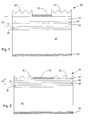
- Figure 1 is a schematic illustration taken in cross section of a diode according to the present invention with the diode broadly designated at 20.
- the diode includes a substrate 21 selected from the group consisting of semiconducting and conducting substrates, a Group III nitride based light emitting layer 22 on or above the substrate 21, and a lenticular surface 23 that contains silicon carbide on or above the light emitting layer 22.
- These Group III nitride layers together define a light emitting region 37.
- the silicon carbide of the lenticular surface 23 is single crystal. It will be understood by those familiar with silicon carbide and crystal structure that the descriptive term "single crystal" refers to the silicon carbide material and is entirely consistent with the lenticular surfaces described herein that obviously include a number of individual structures, each of which is formed of single crystal silicon carbide.
- the substrate can likewise be single crystal silicon carbide, but can also be selected from other materials such as silicon (Si), gallium arsenide (GaAs) or copper-tungsten (Cu-W)
- layers of materials "on" one another can refer to either layers that are above one another (with something in between) and layers that are directly in contact with one another.
- the diode includes respective ohmic contacts 24 to the substrate 21 and 25 to the light emitting region 37 or to the epitaxial layer 27.
- the backside ohmic contact 24 is relatively large for the purpose of encouraging current flow through the diode 20 while the ohmic contact 25 to the light emitting region 37 is typically smaller and in the form of a wire bond pad for minimizing the degree to which the ohmic contact 25 blocks light from leaving the diode.
- Figure 1 also illustrates that in several embodiments, the diode will include both p-type and n-type layers of Group III nitride for current injection across the p-n injunction and encouraging the recombination of carriers in the light emitting layer 22.
- Figure 1 illustrates such layers as an n-type layer 27 and a p-type layer 26. Accordingly, Figure 1 shows three Group III nitride layers (22, 26, 27) but in some embodiments (not illustrated) only one p-type layer and one n-type layer are included.
- the preferred Group III nitride material is aluminum indium gallium nitride (Al x In y Ga 1-x-y N where 0 ⁇ x, y ⁇ 1 and x+y ⁇ 1) and the atomic fractions of aluminum, indium and gallium in each layer are selected so that light emitting layer 22 has a bandgap smaller than either of the adjacent layers 26 or 27.
- the adjustment of the atomic fractions (i.e., x and y) of the Group III elements to obtain the desired bandgap is well understood in this art and can be carried out without undue experimentation.
- other factors are typically considered such as crystal structure, stability, and the desired or necessary manufacturing steps.
- the substrate 21 is formed of single crystal silicon carbide (SiC) and is formed of one of the 3C, 4H, 6H and 15R polytypes of silicon carbide.
- SiC single crystal silicon carbide
- the invention is not limited to these polytypes, they have favorable characteristics of thermal expansion and thermal conductivity.
- the substrate 21 can also be a sub-mounting structure.
- a metal bonding layer 30 can be favorably incorporated, typically for the purpose of manufacturing steps.
- the metal layer 30 preferably includes a metal that forms a higher-temperature bond (e.g. above about 260 °C) which is helpful (or in some cases necessary) for lead-free assembly processes.
- the metal layer 30 uses gold (Au) and tin (Sn) either as a eutectic blend or as individual layers.
- the diode 20 can also include a mirror layer 31 for enhancing the light extraction from the emitting layer 22.
- the mirror and the metal bonding layer can be selected of any appropriate metals provided they are conductive and otherwise consistent (do not interfere) with the structure and function of the remainder of the diode 20 and its elements. If the mirror is made of silver (Ag), additional structural layers of metal may be optionally included to prevent migration of silver into adjacent layers while still taking advantage of its reflective properties.
- barrier layers are typically (but not exclusively) formed of a titanium-tungsten (TiW) alloy, a nitride of the TiW alloy, or as a composite of TiW and platinum (Pt).
- Figure 2 illustrates another embodiment of the diode broadly designated at 28. Many of the elements of Figure 2 are identical to those in Figure 1 and thus they retain the same reference numerals and will not be re-described herein. As Figure 2 particularly indicates, however, the lenticular surface, now designated at 32, extends to, but not beyond, the light emitting region 37.
- the lenticular surface 32 is illustrated as upon the n-type Group III nitride layer 27 rather than directly on the light emitting layer 22.
- the lenticular silicon carbide surface 23 includes at least some non-lenticular silicon carbide between the lenticular features and the remainder of the diode 20.
- the lenticular features are immediately upon the remainder of the diode with no silicon carbide in between.
- the lenticular features 23, 32 can be directly adjacent one another or they can be spaced from one another with non-lenticular portions therebetween.
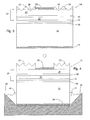
- Figure 3 illustrates yet another embodiment of the diode broadly designated at 34.
- elements common to Figures 1 and 2 carry the same reference numerals.
- the layers that together make up the light emitting region can be broadly considered as a unit which is labeled at 37 in Figure 3 .
- a light emitting layer is designated at 22 while a light emitting region (which includes the emitting layer 22) is designated at 37.
- the light emitting region can be as simple as a p-n junction, or can be formed of a few layers (as illustrated), or of more complex structures such as superlattices and multiple quantum wells.
- the lenticular features are defined both by silicon carbide portions 35 and by features designated at 36 that extend into the remainder of the diode 34.
- the lenticular features 35 and 36 extend into the light emitting region 37, and because in this embodiment the diode 34 includes the n-type epitaxial layer 27, the features 36 extend into such layer 27.
- Figure 4 is another cross-sectional schematic diagram of the diode 20 from Figure 1 positioned on a lead frame 40. Because the diode 20 in Figure 4 is identical to the diode 20 of Figure 1 , all of the elements carry the same reference numerals. It will be further understood that Figure 4 is not drawn to scale, but rather for schematic illustration purposes. As illustrated in Figure 4 , the ohmic contact 24 is positioned between the substrate 21 and the lead frame 40 for providing an appropriate electrical contact between the lead frame 40 and the diode 20. As in many manufacturing techniques for mounting and packaging light emitting diodes, a conductive paste 41 helps attach the diode 20 to the lead frame. As illustrated in Figure 4 and as set forth in co-pending application No. 10/951,042, the substrate is of sufficient thickness to prevent the conductive paste 40 from touching (and thus electrically shorting) the Group III nitride region 37 or the light emitting layer 22.
- Figure 4 illustrates the diode 20 in relatively large proportional context, it preferably incorporates structural advantages to create a total thickness between and including the ohmic contacts 24 and 25 of no more than 150 microns. It will also be understood in this context that the wire bond pad ohmic contact 25 is shown as being positioned lower than the top of the lenticular surface 23. In such cases, the diode 20 would have a thickness no more than 150 microns inclusive of the backside ohmic contact 24 and the lenticular features 23.
- Figures 1 through 4 are schematic rather than limiting of the diodes according to the claimed invention.
- portions of the diodes, often including the light emitting region are formed as mesas rather than with entirely vertical sides illustrated in Figures 1- 4 .
- the illustrated structures or related mesa structures can typically include passivation layers for various well-understood purposes. Because the nature of the invention is such that it can be incorporated with or without mesa structures and with or without supplementary passivation, these alternative structures have not been specifically illustrated, but fall within the scope of the claims.
- Figure 5 shows the invention in the context of a wafer structure.
- the wafer structure can be an extension of the individual diodes that are formed from the wafer.
- Figure 5 illustrates a wafer broadly designated at 43 that includes a substrate 44, preferably (but not necessarily) a single crystal n-type silicon carbide substrate, a light emitting region 37 that can include one or more light emitting layers or combination of layers that together function to emit light when current is injected through them, and a plurality of discrete ohmic contacts 45 that define a plurality of individual diodes broadly designated at 46 and separated by the guidelines 47.
- the wafer includes the lenticular silicon carbide surface features designated at 50 on the Group III nitride active region 37.
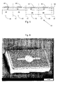
- FIGS. 6 through 10 are scanning electron microscope (SEM) photographs of diodes and portions of diodes according to the present invention.
- Figure 6 is a perspective view of a single light emitting diode according to the present invention. Both the lenticular surface and the top wire bond pad are clearly visible on top of a substrate which is best shown in other of the photographs.
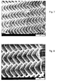
- Figures 7 and 8 illustrate that the lenticular surface can comprise a plurality of cones.
- the features may be more accurately described as cone-like because in a geometry sense, a proper solid cone is generated by rotating a right triangle about one of its legs.
- the slightly rounded shapes of the cones in Figures 7 and 8 are thus slightly different from a solid cone, but the description will be understood by those of skill in the art and in context of the photographs.
- the lenticular surface can be formed of a plurality of pyramids which are likewise defined as a solid figure contained by planes which is constructed from one plane to one point. Both four-sided and six sided pyramids can be incorporated.
- lenticular surfaces can be formed in an almost endless variety depending upon the masking and etching techniques used to form or generate the features.
- the invention is not limited to cones, cone-like features or pyramids, but will encompass other lenticular surfaces that can be selected by those of skill in this art and without undue experimentation.
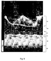
- Figure 9 is a cross-sectional views showing actual examples of some of the features that were illustrated schematically in Figures 1-4 .
- Figure 9 illustrates the lenticular portion at 52 (to differentiate from the schematic diagrams of Figures 1-4 ).
- the additional silicon carbide portion below the lenticular features 52 is designated at 53.
- the light emitting region, including several layers, is designated at 54 and would correspond to region 37 in Figures 3 and 4 .
- the substrate is illustrated at 55.
- the invention offers several advantages.
- the various laser lift-off techniques for reducing the thickness of a substrate are difficult to carry out in a practical sense without inducing cracking of the wafer.
- the substrate removal grinding technique that is compatible with the present invention is expected to give higher yield.
- laser lift-off releases nitrogen gas.
- nitrogen release is a major cracking mechanism in these materials systems.
- the normally disadvantageous absorption in the silicon carbide is effectively minimized because the volume of the lenticular shapes is likewise minimal.
- the absorption coefficient of gallium nitride is generally higher than that of silicon carbide, with the proviso that the absorbency (absorption) of a gallium nitride epitaxial layer cannot be directly compared to a bulk silicon carbide crystal.
- gallium nitride will start to exhibit cracking problems at thicknesses of between about 3 and 4 microns when silicon carbide is used as the substrate and at about 5 microns when sapphire is used as a substrate.
- the use of the more robust SiC for the lenticular features offers structural advantages.
- gallium nitride typically has a defect density in the range of 10 8 to 109 per cubic centimeter (cm-3). In turn, defects can act as undesired absorption centers. In contrast, the typical defect density in silicon carbide is between about 103 and 104 cm -3 . Accordingly, incorporating silicon carbide results in a better quality crystal that demonstrates lower defect absorption, which is advantageous for the efficiency of a light emitting diode.
- silicon carbide gives the greatest latitude for machining or otherwise forming the lenticular surface.
- Silicon carbide also has a higher refractive index than gallium nitride, a factor that has no net disadvantage and may provide additional advantages.
- Figure 9 is a scanning electron microscope photograph taken cross-sectionally of a portion of a diode according to the present invention.
- the various elements of the diode are labeled with the bracketed arrows adjacent the photograph.
- Figure 9 accordingly illustrates the lenticular surface 52, and the non-lenticular portion of silicon carbide 53.
- the light emitting region is again designated at 37, the mirror (and related barrier metals) at 31 and the metal bonding layer at 30.
- a portion of the substrate is labeled 55 at the bottom of the photograph.
- the five micron scale adjacent the photograph gives an indication of the relative sizes of the lenticular features and the relative thicknesses of the layers.
- Figure 10 is a cross-sectional schematic view of another embodiment of the present invention illustrating portions of a diode structure 60 that enhances the amount of light extraction for a given amount of current applied across the diode.
- the reference numerals in Figure 10 are the same as those used in Figures 1 through 4 .
- Figure 10 includes the wire bond pad 25 on the n-type Group III nitride layer 27.
- Figure 10 also illustrates the light emitting layer 22 and the p-type Group III nitride layer 26.
- the lenticular features are again indicated at 23.
- the mirror layer is now designated as 61.
- the mirror layer 61 is no longer a complete layer of the mirror metal (which also forms a portion of the electrical contact to the active region 37). Instead, a portion of the mirror and contact metals have been removed (or simply not included) to define an opening (designated at 62) adjacent the layer 26 beneath the geometric projection of the wire bond pad 25 through the diode 60. Avoiding metal contact at or over a geometric position projected from the wire bond pad 25 helps direct current flow in the more transparent portions of the diode 60 between the mirror (and related metal) layer 61 and the wire bond pad 25.
- the design reduces the number of light-emitting recombinations occurring directly under the wire bond pad 25, and increases the number of recombinations under the more transparent portions of the diode 60. This in turn increases the light extraction from the diode 60 for a given amount of current as compared to a diode in which the mirror and contact system 61 completely covers one side (or the majority of one side) of the diode.
- Figure 11 is a top plan view of the diode 60 taken along lines 11-11 in Figure 10 .
- the layer 26 is again illustrated in the cross-hatched pattern, but the area not included in the mirror (e.g. an opening) is illustrated as the dark circle 62.
- the opening 62 is indicated with the darker shading because it has a darker appearance when the diode is constructed in the embodiment of Figure 10 .
- Figure 12 illustrates another embodiment of the diode designated at 64 in which the opening 62 is filled with a reflective metal 65 but one that does not form an ohmic contact with the layer 26.
- the diode 64 is somewhat better than that of the diode 60 illustrated in Figure 10 because the mirror 61 includes more reflective area while still providing a structure that minimizes the number of recombinations and emitting events occurring directly under the wire bond pad 25.
- Figure 13 shows yet another embodiment of the diode designated at 66 in which a portion 70 of the p-type Group III nitride layer 26 is passivated, preferably using a plasma, to be less conductive or even insulating. Because the passivation portion 70 discourages current flow, a full mirror layer 67 can be included in the diode 66 while still serving to minimize the recombinations taking place directly under the wire bond 25.
- Figures 10-13 illustrate the opening 62, the alternative metal portion 65, and the passivation portion 70 as being identical in size and geometry to the wire bond pad 25, variations in the size of the opening 62, the alternative metal portion 65, or the passivation layer 70 can be carried out for the same purpose without departing from the scope of the claimed invention.
- Figure 14 is another embodiment of a diode broadly designated at 70 according to the present invention.
- the embodiment illustrated at 70 is very similar to the embodiment illustrated in the other figures, with the exception that the light emitting region 37 is in the form of a mesa that in turn includes a passivation layer 71 that covers otherwise exposed portions of the mirror 31 (and any related encapsulating metals) and the bonding metal (or metals) layer 30. Because of the similarity to the other figures, Figure 14 includes identical reference numerals wherever appropriate.
- the passivation layer covers both the walls of the mesa and the silicon carbide lenticular surface 23.
- Appropriate passivation materials included silicon nitride (both stoichiometric Si3N4 and non-stoichiometric) and silicon dioxide (Si02). It will be understood that these or other passivation materials, and the geometry that they cover or include, are selected for functional compatibility with the diode, including relatively high transparency so as not to interfere with the extraction of light from the diode or otherwise reduce its external efficiency.
Abstract
Description
- The present invention relates to light emitting diodes ("LEDs") and in particular relates to high-brightness light emitting diodes formed from Group III nitride active structures on silicon carbide substrates.
- The semiconductor era has witnessed the replacement of many types of electrical devices with solid state counterparts. The most obvious is perhaps the replacement of the vacuum tube (almost unknown to present younger generations) with the transistor. Solid state devices, because of their nature and operation, are inherently much more reliable than earlier generations of electronic devices and can have significantly longer lifetimes, typically by a factor of at least 100. In comparison to such mature technologies, solid-state devices are longer-lasting, physically more rugged, use less power, and are more efficient.
- A light emitting diode (LED) is a p-n junction semiconductor diode that emits light when current is injected across a p-n junction (forward biased) to drive the recombination of electrons and holes with the concurrent production of photons. Thus, light emitting diodes produce light based upon the movement of electrons in a semiconductor material. Therefore, LEDs do not require (although they can be used in conjunction with) vapors or phosphors. They share the desirable characteristics of most semiconductor-based devices, including high efficiency (their emissions comparatively little heat), high reliability and long life. For example, typical LEDs have a mean time between failures of between about 100,000 and 1,000,000 hours meaning that a conservative half lifetime for an LED is on the order of 50,000 hours.
- An LED's emitted light has a frequency (which in turn relates directly to wavelength and color in accordance with well-understood principles of physics) based upon the energy difference between permitted energy levels in the material, a characteristic referred to as the bandgap. The bandgap is a fundamental property of the semiconductor material and its doping. For example, gallium arsenide phosphide (GaAsP) represents a well-established material system for light emitting diodes. Depending on the mole fraction of Ga and As, these materials have a bandgap of between about 1.42 and 1.98 electron volts (eV), and will emit light in the infrared, red and orange portions of the electromagnetic spectrum.
- In order to further commercialize light emitting diode applications, however, colors other than red, orange and yellow must be available. Specifically blue and green light emitting diodes are required (along with red diodes) to create white light or full color displays. Because these colors represent higher-energy portions of the visible spectrum, they require larger transitions than the bandgaps of silicon or gallium arsenide can provide.
- In turn, because green, blue, and ultraviolet (UV) photons represent higher frequency colors (E = hυ) within (and beyond) the visible spectrum, they can only be produced by LEDs with bandgaps of at least about 2.2 eV. Such materials include diamond (5.47 eV), silicon carbide (2.99 eV) and Group III nitrides such as GaN (3.4 eV). In addition to producing green, blue or ultraviolet light per se, wide bandgap LEDs can be combined with red and green LEDs to produce white light, or with phosphors that produce white light when excited by blue or UV light, or both.
- For several reasons, the Group III nitride compositions (i.e., Group III of the periodic table), particularly GaN, AlGaN, InGaN and AlInGaN are particularly useful for LEDs that emit in the ultraviolet (UV) through green portions of the spectrum. As one advantage, they are "direct" bandgap materials, meaning that when an electron transition occurs across the bandgap, much of the energy is emitted as light. By comparison, "indirect" materials (such as silicon carbide) emit their energy partially as light (a photon) and predominantly as vibrational energy (a phonon). Thus Group III nitrides offer efficiency advantages over indirect transition materials.
- As another advantage, the bandgap of ternary and quaternary Group III materials (e.g., AlGaN, InGaN, AlInGaN) depends upon the atomic fraction of the included Group III elements. Thus the wavelength (color) of the emission can be tailored (within limits) by controlling the atomic fraction of each Group III element in a ternary or quaternary nitride.
- Wide bandgap semiconductors have been, however, historically more difficult to produce and work with than gallium-arsenide or gallium phosphide (GaP). As a result, blue and UV-emitting LEDs have lagged behind GaP-based LED's in their commercial appearance. For example, silicon carbide is physically very hard, has no melt phase, and requires high temperatures (on the order of about 1500-2000 °C) for epitaxial or sublimation growth. The Group III nitrides have relatively large nitrogen vapor pressures at their melting temperatures and thus are likewise difficult or impossible to grow from a melt. Additionally, difficulties in obtaining p-type gallium nitride (and other Group III nitrides) remained a barrier to diode production for a number of years. Accordingly, the commercial availability of blue and white-emitting LEDs is more recent than the corresponding availability of GaP-based and GaAs-based LEDs.
- A number of commonly assigned patents and co-pending patent applications likewise discuss the theory and nature of light emitting diodes, including but not limited to
U.S. Patent Nos. 6,459,100 ;6,373,077 ;6,201,262 ;6,187,606 ;5,912,477 ;5,416,342 ; and5,838,706 ; and PublishedU.S. Applications Nos. 20020022290 ;20020093020 ; and20020123164 . - Blue LEDs and their related derivative devices are becoming more frequently included in consumer electronic devices, particularly small displays. Common examples include items such as computer screens, personal digital assistants ("PDAs") and cellular phones. In turn, these small devices drive demand for thinner LEDs with reduced area ("footprint"). Such LEDs, however, must still operate at low forward voltages (Vf) and high light output. To date, however, reducing the size of the Group III nitride devices has tended to increase their forward voltage and reduce their radiant flux.
- In addition to providing blue, green, or white light (as well as emissions in the ultraviolet range), the Group III nitride light emitting diodes have the potential to provide replacement for long-standing illumination technologies such as incandescent and fluorescent lighting. Historically, however, LEDs have lacked brightness comparable to incandescent, fluorescent or vapor-discharge lights and thus these older technologies have continued to occupy the field. Only recently, have white LEDs (or LED-based white-emitting devices) begun to make inroads into commercial lighting applications, with most of these being in smaller applications such as flashlights and related items.
- In commercial embodiments of light emitting diodes (e.g., the XBRIGHT™ diodes offered by the assignee herein; Cree, Inc.; Durham, North Carolina) recent advances have included an inverted device design.
U.S. Patent No. 6,740,906 discusses aspects of this design as doesU.S. Patent Application Publication No. 20020123164 . In this type of design, the Group III active layers are grown (typically epitaxially) on a silicon carbide substrate. Light emitting diodes of this type are then mounted with their epitaxial layers ("epilayers") "down" rather than "up"; i.e., the silicon carbide portions form the display face of the mounted device. In this orientation the epitaxial layers are mounted to and face a circuit or "lead frame" that provides the electrical connection to the diode. The silicon carbide-up orientation increases light extraction from the device as set forth in No.20020123164 - Silicon carbide can also be conductively doped. This provides advantages in comparison to sapphire based Group III nitride diodes. Because sapphire is an insulator, two top wire bonds are typically required to mount a working sapphire-based diode. In comparison, silicon carbide devices can be "vertically" oriented; i.e., with ohmic contacts on opposite ends of the device. Such vertical orientation is directly analogous to diodes formed in other conductive semiconductor materials such as gallium arsenide (GaAs), and thus the same mounting orientations and techniques can be used.
- Although these "inverted" devices have successfully provided significant practical and commercial improvements, their "epilayer-down" orientation requires different, and to some extent more sophisticated, mounting on lead frames. In particular, because the active portion (p-n junction, multiple quantum well, etc.) is positioned closely adjacent to the lead frame, avoiding short circuits or other undesired interactions between the active portion and lead frame becomes more difficult.
- For example, conventional LEDs (including Group III nitride on SiC devices) are often mounted on the lead frame using conductive silver epoxy. Silver epoxy is a mixture of more than about 50 percent by weight of microscopic silver particles with epoxy resin precursors. When used to connect electronic devices to circuits (or circuit boards) the silver epoxy provides flexibility, relative ease of handling, conductivity and good heat transfer properties. Because silver epoxy is (purposely) applied as a viscous liquid, it can and will flow accordingly and, unless other steps are taken, will tend to surround lower portions of any diode mounted with it. As noted above, if the active portions are adjacent the lead frame, the flowing silver epoxy can contact the active portion and cause short circuiting or other undesired interactions.
- As a result, many conventional light emitting diode mounting techniques are either too difficult, too unreliable or simply unavailable for inverted Group III nitride silicon carbide devices. Other specific techniques should or must be incorporated to avoid these problems.
- As another potential solution, the inverted device can be positioned on some sort of sub-structure, with the sub-structure being attached to the lead frame. Examples include
U.S. Patent Application Publication No. 20030213965 . The sub-structure is included to add sufficient thickness to remove the active portions farther from the lead frame and its silver epoxy or related materials. As set forth in No.20030213965 , however, soldering the device to a substructure can undesirably tilt the device with respect to the sub-structure and thereby exacerbate the short-circuiting problem. - Accordingly, it remains a continuing goal to increase the current capacity, light output (power) and light extraction (geometry) capabilities of inverted light emitting diodes while concurrently reducing their size and particularly reducing their thickness. It remains a similar goal to produce such diodes in designs that can be conveniently incorporated into lead frames, packages and circuits in a manner similar or identical to related diodes.
- In one aspect the invention is a high efficiency Group III nitride light emitting diode that includes a substrate selected from the group consisting of semiconducting and conducting materials, a Group III nitride-based light emitting region on the substrate; and a lenticular surface containing single crystal silicon carbide on the light emitting region.
- In another aspect the invention is a high efficiency Group III nitride light emitting diode that includes a conductive silicon carbide substrate; an aluminum indium gallium nitride light emitting region on the substrate, and a thin lenticular surface of silicon carbide on the light emitting region.
- In another aspect, the invention is a high efficiency Group III nitride light emitting diode that includes a substrate selected from the group consisting of conducting and semiconducting materials, at least one metal bonding layer on one surface of the substrate, an ohmic contact to the opposite surface of the substrate from the metal layer, a light emitting structure based upon the Group III nitride system on the at least one metal layer on the substrate, an ohmic contact on the light emitting structure opposite the substrate, and a lenticular surface, at least portions of which are formed of silicon carbide, on the portions of the light emitting structure other than the ohmic contact.
- In another aspect, the invention is a high efficiency Group III nitride light emitting diode that includes a silicon carbide substrate, a backside ohmic contact on one surface of the substrate for providing one electrical connection to the diode, a metal bonding layer on the opposite surface of the substrate for providing a physical and electronic transition between the substrate and other portions of the diode, a mirror layer on the metal bonding layer for enhancing light extraction from the diode, a p-type Group III nitride layer on the mirror, a light emitting Group III nitride layer on the p-type layer and having a bandgap smaller than the bandgap of the p-type layer, an n-type Group III nitride layer on the light emitting layer and having a bandgap larger than the bandgap of the light emitting layer, a wire bond pad ohmic contact to the n-type layer for providing a second electrical connection to the diode, and a lenticular surface, at least portions of which are formed of silicon carbide, on the portions of the n-type layer other than the wire bond pad.
- In another aspect, the invention is a high-efficiency Group III nitride light emitting diode package that includes a lead frame, and a light emitting diode on the lead frame, the diode including, a substrate selected from the group consisting of semiconducting and conducting materials, a Group III nitride based light emitting region on the substrate, a lenticular surface containing single crystal silicon carbide on the light emitting region, an ohmic contact between the substrate and the lead frame, and an ohmic contact to the light emitting region.
- In another aspect, the invention is a wafer structure for high efficiency Group III nitride light emitting diode precursors that includes a conductive silicon carbide substrate wafer, a Group III nitride epitaxial layer on the substrate, a plurality of discrete ohmic contacts on the surface of the Group III nitride epitaxial layer, the ohmic contacts defining a plurality of discrete light emitting diode precursors, and a lenticular surface containing single crystals silicon carbide on the Group III nitride epitaxial layer.
- The foregoing and other objects and advantages of the invention and the manner in which the same are accomplished will become clearer based on the followed detailed description taken in conjunction with the accompanying drawings.
-
Figure 1 is a cross sectional schematic illustration of a diode according to the present invention. -
Figure 2 is a cross sectional schematic illustration of a second embodiment of a diode according to the present invention. -
Figure 3 is a cross-sectional schematic illustration of a third embodiment of a diode according to the present invention. -
Figure 4 is a schematic cross-sectional illustration of a diode and a lead frame in accordance with the present invention. -
Figure 5 is a cross sectional schematic diagram of a semiconductor wafer in accordance with the present invention. -
Figure 6 is a scanning electron microscope (SEM) photograph of a diode according to the present invention. -
Figures 7 and 8 are SEM photographs of the surface of a diode according to the present invention. -
Figures 9 is an SEM photograph taken cross-sectionally across a diode according to the present invention. -
Figure 10 is a schematic cross-sectional view of another embodiment of a diode according to the present invention. -
Figures 11 is a sectional view taken along lines 11-11 ofFigure 10 . -
Figures 12 and 13 are additional cross-sectional views of additional embodiments of diodes according to the present invention. -
Figure 14 is a cross-sectional view of a diode with a mesa structure according to the present invention. - In a first aspect, the invention is a high efficiency Group III nitride light emitting diode.
Figure 1 is a schematic illustration taken in cross section of a diode according to the present invention with the diode broadly designated at 20. The diode includes asubstrate 21 selected from the group consisting of semiconducting and conducting substrates, a Group III nitride basedlight emitting layer 22 on or above thesubstrate 21, and alenticular surface 23 that contains silicon carbide on or above thelight emitting layer 22. These Group III nitride layers together define alight emitting region 37. - In most embodiments, the silicon carbide of the
lenticular surface 23 is single crystal. It will be understood by those familiar with silicon carbide and crystal structure that the descriptive term "single crystal" refers to the silicon carbide material and is entirely consistent with the lenticular surfaces described herein that obviously include a number of individual structures, each of which is formed of single crystal silicon carbide. The substrate can likewise be single crystal silicon carbide, but can also be selected from other materials such as silicon (Si), gallium arsenide (GaAs) or copper-tungsten (Cu-W) - As used in the context of the invention, the description of layers of materials "on" one another can refer to either layers that are above one another (with something in between) and layers that are directly in contact with one another. Each meaning will be clear in context, particularly to those persons of ordinary skill in this art.
- As further illustrated in
Figure 1 , the diode includes respectiveohmic contacts 24 to thesubstrate light emitting region 37 or to theepitaxial layer 27. As is typical in many diodes of this type, the backsideohmic contact 24 is relatively large for the purpose of encouraging current flow through thediode 20 while theohmic contact 25 to thelight emitting region 37 is typically smaller and in the form of a wire bond pad for minimizing the degree to which theohmic contact 25 blocks light from leaving the diode. -
Figure 1 also illustrates that in several embodiments, the diode will include both p-type and n-type layers of Group III nitride for current injection across the p-n injunction and encouraging the recombination of carriers in thelight emitting layer 22.Figure 1 illustrates such layers as an n-type layer 27 and a p-type layer 26. Accordingly,Figure 1 shows three Group III nitride layers (22, 26, 27) but in some embodiments (not illustrated) only one p-type layer and one n-type layer are included. - Thus, in embodiments for which
Figure 1 is illustrative, the preferred Group III nitride material is aluminum indium gallium nitride (AlxInyGa1-x-yN where 0 ≤ x, y ≤ 1 and x+y ≤ 1) and the atomic fractions of aluminum, indium and gallium in each layer are selected so that light emittinglayer 22 has a bandgap smaller than either of theadjacent layers - The adjustment of the atomic fractions (i.e., x and y) of the Group III elements to obtain the desired bandgap is well understood in this art and can be carried out without undue experimentation. In addition to selecting the atomic fractions on the basis of the desired bandgap, other factors are typically considered such as crystal structure, stability, and the desired or necessary manufacturing steps.
- In preferred embodiments, the
substrate 21 is formed of single crystal silicon carbide (SiC) and is formed of one of the 3C, 4H, 6H and 15R polytypes of silicon carbide. Although the invention is not limited to these polytypes, they have favorable characteristics of thermal expansion and thermal conductivity. - The
substrate 21 can also be a sub-mounting structure. In either case (silicon carbide substrate or sub-mounting structure substrate), ametal bonding layer 30 can be favorably incorporated, typically for the purpose of manufacturing steps. Themetal layer 30 preferably includes a metal that forms a higher-temperature bond (e.g. above about 260 °C) which is helpful (or in some cases necessary) for lead-free assembly processes. In presently preferred embodiments themetal layer 30 uses gold (Au) and tin (Sn) either as a eutectic blend or as individual layers. - The
diode 20 can also include amirror layer 31 for enhancing the light extraction from the emittinglayer 22. The mirror and the metal bonding layer can be selected of any appropriate metals provided they are conductive and otherwise consistent (do not interfere) with the structure and function of the remainder of thediode 20 and its elements. If the mirror is made of silver (Ag), additional structural layers of metal may be optionally included to prevent migration of silver into adjacent layers while still taking advantage of its reflective properties. Such barrier layers are typically (but not exclusively) formed of a titanium-tungsten (TiW) alloy, a nitride of the TiW alloy, or as a composite of TiW and platinum (Pt). -
Figure 2 illustrates another embodiment of the diode broadly designated at 28. Many of the elements ofFigure 2 are identical to those inFigure 1 and thus they retain the same reference numerals and will not be re-described herein. AsFigure 2 particularly indicates, however, the lenticular surface, now designated at 32, extends to, but not beyond, thelight emitting region 37. - Thus, in
Figure 2 thelenticular surface 32 is illustrated as upon the n-type GroupIII nitride layer 27 rather than directly on thelight emitting layer 22. Stated differently, inFigure 1 the lenticularsilicon carbide surface 23 includes at least some non-lenticular silicon carbide between the lenticular features and the remainder of thediode 20. InFigure 2 , the lenticular features are immediately upon the remainder of the diode with no silicon carbide in between. In either embodiment (Figure 1 or Figure 2 ) the lenticular features 23, 32 can be directly adjacent one another or they can be spaced from one another with non-lenticular portions therebetween. -
Figure 3 illustrates yet another embodiment of the diode broadly designated at 34. Once again, elements common toFigures 1 and 2 carry the same reference numerals. As a further explanation and illustration, in all of the embodiments, the layers that together make up the light emitting region, regardless of the number of layers, can be broadly considered as a unit which is labeled at 37 inFigure 3 . Thus, inFigures 1-4 herein, a light emitting layer is designated at 22 while a light emitting region (which includes the emitting layer 22) is designated at 37. Those familiar with light emitting structures will recognize that the light emitting region can be as simple as a p-n junction, or can be formed of a few layers (as illustrated), or of more complex structures such as superlattices and multiple quantum wells. - In
Figure 3 , however, the lenticular features are defined both bysilicon carbide portions 35 and by features designated at 36 that extend into the remainder of thediode 34. In particular, in the embodiment illustrated inFigure 3 the lenticular features 35 and 36 extend into thelight emitting region 37, and because in this embodiment thediode 34 includes the n-type epitaxial layer 27, thefeatures 36 extend intosuch layer 27. -
Figure 4 is another cross-sectional schematic diagram of thediode 20 fromFigure 1 positioned on alead frame 40. Because thediode 20 inFigure 4 is identical to thediode 20 ofFigure 1 , all of the elements carry the same reference numerals. It will be further understood thatFigure 4 is not drawn to scale, but rather for schematic illustration purposes. As illustrated inFigure 4 , theohmic contact 24 is positioned between thesubstrate 21 and thelead frame 40 for providing an appropriate electrical contact between thelead frame 40 and thediode 20. As in many manufacturing techniques for mounting and packaging light emitting diodes, aconductive paste 41 helps attach thediode 20 to the lead frame. As illustrated inFigure 4 and as set forth in co-pending application No. 10/951,042, the substrate is of sufficient thickness to prevent theconductive paste 40 from touching (and thus electrically shorting) the GroupIII nitride region 37 or thelight emitting layer 22. - Furthermore, although
Figure 4 illustrates thediode 20 in relatively large proportional context, it preferably incorporates structural advantages to create a total thickness between and including theohmic contacts ohmic contact 25 is shown as being positioned lower than the top of thelenticular surface 23. In such cases, thediode 20 would have a thickness no more than 150 microns inclusive of the backsideohmic contact 24 and the lenticular features 23. - It will be understood that
Figures 1 through 4 are schematic rather than limiting of the diodes according to the claimed invention. For example, those familiar with diodes of this type will recognize that portions of the diodes, often including the light emitting region, are formed as mesas rather than with entirely vertical sides illustrated inFigures 1- 4 . Additionally, the illustrated structures or related mesa structures can typically include passivation layers for various well-understood purposes. Because the nature of the invention is such that it can be incorporated with or without mesa structures and with or without supplementary passivation, these alternative structures have not been specifically illustrated, but fall within the scope of the claims. -
Figure 5 shows the invention in the context of a wafer structure. In one sense, the wafer structure can be an extension of the individual diodes that are formed from the wafer. Thus,Figure 5 illustrates a wafer broadly designated at 43 that includes asubstrate 44, preferably (but not necessarily) a single crystal n-type silicon carbide substrate, alight emitting region 37 that can include one or more light emitting layers or combination of layers that together function to emit light when current is injected through them, and a plurality of discreteohmic contacts 45 that define a plurality of individual diodes broadly designated at 46 and separated by theguidelines 47. The wafer includes the lenticular silicon carbide surface features designated at 50 on the Group III nitrideactive region 37. -
Figures 6 through 10 are scanning electron microscope (SEM) photographs of diodes and portions of diodes according to the present invention. -
Figure 6 is a perspective view of a single light emitting diode according to the present invention. Both the lenticular surface and the top wire bond pad are clearly visible on top of a substrate which is best shown in other of the photographs. -
Figures 7 and 8 illustrate that the lenticular surface can comprise a plurality of cones. The features may be more accurately described as cone-like because in a geometry sense, a proper solid cone is generated by rotating a right triangle about one of its legs. The slightly rounded shapes of the cones inFigures 7 and 8 are thus slightly different from a solid cone, but the description will be understood by those of skill in the art and in context of the photographs. In other embodiments, the lenticular surface can be formed of a plurality of pyramids which are likewise defined as a solid figure contained by planes which is constructed from one plane to one point. Both four-sided and six sided pyramids can be incorporated. - Other shapes for lenticular surfaces can be formed in an almost endless variety depending upon the masking and etching techniques used to form or generate the features. Thus, the invention is not limited to cones, cone-like features or pyramids, but will encompass other lenticular surfaces that can be selected by those of skill in this art and without undue experimentation.
-
Figure 9 is a cross-sectional views showing actual examples of some of the features that were illustrated schematically inFigures 1-4 . -
Figure 9 illustrates the lenticular portion at 52 (to differentiate from the schematic diagrams ofFigures 1-4 ). The additional silicon carbide portion below the lenticular features 52 is designated at 53. The light emitting region, including several layers, is designated at 54 and would correspond toregion 37 inFigures 3 and 4 . The substrate is illustrated at 55. - In comparison to other techniques and structures, the invention offers several advantages. For example, the various laser lift-off techniques for reducing the thickness of a substrate (and thus of the resulting diode; e.g., Published Patent Application No.
20030197170 - As another benefit, the normally disadvantageous absorption in the silicon carbide is effectively minimized because the volume of the lenticular shapes is likewise minimal.
- As another advantage, the absorption coefficient of gallium nitride is generally higher than that of silicon carbide, with the proviso that the absorbency (absorption) of a gallium nitride epitaxial layer cannot be directly compared to a bulk silicon carbide crystal.
- As another advantage, gallium nitride will start to exhibit cracking problems at thicknesses of between about 3 and 4 microns when silicon carbide is used as the substrate and at about 5 microns when sapphire is used as a substrate. Thus, the use of the more robust SiC for the lenticular features offers structural advantages.
- As another advantage, gallium nitride typically has a defect density in the range of 108 to 109 per cubic centimeter (cm-3). In turn, defects can act as undesired absorption centers. In contrast, the typical defect density in silicon carbide is between about 103 and 104 cm-3. Accordingly, incorporating silicon carbide results in a better quality crystal that demonstrates lower defect absorption, which is advantageous for the efficiency of a light emitting diode.
- As another advantage, for a given thickness of n-type gallium nitride, the presence of silicon carbide always improves the current spreading. Additionally, silicon carbide gives the greatest latitude for machining or otherwise forming the lenticular surface.
- Silicon carbide also has a higher refractive index than gallium nitride, a factor that has no net disadvantage and may provide additional advantages.
-
Figure 9 is a scanning electron microscope photograph taken cross-sectionally of a portion of a diode according to the present invention. The various elements of the diode are labeled with the bracketed arrows adjacent the photograph.Figure 9 accordingly illustrates thelenticular surface 52, and the non-lenticular portion ofsilicon carbide 53. The light emitting region is again designated at 37, the mirror (and related barrier metals) at 31 and the metal bonding layer at 30. A portion of the substrate is labeled 55 at the bottom of the photograph. The five micron scale adjacent the photograph gives an indication of the relative sizes of the lenticular features and the relative thicknesses of the layers. -
Figure 10 is a cross-sectional schematic view of another embodiment of the present invention illustrating portions of adiode structure 60 that enhances the amount of light extraction for a given amount of current applied across the diode. Where possible and helpful, the reference numerals inFigure 10 are the same as those used inFigures 1 through 4 . Thus,Figure 10 includes thewire bond pad 25 on the n-type GroupIII nitride layer 27.Figure 10 also illustrates thelight emitting layer 22 and the p-type GroupIII nitride layer 26. The lenticular features are again indicated at 23. - The mirror layer, however, is now designated as 61. In the embodiment illustrated in
Figure 10 , themirror layer 61 is no longer a complete layer of the mirror metal (which also forms a portion of the electrical contact to the active region 37). Instead, a portion of the mirror and contact metals have been removed (or simply not included) to define an opening (designated at 62) adjacent thelayer 26 beneath the geometric projection of thewire bond pad 25 through thediode 60. Avoiding metal contact at or over a geometric position projected from thewire bond pad 25 helps direct current flow in the more transparent portions of thediode 60 between the mirror (and related metal)layer 61 and thewire bond pad 25. By eliminating a portion of themirror 61, the design reduces the number of light-emitting recombinations occurring directly under thewire bond pad 25, and increases the number of recombinations under the more transparent portions of thediode 60. This in turn increases the light extraction from thediode 60 for a given amount of current as compared to a diode in which the mirror andcontact system 61 completely covers one side (or the majority of one side) of the diode. -
Figure 11 is a top plan view of thediode 60 taken along lines 11-11 inFigure 10 . Thelayer 26 is again illustrated in the cross-hatched pattern, but the area not included in the mirror (e.g. an opening) is illustrated as thedark circle 62. Theopening 62 is indicated with the darker shading because it has a darker appearance when the diode is constructed in the embodiment ofFigure 10 . -
Figure 12 illustrates another embodiment of the diode designated at 64 in which theopening 62 is filled with areflective metal 65 but one that does not form an ohmic contact with thelayer 26. As a result, light extraction from thediode 64 is somewhat better than that of thediode 60 illustrated inFigure 10 because themirror 61 includes more reflective area while still providing a structure that minimizes the number of recombinations and emitting events occurring directly under thewire bond pad 25. -
Figure 13 shows yet another embodiment of the diode designated at 66 in which aportion 70 of the p-type GroupIII nitride layer 26 is passivated, preferably using a plasma, to be less conductive or even insulating. Because thepassivation portion 70 discourages current flow, afull mirror layer 67 can be included in thediode 66 while still serving to minimize the recombinations taking place directly under thewire bond 25. - It will be understood that although
Figures 10-13 illustrate theopening 62, thealternative metal portion 65, and thepassivation portion 70 as being identical in size and geometry to thewire bond pad 25, variations in the size of theopening 62, thealternative metal portion 65, or thepassivation layer 70 can be carried out for the same purpose without departing from the scope of the claimed invention. -
Figure 14 is another embodiment of a diode broadly designated at 70 according to the present invention. The embodiment illustrated at 70 is very similar to the embodiment illustrated in the other figures, with the exception that thelight emitting region 37 is in the form of a mesa that in turn includes apassivation layer 71 that covers otherwise exposed portions of the mirror 31 (and any related encapsulating metals) and the bonding metal (or metals)layer 30. Because of the similarity to the other figures,Figure 14 includes identical reference numerals wherever appropriate. In typical embodiments, the passivation layer covers both the walls of the mesa and the silicon carbidelenticular surface 23. Appropriate passivation materials included silicon nitride (both stoichiometric Si3N4 and non-stoichiometric) and silicon dioxide (Si02). It will be understood that these or other passivation materials, and the geometry that they cover or include, are selected for functional compatibility with the diode, including relatively high transparency so as not to interfere with the extraction of light from the diode or otherwise reduce its external efficiency. - In the drawings and specification there has been set forth a preferred embodiment of the invention, and although specific terms have been employed, they are used in a generic and descriptive sense only and not for purposes of limitation, the scope of the invention being defined in the claims.
Claims (10)
- A high efficiency Group-III nitride light emitting diode (LED), comprising:a gallium nitride (GaN) based emitting region; anda lenticular features extending into the GaN based emitting region..
- The LED of claim 1, wherein said lenticular features further comprise single crystal silicon carbide.
- The LED of claim 1, wherein said lenticular features comprise a plurality of cones.
- The LED of claim 1, wherein said lenticular features comprise a plurality of pyramids.
- The LED of claim 1, further comprising a phosphor-containing structure adjacent said lenticular surface for converting at least some of the light emitted from said GaN based emitting region.
- The LED of claim 5, emitting white light.
- The LED of claim 1, wherein said GaN based emitting region comprises at least one p-type layer and at least one n-type layer for current injection and recombination in said emitting region.
- The LED of claim 1, wherein said lenticular features are formed on top surface of said emitting region.
- The LED of claim 1, wherein said lenticular features are formed on at least one of the side surfaces of said emitting region.
- The LED of claim 1, wherein said lenticular feature comprise a lenticular surface.
Applications Claiming Priority (3)
| Application Number | Priority Date | Filing Date | Title |
|---|---|---|---|
| US10/951,042 US7259402B2 (en) | 2004-09-22 | 2004-09-22 | High efficiency group III nitride-silicon carbide light emitting diode |
| US11/082,470 US8174037B2 (en) | 2004-09-22 | 2005-03-17 | High efficiency group III nitride LED with lenticular surface |
| EP05797533.6A EP1792350B1 (en) | 2004-09-22 | 2005-09-15 | High efficiency group iii nitride led with lenticular surface |
Related Parent Applications (2)
| Application Number | Title | Priority Date | Filing Date |
|---|---|---|---|
| EP05797533.6 Division | 2005-09-15 | ||
| EP05797533.6A Division-Into EP1792350B1 (en) | 2004-09-22 | 2005-09-15 | High efficiency group iii nitride led with lenticular surface |
Publications (2)
| Publication Number | Publication Date |
|---|---|
| EP2267802A2 true EP2267802A2 (en) | 2010-12-29 |
| EP2267802A3 EP2267802A3 (en) | 2012-07-04 |
Family
ID=35520716
Family Applications (3)
| Application Number | Title | Priority Date | Filing Date |
|---|---|---|---|
| EP10185888.4A Active EP2270878B1 (en) | 2004-09-22 | 2005-09-15 | LED with a lenticular surface |
| EP05797533.6A Active EP1792350B1 (en) | 2004-09-22 | 2005-09-15 | High efficiency group iii nitride led with lenticular surface |
| EP10185898A Withdrawn EP2267802A3 (en) | 2004-09-22 | 2005-09-15 | High efficiency group III nitride LED with lenticular surface |
Family Applications Before (2)
| Application Number | Title | Priority Date | Filing Date |
|---|---|---|---|
| EP10185888.4A Active EP2270878B1 (en) | 2004-09-22 | 2005-09-15 | LED with a lenticular surface |
| EP05797533.6A Active EP1792350B1 (en) | 2004-09-22 | 2005-09-15 | High efficiency group iii nitride led with lenticular surface |
Country Status (6)
| Country | Link |
|---|---|
| US (5) | US8174037B2 (en) |
| EP (3) | EP2270878B1 (en) |
| JP (2) | JP2008514028A (en) |
| KR (3) | KR20100134808A (en) |
| TW (1) | TW200623464A (en) |
| WO (1) | WO2006036565A2 (en) |
Families Citing this family (101)
| Publication number | Priority date | Publication date | Assignee | Title |
|---|---|---|---|---|
| EP2270887B1 (en) | 2003-04-30 | 2020-01-22 | Cree, Inc. | High powered light emitter packages with compact optics |
| US7005679B2 (en) | 2003-05-01 | 2006-02-28 | Cree, Inc. | Multiple component solid state white light |
| US7915085B2 (en) | 2003-09-18 | 2011-03-29 | Cree, Inc. | Molded chip fabrication method |
| US7795623B2 (en) | 2004-06-30 | 2010-09-14 | Cree, Inc. | Light emitting devices having current reducing structures and methods of forming light emitting devices having current reducing structures |
| US7534633B2 (en) | 2004-07-02 | 2009-05-19 | Cree, Inc. | LED with substrate modifications for enhanced light extraction and method of making same |
| US7737459B2 (en) * | 2004-09-22 | 2010-06-15 | Cree, Inc. | High output group III nitride light emitting diodes |
| US8174037B2 (en) | 2004-09-22 | 2012-05-08 | Cree, Inc. | High efficiency group III nitride LED with lenticular surface |
| US7335920B2 (en) | 2005-01-24 | 2008-02-26 | Cree, Inc. | LED with current confinement structure and surface roughening |
| US8729580B2 (en) * | 2005-12-06 | 2014-05-20 | Toshiba Techno Center, Inc. | Light emitter with metal-oxide coating |
| US7614759B2 (en) | 2005-12-22 | 2009-11-10 | Cree Led Lighting Solutions, Inc. | Lighting device |
| US8101961B2 (en) * | 2006-01-25 | 2012-01-24 | Cree, Inc. | Transparent ohmic contacts on light emitting diodes with growth substrates |
| KR100735488B1 (en) * | 2006-02-03 | 2007-07-04 | 삼성전기주식회사 | Method for forming the gan type led device |
| JP2009534866A (en) | 2006-04-24 | 2009-09-24 | クリー, インコーポレイティッド | Horizontally mounted white LED |
| AU2007249229B2 (en) * | 2006-05-12 | 2013-05-23 | Cardinal Health 529, Llc | Balloon expandable bioabsorbable drug eluting flexible stent |
| US8643195B2 (en) | 2006-06-30 | 2014-02-04 | Cree, Inc. | Nickel tin bonding system for semiconductor wafers and devices |
| US7910945B2 (en) * | 2006-06-30 | 2011-03-22 | Cree, Inc. | Nickel tin bonding system with barrier layer for semiconductor wafers and devices |
| US7910938B2 (en) * | 2006-09-01 | 2011-03-22 | Cree, Inc. | Encapsulant profile for light emitting diodes |
| US8425271B2 (en) | 2006-09-01 | 2013-04-23 | Cree, Inc. | Phosphor position in light emitting diodes |
| US7855459B2 (en) | 2006-09-22 | 2010-12-21 | Cree, Inc. | Modified gold-tin system with increased melting temperature for wafer bonding |
| US9178121B2 (en) * | 2006-12-15 | 2015-11-03 | Cree, Inc. | Reflective mounting substrates for light emitting diodes |
| US9159888B2 (en) * | 2007-01-22 | 2015-10-13 | Cree, Inc. | Wafer level phosphor coating method and devices fabricated utilizing method |
| US9024349B2 (en) | 2007-01-22 | 2015-05-05 | Cree, Inc. | Wafer level phosphor coating method and devices fabricated utilizing method |
| US8212262B2 (en) * | 2007-02-09 | 2012-07-03 | Cree, Inc. | Transparent LED chip |
| US20080197378A1 (en) * | 2007-02-20 | 2008-08-21 | Hua-Shuang Kong | Group III Nitride Diodes on Low Index Carrier Substrates |
| US9484499B2 (en) * | 2007-04-20 | 2016-11-01 | Cree, Inc. | Transparent ohmic contacts on light emitting diodes with carrier substrates |
| US9401461B2 (en) | 2007-07-11 | 2016-07-26 | Cree, Inc. | LED chip design for white conversion |
| US9461201B2 (en) | 2007-11-14 | 2016-10-04 | Cree, Inc. | Light emitting diode dielectric mirror |
| US7915629B2 (en) | 2008-12-08 | 2011-03-29 | Cree, Inc. | Composite high reflectivity layer |
| US8536584B2 (en) | 2007-11-14 | 2013-09-17 | Cree, Inc. | High voltage wire bond free LEDS |
| US8575633B2 (en) | 2008-12-08 | 2013-11-05 | Cree, Inc. | Light emitting diode with improved light extraction |
| US20090218588A1 (en) * | 2007-12-06 | 2009-09-03 | Paul Panaccione | Chip-scale packaged light-emitting devices |
| US9041285B2 (en) | 2007-12-14 | 2015-05-26 | Cree, Inc. | Phosphor distribution in LED lamps using centrifugal force |
| US9431589B2 (en) | 2007-12-14 | 2016-08-30 | Cree, Inc. | Textured encapsulant surface in LED packages |
| US8878219B2 (en) * | 2008-01-11 | 2014-11-04 | Cree, Inc. | Flip-chip phosphor coating method and devices fabricated utilizing method |
| US8877524B2 (en) | 2008-03-31 | 2014-11-04 | Cree, Inc. | Emission tuning methods and devices fabricated utilizing methods |
| KR101449030B1 (en) * | 2008-04-05 | 2014-10-08 | 엘지이노텍 주식회사 | group 3 nitride-based semiconductor light emitting diodes and methods to fabricate them |
| CN102047454B (en) * | 2008-04-16 | 2013-04-10 | Lg伊诺特有限公司 | Light-emitting device and fabricating method thereof |
| KR101534846B1 (en) * | 2008-04-16 | 2015-07-07 | 엘지이노텍 주식회사 | fabrication of vertical structured light emitting diodes using group 3 nitride-based semiconductors and its related methods |
| KR101550913B1 (en) * | 2008-05-04 | 2015-09-07 | 엘지이노텍 주식회사 | 3 fabrication of vertical structured light emitting diodes using group 3 nitride-based semiconductors and its related methods |
| US9287469B2 (en) | 2008-05-02 | 2016-03-15 | Cree, Inc. | Encapsulation for phosphor-converted white light emitting diode |
| US20100038670A1 (en) * | 2008-08-18 | 2010-02-18 | Luminus Devices, Inc. | Illumination assembly including chip-scale packaged light-emitting device |
| EP2332185A2 (en) * | 2008-09-08 | 2011-06-15 | 3M Innovative Properties Company | Electrically pixelated luminescent device |
| JP2010067890A (en) * | 2008-09-12 | 2010-03-25 | Hitachi Cable Ltd | Light-emitting element |
| TWI389347B (en) * | 2008-11-13 | 2013-03-11 | Epistar Corp | Opto-electronic device structure and the manufacturing method thereof |
| WO2010056596A2 (en) * | 2008-11-13 | 2010-05-20 | 3M Innovative Properties Company | Electrically pixelated luminescent device incorporating optical elements |
| US8017963B2 (en) * | 2008-12-08 | 2011-09-13 | Cree, Inc. | Light emitting diode with a dielectric mirror having a lateral configuration |
| US8529102B2 (en) * | 2009-04-06 | 2013-09-10 | Cree, Inc. | Reflector system for lighting device |
| US8476668B2 (en) | 2009-04-06 | 2013-07-02 | Cree, Inc. | High voltage low current surface emitting LED |
| US9093293B2 (en) | 2009-04-06 | 2015-07-28 | Cree, Inc. | High voltage low current surface emitting light emitting diode |
| US20100327300A1 (en) | 2009-06-25 | 2010-12-30 | Koninklijke Philips Electronics N.V. | Contact for a semiconductor light emitting device |
| DE102009033686A1 (en) * | 2009-07-17 | 2011-01-20 | Osram Opto Semiconductors Gmbh | Optoelectronic semiconductor component and method for producing an inorganic optoelectronic semiconductor component |
| US8076682B2 (en) * | 2009-07-21 | 2011-12-13 | Koninklijke Philips Electronics N.V. | Contact for a semiconductor light emitting device |
| US9362459B2 (en) * | 2009-09-02 | 2016-06-07 | United States Department Of Energy | High reflectivity mirrors and method for making same |
| US9435493B2 (en) | 2009-10-27 | 2016-09-06 | Cree, Inc. | Hybrid reflector system for lighting device |
| US8981397B2 (en) * | 2010-02-12 | 2015-03-17 | Tsmc Solid State Lighting Ltd. | Light-emitting devices on textured substrates |
| KR101064049B1 (en) * | 2010-02-18 | 2011-09-08 | 엘지이노텍 주식회사 | Semiconductor light emitting device and manufacturing method thereof, light emitting device package |
| US8299479B2 (en) | 2010-03-09 | 2012-10-30 | Tsmc Solid State Lighting Ltd. | Light-emitting devices with textured active layer |
| US9105824B2 (en) | 2010-04-09 | 2015-08-11 | Cree, Inc. | High reflective board or substrate for LEDs |
| US9012938B2 (en) | 2010-04-09 | 2015-04-21 | Cree, Inc. | High reflective substrate of light emitting devices with improved light output |
| WO2011132748A1 (en) * | 2010-04-21 | 2011-10-27 | 京セラ株式会社 | Solar cell module |
| KR101055779B1 (en) * | 2010-06-15 | 2011-08-11 | 서울옵토디바이스주식회사 | Method of fabricating high efficiency light emitting diode |
| KR101735670B1 (en) * | 2010-07-13 | 2017-05-15 | 엘지이노텍 주식회사 | A light emitting device |
| US8476659B2 (en) * | 2010-07-15 | 2013-07-02 | Tsmc Solid State Lighting Ltd. | Light emitting device |
| US10546846B2 (en) | 2010-07-23 | 2020-01-28 | Cree, Inc. | Light transmission control for masking appearance of solid state light sources |
| US8283652B2 (en) * | 2010-07-28 | 2012-10-09 | SemiLEDs Optoelectronics Co., Ltd. | Vertical light emitting diode (VLED) die having electrode frame and method of fabrication |
| US8723160B2 (en) | 2010-07-28 | 2014-05-13 | SemiLEDs Optoelectronics Co., Ltd. | Light emitting diode (LED) die having peripheral electrode frame and method of fabrication |
| US8764224B2 (en) | 2010-08-12 | 2014-07-01 | Cree, Inc. | Luminaire with distributed LED sources |
| KR101795053B1 (en) * | 2010-08-26 | 2017-11-07 | 엘지이노텍 주식회사 | Light emitting device, light emitting device package, light unit |
| US8455882B2 (en) | 2010-10-15 | 2013-06-04 | Cree, Inc. | High efficiency LEDs |
| US8556469B2 (en) | 2010-12-06 | 2013-10-15 | Cree, Inc. | High efficiency total internal reflection optic for solid state lighting luminaires |
| US9166126B2 (en) | 2011-01-31 | 2015-10-20 | Cree, Inc. | Conformally coated light emitting devices and methods for providing the same |
| US8680556B2 (en) | 2011-03-24 | 2014-03-25 | Cree, Inc. | Composite high reflectivity layer |
| US9728676B2 (en) | 2011-06-24 | 2017-08-08 | Cree, Inc. | High voltage monolithic LED chip |
| US10243121B2 (en) | 2011-06-24 | 2019-03-26 | Cree, Inc. | High voltage monolithic LED chip with improved reliability |
| US8686429B2 (en) * | 2011-06-24 | 2014-04-01 | Cree, Inc. | LED structure with enhanced mirror reflectivity |
| US8558252B2 (en) | 2011-08-26 | 2013-10-15 | Cree, Inc. | White LEDs with emission wavelength correction |
| US8573469B2 (en) | 2011-11-18 | 2013-11-05 | LuxVue Technology Corporation | Method of forming a micro LED structure and array of micro LED structures with an electrically insulating layer |
| US8426227B1 (en) * | 2011-11-18 | 2013-04-23 | LuxVue Technology Corporation | Method of forming a micro light emitting diode array |
| US8349116B1 (en) | 2011-11-18 | 2013-01-08 | LuxVue Technology Corporation | Micro device transfer head heater assembly and method of transferring a micro device |
| US8333860B1 (en) | 2011-11-18 | 2012-12-18 | LuxVue Technology Corporation | Method of transferring a micro device |
| US9548332B2 (en) | 2012-04-27 | 2017-01-17 | Apple Inc. | Method of forming a micro LED device with self-aligned metallization stack |
| KR101471351B1 (en) * | 2012-12-27 | 2014-12-10 | 전자부품연구원 | Structure and Fabrication Method of Hybrid Vertical GaN Diode |
| CN104241262B (en) | 2013-06-14 | 2020-11-06 | 惠州科锐半导体照明有限公司 | Light emitting device and display device |
| CN104377287B (en) * | 2013-08-14 | 2017-04-26 | 展晶科技(深圳)有限公司 | Light-emitting diode and manufacturing method thereof |
| US9318475B2 (en) | 2014-05-15 | 2016-04-19 | LuxVue Technology Corporation | Flexible display and method of formation with sacrificial release layer |
| KR102199995B1 (en) * | 2014-06-02 | 2021-01-11 | 엘지이노텍 주식회사 | Light emitting device |
| US9741286B2 (en) | 2014-06-03 | 2017-08-22 | Apple Inc. | Interactive display panel with emitting and sensing diodes |
| US9624100B2 (en) | 2014-06-12 | 2017-04-18 | Apple Inc. | Micro pick up array pivot mount with integrated strain sensing elements |
| US9425151B2 (en) | 2014-06-17 | 2016-08-23 | Apple Inc. | Compliant electrostatic transfer head with spring support layer |
| US9570002B2 (en) | 2014-06-17 | 2017-02-14 | Apple Inc. | Interactive display panel with IR diodes |
| US9705432B2 (en) | 2014-09-30 | 2017-07-11 | Apple Inc. | Micro pick up array pivot mount design for strain amplification |
| US9828244B2 (en) | 2014-09-30 | 2017-11-28 | Apple Inc. | Compliant electrostatic transfer head with defined cavity |
| US9478583B2 (en) | 2014-12-08 | 2016-10-25 | Apple Inc. | Wearable display having an array of LEDs on a conformable silicon substrate |
| US10658546B2 (en) | 2015-01-21 | 2020-05-19 | Cree, Inc. | High efficiency LEDs and methods of manufacturing |
| JP2017034218A (en) * | 2015-08-03 | 2017-02-09 | 株式会社東芝 | Semiconductor light-emitting device |
| TWI552385B (en) * | 2015-09-04 | 2016-10-01 | 錼創科技股份有限公司 | Light emitting device |
| US10170455B2 (en) | 2015-09-04 | 2019-01-01 | PlayNitride Inc. | Light emitting device with buffer pads |
| TWI581460B (en) * | 2015-09-04 | 2017-05-01 | 錼創科技股份有限公司 | Light emitting device and manufacturing method thereof |
| WO2017184686A1 (en) * | 2016-04-19 | 2017-10-26 | The Penn State Research Foundation | Gap-free microdisplay based on iii-nitride led arrays |
| JP6834424B2 (en) * | 2016-12-02 | 2021-02-24 | 日亜化学工業株式会社 | Semiconductor devices and their manufacturing methods |
| EP4082048A4 (en) * | 2019-12-24 | 2024-02-28 | Univ Michigan Regents | Group iii-nitride excitonic heterostructures |
Citations (11)
| Publication number | Priority date | Publication date | Assignee | Title |
|---|---|---|---|---|
| US5416342A (en) | 1993-06-23 | 1995-05-16 | Cree Research, Inc. | Blue light-emitting diode with high external quantum efficiency |
| US5838706A (en) | 1994-09-20 | 1998-11-17 | Cree Research, Inc. | Low-strain laser structures with group III nitride active layers |
| US5912477A (en) | 1994-10-07 | 1999-06-15 | Cree Research, Inc. | High efficiency light emitting diodes |
| US6187606B1 (en) | 1997-10-07 | 2001-02-13 | Cree, Inc. | Group III nitride photonic devices on silicon carbide substrates with conductive buffer interlayer structure |
| US20020022290A1 (en) | 1999-10-14 | 2002-02-21 | Hua-Shuang Kong | Single step pendeo-and lateral epitaxial overgrowth of group III-nitride epitaxial layers with group III-nitride buffer layer and resulting structures |
| US20020093020A1 (en) | 2001-01-16 | 2002-07-18 | Edmond John Adam | Group III nitride LED with undoped cladding layer (5000.137) |
| US20020123164A1 (en) | 2001-02-01 | 2002-09-05 | Slater David B. | Light emitting diodes including modifications for light extraction and manufacturing methods therefor |
| US6459100B1 (en) | 1998-09-16 | 2002-10-01 | Cree, Inc. | Vertical geometry ingan LED |
| US20030197170A1 (en) | 2000-08-31 | 2003-10-23 | Stefan Bader | Method for fabricating a radiation-emitting semiconductor chip based on III-V nitride semiconductor, and radiation-emitting semiconductor chip |
| US20030213965A1 (en) | 2002-03-28 | 2003-11-20 | Osram Opto Semiconductors Gmbh | Luminescent diode chip that is flip-chip mounted on a carrier, and method for production thereof |
| US6740906B2 (en) | 2001-07-23 | 2004-05-25 | Cree, Inc. | Light emitting diodes including modifications for submount bonding |
Family Cites Families (162)
| Publication number | Priority date | Publication date | Assignee | Title |
|---|---|---|---|---|
| US2001622A (en) * | 1930-10-27 | 1935-05-14 | David G Mccaa | Method of and means for reducing electrical disturbances |
| DE1974723U (en) | 1965-04-30 | 1967-12-14 | Arno Lohmueller K G Kolibri Te | MACHINE FOR PULLING UP ROWS ON KNITWEAR SET. |
| US4626322A (en) * | 1983-08-01 | 1986-12-02 | Union Oil Company Of California | Photoelectrochemical preparation of a solid-state semiconductor photonic device |
| JPS6042023A (en) | 1983-08-17 | 1985-03-06 | Kubota Ltd | Manufacturing device of extrusion molded article with core material inside |
| JPS6042890A (en) * | 1983-08-18 | 1985-03-07 | Mitsubishi Electric Corp | Surface light emitting type semiconductor laser and manufacture thereof |
| FR2554606B1 (en) * | 1983-11-04 | 1987-04-10 | Thomson Csf | OPTICAL DEVICE FOR CONCENTRATION OF LIGHT RADIATION EMITTED BY A LIGHT EMITTING DIODE, AND LIGHT EMITTING DIODE COMPRISING SUCH A DEVICE |
| JPS6159886U (en) | 1984-09-27 | 1986-04-22 | ||
| US4866005A (en) | 1987-10-26 | 1989-09-12 | North Carolina State University | Sublimation of silicon carbide to produce large, device quality single crystals of silicon carbide |
| JPH0770755B2 (en) * | 1988-01-21 | 1995-07-31 | 三菱化学株式会社 | High brightness LED epitaxial substrate and method of manufacturing the same |
| US4912532A (en) * | 1988-08-26 | 1990-03-27 | Hewlett-Packard Company | Electro-optical device with inverted transparent substrate and method for making same |
| JPH0278280A (en) * | 1988-09-14 | 1990-03-19 | Ricoh Co Ltd | Semiconductor light emitting device |
| US5153889A (en) | 1989-05-31 | 1992-10-06 | Kabushiki Kaisha Toshiba | Semiconductor light emitting device |
| US5103271A (en) * | 1989-09-28 | 1992-04-07 | Kabushiki Kaisha Toshiba | Semiconductor light emitting device and method of fabricating the same |
| US4946547A (en) | 1989-10-13 | 1990-08-07 | Cree Research, Inc. | Method of preparing silicon carbide surfaces for crystal growth |
| US5200022A (en) | 1990-10-03 | 1993-04-06 | Cree Research, Inc. | Method of improving mechanically prepared substrate surfaces of alpha silicon carbide for deposition of beta silicon carbide thereon and resulting product |
| US5300788A (en) * | 1991-01-18 | 1994-04-05 | Kopin Corporation | Light emitting diode bars and arrays and method of making same |
| JPH04264781A (en) | 1991-02-20 | 1992-09-21 | Eastman Kodak Japan Kk | Light-emitting diode array |
| JP2798545B2 (en) * | 1992-03-03 | 1998-09-17 | シャープ株式会社 | Semiconductor light emitting device and method of manufacturing the same |
| DE4305296C3 (en) * | 1993-02-20 | 1999-07-15 | Vishay Semiconductor Gmbh | Method of manufacturing a radiation emitting diode |
| US5376580A (en) * | 1993-03-19 | 1994-12-27 | Hewlett-Packard Company | Wafer bonding of light emitting diode layers |
| JPH0722646A (en) | 1993-06-30 | 1995-01-24 | Mitsubishi Chem Corp | Led with current block layer |
| US5338944A (en) * | 1993-09-22 | 1994-08-16 | Cree Research, Inc. | Blue light-emitting diode with degenerate junction structure |
| US5400022A (en) * | 1993-10-15 | 1995-03-21 | Apple Computer, Inc. | Pulse code bit cell demodulation |
| JP3316062B2 (en) * | 1993-12-09 | 2002-08-19 | 株式会社東芝 | Semiconductor light emitting device |
| JP3283676B2 (en) | 1993-12-29 | 2002-05-20 | 株式会社リコー | Optical scanning device |
| JPH07254732A (en) | 1994-03-15 | 1995-10-03 | Toshiba Corp | Semiconductor light emitting device |
| JPH07273368A (en) | 1994-03-29 | 1995-10-20 | Nec Kansai Ltd | Light-emitting diode |
| JP3511213B2 (en) | 1994-03-30 | 2004-03-29 | スタンレー電気株式会社 | Optical semiconductor device |
| JPH0832108A (en) * | 1994-07-11 | 1996-02-02 | Toshiba Corp | Manufacture of optical semiconductor element |
| US5523589A (en) * | 1994-09-20 | 1996-06-04 | Cree Research, Inc. | Vertical geometry light emitting diode with group III nitride active layer and extended lifetime |
| US5703436A (en) * | 1994-12-13 | 1997-12-30 | The Trustees Of Princeton University | Transparent contacts for organic devices |
| JP3124694B2 (en) | 1995-02-15 | 2001-01-15 | 三菱電線工業株式会社 | Semiconductor light emitting device |
| US5814839A (en) | 1995-02-16 | 1998-09-29 | Sharp Kabushiki Kaisha | Semiconductor light-emitting device having a current adjusting layer and a uneven shape light emitting region, and method for producing same |
| US5739554A (en) * | 1995-05-08 | 1998-04-14 | Cree Research, Inc. | Double heterojunction light emitting diode with gallium nitride active layer |
| US5565694A (en) | 1995-07-10 | 1996-10-15 | Huang; Kuo-Hsin | Light emitting diode with current blocking layer |
| US5719891A (en) | 1995-12-18 | 1998-02-17 | Picolight Incorporated | Conductive element with lateral oxidation barrier |
| US5779924A (en) * | 1996-03-22 | 1998-07-14 | Hewlett-Packard Company | Ordered interface texturing for a light emitting device |
| US5985687A (en) | 1996-04-12 | 1999-11-16 | The Regents Of The University Of California | Method for making cleaved facets for lasers fabricated with gallium nitride and other noncubic materials |
| JP3164016B2 (en) | 1996-05-31 | 2001-05-08 | 住友電気工業株式会社 | Light emitting device and method for manufacturing wafer for light emitting device |
| KR20040111701A (en) * | 1996-06-26 | 2004-12-31 | 지멘스 악티엔게젤샤프트 | Light-emitting semiconductor component with luminescence conversion element |
| DE19640594B4 (en) * | 1996-10-01 | 2016-08-04 | Osram Gmbh | module |
| JPH10294531A (en) * | 1997-02-21 | 1998-11-04 | Toshiba Corp | Nitride compound semiconductor light emitting element |
| US6057562A (en) * | 1997-04-18 | 2000-05-02 | Epistar Corp. | High efficiency light emitting diode with distributed Bragg reflector |
| US6420735B2 (en) * | 1997-05-07 | 2002-07-16 | Samsung Electronics Co., Ltd. | Surface-emitting light-emitting diode |
| US5789768A (en) | 1997-06-23 | 1998-08-04 | Epistar Corporation | Light emitting diode having transparent conductive oxide formed on the contact layer |
| JPH1174559A (en) * | 1997-08-28 | 1999-03-16 | Fuji Photo Film Co Ltd | Semiconductor light emitting element and aligner |
| US6825501B2 (en) | 1997-08-29 | 2004-11-30 | Cree, Inc. | Robust Group III light emitting diode for high reliability in standard packaging applications |
| TW393785B (en) * | 1997-09-19 | 2000-06-11 | Siemens Ag | Method to produce many semiconductor-bodies |
| JPH11135834A (en) * | 1997-10-27 | 1999-05-21 | Matsushita Electric Ind Co Ltd | Light-emitting diode device and manufacture thereof |
| EP1928034A3 (en) * | 1997-12-15 | 2008-06-18 | Philips Lumileds Lighting Company LLC | Light emitting device |
| US6071795A (en) * | 1998-01-23 | 2000-06-06 | The Regents Of The University Of California | Separation of thin films from transparent substrates by selective optical processing |
| JPH11238913A (en) | 1998-02-20 | 1999-08-31 | Namiki Precision Jewel Co Ltd | Semiconductor light-emitting device chip |
| JP3540605B2 (en) * | 1998-05-15 | 2004-07-07 | 三洋電機株式会社 | Light emitting element |
| JP4352473B2 (en) * | 1998-06-26 | 2009-10-28 | ソニー株式会社 | Manufacturing method of semiconductor device |
| US6291839B1 (en) * | 1998-09-11 | 2001-09-18 | Lulileds Lighting, U.S. Llc | Light emitting device having a finely-patterned reflective contact |
| JP2000091638A (en) * | 1998-09-14 | 2000-03-31 | Matsushita Electric Ind Co Ltd | Gallium nitride compound semiconductor light emitting element |
| JP3525061B2 (en) * | 1998-09-25 | 2004-05-10 | 株式会社東芝 | Method for manufacturing semiconductor light emitting device |
| JP3469484B2 (en) * | 1998-12-24 | 2003-11-25 | 株式会社東芝 | Semiconductor light emitting device and method of manufacturing the same |
| US6744800B1 (en) * | 1998-12-30 | 2004-06-01 | Xerox Corporation | Method and structure for nitride based laser diode arrays on an insulating substrate |
| US6320206B1 (en) * | 1999-02-05 | 2001-11-20 | Lumileds Lighting, U.S., Llc | Light emitting devices having wafer bonded aluminum gallium indium nitride structures and mirror stacks |
| US20010042866A1 (en) * | 1999-02-05 | 2001-11-22 | Carrie Carter Coman | Inxalygazn optical emitters fabricated via substrate removal |
| JP2000261029A (en) | 1999-03-12 | 2000-09-22 | Oki Electric Ind Co Ltd | Optical semiconductor element |
| US6258699B1 (en) * | 1999-05-10 | 2001-07-10 | Visual Photonics Epitaxy Co., Ltd. | Light emitting diode with a permanent subtrate of transparent glass or quartz and the method for manufacturing the same |
| US7009751B2 (en) | 1999-05-14 | 2006-03-07 | Gentex Corporation | Electrochromic rearview mirror incorporating a third surface partially transmissive reflector |
| US6222207B1 (en) | 1999-05-24 | 2001-04-24 | Lumileds Lighting, U.S. Llc | Diffusion barrier for increased mirror reflectivity in reflective solderable contacts on high power LED chip |
| TW437104B (en) * | 1999-05-25 | 2001-05-28 | Wang Tien Yang | Semiconductor light-emitting device and method for manufacturing the same |
| US6133589A (en) * | 1999-06-08 | 2000-10-17 | Lumileds Lighting, U.S., Llc | AlGaInN-based LED having thick epitaxial layer for improved light extraction |
| US6287947B1 (en) * | 1999-06-08 | 2001-09-11 | Lumileds Lighting, U.S. Llc | Method of forming transparent contacts to a p-type GaN layer |
| US6465809B1 (en) * | 1999-06-09 | 2002-10-15 | Kabushiki Kaisha Toshiba | Bonding type semiconductor substrate, semiconductor light emitting element, and preparation process thereof |
| US6307243B1 (en) * | 1999-07-19 | 2001-10-23 | Micron Technology, Inc. | Microlens array with improved fill factor |
| US6534798B1 (en) * | 1999-09-08 | 2003-03-18 | California Institute Of Technology | Surface plasmon enhanced light emitting diode and method of operation for the same |
| DE19947030A1 (en) * | 1999-09-30 | 2001-04-19 | Osram Opto Semiconductors Gmbh | Surface-structured light emission diode with improved current coupling |
| JP2001111103A (en) | 1999-10-14 | 2001-04-20 | Korai Kagi Kofun Yugenkoshi | Region current density controllable led |
| US6812502B1 (en) | 1999-11-04 | 2004-11-02 | Uni Light Technology Incorporation | Flip-chip light-emitting device |
| US6492661B1 (en) | 1999-11-04 | 2002-12-10 | Fen-Ren Chien | Light emitting semiconductor device having reflection layer structure |
| US6410942B1 (en) * | 1999-12-03 | 2002-06-25 | Cree Lighting Company | Enhanced light extraction through the use of micro-LED arrays |
| CN1292493C (en) | 1999-12-03 | 2006-12-27 | 美商克立股份有限公司 | Enhanced light extration in LEDs through the use of internal and external optical elements |
| US6486499B1 (en) * | 1999-12-22 | 2002-11-26 | Lumileds Lighting U.S., Llc | III-nitride light-emitting device with increased light generating capability |
| US6514782B1 (en) * | 1999-12-22 | 2003-02-04 | Lumileds Lighting, U.S., Llc | Method of making a III-nitride light-emitting device with increased light generating capability |
| US6992334B1 (en) * | 1999-12-22 | 2006-01-31 | Lumileds Lighting U.S., Llc | Multi-layer highly reflective ohmic contacts for semiconductor devices |
| US6903376B2 (en) | 1999-12-22 | 2005-06-07 | Lumileds Lighting U.S., Llc | Selective placement of quantum wells in flipchip light emitting diodes for improved light extraction |
| US20020068373A1 (en) * | 2000-02-16 | 2002-06-06 | Nova Crystals, Inc. | Method for fabricating light emitting diodes |
| JP4501225B2 (en) * | 2000-02-21 | 2010-07-14 | 日亜化学工業株式会社 | Light emitting device and method for manufacturing light emitting device |
| DE10008583A1 (en) * | 2000-02-24 | 2001-09-13 | Osram Opto Semiconductors Gmbh | Production of an optically transparent substrate comprises epitaxially growing a substrate layer on a substrate, connecting the substrate layer to the side with an optically transparent layer, and removing the substrate |
| US6335263B1 (en) * | 2000-03-22 | 2002-01-01 | The Regents Of The University Of California | Method of forming a low temperature metal bond for use in the transfer of bulk and thin film materials |
| JP4060511B2 (en) * | 2000-03-28 | 2008-03-12 | パイオニア株式会社 | Method for separating nitride semiconductor device |
| US6455343B1 (en) | 2000-03-28 | 2002-09-24 | United Epitaxy Company, Ltd. | Method of manufacturing light emitting diode with current blocking structure |
| DE10051465A1 (en) * | 2000-10-17 | 2002-05-02 | Osram Opto Semiconductors Gmbh | Method for producing a GaN-based semiconductor component |
| US6410940B1 (en) * | 2000-06-15 | 2002-06-25 | Kansas State University Research Foundation | Micro-size LED and detector arrays for minidisplay, hyper-bright light emitting diodes, lighting, and UV detector and imaging sensor applications |
| US6420732B1 (en) | 2000-06-26 | 2002-07-16 | Luxnet Corporation | Light emitting diode of improved current blocking and light extraction structure |
| DE10033496A1 (en) * | 2000-07-10 | 2002-01-31 | Osram Opto Semiconductors Gmbh | Semiconductor chip for optoelectronics |
| US6562648B1 (en) * | 2000-08-23 | 2003-05-13 | Xerox Corporation | Structure and method for separation and transfer of semiconductor thin films onto dissimilar substrate materials |
| GB0024804D0 (en) | 2000-10-10 | 2000-11-22 | Microemissive Displays Ltd | An optoelectronic device |
| JP4091261B2 (en) * | 2000-10-31 | 2008-05-28 | 株式会社東芝 | Semiconductor light emitting device and manufacturing method thereof |
| TW579608B (en) * | 2000-11-24 | 2004-03-11 | High Link Technology Corp | Method and structure of forming electrode for light emitting device |
| US6468824B2 (en) * | 2001-03-22 | 2002-10-22 | Uni Light Technology Inc. | Method for forming a semiconductor device having a metallic substrate |
| JP2002284600A (en) * | 2001-03-26 | 2002-10-03 | Hitachi Cable Ltd | Method for manufacturing gallium nitride crystal substrate and the same |
| US6987613B2 (en) * | 2001-03-30 | 2006-01-17 | Lumileds Lighting U.S., Llc | Forming an optical element on the surface of a light emitting device for improved light extraction |
| DE10120703A1 (en) | 2001-04-27 | 2002-10-31 | Osram Opto Semiconductors Gmbh | Semiconductor chip for optoelectronics |
| JP2002329885A (en) | 2001-05-01 | 2002-11-15 | Rohm Co Ltd | Semiconductor light emitting device |
| EP1263058B1 (en) | 2001-05-29 | 2012-04-18 | Toyoda Gosei Co., Ltd. | Light-emitting element |
| JP2002359401A (en) | 2001-05-31 | 2002-12-13 | Shin Etsu Handotai Co Ltd | Light-emitting element |
| JP2002368263A (en) | 2001-06-06 | 2002-12-20 | Toyoda Gosei Co Ltd | Iii nitride compound semiconductor light-emitting device |
| JP2004531894A (en) * | 2001-06-15 | 2004-10-14 | クリー インコーポレイテッド | UV light emitting diode |
| US7501023B2 (en) * | 2001-07-06 | 2009-03-10 | Technologies And Devices, International, Inc. | Method and apparatus for fabricating crack-free Group III nitride semiconductor materials |
| US6747298B2 (en) * | 2001-07-23 | 2004-06-08 | Cree, Inc. | Collets for bonding of light emitting diodes having shaped substrates |
| US6888167B2 (en) * | 2001-07-23 | 2005-05-03 | Cree, Inc. | Flip-chip bonding of light emitting devices and light emitting devices suitable for flip-chip bonding |
| JP4055503B2 (en) | 2001-07-24 | 2008-03-05 | 日亜化学工業株式会社 | Semiconductor light emitting device |
| US7440479B2 (en) | 2001-09-06 | 2008-10-21 | Brown University | Magneto-optoelectronic switch and sensor |
| JP2003168823A (en) * | 2001-09-18 | 2003-06-13 | Toyoda Gosei Co Ltd | Iii nitride based compound semiconductor light emitting element |
| US7323192B2 (en) * | 2001-09-28 | 2008-01-29 | Mcneil-Ppc, Inc. | Immediate release tablet |
| US7148520B2 (en) | 2001-10-26 | 2006-12-12 | Lg Electronics Inc. | Diode having vertical structure and method of manufacturing the same |
| US6924596B2 (en) * | 2001-11-01 | 2005-08-02 | Nichia Corporation | Light emitting apparatus provided with fluorescent substance and semiconductor light emitting device, and method of manufacturing the same |
| US6635503B2 (en) * | 2002-01-28 | 2003-10-21 | Cree, Inc. | Cluster packaging of light emitting diodes |
| TWI278995B (en) | 2002-01-28 | 2007-04-11 | Nichia Corp | Nitride semiconductor element with a supporting substrate and a method for producing a nitride semiconductor element |
| US6730941B2 (en) * | 2002-01-30 | 2004-05-04 | Showa Denko Kabushiki Kaisha | Boron phosphide-based semiconductor light-emitting device, production method thereof, and light-emitting diode |
| US6716654B2 (en) * | 2002-03-12 | 2004-04-06 | Opto Tech Corporation | Light-emitting diode with enhanced brightness and method for fabricating the same |
| US6720570B2 (en) * | 2002-04-17 | 2004-04-13 | Tekcore Co., Ltd. | Gallium nitride-based semiconductor light emitting device |
| JP4233268B2 (en) * | 2002-04-23 | 2009-03-04 | シャープ株式会社 | Nitride-based semiconductor light-emitting device and manufacturing method thereof |
| US6828596B2 (en) | 2002-06-13 | 2004-12-07 | Lumileds Lighting U.S., Llc | Contacting scheme for large and small area semiconductor light emitting flip chip devices |
| CA2489237A1 (en) * | 2002-06-13 | 2003-12-24 | Cree, Inc. | Semiconductor emitter comprising a saturated phosphor |
| JP2004047760A (en) | 2002-07-12 | 2004-02-12 | Hitachi Cable Ltd | Light emitting diode and epitaxial wafer therefor |
| US6995032B2 (en) * | 2002-07-19 | 2006-02-07 | Cree, Inc. | Trench cut light emitting diodes and methods of fabricating same |
| JP2004056010A (en) * | 2002-07-23 | 2004-02-19 | Toyota Central Res & Dev Lab Inc | Nitride semiconductor light emitting device |
| DE10234977A1 (en) * | 2002-07-31 | 2004-02-12 | Osram Opto Semiconductors Gmbh | Radiation-emitting thin layer semiconductor component comprises a multiple layer structure based on gallium nitride containing an active radiation-producing layer and having a first main surface and a second main surface |
| US6649437B1 (en) | 2002-08-20 | 2003-11-18 | United Epitaxy Company, Ltd. | Method of manufacturing high-power light emitting diodes |
| DE10245628A1 (en) * | 2002-09-30 | 2004-04-15 | Osram Opto Semiconductors Gmbh | Light-emitting semiconductor chip includes mirror layer with planar reflection surfaces inclined at acute angle with respect to main plane of beam production region |
| US7042150B2 (en) * | 2002-12-20 | 2006-05-09 | Showa Denko K.K. | Light-emitting device, method of fabricating the device, and LED lamp using the device |
| US6917057B2 (en) * | 2002-12-31 | 2005-07-12 | Gelcore Llc | Layered phosphor coatings for LED devices |
| US6825559B2 (en) * | 2003-01-02 | 2004-11-30 | Cree, Inc. | Group III nitride based flip-chip intergrated circuit and method for fabricating |
| TWI226138B (en) * | 2003-01-03 | 2005-01-01 | Super Nova Optoelectronics Cor | GaN-based LED vertical device structure and the manufacturing method thereof |
| US6786390B2 (en) * | 2003-02-04 | 2004-09-07 | United Epitaxy Company Ltd. | LED stack manufacturing method and its structure thereof |
| US7023024B2 (en) * | 2003-03-31 | 2006-04-04 | Inphot, Inc. | Diamond based blue/UV emission source |
| US6831302B2 (en) * | 2003-04-15 | 2004-12-14 | Luminus Devices, Inc. | Light emitting devices with improved extraction efficiency |
| KR20060017771A (en) | 2003-05-06 | 2006-02-27 | 캐논 가부시끼가이샤 | Semiconductor substrate, semiconductor device, light emitting diode and producing method therefor |
| WO2004102686A1 (en) | 2003-05-09 | 2004-11-25 | Cree, Inc. | Led fabrication via ion implant isolation |
| US6960872B2 (en) | 2003-05-23 | 2005-11-01 | Goldeneye, Inc. | Illumination systems utilizing light emitting diodes and light recycling to enhance output radiance |
| US7122841B2 (en) * | 2003-06-04 | 2006-10-17 | Kopin Corporation | Bonding pad for gallium nitride-based light-emitting devices |
| US6921924B2 (en) * | 2003-06-18 | 2005-07-26 | United Epitaxy Company, Ltd | Semiconductor light-emitting device |
| EP1658643B1 (en) * | 2003-08-29 | 2018-11-14 | OSRAM Opto Semiconductors GmbH | Radiation emitting semi-conductor element |
| FR2859312B1 (en) * | 2003-09-02 | 2006-02-17 | Soitec Silicon On Insulator | MULTIFUNCTIONAL METAL SEAL |
| US6806112B1 (en) * | 2003-09-22 | 2004-10-19 | National Chung-Hsing University | High brightness light emitting diode |
| US6972438B2 (en) | 2003-09-30 | 2005-12-06 | Cree, Inc. | Light emitting diode with porous SiC substrate and method for fabricating |
| US20050082562A1 (en) * | 2003-10-15 | 2005-04-21 | Epistar Corporation | High efficiency nitride based light emitting device |
| US7348600B2 (en) * | 2003-10-20 | 2008-03-25 | Nichia Corporation | Nitride semiconductor device, and its fabrication process |
| KR100714639B1 (en) * | 2003-10-21 | 2007-05-07 | 삼성전기주식회사 | light emitting device |
| US7189591B2 (en) * | 2003-12-19 | 2007-03-13 | Nitto Denko Corporation | Process for producing light-emitting semiconductor device |
| US20050169336A1 (en) | 2004-02-04 | 2005-08-04 | Fuji Xerox Co., Ltd. | Vertical-cavity surface-emitting semiconductor laser |
| US7250635B2 (en) | 2004-02-06 | 2007-07-31 | Dicon Fiberoptics, Inc. | Light emitting system with high extraction efficency |
| TWI244221B (en) * | 2004-03-01 | 2005-11-21 | Epistar Corp | Micro-reflector containing flip-chip light emitting device |
| US7202181B2 (en) | 2004-03-26 | 2007-04-10 | Cres, Inc. | Etching of substrates of light emitting devices |
| US7439609B2 (en) * | 2004-03-29 | 2008-10-21 | Cree, Inc. | Doping of gallium nitride by solid source diffusion and resulting gallium nitride structures |
| US7419912B2 (en) | 2004-04-01 | 2008-09-02 | Cree, Inc. | Laser patterning of light emitting devices |
| US7067838B1 (en) * | 2004-04-16 | 2006-06-27 | Nitride Semiconductors Co., Ltd. | Gallium-nitride-based light-emitting apparatus |
| US20050236636A1 (en) | 2004-04-23 | 2005-10-27 | Supernova Optoelectronics Corp. | GaN-based light-emitting diode structure |
| TWM255518U (en) * | 2004-04-23 | 2005-01-11 | Super Nova Optoelectronics Cor | Vertical electrode structure of Gallium Nitride based LED |
| KR100533645B1 (en) * | 2004-09-13 | 2005-12-06 | 삼성전기주식회사 | Light emitting diode improved in luminous efficiency |
| US8174037B2 (en) | 2004-09-22 | 2012-05-08 | Cree, Inc. | High efficiency group III nitride LED with lenticular surface |
| US7259402B2 (en) | 2004-09-22 | 2007-08-21 | Cree, Inc. | High efficiency group III nitride-silicon carbide light emitting diode |
| US7335920B2 (en) | 2005-01-24 | 2008-02-26 | Cree, Inc. | LED with current confinement structure and surface roughening |
| JP4250603B2 (en) * | 2005-03-28 | 2009-04-08 | キヤノン株式会社 | Terahertz wave generating element and manufacturing method thereof |
| KR100691177B1 (en) * | 2005-05-31 | 2007-03-09 | 삼성전기주식회사 | White light emitting device |
-
2005
- 2005-03-17 US US11/082,470 patent/US8174037B2/en active Active
- 2005-09-15 KR KR1020107028078A patent/KR20100134808A/en not_active Application Discontinuation
- 2005-09-15 WO PCT/US2005/032894 patent/WO2006036565A2/en active Application Filing
- 2005-09-15 EP EP10185888.4A patent/EP2270878B1/en active Active
- 2005-09-15 EP EP05797533.6A patent/EP1792350B1/en active Active
- 2005-09-15 KR KR1020077006475A patent/KR101024330B1/en active IP Right Grant
- 2005-09-15 EP EP10185898A patent/EP2267802A3/en not_active Withdrawn
- 2005-09-15 TW TW094131900A patent/TW200623464A/en unknown
- 2005-09-15 KR KR1020087027784A patent/KR20080102328A/en not_active Application Discontinuation
- 2005-09-15 JP JP2007533544A patent/JP2008514028A/en active Pending
-
2009
- 2009-03-11 US US12/401,843 patent/US8183588B2/en active Active
- 2009-03-11 US US12/401,832 patent/US8154039B2/en active Active
-
2011
- 2011-07-21 US US13/188,361 patent/US8692267B2/en active Active
-
2012
- 2012-09-05 JP JP2012194695A patent/JP2012248893A/en active Pending
-
2014
- 2014-02-19 US US14/183,955 patent/US8878209B2/en active Active
Patent Citations (13)
| Publication number | Priority date | Publication date | Assignee | Title |
|---|---|---|---|---|
| US5416342A (en) | 1993-06-23 | 1995-05-16 | Cree Research, Inc. | Blue light-emitting diode with high external quantum efficiency |
| US5838706A (en) | 1994-09-20 | 1998-11-17 | Cree Research, Inc. | Low-strain laser structures with group III nitride active layers |
| US5912477A (en) | 1994-10-07 | 1999-06-15 | Cree Research, Inc. | High efficiency light emitting diodes |
| US6373077B1 (en) | 1997-10-07 | 2002-04-16 | Cree, Inc. | Group III nitride photonic devices on silicon carbide substrates with conductive buffer interlayer structure |
| US6201262B1 (en) | 1997-10-07 | 2001-03-13 | Cree, Inc. | Group III nitride photonic devices on silicon carbide substrates with conductive buffer interlay structure |
| US6187606B1 (en) | 1997-10-07 | 2001-02-13 | Cree, Inc. | Group III nitride photonic devices on silicon carbide substrates with conductive buffer interlayer structure |
| US6459100B1 (en) | 1998-09-16 | 2002-10-01 | Cree, Inc. | Vertical geometry ingan LED |
| US20020022290A1 (en) | 1999-10-14 | 2002-02-21 | Hua-Shuang Kong | Single step pendeo-and lateral epitaxial overgrowth of group III-nitride epitaxial layers with group III-nitride buffer layer and resulting structures |
| US20030197170A1 (en) | 2000-08-31 | 2003-10-23 | Stefan Bader | Method for fabricating a radiation-emitting semiconductor chip based on III-V nitride semiconductor, and radiation-emitting semiconductor chip |
| US20020093020A1 (en) | 2001-01-16 | 2002-07-18 | Edmond John Adam | Group III nitride LED with undoped cladding layer (5000.137) |
| US20020123164A1 (en) | 2001-02-01 | 2002-09-05 | Slater David B. | Light emitting diodes including modifications for light extraction and manufacturing methods therefor |
| US6740906B2 (en) | 2001-07-23 | 2004-05-25 | Cree, Inc. | Light emitting diodes including modifications for submount bonding |
| US20030213965A1 (en) | 2002-03-28 | 2003-11-20 | Osram Opto Semiconductors Gmbh | Luminescent diode chip that is flip-chip mounted on a carrier, and method for production thereof |
Also Published As
| Publication number | Publication date |
|---|---|
| US20110284875A1 (en) | 2011-11-24 |
| EP2270878A3 (en) | 2012-06-27 |
| US20090242918A1 (en) | 2009-10-01 |
| US8183588B2 (en) | 2012-05-22 |
| EP2270878B1 (en) | 2017-03-08 |
| KR20100134808A (en) | 2010-12-23 |
| US20060060874A1 (en) | 2006-03-23 |
| EP2267802A3 (en) | 2012-07-04 |
| JP2008514028A (en) | 2008-05-01 |
| WO2006036565A3 (en) | 2006-07-06 |
| US20090166659A1 (en) | 2009-07-02 |
| JP2012248893A (en) | 2012-12-13 |
| US8154039B2 (en) | 2012-04-10 |
| WO2006036565A2 (en) | 2006-04-06 |
| KR101024330B1 (en) | 2011-03-23 |
| US20140167089A1 (en) | 2014-06-19 |
| US8878209B2 (en) | 2014-11-04 |
| EP2270878A2 (en) | 2011-01-05 |
| US8174037B2 (en) | 2012-05-08 |
| KR20070053773A (en) | 2007-05-25 |
| KR20080102328A (en) | 2008-11-24 |
| US8692267B2 (en) | 2014-04-08 |
| TW200623464A (en) | 2006-07-01 |
| EP1792350A2 (en) | 2007-06-06 |
| EP1792350B1 (en) | 2019-02-13 |
Similar Documents
| Publication | Publication Date | Title |
|---|---|---|
| US8878209B2 (en) | High efficiency group III nitride LED with lenticular surface | |
| US7259402B2 (en) | High efficiency group III nitride-silicon carbide light emitting diode | |
| US7244630B2 (en) | A1InGaP LED having reduced temperature dependence | |
| JP4796577B2 (en) | Light emitting device having a reflective bonding pad and method for making a light emitting device having a reflective bonding pad | |
| US7221000B2 (en) | Reverse polarization light emitting region for a semiconductor light emitting device | |
| KR20080040770A (en) | Iii-nitride light-emitting device with double heterostructure light-emitting region | |
| KR20100099523A (en) | Light emitting device | |
| US20100019222A1 (en) | Low-temperature led chip metal bonding layer | |
| CN110494992B (en) | Semiconductor device and light emitting device package including the same | |
| US20080014664A1 (en) | Manufacturing method of light emitting diode | |
| KR102554517B1 (en) | Uv light emitting device and lighting system | |
| KR20180018095A (en) | Uv light emitting device and lighting system | |
| KR20180010770A (en) | Light emitting device, method of manufacturing the same and lighting apparatus |
Legal Events
| Date | Code | Title | Description |
|---|---|---|---|
| PUAI | Public reference made under article 153(3) epc to a published international application that has entered the european phase |
Free format text: ORIGINAL CODE: 0009012 |
|
| AC | Divisional application: reference to earlier application |
Ref document number: 1792350 Country of ref document: EP Kind code of ref document: P |
|
| AK | Designated contracting states |
Kind code of ref document: A2 Designated state(s): AT BE BG CH CY CZ DE DK EE ES FI FR GB GR HU IE IS IT LI LT LU LV MC NL PL PT RO SE SI SK TR |
|
| RIN1 | Information on inventor provided before grant (corrected) |
Inventor name: EDMOND, JOHN, ADAM Inventor name: DONOFRIO, MATTHEW Inventor name: SLATER, DAVID, BEARDSLEY, JR. Inventor name: BHARATHAN, JAYESH |
|
| PUAL | Search report despatched |
Free format text: ORIGINAL CODE: 0009013 |
|
| AK | Designated contracting states |
Kind code of ref document: A3 Designated state(s): AT BE BG CH CY CZ DE DK EE ES FI FR GB GR HU IE IS IT LI LT LU LV MC NL PL PT RO SE SI SK TR |
|
| RIC1 | Information provided on ipc code assigned before grant |
Ipc: H01L 33/00 20100101AFI20120525BHEP |
|
| STAA | Information on the status of an ep patent application or granted ep patent |
Free format text: STATUS: THE APPLICATION IS DEEMED TO BE WITHDRAWN |
|
| 18D | Application deemed to be withdrawn |
Effective date: 20130105 |