EP2299580A2 - Multi-phase resonant converter and method of controlling it - Google Patents
Multi-phase resonant converter and method of controlling it Download PDFInfo
- Publication number
- EP2299580A2 EP2299580A2 EP10166124A EP10166124A EP2299580A2 EP 2299580 A2 EP2299580 A2 EP 2299580A2 EP 10166124 A EP10166124 A EP 10166124A EP 10166124 A EP10166124 A EP 10166124A EP 2299580 A2 EP2299580 A2 EP 2299580A2
- Authority
- EP
- European Patent Office
- Prior art keywords
- phase
- converter
- bridges
- primary
- windings
- Prior art date
- Legal status (The legal status is an assumption and is not a legal conclusion. Google has not performed a legal analysis and makes no representation as to the accuracy of the status listed.)
- Withdrawn
Links
Images


Classifications
-
- H—ELECTRICITY
- H02—GENERATION; CONVERSION OR DISTRIBUTION OF ELECTRIC POWER
- H02M—APPARATUS FOR CONVERSION BETWEEN AC AND AC, BETWEEN AC AND DC, OR BETWEEN DC AND DC, AND FOR USE WITH MAINS OR SIMILAR POWER SUPPLY SYSTEMS; CONVERSION OF DC OR AC INPUT POWER INTO SURGE OUTPUT POWER; CONTROL OR REGULATION THEREOF
- H02M3/00—Conversion of dc power input into dc power output
- H02M3/22—Conversion of dc power input into dc power output with intermediate conversion into ac
- H02M3/24—Conversion of dc power input into dc power output with intermediate conversion into ac by static converters
- H02M3/28—Conversion of dc power input into dc power output with intermediate conversion into ac by static converters using discharge tubes with control electrode or semiconductor devices with control electrode to produce the intermediate ac
- H02M3/325—Conversion of dc power input into dc power output with intermediate conversion into ac by static converters using discharge tubes with control electrode or semiconductor devices with control electrode to produce the intermediate ac using devices of a triode or a transistor type requiring continuous application of a control signal
- H02M3/335—Conversion of dc power input into dc power output with intermediate conversion into ac by static converters using discharge tubes with control electrode or semiconductor devices with control electrode to produce the intermediate ac using devices of a triode or a transistor type requiring continuous application of a control signal using semiconductor devices only
-
- H—ELECTRICITY
- H02—GENERATION; CONVERSION OR DISTRIBUTION OF ELECTRIC POWER
- H02M—APPARATUS FOR CONVERSION BETWEEN AC AND AC, BETWEEN AC AND DC, OR BETWEEN DC AND DC, AND FOR USE WITH MAINS OR SIMILAR POWER SUPPLY SYSTEMS; CONVERSION OF DC OR AC INPUT POWER INTO SURGE OUTPUT POWER; CONTROL OR REGULATION THEREOF
- H02M3/00—Conversion of dc power input into dc power output
- H02M3/01—Resonant DC/DC converters
-
- H—ELECTRICITY
- H02—GENERATION; CONVERSION OR DISTRIBUTION OF ELECTRIC POWER
- H02M—APPARATUS FOR CONVERSION BETWEEN AC AND AC, BETWEEN AC AND DC, OR BETWEEN DC AND DC, AND FOR USE WITH MAINS OR SIMILAR POWER SUPPLY SYSTEMS; CONVERSION OF DC OR AC INPUT POWER INTO SURGE OUTPUT POWER; CONTROL OR REGULATION THEREOF
- H02M3/00—Conversion of dc power input into dc power output
- H02M3/22—Conversion of dc power input into dc power output with intermediate conversion into ac
- H02M3/24—Conversion of dc power input into dc power output with intermediate conversion into ac by static converters
- H02M3/28—Conversion of dc power input into dc power output with intermediate conversion into ac by static converters using discharge tubes with control electrode or semiconductor devices with control electrode to produce the intermediate ac
- H02M3/325—Conversion of dc power input into dc power output with intermediate conversion into ac by static converters using discharge tubes with control electrode or semiconductor devices with control electrode to produce the intermediate ac using devices of a triode or a transistor type requiring continuous application of a control signal
- H02M3/335—Conversion of dc power input into dc power output with intermediate conversion into ac by static converters using discharge tubes with control electrode or semiconductor devices with control electrode to produce the intermediate ac using devices of a triode or a transistor type requiring continuous application of a control signal using semiconductor devices only
- H02M3/33569—Conversion of dc power input into dc power output with intermediate conversion into ac by static converters using discharge tubes with control electrode or semiconductor devices with control electrode to produce the intermediate ac using devices of a triode or a transistor type requiring continuous application of a control signal using semiconductor devices only having several active switching elements
- H02M3/33571—Half-bridge at primary side of an isolation transformer
-
- H—ELECTRICITY
- H02—GENERATION; CONVERSION OR DISTRIBUTION OF ELECTRIC POWER
- H02M—APPARATUS FOR CONVERSION BETWEEN AC AND AC, BETWEEN AC AND DC, OR BETWEEN DC AND DC, AND FOR USE WITH MAINS OR SIMILAR POWER SUPPLY SYSTEMS; CONVERSION OF DC OR AC INPUT POWER INTO SURGE OUTPUT POWER; CONTROL OR REGULATION THEREOF
- H02M3/00—Conversion of dc power input into dc power output
- H02M3/22—Conversion of dc power input into dc power output with intermediate conversion into ac
- H02M3/24—Conversion of dc power input into dc power output with intermediate conversion into ac by static converters
- H02M3/28—Conversion of dc power input into dc power output with intermediate conversion into ac by static converters using discharge tubes with control electrode or semiconductor devices with control electrode to produce the intermediate ac
- H02M3/325—Conversion of dc power input into dc power output with intermediate conversion into ac by static converters using discharge tubes with control electrode or semiconductor devices with control electrode to produce the intermediate ac using devices of a triode or a transistor type requiring continuous application of a control signal
- H02M3/335—Conversion of dc power input into dc power output with intermediate conversion into ac by static converters using discharge tubes with control electrode or semiconductor devices with control electrode to produce the intermediate ac using devices of a triode or a transistor type requiring continuous application of a control signal using semiconductor devices only
- H02M3/33569—Conversion of dc power input into dc power output with intermediate conversion into ac by static converters using discharge tubes with control electrode or semiconductor devices with control electrode to produce the intermediate ac using devices of a triode or a transistor type requiring continuous application of a control signal using semiconductor devices only having several active switching elements
- H02M3/33573—Full-bridge at primary side of an isolation transformer
-
- Y—GENERAL TAGGING OF NEW TECHNOLOGICAL DEVELOPMENTS; GENERAL TAGGING OF CROSS-SECTIONAL TECHNOLOGIES SPANNING OVER SEVERAL SECTIONS OF THE IPC; TECHNICAL SUBJECTS COVERED BY FORMER USPC CROSS-REFERENCE ART COLLECTIONS [XRACs] AND DIGESTS
- Y02—TECHNOLOGIES OR APPLICATIONS FOR MITIGATION OR ADAPTATION AGAINST CLIMATE CHANGE
- Y02B—CLIMATE CHANGE MITIGATION TECHNOLOGIES RELATED TO BUILDINGS, e.g. HOUSING, HOUSE APPLIANCES OR RELATED END-USER APPLICATIONS
- Y02B70/00—Technologies for an efficient end-user side electric power management and consumption
- Y02B70/10—Technologies improving the efficiency by using switched-mode power supplies [SMPS], i.e. efficient power electronics conversion e.g. power factor correction or reduction of losses in power supplies or efficient standby modes
Definitions
- This invention relates to voltage converters and more particularly to switching resonant voltage converters.
- FIG. 1 is a high level block diagram of a switching resonant voltage converter.
- resonant voltage converters having the basic architecture of FIG. 1 and that are classified depending upon the configuration of the resonant circuit that is used, there is the so-called LLC resonant voltage converter.
- a half-bridge driven architecture of such a converter is depicted in FIG. 2 .
- One of the weak points of this architecture is tied to the AC current that flows through the output capacitor C OUT .
- This AC current has large peak and rms values that require the use of a larger and thus more encumbering bank of capacitors for realizing the capacitance C OUT than for a forward voltage converter of the same output voltage and power.
- a multi-phase voltage converter is obtained by connecting in parallel two or more switching converters of same architecture, such to make them share the same input voltage generator and supply the same output load. Moreover, with an appropriate phase control of the driving signals of the power switches, it is possible to minimize or, in certain cases, even to practically nullify the ripple on the output current (sometimes even on the input current) of the converters.
- phase shedding is turning off one or more phases when load decreases managing the reduced requirement with a reduced number of converters, thus reducing losses due to parasitic components of the power circuits, that may become dominant with low power conditions.
- the interleaving technique achieves:
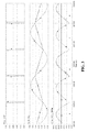
- the distinct phase circuits are driven at the same frequency and the driving signals of the power switches are mutually outphased by 120°, making the currents of the output diodes superpose with continuity. This functioning condition is illustrated in the time graphs of FIG. 5 .
- the functioning of a single LLC resonant phase is quantitatively described by means of characteristic curves as the ones depicted in FIG. 6 .
- the abscissa is the operating frequency x, normalized to the series resonance frequency associated to the elements Cr and Ls of the resonant circuit of FIG. 2
- the ordinate is the ratio M between the voltage on the nodes of the secondary winding, equal to the sum of the output voltage and of the voltage drop on the secondary rectifiers translated to the primary circuit, and the input voltage.
- Each characteristic curve is associated to the quality factor Q of the resonant circuit, that is inversely proportional to the output resistance R OUT .
- Q is substantially proportional to the output current I OUT and each curve is substantially associated to a value of the load current.
- the three phase circuits are powered with the same input voltage, they "see” the same output voltage and work at the same frequency. If the three phase circuits are exactly identical among them, they will work with the same current amplitude, as shown in FIG. 5 .
- the three phase circuits may have different values of the ratio M , because of the effect of different voltage drops on the respective secondary rectifiers and of different values of x and/or of the proportionality constant between Q and I OUT because of differences among the values of Ls, Cr and Lp of the three resonant circuits.
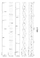
- the currents in the various phase circuits will differ among them, and one of them may even provide the whole power required by the load and the other phases be inactive.
- the average output current of phase circuit 1 is reduced by 97.4%, that of phase circuit 2 is increased by 297%, that of phase circuit 3 is zero; the peak-to-peak amplitude of the ripple of the output current, divided by its mean value, has changed from 17.8% to 165%.
- the rms value of the output current divided by the mean value is 114%, the rms value of the AC component is 55% of the mean value. As could have been expected, these values resemble those of a single phase LLC resonant voltage converter.
- a novel architecture of multi-phase resonant converters has been found capable of maintaining a good balancing of the currents in each phase even in presence of relevant differences among the components of the respective power circuits.
- the primary windings of the converter are star connected and the real neutral point of the star is coupled to a node at a reference potential through a normally open auxiliary switch.
- This switch may be closed at low load currents for turning off all the phases of the converter except one.
- the converter has a control circuit capable of generating PWM driving signals mutually outphased in function of outphasing signals input to the control circuit.
- Current sensors of the current circulating in each of the primary or secondary windings are adapted to generate respective sensing signals and a circuit compares the sensing signals and generates outphasing signals that are input to the control circuit.
- a novel control method of the multi-phase resonant converters is also provided. It contemplates the steps of driving only the half-bridge of a phase, leaving on the low-side switch of the half-bridge of another phase, and turning off the other half-bridges of the resonant converter when the supplied current delivered by the converter becomes smaller than a pre-established minimum threshold.
- novel methods may be used with any configuration of the resonant circuit, for example LLC, LCC or other, independently from the number of phases of the converter, by connecting the power circuits in such a way as to leave floating the real or virtual neutral point of the primary or of the secondary.
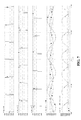
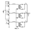
- FIG. 9 A three-phase LLC resonant DC-DC voltage converter capable of limiting unbalance among phase currents is depicted in FIG. 9 .
- the three LLC resonant circuits on the primary side are connected to a floating common node (real neutral point), differently from the prior art converter of FIG. 4 where the neutral point is grounded.
- the multi-phase resonant DC-DC voltage converter of this disclosure may be controlled using the same driving signals outphased by 120° of the half-bridges of the prior art converter of FIG. 4 .
- phase currents are far more uniform than in the known converter of FIG. 4 .
- the converter of FIG. 9 may be satisfactorily used though adjusting the mutual outphasing between driving signals of the half-bridges.
- Outphasing introduces a degree of freedom, that is a control variable for implementing a regulation loop aimed to nullify any residual unbalance among the phase currents.
- Control may be implemented by leaving fixed a phase circuit driving it with unmodified drive signals and modulating the driving signals of the other phase circuits, or by modulating all the driving signals of the phase circuits, etc.. The skilled designer will choose the most appropriate control technique in consideration of design specifications, characteristics, performances of the converter and cost restraints.
- the novel multi-phase resonant converter may be controlled also by driving only two phase circuits and leaving isolated the other phase circuit(s) eventually present, as illustrated in the time diagram of FIG. 13 , such to improve the conversion efficiency. As it may be noticed, even in this functioning condition the two active phases are perfectly balanced.
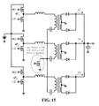
- FIG. 15 depicts another embodiment of the multiphase converter, having a normally off auxiliary switch for grounding the real neutral point of the primary circuit. If the converter has to deliver a relatively low output current, only a half-bridge is driven and the other half-bridges are kept off and the auxiliary switch is closed. An exemplary time diagram obtained in this functioning condition is depicted in FIG. 16 .
- phase regulation loop when only two phase circuits are active, it appears convenient to drive the two half-bridges in phase opposition: when the third phase circuit is switched off, the phase regulation loop, if present, is disabled and the outphasing varies from 120° (or a value not much different from this value, in case the phase regulation loop is present) to 180°. In this case the converter is driven in full-bridge mode.
- both the inductances as well as the resonant capacitances are composed in series. If the two resonant circuits were identical, the resonance frequency would not change; the characteristic impedance doubles but, since the two secondary circuits are electrically in parallel, the quality factor Q remains unchanged. As a matter of fact, small differences are present because the two resonant circuits do not match exactly and thus the regulation loop of the output voltage of the converter should act in a limited manner for correcting the working frequency.
- One or more low-side MOSFETs of the inactive half-bridges may be kept on for allowing current circulate through a single phase circuit.
- the resonant circuit switching from two active phase circuits to one active phase circuit, is not (nominally) altered; nevertheless, the functioning conditions switch abruptly from a full-bridge to a half-bridge mode, consequently halving the gain.
- This calls the regulation loop of the output voltage of the converter to a heavy intervention for compensating the abrupt gain variation with an appropriate reduction of the working frequency.
- FIGs. 17a-17c Other exemplary architectures of multiphase resonant converters are depicted in FIGs. 17a-17c .
- These converters have sensors of the current circulating in the primary or secondary windings, adapted to generate respective sensing signals, and a comparison circuit that generates outphasing signals by comparing the sensing signals among each other. These outphasing signals are used for adjusting mutual outphasing among the driving signals of the half-bridges, such to further balance the functioning conditions of the distinct phase circuits of the converter.
- the comparison circuit senses the difference between the currents of the phase circuit 1 ( ⁇ 1) and of the phase circuit 2 ( ⁇ 2) and between the currents of the phase circuit 2 ( ⁇ 2) and of the phase circuit 3 ( ⁇ 3), generating outphasing signals ( ⁇ 1-2 , ⁇ 2-3 ). Using these outphasing signals, mutual outphasing between the driving signal of MOSFETs of phase circuit 2 in respect to that of phase circuit 1 (that, for example, may be considered as a reference) and the outphasing between the driving signals of the MOSFETs of phase circuit 3 in respect to that of phase circuit 2 is adjusted.
- Table 2 shows exemplary comparison data for evaluating the effect of correction carried out by the outphasing regulation loop and the consequent reduction of unbalance among the output currents of the distinct phase circuit.
- Table 2 Load current No outphasing control With outphasing control 5 A DC output current of phase circuit 1 1,64 A (-1.2%) 1.64 A (-2.6%) DC output current of phase circuit 2 1.60 A (-10.2%) 1.73 A (+2.6%) DC output current of phase circuit 3 1.85 A (+11.2%) 1.67 A (0%) 6 A DC output current of phase circuit 1 1,98 A (-1.65%) 1.94 A (-3.6%) DC output current of phase circuit 2 1.84 A (-8.6%) 2.08 A (3.1 %) DC output current of phase circuit 3 2.23 A (10.4%) 2.02 A (0.33%)
- the values of parameters of the outphasing regulation loop for correcting the residual unbalance among the phase currents may be even different from the above indicated values, being designed according to the characteristics of the application in which the converter is to be used.
- the converter may work with only two active phase circuits for loads smaller than 15% of the maximum load and with a single active phase circuit for loads smaller than 10% of the maximum load.
- the optimal compromise between the two requirements will be determined by design considering specifications, characteristics, performances of the converter and cost restraints.
- FIG. 20 Another example of a three-phase LLC resonant voltage converter having an intrinsic ability of limiting unbalance among phase currents is depicted in FIG. 20 .
- the three LLC resonant circuits at the primary are connected to the isolated real neutral point; the transformers have a single secondary (having half the number of turns of the secondary windings of the transformers used in the architecture of FIG. 9 ) and the three circuits are connected to a floating neutral-point of the secondary circuit, the rectifiers forming a three-phase bridge.
- FIG. 21 shows the waveforms of the driving signals of the half-bridges (also in this case outphased by 120°) and the waveforms of the primary and secondary currents of the converter of FIG. 20 in case the reference capacitors Cr are not identical for all the phase circuits, but the capacitor of the phase circuit 2 is reduced by 10% and the capacitor of the phase circuit 3 is increased by 10%.
- the residual unbalance and the peak-to-peak ripple are slightly smaller.
- the architecture of the converter of this disclosure simplifies the realization of the transformer: it is not necessary to realize two accurately symmetrical secondary windings as in known converters with split (center-tap) secondary winding.
- the number of turns is halved, but the rms current that flows therethrough is doubled thus, neglecting high frequency effects, with the same amount of copper used for the windings, conduction losses remain the same; however, because of the reduced number of turns, the magnitude of high frequency effects is reduced.
- the neutral point of the secondary circuit is floating, it is no longer necessary to leave floating also the neutral point of the primary circuit (grounding it as shown in FIG. 20 ), however the converter architecture remains effective in reducing unbalance among the phase currents.
- FIG. 23 illustrates a further embodiment of a three-phase LLC resonant circuit intrinsically capable of limiting the unbalance among the phase currents.
- the connections of the secondary circuits are the same and the primary circuits are triangle connected. Even in this case, the neutral point (that in this configuration is virtual and not real) is floating. Given that the primary voltage is larger, the number of turns of the secondary windings is smaller than that of the architecture of FIG. 20 .
- FIG. 24 shows the waveforms of the driving signals of the half-bridges (also in this case outphased by 120°) and the waveforms of the primary and secondary currents when the capacitance of the phase circuit 2 is reduced by 10% and the capacitance of the phase circuit 3 is increased by 10%.
- the conditions used for testing the previous architectures are slightly smaller than the other architectures the residual unbalance and the increase of the output current ripple.
- this architecture it is possible to further reduce the unbalance among the phase currents by employing an outphasing control loop, as for the other two previously described architectures.
Abstract
Description
- This invention relates to voltage converters and more particularly to switching resonant voltage converters.
-
FIG. 1 is a high level block diagram of a switching resonant voltage converter. - Among resonant voltage converters having the basic architecture of
FIG. 1 and that are classified depending upon the configuration of the resonant circuit that is used, there is the so-called LLC resonant voltage converter. A half-bridge driven architecture of such a converter is depicted inFIG. 2 . - For simplicity sake, reference will be made to half-bridge driven voltage converters, though the addressed technical problems affect also full-bridge driven voltage converters.
- One of the weak points of this architecture, especially when functioning at high power levels (> 1 kW), is tied to the AC current that flows through the output capacitor COUT. This AC current has large peak and rms values that require the use of a larger and thus more encumbering bank of capacitors for realizing the capacitance COUT than for a forward voltage converter of the same output voltage and power. This considerably burdens the LLC resonant converter, especially in power applications of relatively large power density such as, for example, power supply systems for servers or for telecommunication systems in which its high efficiency characteristic is particularly advantageous.
- The so-called multi-phase or "interleaving" techniques allow to obviate to this drawback. A multi-phase voltage converter is obtained by connecting in parallel two or more switching converters of same architecture, such to make them share the same input voltage generator and supply the same output load. Moreover, with an appropriate phase control of the driving signals of the power switches, it is possible to minimize or, in certain cases, even to practically nullify the ripple on the output current (sometimes even on the input current) of the converters.
- Other advantages of the multi-phase approach are the possibility of subdividing the overall power requirement among a number of smaller converters making thus possible a larger power density and optimizing efficiency over a larger interval of load currents using the so-called "phase shedding" technique, that is turning off one or more phases when load decreases managing the reduced requirement with a reduced number of converters, thus reducing losses due to parasitic components of the power circuits, that may become dominant with low power conditions.
- The interleaving technique achieves:
- 1) reduction of the ripple of the output and of the input currents of the converter;
- 2) reduction of the power managed by each converter with a consequent optimization of their dimensioning;
- 3) optimization of the efficiency over a wide range of output load because of the possibility of turning off one or more phase circuits when functioning at low power and reduction of losses due to parasitic components;
- 4) greater power density and smaller form factor.
- In order to achieve the above beneficial effects, it is essential to ensure that the load of the converter be subdivided as equally as possible among the phase circuits. This is a serious obstacle to implementation of "interleaving" techniques in multi-phase resonant voltage converters.
- In order to better illustrate the problem, reference is made to the three-phase LLC resonant voltage converter of
FIG. 4 , though the same considerations hold mutatis mutandis also for resonant converters of different type and with any number of phases. - The distinct phase circuits are driven at the same frequency and the driving signals of the power switches are mutually outphased by 120°, making the currents of the output diodes superpose with continuity. This functioning condition is illustrated in the time graphs of
FIG. 5 . - In a first harmonic approximation, the functioning of a single LLC resonant phase is quantitatively described by means of characteristic curves as the ones depicted in
FIG. 6 . In these figures the abscissa is the operating frequency x, normalized to the series resonance frequency associated to the elements Cr and Ls of the resonant circuit ofFIG. 2 , and the ordinate is the ratio M between the voltage on the nodes of the secondary winding, equal to the sum of the output voltage and of the voltage drop on the secondary rectifiers translated to the primary circuit, and the input voltage. Each characteristic curve is associated to the quality factor Q of the resonant circuit, that is inversely proportional to the output resistance ROUT. As a consequence, Q is substantially proportional to the output current IOUT and each curve is substantially associated to a value of the load current. - The three phase circuits are powered with the same input voltage, they "see" the same output voltage and work at the same frequency. If the three phase circuits are exactly identical among them, they will work with the same current amplitude, as shown in
FIG. 5 . - Nevertheless, in a real case world implementation the inevitable tolerances of the components must be taken into consideration. Thus the three phase circuits may have different values of the ratio M, because of the effect of different voltage drops on the respective secondary rectifiers and of different values of x and/or of the proportionality constant between Q and IOUT because of differences among the values of Ls, Cr and Lp of the three resonant circuits. As a consequence, the currents in the various phase circuits will differ among them, and one of them may even provide the whole power required by the load and the other phases be inactive.
- These theoretical predictions are confirmed by simulation. In the diagrams of
FIG. 7 the same signals ofFIG. 5 relating to the converter ofFIG. 4 are shown, but the value of the capacitor Cr of thephase circuit 2 is reduced by 10% and that ofphase circuit 3 is increased by 10%. The currents through thephase circuits phase circuit 2 is almost equal to the output current. As a matter of fact, thesole phase circuit 2 is effectively working and there is no interleaving among the phase circuits. More precisely, compared with the ideal case ofFIG. 5 , the average output current ofphase circuit 1 is reduced by 97.4%, that ofphase circuit 2 is increased by 297%, that ofphase circuit 3 is zero; the peak-to-peak amplitude of the ripple of the output current, divided by its mean value, has changed from 17.8% to 165%. The rms value of the output current divided by the mean value is 114%, the rms value of the AC component is 55% of the mean value. As could have been expected, these values resemble those of a single phase LLC resonant voltage converter. - This situation, verified in an exemplary test case, is unacceptable because it would force to size each phase converter for delivering the whole output power, without any reduction of the ripple of the output current.
- In the published
US patent application No. 2008/0298093 Al "Multi-phase resonant converters for DC-DC application", a three-phase LLC resonant voltage converter composed of three half-bridges connected to the same input bus is disclosed (re: the architecture ofFIG. 4 , in which a further phase circuit in parallel to the two depicted phase circuits has been added), sustaining that it is naturally capable of balancing the phase currents. As a matter of fact, only the ideal case of exactly identical converters is considered, neglecting spreads among the components. - In the patent
US 6,970,366 , "Phase-shifted resonant converter having reduced output ripple", a system of two LLC resonant converters, synchronized and mutually outphased by 90° to minimize the overall ripple is disclosed. The document is silent about the problem of balancing the two phases. - In the article by H. Figge et al. "Paralleling of LLC resonant converter using frequency controlled current balancing", IEEE PESC 2008, June 2008, pp. 1080-1085, a system is proposed in which a DC-DC buck conversion stage is installed upstream of a two-phases LLC resonant converter. The regulation loop of the output voltage modulates the voltage generated by the buck (and, thus, the input voltage of the two half-bridges), a regulation loop of the balancing of the currents through the two phases determines the switching frequency of the half-bridges, that are outphased by 90°. This architecture solves the problem of balancing the currents at the cost of employing an additional conversion stage that, obviously, reduces overall efficiency and increases the overall complexity of the converter circuit.
- The degree of freedom necessary to balance the currents could be provided by duty-cycle adjustment: in this way, the mean value of the voltage applied to each phase would be adjustable. Nevertheless, as shown in the simulations of
FIG. 8 , this approach may be followed only if small adjustments are sufficient for obtaining a satisfactory balancing. Indeed, a duty-cycle significantly different from 50% would generate strongly asymmetrical currents in the secondary windings of the transformer and in the output diodes, thus the balancing problem would be merely shifted elsewhere. For implementing this method, the reactive components of the resonating circuits would have to be selected accurately, which is costly. - The recognized problems of known interleaved resonant architectures could be resumed as their marked sensitivity to differences among the power circuits and difficulty of finding a control variable that would be conveniently used for compensating the consequent unbalancing of the currents among the single phase circuits, which is an indispensable condition for reducing the ripple of the output current, which is the main reason for implementing the interleaving.
- A novel architecture of multi-phase resonant converters has been found capable of maintaining a good balancing of the currents in each phase even in presence of relevant differences among the components of the respective power circuits.
- This is achieved by connecting the primary windings and/or the secondary windings of the multi-phase converter such to leave floating the respective real or virtual neutral point.
- According to an embodiment, the primary windings of the converter are star connected and the real neutral point of the star is coupled to a node at a reference potential through a normally open auxiliary switch. This switch may be closed at low load currents for turning off all the phases of the converter except one.
- According to another embodiment, the converter has a control circuit capable of generating PWM driving signals mutually outphased in function of outphasing signals input to the control circuit. Current sensors of the current circulating in each of the primary or secondary windings are adapted to generate respective sensing signals and a circuit compares the sensing signals and generates outphasing signals that are input to the control circuit. With this architecture a novel control method is implemented according to which the PWM driving signals are mutually outphased for compensating eventual residual current unbalances.
- A novel control method of the multi-phase resonant converters is also provided. It contemplates the steps of driving only the half-bridge of a phase, leaving on the low-side switch of the half-bridge of another phase, and turning off the other half-bridges of the resonant converter when the supplied current delivered by the converter becomes smaller than a pre-established minimum threshold.
- The novel methods may be used with any configuration of the resonant circuit, for example LLC, LCC or other, independently from the number of phases of the converter, by connecting the power circuits in such a way as to leave floating the real or virtual neutral point of the primary or of the secondary.
-
-
FIG. 1 is a high level block diagram of a typical resonant DC-DC converter. -
FIG. 2 depicts a LLC resonant half-bridge with split (center-tap) secondary windings and full wave rectification through diodes. -
FIG. 3 are typical waveforms of the converter ofFIG. 2 when operating near the resonance frequency associated to components Ls and Cr. -
FIG. 4 shows an exemplary known three-phase LLC resonant converter wherein the interleaving is obtained by outphasing by 120° the driving signals of the three half-bridges. -
FIG. 5 are driving signals and currents through each phase of the converter of -
FIG. 4 with hypothetically identical phases. -
FIG. 6 illustrates the transfer characteristic of a half-bridge driven LLC resonant converter. -
FIG. 7 are waveforms similar to those ofFIG. 5 , in case the capacitance of thephase circuit 2 is reduced by 10% and the capacitance of thephase circuit 3 is increased by 10%. -
FIG.s 8a to 8c illustrate the effects of a duty-cycle unbalance in a phase circuit. -
FIG. 9 shows an embodiment of a novel three-phase LLC resonant converter with isolated neutral point on the primary side. -
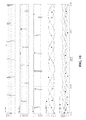
FIG. 10 are time diagrams of driving signals and of the currents of the phase circuits for the converter ofFIG. 9 , under the same conditions of unbalance ofFIG. 7 . -
FIG.s 11a to 11d show the primary currents and the results of the measurements of the DC output currents of the phases for the converter ofFIG. 9 for the values specified in Table 1. -
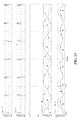
FIG.s 12a to 12d show the primary currents and the results of measurements of the DC output currents of the phase circuits for the converter ofFIG. 9 with the values specified in Table 1 with a further capacitor of 2.7nF in parallel to the resonant capacitor ofphase circuit 3. -
FIG. 13 are waveforms of the main signals of the converter ofFIG. 9 when the phase circuits ϕ1 and ϕ2 are active. -
FIG. 14 are waveforms of the main signals of the converter ofFIG. 9 when the sole phase circuit ϕ1 is active. -
FIG. 15 are an alternative embodiment of the converter ofFIG. 9 with normally open auxiliary switch, that may be eventually closed for grounding the primary real neutral point when only one phase circuit is active. -
FIG. 16 are waveforms of the main signals of the converter ofFIG. 15 when the sole phase circuit ϕ1 is active and the auxiliary switch is closed. -
FIG.s 17a to 17c are non-limiting examples of regulation loops of the mutual outphasing of the single phase circuits for nullifying the residual unbalancing of the output currents of each phase circuit. -
FIG. 18 is an exemplary diagram of the conversion efficiency of the converter with the parameters defined in Table 1, in function of the number of active phase circuits. -
FIG. 19 is a diagram of the results of simulations of the amplitude of the peak-to-peak ripple of the output current of the converter with the parameters defined in Table 1 in function of the number of active phase circuits. -
FIG. 20 shows a second embodiment of a three-phase LLC resonant converter capable of self-balancing the phase currents. -
FIG. 21 are time diagrams of the driving signals and of the phase currents for the converter ofFIG. 20 , with isolated neutral point at the primary, under the same conditions of unbalance of the waveforms ofFIG. 7 . -
FIG. 22 are time diagrams of the driving signal and of the phase currents for the converter ofFIG. 20 with grounded neutral point at the primary, under the same conditions of unbalance ofFIG. 7 . -
FIG. 23 shows a third embodiment of a three-phase LLC resonant converter capable of self-balancing the phase currents. -
FIG. 24 are time diagrams of driving signals and of the phase currents of the converter ofFIG. 23 , in the same conditions of unbalance ofFIG. 7 . - Several exemplary embodiments of this invention will be described making reference to a three-phase LLC resonant voltage converter, but the same considerations hold mutatis mutandis also for multi-phase resonant voltage converters of different type and/or with any other number of phases.
- A three-phase LLC resonant DC-DC voltage converter capable of limiting unbalance among phase currents is depicted in
FIG. 9 . The three LLC resonant circuits on the primary side are connected to a floating common node (real neutral point), differently from the prior art converter ofFIG. 4 where the neutral point is grounded. The multi-phase resonant DC-DC voltage converter of this disclosure may be controlled using the same driving signals outphased by 120° of the half-bridges of the prior art converter ofFIG. 4 . - The fact that the potential of the neutral-point is not grounded, introduces a "negative feedback" that tends to equilibrate the working points of the single phase circuits, thus preventing that a single phase circuit deliver the whole current required by the load whilst the other phase circuits are practically inactive. This is evident in the graphs of
FIG. 10 that depict waveforms obtained using the same driving signals used for obtaining the diagrams ofFIG. 7 relative to the prior art converter ofFIG. 5 under the same unbalance conditions. - In the multi-phase resonant voltage converter of this disclosure, the phase currents are far more uniform than in the known converter of
FIG. 4 . - By comparing the time diagrams of
FIG. 10 with those ofFIG. 7 , it may be recognized inferred that in the former case all three phases are working, with a maximum unbalance that is 14 times smaller than that ofFIG. 7 ; the peak-to-peak amplitude of the output current waveform is reduced by a factor larger than 3 and the rms value of the AC current by a factor of about 4. - These outstanding results are substantially confirmed also by measurements shown in the diagrams of
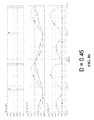
FIG.s 11 and12 , carried out on a prototype realized according to the scheme ofFIG. 9 , with the design parameters shown in Table 1:Table 1 Minimum DC input voltage Vin_min 320 V Nominal DC input voltage Vin 390 V Maximum DC input voltage Vin_max 420 V Regulated output voltage Vout 24 V Maximum output current lout 8 A Nominal resonant capacitor Cr 22 nF Leakage inductance Lr 110 µH Magnetization inductance Lm 585 µH Nominal resonant frequency Fr 100 kHz Output capacitor Cout 100 µF - In many applications, the performances of the converter of
FIG. 9 , in terms of phase current balance, would be quite acceptable and not requiring any specific further action for improving it. - In applications where an enhanced balance of the phase currents is required, the converter of
FIG. 9 may be satisfactorily used though adjusting the mutual outphasing between driving signals of the half-bridges. Outphasing introduces a degree of freedom, that is a control variable for implementing a regulation loop aimed to nullify any residual unbalance among the phase currents. - Well known techniques for carrying out such a feedback control may be easily implemented by any skilled person. For example, it is possible to sense the secondary currents or the resonant primary currents; the sensing may be performed through current transformer or through sensing resistors; the error signals may be generated and processed through mutual comparisons and/or with reference values, or by the use of error amplifiers with frequency compensations, or even through analog or digital processing. Control may be implemented by leaving fixed a phase circuit driving it with unmodified drive signals and modulating the driving signals of the other phase circuits, or by modulating all the driving signals of the phase circuits, etc.. The skilled designer will choose the most appropriate control technique in consideration of design specifications, characteristics, performances of the converter and cost restraints.
- When the output load is relatively low, the novel multi-phase resonant converter may be controlled also by driving only two phase circuits and leaving isolated the other phase circuit(s) eventually present, as illustrated in the time diagram of
FIG. 13 , such to improve the conversion efficiency. As it may be noticed, even in this functioning condition the two active phases are perfectly balanced. - It is possible also to drive a single half-bridge of the novel multi-phase resonant converter when the converter should deliver relatively low currents, by keeping on only one or more low-side switches of another half-bridge in order to close the circuit. Exemplary time diagrams obtained by driving the converter of
FIG. 9 in such a functioning condition are shown inFIG. 14 . -
FIG. 15 depicts another embodiment of the multiphase converter, having a normally off auxiliary switch for grounding the real neutral point of the primary circuit. If the converter has to deliver a relatively low output current, only a half-bridge is driven and the other half-bridges are kept off and the auxiliary switch is closed. An exemplary time diagram obtained in this functioning condition is depicted inFIG. 16 . - Experimental results, illustrated in the diagram of
FIG. 18 , show that the efficiency improvesat medium-low load conditions. Therefore, it is advisable to turn off a phase circuit when the load decreases below 55% of the maximum rated load and operating with a single phase circuit when the load becomes smaller than 30% of the maximum load. - When only two phase circuits are active, it appears convenient to drive the two half-bridges in phase opposition: when the third phase circuit is switched off, the phase regulation loop, if present, is disabled and the outphasing varies from 120° (or a value not much different from this value, in case the phase regulation loop is present) to 180°. In this case the converter is driven in full-bridge mode.
- The characteristics of the resonant circuit are only slightly modified: both the inductances as well as the resonant capacitances are composed in series. If the two resonant circuits were identical, the resonance frequency would not change; the characteristic impedance doubles but, since the two secondary circuits are electrically in parallel, the quality factor Q remains unchanged. As a matter of fact, small differences are present because the two resonant circuits do not match exactly and thus the regulation loop of the output voltage of the converter should act in a limited manner for correcting the working frequency.
- One or more low-side MOSFETs of the inactive half-bridges may be kept on for allowing current circulate through a single phase circuit. In the first case the resonant circuit, switching from two active phase circuits to one active phase circuit, is not (nominally) altered; nevertheless, the functioning conditions switch abruptly from a full-bridge to a half-bridge mode, consequently halving the gain. This calls the regulation loop of the output voltage of the converter to a heavy intervention for compensating the abrupt gain variation with an appropriate reduction of the working frequency. In the latter case, all phase circuits participate to the delivery of energy (even if in an unbalanced manner) but with a great variation of the characteristics of the resonant circuit, thus also in this case the regulation loop of the output voltage must be able to reduce the working frequency.
- Other exemplary architectures of multiphase resonant converters are depicted in
FIGs. 17a-17c . These converters have sensors of the current circulating in the primary or secondary windings, adapted to generate respective sensing signals, and a comparison circuit that generates outphasing signals by comparing the sensing signals among each other. These outphasing signals are used for adjusting mutual outphasing among the driving signals of the half-bridges, such to further balance the functioning conditions of the distinct phase circuits of the converter. - According to an embodiment, the comparison circuit senses the difference between the currents of the phase circuit 1 (ϕ1) and of the phase circuit 2 (ϕ2) and between the currents of the phase circuit 2 (ϕ2) and of the phase circuit 3 (ϕ3), generating outphasing signals (Δϕ1-2, Δϕ2-3). Using these outphasing signals, mutual outphasing between the driving signal of MOSFETs of
phase circuit 2 in respect to that of phase circuit 1 (that, for example, may be considered as a reference) and the outphasing between the driving signals of the MOSFETs ofphase circuit 3 in respect to that ofphase circuit 2 is adjusted. Table 2 shows exemplary comparison data for evaluating the effect of correction carried out by the outphasing regulation loop and the consequent reduction of unbalance among the output currents of the distinct phase circuit.Table 2 Load
currentNo outphasing
controlWith outphasing
control5 A DC output current of phase circuit 11,64 A (-1.2%) 1.64 A (-2.6%) DC output current of phase circuit 21.60 A (-10.2%) 1.73 A (+2.6%) DC output current of phase circuit 31.85 A (+11.2%) 1.67 A (0%) 6 A DC output current of phase circuit 11,98 A (-1.65%) 1.94 A (-3.6%) DC output current of phase circuit 21.84 A (-8.6%) 2.08 A (3.1 %) DC output current of phase circuit 32.23 A (10.4%) 2.02 A (0.33%) - The values of parameters of the outphasing regulation loop for correcting the residual unbalance among the phase currents may be even different from the above indicated values, being designed according to the characteristics of the application in which the converter is to be used.
- The results of a simulation carried out on one of the converters of
FIG. 17 with the parameters indicated in Table 1 are shown inFIG. 19 . To make the output current ripple not exceed the value attained at maximum load when all the three phase circuits are active, the converter may work with only two active phase circuits for loads smaller than 15% of the maximum load and with a single active phase circuit for loads smaller than 10% of the maximum load. The optimal compromise between the two requirements will be determined by design considering specifications, characteristics, performances of the converter and cost restraints. - Another example of a three-phase LLC resonant voltage converter having an intrinsic ability of limiting unbalance among phase currents is depicted in
FIG. 20 . Even in this case the three LLC resonant circuits at the primary are connected to the isolated real neutral point; the transformers have a single secondary (having half the number of turns of the secondary windings of the transformers used in the architecture ofFIG. 9 ) and the three circuits are connected to a floating neutral-point of the secondary circuit, the rectifiers forming a three-phase bridge. -
FIG. 21 shows the waveforms of the driving signals of the half-bridges (also in this case outphased by 120°) and the waveforms of the primary and secondary currents of the converter ofFIG. 20 in case the reference capacitors Cr are not identical for all the phase circuits, but the capacitor of thephase circuit 2 is reduced by 10% and the capacitor of thephase circuit 3 is increased by 10%. In these conditions similar to those used for treating the architecture of the preceding embodiment, the residual unbalance and the peak-to-peak ripple are slightly smaller. - The architecture of the converter of this disclosure simplifies the realization of the transformer: it is not necessary to realize two accurately symmetrical secondary windings as in known converters with split (center-tap) secondary winding. The number of turns is halved, but the rms current that flows therethrough is doubled thus, neglecting high frequency effects, with the same amount of copper used for the windings, conduction losses remain the same; however, because of the reduced number of turns, the magnitude of high frequency effects is reduced.
- Because the neutral point of the secondary circuit is floating, it is no longer necessary to leave floating also the neutral point of the primary circuit (grounding it as shown in
FIG. 20 ), however the converter architecture remains effective in reducing unbalance among the phase currents. - The results of simulations of
FIG. 22 show only marginal differences in respect to those ofFIG. 21 , with only a slight deformation of primary currents, whilst the secondary currents remain substantially unchanged and performance is substantially the same. With this architecture, whether the primary neutral point is floating or not, it is possible to further reduce the unbalance among the phase currents through an outphasing control loop. This outphasing control may be employed also for the topology ofFIG. 9 . -
FIG. 23 illustrates a further embodiment of a three-phase LLC resonant circuit intrinsically capable of limiting the unbalance among the phase currents. Compared to the architecture ofFIG. 20 , the connections of the secondary circuits are the same and the primary circuits are triangle connected. Even in this case, the neutral point (that in this configuration is virtual and not real) is floating. Given that the primary voltage is larger, the number of turns of the secondary windings is smaller than that of the architecture ofFIG. 20 . -
FIG. 24 shows the waveforms of the driving signals of the half-bridges (also in this case outphased by 120°) and the waveforms of the primary and secondary currents when the capacitance of thephase circuit 2 is reduced by 10% and the capacitance of thephase circuit 3 is increased by 10%. Compared to the conditions used for testing the previous architectures, are slightly smaller than the other architectures the residual unbalance and the increase of the output current ripple. Also for this architecture it is possible to further reduce the unbalance among the phase currents by employing an outphasing control loop, as for the other two previously described architectures. - The claims as filed are integral part of the description and are herein incorporated by reference.
Claims (12)
- A switching multi-phase resonant voltage converter, comprising a plurality of primary windings powered through respective half-bridges, as many secondary windings connected to an output terminal of the converter and magnetically coupled to the respective primary windings, a plurality of LLC resonant circuit each coupled to a respective one of said plurality of primary windings, characterized in that said primary or secondary windings are connected such that a real or virtual neutral point is floating.
- The multi-phase resonant voltage converter of claim 1, wherein said primary windings are either star-connected or polygon-connected.
- The multi-phase resonant voltage converter of claim 1, wherein said secondary windings are star connected, said converter comprising a multi-phase rectifying bridge connecting the other terminal not in common of the secondary windings to the output terminal of the converter.
- The multi-phase resonant voltage converter according to any of the previous claims, wherein said phase circuits are three.
- The multi-phase resonant voltage converter according to one of the previous claims, further comprising a control circuit adapted to generate PWM driving signals of said half-bridges mutually outphased in function of outphasing signals provided in input to the control circuit.
- The multi-phase resonant voltage converter of claim 5, further comprising:sensors of the current flowing through each of said primary windings, adapted to generate respective sensing signals;a circuit for comparing said sensing signals among each other, adapted to generate said outphasing signals.
- The multi-phase resonant voltage converter of claim 5, further comprising:sensors of the current flowing through each of said secondary windings, adapted to generate respective sensing signals;a circuit for comparing said sensing signals among each other, adapted to generate said outphasing signals.
- The multi-phase resonant voltage converter of claim 6, wherein said sensors of the current flowing through each of said primary windings sense the current during off phases (OFF).
- The resonant voltage converter of claim 1, wherein said primary windings are star-connected, further comprising a normally off switch adapted to ground said real neutral point when the load decreases below a minimum threshold.
- A method of controlling in switched mode a multi-phase resonant voltage converter, comprising a plurality of primary windings powered through respective half-bridges, as many secondary winding connected to an output terminal of the converter and magnetically coupled to the respective primary windings, a plurality of LLC resonant circuit each coupled to a respective one of said plurality of primary windings, said primary or secondary windings being connected such to keep floating a real or virtual neutral point, a control circuit adapted to generate PWM driving signals of said half-bridges, characterized in that the method comprises the step of adjusting mutual outphasing among the PWM driving signals of said half-bridges such to equilibrate the currents flowing through said windings.
- A method of controlling in switched mode a multi-phase resonant voltage converter, comprising a plurality of primary windings powered through respective half-bridges, as many secondary windings connected to an output terminal of the converter and magnetically coupled to the respective primary windings, a plurality of LLC resonant circuit each coupled to a respective one of said plurality of primary windings, said primary or secondary windings being star-connected, the real neutral point being floating, a control circuit adapted to generate PWM driving signals of said half-bridges, characterized in that the method comprises the step of driving only one of said half-bridges and leaving on a low-side switch of at least another of said half-bridges when the current delivered to the load by the converter is smaller than a minimum pre-established threshold.
- A method of controlling in switched mode a multi-phase resonant voltage converter, comprising a plurality of primary windings powered through respective half-bridges, as many secondary windings connected to an output terminal of the converter and magnetically coupled to respective primary windings, a plurality of LLC resonant circuit each coupled to a respective one of said plurality of primary windings, said primary or secondary windings being star connected, the real neutral point being coupled to a common ground node through a normally off switch, a control circuit adapted to generate PWM driving signals of said half-bridges, characterized in that the method comprises the step of driving only one of said half-bridges and switching on the auxiliary grounding switch of the real neutral point when the current delivered by the converter is smaller than a minimum pre-established threshold.
Applications Claiming Priority (1)
| Application Number | Priority Date | Filing Date | Title |
|---|---|---|---|
| ITVA20090038 | 2009-06-24 |
Publications (2)
| Publication Number | Publication Date |
|---|---|
| EP2299580A2 true EP2299580A2 (en) | 2011-03-23 |
| EP2299580A3 EP2299580A3 (en) | 2011-07-27 |
Family
ID=41611147
Family Applications (1)
| Application Number | Title | Priority Date | Filing Date |
|---|---|---|---|
| EP10166124A Withdrawn EP2299580A3 (en) | 2009-06-24 | 2010-06-16 | Multi-phase resonant converter and method of controlling it |
Country Status (3)
| Country | Link |
|---|---|
| US (4) | US9780678B2 (en) |
| EP (1) | EP2299580A3 (en) |
| CN (1) | CN101951152A (en) |
Cited By (11)
| Publication number | Priority date | Publication date | Assignee | Title |
|---|---|---|---|---|
| EP2514086A2 (en) * | 2009-12-17 | 2012-10-24 | Eltek AS | Resonant circuit and resonant dc/dc converter |
| WO2014040170A1 (en) * | 2012-09-14 | 2014-03-20 | Queen's University At Kingston | Interleaved resonant converter |
| WO2016001545A1 (en) | 2014-06-30 | 2016-01-07 | Valeo Systemes De Controle Moteur | Voltage converter comprising a resonance-based converter circuit |
| DE102014220434A1 (en) | 2014-10-09 | 2016-04-14 | Bayerische Motoren Werke Aktiengesellschaft | Efficient DC-DC converter with a wide working range |
| US9755522B2 (en) | 2013-04-23 | 2017-09-05 | Valeo Equipements Electriques Moteur | Method and device for controlling a multiphase resonant DC/DC converter, and corresponding multiphase converter |
| WO2018019100A1 (en) * | 2016-07-25 | 2018-02-01 | 中兴通讯股份有限公司 | Control method and device of three-phase half-bridge llc resonant converter |
| WO2020186978A1 (en) * | 2019-03-21 | 2020-09-24 | 湖南工程学院 | Method for realizing interphase current sharing of illc resonant converter and prolonging power-down hold-up time |
| EP3796528A1 (en) * | 2019-09-20 | 2021-03-24 | ABB Schweiz AG | Current balancing in power semiconductors of a dc/dc converter |
| EP3796529A1 (en) * | 2019-09-20 | 2021-03-24 | ABB Schweiz AG | Redundancy of a resonant converter stage by frequency adaptation |
| US11749433B2 (en) | 2019-03-05 | 2023-09-05 | Astec International Limited | Transformers having integrated magnetic structures for power converters |
| WO2023223998A1 (en) * | 2022-05-16 | 2023-11-23 | 株式会社Gsユアサ | Multiphase llc resonant converter circuit |
Families Citing this family (56)
| Publication number | Priority date | Publication date | Assignee | Title |
|---|---|---|---|---|
| EP2299580A3 (en) * | 2009-06-24 | 2011-07-27 | STMicroelectronics S.r.l. | Multi-phase resonant converter and method of controlling it |
| CN102403907B (en) * | 2009-07-07 | 2014-12-31 | 台达电子工业股份有限公司 | Multiphase switch power supply switching circuit |
| CN101944852B (en) * | 2009-07-07 | 2013-03-27 | 台达电子工业股份有限公司 | Multiphase switch power supply switching circuit |
| US8570913B2 (en) | 2009-12-11 | 2013-10-29 | Rf Micro Devices, Inc. | De-multiplexing a radio frequency input signal using output transformer circuitry |
| US8729963B2 (en) * | 2011-02-09 | 2014-05-20 | Rf Micro Devices, Inc. | Asymmetrical transformer output demultiplexing (atodem) circuit |
| US8923418B2 (en) | 2011-03-25 | 2014-12-30 | Rf Micro Devices, Inc. | Phase shifting stage for switchless de-multiplexing |
| CN102790533A (en) * | 2011-05-19 | 2012-11-21 | 中兴通讯股份有限公司 | Multi-phase alternating resonant converter |
| CN103828211B (en) | 2011-07-04 | 2017-07-14 | Abb 技术有限公司 | High pressure DC/DC converters |
| CN102545629A (en) * | 2011-12-26 | 2012-07-04 | 上海交通大学 | Power source for subway locomotive |
| US9072155B2 (en) * | 2012-06-22 | 2015-06-30 | Moxtek, Inc. | Transformer network |
| EP2683066B1 (en) | 2012-07-04 | 2017-05-03 | DET International Holding Limited | LLC balancing |
| CN102810992A (en) * | 2012-08-23 | 2012-12-05 | 襄阳九鼎昊天环保设备有限公司 | Three-phase L-C constant current source high-voltage power supply |
| US9083256B2 (en) * | 2012-12-21 | 2015-07-14 | Scandinova Systems Ab | Capacitor charger system, power modulator and resonant power converter |
| US9520790B2 (en) | 2013-03-15 | 2016-12-13 | General Electric Company | Interleaved LLC converters and current sharing method thereof |
| US9300214B2 (en) * | 2013-03-15 | 2016-03-29 | Power-One, Inc. | Multiphase converter with active and passive internal current sharing |
| CN104377961B (en) * | 2013-08-16 | 2017-09-15 | 台达电子企业管理(上海)有限公司 | The method of converter and reduction node voltage |
| US9337743B2 (en) | 2013-10-11 | 2016-05-10 | Futurewei Technologies, Inc. | Apparatus and method for multiple primary bridge resonant converters |
| CN104578791B (en) * | 2013-10-15 | 2018-01-23 | 南京博兰得电子科技有限公司 | Controlled resonant converter in parallel and its control method |
| JP2015139258A (en) | 2014-01-21 | 2015-07-30 | サンケン電気株式会社 | Switching power supply device |
| US9356521B2 (en) | 2014-01-30 | 2016-05-31 | Sanken Electric Co., Ltd. | Switching power-supply device having wide input voltage range |
| US9356519B2 (en) * | 2014-02-12 | 2016-05-31 | Sanken Electric Co., Ltd. | Current balance circuit of resonant type switching power-supply circuit |
| RU2563027C1 (en) * | 2014-05-07 | 2015-09-20 | Федеральное государственное бюджетное образовательное учреждение высшего профессионального образования "Южно-Уральский государственный университет" (национальный исследовательский университет) (ФГБОУ ВПО "ЮУрГУ" (НИУ)) | Method to control multi-phase rectifying unit |
| JP6295173B2 (en) * | 2014-05-19 | 2018-03-14 | ローム株式会社 | Power supply |
| TWI532305B (en) * | 2014-06-20 | 2016-05-01 | Asian Power Devices Inc | Parallel Resistive Resonant Converter Circuit with Current Sharing Function |
| US10110146B2 (en) | 2014-09-30 | 2018-10-23 | Lawrence Livermore National Security, Llc | Pulse-train drive system for electrostatic generators and motors |
| CN104578733A (en) * | 2015-02-04 | 2015-04-29 | 四川英杰电气股份有限公司 | Low ripple output method of tandem high-voltage DC power source |
| JP6580855B2 (en) * | 2015-04-03 | 2019-09-25 | トヨタ自動車株式会社 | Power receiving device and power transmitting device |
| CN108028606B (en) | 2015-09-18 | 2020-03-24 | 株式会社村田制作所 | Module parallel technology of resonant converter |
| WO2017049179A1 (en) | 2015-09-18 | 2017-03-23 | Murata Manufacturing Co., Ltd. | Converters with hold-up operation |
| CN106712517A (en) * | 2015-11-12 | 2017-05-24 | 华为技术有限公司 | Resonant bidirectional conversion circuit and converter |
| WO2017194164A1 (en) * | 2016-05-13 | 2017-11-16 | Huawei Technologies Co., Ltd. | Resonant dc-dc converter |
| KR101856008B1 (en) | 2016-06-30 | 2018-05-10 | 한국에너지기술연구원 | Interleaved llc resonant converter and control method thereof |
| US10395819B2 (en) * | 2016-08-30 | 2019-08-27 | Astec International Limited | Multiple phase power converters having integrated magnetic cores for transformer and inductor windings |
| US20180191168A1 (en) * | 2017-01-04 | 2018-07-05 | National Instruments Corporation | Parallel Interleaved Multiphase LLC Current Sharing Control |
| KR102105149B1 (en) * | 2017-05-26 | 2020-04-28 | 주식회사 솔루엠 | multi-level LLC resonant converter and electronic device |
| US20190181744A1 (en) * | 2017-12-11 | 2019-06-13 | Texas Instruments Incorporated | Bus converter current ripple reduction |
| US10205377B1 (en) * | 2018-04-09 | 2019-02-12 | Stmicroelectronics S.R.L. | Active clamp flyback converter control with reduced current |
| CN108429466B (en) * | 2018-04-12 | 2019-10-18 | 浙江大学 | A kind of three road output DC-DC converter of isolation hybrid modulation based on three-phase LLC resonance circuit and phase whole-bridging circuit |
| CN111361435B (en) * | 2018-12-25 | 2021-11-12 | 比亚迪股份有限公司 | Vehicle-mounted charger and control method and control device thereof |
| KR20210117319A (en) * | 2019-01-24 | 2021-09-28 | 마그나 인터내셔널 인코포레이티드 | Method and system for balancing a polyphase LLC power converter with switch controlled capacitors |
| US10658931B1 (en) | 2019-04-17 | 2020-05-19 | Apple Inc. | Digital current mode control for multi-phase voltage regulator circuits |
| IT201900006000A1 (en) | 2019-04-17 | 2020-10-17 | St Microelectronics Srl | A PROCEDURE FOR OPERATING A FLYBACK CONVERTER WITH AN ACTIVE CLAMP, CORRESPONDING CONTROL CIRCUIT AND FLYBACK CONVERTER |
| FR3101933B1 (en) * | 2019-10-15 | 2021-10-01 | Valeo Vision | LIGHTING SYSTEM INCLUDING A MULTI-PHASE INTERLACED POWER CONVERTER |
| US11283365B2 (en) | 2020-02-28 | 2022-03-22 | Astec International Limited | Switch-mode power supplies including three-level LLC circuits |
| JP2022015029A (en) * | 2020-07-08 | 2022-01-21 | オムロン株式会社 | Electric power conversion device and electric power system |
| CN111884515B (en) * | 2020-07-20 | 2021-07-27 | 华中科技大学 | Current detection method and device of LLC resonant converter |
| EP3965279A1 (en) * | 2020-09-04 | 2022-03-09 | Delta Electronics (Thailand) Public Co., Ltd. | Power balancing in interleaved llc converters via duty cycle variation |
| US11557976B2 (en) * | 2020-11-27 | 2023-01-17 | Astec International Limited | Three-phase LLC power supply circuit for high voltage bus input |
| JP2022101013A (en) * | 2020-12-24 | 2022-07-06 | オムロン株式会社 | Electric power conversion device and device and method for controlling electric power conversion device |
| US11742764B2 (en) * | 2021-02-04 | 2023-08-29 | Maxim Integrated Products, Inc. | Resonant power converters including coupled inductors |
| CN114928260A (en) * | 2021-02-10 | 2022-08-19 | 华为数字能源技术有限公司 | Control circuit for controlling converter, converter and power supply equipment |
| CN114337305A (en) * | 2021-12-31 | 2022-04-12 | 苏州汇川控制技术有限公司 | DC voltage conversion circuit and device |
| WO2023157916A1 (en) * | 2022-02-16 | 2023-08-24 | ニチコン株式会社 | Dc/dc converter |
| JP2023168843A (en) * | 2022-05-16 | 2023-11-29 | 株式会社Gsユアサ | Multi-phase llc resonant converter circuit |
| US11909324B2 (en) * | 2022-06-09 | 2024-02-20 | Dell Products L.P. | Trans-inductor voltage regulator using a nonlinear compensation inductor |
| CN116260344B (en) * | 2023-05-15 | 2024-03-08 | 西安图为电气技术有限公司 | Multiphase resonant circuit and power supply device |
Citations (2)
| Publication number | Priority date | Publication date | Assignee | Title |
|---|---|---|---|---|
| US6970366B2 (en) | 2003-04-03 | 2005-11-29 | Power-One As | Phase-shifted resonant converter having reduced output ripple |
| US20080298093A1 (en) | 2007-05-30 | 2008-12-04 | Taotao Jin | Multiphase resonant converter for dc-dc applications |
Family Cites Families (22)
| Publication number | Priority date | Publication date | Assignee | Title |
|---|---|---|---|---|
| US5737203A (en) * | 1994-10-03 | 1998-04-07 | Delco Electronics Corp. | Controlled-K resonating transformer |
| US5668707A (en) * | 1994-10-04 | 1997-09-16 | Delco Electronics Corp. | Multi-phase power converter with harmonic neutralization |
| US5535906A (en) * | 1995-01-30 | 1996-07-16 | Advanced Energy Industries, Inc. | Multi-phase DC plasma processing system |
| EA001816B1 (en) * | 1995-10-24 | 2001-08-27 | Аквагэс Нью Зиленд Лимитед | An ac-dc power supply |
| WO1997022173A1 (en) * | 1995-12-14 | 1997-06-19 | Philips Electronics N.V. | Power supply apparatus |
| DE19845903A1 (en) * | 1998-10-05 | 2000-04-06 | Aloys Wobben | Electrical power transmission system |
| JP2000324837A (en) * | 1999-04-23 | 2000-11-24 | Lg Electronics Inc | Dc power supply circuit |
| US6031747A (en) * | 1999-08-02 | 2000-02-29 | Lockheed Martin Missiles & Space Company | Interleaved synchronous flyback converter with high efficiency over a wide operating load range |
| US6246599B1 (en) * | 2000-08-25 | 2001-06-12 | Delta Electronics, Inc. | Constant frequency resonant inverters with a pair of resonant inductors |
| US7035125B2 (en) * | 2003-02-05 | 2006-04-25 | Matsushita Electric Industrial Co., Ltd. | Switching power supply and control method for the same |
| ITRE20040038A1 (en) * | 2004-04-22 | 2004-07-22 | Ask Ind Spa | THREE-PHASE DC / DC CONVERTER |
| JP3829142B2 (en) * | 2004-10-29 | 2006-10-04 | Tdk株式会社 | Discharge lamp driving device |
| US7414868B2 (en) * | 2005-06-20 | 2008-08-19 | Astec International Limited | Switched current power converter with partial converter decoupling for low load conditions |
| DE102005036806A1 (en) * | 2005-08-02 | 2007-02-08 | Lorch Schweißtechnik GmbH | Electric power source, in particular welding power source |
| US7307361B1 (en) * | 2006-11-13 | 2007-12-11 | Drs Power & Control Technologies, Inc. | Medium voltage power converter formed using low voltage drives |
| JP5104058B2 (en) * | 2007-06-21 | 2012-12-19 | サンケン電気株式会社 | Resonant switching power supply |
| ITVA20070065A1 (en) * | 2007-07-25 | 2009-01-26 | St Microelectronics Srl | METHOD AND PILOTING DEVICE FOR BRUSHLESS ENGINE WITH TENSIONING PROFILE PREPARED FOR PROGRESSIVE AND AUTOMATIC SWITCHING FROM A THREE-PHASE SINUSOIDAL TYPE PILOT TO A THREE-PHASE ON-SQUARE WAVE PLIOTURE |
| EP2263302B1 (en) * | 2008-03-06 | 2012-02-08 | Philips Intellectual Property & Standards GmbH | Dc/ac power inverter control unit of a resonant power converter circuit, in particular a dc/dc converter for use in a high-voltage generator circuitry of a modern computed tomography device or x-ray radiographic system |
| EP2299580A3 (en) * | 2009-06-24 | 2011-07-27 | STMicroelectronics S.r.l. | Multi-phase resonant converter and method of controlling it |
| CN101944852B (en) * | 2009-07-07 | 2013-03-27 | 台达电子工业股份有限公司 | Multiphase switch power supply switching circuit |
| FR3004870B1 (en) * | 2013-04-23 | 2015-05-22 | Valeo Equip Electr Moteur | METHOD AND DEVICE FOR CONTROLLING A RESONANCE CONTINUOUS CURRENT-CURRENT MULTI-PHASE CONVERTER, AND CORRESPONDING MULTIPHASE CONVERTER |
| JP6295173B2 (en) * | 2014-05-19 | 2018-03-14 | ローム株式会社 | Power supply |
-
2010
- 2010-06-16 EP EP10166124A patent/EP2299580A3/en not_active Withdrawn
- 2010-06-22 US US12/820,549 patent/US9780678B2/en active Active
- 2010-06-24 CN CN2010102613971A patent/CN101951152A/en active Pending
-
2017
- 2017-08-31 US US15/693,166 patent/US10193461B2/en active Active
-
2018
- 2018-12-06 US US16/211,619 patent/US10756637B2/en active Active
-
2020
- 2020-07-20 US US16/933,534 patent/US11329568B2/en active Active
Patent Citations (2)
| Publication number | Priority date | Publication date | Assignee | Title |
|---|---|---|---|---|
| US6970366B2 (en) | 2003-04-03 | 2005-11-29 | Power-One As | Phase-shifted resonant converter having reduced output ripple |
| US20080298093A1 (en) | 2007-05-30 | 2008-12-04 | Taotao Jin | Multiphase resonant converter for dc-dc applications |
Non-Patent Citations (1)
| Title |
|---|
| H. FIGGE ET AL.: "Paralleling of LLC resonant converter using frequency controlled current balancing", IEEE PESC, vol. 08, 20 June 2008 (2008-06-20), pages 1080 - 1085 |
Cited By (17)
| Publication number | Priority date | Publication date | Assignee | Title |
|---|---|---|---|---|
| EP2514086A2 (en) * | 2009-12-17 | 2012-10-24 | Eltek AS | Resonant circuit and resonant dc/dc converter |
| US9240723B2 (en) | 2009-12-17 | 2016-01-19 | Eltek As | Resonant circuit and resonant DC/DC converter |
| WO2014040170A1 (en) * | 2012-09-14 | 2014-03-20 | Queen's University At Kingston | Interleaved resonant converter |
| US9729070B2 (en) | 2012-09-14 | 2017-08-08 | Ganpower International Inc. | Interleaved resonant converter |
| US10476397B2 (en) | 2012-09-14 | 2019-11-12 | Ganpower International Inc. | Interleaved resonant converter |
| US9755522B2 (en) | 2013-04-23 | 2017-09-05 | Valeo Equipements Electriques Moteur | Method and device for controlling a multiphase resonant DC/DC converter, and corresponding multiphase converter |
| WO2016001545A1 (en) | 2014-06-30 | 2016-01-07 | Valeo Systemes De Controle Moteur | Voltage converter comprising a resonance-based converter circuit |
| DE102014220434A1 (en) | 2014-10-09 | 2016-04-14 | Bayerische Motoren Werke Aktiengesellschaft | Efficient DC-DC converter with a wide working range |
| CN107659161A (en) * | 2016-07-25 | 2018-02-02 | 中兴通讯股份有限公司 | A kind of control method and device of three-phase half-bridge LLC controlled resonant converters |
| WO2018019100A1 (en) * | 2016-07-25 | 2018-02-01 | 中兴通讯股份有限公司 | Control method and device of three-phase half-bridge llc resonant converter |
| US11749433B2 (en) | 2019-03-05 | 2023-09-05 | Astec International Limited | Transformers having integrated magnetic structures for power converters |
| WO2020186978A1 (en) * | 2019-03-21 | 2020-09-24 | 湖南工程学院 | Method for realizing interphase current sharing of illc resonant converter and prolonging power-down hold-up time |
| EP3796528A1 (en) * | 2019-09-20 | 2021-03-24 | ABB Schweiz AG | Current balancing in power semiconductors of a dc/dc converter |
| EP3796529A1 (en) * | 2019-09-20 | 2021-03-24 | ABB Schweiz AG | Redundancy of a resonant converter stage by frequency adaptation |
| WO2021053170A1 (en) * | 2019-09-20 | 2021-03-25 | Abb Schweiz Ag | Redundancy of a resonant converter stage by frequency adaptation |
| WO2021053166A1 (en) * | 2019-09-20 | 2021-03-25 | Abb Schweiz Ag | Current balancing in power semiconductors of a dc/dc converter |
| WO2023223998A1 (en) * | 2022-05-16 | 2023-11-23 | 株式会社Gsユアサ | Multiphase llc resonant converter circuit |
Also Published As
| Publication number | Publication date |
|---|---|
| US20180006568A1 (en) | 2018-01-04 |
| US9780678B2 (en) | 2017-10-03 |
| US11329568B2 (en) | 2022-05-10 |
| US20100328968A1 (en) | 2010-12-30 |
| CN101951152A (en) | 2011-01-19 |
| US10193461B2 (en) | 2019-01-29 |
| US10756637B2 (en) | 2020-08-25 |
| EP2299580A3 (en) | 2011-07-27 |
| US20190109543A1 (en) | 2019-04-11 |
| US20200350826A1 (en) | 2020-11-05 |
Similar Documents
| Publication | Publication Date | Title |
|---|---|---|
| US10756637B2 (en) | Multi-phase resonant converter and method of controlling it | |
| JP6942852B2 (en) | Insulated DC / DC converter for wide output voltage range and its control method | |
| KR101521137B1 (en) | 3-phase high-power ups | |
| US9647555B2 (en) | Chopper output stage for arc welder power source | |
| JP2677925B2 (en) | Power supply with high power factor | |
| US7403400B2 (en) | Series interleaved boost converter power factor correcting power supply | |
| JP4283739B2 (en) | Counter current converter power factor correction power supply | |
| US20200235656A1 (en) | Three-Phase Single-Stage Soft-Switching AC-DC Converter with Power Factor Correction | |
| CN109818502B (en) | Method for interphase current sharing and power failure maintenance time prolonging of iLLC resonant converter | |
| US6185111B1 (en) | Switching power supply apparatus | |
| US11065968B2 (en) | Integrated multi-source IPT system | |
| JP7446260B2 (en) | power converter | |
| US20230074022A1 (en) | Power converter topologies with power factor correction circuits controlled using adjustable deadtime | |
| Noah et al. | Review of current balance mechanism in multiphase LLC resonant converters | |
| KR101937013B1 (en) | Power factor correction converter | |
| US20230071003A1 (en) | Power factor correction circuits controlled using adjustable deadtime | |
| US20230076369A1 (en) | Unidirectional power converters with power factor correction circuits controlled using adjustable deadtime | |
| US11736014B1 (en) | Three-phase AC to DC isolated power conversion with power factor correction | |
| US20230246541A1 (en) | Three-phase boost converter with pfc | |
| Mao et al. | Topology Design and Analysis of Bidirectional Battery DC-DC Converter for DC Grid Voltage Control | |
| Jin et al. | A Series-Arm Modular Multilevel DC/DC Converter with Variable Duty Cycle Quasi-Square-Wave Modulation for ZVS Operation |
Legal Events
| Date | Code | Title | Description |
|---|---|---|---|
| PUAI | Public reference made under article 153(3) epc to a published international application that has entered the european phase |
Free format text: ORIGINAL CODE: 0009012 |
|
| AK | Designated contracting states |
Kind code of ref document: A2 Designated state(s): AL AT BE BG CH CY CZ DE DK EE ES FI FR GB GR HR HU IE IS IT LI LT LU LV MC MK MT NL NO PL PT RO SE SI SK SM TR |
|
| AX | Request for extension of the european patent |
Extension state: BA ME RS |
|
| PUAL | Search report despatched |
Free format text: ORIGINAL CODE: 0009013 |
|
| AK | Designated contracting states |
Kind code of ref document: A3 Designated state(s): AL AT BE BG CH CY CZ DE DK EE ES FI FR GB GR HR HU IE IS IT LI LT LU LV MC MK MT NL NO PL PT RO SE SI SK SM TR |
|
| AX | Request for extension of the european patent |
Extension state: BA ME RS |
|
| 17P | Request for examination filed |
Effective date: 20120127 |
|
| RAP1 | Party data changed (applicant data changed or rights of an application transferred) |
Owner name: STMICROELECTRONICS SRL |
|
| 17Q | First examination report despatched |
Effective date: 20140425 |
|
| STAA | Information on the status of an ep patent application or granted ep patent |
Free format text: STATUS: THE APPLICATION HAS BEEN WITHDRAWN |
|
| 18W | Application withdrawn |
Effective date: 20140630 |