EP2315352A2 - Compensation circuit for improving the level regulation of integrated amplifier components - Google Patents
Compensation circuit for improving the level regulation of integrated amplifier components Download PDFInfo
- Publication number
- EP2315352A2 EP2315352A2 EP10013499A EP10013499A EP2315352A2 EP 2315352 A2 EP2315352 A2 EP 2315352A2 EP 10013499 A EP10013499 A EP 10013499A EP 10013499 A EP10013499 A EP 10013499A EP 2315352 A2 EP2315352 A2 EP 2315352A2
- Authority
- EP
- European Patent Office
- Prior art keywords
- amplifier
- compensation circuit
- amplifier unit
- circuit according
- detector
- Prior art date
- Legal status (The legal status is an assumption and is not a legal conclusion. Google has not performed a legal analysis and makes no representation as to the accuracy of the status listed.)
- Granted
Links
- 230000033228 biological regulation Effects 0.000 title description 2
- 230000001419 dependent effect Effects 0.000 claims abstract description 12
- 238000012937 correction Methods 0.000 claims description 9
- 230000003321 amplification Effects 0.000 abstract description 8
- 238000003199 nucleic acid amplification method Methods 0.000 abstract description 8
- 238000001514 detection method Methods 0.000 description 8
- 230000003071 parasitic effect Effects 0.000 description 6
- 239000003990 capacitor Substances 0.000 description 5
- 238000000034 method Methods 0.000 description 5
- 230000005540 biological transmission Effects 0.000 description 2
- 230000008878 coupling Effects 0.000 description 2
- 238000010168 coupling process Methods 0.000 description 2
- 238000005859 coupling reaction Methods 0.000 description 2
- 230000007423 decrease Effects 0.000 description 2
- 238000011161 development Methods 0.000 description 2
- 230000018109 developmental process Effects 0.000 description 2
- 238000010586 diagram Methods 0.000 description 2
- 238000005259 measurement Methods 0.000 description 2
- 230000001105 regulatory effect Effects 0.000 description 2
- 230000015572 biosynthetic process Effects 0.000 description 1
- 238000004891 communication Methods 0.000 description 1
- 230000000295 complement effect Effects 0.000 description 1
- 238000013461 design Methods 0.000 description 1
- 230000000694 effects Effects 0.000 description 1
- 230000005669 field effect Effects 0.000 description 1
- 238000012545 processing Methods 0.000 description 1
- 230000004044 response Effects 0.000 description 1
- 239000004065 semiconductor Substances 0.000 description 1
- 238000011144 upstream manufacturing Methods 0.000 description 1
Images


Classifications
-
- H—ELECTRICITY
- H03—ELECTRONIC CIRCUITRY
- H03G—CONTROL OF AMPLIFICATION
- H03G3/00—Gain control in amplifiers or frequency changers without distortion of the input signal
- H03G3/20—Automatic control
- H03G3/30—Automatic control in amplifiers having semiconductor devices
- H03G3/3036—Automatic control in amplifiers having semiconductor devices in high-frequency amplifiers or in frequency-changers
- H03G3/3042—Automatic control in amplifiers having semiconductor devices in high-frequency amplifiers or in frequency-changers in modulators, frequency-changers, transmitters or power amplifiers
Definitions
- the invention relates to an arrangement for level control of integrated amplifier modules, which are operated in a wide frequency range.
- a generic arrangement for level control is from the EP 0 834 987 A2 known.
- a high-frequency signal is amplified by a power amplifier.
- a directional coupler supplies a part of the output signal to a detection unit.
- the DC voltage output by the detection unit which is an indication of the output level, is supplied to a comparator together with a control voltage serving as a level specification.
- the output signal of the comparator serves as a manipulated variable for the gain of the power amplifier.
- the detection unit additionally includes a reference diode in order to compensate for the temperature drift of the detector diode. Both diodes are operated with a bias voltage (BIAS) provided by a constant voltage source.
- BIOS bias voltage
- GSM narrowband operating range
- the invention is therefore an object of the invention to provide a stable and accurate level control over a large frequency range with low-cost components, which is also suitable for an amplifier in an integrated design.
- the invention is suitable for integrated amplifier modules, which can be operated in a wide frequency range of, for example, 30 kHz to 40 GHz and u.a. for communication systems and microwave applications.
- Amplifier devices with these characteristics have high electron mobility transistors and are used by various manufacturers under the designations HMET (High Electron Mobility Transistor) or PHMET (Pseudomorphic High Electron Mobility Transistor) as integrated amplifier devices, which i.a. offered in a MMIC (Monolithic Microwave Integrated Circuit) process.
- HMET High Electron Mobility Transistor
- PHMET Pseudomorphic High Electron Mobility Transistor
- MMIC Monitoring Microwave Integrated Circuit
- the amplifier units comprise at least one integrated detector element and preferably at least one integrated reference element, which preferably consists of at least one detector diode and at least one reference diode.
- the detector element serves to detect the output power of the amplifier unit.
- the reference element serves to compensate the temperature response of the detector element, because in particular the detector diode has a temperature-dependent behavior. Due to the desired high bandwidth directional couplers can not be used economically, because the required chip area would increase significantly. A capacitive coupling of the detector diode also fails due to the significant increase in the required chip area in order to realize and integrate the necessary coupling capacity. For this reason, in these amplifier units, the detector element is preferably galvanically connected to the output signal of the amplifier unit.
- the detector element is usually connected to the RF-leading line, which usually also leads to the drain supply voltage.
- This connection can be made via a voltage divider.
- the bias of the reference diode can be separately supplied to many amplifier units, but in some it is also firmly connected to the drain at the input of the amplifier unit. In none of the known amplifier units, however, the reference element is connected at the same point of the drain as the detector element, because it is not readily possible without attenuation of the output signal to decouple the alternating component of the output signal from the reference diode.
- the bias voltage at the reference diode differs from the bias voltage at the detector diode, depending on the load state of the amplifier unit. This is due to the voltage drop on the drain line caused by the formation of parasitic impedances on the bond lines and the leads in the amplifier unit is caused.
- the current consumption of the amplifier unit increases via the drain line, with the result that the voltage drop across the parasitic impedances on the drain line also increases and the bias voltage of the detector diode is significantly lower than that of the reference diode.
- the bias of the reference diode undergoes no significant voltage drop, because it has no significant power consumption.
- the controller would first reduce the gain of the amplifier unit. As a result, the current consumption of the amplifier unit would decrease, whereby the voltage drop, which is largely proportional to the current drain on the drain of the amplifier unit, is reduced, which in turn has the effect that the bias of the detector diode increases and thereby shifts the operating point on the characteristic of the detector diode and so that the output voltage at the detector diode increases.
- the controller is informed that the output level has not dropped, which further lowers the gain. The controller will not get into a stable state.
- the concept of the invention is based on the fact that in all examined amplifier units, the voltage drop is largely linear to the current consumption at the drain input.
- the current consumption at the drain input of the amplifier unit is measured via at least one current measuring element.
- the current measuring element preferably comprises at least one shunt resistor or at least one Hall element.
- the current signal itself is amplified by a differential amplifier, wherein at the same time an impedance matching takes place.
- the output signal of the differential amplifier, the current signal is superimposed with a correction factor K or multiplied by this.
- the correction factor K converts the measured current signal into an error voltage which must be added to the detector voltage, thereby compensating for the voltage drop on the drain line.
- the factor K also takes into account the characteristic curve of the detector diode.
- the magnitude of the voltage drop is, as already explained, dependent on the current consumption, as well as on the impedance of the bond line and the impedance of the drain line and can be measured.
- the correction factor K can be adjusted for example by a voltage divider, or by a potentiometer, or by an operational amplifier or by a digital / analog converter.
- the output voltage of the reference diode is subtracted. This happens, for example, by means of a differential amplifier.
- the output signal of this differential amplifier is added to the factor K weighted error voltage. This is done by another operational amplifier.
- the output signal of this further operational amplifier is supplied to the input of a regulator.
- the controller can be constructed as PI controller (proportional integral controller), although other controller structures are possible.
- a setpoint input, in the form of a control voltage that is dependent on, preferably proportional to the output level, is also supplied to the controller.
- the controller can be constructed by analog elements, such as operational amplifiers or by discrete-time operating elements, such as microprocessors or FPGAs.
- the controller can also be implemented in a rule computing device.
- the output of the regulator is connected to at least one input of the amplifier unit, via which the amplification factor can be set.
- the required control variable is preferably generated directly by the controller. However, the necessary controlled variable can also be generated by a digital / analog converter, which is connected to the rule computing device.
- the control variable at the output of the controller is not only dependent on the detector signal and the reference signal, but also in addition to the power consumption of the amplifier unit.
- An additional input for adjusting the operating point in some amplifier units is preferably adjustable via a control variable.
- This control quantity can be considered constant in the first embodiment according to the invention to be viewed as.
- this control variable can be provided by a digital / analogue converter which is connected to a time-discrepant regulating computing device.
- At least two analog / digital converters can be connected to the control computing device, via which the power consumption of the amplifier unit and the output level compensated for the temperature drift are measured digitally.
- At least two digital / analog converters are preferably also connected to the control computing device, which output two control variables via which the operating point and the amplification factor of the amplifier unit can be set on the one hand.
- the rule computing device itself is preferably connected to a higher-level control system. Setpoint specifications are received by this higher-level control system and measured variables are transmitted to the higher-level control system.
- control is also suitable for setting very quickly and accurately a desired output level at a desired frequency for internal signal sources.
- internal detector element can be dispensed with the use of external broadband couplers and additional power detectors. This additionally improves the noise behavior compared to known solutions. Measurements have shown that without the detection and feedback of the drain current, a level deviation of up to +/- 5 dB, depending on the input power, over the Setpoint occurs. Using the level control of the present invention, the level deviation is less than +/- 0.3 dB from the predetermined set point.
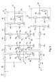
- Fig. 1 shows an overview block diagram of the inventive arrangement for level control of integrated amplifier units.
- the amplifier unit 1 is usually realized as an integrated component.
- This amplifier unit 1 can be produced, for example, by an MMIC process as an integrated amplifier unit.
- This includes a power amplifier 2 which may consist of several cascaded amplifier stages.
- the high-frequency signal, in the following HF signal 23, generated by the power amplifier 2 is fed to a detector element 3, which is connected to the output of the power amplifier 2.
- a reference element 4 and a device 5 for adjusting the bias voltages (bias) of the power amplifier 2 are located in the amplifier unit 1.
- the amplifier unit 1 comprises an input 6 to which the RF signal to be amplified is applied. Furthermore, the amplifier unit 1 comprises an input 7 to which the drain voltage 18 is applied. Via a further input 8, the operating point of the power amplifier 2 can be set. Via the input 9, the amplification factor of the power amplifier 2 can be set. Via the output 10, the RF signal 23 can be supplied to other devices. At the exit 11 is the Detector signal 13 of the detector element 3 on. At the output 12, the reference signal 14 of the reference element 4 is present.
- the temperature-dependent error of the detector signal 13 is compensated by means of the reference signal 14 by a differential amplifier 15.
- This differential amplifier 15 is constructed by analog modules such as operational amplifier.
- the output signal 16 of the differential amplifier 15 is passed to a first input of an adder 17.
- a current measuring element 19 the current consumption of the drain is measured.
- the current measuring element 19 may consist of a shunt resistor and / or of a Hall element.
- the measured current is transmitted via an in FIG. 1
- the weighted by the factor K current signal which now represents the error voltage by which the detector signal 13 of the detector element 3 deviates from the actual value
- a second input 25 of the adder 17 is supplied.
- the adder 17 is constructed in the embodiment with analog elements such as an operational amplifier.
- the output of the adder 17 is connected to the input of the regulator 22.
- a control voltage 24 is applied, which is dependent on, preferably proportional to the desired high-frequency level at the output 10 of the amplifier unit 1.
- the amplifier unit 1 can still have a separate input 30 to which a voltage can be applied, with which the reference element 4 is biased.
- the bias voltage for the reference element 4 is lowered via a voltage divider.
- This can lead to a higher accuracy in amplifier units 1, in which the reference signal 14 has a strong offset (offset voltage).
- offset voltage can be compensated in addition to a voltage divider, which lowers the bias of the reference element, also by means of a digital / analog converter, which is connected together with the drain voltage to a differential amplifier.
- the output of the differential amplifier is connected to the input 30.
- the amplifier unit 1 includes at least one amplifier stage 31 first
- the amplifier stage 31 1 includes two transistors 32 1 , 36 1 , which are interconnected complementary to each other.
- a first terminal 33 1 of a first transistor 32 1 is connected via the resistor 42 1 to the drain line.
- the resistors 41 1 , 42 1 and 45 1 represent parasitic line impedances that form on the leads to the transistors.
- the second terminal 34 1 of the first transistor 32 1 is connected to the input 9. About the control voltage applied to the input 9, the gain of the amplifier unit 1 can be adjusted.
- a third terminal 35 1 of the first transistor 32 1 is connected to the first terminal 37 1 of the second transistor 36 1 .
- the second port 38 1 of the second Transistor 36 1 is connected to the RF signal to be amplified.
- a third terminal 39 1 of the second transistor 36 1 is connected to the reference ground.
- FIG. 2 For example, two further amplifier stages are shown in order to better illustrate the mode of operation. The structure of these amplifier stages corresponds to the already described amplifier stage 31 1 . Only the indices 2 and n of the reference numerals differ in the amplifier stages.
- the resistors 40, 43, 44 also represent parasitic line impedances or serve to terminate the line.
- the drain resistor 57, over which the sum of the drain currents drops, is preferably outside the housing of the integrated circuit (IC), so that as little power is dissipated in the IC package.
- Via the input 8 can be applied via a voltage divider 46, 47, a control voltage to the source line, which is superimposed on the RF signal, which is applied to the input 6. Due to the DC component of the control voltage, the operating point of the transistors 36 1 , 36 2 , 36 n is set via the second terminal 38 1 , 38 2 , 38 n .
- the amplification factor of the amplifier stage 31 1 , 31 2 , 31 n is set via the input 9.
- the control voltage at the input 9 can be connected to another DC voltage in Fig. 2 not shown, are superimposed. This can happen, for example, via a voltage divider, not shown, to the drain line.
- the amplified RF signal is divided down before the output 10 and the anode the detector diode 55 is supplied.
- a capacitor 51 is connected to ground, in order to divert the alternating component to ground, so that at the output 11, a pure DC component is maintained.
- the resistors 48, 49, 50, the capacitor 51 and the detector diode 55 form the detector element 3.
- a further voltage divider 52, 53 divides a voltage at the input 30, which is usually connected to the input 7 of the drain line and supplies it to the anode of the reference diode 56.
- the output 12 and a resistor 54 connects to the reference ground.
- the resistors 52, 53, 54 and the reference diode 56 form the reference element 4.
- Other connection combinations are also conceivable.
- Fig. 3A shows the detection and preparation of the drain current.
- a drain voltage 18 is applied to the input 26.
- the input 26 is connected to the input 7 of the amplifier unit 1.
- the shunt resistor 60 may consist of a plurality of resistors connected in parallel with each other.
- the voltage before and after the shunt resistor 60 for example, via resistors 67, 68 fed to a differential amplifier operating amplifier 63.
- the differential amplifier can be connected by inserting the capacitor 64 in parallel with the resistor 66 in the Feedback to the low pass 1st order to be extended. However, the cutoff frequency of the filter must be below the lowest signal frequency to be amplified.
- the differential amplifier serves to amplify the signal in order subsequently to be able to set the desired weighting of the signal, for example by means of a potentiometer 65. Also done by the differential amplifier, an impedance matching. One terminal of the potentiometer 65 is preferably connected to the output of the differential amplifier. A second terminal of the potentiometer 65 is connected to the input 25 of an adder 17 (see Fig. 1 ) and a third terminal of the potentiometer 65 is connected to ground.
- the potentiometer 65 may be designed as a conventional potentiometer or as a digital potentiometer.
- Fig. 3B shows an advantageous development for the detection and preparation of the drain current.
- the drain current becomes as in Fig. 3A detected via at least one shunt resistor 60 and fed to a working as a differential amplifier operational amplifier 63.
- the output signal 72 is supplied to a first input of a second differential amplifier operating amplifier 70, for example via a resistor 75.
- the resistor 75 together with another resistor 76, forms a voltage divider.
- a digital / analog converter (D / A converter) 71 is connected to the second input of the operational amplifier 70 via a further resistor 74.
- the gradations in a D / A converter 71 are significantly finer.
- the voltage signal 72 weighted differently. This weighting can be adjusted during operation. This is the basis of Fig. 1 realized correction factor K realized.
- Fig. 4 shows a possible embodiment of the controller 22 according to the invention Fig. 1 ,
- the controller 22 is in Fig. 4 from an operational amplifier 84 operating as a differential amplifier 80 and an operational amplifier 87 operating as a proportionally integrated PI controller 81.
- the output signal 21 of the adder 17 is output to a first terminal 82 of the differential amplifier 80 Fig. 1 created via a resistor 90.
- the resistor 90 together with the resistor 91 forms a voltage divider.
- the differential amplifier 80 can be realized by inserting the capacitor 85 in parallel with the resistor 93 in the feedback as a low-pass 1st order.
- the output signal 86 is supplied to the PI controller 81.
- the PI controller 81 connected downstream via a resistor 94 includes an operational amplifier 87 in the feedback of which a resistor 95 and a capacitor 96 are connected in series so that the operational amplifier 87 operates as an integrator.
- the first entrance 89 of the Operational amplifier 87 is connected to ground.
- the manipulated variable 28, which is generated by the controller 22 and applied to the output, is delivered to the terminal 9.
- the differential amplifier 80 is dispensed with.
- the control voltage 24 for setpoint specification is connected to the first input 89 of the operational amplifier 87.
- the output signal 21 of the adder 17 off Fig. 1 is connected to the second input of the operational amplifier 87.
- Fig. 5A shows a further detailed embodiment of the present invention.
- Fig. 5A includes with the amplifier unit 1, the differential amplifier 15 and the current measuring element 19, the essential components already in Fig. 1 available.
- the controller 22 off Fig. 1 who in Fig. 4 is shown in detail, as well as the superimposition of the measured current value with a constant correction factor K, as well as the adder 17, which superimposes the corrected detector signal 16 with the corrected current signal, are replaced in this embodiment by a discrete-time rule computing device 100.
- the rule computing device 100 includes a microprocessor or advantageously a programmable logic device (FPGA).
- FPGA programmable logic device
- At least one analog / digital converter (A / D converter) 101, 102 and / or at least one digital / analog converter (D / A converter) 103, 104 is connected to the closed-loop control unit 100.
- the A / D converter or D / A converter may be devices having multiple input and output channels. However, it is preferable for each of the signals to be measured and for each size to be output a separate A / D converter or a separate D / A converter used.
- the A / D converters 101, 102 and the D / A converters 103, 104 may also be integrated in the rule computing device, eg in the microprocessor.
- the rule computing device 100 is advantageously connected to a higher-level control device via a digital interface 105, for example an SPI interface. Setpoint specifications for the level to be set can be specified via this digital interface 105.
- an analog control voltage 24 can also be supplied to the closed-loop control unit 100 as setpoint specification.
- the current consumption of the drain line of the amplifier unit 1 can take place via a current measuring element 19, as shown in FIG Fig. 3A is shown.
- the current measuring element 19 off Fig. 3A is then operated without the potentiometer, the output of the operational amplifier 63 is connected directly to the input of the A / D converter 101. It is important to ensure that the A / D converter is fully controlled over its entire measuring range in order to be able to use the entire resolution. For this purpose, the gain at the operational amplifier 63 via the resistors is set accordingly.
- this differential amplifier can also be replaced by a complete differential amplifier which outputs a differential voltage at the output.
- These two voltages will be applied to the A / D converter 101 which measures the voltage difference of the two input voltages determined.
- the reference signal 14 of the reference element 4 and the detector signal 13 of the detector element 3 are amplified by a differential amplifier 15 so far that the A / D converter 102 is fully controlled as possible and the whole resolution is available.
- the rule computing device 100 reads in the values of the A / D converters 101, 102 at constant intervals T A and calculates, based on a discrete-time model of the transmission path together with the predetermined desired value, the manipulated variables to be output.
- the A / D converters begin to detect the signals to be measured at the same time.
- the manipulated variables relate to the amplification factor and the operating point of the power amplifier 2.
- the manipulated variable for setting the operating point of the power amplifier 2 is transmitted to the D / A converter 103, which is connected to the input 8 of the amplifier unit 1.
- the manipulated variable for the amplification factor power amplifier 2 is transmitted to the D / A converter 104, which is connected to the input 9 of the amplifier unit 1.
- the closed-loop control unit 100 more complex controller structures can be realized in addition to a PI controller.
- a lookup table is implemented that includes a correction factor that must be added to the measured but erroneous detector voltage 13 to compensate for the measurement error caused by the voltage drop across the parasitic impedances.
- the control computing device 100 is still supplied with the operating frequency, for example via the digital interface 105.
- the set operating point and the amplification factor are known, so that the Correction factor can be read from the table (lookuptable).
- the lookup table is preferably created once and stored in non-volatile memory.
- Fig. 5B shows a further embodiment of the present invention.
- the reference signal 14 of the reference element 4 is supplied to an A / D converter 110 and the detector signal 13 of the detector element 3 to an A / D converter 111.
- Both signals 13, 14 can each be amplified by an operational amplifier, not shown, so that the entire resolution of the A / D converter 110, 111 can be used.
- the rule computing device 100 detects the detector signal 13 and the reference signal 14 separately. As a result, errors can be better recognized on the one hand and on the other hand, the discrete-time model of the transmission link can be optimized.
- the invention is not limited to the illustrated embodiments.
- the present invention is also applicable to a level control of amplifier units that can amplify more than one RF signal and have integrated detector elements.
- the invention is also applicable to a level control of amplifier units, which amplify a differential (symmetrical) signal instead of a mass-related (unbalanced) signal and thereby have integrated detector elements. All described and / or designated elements can be combined as desired within the scope of the invention.
- filters when using a discrete-time rule computing device all filters are also implemented as digital filters in discrete-time rule computing device.
- the cutoff frequency of the filter or even the filter type, or the controller depending on the load condition, operating frequency or user request can be changed during operation.
- the use of a discrete-time rule computing device in combination with an analog controller is also possible.
- the time-discrete regulating computer reads the actual values via an A / D converter and provides the analog controller with a setpoint via a D / A converter.
Abstract
Description
Die Erfindung betrifft eine Anordnung zur Pegelregelung integrierter Verstärkerbausteine, die in einem weiten Frequenzbereich betrieben werden.The invention relates to an arrangement for level control of integrated amplifier modules, which are operated in a wide frequency range.
Eine gattungsgemäße Anordnung zur Pegelregelung ist aus der
Der Erfindung liegt daher die Aufgabe zugrunde, eine stabile und genaue Pegelregelung über einen großen Frequenzbereich mit möglichst kostengünstigen Bauteilen zu schaffen, die auch für einen Verstärker in integrierter Bauweise geeignet ist.The invention is therefore an object of the invention to provide a stable and accurate level control over a large frequency range with low-cost components, which is also suitable for an amplifier in an integrated design.
Die Aufgabe wird durch die erfindungsgemäße Kompensationsschaltlung zur Pegelregelung integrierter Verstärkerbausteine mit den Merkmalen des Anspruchs 1 gelöst. Die Unteransprüche enthalten vorteilhafte Weiterbildungen der Erfindung.The object is achieved by the inventive compensation circuit for level control integrated amplifier modules with the features of
Die Erfindung eignet sich für integrierte Verstärkerbausteine, die in einem weiten Frequenzbereich von beispielsweise 30 kHz bis 40 GHz betrieben werden können und u.a. für Kommunikationssysteme und Mikrowellenanwendungen gedacht sind. Verstärkerbausteine mit diesen Eigenschaften verfügen über Transistoren mit hoher Elektronenbeweglichkeit und werden von verschiedenen Herstellern unter den Bezeichnungen HMET (High Electron Mobility Transistor) oder PHMET (Pseudomorphic High Electron Mobility Transistor) als integrierte Verstärkerbausteine, die u.a. in einem MMIC (Monolithic Microwave Integrated Circuit) Prozess hergestellt werden, angeboten. Die Verstärkereinheiten verfügen in der Regel über mehrere kaskadierte Verstärkerstufen.The invention is suitable for integrated amplifier modules, which can be operated in a wide frequency range of, for example, 30 kHz to 40 GHz and u.a. for communication systems and microwave applications. Amplifier devices with these characteristics have high electron mobility transistors and are used by various manufacturers under the designations HMET (High Electron Mobility Transistor) or PHMET (Pseudomorphic High Electron Mobility Transistor) as integrated amplifier devices, which i.a. offered in a MMIC (Monolithic Microwave Integrated Circuit) process. The amplifier units usually have several cascaded amplifier stages.
Zusätzlich umfassen die Verstärkereinheiten zumindest ein integriertes Detektorelement und bevorzugt zumindest ein integriertes Referenzelement, die bevorzugt aus zumindest einer Detektordiode und zumindest einer Referenzdiode bestehen. Das Detektorelement dient dabei zur Detektion der Ausgangsleistung der Verstärkereinheit. Das Referenzelement dient zur Kompensation des Temperaturgangs des Detektorelements, weil insbesondere die Detektordiode ein temperaturabhängiges Verhalten aufweist. Aufgrund der angestrebten hohen Bandbreite können Richtkoppler nicht wirtschaftlich eingesetzt werden, weil die benötigte Chipfläche signifikant zunehmen würde. Eine kapazitive Ankopplung der Detektordiode scheitert ebenfalls an der signifikanten Zunahme der benötigten Chipfläche, um die notwendige Koppelkapazität realisieren und integrieren zu können. Aus diesem Grund wird bei diesen Verstärkereinheiten das Detektorelement bevorzugt galvanisch mit Ausgangssignal der Verstärkereinheit verbunden. Das Detektorelement wird hierfür meistens mit der HF-führenden Leitung verbunden, die meist auch die Drain-Versorgungsspannung führt. Diese Verbindung kann über einen Spannungsteiler erfolgen. Die Vorspannung der Referenzdiode kann bei vielen Verstärkereinheiten separat zugeführt werden, bei einigen ist diese aber auch fest mit dem Drain am Eingang der Verstärkereinheit verbunden. Bei keinem der bekannten Verstärkereinheiten ist das Referenzelement allerdings an derselben Stelle des Drains angeschlossen wie das Detektorelement, weil es ohne Dämpfung des Ausgangssignals nicht ohne weiteres möglich ist, den Wechselanteil des Ausgangssignals von der Referenzdiode zu entkoppeln.In addition, the amplifier units comprise at least one integrated detector element and preferably at least one integrated reference element, which preferably consists of at least one detector diode and at least one reference diode. The detector element serves to detect the output power of the amplifier unit. The reference element serves to compensate the temperature response of the detector element, because in particular the detector diode has a temperature-dependent behavior. Due to the desired high bandwidth directional couplers can not be used economically, because the required chip area would increase significantly. A capacitive coupling of the detector diode also fails due to the significant increase in the required chip area in order to realize and integrate the necessary coupling capacity. For this reason, in these amplifier units, the detector element is preferably galvanically connected to the output signal of the amplifier unit. For this purpose, the detector element is usually connected to the RF-leading line, which usually also leads to the drain supply voltage. This connection can be made via a voltage divider. The bias of the reference diode can be separately supplied to many amplifier units, but in some it is also firmly connected to the drain at the input of the amplifier unit. In none of the known amplifier units, however, the reference element is connected at the same point of the drain as the detector element, because it is not readily possible without attenuation of the output signal to decouple the alternating component of the output signal from the reference diode.
Wird nun, wie in den meisten Verstärkereinheiten, die Referenzdiode mit der Drainspannung, wie sie am Eingang der Verstärkereinheit anliegt, vorgespannt, so unterscheidet sich die Vorspannung an der Referenzdiode von der Vorspannung an der Detektordiode je nach Lastzustand der Verstärkereinheit. Dies ist auf den Spannungsabfall auf der Drainleitung zurückzuführen, der durch das Ausbilden von parasitären Impedanzen auf den Bondleitungen und den Zuleitungen in der Verstärkereinheit hervorgerufen wird. Bei einem hohen Ausgangspegel der Verstärkereinheit steigt die Stromaufnahme der Verstärkereinheit über die Drainleitung an, was dazu führt, dass der Spannungsabfall über die parasitären Impedanzen auf der Drainleitung ebenfalls zunimmt und die Vorspannung der Detektordiode deutlich unter der von der Referenzdiode liegt.If, as in most amplifier units, the reference diode is biased with the drain voltage applied to the input of the amplifier unit, then the bias voltage at the reference diode differs from the bias voltage at the detector diode, depending on the load state of the amplifier unit. This is due to the voltage drop on the drain line caused by the formation of parasitic impedances on the bond lines and the leads in the amplifier unit is caused. At a high output level of the amplifier unit, the current consumption of the amplifier unit increases via the drain line, with the result that the voltage drop across the parasitic impedances on the drain line also increases and the bias voltage of the detector diode is significantly lower than that of the reference diode.
Die Vorspannung der Referenzdiode erfährt hingegen keinen merklichen Spannungsabfall, weil sie keine signifikante Stromaufnahme aufweist. Bei Verwendung eines bekannten Regelverfahrens, z.B. dem aus der
Dasselbe Problem ergibt sich im umgekehrten Fall, wenn die Ausgangsleistung erhöht werden soll. Dieses Problem wird noch verstärkt, wenn beide Dioden nicht in einem separaten Schottky-Prozess hergestellt werden. Die Dioden einiger Verstärkereinheiten scheinen durch einen Metall-Halbleiter-Feldeffekttransistor (MESFET) gebildet zu sein, dessen Leistungsfähigkeit unterhalb derer einer dedizierten Schottky-Diode liegt. Generell führt die angesprochene Problematik dazu, dass mit bekannten Verfahren keine der integrierten Detektordioden für eine genaue Pegelregelung nutzbar sind.The same problem arises in the reverse case when the output power is to be increased. This problem is compounded when both diodes are not manufactured in a separate Schottky process. The diodes of some amplifier units shine through a metal-semiconductor field-effect transistor (MESFET) whose performance is below that of a dedicated Schottky diode. In general, the problem addressed leads to the fact that with known methods none of the integrated detector diodes can be used for accurate level control.
Das Konzept der Erfindung beruht auf der Tatsache, dass bei allen untersuchten Verstärkereinheiten der Spannungsabfall weitestgehend linear zur Stromaufnahme am Drain-Eingang ist. In der vorliegenden Erfindung wird die Stromaufnahme am Draineingang der Verstärkereinheit über zumindest ein Strommessglied gemessen. Das Strommessglied umfasst dabei bevorzugt zumindest einen Shuntwiderstand oder zumindest ein Hallelement. Das Stromsignal selbst wird über einen Differenzverstärker verstärkt, wobei gleichzeitig auch eine Impedanzanpassung erfolgt. Das Ausgangssignal des Differenzverstärkers, das Stromsignal, wird mit einem Korrekturfaktor K überlagert bzw. mit diesem multipliziert. Der Korrekturfaktor K führt das gemessene Stromsignal in eine Fehlerspannung über, die zur Detektorspannung addiert werden muss, um dadurch den Spannungsabfall auf der Drainleitung zu kompensieren. Der Faktor K berücksichtigt neben der Höhe des Spannungsabfalls auch die Kennlinie der Detektordiode. Die Höhe des Spannungsabfalls ist, wie bereits dargelegt, von der Stromaufnahme, sowie von der Impedanz der Bondleitung und der Impedanz der Drainleitung abhängig und kann gemessen werden.The concept of the invention is based on the fact that in all examined amplifier units, the voltage drop is largely linear to the current consumption at the drain input. In the present invention, the current consumption at the drain input of the amplifier unit is measured via at least one current measuring element. The current measuring element preferably comprises at least one shunt resistor or at least one Hall element. The current signal itself is amplified by a differential amplifier, wherein at the same time an impedance matching takes place. The output signal of the differential amplifier, the current signal, is superimposed with a correction factor K or multiplied by this. The correction factor K converts the measured current signal into an error voltage which must be added to the detector voltage, thereby compensating for the voltage drop on the drain line. In addition to the magnitude of the voltage drop, the factor K also takes into account the characteristic curve of the detector diode. The magnitude of the voltage drop is, as already explained, dependent on the current consumption, as well as on the impedance of the bond line and the impedance of the drain line and can be measured.
Der Korrekturfaktor K kann z.B. durch einen Spannungsteiler, oder durch ein Potentiometer, oder durch einen Operationsverstärker oder durch einen Digital/Analog-Wandler eingestellt werden. Von der Ausgangsspannung der Detektordiode wird die Ausgangsspannung der Referenzdiode abgezogen. Dies geschieht z.B. mittels eines Differenzverstärkers. Dem Ausgangssignal dieses Differenzverstärkers wird die mit dem Faktor K gewichtete Fehlerspannung addiert. Dies geschieht durch einen weiteren Operationsverstärker. Das Ausgangssignal dieses weiteren Operationsverstärkers wird dem Eingang eines Reglers zugeführt. Der Regler kann als PI-Regler (proportional integral Regler) aufgebaut sein, wobei auch andere Reglerstrukturen möglich sind. Eine Sollwertvorgabe, in Form einer Steuerspannung, die abhängig vom, vorzugsweise proportional zum Ausgangspegel ist, wird ebenfalls dem Regler zugeführt. Der Regler kann durch analoge Elemente, wie z.B. Operationsverstärker oder durch zeitdiskret arbeitende Elemente, wie z.B. Mikroprozessoren oder FPGAs aufgebaut sein. Der Regler kann auch in einem Regelrechengerät implementiert sein.The correction factor K can be adjusted for example by a voltage divider, or by a potentiometer, or by an operational amplifier or by a digital / analog converter. Of the Output voltage of the detector diode, the output voltage of the reference diode is subtracted. This happens, for example, by means of a differential amplifier. The output signal of this differential amplifier is added to the factor K weighted error voltage. This is done by another operational amplifier. The output signal of this further operational amplifier is supplied to the input of a regulator. The controller can be constructed as PI controller (proportional integral controller), although other controller structures are possible. A setpoint input, in the form of a control voltage that is dependent on, preferably proportional to the output level, is also supplied to the controller. The controller can be constructed by analog elements, such as operational amplifiers or by discrete-time operating elements, such as microprocessors or FPGAs. The controller can also be implemented in a rule computing device.
Der Ausgang des Reglers ist mit zumindest einem Eingang der Verstärkereinheit verbunden, über den der Verstärkungsfaktor eingestellt werden kann. Die hierfür notwendige Regelgröße wird bevorzugt direkt vom Regler erzeugt. Die notwendige Regelgröße kann allerdings auch von einem Digital/Analog-Wandler, der mit dem Regelrechengerät verbunden ist, erzeugt werden. Die Regelgröße am Ausgang des Reglers ist nicht nur von dem Detektorsignal und dem Referenzsignal abhängig, sondern auch zusätzlich von der Stromaufnahme der Verstärkereinheit.The output of the regulator is connected to at least one input of the amplifier unit, via which the amplification factor can be set. The required control variable is preferably generated directly by the controller. However, the necessary controlled variable can also be generated by a digital / analog converter, which is connected to the rule computing device. The control variable at the output of the controller is not only dependent on the detector signal and the reference signal, but also in addition to the power consumption of the amplifier unit.
Ein bei manchen Verstärkereinheiten zusätzlicher Eingang zur Einstelllung des Arbeitspunktes ist bevorzugt über eine Steuergröße einstellbar. Diese Steuergröße kann in der ersten erfindungsgemäßen Ausführungsform als konstant betrachtet werden. In einer weiteren erfindungsgemäßen Ausführungsform kann diese Steuergröße durch einen Digital/Analog-Wandler, der mit einem zeitdiskret arbeitenden Regelrechengerät verbunden ist, bereit gestellt werden. An das Regelrechengerät können zumindest zwei Analog/Digital-Wandler angeschlossen werden, über die zum einen die Stromaufnahme der Verstärkereinheit und zum anderen der um die Temperaturdrift kompensierte Ausgangspegel digital gemessen werden. An das Regelrechengerät sind bevorzugt ebenfalls zumindest zwei Digital/Analog-Wandler angeschlossen, die zwei Regelgrößen ausgeben, über die zum einen der Arbeitspunkt und zum anderen der Verstärkungsfaktor der Verstärkereinheit eingestellt werden kann. Das Regelrechengerät selbst ist dabei vorzugsweise mit einem übergeordneten Steuersystem verbunden. Sollwertvorgaben werden von diesem übergeordneten Steuersystem empfangen und Messgrößen werden an das übergeordnete Steuersystem übertragen.An additional input for adjusting the operating point in some amplifier units is preferably adjustable via a control variable. This control quantity can be considered constant in the first embodiment according to the invention to be viewed as. In a further embodiment according to the invention, this control variable can be provided by a digital / analogue converter which is connected to a time-discrepant regulating computing device. At least two analog / digital converters can be connected to the control computing device, via which the power consumption of the amplifier unit and the output level compensated for the temperature drift are measured digitally. At least two digital / analog converters are preferably also connected to the control computing device, which output two control variables via which the operating point and the amplification factor of the amplifier unit can be set on the one hand. The rule computing device itself is preferably connected to a higher-level control system. Setpoint specifications are received by this higher-level control system and measured variables are transmitted to the higher-level control system.
Durch diese erfindungsgemäße Kompensation wird eine unerwünschte Mitkopplung über eine Modulation der Vorspannung der Detektordiode mit dem Hochfrequenzsignal vermieden und die Regelung wird stabil in Gegenkopplung betrieben. Die Regelung ist weiterhin geeignet, um sehr schnell und genau einen gewünschten Ausgangspegel bei einer gewünschten Frequenz für interne Signalquellen einzustellen. Weiterhin kann durch Nutzung des internen Detektorelements auf den Einsatz von externen breitbandigen Kopplern und zusätzlichen Leistungsdetektoren verzichtet werden. Dadurch verbessert sich zusätzlich das Rauschverhalten gegenüber bekannten Lösungen. Messungen haben gezeigt, dass ohne die Erfassung und Rückführung des Drainstroms eine Pegelabweichung von bis zu +/- 5 dB, je nach Eingangsleistung, gegenüber dem Sollwert auftritt. Unter Verwendung der Pegelregelung gemäß vorliegender Erfindung liegt die Pegelabweichung bei unter +/- 0,3 dB gegenüber dem vorgegebenen Sollwert.By means of this compensation according to the invention, unwanted positive feedback via a modulation of the bias voltage of the detector diode with the high-frequency signal is avoided and the regulation is operated stably in negative feedback. The control is also suitable for setting very quickly and accurately a desired output level at a desired frequency for internal signal sources. Furthermore, by using the internal detector element can be dispensed with the use of external broadband couplers and additional power detectors. This additionally improves the noise behavior compared to known solutions. Measurements have shown that without the detection and feedback of the drain current, a level deviation of up to +/- 5 dB, depending on the input power, over the Setpoint occurs. Using the level control of the present invention, the level deviation is less than +/- 0.3 dB from the predetermined set point.
Verschiedene Ausführungsbeispiele der Erfindung werden nachfolgend unter Bezugnahme auf die Zeichnung beispielhaft beschrieben. Gleiche Gegenstände weisen dieselben Bezugszeichen auf. Die entsprechenden Figuren der Zeichnung zeigen im Einzelnen:
- Fig. 1
- ein Blockschaltbild eines erfindungsgemäßen Ausführungsbeispiels, das eine Gesamtübersicht der erfindungsgemäßen Anordnung zur Pegelregelung integrierter Verstärkereinheiten beinhaltet;
- Fig. 2
- einen schematischen Aufbau der Verstärkereinheit eines erfindungsgemäßen Ausführungsbeispiels mit verschiedenen Verstärkerstufen und dem Anschluss der Detektordiode und der Referenzdiode, wie er in unterschiedlichen integrierten Verstärkereinheiten realisiert sein kann;
- Fig. 3A
- eine Erfassung und Aufbereitung des Drainstroms gemäß eines erfindungsgemäßen Ausführungsbeispiels;
- Fig. 3B
- eine weiteres Ausführungsbeispiel zur Erfassung und Aufbereitung des Drainstroms gemäß der Erfindung;
- Fig. 4
- ein Ausführungsbeispiel eines PI-Reglers gemäß eines erfindungsgemäßen Ausführungsbeispiels;
- Fig. 5A
- ein Ausführungsbeispiel unter Verwendung eines zeitdiskret arbeitenden Regelrechengerätes gemäß der Erfindung und
- Fig. 5B
- ein weiteres Ausführungsbeispiel unter Verwendung eines zeitdiskret arbeitenden Regelrechengerätes gemäß der Erfindung.
- Fig. 1
- a block diagram of an embodiment of the invention, which includes an overall view of the inventive arrangement for level control integrated amplifier units;
- Fig. 2
- a schematic structure of the amplifier unit of an embodiment according to the invention with different amplifier stages and the connection of the detector diode and the reference diode, as it can be implemented in different integrated amplifier units;
- Fig. 3A
- a detection and processing of the drain current according to an embodiment of the invention;
- Fig. 3B
- a further embodiment for the detection and preparation of the drain current according to the invention;
- Fig. 4
- an embodiment of a PI controller according to an embodiment of the invention;
- Fig. 5A
- an embodiment using a discrete-time rule rule computing device according to the invention and
- Fig. 5B
- a further embodiment using a discrete-time rule rule computing device according to the invention.
Die Verstärkereinheit 1 umfasst einen Eingang 6, an dem das zu verstärkende HF-Signal angelegt wird. Weiterhin umfasst die Verstärkereinheit 1 einen Eingang 7 an den die Drainspannung 18 angelegt wird. Über einen weiteren Eingang 8 kann der Arbeitspunkt des Leistungsverstärkers 2 eingestellt werden. Über den Eingang 9 kann der Verstärkungsfaktor des Leistungsverstärkers 2 eingestellt werden. Über den Ausgang 10 kann das HF-Signal 23 weiteren Einrichtungen zugeführt werden. Am Ausgang 11 liegt das Detektorsignal 13 des Detektorelements 3 an. Am Ausgang 12 liegt das Referenzsignal 14 des Referenzelements 4 an.The
Der temperaturabhängige Fehler des Detektorsignals 13 wird mittels des Referenzsignals 14 durch einen Differenzverstärker 15 kompensiert. Dieser Differenzverstärker 15 ist durch analoge Bausteine wie z.B. Operationsverstärker aufgebaut. Das Ausgangssignal 16 des Differenzverstärkers 15 wird auf einen ersten Eingang eines Addierers 17 geleitet. Über ein Strommessglied 19 wird die Stromaufnahme des Drains gemessen. Das Strommessglied 19 kann aus einem Shuntwiderstand und/oder aus einem Hallelement bestehen. Der gemessene Strom wird über einen in
Der Ausgang des Addierers 17 wird mit dem Eingang des Reglers 22 verbunden. An einen zweiten Eingang des Reglers 22 wird eine Steuerspannung 24 angelegt, die abhängig vom, vorzugsweise proportional zum gewünschten Hochfrequenz-Pegel am Ausgang 10 der Verstärkereinheit 1 ist. Die Verstärkereinheit 1 kann noch einen separaten Eingang 30 aufweisen, an welchen eine Spannung angelegt werden kann, mit der das Referenzelement 4 vorgespannt wird.The output of the
In einer weiteren Ausführungsform der vorliegenden Erfindung wird die Vorspannung für das Referenzelement 4 über einen Spannungsteiler abgesenkt. Dies kann bei Verstärkereinheiten 1, bei denen das Referenzsignal 14 mit einem starken Offset (Versatz-Spannung) behaftet ist, zu einer höheren Genauigkeit führen. Ein solcher Offset kann neben einem Spannungsteiler, der die Vorspannung des Referenzelements senkt, auch mittels eines Digital/Analog-Wandlers, der zusammen mit der Drainspannung mit einem Differenzverstärkers verbunden ist, kompensiert werden. Hierzu wird der Ausgang des Differenzverstärkers mit dem Eingang 30 verbunden.In a further embodiment of the present invention, the bias voltage for the reference element 4 is lowered via a voltage divider. This can lead to a higher accuracy in
Ein dritter Anschluss 351 des ersten Transistors 321 ist mit dem ersten Anschluss 371 des zweiten Transistors 361 verbunden. Der zweite Anschluss 381 des zweiten Transistors 361 ist dem zu verstärkenden HF-Signal verbunden. Ein dritter Anschluss 391 des zweiten Transistors 361 ist mit der Bezugsmasse verbunden. Neben der ersten Verstärkerstufe 311 kann es noch weitere Verstärkerstufen geben. In
Über den Eingang 8 kann über einen Spannungsteiler 46, 47 eine Steuerspannung an die Sourceleitung angelegt werden, die sich mit dem HF-Signal, das am Eingang 6 angelegt wird, überlagert. Durch den Gleichanteil der Steuerspannung wird der Arbeitspunkt der Transistoren 361, 362, 36n über den zweiten Anschluss 381, 382, 38n eingestellt. Der Verstärkungsfaktor der Verstärkerstufe 311, 312, 31n wird über den Eingang 9 eingestellt. Die Steuerspannung am Eingang 9 kann mit einer weiteren Gleichspannung, die in
Über einen Spannungsteiler 48, 49 wird das verstärkte HF-Signal vor dem Ausgang 10 herunter geteilt und der Anode der Detektordiode 55 zugeführt. An der Kathode der Detektordiode 55 schließt sich neben einem Widerstand 50 auch ein Kondensator 51 gegen Masse an, um den Wechselanteil gegen Masse abzuleiten, so dass am Ausgang 11 ein reiner Gleichanteil erhalten bleibt. Die Widerstände 48, 49, 50, der Kondensator 51 und die Detektordiode 55 bilden das Detektorelement 3.Via a
Ein weiterer Spannungsteiler 52, 53 teilt eine Spannung am Eingang 30 herunter, welcher meistens mit dem Eingang 7 der Drainleitung verbunden ist und führt diese der Anode der Referenzdiode 56 zu. An die Kathode der Referenzdiode 56 schließt sich der Ausgang 12 und ein Widerstand 54 gegen die Bezugsmasse an. Die Widerstände 52, 53, 54 und die Referenzdiode 56 bilden das Referenzelement 4.A
In einer weiteren Ausführungsform der vorliegenden Erfindung ist der erste Anschluss 331, 332, 33n, 371, 372, 37n der Transistoren 321, 322, 32n, 361, 362, 36n mit dem Drain, ein zweiter Anschluss 341, 342, 34n, 381, 382, 38n der Transistoren 321, 322, 32n, 361, 362, 36n mit dem Gate und ein dritter Anschluss 351, 352, 35n, 391, 392, 39n der Transistoren 321, 322, 32n, 361, 362, 36n mit dem Source verbunden. Andere Anschlusskombinationen sind ebenfalls denkbar.In a further embodiment of the present invention, the
Anhand von
Sollten die Verstärkerstufen 311, 322, 32n der Verstärkereinheit 1 über den Ausgang 10 der Verstärkereinheit 1 mit einer konstanten Drainspannung versorgt werden, so würde ebenfalls ein Spannungsabfall über dem Bondwiderstand 58 dazu führen, dass sich die Vorspannung der Detektordiode 55 von der Vorspannung der Referenzdiode 56 unterscheidet, was die Verwendung der hier vorliegenden Erfindung ebenfalls unabdingbar macht.If the amplifier stages 31 1 , 32 2 , 32 n of the
Der Differenzverstärker dient dazu, das Signal zu verstärken, um anschließend die gewünschte Gewichtung des Signals z.B. durch ein Potentiometer 65 einstellen zu können. Ebenfalls erfolgt durch den Differenzverstärker eine Impedanzanpassung. Ein Anschluss des Potentiometers 65 wird bevorzugt mit dem Ausgang des Differenzverstärkers verbunden. Ein zweiter Anschluss des Potentiometers 65 wird mit dem Eingang 25 eines Addierers 17 (siehe
Der Differenzverstärker 80 kann durch Einfügen der Kapazität 85 parallel zum Widerstand 93 in der Rückkopplung als Tiefpass 1. Ordnung realisiert werden. Das Ausgangssignal 86 wird dem PI-Regler 81 zugeführt. Der über eine Widerstand 94 nachgeschaltete PI-Regler 81 beinhaltet einen Operationsverstärker 87, in dessen Rückführung ein Widerstand 95 und ein Kondensator 96 in Reihe geschaltet sind, so dass der Operationsverstärker 87 als Integrierer arbeitet. Der erste Eingang 89 des Operationsverstärkers 87 wird mit Masse verbunden. Die Stellgröße 28, die vom Regler 22 erzeugt wird und am Ausgang anliegt, wird an dem Anschluss 9 abgegeben.The
In einer weiteren Ausführungsform der vorliegenden Erfindung wird auf den Differenzverstärker 80 verzichtet. Die Steuerspannung 24 zur Sollwertvorgabe wird mit dem ersten Eingang 89 des Operationsverstärkers 87 verbunden. Das Ausgangssignal 21 des Addierers 17 aus
Über diese digitale Schnittstelle 105 können Sollwertvorgaben für den einzustellenden Pegel vorgegeben werden.
Setpoint specifications for the level to be set can be specified via this
Es können aber auch die gemessenen Werte der A/D-Wandler an das übergeordnete Steuergerät übertragen werden. Über einen nicht dargestellten optionalen A/D-Wandler kann auch eine analoge Steuerspannung 24 als Sollwertvorgabe dem Regelrechengerät 100 zugeführt werden. Die Stromaufnahme der Drainleitung der Verstärkereinheit 1 kann über ein Strommessglied 19 erfolgen, wie es in
In einer weiteren Ausführungsform kann dieser Differenzverstärker auch durch einen vollständigen Differenzverstärker ersetzt werden, der am Ausgang eine differentielle Spannung ausgibt. Diese beiden Spannungen werden dem A/D-Wandler 101 zugeführt werden, der die Spannungsdifferenz der beiden Eingangsspannungen ermittelt. Das Referenzsignal 14 des Referenzelements 4 und das Detektorsignal 13 des Detektorelements 3 werden durch einen Differenzverstärker 15 soweit verstärkt, dass der A/D-Wandler 102 möglichst voll ausgesteuert ist und die ganze Auflösung nutzbar ist. Das Regelrechengerät 100 liest in konstanten Intervallen TA die Werte der A/D-Wandler 101, 102 ein und berechnet anhand eines zeitdiskreten Modells der Übertragungsstrecke zusammen mit dem vorgegebenen Sollwert die auszugebenenden Stellgrößen.In a further embodiment, this differential amplifier can also be replaced by a complete differential amplifier which outputs a differential voltage at the output. These two voltages will be applied to the A /
Die A/D-Wandler beginnen im selben Zeitpunkt die zu messenden Signale zu erfassen. Die Stellgrößen beziehen sich auf den Verstärkungsfaktor und den Arbeitspunkt des Leistungsverstärkers 2. Die Stellgröße für die Einstellung des Arbeitspunktes des Leistungsverstärkers 2 wird an den D/A-Wandler 103 übermittelt, der mit dem Eingang 8 der Verstärkereinheit 1 verbunden ist. Die Stellgröße für den Verstärkungsfaktor Leistungsverstärkers 2 wird an den D/A-Wandler 104 übermittelt, der mit dem Eingang 9 der Verstärkereinheit 1 verbunden ist. In dem Regelrechengerät 100 können neben einem PI-Regler auch komplexere Reglerstrukturen realisiert werden.The A / D converters begin to detect the signals to be measured at the same time. The manipulated variables relate to the amplification factor and the operating point of the
In einer weiteren Ausführungsform der vorliegenden Erfindung wird eine Tabelle (Lookuptable) implementiert, die einen Korrekturfaktor enthält, der zur gemessenen aber fehlerbehafteten Detektorspannung 13 addiert werden muss, um den Messfehler, der durch den Spannungsabfall an den parasitären Impedanzen hervorgerufen wird, zu kompensieren. Hierzu wird dem Regelrechengerät 100 noch die Betriebsfrequenz z.B. über die digitale Schnittstelle 105 zugeführt. Der eingestellte Arbeitspunkt und der Verstärkungsfaktor sind bekannt, so dass der Korrekturfaktor aus der Tabelle(Lookuptable) ausgelesen werden kann. Die Tabelle (Lookuptable) wird vorzugsweise einmalig erstellt und in einem nicht flüchtigen Speicher gespeichert.In another embodiment of the present invention, a lookup table is implemented that includes a correction factor that must be added to the measured but
Die Erfindung ist nicht auf die dargestellten Ausführungsbeispiele begrenzt. Die vorliegende Erfindung ist auch für eine Pegelregelung von Verstärkereinheiten anwendbar, die mehr als ein HF-Signal verstärken können und über integrierte Detektorelemente verfügen. Weiterhin ist die Erfindung ebenfalls für eine Pegelregelung von Verstärkereinheiten anwendbar, die statt einem massebezogenen (unsymmetrischen) Signal ein differentielles (symmetrisches) Signal verstärken und dabei über integrierte Detektorelemente verfügen. Alle beschriebenen und/oder bezeichneten Elemente sind im Rahmen der Erfindung beliebig miteinander kombinierbar.The invention is not limited to the illustrated embodiments. The present invention is also applicable to a level control of amplifier units that can amplify more than one RF signal and have integrated detector elements. Furthermore, the invention is also applicable to a level control of amplifier units, which amplify a differential (symmetrical) signal instead of a mass-related (unbalanced) signal and thereby have integrated detector elements. All described and / or designated elements can be combined as desired within the scope of the invention.
In einem weiteren nicht dargestellten Ausführungsbeispiel der vorliegenden Erfindung können bei Verwendung eines zeitdiskreten Regelrechengerätes sämtliche Filter auch als digitale Filter im zeitdiskreten Regelrechengerät implementiert werden. Dies betrifft unter anderem die Filter, die den A/D-Wandlern vorgeschalten sind. Dadurch ist es möglich, den analogen Teil auf wenige Komponenten zu beschränken, wohingegen der digitale Teil des Regelsystems, der neben der Filterstruktur auch die Reglerstruktur umfasst, je nach Anwendungsfall angepasst werden kann. So kann die Grenzfrequenz des Filters oder gar der Filtertyp, bzw. der Regler je nach Lastzustand, Betriebsfrequenz oder Benutzerwunsch im laufenden Betrieb gewechselt werden.In a further embodiment, not shown, of the present invention, when using a discrete-time rule computing device all filters are also implemented as digital filters in discrete-time rule computing device. This concerns, among other things, the filters that are upstream of the A / D converters. This makes it possible to restrict the analog part to a few components, whereas the digital part of the control system, which includes the filter structure and the controller structure, can be adapted depending on the application. Thus, the cutoff frequency of the filter or even the filter type, or the controller depending on the load condition, operating frequency or user request can be changed during operation.
Der Einsatz eines zeitdiskret arbeitenden Regelrechengeräts in Kombination mit einem analogen Regler ist ebenfalls möglich. Das zeitdiskret arbeitende Regelrechengerät liest über einen A/D-Wandler die IstWerte ein und gibt dem analogen Regler über einen D/A-Wandler einen Sollwert vor.The use of a discrete-time rule computing device in combination with an analog controller is also possible. The time-discrete regulating computer reads the actual values via an A / D converter and provides the analog controller with a setpoint via a D / A converter.
In einem weiteren nicht dargestellten Ausführungsbeispiel der vorliegenden Erfindung ist auch eine direkte Steuerung der A/D-Wandler und D/A-Wandler durch das übergeordnete Steuergerät möglich.In a further embodiment, not shown, of the present invention, a direct control of the A / D converter and D / A converter by the higher-level control unit is possible.
Claims (13)
dadurch gekennzeichnet,
dass die Regelgröße (28) zusätzlich von der Stromaufnahme der Verstärkereinheit (1) abhängig ist.Compensation circuit for a level control with an amplifier unit (1), wherein the amplifier unit (1) at least one amplifier stage (31 1 ) and at least one detector element (3) for detecting the output power of the amplifier unit (1) and a gain of the amplifier unit (1) via a control variable (28) is adjustable, which is dependent on a detector signal (13), which is generated by the detector element (3)
characterized,
that the controlled variable (28) additionally on the power consumption of the amplifier unit (1) is dependent.
dadurch gekennzeichnet,
dass die Verstärkereinheit (1) weiterhin ein Referenzelement (4) umfasst, welches das temperaturabhängige Verhalten des Detektorelements (3) kompensiert.Compensation circuit according to claim 1,
characterized,
that the amplifier unit (1) further comprises a reference element (4), which compensates for the temperature-dependent behavior of the detector element (3).
dadurch gekennzeichnet,
dass das Detektorelement (3) zumindest eine Detektordiode (55) umfasst.Compensation circuit according to claim 1 or 2,
characterized,
in that the detector element (3) comprises at least one detector diode (55).
dadurch gekennzeichnet,
dass das Referenzelement (4) zumindest eine Referenzdiode (56) umfasst.Compensation circuit according to claim 2,
characterized,
in that the reference element (4) comprises at least one reference diode (56).
dadurch gekennzeichnet,
dass ein Arbeitspunkt der Verstärkereinheit (1) über eine Steuergröße (27) einstellbar ist.Compensation circuit according to one of claims 1 to 4,
characterized,
that an operating point of the amplifier unit (1) via a control variable (27) is adjustable.
dadurch gekennzeichnet,
dass das Detektorelement (3) galvanisch mit einer Ausgangsleitung der Verstärkereinheit (1) verbunden ist.Compensation circuit according to one of claims 1 to 5,
characterized,
that the detector element (3) is electrically connected to an output line of the amplifier unit (1).
dadurch gekennzeichnet,
die Stromaufnahme der Verstärkereinheit (1) über zumindest ein Strommessglied (19) messbar ist.Compensation circuit according to one of claims 1 to 6,
characterized,
the current consumption of the amplifier unit (1) via at least one current measuring element (19) is measurable.
dadurch gekennzeichnet,
dass das Strommessglied (19) zumindest einen Shuntwiderstand (60) und/oder zumindest ein Hallelement umfasst.Compensation circuit according to claim 7,
characterized,
that the current measuring element (19) comprises at least one shunt resistor (60) and / or at least one Hall element.
dadurch gekennzeichnet,
dass ein von dem Strommessglied (19) gemessenes Stromsignal mit einem Korrekturfaktor (K) multipliziert ist.Compensation circuit according to claim 7 or 8,
characterized,
in that a current signal measured by the current measuring element (19) is multiplied by a correction factor (K).
dadurch gekennzeichnet,
dass der Korrekturfaktor (K) über zumindest einen Operationsverstärker (63) und/oder einen Spannungsteiler (65) und/oder einen Digital/Analog-Wandler (71) einstellbar ist.Compensation circuit according to claim 9,
characterized,
that the correction factor (K) via at least one operational amplifier (63) and / or a voltage divider (65) and / or a digital / analog converter (71) is adjustable.
dadurch gekennzeichnet,
dass die Regelgröße (28) von einem Regler (22) erzeugt wird.Compensation circuit according to claim 10,
characterized,
that the controlled variable (28) is generated by a controller (22).
dadurch gekennzeichnet,
dass der Regler (22) mit analogen Elementen oder mit zeitdiskreten Elementen aufgebaut ist.Compensation circuit according to claim 11,
characterized,
that the controller (22) is built with analogue elements or with time-discrete elements.
dadurch gekennzeichnet,
dass der Regler (22) in einem Regelrechengerät (100) implementiert ist, an das zumindest ein Analog/DigitalWandler (101, 102) und/oder zumindest ein Digital/AnalogWandler (103, 104) angeschlossen ist.Compensation circuit according to claim 11 or 12,
characterized,
in that the controller (22) is implemented in a control computing device (100) to which at least one analog / digital converter (101, 102) and / or at least one digital / analog converter (103, 104) is connected.
Applications Claiming Priority (1)
| Application Number | Priority Date | Filing Date | Title |
|---|---|---|---|
| DE102009050491A DE102009050491A1 (en) | 2009-10-23 | 2009-10-23 | Compensation circuit for improving the level control of integrated amplifier modules |
Publications (4)
| Publication Number | Publication Date |
|---|---|
| EP2315352A2 true EP2315352A2 (en) | 2011-04-27 |
| EP2315352A3 EP2315352A3 (en) | 2014-04-16 |
| EP2315352B1 EP2315352B1 (en) | 2020-11-25 |
| EP2315352B8 EP2315352B8 (en) | 2020-12-30 |
Family
ID=43502539
Family Applications (1)
| Application Number | Title | Priority Date | Filing Date |
|---|---|---|---|
| EP10013499.8A Active EP2315352B8 (en) | 2009-10-23 | 2010-10-11 | Compensation circuit for improving the level regulation of integrated amplifier components |
Country Status (2)
| Country | Link |
|---|---|
| EP (1) | EP2315352B8 (en) |
| DE (1) | DE102009050491A1 (en) |
Citations (1)
| Publication number | Priority date | Publication date | Assignee | Title |
|---|---|---|---|---|
| EP0834987A2 (en) | 1996-10-01 | 1998-04-08 | Nokia Mobile Phones Ltd. | A diode detector |
Family Cites Families (9)
| Publication number | Priority date | Publication date | Assignee | Title |
|---|---|---|---|---|
| US4523155A (en) * | 1983-05-04 | 1985-06-11 | Motorola, Inc. | Temperature compensated automatic output control circuitry for RF signal power amplifiers with wide dynamic range |
| TW225619B (en) * | 1991-07-19 | 1994-06-21 | Nippon Electric Co | |
| AU3985399A (en) * | 1998-05-18 | 1999-12-06 | Omnipoint Corporation | Amplifier with dynamically adaptable supply current |
| US6430402B1 (en) * | 1998-09-14 | 2002-08-06 | Conexant Systems, Inc. | Power amplifier saturation prevention method, apparatus, and communication system incorporating the same |
| US6580318B2 (en) * | 2001-03-08 | 2003-06-17 | Maxim Integrated Products, Inc. | Method and apparatus for protecting radio frequency power amplifiers |
| US7062237B2 (en) * | 2001-06-05 | 2006-06-13 | Telefonaktiebolaget Lm Ericsson (Publ) | Power amplifier (PA) with improved power regulation |
| US7433658B1 (en) * | 2003-09-30 | 2008-10-07 | Marvell International Ltd. | System and method for controlling true output power of a transmitter |
| DE602005000685T2 (en) * | 2004-01-21 | 2008-01-24 | Nec Corp. | Device and method for transmission power control, computer program for transmission power control device and radio transmitter |
| JP4488309B2 (en) * | 2005-02-28 | 2010-06-23 | 株式会社ルネサステクノロジ | Electronic components for high frequency power amplification |
-
2009
- 2009-10-23 DE DE102009050491A patent/DE102009050491A1/en not_active Withdrawn
-
2010
- 2010-10-11 EP EP10013499.8A patent/EP2315352B8/en active Active
Patent Citations (1)
| Publication number | Priority date | Publication date | Assignee | Title |
|---|---|---|---|---|
| EP0834987A2 (en) | 1996-10-01 | 1998-04-08 | Nokia Mobile Phones Ltd. | A diode detector |
Also Published As
| Publication number | Publication date |
|---|---|
| EP2315352A3 (en) | 2014-04-16 |
| DE102009050491A1 (en) | 2011-04-28 |
| EP2315352B1 (en) | 2020-11-25 |
| EP2315352B8 (en) | 2020-12-30 |
Similar Documents
| Publication | Publication Date | Title |
|---|---|---|
| DE19723645B4 (en) | Arrangement for signal transmission between a donor site and a receiving site | |
| DE112012002932B4 (en) | Current sensor with a calibration for a current divider configuration | |
| DE102012100144B4 (en) | Calibration circuit and method for calibrating capacitive compensation in digital-to-analog converters | |
| DE102015204519B4 (en) | Accurate current detection circuit and method for accurate current detection | |
| DE10223767A1 (en) | Circuit arrangement for processing a signal from a sensor | |
| EP2597931A2 (en) | Driver circuit and corresponding error recognition circuit and method for same | |
| DE102015204518B4 (en) | Offset compensation for a VDS compensator in a current detection circuit | |
| EP3030862B1 (en) | Circuit arrangement and method for controlling a displacement measurement sensor | |
| DE102018201310B4 (en) | Current sensor and circuit breaker | |
| DE102014202634A1 (en) | Current detection device and method for detecting an electric current | |
| DE602004003958T2 (en) | INTEGRATED POWER AMPLIFIER CIRCUIT | |
| DE102014004098B4 (en) | VIENNA BRIDGE OSCILLATOR AND CIRCUIT ARRANGEMENT FOR REGULATING DETERMINATION | |
| WO2014127960A1 (en) | Power measuring instrument with internal calibration of diode detectors | |
| EP3141878B1 (en) | Device and method for operating passive infrared sensors | |
| EP2315352B1 (en) | Compensation circuit for improving the level regulation of integrated amplifier components | |
| EP1067473B1 (en) | Integrator | |
| DE112021001588T5 (en) | CHOPPER-STABILIZED ATTENUATION FOR MEASURING AMPLIFIERS | |
| WO2016206934A1 (en) | Calibratable multiphase direct current transformer | |
| EP0456168A2 (en) | Device for the analogue-digital conversion of a measured quantity, generated by transducers disposed in a bridge circuit, in particular by gauges in a weighing cell | |
| WO2015113672A1 (en) | Semiconductor switch and method for determining a current through a semiconductor switch | |
| DE102021132537B3 (en) | CURRENT MEASUREMENT CIRCUIT | |
| EP1247109B1 (en) | Electrical circuit arrangement for converting an electrical input variable into an output electrical voltage | |
| EP0728297B1 (en) | Circuit assembly for the control of signals | |
| DE102022100125A1 (en) | DIAGNOSIS OF ELECTRICAL FAULTS IN CAPACITIVE SENSORS | |
| DE102022204429A1 (en) | Systems and methods for measuring delays between signals |
Legal Events
| Date | Code | Title | Description |
|---|---|---|---|
| PUAI | Public reference made under article 153(3) epc to a published international application that has entered the european phase |
Free format text: ORIGINAL CODE: 0009012 |
|
| AK | Designated contracting states |
Kind code of ref document: A2 Designated state(s): AL AT BE BG CH CY CZ DE DK EE ES FI FR GB GR HR HU IE IS IT LI LT LU LV MC MK MT NL NO PL PT RO RS SE SI SK SM TR |
|
| AX | Request for extension of the european patent |
Extension state: BA ME |
|
| PUAL | Search report despatched |
Free format text: ORIGINAL CODE: 0009013 |
|
| AK | Designated contracting states |
Kind code of ref document: A3 Designated state(s): AL AT BE BG CH CY CZ DE DK EE ES FI FR GB GR HR HU IE IS IT LI LT LU LV MC MK MT NL NO PL PT RO RS SE SI SK SM TR |
|
| AX | Request for extension of the european patent |
Extension state: BA ME |
|
| RIC1 | Information provided on ipc code assigned before grant |
Ipc: H03G 3/30 20060101AFI20140312BHEP |
|
| 17P | Request for examination filed |
Effective date: 20140417 |
|
| RBV | Designated contracting states (corrected) |
Designated state(s): AL AT BE BG CH CY CZ DE DK EE ES FI FR GB GR HR HU IE IS IT LI LT LU LV MC MK MT NL NO PL PT RO RS SE SI SK SM TR |
|
| 17Q | First examination report despatched |
Effective date: 20160506 |
|
| STAA | Information on the status of an ep patent application or granted ep patent |
Free format text: STATUS: EXAMINATION IS IN PROGRESS |
|
| GRAP | Despatch of communication of intention to grant a patent |
Free format text: ORIGINAL CODE: EPIDOSNIGR1 |
|
| STAA | Information on the status of an ep patent application or granted ep patent |
Free format text: STATUS: GRANT OF PATENT IS INTENDED |
|
| INTG | Intention to grant announced |
Effective date: 20200728 |
|
| GRAS | Grant fee paid |
Free format text: ORIGINAL CODE: EPIDOSNIGR3 |
|
| GRAA | (expected) grant |
Free format text: ORIGINAL CODE: 0009210 |
|
| STAA | Information on the status of an ep patent application or granted ep patent |
Free format text: STATUS: THE PATENT HAS BEEN GRANTED |
|
| AK | Designated contracting states |
Kind code of ref document: B1 Designated state(s): AL AT BE BG CH CY CZ DE DK EE ES FI FR GB GR HR HU IE IS IT LI LT LU LV MC MK MT NL NO PL PT RO RS SE SI SK SM TR |
|
| REG | Reference to a national code |
Ref country code: GB Ref legal event code: FG4D Free format text: NOT ENGLISH |
|
| REG | Reference to a national code |
Ref country code: DE Ref legal event code: R096 Ref document number: 502010016804 Country of ref document: DE |
|
| REG | Reference to a national code |
Ref country code: AT Ref legal event code: REF Ref document number: 1339451 Country of ref document: AT Kind code of ref document: T Effective date: 20201215 |
|
| RBV | Designated contracting states (corrected) |
Designated state(s): AL AT BE BG CY CZ DE DK EE ES FI FR GB GR HR HU IS IT LT LU LV MC MK MT NL NO PL PT RO RS SE SI SK SM TR |
|
| REG | Reference to a national code |
Ref country code: IE Ref legal event code: FG4D Free format text: LANGUAGE OF EP DOCUMENT: GERMAN |
|
| REG | Reference to a national code |
Ref country code: NL Ref legal event code: MP Effective date: 20201125 |
|
| PG25 | Lapsed in a contracting state [announced via postgrant information from national office to epo] |
Ref country code: GR Free format text: LAPSE BECAUSE OF FAILURE TO SUBMIT A TRANSLATION OF THE DESCRIPTION OR TO PAY THE FEE WITHIN THE PRESCRIBED TIME-LIMIT Effective date: 20210226 Ref country code: FI Free format text: LAPSE BECAUSE OF FAILURE TO SUBMIT A TRANSLATION OF THE DESCRIPTION OR TO PAY THE FEE WITHIN THE PRESCRIBED TIME-LIMIT Effective date: 20201125 Ref country code: RS Free format text: LAPSE BECAUSE OF FAILURE TO SUBMIT A TRANSLATION OF THE DESCRIPTION OR TO PAY THE FEE WITHIN THE PRESCRIBED TIME-LIMIT Effective date: 20201125 Ref country code: PT Free format text: LAPSE BECAUSE OF FAILURE TO SUBMIT A TRANSLATION OF THE DESCRIPTION OR TO PAY THE FEE WITHIN THE PRESCRIBED TIME-LIMIT Effective date: 20210325 Ref country code: NO Free format text: LAPSE BECAUSE OF FAILURE TO SUBMIT A TRANSLATION OF THE DESCRIPTION OR TO PAY THE FEE WITHIN THE PRESCRIBED TIME-LIMIT Effective date: 20210225 |
|
| PG25 | Lapsed in a contracting state [announced via postgrant information from national office to epo] |
Ref country code: LV Free format text: LAPSE BECAUSE OF FAILURE TO SUBMIT A TRANSLATION OF THE DESCRIPTION OR TO PAY THE FEE WITHIN THE PRESCRIBED TIME-LIMIT Effective date: 20201125 Ref country code: PL Free format text: LAPSE BECAUSE OF FAILURE TO SUBMIT A TRANSLATION OF THE DESCRIPTION OR TO PAY THE FEE WITHIN THE PRESCRIBED TIME-LIMIT Effective date: 20201125 Ref country code: SE Free format text: LAPSE BECAUSE OF FAILURE TO SUBMIT A TRANSLATION OF THE DESCRIPTION OR TO PAY THE FEE WITHIN THE PRESCRIBED TIME-LIMIT Effective date: 20201125 Ref country code: IS Free format text: LAPSE BECAUSE OF FAILURE TO SUBMIT A TRANSLATION OF THE DESCRIPTION OR TO PAY THE FEE WITHIN THE PRESCRIBED TIME-LIMIT Effective date: 20210325 Ref country code: BG Free format text: LAPSE BECAUSE OF FAILURE TO SUBMIT A TRANSLATION OF THE DESCRIPTION OR TO PAY THE FEE WITHIN THE PRESCRIBED TIME-LIMIT Effective date: 20210225 |
|
| REG | Reference to a national code |
Ref country code: LT Ref legal event code: MG9D |
|
| PG25 | Lapsed in a contracting state [announced via postgrant information from national office to epo] |
Ref country code: HR Free format text: LAPSE BECAUSE OF FAILURE TO SUBMIT A TRANSLATION OF THE DESCRIPTION OR TO PAY THE FEE WITHIN THE PRESCRIBED TIME-LIMIT Effective date: 20201125 |
|
| PG25 | Lapsed in a contracting state [announced via postgrant information from national office to epo] |
Ref country code: LT Free format text: LAPSE BECAUSE OF FAILURE TO SUBMIT A TRANSLATION OF THE DESCRIPTION OR TO PAY THE FEE WITHIN THE PRESCRIBED TIME-LIMIT Effective date: 20201125 Ref country code: SK Free format text: LAPSE BECAUSE OF FAILURE TO SUBMIT A TRANSLATION OF THE DESCRIPTION OR TO PAY THE FEE WITHIN THE PRESCRIBED TIME-LIMIT Effective date: 20201125 Ref country code: RO Free format text: LAPSE BECAUSE OF FAILURE TO SUBMIT A TRANSLATION OF THE DESCRIPTION OR TO PAY THE FEE WITHIN THE PRESCRIBED TIME-LIMIT Effective date: 20201125 Ref country code: SM Free format text: LAPSE BECAUSE OF FAILURE TO SUBMIT A TRANSLATION OF THE DESCRIPTION OR TO PAY THE FEE WITHIN THE PRESCRIBED TIME-LIMIT Effective date: 20201125 Ref country code: CZ Free format text: LAPSE BECAUSE OF FAILURE TO SUBMIT A TRANSLATION OF THE DESCRIPTION OR TO PAY THE FEE WITHIN THE PRESCRIBED TIME-LIMIT Effective date: 20201125 Ref country code: EE Free format text: LAPSE BECAUSE OF FAILURE TO SUBMIT A TRANSLATION OF THE DESCRIPTION OR TO PAY THE FEE WITHIN THE PRESCRIBED TIME-LIMIT Effective date: 20201125 |
|
| REG | Reference to a national code |
Ref country code: DE Ref legal event code: R097 Ref document number: 502010016804 Country of ref document: DE |
|
| PG25 | Lapsed in a contracting state [announced via postgrant information from national office to epo] |
Ref country code: DK Free format text: LAPSE BECAUSE OF FAILURE TO SUBMIT A TRANSLATION OF THE DESCRIPTION OR TO PAY THE FEE WITHIN THE PRESCRIBED TIME-LIMIT Effective date: 20201125 |
|
| PLBE | No opposition filed within time limit |
Free format text: ORIGINAL CODE: 0009261 |
|
| STAA | Information on the status of an ep patent application or granted ep patent |
Free format text: STATUS: NO OPPOSITION FILED WITHIN TIME LIMIT |
|
| PG25 | Lapsed in a contracting state [announced via postgrant information from national office to epo] |
Ref country code: NL Free format text: LAPSE BECAUSE OF FAILURE TO SUBMIT A TRANSLATION OF THE DESCRIPTION OR TO PAY THE FEE WITHIN THE PRESCRIBED TIME-LIMIT Effective date: 20201125 Ref country code: AL Free format text: LAPSE BECAUSE OF FAILURE TO SUBMIT A TRANSLATION OF THE DESCRIPTION OR TO PAY THE FEE WITHIN THE PRESCRIBED TIME-LIMIT Effective date: 20201125 Ref country code: IT Free format text: LAPSE BECAUSE OF FAILURE TO SUBMIT A TRANSLATION OF THE DESCRIPTION OR TO PAY THE FEE WITHIN THE PRESCRIBED TIME-LIMIT Effective date: 20201125 |
|
| 26N | No opposition filed |
Effective date: 20210826 |
|
| PG25 | Lapsed in a contracting state [announced via postgrant information from national office to epo] |
Ref country code: ES Free format text: LAPSE BECAUSE OF FAILURE TO SUBMIT A TRANSLATION OF THE DESCRIPTION OR TO PAY THE FEE WITHIN THE PRESCRIBED TIME-LIMIT Effective date: 20201125 Ref country code: SI Free format text: LAPSE BECAUSE OF FAILURE TO SUBMIT A TRANSLATION OF THE DESCRIPTION OR TO PAY THE FEE WITHIN THE PRESCRIBED TIME-LIMIT Effective date: 20201125 |
|
| PG25 | Lapsed in a contracting state [announced via postgrant information from national office to epo] |
Ref country code: IS Free format text: LAPSE BECAUSE OF FAILURE TO SUBMIT A TRANSLATION OF THE DESCRIPTION OR TO PAY THE FEE WITHIN THE PRESCRIBED TIME-LIMIT Effective date: 20210325 |
|
| REG | Reference to a national code |
Ref country code: BE Ref legal event code: MM Effective date: 20211031 |
|
| PG25 | Lapsed in a contracting state [announced via postgrant information from national office to epo] |
Ref country code: MC Free format text: LAPSE BECAUSE OF FAILURE TO SUBMIT A TRANSLATION OF THE DESCRIPTION OR TO PAY THE FEE WITHIN THE PRESCRIBED TIME-LIMIT Effective date: 20201125 |
|
| PG25 | Lapsed in a contracting state [announced via postgrant information from national office to epo] |
Ref country code: LU Free format text: LAPSE BECAUSE OF NON-PAYMENT OF DUE FEES Effective date: 20211011 Ref country code: BE Free format text: LAPSE BECAUSE OF NON-PAYMENT OF DUE FEES Effective date: 20211031 |
|
| REG | Reference to a national code |
Ref country code: AT Ref legal event code: MM01 Ref document number: 1339451 Country of ref document: AT Kind code of ref document: T Effective date: 20211011 |
|
| PG25 | Lapsed in a contracting state [announced via postgrant information from national office to epo] |
Ref country code: AT Free format text: LAPSE BECAUSE OF NON-PAYMENT OF DUE FEES Effective date: 20211011 |
|
| PG25 | Lapsed in a contracting state [announced via postgrant information from national office to epo] |
Ref country code: HU Free format text: LAPSE BECAUSE OF FAILURE TO SUBMIT A TRANSLATION OF THE DESCRIPTION OR TO PAY THE FEE WITHIN THE PRESCRIBED TIME-LIMIT; INVALID AB INITIO Effective date: 20101011 Ref country code: CY Free format text: LAPSE BECAUSE OF FAILURE TO SUBMIT A TRANSLATION OF THE DESCRIPTION OR TO PAY THE FEE WITHIN THE PRESCRIBED TIME-LIMIT Effective date: 20201125 |
|
| P01 | Opt-out of the competence of the unified patent court (upc) registered |
Effective date: 20230525 |
|
| PGFP | Annual fee paid to national office [announced via postgrant information from national office to epo] |
Ref country code: GB Payment date: 20231025 Year of fee payment: 14 |
|
| PGFP | Annual fee paid to national office [announced via postgrant information from national office to epo] |
Ref country code: FR Payment date: 20231023 Year of fee payment: 14 Ref country code: DE Payment date: 20231018 Year of fee payment: 14 |